design considerations for active clamp and reset … considerations for active clamp and reset...
TRANSCRIPT

Design Considerations for Active Clamp and Reset
TechniqueDhaval Dalai
Abstract
Performance of the single-ended fofWard and
flyback converters can be significantly enhanced
by use of the active clamp/reset technique. The
benefits of this technique include higher efficien-
cy at high switching frequencies, lower EMI/RFI
and lower component stresses. Previous
Unitrode Seminar (SEM-1000) and other publica-
tions have provided a qualitative overview of this
technique by highlighting various modes of oper-
ation. This paper addresses the design consider-
ations required for designing single-ended active
clamp fofWard and flyback converters. Major per-
formance trade-offs are identified and quantified.
A design procedure with relevant equations is
provided. This procedure is used to design an off-
line fofWard converter with active clamping.
Operating results of this converter are presented
with effects of certain design choices highlighted.
Figure 1 (a). Active clamp forward converterwith flyback-type clamp
\71. Introduction
Single-ended active clamp converters, stem-
ming from designs first documented by Bruce
Carsten in 1978[1 ], have more recently gained
widespread acceptance for many medium power
off-line and DC/DC converter applications. This
topology adds an active clamp network -consisting
of a small auxilliary switch in series with a capaci-
tor plus the associated drive circuitry -to tradition-
al transformer-isolated forward and flyback con-
verters resulting in significant performance
enhancements. Theory and operation of these
converters have been reported in many recent
publications [2-7]. Typically, the clamp switch is
kept on during the off-time of the main switch. As a
result, the clamp capacitor absorbs and returns
parasitic energy during every cycle with minimal
Figure 1 (b). Active clamp flyback converterwith boost type clamp
losses. A large value of the clamp capacitance
keeps the associated voltage ripple to a minimum.
Fig. 1 depicts the active clamp approach
applied to forward and flyback converters. As
shown in the figure, two distinct types of clamping
are possible depending on how the active clamp
network is placed in the converter. In Fig. 1 (a), the
clamp circuit, known as flyback type clamp, is
applied across the primary winding. The clamp cir-
cuit in Fig. 1 (b), known as boost type clamp, is
applied across the switch. Both types of clamps
are very similar in nature and applicable to either
forward or flyback converters. The major difference
[]:dJ- 3- Active Clamp and Reset Technique

is the steady state voltage across the clamp capac-
itance. Equations 1 (a) and (b) give the clamp volt-
age values as functions of input voltage and main
switch duty cycle. These equations closely resem-
ble the transfer functions of flyback and boost con-
verters respectively, hence the nomenclature of
clamp circuits. It is seen that the voltage stress onthe capacitor is higher by a value of Vin for the
boost type clamp compared to the flyback type
clamp, making the flyback clamp more practical.The boost clamp configuration also forces a higher
AC current through the input filter capacitor during
clamp mode. One possible advantage of using the
boost clamp is that the clamp switch can be made
p-channel and driven directly (by swapping the
clamp switch and the capacitor in Fig. 1 (b)) in
some applications. In all other respects (such as
steady state behavior, voltage stress on switches,
reset mechanism etc.), both clamp approaches are
similar. For the rest of this paper, only the flyback
type clamp is considered due to its obvious
advantages.
.Switch voltage is clamped to a controlled level
resulting in smaller (lower stress) switching
devices.
.In forward converters, transformer core reset is
provided.
.Zero Voltage Switching (ZVS) of the switches is
possible, leading to higher efficiency and possible
high frequency operation.
.The voltage stress across the switches is rela-
tively constant (or concave shaped) over the full
range of input voltage. This feature offers certain
design trade-offs which are not available in other
single-ended implementations due to the switchvoltage stress being proportional to the input
voltage.
.Another unique feature of this approach is that
its transformer waveforms allow easy implemen-
tation of the synchronous switching technique
on the secondary side.
1.2 Analysis of Operation -Forward and
Flyback Active Clamp Converters
The active clamp technique is applicable to
both types of isolated single-ended convel1er
topologies -forward and flyback. Fig. 2 shows a
generalized primary circuit of an active clamp con-vel1er (forward or flyback) with parasitic elements.
The primary winding has magnetizing inductance
Lm and lumped leakage inductance y in addition to
the idealized transformer winding. The lumped
leakage inductance (y) may also include an addi-tional external series inductor placed to achieve
For flyback type clamp:
DVc] = Vin (t=D) l(a)
For boost type clamp:
1 Vin .DVcl = Vin (t:"D) = ~
+Vin 1(b)
1.1 Active Clamp Technique Benefits
The benefits of active clamp/reset techniquescan be summarized as below -
.No additional reset winding or dissipative clamps
are required for transformer reset.
.Higher maximum duty cycle allows wider input
voltage range or higher turns ratio.
.With higher turns ratio, current stresses on the
primary side and voltage stresses on the sec-
ondary side can be reduced significantly-
.The energy stored in parasitic elements is trans-
ferred to tank elements and recycled, resulting in
higher efficiency and lower noise. Figure 2. Primary side active clamp circuitwith parasitic elements
O=:D-Active Clamp and Reset Technique 3-2

asitics etc. which are briefly alluded to in this sec-
tion. More detailed analyses of the individual con-verters is available in references[5,6]. Figs. 3 and 4
show corresponding timing diagrams for active
clamp forward and flyback converters respectively.
Mode 1: Main Switch Conduction [to-t1JDuring this mode, the main switch (01) of the
converter is on. The clamp capacitor (charged to
Vcl) is disconnected from the rest of the circuit by
virtue of the clamp switch and diode (02/D2) being
off. The input voltage appears across the (non-
ideal) primary winding. For a forward converter, the
output rectifier is on and power transfer to output is
taking place during this mode. Magnetizing current
is linearly increasing. For a flyback converter, the
soft switching transition. For the remainder of this
paper, the terms series inductance and leakage
inductance are used interchangeably and are
meant to represent the effective series inductance
reflected to the primary. 01 and 02 are parasitic
anti-parallel diodes of switches 01 and 02 respec-
tively. The parasitic junction capacitances of 01
and 02 are lumped together along with trans-
former intra-winding capacitance into a single
capacitance CA representing equivalent capaci-tance at node A. In order to analyze the circuit
behavior, its operation can be broken down into 4
major operating modes during a switching cycle.
Within each mode, there are variations depending
on converter type, operating conditions, circuit par-
Figure 3. 8teady-state waveforms of active clamp forward converter
[1::0- Active Clamp and Reset Technique3-3

load current charges CA up to Vin. Beyond this
point, output rectifier is off and stored leakage
energy and magnetizing energy are sequentially
used to charge CA up to Vin + Vcl. In a flyback con-
verter, portions of the magnetizing and leakage
inductance energy are utilized to accomplish the
complete charging of CA. The output rectifier turnson during this transition and its current starts rising
slowly due to the presence of leakage inductance.
output diode is reverse-biased in this mode, whilethe energy storage is taking place in the primary
winding (both leakage and magnetizing
inductances).
Mode 2: Turn-off Transition[t1-t3J
When 01 is turned off , CA charges up to a volt-
age high enough to forward bias 02 (Vin + VcU. 02should be turned on only after 02 has turned on to
achieve zero voltage transition. For the forward
converter, part of the charging is linear as reflected
Figure 4. Steady-state waveforms of active clamp flyback converter
G:::[J-Active Clamp and Reset Techniaue 3-4

Mode 3: Clamp Circuit Operation [t3-t5J
During this mode, the clamp circuit (D2I02lCcUprovides a low impedance path for most of the
leakage inductance energy without allowing exces-
sive ringing or power dissipation. When D2 con-
ducts, the clamp capacitor is charged while nega-
tive voltage appears across the primary. At the
same time, the clamp circuit current is decreasingin a resonant manner. The resonant frequency is
determined by the clamp capacitance and some
combination of magnetizing and leakage induc-
tances depending on the converter topology. Once
the clamp circuit current reaches zero, it is allowed
to reverse if 02 has been turned on. For the dura-
tion of 02 conduction, energy is transferred back to
the magnetizing and/or leakage inductances and
the clamp capacitor is discharged back to its
steady-state value. For a forward converter, the
output is disconnected from the primary during this
mode. Hence, Lm and y appear in series and Lm
(due to its higher value) plays dominant role in
energy transfer phenomenon. For a fiyback con-
verter, the magnetizing inductance is clamped to
reflected output voltage and most of the magnetiz-
ing energy is being transferred to the output during
this mode. Energy transfer takes place between
clamp capacitance and leakage inductance. Some
of the clamp circuit energy is also transferred to the
load.
Mode 4: Turn-on Transition [t5-tSJWhen 02 is turned off, the reverse current
flowing in leakage and/or magnetizing inductances
begins to discharge CA. To achieve ZVT turn-on of
01, CA has to be completely discharged before 01
can be turned on. For a forward converter, energyin magnetizing and leakage inductances is avail-
able up to the point when CA is discharged to Vin.
Beyond this point, the output diode gets forward
biased and diverts the magnetizing energy to out-
put. Higher level of leakage inductance can delay
this diversion sufficiently to allow complete dis-
charge of CA. In addition, primary leakage induc-
tance energy (which can be augmented by addingan external series inductance) still contributes
completely to the transition process. It should be
noted that the series and leakage inductances
have a detrimental effect of reducing effective duty
cycle. For a fiyback converter, only the energy
stored in primary leakage inductance is available
for discharge of CA.It is clear that certain distinctions must be
made when applying the active clamp technique to
forward or fiyback converters. One such distinction
is that during the transitions from main switch con-
duction to the clamp circuit operation, the equiva-
lent circuit conditions are not the same. Also, in the
forward converter, the transformer magnetizing
energy is not supplied to the output. In the forward
converter, the transformer reset should be ensured
under all operating conditions, which restricts the
inductance that can be added in series with the pri-
mary winding. In the fiyback converter, the active
clamp circuit alters the operating waveforms signif-icantly. As shown in the last waveform of Fig. 4, the
output diode current (iOR1) has an inverted slope
and higher peak compared to the conventional fiy-
back converters. The active clamp circuit providesimmediate path for the current i1 to be diverted at
instant t3 while the output current (reflected as ip)
rises slowly. In Fig. 4, iOR1 (=-ip) is the difference
between im and i1 and all currents are drawn to the
same scale. The current im is dictated by the volt-
age across Lm and the current i1 is dictated by the
resonance effect during mode 3.
2. Power Stage Design ProcedureIn order to understand the practical issues and
trade-offs involved in the design of active clamp cir-
cuits, a detailed step-by-step power stage designprocedure is presented in this section. Where
appropriate, application of this procedure is illus-
trated for design examples of active clamp forward
and fiyback converters with universal AC input volt-
age and 15V, 100W output.
Input Voltage Range Considerations
The required input voltage range of any power
supply impacts its cost, size and performance sig-
nificantly. Wider input voltage range imposes high-er component stresses, wider duty cycle operationand potentially lower efficiency on a given design.
However, in the global marketplace, universal
voltage range operation presents a significant mar-
keting advantage. In addition, hold-up time
~- Active Clamp and Reset Technique3-5

of 400V allows for a direct interface to a PFC front-
end with a regulated output DC voltage of 380V
:f:5%.
Step 2: For a given output voltage V 0' determine
the required min. secondary voltage (V sec) using
eqn.2.
Vsec = Vo + Vp+ 10rS (2)
where VF is the output diode forward drop, rs is
the secondary path resistance and 10 is the outputcurrent. Vsec = 15 + 1 = 16V in the present
example.Step 3A: Select turns ratio (Forward Converter)
From Fig. 5, it can be seen that the voltage
stress (V ds-peak) on the switching devices tends to
have a concave shape over the input voltage
range. In order to minimize the stress over the
input voltage range, the design goal should be toensure that the stress at minimum and maximum
input voltages is equal. By doing that, proper
design optimization (maximum N) can be achievedwithout generating excessive voltage stresses.
The design procedure for this step is derived as
follows.
Design Goal: Vds@Vin(min) = Vds@Vin(max)
VinFrom eqn.l(a), Vds = Vin + Vcl = (3)(I-D)
Vin(max)
I-Dmin
Vin(min)I-Dmax = (4)
Dmax = 'F , .) (5)N(V sec + VIV
N(Vsec + VIV
Vin(max)(6)Dmin = --,-
Figure 5. Effects of input voltage range andturns ratio on switch voltage stress
requirements in some systems force wider input
voltage range as a compromise against increasing
hold-up capacitor values to a very high level.As mentioned earlier, active clamp circuits offer
wider input voltage range operation by allowing
maximum duty cycle to go above 50% and allow-
ing wider duty cycle range. The drawback of going
to wider input voltage range is that it can force a
lower turns ratio or higher voltage stresses on
switching devices. This fact is illustrated by thecurves of peak voltage stress vs. input voltage in
Fig. 5. The plots shown in Fig. 5 are for an off-line1 OOW active clamp forward converter with 15V out-
put. For a 100-400V input range, N=5 can be used
with peak voltage stress of 500V. To reduce the
capacitance required at the input, some designs
may require lower minimum input voltage. In thiscase, a turns ratio of 5 can result in prohibitive volt-
age stresses at low lines as shown. The only
recourse in such instance is to settle for a lower
turns-ratio (e.g. N=4.25} which allows the peak
stress to be about the same (500V} for input volt-
age range of 80-400V. The lower turns ratio doesresult in higher current stress on the primary side
and higher voltage stress on secondary rectifiers.
Step 1: Select input voltage range
In the present case, an input voltage range of
85-400 VDG is considered. For a universal input
voltage range of 85-260 VAG, the rectified peak DG
voltage range is 120-375 V. To allow for voltagedroop at full load with a reasonable size input filter
capacitor, Vin(min} is selected to be 85V. Vin(max}
where VII is the equivalent drop in the leakage
inductance(y) approximated by:
VII = LlIofs (7)
l1:=O-Active Clamp and Reset Technique 3-6

Combining equations (4-6), results in:
v in(max)V in(min)N(V sec + VlV = Vin(max) + vin(min) (8)
From equation 8, the value of N can be deter-
mined. Initially, VII can be ignored and the value of
N can be revisited once the final value of y
is known. For the example circuit underconsideration -
16N = 400.85/(400+85) => N = 4.38.
In many cases, the calculated value of N can
be a value which is not practically achievable. N is
then selected to be the closest practical value
below the calculated value. The resulting value of
Vds at Vin(max) will be higher than Vds at Vin(min).
Selecting N above the calculated value from eqn.
(8) is not recommended as it can lead to a high
maximum duty cycle. Once N is selected, maxi-
mum duty cycle and maximum voltage stress on
the devices can be determined using equations (5)
and (9) respectively.
Vin(max)2V ds(max) = Vin(max) -N(V sec + VII) (9)
turns ratio is possible to reduce the secondary volt-
age stress. However, going to a very high turns
ratio can be detrimental to the circuit performance.
High N will increase the maximum duty cycle at low
input voltages. It will also increase the voltage
stress on the main switch that is approximatelygiven by Vin +NVo. High value of N also results in
a very high primary inductance that can shift the
RHP zero of the converter to a lower frequency
forcing a low bandwidth system. For the flyback
converter under consideration, a turns ratio of N=6
is chosen. This choice results in Dmax of 0.53 and
Vds(max) of -500V.
Step 4: Switching Frequency Selection
The switching frequency determines many of
the converter performance metrics. In general,
higher switching frequency leads to smaller mag-
netics and faster loop response of the converters.
Choice of switching frequency is often dictated by
the particular application and its size, cost and
schedule/risk constraints. The ZVS characteristics
of active clamp circuits can be exploited to push
the switching frequency higher without correspond-
ing increase in switching losses. While successfulpower supply designs operating at switching fre-
quencies up to 1 MHz have been developed with
these techniques, not all switching losses are elim-
inated in the active clamp circuits. For example, the
switch turn-off losses, gate drive losses and output
rectifier switching losses are proportional to switch-
ing frequency. In addition, possible magnetics size
reduction at higher switching frequency requirescareful evaluation. It should also be rememberedthat the circuit parasitics at higher switching fre-
quency are less predictable and have a larger
impact on the converter performance. For the pur-
pose of the prototype circuit, a switching frequency
of 200 kHz is chosen.
Step SA: Transformer Design (Forward Converter)
The input volt-seconds for the transformer are
known once N is selected. For the selected switch-
ing frequency, optimum Ferrite material should be
selected to minimize core losses. Magnetics Inc.'s
K material, TDK's PC-40 material or 3F3 material
In the present example, N = 4.28 is used based
on practically achievable turns ratio of 30:7, Omax= 4.28.16/85 = 0.81 and Vds(max) = (400)2/(400-
69) = 483V.
If the Omax resulting from eqn. (5) is too high,
N can be recalculated based on a more practical
value of Omax. It should be realized that for the
active clamp converters, Omax must be tightly reg-
ulated. The above equations should account for
any variations in °max .From eqn. 1 (a) and Fig. 5,it is clear that at low input voltages, the clamp volt-
age tends to rise at a high rate. By controlling the
maximum duty cycle, this rise is prevented.
Step 38: Select Turns Ratio (Flyback Converter)
For a CCM flyback converter, the turns ratio is
not determined by max. duty cycle and secondary
voltage. Reflected output voltage can be higher
than input voltage for 0>0.5. As a result, higher
l1::i]- Active Clamp and Reset Technique3-7

from Philips are optimal choices for frequencies in
the 200-500 kHz range. From the core loss data of
the material, an acceptable level of flux excursion
is selected. In the present example, with 200 kHz
switching frequency and Mag Inc's K material asthe Ferrite of choice, limiting the core losses to an
acceptable level(260 mW/cm3) allows the flux tooperate at a maximum flux level(Bmax) of
0.1T(1000G). One important characteristic of theactive clamp converter is that it allows flux excur-
sion in the first and third quadrants of the B-H
curve. This has the effect of making core loss con-
sideration the limiting factor in Bmax choice instead
of the possibility of saturation. In other words, the
steady state flux excursion is well below the satu-
ration level for the given ferrite. It will be shown
later in this paper that transient conditions can
cause flux excursions which may take the core
closer to saturation in some cases. With the knowl-edge that !:08 = 2Bmax. the product of primary turns
Np and cross sectional area is determined using
Faraday's law:
N A -Vin .DTp e- s
~ (10)
energy for soft switching of the power switch. While
transformers for conventional forward converters
do not have any airgap, transformers for active
clamp circuits are usually gapped in order to
reduce the magnetizing inductance. If the trans-
former is not gapped, there is no impact on steady
state operation of the active reset circuit, but the
soft transition is difficult to achieve and the trans-
former is more exposed to the possibility of satura-
tion under transient conditions. The peak magne-
tizing current of the transformer increases as a
result of gapping. This magnetizing current adds to
the reflected load current flowing through the main
switch. It also increases circulating energy in the
clamp circuit during the main switch off time. Forthe prototype forward converter circuit, using
spreadsheet calculations, it was determined thatthe magnetizing current peak of 0.8A (compared to
reflected peak load current of 1.55A) provided the
optimum trade-off between conduction losses and
switching losses for the given application. It results
in a magnetizing inductance of 214~H and gapping
of 0.317 mm for the selected core. Effects of differ-
ent levels of gapping are presented in the results
section to illustrate the effect of varying Lm.
Step 58: Transformer Design (Flyback converter)
For the fiyback converter, the transformer
design is based on the requirement that the mag-
netizing energy supports the output during main
switch off time. The core is always gapped for the
fiyback transformer. It is desirable that the active
clamp circuit maintains the flux in the first quadrant
of the B-H loop. The magnetizing inductance is
picked so that it maintains CCM operation at the
light load condition. The equation for Lm is:
(11)" . [v. .D .T ] 2
L = '1 In Sm 2P o(min) .T s
where11 is the conversion efficiency, Po(min) is
the minimum output power, T s is the switching peri-
od and D is the duty cycle at input Vin. The core
gap is determined for the given Lm based on the
core geometry and standard inductance equation.
In the present example, the core selected is the
same as the one for the forward converter. It
Selection of a proper sized core is an iterative
process starting with eqn. 10. It involves choice of
current density, conductor types, winding methods,
core geometries, trade-off between copper and
core losses etc. Simple spreadsheet routines can
be written to assist in this process. For the forward
converter design example, this process resulted in
the choice of EE-43007 core (30mm x 30mm) withAe = 0.6 cm2 and Ve = 4 cm3. With a predeter-
mined N of 4.28, it yields Np = 30 and Ns = 7. The
window utilization (with bobbin) is lower than opti-
mum, but leaves room for an additional bias wind-
ing. Standard magnet wire (AWG17 for secondary
and AWG23 for primary) was used. For higher fre-
quency and higher current circuits, Litz wire and/or
copper foils should be considered.
Magnetizing Inductance Considerations(To gap or not to gap)
One salient feature of the active clamp forward
converters is that they utilize the magnetizing
O::[]-3-8Active Clamp and Reset Technique

back converter, additional series inductance is
almost a necessity as the magnetizing inductance
is not available to resonate CA down to zero. Even
for a forward converter, the series inductance is the
main contributor to zero voltage switching of the
main switch at high input voltages. A high leakage
inductance value delays the transfer of power to
the output when the main switch is turned on and
results in effective duty cycle loss in a forward con-
verter. For a fiyback converter, the duty cycle loss
is not a concern, but higher y results in higher con-
duction losses. It should also be ensured that
y«Lm for minimizing switch voltage stress.
Equations provided in step 9 describe the impact of
the choice of yon circuit performance.For analysis of the steady state operation of
active clamp circuits, it is assumed that the clampcapacitor, Ccl, is large enough to approximate V cl
as a voltage source for the particular operatingpoint. However, per eqn. 1 (a), V cl changes with the
input voltage. Under transient conditions, V ci has to
be able to adapt quickly to changing operating con-
ditions, requiring smaller Cci. For example, in a for-
ward converter, at minimum input voltage, V ci is at
its maximum. If the input voltage goes up abruptlyand Vci does not change fast enough, total stress
across the switches (Vin +Vci) can go higher than
the designed steady state value. Similarly, when
the duty cycle changes as a result of load removal,
a high V ci can continue to supply reset flux (nega-
tive volt-seconds) to the transformer when there is
no forward flux. Neglecting any damping resis-
tances, the resultant circuit can be approximated
as a resonant circuit with Lm and Cci. For given
value of Lm, it can create a peak reverse magne-
tizing current given by following equation:
(12)
where
results in Lm value of 863IJH with a gap of 0.0787
mm. The number of turns is 30 for the primary and
5 for the secondary.
Step 6: Semiconductor Selection
The peak voltage stress on the main and aux-
iliary switches is the sum of Vin and Vcl. While the
clamp voltage can be calculated from eqn. 1 (a), it
should be remembered that it assumes a large
value of clamp capacitance. As will be discussed in
step 7, it is more practical to use a smaller Ccl and
allow it to have additional ripple which adds to the
peak voltage stress on the switches. As a rule of
thumb, a 10-15% ripple should be acceptable. The
selection of switching device for 01 involves a
trade-off between lower conduction losses and
higher switching losses. Selection of low Rds(on)
FETs helps keep conduction losses low, but results
in higher parasitic capacitances. Higher capaci-tances make the task of achieving ZVS more diffi-
cult and add to the turn-off and gate drive losses.
Lower Rds(on) switches also imply larger die size
and higher cost. For this application, 600V, size 5
MOSFETs with 0.5-0.6 ohms of on resistance are
chosen. The auxiliary switch (02) in a forward con-
verter carries only the magnetizing current during
the off time. It should be chosen as small as feasi-
ble to lower cost and gate-drive requirement, espe-cially since it requires a floating drive circuit. For
the flyback converter, however, the circulating cur-
rent is much higher and it normally requires 02 to
be the same size as 01. The output rectifiers, DR1
and DR2, for the forward converter are sized to
handle voltage stresses of V cl(max)/N and
Vin(max)/N respectively. For the flyback converter,
the output rectifier current becomes discontinuous
due to the presence of clamp circuit (Fig. 4) and
the RMS secondary current is higher. Hence, the
output rectifier is larger compared to the one used
in a conventional flyback converter.
Step 7: Clamp Circuit component selection
Selection of clamp circuit components is anoth-
er critical design choice for optimal performance of
the active clamp circuits. The leakage inductance
value(and choice of additional series inductor)
influences the zero voltage switching. For the fIy-
{"L:;:Zca=~ Ccl
(13)
and
~- Active Clamp and Reset Technique3-9

~lVcl J
e=tan-l (14)
Im is the magnetizing current peak under nor-
mal conditions and signifies nominal flux excur-
sion. The peak-peak ripple voltage on the clamp
capacitance is given by following equation:
reduced as a consequence. However, the currentin the clamp circuit is higher for the flyback con-
verter and the clamp capacitor has to be sized
appropriately.
Step 8: Selection of other components
The input capacitor value for a rectified AC
input with minimum peak value of V pi and desired
minimum DC voltage Vmin is given by:
- lt V miD!
COS -
V pI
I y Iy.=-.£Lnp cos(e) -y cl (15)
Pin(max)Cin = (Vpr -v mi;) .f (16)7[
where f is the input line frequency. For 60 Hz
AG in with 85-260V RMS range, V pi is 120V and for
Vmin of 85V, Gin works out to 173I.JF per 100W of
input power.
For the forward converter, the output inductor
is calculated using the standard equations based
on the specified boundary of GGM operation. For
the 20:1 load range, the inductance required to
maintain GGM operation is calculated to be 100I.JH.
The output capacitor calculation is also based on
standard equations. However, in most high fre-
quency converters, the output capacitor selection
is based on cost, size and reliability constraints.
Specifically, with the Aluminum Electrolyte capaci-
tors most commonly used for cost and reliability
purpose, the determining factor in capacitance
selection is the contribution of the capacitor ESR to
the output voltage ripple and deviation during tran-
sient load conditions. This is especially true for the
active clamp flyback converter. With its high level
of ripple current in the output capacitor, the output
capacitor needs to have very low ESR levels.
Step 9: Zero Voltage Switching Design considerations
The time delay introduced between turn-off of
one switch and turn-on of the other switch allows
zero voltage turn-on of the switches. To derive con-
ditions for zero voltage switching, certain assump-
tions are made. These include idealized (lumped)
leakage and magnetizing inductances of the trans-
former, lumped parasitic capacitance and zero
switching times of the switches.
Higher value of Ccl increases the Im(rev) value
while V rip is reduced. For the forward converter
design under consideration, design curves are
plotted in Fig. 6 where Im(rev) is normalized with
respect to Im. The Im(rev) values are plotted for low
line conditions when V cl is at its highest value giv-
ing the worst case conditions. On the other hand,
the ripple voltage is plotted for its maximum values
at the high line condition, when Vcl is lowest. These
plots show that to keep the flux excursion to within
3 times the nominal value, ripple of about 70V must
be tolerated. Based on Fig. 6, the value of Ccl
selected for the present design is 9.4 nF.
For a flyback converter, the resonance during
clamp circuit operation is limited to L, and Ccl as Lm
does not participate in the resonance. Therefore,
the value of Ccl used in the flyback circuit must be
greater to maintain the same low resonant fre-
quency. The voltage ripple on the capacitor is also
Figure 6. Effect of clamp capacitor value onswitch voltage ripple and peak flux
~-Active Clamp and Reset Technique 3-10

Forward converter delay calculations:
Turn-off transition:At the instant when the main switch is turned
off, the primary switch current is the sum of the
reflected load current(lop) and positive peak of the
magnetizing current(lm). Assuming that the output
filter inductor and magnetizing inductance are
large enough, the parasitic capacitance at node A
(CA in Fig. 2) charges up at a constant rate until its
value equals Vin- This time is given by:
CA.Vin
Clop + Im}(17)t2-1 =
feasible only till the current in the clamp branch
reaches zero and tries to reverse direction. 02 has
to be turned on prior to this point to allow current
reversal and discharge of Ccl. This sets the maxi-
mum time of delay from 01 turn-off to 02 turn-on.
Assuming symmetrical clamp circuit current, this
time is approximately half the off-time of the main
switch, which is easily calculated for the forward
converter for a given input voltage. Off-time is
shortest at maximum duty cycle (low line} and in
the present example, it is 966 ns. This sets up a
window of 337 ns-483 ns for the 01-to-02 delay for
getting ZVT of 02 under all operating conditions.
Turn-on transition:When auxiliary switch (02} is turned off, the
magnetizing current is at its negative peak (-Im}and VCA is at Vin+Vcl- Disconnection of 02 results
in a simple resonant circuit with initial conditions as
shown in Fig. 7. CA is resonantly discharged till
vCA reaches Vin. The equations for this mode are:
This time will be longer for light load conditions
and will also be proportional to Vin. For the forward
converter being designed, with a 20: 1 load range,
at light load (0.33A) and high line (400V), this time
works out to 262 ns. Beyond this point, CA contin-
ues to charge, now resonating with (Lm+lt). It
charges up till it reaches Vin+Vcl at which point 02
turns on. The equation for this phase is:
vCA = Vin + V COS«!> + rot)cl COS«!» (21)
.sin(ci> + rot)Im = V cl Zccos(ci» (22)
sin-l(Vc1/ImZc)t3-2 = ro (18)
where
1 ZcIm<1> = tan- ( -) (23)
V cl
The time duration for this mode is derived by
equating VCA to Vin and solving for t:
(19)
(20)--1
20) 0)
7t(24)t6-5 =
Since Vcl is inversely proportional to Vin(eqn.
1 ), this time decreases as input voltage increases
and is independent of the load. For the converterunder discussion, t3-2 is 282 ns at low line. The
sum of t2-1 and t3-2 gives td1 (min) which is the time
delay from the instant 01 is turned off to turn-on of
02. Once 02 conducts, 02 can be turned on with
zero voltage across it. Thus, for the ZVS turn-on of
02, minimum delay from 01 turn-off to 02 turn-on
is given by the maximum value of (t2-1 + t3-2) under
all operating conditions(calculated to be 337 ns in
the current example). The conduction of 02 is
im(O}=lm
VCA(O}=Vin +VCI
Resonant circuit with initial conditionsFigure 7.
[!::D- 3-11 Active Clamp and Reset Technique

The current at that instant is given by:
VclIMA = ~ (25)
reduced switch voltage and higher duty cycle
capability in comparison to dissipative clamps and
clamp windings.The energy required to facilitate ZVT can be
calculated based on the lumped model of the
transformer. In the previous paragraph, the impact
of primary and secondary leakage inductances on
the switching transition has been described as if
they were separate physical entities. However, in
reality, the transformer leakage inductance is a dis-
tributed parameter which can be lumped for ana-
lytical purposes. As illustrated in Fig. 8, the leakage
inductance(y) is lumped in the primary for the sake
of simplicity. After t6, the primary side resonanceinvolves CA and y with initial conditions of ii = IMA
and VCA = Vin. Solving for this resonance, we get:
(26)vCA = Vin -IMA Zc2 sin(~t)
(27)ii = -IMAcOS(ro2t)
rL-;-Zc2 = ..J CA (28)
(29)roz=~~
It can be seen that for vCA to be able to get
down to zero. IMA. Zc2 has to be greater than Vino
At higher values of Vin. this may require very high
leakage inductance which will cause considerable
When voltage at node A reaches Vin, the volt-
age across the transformer falls to zero. This has
the potential to turn the output diode (OR 1) on and
divert the magnetizing current to the output. As a
result, the discharge of CA is abruptly slowed
down. If the effects of primary and secondary leak-
age inductances are ignored, then IMA is instanta-
neously diverted to the output and vCA stays at Vin.
In some designs, transformer magnetizing current
is made large enough such that IMA is larger than
the reflected full load current. In that case, the
excess current is still available to discharge CA
down to zero. However, this approach increases
the primary circulating current significantly. When
practical leakage inductances are considered, the
situation improves substantially.First of all, the secondary leakage inductance
slows down the transfer of the magnetizing current
to secondary. Whatever current is not diverted to
the load, continues to discharge CA below Vin.
Also, the energy stored in the primary leakage
inductance is still available to discharge CA as it is
not clamped to the output. In many designs, an
additional primary series inductance is added to
facilitate zero voltage switching. Another approach
has been to delay the current transfer to output by
placing a saturable reactor in series with the output
rectifier [3].As can be seen, there are many avenues avail-
able for the designer to ensure zero voltage turn-
on. It should be realized that all these approaches
come at the expense of increased conduction
losses and/or reduced duty cycle for power trans-
fer. These trade-offs should be carefully consid-
ered for each individual design. In some low volt-
age OC-OC converter applications, it can be
argued that the advantages of ZVS do not out-
weigh the additional conduction and duty cycle
losses. In these applications, the active clamp
approach is still advantageous because of the
L1 r ,
L ~
Ideal Transformer
Figure 8. Transformer lumped model withparasitic inductances
3-12Active Clamp and Reset Technique

duty cycle loss. The time required to get to zero
voltage is given as:(33)
(30)
The above analysis is based on the assump-
tion that CA is a constant. However, since CA rep-
resents FET output capacitance (plus some other
parasitic capacitances), its value is nonlinear with
respect to the voltage across it. Taking this non-lin-
earity into account, the ZVS of main switch is pos-
sible with lower values of y. It is not possible to get
a linear equation with the variable capacitance
model. However, total energy required to discharge
a FET capacitance from voltage Vin can be calcu-
lated as given in [8]:
(31)
where Cx is the specified capacitance at the
voltage V x and Vin is the actual starting voltage.Normally, FET capacitances are specified at a volt-
age of 25V. From the energy standpoint, if the
energy stored in the leakage inductance at ~ is
higher than Edis. it is possible to discharge CA to
zero. The energy in y is given by:
and substituting Ceq in place of CA in eqns. 28-29.
With the new values, eqn. 30 is applied to get the
time (t7-6) required to discharge Ceq from Vin to 0.
In the situations where the full ZVT turn-on is
not achieved, the reduced voltage at turn-on still
offers significant efficiency improvements. Eqn. 31
indicates the amount of energy that is dissipated at
turn-on if the time-delays are not used. With the
introduction of optimum time-delays, the difference
between eqn. 31 and 32 is the energy lost if the
leakage energy is not sufficient to discharge CA. It
will be shown in the experimental results section
that the goal of ZV8 under all conditions is not
always practical and can result in lower efficiency
compared to designs where partial discharge of
CA is achievable without excessive loss of duty
cycle.
Flyback Converter Delay Calculations
Turn-off Delay:When the main switch turns off in a fiyback
converter, the voltage across it rises at a rate dic-
tated by Im. There is no reflected load condition as
in a forward converter. Due to the high value of Lm
and short duration of charging, this is approximat-
ed as a linear charging with the time duration given
by:1 2
Bleak = 2 LIIMA (32) CA. (Vin + V cU
(34)t2-1 = 1m
For the prototype converter in this paper, sim-
ple spreadsheet calculations show that based on
eqns. 26-29, it is not possible to achieve ZVS with
a leakage inductance as high as 20% of the mag-
netizing inductance at high line voltage. However,when eqns. 31 and 32 are used, even with a leak-
age inductance which is 5% of the magnetizing
inductance, ZVS is shown to be possible.
However, the calculation of ZVS time is not feasi-
ble due to the non-linear capacitance. For this, a
first cut approximation can be used by calculatingan equivalent capacitance based on energy model:
Referring to Figs. 2 and 4, at t2, diode 02 turns
on and allows zero voltage turn-on of 02 beyondthis time. As in the forward converter, diode con-
duction can be approximated by half the off-time of
the main switch and that gives the maximum timing
window for 02 turn-on.
Turn-on Delay:When 02 is turned off in an active clamp fly-
back converter, the negative peak leakage current
is available to discharge the capacitance at node A.
While the magnetizing inductance remains
clamped to the output, resonance between y and
CA continues until CA is completely discharged,
0::!)- Active Clamp and Reset Technique3-13

assuming that there is sufficient energy in y makeit happen. Unlike the forward converter, there is no
diversion of current to the output and Lm plays min-
imal role in this transition. Even though y is much
smaller than Lm, the starting negative current for
this resonance is higher than the Im or IMA values
in forward converter.
3. Control Circuit Design
All the control functions required to effectively
implement active clamp circuits are incorporated inthe control IC UCC3580. A block diagram of
UCC3580 is shown in Fig. 9. The IC contains an
oscillator, precision reference, error amplifier, PWM
comparator and logic, protection circuitry and two
outputs (OUT1 and OUT2) with programmabledelay or dead-time between them. OUT2 is avail-
able in inverted form (versions -1 and -2) for direct
coupled drive of a P-channel auxiliary switch inboost clamp configurations. Depending on the
power stage configuration, the outputs are used todrive the main and auxiliary switches (01 and 02)
in the active clamp circuits directly or through gate
drive transformers.
Oscillator Set-up
The oscillator is configured to allow accurate
settings of maximum duty cycle and switching fre-
quency independent of each other. Simplified oscil-lator block diagram and waveforms are shown in
Fig. 10. OSC1 and OSC2 pins are used to program
the frequency and maximum duty cycle. Capacitor
CT is alternately charged (through R1) and dis-
charged (through R2) between levels of REF/3 and2. REF/3. The charging and discharging equations
Figure 9. Simplified block diagram of the UCC3580
O::JJ-Active Clamp and Reset Technique 3-14

Figure 10(b). Oscillator and ramp circuit wave-forms of the UCC3580
RlDmax = (40)
Figure 10(a). Simplified oscillator and rampcircuit of the UCC3580
for CT are given by:Rl + R2
t
-'tl2V c(charge) = REF- -REF e
3(35)
t't2
Choosing CT = 100 pF and for Dmax = 0.81
and freq = 200 kHz, we get R2 = 58.3k and
R1 = 13.68k.
Voltage Feedforward and Volt-Second Clamp
UCC3580 has a provision for input voltage
feedforward. As shown in Fig. 10, the ramp slope
is made proportional to input line voltage by con-
verting it into a charging current for CR. This pro-
vides a first order cancellation of the effects of line
voltage changes on converter performance. The
maximum volt-second clamp is provided to protect
against transient saturation of the transformercore. It terminates OUT1 pulse when the RAMP
voltage exceeds 3.3V.
(36)
where't1 = R1 .GT and 't2 = R2 .GT
The charge and discharge times are given by:
(37)tcH = 0.693 .Rl .CT
(38)tDIS = 0.693 .R2 .CT
The CLK output is high during the discharge
period. It blanks the output to limit the maximum
duty cycle of OUT1 and also discharges the RAMP
capacitor. The frequency and maximum duty cycle
are given by:
Vin .dtav ramp = R4 .CR
By setting the ramp current at high line(400V)to 2 mA, we get R4 = 200 k. The ramp voltage
swing is restricted to 3V under nominal conditions
to prevent the volt-second limit from interfering with
normal operation. Substituting values at low line
(85V) and Dmax (0.81) in eqn. 41, we get CR of
560 pF.
(39)1.44freq = (R1 + R2) .CT
[1!]- 3-15 Active Clamp and Reset Technique

UVLO and Start-up
For self biased off-line applications, -2 and -4
versions (UVLO on and off thresholds of 15V and
8.5V typical) of the IC are recommended. For all
other applications, -1 and -3 versions provide lower
on threshold of 9V. The IC requires a low start-up
current of only 160~A when VDD is under the
UVLO threshold, enabling use of a large trickle-
charge resistor (with corresponding low power dis-
sipation) from the input voltage. In the present
example, a 600k (1/2 W) resistor allows sufficient
start-up current at 75V input. VDD has an internal
clamp at 15V which can sink up to 10 mA. The
internal reference (REF) is brought up once the
UVLO on threshold is crossed. The startup logic
ensures that LINE and REF are above and SHTD-WN is below their respective thresholds before
outputs are asserted. LINE input is useful for mon-
itoring actual input voltage and shutting off the IC if
it falls below a programmed value. A resistive
divider should be used to connect the input voltageto LINE input. This function protects the converter
components from excessive currents at low line
voltages. In the prototype circuit, the resistive
divider (R5, R6) is programmed to allow operation
at 75V input voltage. For LINE to be 5V at 75Vinput, R5 = 140k and R6 = 10k.
The soft-start pin provides an effective meansto start the IC in a controlled manner. An internal
current of 20IJA starts charging a capacitor con-
nected to the SS pin once the startup conditions
listed above have been met. The voltage on SS pin
effectively controls maximum duty cycle on OUT1
during the charging period. OUT2 is also controlled
during this period (Fig. 11 ). Negation of any of the
start-up conditions causes SS to be discharged
immediately. Internal circuitry ensures full dis-charge of SS (to < O.3V) before allowing charging
to begin again (provided all the start-up conditions
are met again).
Output ConfigurationsThe UCC3580 family of ICs is designed to pro-
vide control functions for single-ended active
clamp circuits. For different implementations of the
active clamp approach, different drive waveforms
for the two switches (main and auxiliary) are
required. The -3 and -4 versions of the IC supply
complementary non-overlapping waveforms(OUT1 and OUT2) with programmable delay which
can be used to drive the main and auxiliary switch-
es. Most active clamp configurations will require
one of these outputs to be transformer coupled to
drive a floating switch. The -1 and -2 versions have
CLK ~~~L-~~~
OUT1 n n n ~
DELA V-JI+- -JI+-DELA V
3,-4)OUT2 I U LJ ~
STARTUP -1 SOFTSTART -1 NORMAL I
OUT1~ ~
(-3.-4)OUT2~ r---L-J-"-L
NORMAL .1 ZERO D TRANSIENT j RESUME NORMAL .
OUT1-~
(-3,-4) OUT2 ~-~ U U LJ
INCREASING D WI FALLING LINE '1 LINE l oUT2 RUNS TO DISCHARGE CLAMP-FAILS
Figure 11. Output waveforms of the UCC3580 under different operating conditions
l1=:D-Active Clamp and Reset Technique 3-16

the phase of OUT2 inverted to give overlappingwaveforms. This configuration is suitable for
capacitively coupled driving of a ground-refer-
enced P-channel auxiliary switch with the OUT2
drive while OUT1 is directly driving an N-channel
main switch.The programmable delay can be judiciously
used to get zero voltage turn-on of both the main
and auxiliary switches in the active clamp circuits.
For UCC3580, a single pin is used to program the
delays between OUT1 and OUT2 on both sets of
edges. Figure 11 depicts the relationships between
the outputs in a graphical manner.The driver stage of UCC3580 has 1A peak
turn-off current and O.5A peak turn-on current for
OUT1 and O.3A peak drive current for OUT2.
These drivers provide easy interface for controlling
power MOSFET switches. In many applications,one of the switches (main or aux) is floating with
respect to ground. In these cases, a transformer
coupled drive circuit is required. The gate drive
transformer should have low leakage and high
magnetizing inductance for effective control of
the switches.
Output Behavior during Fault modes
The UCC3580 family is designed to protect the
power converter components against faults such
as input line dropout, output overcurrent, etc. All
these fault conditions are latched and require full
soft-start recycling. The IC does not provide cycle-by-cycle current limiting as duty cycle hiccups can
cause instabilities and/or cross-conduction in the
active clamp type circuits. The IC has instead, a
smart output sequencing feature to protect against
transients. When the error amplifier output com-
mands low duty cycle (of OUT1) as a result of load
transient, the IC senses it and drives both switches
(main and aux) off. As a result, the steady state
operating conditions (such as clamp capacitance
voltage) are not abruptly changed. In all other
cases, normal logic prevails where OUT2 (-3,-4) is
a true complement of OUT1 with delay (dead)
times between them. When LINE goes low, OUT1
goes to zero duty cycle, but OUT2 (-3,-4) keeps
pulsing at full duty cycle (switching period -2 delay
periods) in order to discharge the clamp capaci-
tance to zero and prepare for full soft-start cycle.
As described earlier, the UCC3580 incorpo-
rates input voltage feedforward and maximum volt-
second clamp. These features are useful in voltage
mode controlled systems for preventing core satu-
ration and providing first order cancellation of the
input voltage change effects. In peak current-mode
control systems, the cancellation of input voltage is
automatically obtained. UCC3580 is also usable in
a peak current-mode control system if the switch
current signal is fed to the ramp pin. However, the
maximum volt-second clamp feature is no longer
available in this case. If the peak current signal is
derived from resistive sensing, the ramp peak will
be very low. With the use of a current transformer,
ramp signal amplitude can be made larger to give
better noise immunity. The UCC3580 internal cir-
cuitry is optimized for voltage mode feedforward
operation and hence, the modulator gain, error
amplifier range and noise immunity are sacrificed
in the peak current-mode control application with
resistive sensing.
Small Signal Behavior of Active
Clamp CircuitsThe small signal models of the active clamp cir-
cuits are marginally different from the correspond-ing single-ended circuits. Ideal clamp circuit does
not interfere with the control-to-output transfer
function of the forward converter. However, due to
non-ideal nature of the clamp circuit, the available
closed loop bandwidth is impacted [9]. It has been
shown that the crossover frequency should be
before the complex pole-pair introduced by Lm and
Ccl. High value of Ccl forces the crossover fre-
quency to be very low, in addition to posing core
saturation potential during transients as discussed
earlier.With the voltage feedforward control, the open
loop control-to-output transfer function of a buck-
derived converter is given by:
(42)
0::!)- Active Clamp and Reset Technique3-17
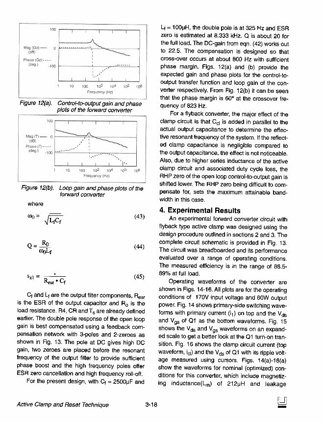
Figure 12(a). Control-to-output gain and phaseplots of the folWard converter
Figure 12(b). Loop gain and phase plots of thefo/Ward converter
where
roo = .,Ii:A" (43)
(44)Q=~
0>04
(45)LSzl = .--;-c;
~'esr
4 = 100IJH, the double pole is at 325 Hz and ESR
zero is estimated at 8.333 kHz. 0 is about 20 for
the full load. The DC-gain from eqn. (42) works out
to 22.5. The compensation is designed so that
cross-over occurs at about 800 Hz with sufficient
phase margin. Figs. 12(a) and (b) provide theexpected gain and phase plots for the control-to-
output transfer function and loop gain of the con-
verter respectively. From Fig. 12(b) it can be seen
that the phase margin is 60° at the crossover fre-
quency of 823 Hz.
For a flyback converter, the major effect of the
clamp circuit is that Ccl is added in parallel to theactual output capacitance to determine the effec-
tive resonant frequency of the system. If the reflect-
ed clamp capacitance is negligible compared to
the output capacitance, the effect is not noticeable.
Also, due to higher series inductance of the active
clamp circuit and associated duty cycle loss, the
RHP zero of the open loop control-to-output gain is
shifted lower. The RHP zero being difficult to com-
pensate for, sets the maximum attainable band-width in this case.
4. Experimental Results
An experimental forward converter circuit with
flyback type active clamp was designed using the
design procedure outlined in sections 2 and 3. Thecomplete circuit schematic is provided in Fig. 13.
The circuit was breadboarded and its performance
evaluated over a range of operating conditions.
The measured efficiency is in the range of 88.5-
89% at full load.
Operating waveforms of the converter areshown in Figs. 14-16. All plots are for the operating
conditions of 170V input voltage and 60W output
power. Fig. 14 shows primary-side switching wave-
forms with primary current (i1) on top and the Vds
and Vgs of 01 as the bottom waveforms. Fig. 15
shows the Vds and Vgs waveforms on an expand-
ed scale to get a better look at the 01 turn-on tran-
sition. Fig. 16 shows the clamp circuit current (top
waveform, icl) and the V ds of 01 with its ripple volt-
age measured using cursors. Figs. 14(a)-16(a)
show the waveforms for nominal (optimized) con-
ditions for this converter, which include magnetiz-
ing inductance(Lm) of 212IJH and leakage
Cf and 4 are the output filter components, Resr
is the ESR of the output capacitor and Ro is the
load resistance. R4, CR and T s are already defined
earlier. The double pole response of the open loop
gain is best compensated using a feedback com-
pensation network with 3-poles and 2-zeroes as
shown in Fig. 13. The pole at DC gives high DC
gain, two zeroes are placed before the resonant
frequency of the output filter to provide sufficient
phase boost and the high frequency poles offer
ESR zero cancellation and high frequency roll-off.
For the present design, with Cf = 2500~F and
[1!]-3-18Active Clamp and Reset Technique

x
.N26~ R"'1.5k
Cfp
1 330PF
R, C"
jl-I 10k .1"F
TL431
UCC3580.4
REF'~
T2~i. -1-i ~
RGI~I 30
IOUTI
j SHTDWN EAOUT
VDD EAIN
CLK SS
'OUT~ DELAY, R7'70k
R.200k
...5~140k
RAMP
LINE
I PGNC
OSC1
OSC2
GNDCT100D~-CR
.560pl-HOf,0k 5
*e
+
Figure 13. Detailed circuit schematic of the experimental forward converter
inductance(y) of about 2.5~H. The clamp capaci-
tance(Ccu is 9.4 nF. In Fig. 14(a), the current wave-
form indicates reflected load current of 1 A and
peak magnetizing current of 0.8A as designed. The
steady state Vds value is 274V with a D of 0.4
which matches the values derived from eqn. 1.
Figs. 14(b)-16(b) show the effect of adding an
external series inductance of 9~H (making total y= 11.5~H) which helps facilitate soft turn-on transi-
tion of 01. As can be seen from Fig. 14(b), the
actual duty cycle widens to 0.43 in this case for the
same operating conditions. This effect is attributed
to the loss of effective duty cycle introduced by the
additional inductance. The steady-state V ds is
impacted and it is higher by 20V in this case. The
impact on peak current levels is insignificant, but
the slopes of the current waveform during switch-
ing transition are observed to be less steep as a
result of higher series inductance. Figs. 14(c)-16(c)
are for the conditions where the magnetizing induc-
tance is reduced to 140IJH while maintaining the
9IJH series inductance. As shown in Fig. 14(c), the
peak of the magnetizing current goes up by about
50% to 1.5 A. Finally, Fig. 14(d)-16(d) are for the
conditions of lower magnetizing inductance and no
additional series inductance. Fig. 15(a) shows
that the resonant transition stops at about 100V
before the switch is turned on, thus indicating a
non-ZVS turn-on condition. With an added induc-
tance, Vds can go down to a lower value(60V)
0:::!]- 3-19 Active Clamp and Reset Technique

t
~(1A/d")
1~r K r
Vds(100y/div)
~ +"F
~
]
Figure 14(c). Lm = 140JlH, Lt= 11.5JlH
Figure 14. Primary side switching w~
even if starts from a higher value as shown in Fig.
15(b). The resonant transition allows true ZVS for
the circuit conditions depicted in Fig. 15(c).
However, the circuit efficiency in this case is actu-
ally lower due to the higher peak current and loss
of duty cycle contributed by the series inductance.
As shown in Fig. 15(d), the lower magnetizing
inductance contributes to a faster discharge (to
70V) of CA compared to Fig. 15(a) before the
switch turn-on. From Figs. 16(a) and (b), it is seen
that the V ds voltage ripple is 50V for the nominal
Lm and Ccl of 9.4 nF. By changing the Lm to a
smaller value, the ripple voltage goes up to BOV.
(Figs. 16(c) and (d)). Figs. 16(b) and (c) also show
the spike contributed to the clamp circuit current by
3-20Active Clamp and Reset Technique
Figure 14(d). Lm = 140.uH, y = 2.5.uH
veforms of the experimental converter
the additional inductance which also contributes to
the conduction losses. Finally, the impact of a
change in Ccl is illustrated in Fig. 16(e) where Ccl
is increased from 9.4 nF to 11.5 nF and the ripple
is reduced to 66V from 80V in Fig. 16(d).
An experimental flyback converter was also
designed and built using the design procedure out-
lined in this paper. Major changes from the forward
converter circuit included a flyback transformer
(same core size), modification to the output circuit
for flyback configuration, higher series inductance
(13.5 ~H), larger clamp switch (M1W8N60E) and
larger clamp capacitor (0.1 ~F). Other than the com-
pensation circuit, most of the other control circuitry
remains unchanged from the one shown in Fig. 13.

Figure 15(a). Lm = 212.uH, L, = 2.5.uH
Figure 15(c). Lm = 140JlH, y = 11.5JlH Figure 15(d). Lm = 140JlH, y = 2.5JlH
Figure 15. Expanded primary side waveforms (turn-on transition)
The converter efficiency was in the 83% range at step design procedure is included as a guide for
low line (8SV) and half load (SOW) condition. The designing active clamp forward and flyback convert-
efficiency is lower compared to the forward convert- ers. Many of the performance trade-offs faced when
er due to higher ripple current as discussed in sec- designing real life converters have been highlighted
tion 2. Some experimental waveforms of this circuit and quantified as appropriate, Practical results are
are shown in Fig. 17 for the same operating condi- given to illustrate the effects of certain design
tion. It can be seen from the bottom waveform that choices on the converter performance.
the main switch drain to switch voltage is extremely The advantages of the active clamp circuits
well-clamped (in the absence of any snubbers). The have been outlined and verified with a working lab
top waveform also shows the higher level of clamp prototype. The active clamp technique provides a
circuit current in this implementation, great avenue for enhancing the performance of the
Conclusions single-ended converters. These performanceP t ' I . I t d t th t ' I t h enhancements include switch voltage clamping,
rac Ica Issues re a e o e ac Ive c amp ec -
niques have been presented in this paper, A step by higher duty cycle operation, lossless switching and
reduced EMI, The additional circuit complexity
~- 3-21 Active Clamp and Reset Technique

Figure 16(b). Lm =212f.JH, y= 11.5f.JHFigure 16(8). Lm = 212J.iH, L, = 2.5J.iH
IA: BOVI,7l' '1
fr
T
'J..i-:!:~~/-r--~
IT
-"- r-oo
~
1"sldiv
Figure 16(d). Lm = 140/.lH, y = 2.5/.lH
Figure 16. Clamp circuit current andswitch voltage ripple
Figure 16(c). Lm = 140.uH, LI = 11.5.uH
" .'~(2A/dL) , I A: 66V
~.L+ \~~--~d..7 -/1
~. ., introduced by the active clamp circuit is easily off-
set by these advantages. In lower power convert-
ers, the complexity can be reduced by using the
boost type clamp circuit with p-channel switches.
In the past, the implementation of active clamp
converters involved using conventional PWM con-
trollers and additional logic and drive circuits.
However, such discrete implementations did not
fulfill some of the accuracy requirements specific to
the active clamp circuits such as maximum duty
cycle clamp, timing delays and unique protection
circuits. A new control IC which facilitates easy
implementation of the active clamp converters has
~~ Vds(100V/div)
W:+.~t+-=
ct
i~f.-
r
T .~div
Figure 16(e). Effects of Ccl increase(9.4nFto 11.5nF )
G=:!]-3-22Active Clamp and Reset Technique

[3] I.D. Jitaru, "Constant Frequency, Forward
Converter with Resonant Transition", HFPC
1991, pp. 282-292.
[4] J.A. Bassett, "Constant Frequency ZVS
Converter with Integrated Magnetics", APEC
1992, pp. 709-716.
[5] R. Watson, G.C. Hua and F.C. Lee,
"Characterization of an Active Clamp FlybackTopology for Power Factor Correction
Applications", APEC 1994, pp. 412-418.
[6] W. Andreycak, "Active Clamp and Reset
Technique Enhances Forward Converter
Performance", Unitrode Power Supply Design
Seminar SEM-1 000, 1994.
[7] D. Dalai and L. Wofford, "Novel Control IC for
Single-Ended Active Clamp Converters",
HFPC 1995, pp. 136-146.
[8] M. Schlecht, Tutorial material.
[9] G. Stojcic, F.C. Lee and S. Hiti, "Small-SignalCharacterization of Active-Clamp PWM
Converters", VPEC 1995, pp. 237-245.
DisclaimerPotential users of the IC product
described herein are advised that such use
could potentially violate patent rights of one or
more third parties. Unitrode disclaims any lia-
bility which may arise from applying this prod-
uct and suggests that users consult their own
legal advisors.
Figure 17. Clamp circuit current and mainswitch voltage for Active ClampFlyback Converter
been described. It is shown that the optimization of
active clamp forward and flyback converters is eas-ily achievable with the use of this new control IC -
UCC3580.
AcknowledgmentsThe author would like to acknowledge valuable
inputs and comments received during various
phases of this work from Lloyd Dixon, Bob
Mammano, Jim Noon, John O'Connor and Larry
Wofford. The author is also grateful to Chuck
Melchin for his willing help in the prototype building
and evaluation.
References[1] B. Carsten, "Epic Data Multi-Output Switched
Mode Power Supply", Epic Data internal
memo, Dec. 1978.
[2] B. Carsten, "Design Techniques for
Transformer Active Reset Circuits at High
Frequencies and Power Levels", HFPC 1990,
pp. 235-246.
G:=O- Active Clamp and Reset Technique3-23

IMPORTANT NOTICE
Texas Instruments and its subsidiaries (TI) reserve the right to make changes to their products or to discontinueany product or service without notice, and advise customers to obtain the latest version of relevant informationto verify, before placing orders, that information being relied on is current and complete. All products are soldsubject to the terms and conditions of sale supplied at the time of order acknowledgment, including thosepertaining to warranty, patent infringement, and limitation of liability.
TI warrants performance of its products to the specifications applicable at the time of sale in accordance withTI’s standard warranty. Testing and other quality control techniques are utilized to the extent TI deems necessaryto support this warranty. Specific testing of all parameters of each device is not necessarily performed, exceptthose mandated by government requirements.
Customers are responsible for their applications using TI components.
In order to minimize risks associated with the customer’s applications, adequate design and operatingsafeguards must be provided by the customer to minimize inherent or procedural hazards.
TI assumes no liability for applications assistance or customer product design. TI does not warrant or representthat any license, either express or implied, is granted under any patent right, copyright, mask work right, or otherintellectual property right of TI covering or relating to any combination, machine, or process in which suchproducts or services might be or are used. TI’s publication of information regarding any third party’s productsor services does not constitute TI’s approval, license, warranty or endorsement thereof.
Reproduction of information in TI data books or data sheets is permissible only if reproduction is withoutalteration and is accompanied by all associated warranties, conditions, limitations and notices. Representationor reproduction of this information with alteration voids all warranties provided for an associated TI product orservice, is an unfair and deceptive business practice, and TI is not responsible nor liable for any such use.
Resale of TI’s products or services with statements different from or beyond the parameters stated by TI forthat product or service voids all express and any implied warranties for the associated TI product or service,is an unfair and deceptive business practice, and TI is not responsible nor liable for any such use.
Also see: Standard Terms and Conditions of Sale for Semiconductor Products. www.ti.com/sc/docs/stdterms.htm
Mailing Address:
Texas InstrumentsPost Office Box 655303Dallas, Texas 75265
Copyright 2001, Texas Instruments Incorporated