design considerations for cmos-integrated hall-effect...
TRANSCRIPT
Design Considerations for CMOS-Integrated Hall-effect Magnetic Bead
Detectors for Biosensor Applications
by
Karl Ryszard Skucha
A dissertation submitted in partial satisfaction of the
requirements for the degree of
Doctor of Philosophy
in
Engineering – Electrical Engineering and Computer Sciences
in the
Graduate Division
of the
University of California, Berkeley
Committee in charge:
Professor Bernhard E. Boser, Chair
Professor Ming Wu
Professor Luke Lee
Fall 2012
Design Considerations for CMOS-Integrated Hall-effect Magnetic Bead
Detectors for Biosensor Applications
Copyright © 2012
by
Karl Ryszard Skucha
1
Abstract
Design Considerations for CMOS-Integrated Hall-effect Magnetic Bead Detectors
for Biosensor Applications
by
Karl Ryszard Skucha
Doctor of Philosophy in
Electrical Engineering and Computer Sciences
University of California, Berkeley
Professor Bernhard E. Boser, Chair
This dissertation presents a design methodology for on-chip magnetic bead
label detectors based on Hall-effect sensors to be used for biosensor applications.
Signal errors caused by the label-binding process and other factors that place con-
straints on the minimum detector area are quantified and adjusted to meet assay ac-
curacy standards. The methodology is demonstrated by designing an 8,192 element
Hall sensor array implemented in a commercial 0.18 µm CMOS process with single
mask post-processing. The array can quantify a one percent surface coverage of 2.8
µm beads in thirty seconds with a coefficient of variation of 7.4%. This combination
of accuracy and speed makes this technology a suitable detection platform for bio-
logical assays based on magnetic bead labels.

i
To my grandmother Stefania.
ii
Table of contents
1 Introduction ..................................................................................................1
1.1 Immuno-Chromatographic strip tests ................................................1
1.2 Enzyme-linked immunosorbent assay (ELISA) ................................2
1.3 Magnetic label immunoassay (MIA) .................................................3
2 System performance and error analysis .......................................................6
2.1 Overview ............................................................................................6
2.2 Error sources ......................................................................................7
2.3 Minimum detection area ..................................................................10
2.4 Summary ..........................................................................................12
3 Magnetic labels and magnetic detectors ....................................................13
3.1 Magnetic labels ................................................................................13
3.2 Magnetic label detectors ..................................................................16
3.3 Detection methods ...........................................................................17
3.4 Summary ..........................................................................................19
4 Hall-effect bead detector design ................................................................20
4.1 Hall effect .........................................................................................20
4.2 Bead detector architecture ................................................................21
4.3 Post processing.................................................................................24
4.4 Polarization field generator architecture ..........................................26
4.5 Sensor non-idealities and measurement algorithm ..........................30
4.6 Test array implementation and results .............................................33
4.7 Summary ..........................................................................................42
5 Bead detector array ....................................................................................44
5.1 Array design and optimization .........................................................44
5.2 Bias and readout circuits ..................................................................49
5.3 Measurement results ........................................................................56
5.3.1 Sensor characterization ............................................................56
5.3.2 Array characterization ..............................................................57
5.3.3 Signal demodulation using thresholding ..................................61
5.4 Assay results ....................................................................................63
6 Conclusion .................................................................................................65
7 References ..................................................................................................66
iii
List of figures
Figure 1-1: Immuno-chromatographic test operation. ...................................................2
Figure 1-2: ELISA protocol. ..........................................................................................3
Figure 1-3: Magnetic immunoassay (MIA) protocol .....................................................4
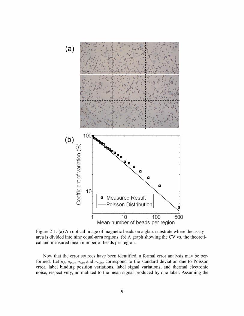
Figure 2-1: (a) An optical image of magnetic beads on a glass substrate where the assay
area is divided into nine equal-area regions. (b) A graph showing the CV vs. the
theoretical and measured mean number of beads per region. ................................9
Figure 2-2: Minimum detection area for an assay with a DRlabel of 100 utilizing 2.8 µm
labels vs. the desired CV. .....................................................................................11
Figure 3-1: Composition of a microbead and response to an external field. ...............14
Figure 3-2: Magnetization curve at room temperature for M-280 (left) and M-450 (right)
[29]. ......................................................................................................................15
Figure 3-3: Conventional label detection method based on magnetization/polarization.17
Figure 3-4: Relaxation detection method. ....................................................................18
Figure 4-1: The principle of Hall Effect. .....................................................................21
Figure 4-2: Cross-section of a Hall-effect bead detector showing relevant magnetic fields.
..............................................................................................................................22
Figure 4-3: (a) Schematic showing magnetic field lines from a magnetized bead passing
through a loop of radius r, (b) total magnetic flux passing through the loop vs. radius
r of the loop, and (c) average magnetic field passing through the loop vs. radius r.
..............................................................................................................................23
Figure 4-4: Magnetic field strength of a bead placed directly over a Hall sensor vs. the
distance of the bead surface from the Hall sensor................................................24
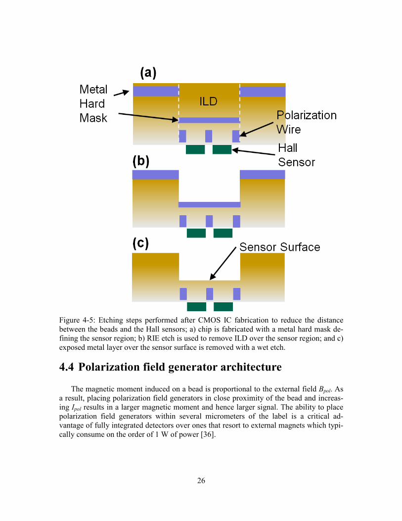
Figure 4-5: Etching steps performed after CMOS IC fabrication to reduce the distance
between the beads and the Hall sensors; a) chip is fabricated with a metal hard mask
defining the sensor region; b) RIE etch is used to remove ILD over the sensor
region; and c) exposed metal layer over the sensor surface is removed with a wet
etch. ......................................................................................................................26
Figure 4-6: Polarization field generators based on: a) polarization wires and b)
polarization coils. .................................................................................................27
Figure 4-7: Ratio of the average Hall voltage signal of the polarization wire architecture
to the polarization coil architecture as a function of the ratio of z/a, where z is the
vertical distance from the bead center to the plane of the polarization coils/wires and
a is the radius of the coils or half the distance between polarization wires. ........29
Figure 4-8: Thermal simulations of the bead detector: (a) cross section across a single
row of sensors showing temperature gradients from the polarization lines to the
silicon substrate, (b) top view of a 200 µm current line showing thermal gradients in
the silicon substrate below the line. .....................................................................31
Figure 4-9: Measurement algorithm for detecting magnetic beads. ............................32
Figure 4-10: Example of a signal before CDS (blue) including both offset and thermal
effects and after CDS (red), where DC offset and thermal effects are cancelled.33
iv
Figure 4-11: Unit-cells of both the n-well and MOS Hall sensor array implementations.
..............................................................................................................................34
Figure 4-12: (a) Normalized signal as a function of the position of one magnetic bead
over the n-well sensor (left) and MOS sensor (right) on horizontal line H-H’, shown
in Figure 4-11. (b) Normalized signal as a function of the position of one magnetic
bead over the n-well sensor (left) and MOS sensor (right) on vertical line V-V’,
shown in Figure 4-11. The total signal is the sum of the signals of the center sensor
and adjacent sensors. The points and error bars show measured results. ............36
Figure 4-13: Total voltage signal from all sensors in the array for three different bead
types vs. (a) number of beads on the array, (b) percent of array area the beads cover,
and (c) total volume of iron oxides (ferrites) from the beads on the surface of the
array. .....................................................................................................................38
Figure 4-14: Optical vs. magnetic images of magnetic beads on n-well and MOS Hall
sensor arrays.........................................................................................................39
Figure 4-15: (a) Pre-CDS response of Hall sensors at different regions in the 8x8 array.
The gray squares represent dummy sensors and the white squares represent active
sensors, (b) graph showing maximum error due to thermal effects for 6 mA and 25
mA Ipol vs. excitation frequency of the polarization line. .....................................41
Figure 4-16: Measurements of signal amplitude from one row of sensors over a time span
of 90 minutes........................................................................................................42
Figure 5-1: Array architecture. .....................................................................................45
Figure 5-2: Contour plots of FOM and maximum surface temperature rise for various
values of polarization current and number of sensors per row. ...........................47
Figure 5-3: (a) Optical image of the sensor chip containing 4 banks with 2048 active
sensors each. (b) One half of a 2048 Hall sensor array bank with M280 beads
covering approximately 2% of the surface. .........................................................49
Figure 5-4: Array and electronics block diagram. .......................................................50
Figure 5-5: Readout channel schematic. ......................................................................51
Figure 5-6: V-I converter operation, from top to bottom Φ1 (Auto-zero), Φ2 (First
integration), Φ3 (idle) and Φ4 (second integration) ..............................................52
Figure 5-7: Gm-stage schematic with annotated transistor sizes ..................................53
Figure 5-8: Circuit Schematics of A/D Converter building blocks: D/A (left) and OTA
(right) ...................................................................................................................55
Figure 5-9: Sum of all bead signals from all sensors vs. number of beads placed on the
array .....................................................................................................................58
Figure 5-10: Coefficient of variation vs. number of beads placed on the array for various
error sources. Points indicate measured results and lines indicate simulated or
calculated values ..................................................................................................59
Figure 5-11: Required detection time to achieve a CVlabel of 7.4% and DRlabel of 100 vs.
bead diameter for sensor based on the 32 mA and 128 mA polarization currents.61
Figure 5-12: Measurement time per sensor required to quantify 13 beads with a CVnoise of
15% vs. number of sensors in the array ...............................................................63
v
Figure 5-13: HSA assay using 2.8µm labels: normalized signal output vs. HSA
concentration. Optical photos of the measured sensor array are also shown for each
measured concentration. ......................................................................................64
vi
Acknowledgements
I would like to first thank my family, namely my grandmother Stefania, my parents
BoŜena and Ryszard, and my sister Ewa and brother Tomasz, who have been instrumental
in my development and education from the day I was born through the last days of my
graduate studies. This work was made possible by their many sacrifices and continuous
support of my efforts. I also want to thank my brother-in-law Bartek and sister-in-law
Sylwia for their encouragement and my wonderful nieces Klaudia, Kaya, Zosia and my
nephew Anthony for bringing joy to my life during my tenure at Cal.
My work was built upon the efforts and results of many others who have come before
me, including Turgut Aytur, Mekhail Anwar, Prof. Eva Harris, Prof. Robert Beatty, and
my advisor, Prof. Bernhard Boser, who had the vision to embark on this long-term re-
search project. Special thanks also go to Octavian Florescu, who masterminded critical
improvements and additional features that turned this project into a real product, further
guiding and motivating my efforts.
My greatest thanks go to the ones whom I worked with on a day-to-day basis. Fore-
most, I thank Paul Liu, who was my partner in crime in designing the bead detector sys-
tem and developing the relaxation detection method. I thank Mischa Megens for his ex-
pert advice on all things “physics” and for crafting the backbone of the MATLAB simula-
tor often used in this work. I thank Simone Gambini for providing his expert chip design
and circuits knowledge and for designing and testing the readout circuitry for the bead
detector array presented in chapter 5. I thank Jungkyu Kim for providing his expertise in
performing bioassays. I give thanks to Yida Duan, Igor Izyumin, Richard Przybyla, and
Mitchell Kline for all their help, the interesting discussions we’ve had, and for all the fun
times we had spent together. Finally, I thank my advisor, Prof. Bernhard Boser, for unre-
lentingly setting high standards on all my work and pushing my abilities to the limit.
I would like to express my gratitude to the BSAC staff, especially John Huggins,
Richard Lossing, Alain Kesseru, and Helen Kim, who worked tirelessly to organize all
the BSAC events and raise funding for BSAC researchers, myself among them. I thank
the Microlab staff, including Bill Flounders, Sia Parsa, Joe Donnelly, Kim Chan, Marilyn
Kushner, and the late Jimmy Chang, for their advice, training, and for providing me with
the resources needed to complete my work. I want to also thank the EECS staff, including
Patrick Hernan, Ruth Gjerde, and Shirley Salanio for providing the needed support in
teaching and research matters.
Finally, I cannot express enough gratitude to my girlfriend, Haleh Razavi, without
whom I would not be writing these words in the first place. She has incessantly encour-
aged me not to give up, even though I wanted to do so many times. Her presence in my
life not only made this journey tolerable, but truly joyful, and I hope we can share that
joy well beyond graduation day. Kheily mamnoon, Azize-Delam.
1
1 Introduction
Biochemical assays are used in medical diagnostic testing for many conditions in-
cluding infectious diseases, heart attack, and cancer [1]. There is a growing need for
technological solutions that enable diagnostic testing in diverse point-of-care (POC) set-
tings, including local clinics in the developing world and physician offices and patients’
homes in the developed world [2]. Specifications involving sensitivity, specificity, porta-
bility, affordability, and accuracy need to be met for each POC application without de-
pending on existing laboratory infrastructure.
1.1 Immuno-Chromatographic strip tests
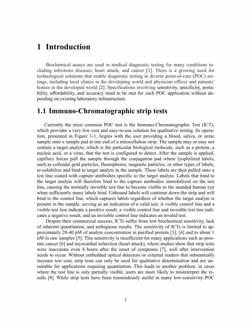
Currently the most common POC test is the Immuno-Chromatographic Test (ICT),
which provides a very low cost and easy-to-use solution for qualitative testing. Its opera-
tion, presented in Figure 1-1, begins with the user providing a blood, saliva, or urine
sample onto a sample pad at one end of a nitrocellulose strip. The sample may or may not
contain a target analyte, which is the particular biological molecule, such as a protein, a
nucleic acid, or a virus, that the test is configured to detect. After the sample is applied,
capillary forces pull the sample through the conjugation pad where lyophilized labels,
such as colloidal gold particles, fluorophores, magnetic particles, or other types of labels,
re-solubilize and bind to target analyte in the sample. These labels are then pulled onto a
test line coated with capture antibodies specific to the target analyte. Labels that bind to
the target analyte will therefore bind to the capture antibodies immobilized on the test
line, causing the normally invisible test line to become visible to the unaided human eye
when sufficiently many labels bind. Unbound labels will continue down the strip and will
bind to the control line, which captures labels regardless of whether the target analyte is
present in the sample, serving as an indication of a valid test. A visible control line and a
visible test line indicate a positive result, a visible control line and invisible test line indi-
cates a negative result, and an invisible control line indicates an invalid test.
Despite their commercial success, ICTs suffer from low biochemical sensitivity, lack
of inherent quantitation, and ambiguous results. The sensitivity of ICTs is limited to ap-
proximately 20-40 pM of analyte concentration in purified protein [3], [4] and to about 1
nM in raw samples [5]. This sensitivity is insufficient for many applications such as pros-
tate cancer [6] and myocardial infarction (heart attack), where studies show that strip tests
were inaccurate even 4 hours after the onset of symptoms [7], well after intervention
needs to occur. Without embedded optical detectors or external readers that substantially
increase test cost, strip tests can only be used for qualitative determination and are un-
suitable for applications requiring quantitation. This leads to another problem: in cases
where the test line is only partially visible, users are more likely to misinterpret the re-
sults [8]. While strip tests have been tremendously useful in many low-sensitivity POC
2
applications, they are unsuitable for a range of biomarker applications where more sensi-
tive and/or quantitative detection are needed.
Figure 1-1: Immuno-chromatographic test operation.
1.2 Enzyme-linked immunosorbent assay (ELISA)
Many laboratory immunoassays used today based are based on colorimetric or fluo-
rescent detection methods and provide sufficient sensitivity for the aforementioned appli-
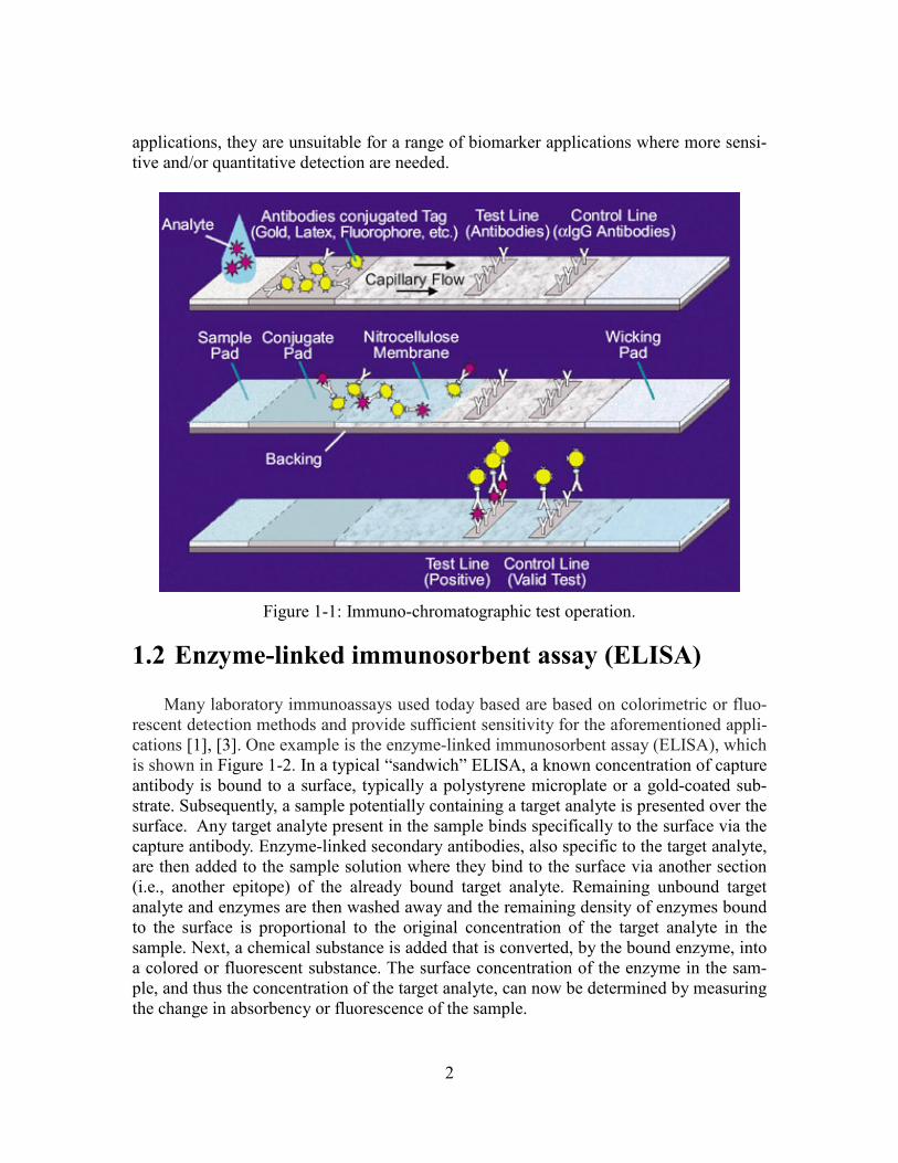
cations [1], [3]. One example is the enzyme-linked immunosorbent assay (ELISA), which
is shown in Figure 1-2. In a typical “sandwich” ELISA, a known concentration of capture
antibody is bound to a surface, typically a polystyrene microplate or a gold-coated sub-
strate. Subsequently, a sample potentially containing a target analyte is presented over the
surface. Any target analyte present in the sample binds specifically to the surface via the
capture antibody. Enzyme-linked secondary antibodies, also specific to the target analyte,
are then added to the sample solution where they bind to the surface via another section
(i.e., another epitope) of the already bound target analyte. Remaining unbound target
analyte and enzymes are then washed away and the remaining density of enzymes bound
to the surface is proportional to the original concentration of the target analyte in the
sample. Next, a chemical substance is added that is converted, by the bound enzyme, into
a colored or fluorescent substance. The surface concentration of the enzyme in the sam-
ple, and thus the concentration of the target analyte, can now be determined by measuring
the change in absorbency or fluorescence of the sample.
3
ELISAs are generally regarded as the gold standard for immunoassays performed in
laboratory settings [1], [2]. However, these assays are difficult to use in POC settings for
two reasons. First, ELISAs require lengthy incubation times, particularly because it takes
a long time for the target analyte to diffuse to the surface where it can bind to the capture
antibody and also because enzymatic reactions typically take over an hour to produce de-
tectable signals [1]. Second, optical detectors that are capable of detecting slight color
changes are expensive to manufacture and thus are not compatible with disposable POC
devices [2]. In particular, it is very difficult to measure color changes using complemen-
tary metal-oxide-semiconductor (CMOS) technologies without applying specific filters to
filter out ambient light and, in the case of fluorescent detection, filters to block light used
to excite fluorescent particles [2].
Figure 1-2: ELISA protocol.
1.3 Magnetic label immunoassay (MIA)
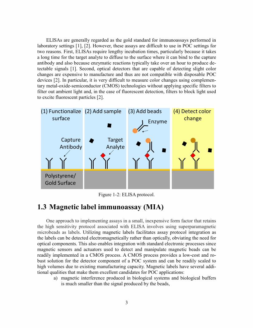
One approach to implementing assays in a small, inexpensive form factor that retains
the high sensitivity protocol associated with ELISA involves using superparamagnetic
microbeads as labels. Utilizing magnetic labels facilitates assay protocol integration as
the labels can be detected electromagnetically rather than optically, obviating the need for
optical components. This also enables integration with standard electronic processes since
magnetic sensors and actuators used to detect and manipulate magnetic beads can be
readily implemented in a CMOS process. A CMOS process provides a low-cost and ro-
bust solution for the detector component of a POC system and can be readily scaled to
high volumes due to existing manufacturing capacity. Magnetic labels have several addi-
tional qualities that make them excellent candidates for POC applications:
a) magnetic interference produced in biological systems and biological buffers
is much smaller than the signal produced by the beads,
(2) Add sample
Enzyme
(3) Add beads(1) Functionalize
surface
Target
Analyte
Capture
Antibody
Polystyrene/
Gold Surface
(4) Detect color
change
4
b) magnetic beads are stable in biological solutions and in lyophilized form, en-
abling robust detection and long shelf life,
c) magnetic beads are amenable to remote manipulation via electromagnetic
means, which can enable integrated mixing and washing steps for a fast and
highly integrated assay protocol [9], [10],
d) single individual magnetic beads can be detected with high signal-to-noise ra-
tio (SNR), enabling robust and rapid bead detection methods, and
e) magnetic beads can be detected in opaque buffers.
Figure 1-3 shows an example of a sandwich immunoassay utilizing magnetic beads
as labels that is performed on a microchip with integrated magnetic detectors. First, the
surface of the chip is functionalized with capture antibodies that specifically bind to a
target analyte being detected. In the second step, an aqueous sample containing the target
analyte is introduced and the target analyte binds to the surface via the capture antibodies.
Subsequently or concurrently, magnetic bead labels are introduced and bind to the target
analyte via conjugated detection antibodies specific to another epitope of the target
analyte. Any non-specifically bound beads may be removed using magnetic forces [9],
[11] or hydrodynamic forces if the chip is integrated into a microfluidic system [12]. The
remaining specifically bound beads can then be detected and used to infer the initial con-
centration of target analyte.
Figure 1-3: Magnetic immunoassay (MIA) protocol
On the surface the protocol associated with ELISA and MIA appears very similar.
Aside from the obvious difference in type of label, one difference is the size of the label.
Label size affects label diffusion behavior, binding behavior, and signal strength; chang-
ing the size of the label often requires changes in the entire assay protocol and is difficult
to analyze beyond experimental means. Small labels used in ELISAs and other laboratory
tests, such as fluorophores or enzymes, have dimensions that are similar to target analytes
(2) Add sample
Magnetic
Bead
(3) Add beads(1) Functionalize
surface
Target
Analyte
Capture
Antibody
Magnetic
Sensor
Magnetic
Sensor
Magnetic
Sensor
Magnetic
Sensor
(4) Detect beads
5
such as antibodies, which are on the order of 5 nm. Labels much larger than the target
analytes are much less typical. As will be explained in chapter 2, large labels require larg-
er detector areas but have the advantage of being easily manipulated via electromagnetic
or hydrodynamic forces to enable mixing and to increase surface contact, resulting in a
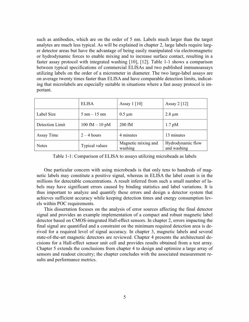
faster assay protocol with integrated washing [10], [12]. Table 1-1 shows a comparison
between typical specifications of commercial ELISAs and two published immunoassays
utilizing labels on the order of a micrometer in diameter. The two large-label assays are
on average twenty times faster than ELISA and have comparable detection limits, indicat-
ing that microlabels are especially suitable in situations where a fast assay protocol is im-
portant.
ELISA Assay 1 [10] Assay 2 [12]
Label Size 5 nm – 15 nm 0.5 µm 2.8 µm
Detection Limit 100 fM – 10 pM 200 fM 1.7 pM
Assay Time 2 – 4 hours 4 minutes 13 minutes
Notes Typical values Magnetic mixing and
washing
Hydrodynamic flow
and washing
Table 1-1: Comparison of ELISA to assays utilizing microbeads as labels
One particular concern with using microbeads is that only tens to hundreds of mag-
netic labels may constitute a positive signal, whereas in ELISA the label count is in the
millions for detectable concentrations. A result inferred from such a small number of la-
bels may have significant errors caused by binding statistics and label variations. It is
thus important to analyze and quantify these errors and design a detector system that
achieves sufficient accuracy while keeping detection times and energy consumption lev-
els within POC requirements.
This dissertation focuses on the analysis of error sources affecting the final detector
signal and provides an example implementation of a compact and robust magnetic label
detector based on CMOS-integrated Hall-effect sensors. In chapter 2, errors impacting the
final signal are quantified and a constraint on the minimum required detection area is de-
rived for a required level of signal accuracy. In chapter 3, magnetic labels and several
state-of-the-art magnetic detectors are reviewed. Chapter 4 presents the architectural de-
cisions for a Hall-effect sensor unit cell and provides results obtained from a test array.
Chapter 5 extends the conclusions from chapter 4 to design and optimize a large array of
sensors and readout circuitry; the chapter concludes with the associated measurement re-
sults and performance metrics.
6
2 System performance and error analysis
2.1 Overview
The primary goal of a point-of-care diagnostic assay is to provide an accurate reading
of the concentration of the target analyte under certain constraints. While these con-
straints vary among different applications, in general, the detection component of a point-
of-care tester needs to:
a) be inexpensive as the total system cost is limited to a few dollars [13],
b) be powered by a battery that is AAA or smaller to enable portability, and
c) perform the detection step in less than one minute as the entire assay, includ-
ing any necessary incubation steps, needs to complete in 5-10 minutes.
From these requirements we see that detection area, energy consumption, and readout
time are relevant performance metrics that should be considered and minimized during
the design process while maintaining a certain level of readout accuracy as determined by
the application.
When an assay is performed many times under the same conditions (i.e., same analyte
concentration, same temperature etc.), the results vary with a Gaussian distribution where
the mean of the results is µ and the standard deviation of the results is σ. To quantify as-
say accuracy, commercial assay kits commonly provide the user with a standard curve
describing the relationship between the output signal and the analyte concentration and a
coefficient of variation (CV) defined as:
�� ��� (1)
The CV determines the relative accuracy of an assay, while the standard curve allows one
to map the output signal from the detector to the actual analyte concentration.
Assays for different applications have varying accuracy and dynamic range require-
ments. The dynamic range of an assay is defined as the ratio of the highest detectable
concentration to the lowest detectable concentration. In some cases, as in a C-reactive
protein (CRP) assays, high dynamic range is required as CRP levels vary by as much as
five orders of magnitude [14]. In other cases, such as in hemoglobin A1c assays, high ac-
curacy is required as differences of several percent result in different treatment plans
[15]. In general, it is desirable to have a CV of 2% – 20% over several orders of magni-
tude of analyte concentration [16]. While both the standard curve and the CV are largely
dependent on and often limited by the biological reagents used, it is important to ensure
that the characteristics of the labels and the detection system do not unnecessarily de-
grade assay accuracy.
Before discussing error sources contributing to the CV, we need to relate the label
signal, defined as the total signal from all labels situated on the sensors, to the analyte
concentration being measured. In many assays this relationship is non-linear and, in the
region between the limit of detection and saturation, can be described by a power law
7
given by:
�� ∝ �� (2)
where [A] is the analyte concentration, n is the number of labels on the surface, and the
exponent x is typically between 1-3 for published magnetic bead assays [12], [17], [18].
This non-linearity stems from the non-uniformity of binding affinities between individual
analyte-antibody pairs and steric effects associated with the analyte and labels [19]. For
small CVs, the non-linearity results in the relationship between CVlabel and CV[A] of:
��� � � ∙ ������� (3)
The non-linearity in the standard curve effectively reduces the accuracy. For example, for
a square law relation between labels and analyte concentration (i.e., x = 2), a CVlabel of
10% results in a CV[A] of 20%.
2.2 Error sources
Several error sources are present in label detectors that can significantly impact the
CV of the label signal. Some, like electronic noise, are present in all detector systems,
whereas errors due to label variations, label binding location variations, and the label
binding process are of particular concern in cases where a small number of labels consti-
tute the final signal. Electronic noise comes from thermal noise and flicker noise generat-
ed by sensors and detection electronics. It is desirable to keep the flicker noise corner fre-
quency below the measurement bandwidth and to average or integrate the signal to re-
duce thermal noise to the required level. Label variations arise from variations in label
size and/or variations in the signal each label generates (e.g., variations in magnetic con-
tent for magnetic labels) and have a standard deviation between 10%−30% for magnetic
beads used in this work. Label binding position variations come from location-dependent
sensitivity of the detectors and depend on the sensor design, which is discussed in more
detail in chapters 4 and 5.
In general, with a proper detector design, sufficient readout time, and suitable labels,
the aforementioned error sources can be kept small. However, signal variations from the
label binding process pose a fundamental error source in immunoassays. The binding of a
capture antibody to its target analyte is a probabilistic event and follows dynamics that
are common to all affinity-based biosensors and are known to generate biological shot
noise [20]. Since each capture event is unlikely (esp. at low target analyte concentrations)
and approximately independent of the others and since many such events occur, the num-
ber of labels bound to the sensor surface can be described by a Poisson distribution,
where the standard deviation of the number of labels is equal to the square root of the
mean number of labels. This error source is negligible in assays using large amounts of
small labels such as enzymes or fluorophores, but in the case that only tens to hundreds
of labels make up the final label signal, this error is significant and is further analyzed
below.
Given that the number of labels bound to the surface for a particular analyte concen-
8
tration has mean n, then according to the Poisson distribution the standard deviation is √�
and the CV (CVP) is CVP = √� � � 1 √�⁄⁄ . Thus, the minimum number of labels re-
quired to achieve a certain CVP is given by:
� � 1���� (4)
For example, 400 labels are required to achieve a CVP of 5%. This variation can be re-
duced only by increasing the number of bound labels, which, for a given analyte concen-
tration, requires an increase of the sample volume and detection area.
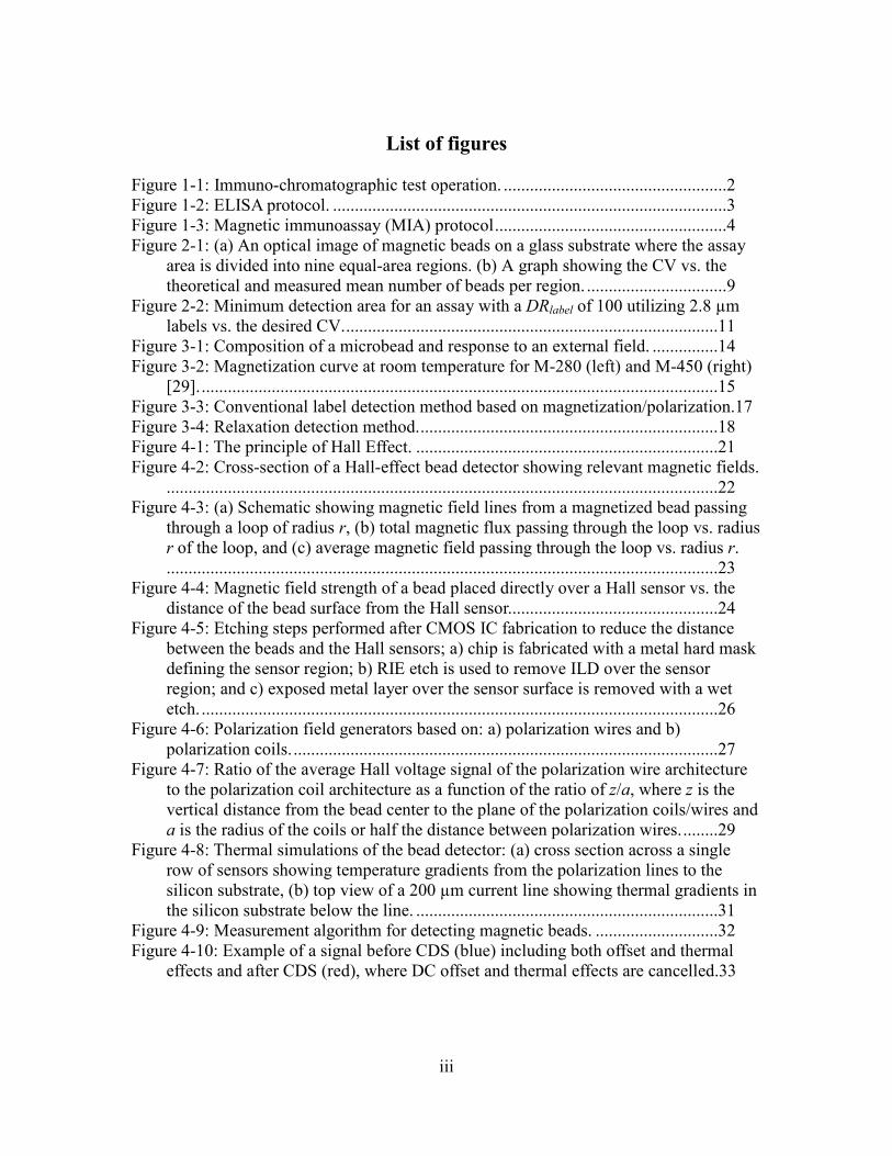
Figure 2-1 (a) and (b) confirm the above analysis of Poisson error for magnetic bead
label binding. A magnetic bead immunoassay was performed on a glass substrate using
100 ng/mL of mouse IgG as the target analyte. The total assay area was divided into mul-
tiple, equal-area regions (Figure 2-1 (a)) and the mean, standard deviation, and CV of the
number of beads in the regions were calculated. The calculations were then repeated for
smaller regions and the CV was plotted vs. mean number of beads per region in Figure
2-1 (b). A close correlation between the measured data and the theoretical Poisson distri-
bution given by Eq. (4) is observed. This analysis effectively treats each region as a sepa-
rate assay and rejects other variations, such as inconsistencies in sample preparation and
delivery steps, variations in amounts of biological reagents used, and environmental ef-
fects, which would normally occur between different assays and further increase the CV.
Thus the Poisson error sets the lower limit for the CV, and the final CV may be higher
due to the aforementioned effects external to the detector system.
9
Figure 2-1: (a) An optical image of magnetic beads on a glass substrate where the assay
area is divided into nine equal-area regions. (b) A graph showing the CV vs. the theoreti-
cal and measured mean number of beads per region.
Now that the error sources have been identified, a formal error analysis may be per-
formed. Let σP, σpos, σsig, and σnoise correspond to the standard deviation due to Poisson
error, label binding position variations, label signal variations, and thermal electronic
noise, respectively, normalized to the mean signal produced by one label. Assuming the
(a)
(b)
10
aforementioned error sources are independent and noting that σP = 1, the total CV (i.e.,
CVlabel) is given by:
������� � ������� � �� � ������ � ������ � �!������
(5)
where n is the number of labels and N is the total number of sensors forming the detec-
tion area. Just like the Poisson error, the errors from label position variations and label
signal variations scale with √�, whereas errors due to electronic noise depend on the total
number of sensors and thus are constant for a particular number of sensors and a particu-
lar measurement time per sensor. Assuming electronic noise can be made small by aver-
aging the sensor signals over a sufficiently long measurement time, the minimum number
of labels required to attain a certain CVlabel and CV[A] is given by:
� � 1 � ����� � ������������� � ��"1 � ����� � ����� #��� � (6)
Recall that x is the exponent in the power law relationship between the number of la-
bels and the analyte concentration, and as expected, Eq. (6) reduces to Eq. (4) when error
sources from label position variations and label variations are negligible. For example,
for x = 2 and assuming σpos = 0.3 and σsig = 0.3, which are the approximate values for the
sensor array and labels presented in chapter 4, for a CV[A] of 10%, the minimum number
of bound labels is n = 435.
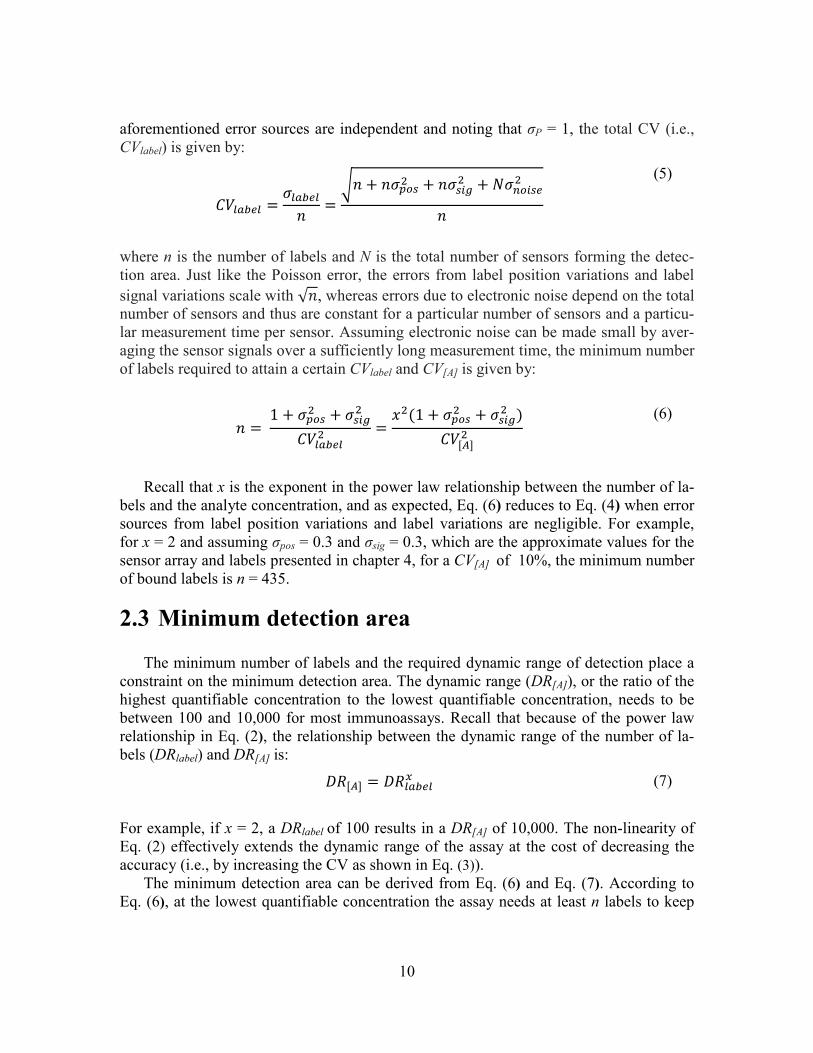
2.3 Minimum detection area
The minimum number of labels and the required dynamic range of detection place a
constraint on the minimum detection area. The dynamic range (DR[A]), or the ratio of the
highest quantifiable concentration to the lowest quantifiable concentration, needs to be
between 100 and 10,000 for most immunoassays. Recall that because of the power law
relationship in Eq. (2), the relationship between the dynamic range of the number of la-
bels (DRlabel) and DR[A] is:
$%� � $%������ (7)
For example, if x = 2, a DRlabel of 100 results in a DR[A] of 10,000. The non-linearity of
Eq. (2) effectively extends the dynamic range of the assay at the cost of decreasing the
accuracy (i.e., by increasing the CV as shown in Eq. (3)).
The minimum detection area can be derived from Eq. (6) and Eq. (7). According to
Eq. (6), at the lowest quantifiable concentration the assay needs at least n labels to keep
11
Poisson error within a required CV[A], whereas, according to Eq. (7), at the highest
analyte concentration at least n × DRlabel labels need to bind to the surface. Assuming that
at saturation the surface is approximately fully covered with labels, the required detection
area is:
� & '� ∙ $%����� ∙ � � '� ∙ $%� ( �⁄ ��"1 � ����� � ����� #��� �
(8)
where d is the label diameter. Figure 2-2 shows the relationship between the minimum
detection area and CV[A] for 2.8 µm diameter labels with x = 2, DR[A] of 10,000, σpos =
0.3, and σsig = 0.3.
Figure 2-2: Minimum detection area for an assay with a DRlabel of 100 utilizing 2.8 µm
labels vs. the desired CV.
Several interesting implications can be derived from Eq. (8) and Figure 2-2. First, the
non-linearity in the standard curve actually helps to reduce the required detection area as
the term $%� ( �⁄ �� decreases as x becomes larger for typical values of DR[A]. Second, the
detection areas for a high accuracy assays (CV[A] < 5%) utilizing 2.8 µm labels are on the
order of 1 mm2 and are readily attainable on CMOS chips. Labels larger than 10 µm,
however, are not suitable for on-chip assays as they would require areas in excess of 10
mm2 just for the sensors, a size that would be impractical due to high chip costs.
0.01
0.1
1
10
100
0 5 10 15 20 25 30
Min
. D
ete
ctio
n A
rea
(m
m2)
CV[A] (%)
12
The above analysis derives the minimum required detection area as a function of label
size and assay accuracy and is not limited to solely magnetic sensors and magnetic labels;
it can be applied to any type of sensor or sensor array designed to detect labels, for exam-
ple, fluorescent or colored beads in conjunction with optical detectors [21–23]. Since it is
desirable to keep the detection area as small as possible, the errors from non-Poisson er-
ror sources should be made smaller or equal to the Poisson error during the design and
detection processes. Additionally, the detection time and energy should also be mini-
mized, which, for many sensor types, is most effectively achieved by maximizing the
signal detected by each sensor. The next chapter will introduce the properties of magnetic
bead labels and discuss state-of-the-art sensor technologies used for their detection.
Chapter 4 will apply the analysis provided here and the properties of magnetic particles
discussed in the next chapter to the design and optimization of Hall-effect sensors for the
detection of magnetic bead labels.
2.4 Summary
Immunoassays are characterized by a standard curve that maps the output signal to
the analyte concentration and a coefficient of variance (CV) that describes the normalized
variations in the assay. A detector needs to be designed with a CV in a clinically relevant
range (e.g., between 2% − 20%) over a clinically relevant dynamic range of analyte con-
centration (e.g., 100 – 10,000). Errors stemming from the detector, errors fundamental to
the label binding process, and the finite size of the label set constraints on the minimum
detection area, which is on the order of 1 mm2 for high accuracy immunoassays utilizing
micron-sized labels and can readily be implemented on CMOS chips.

13
3 Magnetic labels and magnetic detectors
Magnetic bead labels are abundant at biological laboratories and pharmaceutical
companies as they are very useful in separating one molecule or cell from another in a
solution, a process that is commonly performed. Due to their high prevalence, favorable
properties presented in chapter 1, and enablement of highly integrated sensing systems
utilizing magnetic sensors, they make excellent candidates for assay labels. In this chap-
ter, we discuss the properties of magnetic assay labels and review various technologies
used for their detection in bioassay applications.
3.1 Magnetic labels
Magnetic microbeads and nanoparticles have been widely used in biomedical applica-
tions, such as cell separation and medical imaging [24], and recently they have been uti-
lized as labels in diagnostic tests [12], [17], [18], [25–27]. The magnetic beads used for
this work are the popular and commercially available Dynabeads® (Invitrogen Inc, Oslo,
Norway). These beads are made up of iron-oxide nano-particles enclosed in a spherical
polymer matrix, as shown in Figure 3-1. The iron-oxide particles are on the order of 10
nm to 20 nm in diameter and the beads used in this thesis are between 1 µm to 4.5 µm in
diameter [28]. In the absence of an external magnetic field, each magnetic nanoparticle
forms a magnetic dipole with a magnetic moment pointing in a random direction. Conse-
quently, the individual magnetic fields from each nanoparticle cancel out and the bead as
a whole does not generate a measurable magnetic field.
14
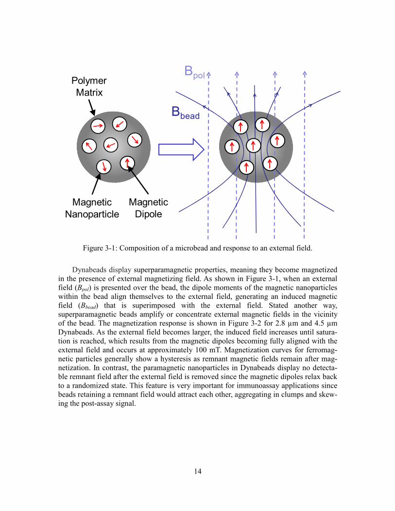
Figure 3-1: Composition of a microbead and response to an external field.
Dynabeads display superparamagnetic properties, meaning they become magnetized
in the presence of external magnetizing field. As shown in Figure 3-1, when an external
field (Bpol) is presented over the bead, the dipole moments of the magnetic nanoparticles
within the bead align themselves to the external field, generating an induced magnetic
field (Bbead) that is superimposed with the external field. Stated another way,
superparamagnetic beads amplify or concentrate external magnetic fields in the vicinity
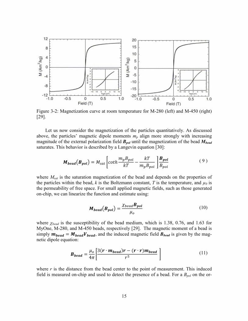
of the bead. The magnetization response is shown in Figure 3-2 for 2.8 µm and 4.5 µm
Dynabeads. As the external field becomes larger, the induced field increases until satura-
tion is reached, which results from the magnetic dipoles becoming fully aligned with the
external field and occurs at approximately 100 mT. Magnetization curves for ferromag-
netic particles generally show a hysteresis as remnant magnetic fields remain after mag-
netization. In contrast, the paramagnetic nanoparticles in Dynabeads display no detecta-
ble remnant field after the external field is removed since the magnetic dipoles relax back
to a randomized state. This feature is very important for immunoassay applications since
beads retaining a remnant field would attract each other, aggregating in clumps and skew-
ing the post-assay signal.
Bbead
BpolPolymer
Matrix
Magnetic
Nanoparticle
Magnetic
Dipole
15
Figure 3-2: Magnetization curve at room temperature for M-280 (left) and M-450 (right)
[29].
Let us now consider the magnetization of the particles quantitatively. As discussed
above, the particles’ magnetic dipole moments mp align more strongly with increasing
magnitude of the external polarization field Bpol until the magnetization of the bead Mbead
saturates. This behavior is described by a Langevin equation [30]:
)*+,-./0123 � 4��5 6789:;�<���=> ? =>;�<��� @/012<��� ( 9 )
where Msat is the saturation magnetization of the bead and depends on the properties of
the particles within the bead, k is the Boltzmann constant, T is the temperature, and µ0 is
the permeability of free space. For small applied magnetic fields, such as those generated
on-chip, we can linearize the function and estimate using:
)*+,-./0123 � A���B/012�� (10)
where χbead is the susceptibility of the bead medium, which is 1.38, 0.76, and 1.63 for
MyOne, M-280, and M-450 beads, respectively [29]. The magnetic moment of a bead is
simply C*+,- � )*+,-D*+,-, and the induced magnetic field Bbead is given by the mag-
netic dipole equation:
/*+,- � ��4F 63"H ∙ C*+,-#H ? "H ∙ H#C*+,-IJ @ (11)
where r is the distance from the bead center to the point of measurement. This induced
field is measured on-chip and used to detect the presence of a bead. For a Bpol on the or-
16
der of 1–10 mT, which are reasonable values for on-chip magnetic field generators, the
induced Bbead is approximately 1–100 µT at 3 µm away from a micron-sized magnetic
bead. For distances beyond the dimensions of the bead (e.g., 2–3 µm for 2.8 µm beads),
the magnetic field magnitude decays with K HL⁄ .
Several implications can be obtained from the above equations. First and most obvi-
ous is that larger beads have a larger magnetic moment and generate a larger Bbead. How-
ever, the size of a bead is limited by the fact that the centers of larger beads are further
away from the detectors and the effect of decaying bead field with distance eventually
cancels out the increases in bead volume. On the other hand, as was discussed in chapter
2, larger beads require a larger detection area, which is unfavorable for low-cost designs.
The second implication is that a larger Bpol produces a larger Bbead, though diminishing
returns set in at about Bpol = 10 mT and the increase in Bbead becomes negligible at Bpol >
100 mT. Increasing Bpol generally requires more power consumption in the external mag-
netic field generator or the magnetic field generator must be brought closer to the bead;
the latter approach is used in this thesis and is further explained in chapter 4. Third, it is
important for sensors to be placed as close to the beads as possible since the bead field
decays rapidly with increasing distance. This is achieved via a post-processing step de-
scribed further in chapter 4.
3.2 Magnetic label detectors
Now that the properties of magnetic beads and their induced magnetic fields have
been explained, the next step is choosing an appropriate technology for their detection.
The detector needs to convert the magnetic signal from the bead, Bbead, into an electrical
signal that indicates the presence or absence of the bead. Since our goal is a POC detector
system, we will only consider technologies that can be integrated into microchips.
The three main technologies for integrated magnetic bead detection are GMR sensors
[17], [25], [26], inductors [27], and Hall-effect sensors [11], [18], [31–35]. GMR sensors
are based on the recently discovered giant magnetoresistance effect and offer excellent
sensitivity. However, GMRs saturate at very low fields and require uniform polarization
fields to prevent saturation, which can only be reliably produced externally. Even highly
integrated external electromagnets used in conjunction with GMRs dissipate on the order
of 1 A of current [36]. Furthermore, GMRs are made using ferromagnetic materials not
standard in CMOS process and thus generally must be made on a separate chip, which
limits functionality and reduces integration. On-chip inductive sensors also offer excel-
lent sensitivity by utilizing frequency-shifting techniques and quality-factor amplifica-
tion. However, because on-chip inductors need to be tens of microns in diameter to
achieve good quality factors, their signal-to-baseline ratio is on the order of several ppm
and thus extensive calibration steps are required [27]. Further, since inductors operating
at 1 GHz are sensitive to conductive media, there exists potential interference from non-
magnetic sources. Hall-effect sensors, which are utilized in this thesis, have relatively
poor sensitivity but are robust; they are not sensitive to conductors and they can be used
in conjunction with integrated electromagnets generating non-uniform magnetic fields.
17
Further, these sensors can be scaled to several micrometers in size and arrayed to arbitrar-
ily large detection areas, which enables detection of a single bead in a very large area.
This also allows the sensors to achieve signal-to-baseline ratio on the order of 1%–10%
for magnetic microbeads using polarization detection [13] and over 100% using relaxa-
tion detection techniques [33], [34]. These detection methods are explained below.
3.3 Detection methods
Detecting the magnetic field from a bead in the presence of a much larger magnetiz-
ing field requires careful choice of a detection algorithm and associated circuitry. For ex-
ample, a typical 2.8 µm diameter bead with susceptibility χ = 1 in a 3 mT external field
generates less than 15 µT of induced field 4 µm away from the bead center. This induced
magnetic field from the bead, Bbead, is nearly 50 dB lower than the magnetizing field Bpol.
This constraint imposes stringent requirements on a detector’s dynamic range, offset, lin-
earity, and stability with respect to environmental changes.
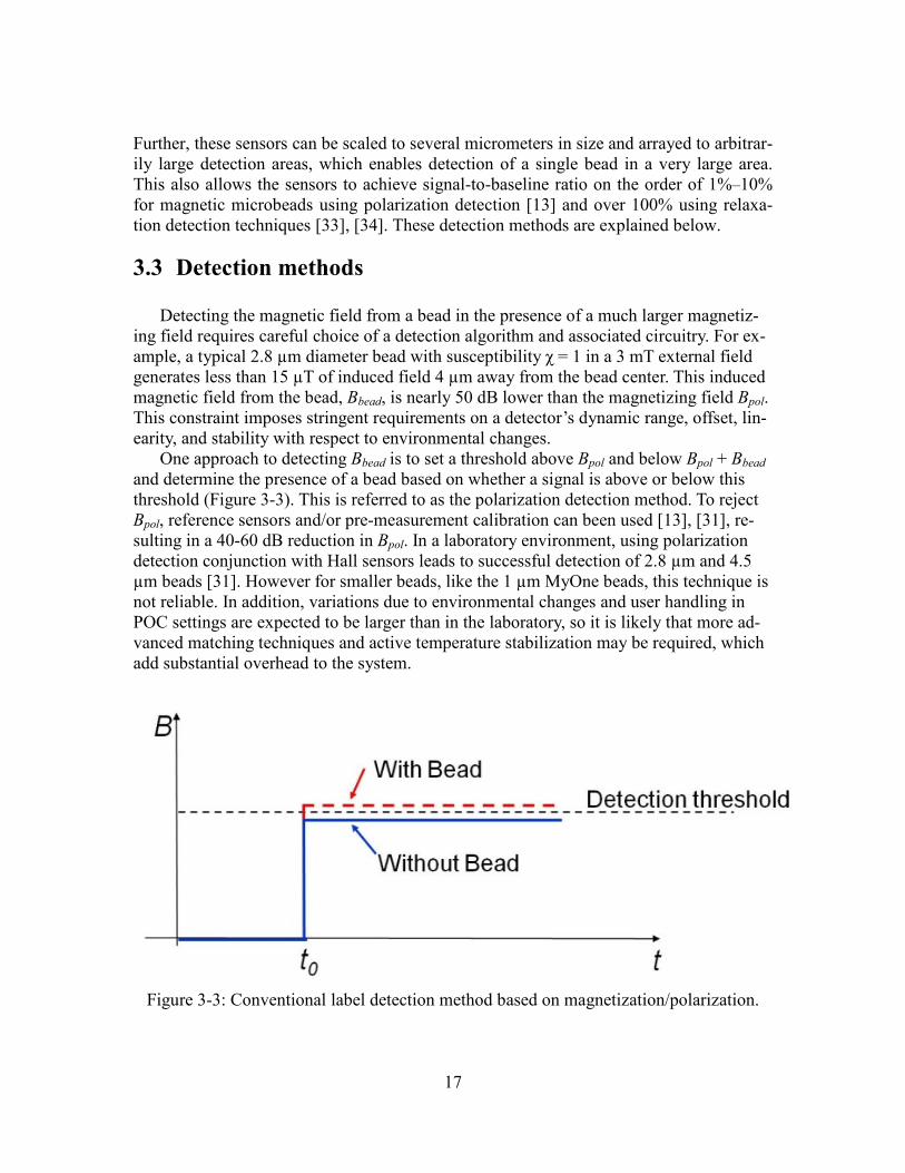
One approach to detecting Bbead is to set a threshold above Bpol and below Bpol + Bbead
and determine the presence of a bead based on whether a signal is above or below this
threshold (Figure 3-3). This is referred to as the polarization detection method. To reject
Bpol, reference sensors and/or pre-measurement calibration can been used [13], [31], re-
sulting in a 40-60 dB reduction in Bpol. In a laboratory environment, using polarization
detection conjunction with Hall sensors leads to successful detection of 2.8 µm and 4.5
µm beads [31]. However for smaller beads, like the 1 µm MyOne beads, this technique is
not reliable. In addition, variations due to environmental changes and user handling in
POC settings are expected to be larger than in the laboratory, so it is likely that more ad-
vanced matching techniques and active temperature stabilization may be required, which
add substantial overhead to the system.
Figure 3-3: Conventional label detection method based on magnetization/polarization.
18
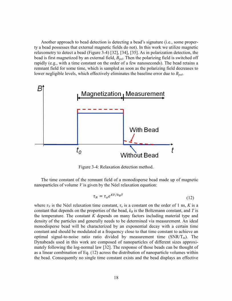
Another approach to bead detection is detecting a bead’s signature (i.e., some proper-
ty a bead possesses that external magnetic fields do not). In this work we utilize magnetic
relaxometry to detect a bead (Figure 3-4) [32], [34], [35]. As in polarization detection, the
bead is first magnetized by an external field, Bpol. Then the polarizing field is switched off
rapidly (e.g., with a time constant on the order of a few nanoseconds). The bead retains a
remnant field for some time, which is sampled as soon as the polarizing field decreases to
lower negligible levels, which effectively eliminates the baseline error due to Bpol.
Figure 3-4: Relaxation detection method.
The time constant of the remnant field of a monodisperse bead made up of magnetic
nanoparticles of volume V is given by the Néel relaxation equation:
MN � M�OPQ RST⁄ (12)
where τN is the Néel relaxation time constant, τo is a constant on the order of 1 ns, K is a
constant that depends on the properties of the bead, kB is the Boltzmann constant, and T is
the temperature. The constant K depends on many factors including material type and
density of the particles and generally needs to be determined via measurement. An ideal
monodisperse bead will be characterized by an exponential decay with a certain time
constant and should be modulated at a frequency close to that time constant to achieve an
optimal signal-to-noise ratio ratio divided by measurement time (SNR/Tm). The
Dynabeads used in this work are composed of nanoparticles of different sizes approxi-
mately following the log-normal law [32]. The response of those beads can be thought of
as a linear combination of Eq. (12) across the distribution of nanoparticle volumes within
the bead. Consequently no single time constant exists and the bead displays an effective
19
time constant that is very highly dependent on the amount of time a bead is polarized.
Thus the optimal frequency of modulation in terms of SNR/Tm is very shallow for
Dynabeads and several other bead types that were measured across frequencies from 1
kHz to 10 MHz. In practice, the frequency of modulation is chosen to be higher than the
1/f corner frequency to eliminate 1/f noise stemming from electronics and external dis-
turbances, and is on the order of 1 MHz for the system presented in chapter 5.
On-chip relaxation detection leverages the short time constants and miniaturized
components achievable in modern sub-micron CMOS technology. A 50 dB reduction in
baseline signal has been achieved this way without requiring baseline calibration or refer-
ence sensors [33]. Still, it needs to be noted that this technique is orthogonal to the cali-
bration/reference sensor techniques presented earlier; both calibration and relaxation can
be used in conjunction for even better baseline rejection [34]
3.4 Summary
Magnetic labels are ideal candidates for a POC label detector due their high preva-
lence, compatibility with integrated magnetic sensors, and high stability and signal fideli-
ty in biological environments. The beads need to be paramagnetic to prevent clumping
and thus require an external polarization field in order to be detected.
Out of several magnetic sensor technologies, we chose Hall-effect sensors due to their
compatibility with CMOS, scalability to micron-sized levels, and good robustness in
terms of specificity to magnetic fields and signal-to-baseline ratio. In order to further re-
ject the external polarization field, a relaxation detection method was developed and uti-
lized that detects a bead’s remnant relaxation signal after the polarization field is turned
off, reducing the baseline signal 300 fold.
20
4 Hall-effect bead detector design
As discussed in the previous chapters, Hall-effect sensors are can be integrated with
CMOS-technology to enable compact and low cost bead detection systems. This chapter
presents the concepts behind Hall effect and high-level design decisions made in develop-
ing the bead detector architecture and measurement algorithm. The chapter concludes
with an implementation and characterization of an 8×8 sensor test array that is used to
make more informed design decisions for a larger array presented in chapter 5.
4.1 Hall effect
The underlying principle behind Hall effect is the Lorentz force, which states that
moving electric charges experience a force in the presence of a magnetic field that is or-
thogonal to the motion of charges and the direction of the magnetic field [38]. When
charge flow is restricted to plates of conductive materials, this force manifests itself as an
electric field across the plate that can be measured using electronic means.
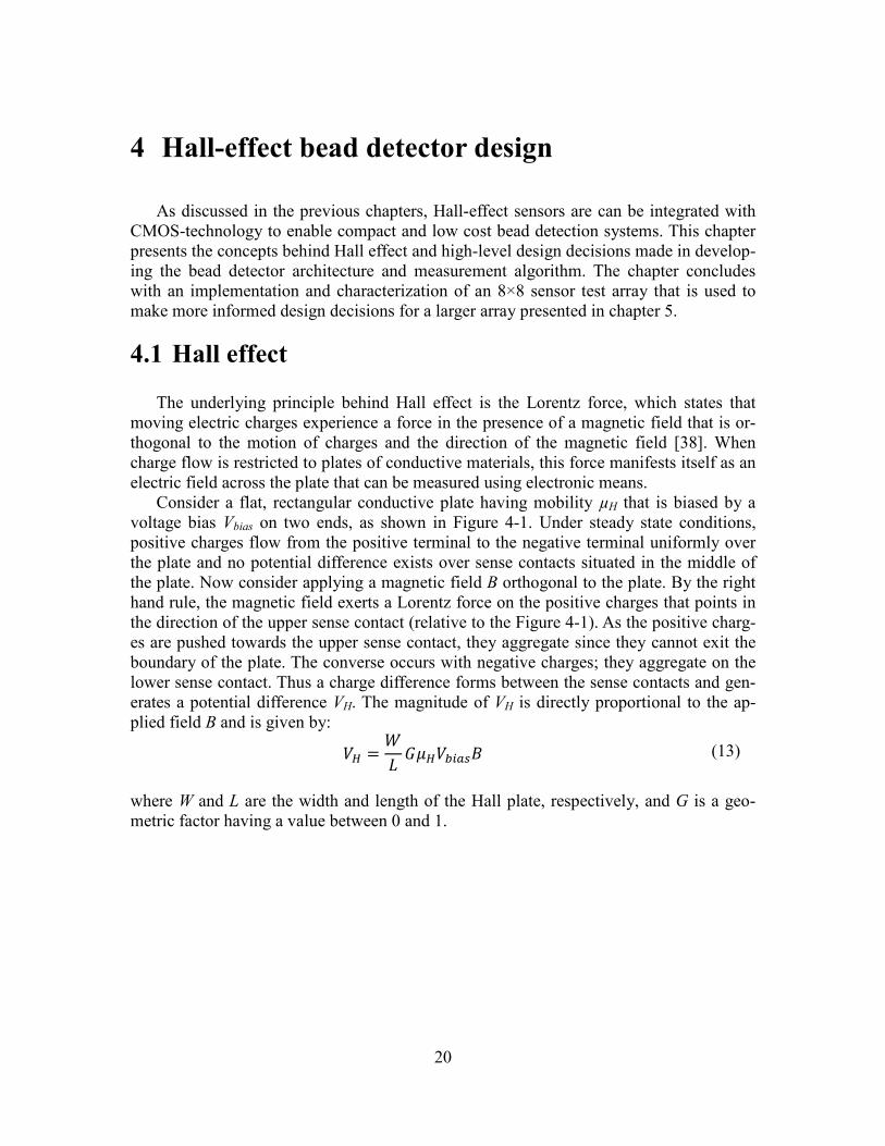
Consider a flat, rectangular conductive plate having mobility µH that is biased by a
voltage bias Vbias on two ends, as shown in Figure 4-1. Under steady state conditions,
positive charges flow from the positive terminal to the negative terminal uniformly over
the plate and no potential difference exists over sense contacts situated in the middle of
the plate. Now consider applying a magnetic field B orthogonal to the plate. By the right
hand rule, the magnetic field exerts a Lorentz force on the positive charges that points in
the direction of the upper sense contact (relative to the Figure 4-1). As the positive charg-
es are pushed towards the upper sense contact, they aggregate since they cannot exit the
boundary of the plate. The converse occurs with negative charges; they aggregate on the
lower sense contact. Thus a charge difference forms between the sense contacts and gen-
erates a potential difference VH. The magnitude of VH is directly proportional to the ap-
plied field B and is given by:
�U � VW X�U�����< (13)
where W and L are the width and length of the Hall plate, respectively, and G is a geo-
metric factor having a value between 0 and 1.
21
Figure 4-1: The principle of Hall Effect.
The sensitivity of a Hall sensor is strongly dependent on the mobility of the material.
In a standard CMOS process, Hall sensors are best realized with high mobility
semiconductive structures such as n-wells, p-wells, transistors, or diffusion resistors, as
opposed to low mobility metal plates. The sensitivity depends the term V W Y X⁄ . This
term is maximized when the Hall-effect sensor is approximately a square. Specifically, V W⁄ should be set between 0.66 and 1.2, for which V W Y X⁄ is maximum and approxi-
mately equal to 0.6 [37].
4.2 Bead detector architecture
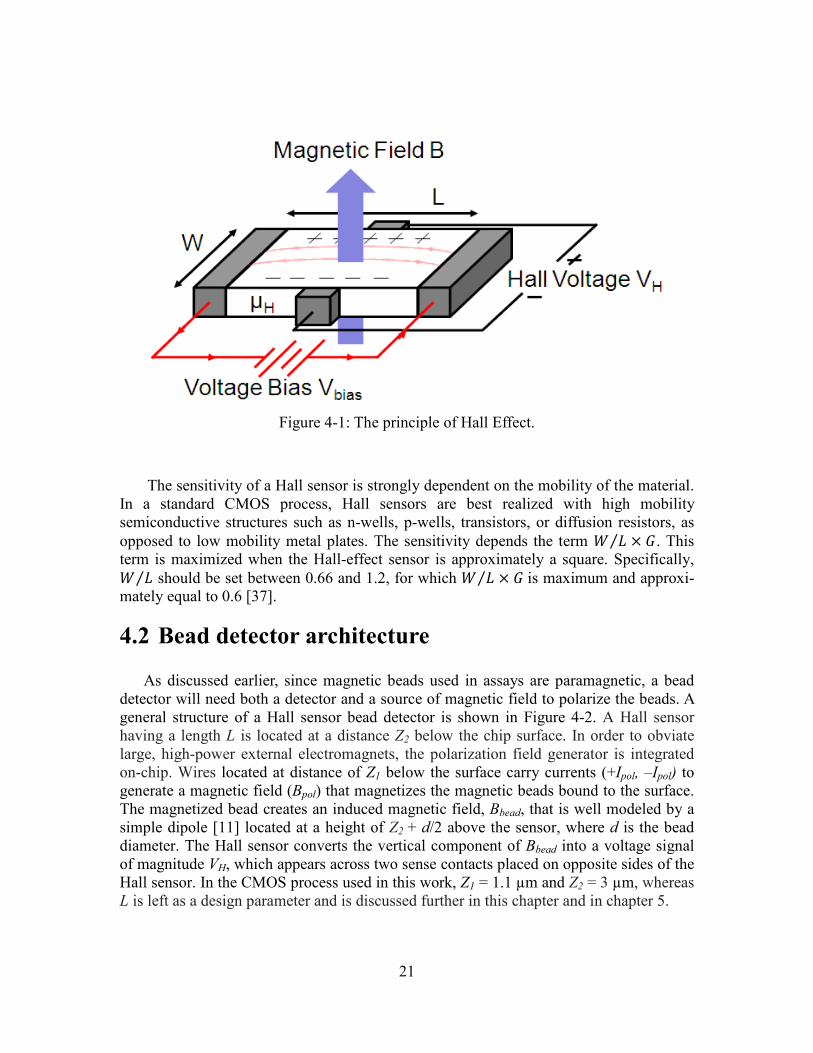
As discussed earlier, since magnetic beads used in assays are paramagnetic, a bead
detector will need both a detector and a source of magnetic field to polarize the beads. A
general structure of a Hall sensor bead detector is shown in Figure 4-2. A Hall sensor
having a length L is located at a distance Z2 below the chip surface. In order to obviate
large, high-power external electromagnets, the polarization field generator is integrated
on-chip. Wires located at distance of Z1 below the surface carry currents (+Ipol, –Ipol) to
generate a magnetic field (Bpol) that magnetizes the magnetic beads bound to the surface.
The magnetized bead creates an induced magnetic field, Bbead, that is well modeled by a
simple dipole [11] located at a height of Z2 + d/2 above the sensor, where d is the bead
diameter. The Hall sensor converts the vertical component of Bbead into a voltage signal
of magnitude VH, which appears across two sense contacts placed on opposite sides of the
Hall sensor. In the CMOS process used in this work, Z1 = 1.1 µm and Z2 = 3 µm, whereas
L is left as a design parameter and is discussed further in this chapter and in chapter 5.
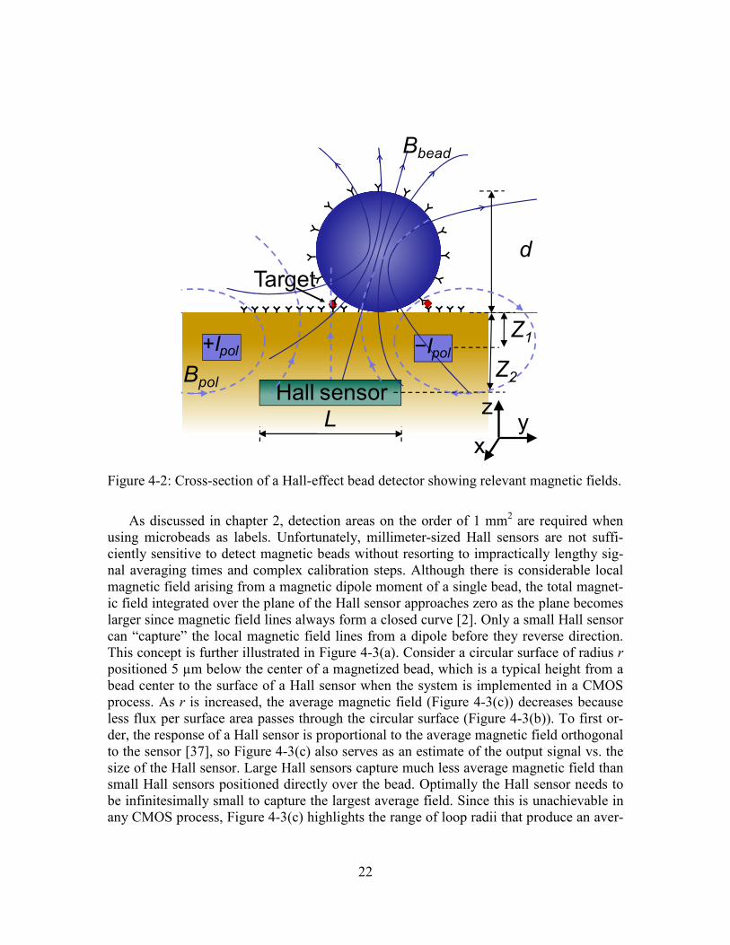
22
Figure 4-2: Cross-section of a Hall-effect bead detector showing relevant magnetic fields.
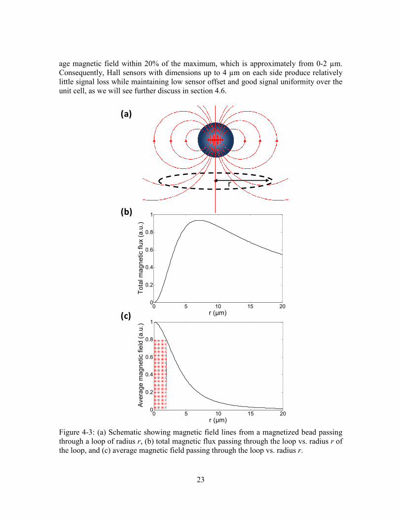
As discussed in chapter 2, detection areas on the order of 1 mm2 are required when
using microbeads as labels. Unfortunately, millimeter-sized Hall sensors are not suffi-
ciently sensitive to detect magnetic beads without resorting to impractically lengthy sig-
nal averaging times and complex calibration steps. Although there is considerable local
magnetic field arising from a magnetic dipole moment of a single bead, the total magnet-
ic field integrated over the plane of the Hall sensor approaches zero as the plane becomes
larger since magnetic field lines always form a closed curve [2]. Only a small Hall sensor
can “capture” the local magnetic field lines from a dipole before they reverse direction.
This concept is further illustrated in Figure 4-3(a). Consider a circular surface of radius r
positioned 5 µm below the center of a magnetized bead, which is a typical height from a
bead center to the surface of a Hall sensor when the system is implemented in a CMOS
process. As r is increased, the average magnetic field (Figure 4-3(c)) decreases because
less flux per surface area passes through the circular surface (Figure 4-3(b)). To first or-
der, the response of a Hall sensor is proportional to the average magnetic field orthogonal
to the sensor [37], so Figure 4-3(c) also serves as an estimate of the output signal vs. the
size of the Hall sensor. Large Hall sensors capture much less average magnetic field than
small Hall sensors positioned directly over the bead. Optimally the Hall sensor needs to
be infinitesimally small to capture the largest average field. Since this is unachievable in
any CMOS process, Figure 4-3(c) highlights the range of loop radii that produce an aver-
d
Hall sensor
+Ipol
Bbead
Bpol
L
Z1
Target
z
xy
Z2
−Ipol
23
age magnetic field within 20% of the maximum, which is approximately from 0-2 µm.
Consequently, Hall sensors with dimensions up to 4 µm on each side produce relatively
little signal loss while maintaining low sensor offset and good signal uniformity over the
unit cell, as we will see further discuss in section 4.6.
Figure 4-3: (a) Schematic showing magnetic field lines from a magnetized bead passing
through a loop of radius r, (b) total magnetic flux passing through the loop vs. radius r of
the loop, and (c) average magnetic field passing through the loop vs. radius r.
r
0 5 10 15 200
0.2
0.4
0.6
0.8
1
r (µm)
To
tal m
ag
ne
tic f
lux (
a.u
.)
0 5 10 15 200
0.2
0.4
0.6
0.8
1
r (µm)
Ave
rag
e m
ag
ne
tic f
ield
(a
.u.)
(a)
(b)
(c)
24
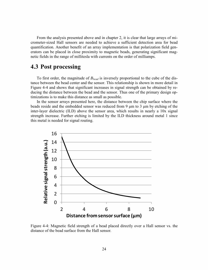
From the analysis presented above and in chapter 2, it is clear that large arrays of mi-
crometer-sized Hall sensors are needed to achieve a sufficient detection area for bead
quantification. Another benefit of an array implementation is that polarization field gen-
erators can be placed in close proximity to magnetic beads, generating significant mag-
netic fields in the range of millitesla with currents on the order of milliamps.
4.3 Post processing
To first order, the magnitude of Bbead is inversely proportional to the cube of the dis-
tance between the bead center and the sensor. This relationship is shown in more detail in
Figure 4-4 and shows that significant increases in signal strength can be obtained by re-
ducing the distance between the bead and the sensor. Thus one of the primary design op-
timizations is to make this distance as small as possible.
In the sensor arrays presented here, the distance between the chip surface where the
beads reside and the embedded sensor was reduced from 9 µm to 3 µm by etching of the
inter-layer dielectric (ILD) above the sensor area, which results in nearly a 10x signal
strength increase. Further etching is limited by the ILD thickness around metal 1 since
this metal is needed for signal routing.
Figure 4-4: Magnetic field strength of a bead placed directly over a Hall sensor vs. the
distance of the bead surface from the Hall sensor.
0
2
4
6
8
10
12
14
16
2 4 6 8 10
Re
lati
ve
sig
na
l str
en
gth
(a
.u.)
Distance from sensor surface (µm)
25
Figure 4-5 shows the post-processing flow [35]. Metallization layers, fabricated as
part of the CMOS process, were used as a hard mask for the reactive-ion etching of the
ILD. Individual chips were mounted onto a 6” wafer using photoresist and the pads of the
chip were covered with photoresist that was applied manually using a thin brush. The
photoresist was hard baked for 1 hour at 120˚C. The wafer was placed in an RIE chamber
(Centura Platform System MxP+) to remove the exposed ILD, which is a combination of
silicon oxide and silicon nitride. The chamber was filled to a pressure of 200 mTorr and
150 sccm of Ar, 15 sccm of CF4, and 45 sccm of CHF3 were introduced into the chamber.
The plasma was fired to 700 W for 30 seconds and the chamber was allowed to cool for
30 seconds afterwards. The firing of plasma and subsequent cooling was repeated ap-
proximately 40 times until all the ILD was etched off and the underlying metal 2 hard
mask was exposed, which covers the sensor region. The wafer was inspected periodically
and the process was deemed complete when no residual ILD over metal 2 was visible.
A metal wet etch was performed after the ILD etch by dipping the resulting wafer in
an aluminum etch solution (80% H3PO4, 5% HNO3, 5% CH3COOH, and 10% DI,
Transene Company Inc.) for 5 minutes to remove the metal hard mask, which brings the
chip surface another 0.5 µm closer to the Hall sensors. Subsequently, the wafers were
rinsed and a 2 minute dip in standard clean solution (5:1:1 ratio of H2O, H2O2, and
NH3OH) was performed, which removes the Ti/TiN liners and makes the sensors optical-
ly visible. The wafer was again rinsed and the photoresist was stripped using PRS-3000
(J.T. Baker) heated to 80˚C. The individual ICs were carefully removed, rinsed in DI wa-
ter, and wire bonded to a package for testing.
After post-processing, only one metal layer and one poly-silicon layer remain for
routing signals in the detection area, restricting the architecture of the polarization field
generator and the sensor cell to only these two routing layers. It is important to note that
although in this work the etching steps were performed after the CMOS process was
completed, the etching steps can be readily integrated into the CMOS process by simply
lengthening the time of the final passivation etch used to expose the pads.
26
Figure 4-5: Etching steps performed after CMOS IC fabrication to reduce the distance
between the beads and the Hall sensors; a) chip is fabricated with a metal hard mask de-
fining the sensor region; b) RIE etch is used to remove ILD over the sensor region; and c)
exposed metal layer over the sensor surface is removed with a wet etch.
4.4 Polarization field generator architecture
The magnetic moment induced on a bead is proportional to the external field Bpol. As
a result, placing polarization field generators in close proximity of the bead and increas-
ing Ipol results in a larger magnetic moment and hence larger signal. The ability to place
polarization field generators within several micrometers of the label is a critical ad-
vantage of fully integrated detectors over ones that resort to external magnets which typi-
cally consume on the order of 1 W of power [36].
27
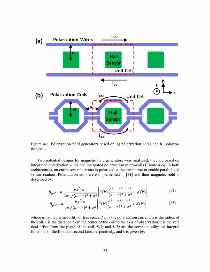
Figure 4-6: Polarization field generators based on: a) polarization wires and b) polariza-
tion coils.
Two potential designs for magnetic field generators were analyzed; they are based on
integrated polarization wires and integrated polarization micro-coils (Figure 4-6). In both
architectures, an entire row of sensors is polarized at the same time to enable parallelized
sensor readout. Polarization coils were implemented in [31] and their magnetic field is
described by:
<���,[ � ��\���]2FI_"` � I#� � ]� 6a"=# `� � I� � ]�"` ? I#� � ]� ? b"=#@ (14)
<���,c � ��\���2F_"` � I#� � ]� 6a"=# `� ? I� ? ]�"` ? I#� � ]� � b"=#@ (15)
where µo is the permeability of free space, Ipol is the polarization current, a is the radius of
the coil, r is the distance from the center of the coil to the axis of observation, z is the ver-
tical offset from the plane of the coil, E(k) and K(k) are the complete elliptical integral
functions of the first and second kind, respectively, and k is given by:
Hall
Sensor
Hall
Sensor
Polarization Wires
Polarization Coils x
y
Unit Cell
Unit Cell
Ipol
Ipol
Ipol
Ipol
z
a
aa
(a)
(b)
28
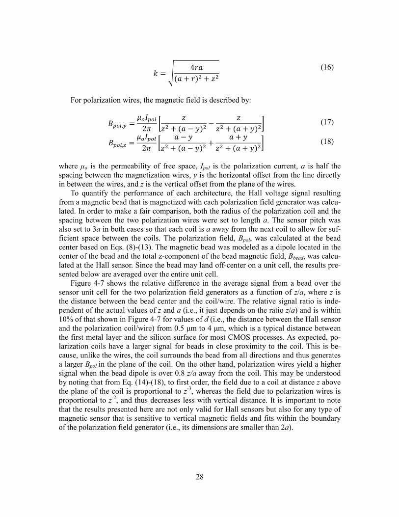
= � d 4I`"` � I#� � ]� (16)
For polarization wires, the magnetic field is described by:
<���,e � ��\���2F f ]]� � "` ? g#� ? ]]� � "` � g#�h (17)
<���,c � ��\���2F f ` ? g]� � "` ? g#� � ` � g]� � "` � g#�h (18)
where µo is the permeability of free space, Ipol is the polarization current, a is half the
spacing between the magnetization wires, y is the horizontal offset from the line directly
in between the wires, and z is the vertical offset from the plane of the wires.
To quantify the performance of each architecture, the Hall voltage signal resulting
from a magnetic bead that is magnetized with each polarization field generator was calcu-
lated. In order to make a fair comparison, both the radius of the polarization coil and the
spacing between the two polarization wires were set to length a. The sensor pitch was
also set to 3a in both cases so that each coil is a away from the next coil to allow for suf-
ficient space between the coils. The polarization field, Bpol, was calculated at the bead
center based on Eqs. (8)-(13). The magnetic bead was modeled as a dipole located in the
center of the bead and the total z-component of the bead magnetic field, Bbead, was calcu-
lated at the Hall sensor. Since the bead may land off-center on a unit cell, the results pre-
sented below are averaged over the entire unit cell.
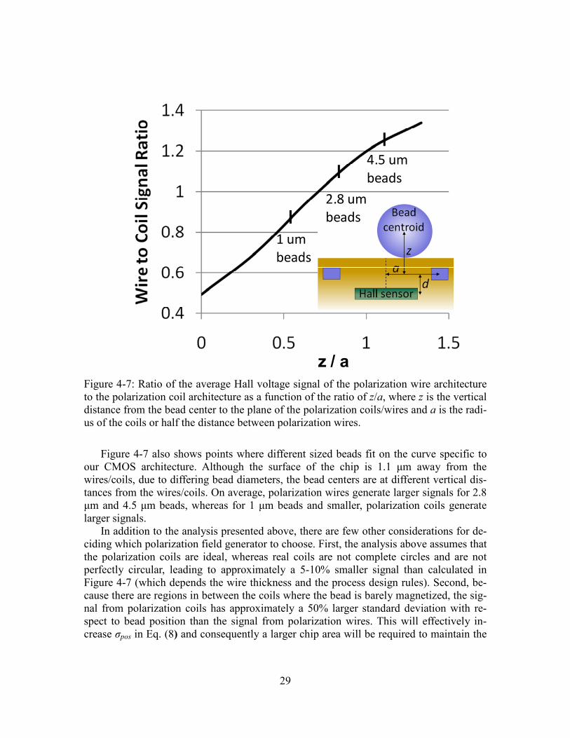
Figure 4-7 shows the relative difference in the average signal from a bead over the
sensor unit cell for the two polarization field generators as a function of z/a, where z is
the distance between the bead center and the coil/wire. The relative signal ratio is inde-
pendent of the actual values of z and a (i.e., it just depends on the ratio z/a) and is within
10% of that shown in Figure 4-7 for values of d (i.e., the distance between the Hall sensor
and the polarization coil/wire) from 0.5 µm to 4 µm, which is a typical distance between
the first metal layer and the silicon surface for most CMOS processes. As expected, po-
larization coils have a larger signal for beads in close proximity to the coil. This is be-
cause, unlike the wires, the coil surrounds the bead from all directions and thus generates
a larger Bpol in the plane of the coil. On the other hand, polarization wires yield a higher
signal when the bead dipole is over 0.8 z/a away from the coil. This may be understood
by noting that from Eq. (14)-(18), to first order, the field due to a coil at distance z above
the plane of the coil is proportional to z-3
, whereas the field due to polarization wires is
proportional to z-2
, and thus decreases less with vertical distance. It is important to note
that the results presented here are not only valid for Hall sensors but also for any type of
magnetic sensor that is sensitive to vertical magnetic fields and fits within the boundary
of the polarization field generator (i.e., its dimensions are smaller than 2a).
29
Figure 4-7: Ratio of the average Hall voltage signal of the polarization wire architecture
to the polarization coil architecture as a function of the ratio of z/a, where z is the vertical
distance from the bead center to the plane of the polarization coils/wires and a is the radi-
us of the coils or half the distance between polarization wires.
Figure 4-7 also shows points where different sized beads fit on the curve specific to
our CMOS architecture. Although the surface of the chip is 1.1 µm away from the
wires/coils, due to differing bead diameters, the bead centers are at different vertical dis-
tances from the wires/coils. On average, polarization wires generate larger signals for 2.8
µm and 4.5 µm beads, whereas for 1 µm beads and smaller, polarization coils generate
larger signals.
In addition to the analysis presented above, there are few other considerations for de-
ciding which polarization field generator to choose. First, the analysis above assumes that
the polarization coils are ideal, whereas real coils are not complete circles and are not
perfectly circular, leading to approximately a 5-10% smaller signal than calculated in
Figure 4-7 (which depends the wire thickness and the process design rules). Second, be-
cause there are regions in between the coils where the bead is barely magnetized, the sig-
nal from polarization coils has approximately a 50% larger standard deviation with re-
spect to bead position than the signal from polarization wires. This will effectively in-
crease σpos in Eq. (8) and consequently a larger chip area will be required to maintain the
4.5 um
beads
1 um
beads
2.8 um
beads
z / a
30
same detector system accuracy. Third, polarization coils have approximately a 30%
greater resistance per unit cell and thus they can polarize only about 70% of the sensors
that can be polarized with polarization wires at a given supply voltage. Thus detection
will be approximately 30% slower using coils rather than wires. Fourth, polarization
wires can be shared among different rows (i.e., the top wire of one row may be used as a
bottom wire of the row above it), whereas this is not feasible with polarization coils. Sep-
arate coils would need to be implemented for each row, taking up approximately 10–30%
more area. Lastly, it is easier to route other signals (e.g., supply and ground lines, word
lines, etc.) next to the straight wires in the polarization wire architecture than the curving
coils in the polarization coil architecture, leading to a less complex layout.
Given the results Figure 4-7 and the arguments presented above, polarization wires
are preferable for detecting large beads and in general are more practical to implement in
the CMOS process. Consequently, the polarization wire magnetic field generator was se-
lected for the arrays presented in this thesis.
4.5 Sensor non-idealities and measurement algorithm
As discussed earlier, the magnetic bead signal Bbead is relatively small (around 10–100
µT) and can be corrupted by various sources of errors such as variations from sensors,
circuitry, and the environment. In this section, we outline these error sources and present
a measurement algorithm that significantly attenuates them.
First, miniaturized Hall sensors have an intrinsic offset that is on the order of 1% of
Vbias (e.g., approximately 20 mV for a 2 V bias voltage) for the CMOS process used in
this work. The equivalent input referred offset can be as large as 300 mT, over 10,000
times higher than the smallest bead signal we want to detect. Further contributing to the
low frequency offset are interference from DC magnetic fields such as the Earth’s field
(~50 µT) and AC magnetic fields such as those from power lines and urban noise, but
these error sources are significantly smaller.
Second, in the case polarization currents are switched on and off (which is the case
for relaxation detection shown in Figure 3-4), substantial heating can occur in the current
lines that generates temperature gradients over the sensors. Figure 4-8 (a) and (b) show
simulation of temperature rise due to a polarization current of 32 mA flowing through the
polarization wires. Specifically, Figure 4-8(a) shows a cross section displaying steady
state temperature changes when the polarization line is turned on and Figure 4-8(b)
shows a top view of an entire row of sensors displaying the temperature changes of the
silicon substrate (where the Hall sensors lie). The highest gradients occur at the edges of
the row where the polarization wires terminate and the heating effect stops (in reality the
wires are routed to a much wider and higher level metal, which generates substantially
less heat on the silicon). These temperature gradients manifest themselves as voltages on
the Hall sensors via thermo-electric effects. Specifically, in silicon, the thermopower co-
efficient is 0.5 mV/K or about 8 mT/K when input referred to the magnetic field over
Hall sensors. Thus a gradient of 1/1000 of a Celsius over a n-well Hall sensor can create
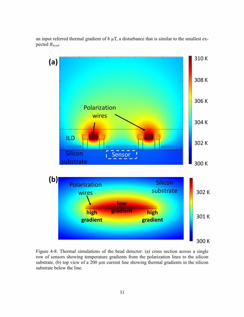
31
an input referred thermal gradient of 8 µT, a disturbance that is similar to the smallest ex-
pected Bbead.
Figure 4-8: Thermal simulations of the bead detector: (a) cross section across a single
row of sensors showing temperature gradients from the polarization lines to the silicon
substrate, (b) top view of a 200 µm current line showing thermal gradients in the silicon
substrate below the line.
300 K
302 K
304 K
306 K
308 K
310 K
Sensor
Polarization
wires
high
gradient
high
gradient
low
gradient
300 K
301 K
302 K
(a)
(b)Polarization
wires
Silicon
substrate
Silicon
substrate
ILD
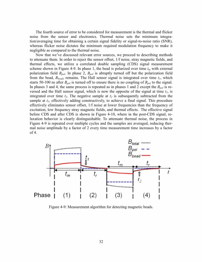
32
The fourth source of error to be considered for measurement is the thermal and flicker
noise from the sensor and electronics. Thermal noise sets the minimum integra-
tion/averaging time for obtaining a certain signal fidelity or signal-to-noise ratio (SNR),
whereas flicker noise dictates the minimum required modulation frequency to make it
negligible as compared to the thermal noise.
Now that we’ve discussed relevant error sources, we proceed to describing methods
to attenuate them. In order to reject the sensor offset, 1/f noise, stray magnetic fields, and
thermal effects, we utilize a correlated double sampling (CDS) signal measurement
scheme shown in Figure 4-9. In phase 1, the bead is polarized over time tm with external
polarization field Bpol. In phase 2, Bpol is abruptly turned off but the polarization field
from the bead, Bbead, remains. The Hall sensor signal is integrated over time t1, which
starts 50-100 ns after Bpol is turned off to ensure there is no coupling of Bpol to the signal.
In phases 3 and 4, the same process is repeated as in phases 1 and 2 except the Bpol is re-
versed and the Hall sensor signal, which is now the opposite of the signal at time t1, is
integrated over time t2. The negative sample at t2 is subsequently subtracted from the
sample at t1, effectively adding constructively, to achieve a final signal. This procedure
effectively eliminates sensor offset, 1/f noise at lower frequencies than the frequency of
excitation, low frequency stray magnetic fields, and thermal effects. The effective signal
before CDS and after CDS is shown in Figure 4-10, where in the post-CDS signal, re-
laxation behavior is clearly distinguishable. To attenuate thermal noise, the process in
Figure 4-9 is repeated over multiple cycles and the samples are averaged, reducing ther-
mal noise amplitude by a factor of 2 every time measurement time increases by a factor
of 4.
Figure 4-9: Measurement algorithm for detecting magnetic beads.
33
Figure 4-10: Example of a signal before CDS (blue) including both offset and thermal
effects and after CDS (red), where DC offset and thermal effects are cancelled.
4.6 Test array implementation and results
In order to test the Hall sensor bead detector and compare two Hall sensor plate types,
one using an n-well and the other using a MOS active region, 8×8 sensor arrays were de-
signed and implemented in the 0.18 µm CMOS process. Figure 4-11 shows the unit cell
architecture for each implementation. Each unit cell contains a Hall plate, bias wires, po-
larization wires, signal bit lines, and, in the n-well implementation, access transistors sim-
ilar to those in SRAM.
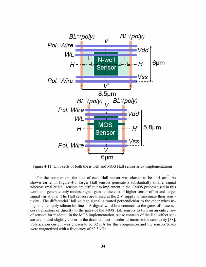
34
Figure 4-11: Unit-cells of both the n-well and MOS Hall sensor array implementations.
For the comparison, the size of each Hall sensor was chosen to be 4×4 µm2. As
shown earlier in Figure 4-3, larger Hall sensors generate a substantially smaller signal
whereas smaller Hall sensors are difficult to implement in the CMOS process used in this
work and generate only modest signal gains at the cost of higher sensor offset and larger
signal variations. The Hall sensors are biased at the 2 V supply to maximize their sensi-
tivity. The differential Hall voltage signal is routed perpendicular to the other wires us-
ing silicided poly-silicon bit lines. A digital word line connects to the gates of these ac-
cess transistors or directly to the gates of the MOS Hall sensors to turn on an entire row
of sensors for readout. In the MOS implementation, sense contacts of the Hall-effect sen-
sor are placed slightly closer to the drain contact in order to increase the sensitivity [38].
Polarization current was chosen to be 32 mA for this comparison and the sensors/beads
were magnetized with a frequency of 62.5 kHz.
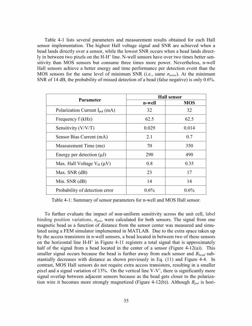
35
Table 4-1 lists several parameters and measurement results obtained for each Hall
sensor implementation. The highest Hall voltage signal and SNR are achieved when a
bead lands directly over a sensor, while the lowest SNR occurs when a bead lands direct-
ly in between two pixels on the H-H’ line. N-well sensors have over two times better sen-
sitivity than MOS sensors but consume three times more power. Nevertheless, n-well
Hall sensors achieve a better energy and time performance per detection event than the
MOS sensors for the same level of minimum SNR (i.e., same σnoise). At the minimum
SNR of 14 dB, the probability of missed detection of a bead (false negative) is only 0.6%.
Parameter Hall sensor
n-well MOS
Polarization Current Ipol (mA) 32 32
Frequency f (kHz) 62.5 62.5
Sensitivity (V/V/T) 0.029 0.014
Sensor Bias Current (mA) 2.1 0.7
Measurement Time (ms) 70 350
Energy per detection (µJ) 290 490
Max. Hall Voltage VH (µV) 0.8 0.35
Max. SNR (dB) 23 17
Min. SNR (dB) 14 14
Probability of detection error 0.6% 0.6%
Table 4-1: Summary of sensor parameters for n-well and MOS Hall sensor.
To further evaluate the impact of non-uniform sensitivity across the unit cell, label
binding position variations, σpos, were calculated for both sensors. The signal from one
magnetic bead as a function of distance from the sensor center was measured and simu-
lated using a FEM simulator implemented in MATLAB. Due to the extra space taken up
by the access transistors in n-well sensors, a bead located in between two of these sensors
on the horizontal line H-H’ in Figure 4-11 registers a total signal that is approximately
half of the signal from a bead located in the center of a sensor (Figure 4-12(a)). This
smaller signal occurs because the bead is further away from each sensor and Bbead sub-
stantially decreases with distance as shown previously in Eq. (11) and Figure 4-4. In
contrast, MOS Hall sensors do not require extra access transistors, resulting in a smaller
pixel and a signal variation of 13%. On the vertical line V-V’, there is significantly more
signal overlap between adjacent sensors because as the bead gets closer to the polariza-
tion wire it becomes more strongly magnetized (Figure 4-12(b)). Although Bpol is hori-
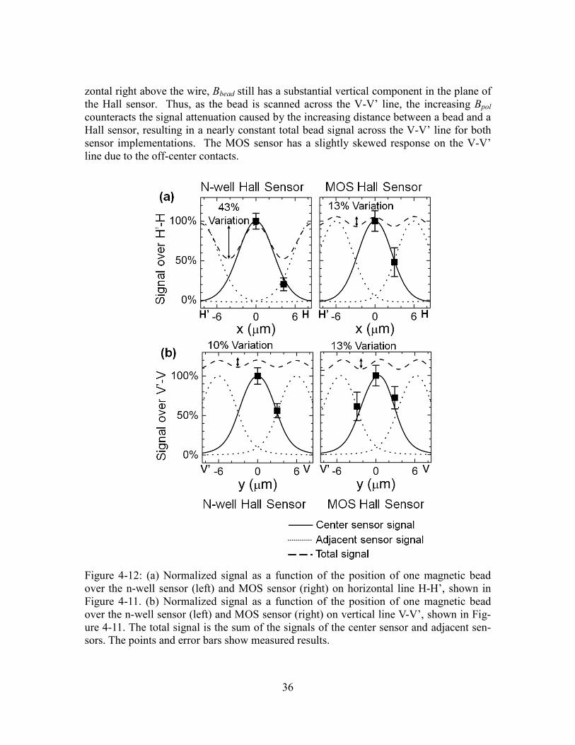
36
zontal right above the wire, Bbead still has a substantial vertical component in the plane of
the Hall sensor. Thus, as the bead is scanned across the V-V’ line, the increasing Bpol
counteracts the signal attenuation caused by the increasing distance between a bead and a
Hall sensor, resulting in a nearly constant total bead signal across the V-V’ line for both
sensor implementations. The MOS sensor has a slightly skewed response on the V-V’
line due to the off-center contacts.
Figure 4-12: (a) Normalized signal as a function of the position of one magnetic bead
over the n-well sensor (left) and MOS sensor (right) on horizontal line H-H’, shown in
Figure 4-11. (b) Normalized signal as a function of the position of one magnetic bead
over the n-well sensor (left) and MOS sensor (right) on vertical line V-V’, shown in Fig-
ure 4-11. The total signal is the sum of the signals of the center sensor and adjacent sen-
sors. The points and error bars show measured results.
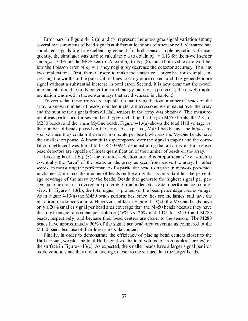
37
Error bars in Figure 4-12 (a) and (b) represent the one-sigma signal variation among
several measurements of bead signals at different locations of a sensor cell. Measured and
simulated signals are in excellent agreement for both sensor implementations. Conse-
quently, the simulator was used to calculate σpol to obtain σpol = 0.13 for the n-well sensor
and σpol = 0.06 for the MOS sensor. According to Eq. (8), since both values are well be-
low the Poisson error of σP = 1, they negligibly decrease the detector accuracy. This has
two implications. First, there is room to make the sensor cell larger by, for example, in-
creasing the widths of the polarization lines to carry more current and thus generate more
signal without a substantial increase in total error. Second, it is now clear that the n-well
implementation, due to its better time and energy metrics, is preferred; the n-well imple-
mentation was used in the sensor arrays that are discussed in chapter 5.
To verify that these arrays are capable of quantifying the total number of beads on the
array, a known number of beads, counted under a microscope, were placed over the array
and the sum of the signals from all Hall sensors in the array was obtained. This measure-
ment was performed for several bead types including the 4.5 µm M450 beads, the 2.8 µm
M280 beads, and the 1 µm MyOne beads. Figure 4-13(a) shows the total Hall voltage vs.
the number of beads placed on the array. As expected, M450 beads have the largest re-
sponse since they contain the most iron oxide per bead, whereas the MyOne beads have
the smallest response. A linear fit is superimposed over the signal samples and the corre-
lation coefficient was found to be R > 0.997, demonstrating that an array of Hall sensor
bead detectors are capable of linear quantification of the number of beads on the array.
Looking back at Eq. (8), the required detection area A is proportional d2×n, which is
essentially the “area” of the beads on the array as seen from above the array. In other
words, in measuring the performance of a particular bead using the framework presented
in chapter 2, it is not the number of beads on the array that is important but the percent-
age coverage of the array by the beads. Beads that generate the highest signal per per-
centage of array area covered are preferable from a detector system performance point of
view. In Figure 4-13(b), the total signal is plotted vs. the bead percentage area coverage.
As in Figure 4-13(a) the M450 beads perform best since they are the largest and have the
most iron oxide per volume. However, unlike in Figure 4-13(a), the MyOne beads have
only a 20% smaller signal per bead area coverage than the M450 beads because they have
the most magnetic content per volume (26% vs. 20% and 14% for M450 and M280
beads, respectively) and because their bead centers are closer to the sensors. The M280
beads have approximately 50% of the signal per bead area coverage as compared to the
M450 beads because of their low iron oxide content.
Finally, in order to demonstrate the efficiency of placing bead centers closer to the
Hall sensors, we plot the total Hall signal vs. the total volume of iron oxides (ferrites) on
the surface in Figure 4-13(c). As expected, the smaller beads have a larger signal per iron
oxide volume since they are, on average, closer to the surface than the larger beads.
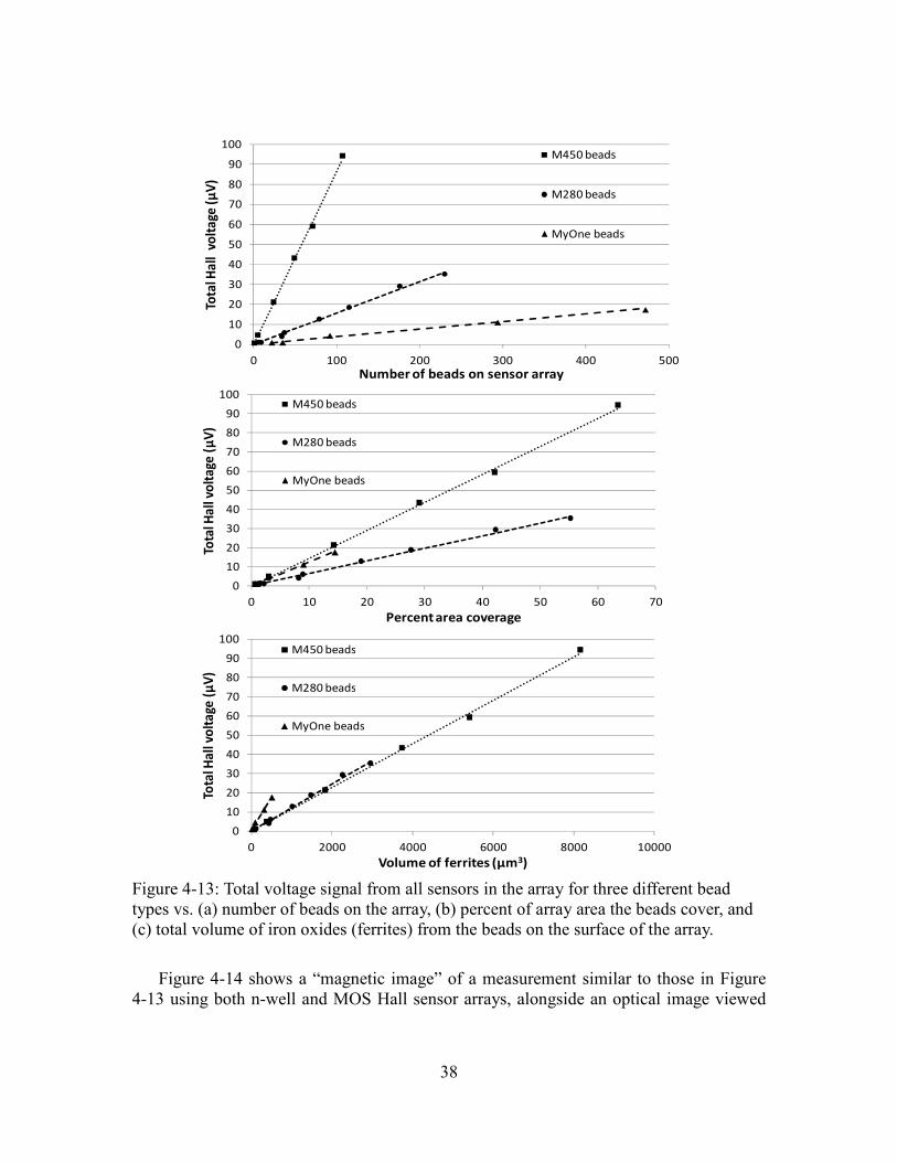
38
Figure 4-13: Total voltage signal from all sensors in the array for three different bead
types vs. (a) number of beads on the array, (b) percent of array area the beads cover, and
(c) total volume of iron oxides (ferrites) from the beads on the surface of the array.
Figure 4-14 shows a “magnetic image” of a measurement similar to those in Figure
4-13 using both n-well and MOS Hall sensor arrays, alongside an optical image viewed
0
10
20
30
40
50
60
70
80
90
100
0 100 200 300 400 500
Tota
l Ha
ll v
olt
age
(μ
V)
Number of beads on sensor array
M450 beads
M280 beads
MyOne beads
0
10
20
30
40
50
60
70
80
90
100
0 10 20 30 40 50 60 70
Tota
l Ha
ll v
olt
age
(μ
V)
Percent area coverage
M450 beads
M280 beads
MyOne beads
0
10
20
30
40
50
60
70
80
90
100
0 2000 4000 6000 8000 10000
Tota
l Ha
ll v
olt
age
(μ
V)
Volume of ferrites (µm3)
M450 beads
M280 beads
MyOne beads
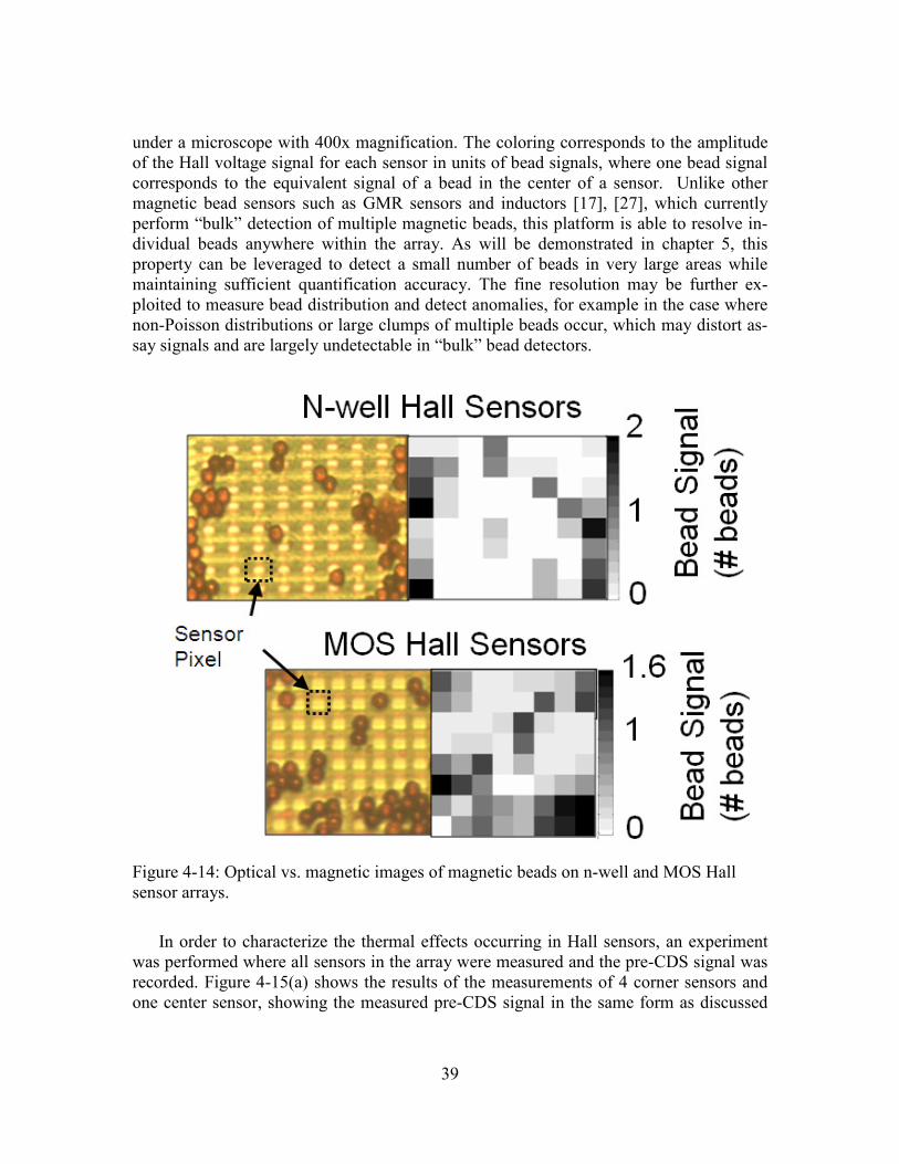
39
under a microscope with 400x magnification. The coloring corresponds to the amplitude
of the Hall voltage signal for each sensor in units of bead signals, where one bead signal
corresponds to the equivalent signal of a bead in the center of a sensor. Unlike other
magnetic bead sensors such as GMR sensors and inductors [17], [27], which currently
perform “bulk” detection of multiple magnetic beads, this platform is able to resolve in-
dividual beads anywhere within the array. As will be demonstrated in chapter 5, this
property can be leveraged to detect a small number of beads in very large areas while
maintaining sufficient quantification accuracy. The fine resolution may be further ex-
ploited to measure bead distribution and detect anomalies, for example in the case where
non-Poisson distributions or large clumps of multiple beads occur, which may distort as-
say signals and are largely undetectable in “bulk” bead detectors.
Figure 4-14: Optical vs. magnetic images of magnetic beads on n-well and MOS Hall
sensor arrays.
In order to characterize the thermal effects occurring in Hall sensors, an experiment
was performed where all sensors in the array were measured and the pre-CDS signal was
recorded. Figure 4-15(a) shows the results of the measurements of 4 corner sensors and
one center sensor, showing the measured pre-CDS signal in the same form as discussed
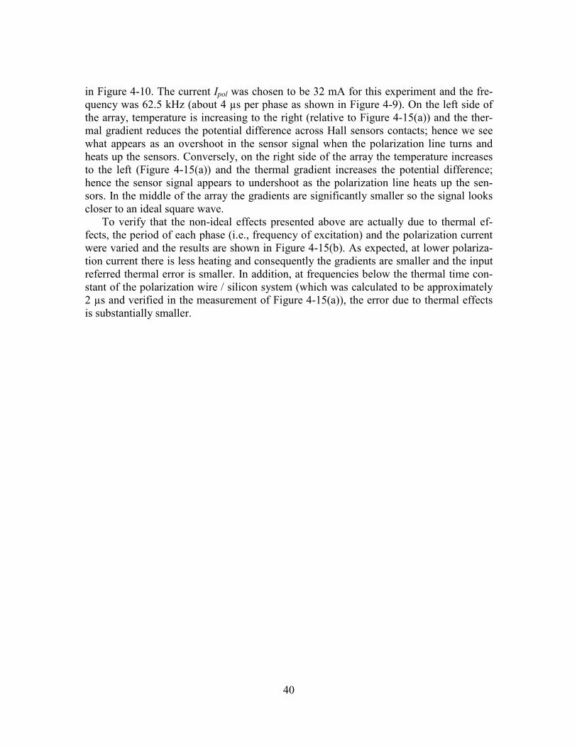
40
in Figure 4-10. The current Ipol was chosen to be 32 mA for this experiment and the fre-
quency was 62.5 kHz (about 4 µs per phase as shown in Figure 4-9). On the left side of
the array, temperature is increasing to the right (relative to Figure 4-15(a)) and the ther-
mal gradient reduces the potential difference across Hall sensors contacts; hence we see
what appears as an overshoot in the sensor signal when the polarization line turns and
heats up the sensors. Conversely, on the right side of the array the temperature increases
to the left (Figure 4-15(a)) and the thermal gradient increases the potential difference;
hence the sensor signal appears to undershoot as the polarization line heats up the sen-
sors. In the middle of the array the gradients are significantly smaller so the signal looks
closer to an ideal square wave.
To verify that the non-ideal effects presented above are actually due to thermal ef-
fects, the period of each phase (i.e., frequency of excitation) and the polarization current
were varied and the results are shown in Figure 4-15(b). As expected, at lower polariza-
tion current there is less heating and consequently the gradients are smaller and the input
referred thermal error is smaller. In addition, at frequencies below the thermal time con-
stant of the polarization wire / silicon system (which was calculated to be approximately
2 µs and verified in the measurement of Figure 4-15(a)), the error due to thermal effects
is substantially smaller.
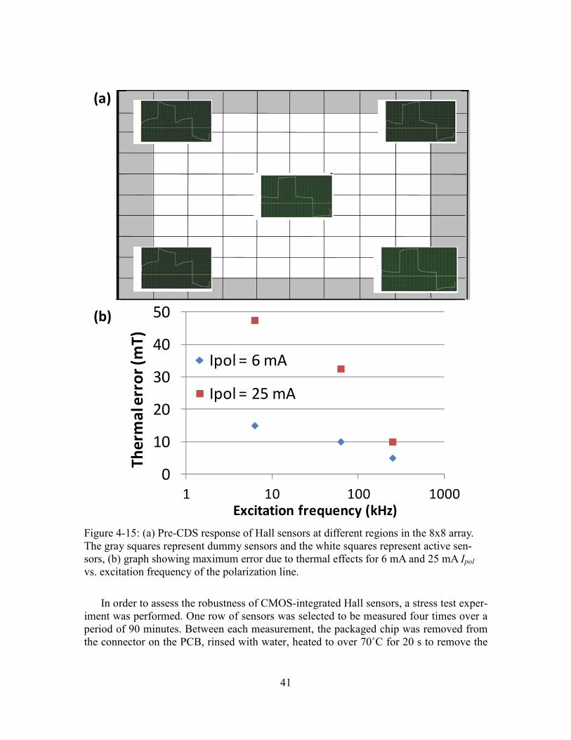
41
Figure 4-15: (a) Pre-CDS response of Hall sensors at different regions in the 8x8 array.
The gray squares represent dummy sensors and the white squares represent active sen-
sors, (b) graph showing maximum error due to thermal effects for 6 mA and 25 mA Ipol
vs. excitation frequency of the polarization line.
In order to assess the robustness of CMOS-integrated Hall sensors, a stress test exper-
iment was performed. One row of sensors was selected to be measured four times over a
period of 90 minutes. Between each measurement, the packaged chip was removed from
the connector on the PCB, rinsed with water, heated to over 70˚C for 20 s to remove the
(a)
(b)
0
10
20
30
40
50
1 10 100
Th
erm
al e
rro
r (m
T)
Excitation period T (µs)
Ipol = 6 mA
Ipol = 25 mA
0
10
20
30
40
50
1 10 100 1000
Th
erm
al e
rro
r (m
T)
Excitation frequency (kHz)
Ipol = 6 mA
Ipol = 25 mA
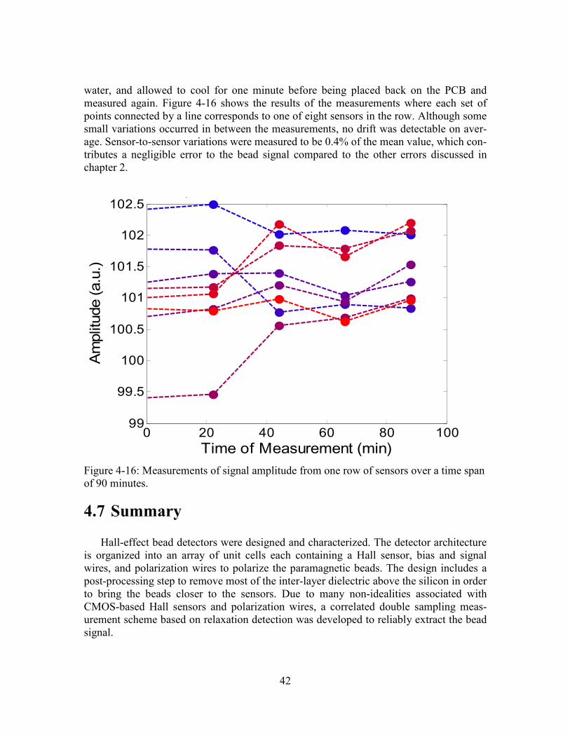
42
water, and allowed to cool for one minute before being placed back on the PCB and
measured again. Figure 4-16 shows the results of the measurements where each set of
points connected by a line corresponds to one of eight sensors in the row. Although some
small variations occurred in between the measurements, no drift was detectable on aver-
age. Sensor-to-sensor variations were measured to be 0.4% of the mean value, which con-
tributes a negligible error to the bead signal compared to the other errors discussed in
chapter 2.
Figure 4-16: Measurements of signal amplitude from one row of sensors over a time span
of 90 minutes.
4.7 Summary
Hall-effect bead detectors were designed and characterized. The detector architecture
is organized into an array of unit cells each containing a Hall sensor, bias and signal
wires, and polarization wires to polarize the paramagnetic beads. The design includes a
post-processing step to remove most of the inter-layer dielectric above the silicon in order
to bring the beads closer to the sensors. Due to many non-idealities associated with
CMOS-based Hall sensors and polarization wires, a correlated double sampling meas-
urement scheme based on relaxation detection was developed to reliably extract the bead
signal.
0 20 40 60 80 10099
99.5
100
100.5
101
101.5
102
102.5Amplitude vs. Time of Measurement
Time of Measurement (min)
Am
plit
ude (a.u
.)
43
To validate the proposed bead detector architecture, measurement scheme, and to
chose an appropriate type of Hall sensor, small arrays of n-well based and MOS transistor
based Hall sensors were fabricated and characterized. Due to their superior sensitivity,
the n-well sensors were chosen for further consideration and analysis. These sensors
show a linear relationship between the number of beads and total signal and are able to
resolve individual beads in the array. Further, the sensors show very little sensor-to-
sensor variation and display no significant drift after being thermally and mechanically
stressed.
44
5 Bead detector array
This chapter extends the bead detector design of chapter 4 to larger arrays derived
with the design framework presented in chapter 2. Considerations for optimizing the per-
formance of the bead array are first presented. Subsequently, the design of the readout
circuitry is explained. The chapter concludes with an implementation and characterization
of a 10,240 sensor array that can detect magnetic bead labels with sufficient accuracy and
dynamic range for use in diagnostic applications.
5.1 Array design and optimization
Figure 5-1 shows the architecture of the Hall sensor array implemented in this chap-
ter. Switches at the sides of the array connect one row of sensors to the supply lines (Vdd
= 2 V and ground = 0 V) while another set of switches (not shown) turn on the current in
the polarization wires next to the enabled sensors to magnetize beads in their vicinity.
The supply lines and polarization lines are shared between adjacent rows to minimize IR
drop and increase sensor packing density. The word line is enabled to transfer sensor sig-
nal to the bit-lines that carry the signals to the top and bottom of the array to be digitized
in parallel by a series of pitch-matched amplifiers and digitizers [35]. The array can be
trivially scaled by utilizing multiple array banks or by adding more rows to the array (up
to a limit of 64 due to thermal noise coming from the high resistance poly bit lines). The
main design challenge thus lies in designing the individual row of sensors that makes up
the array.
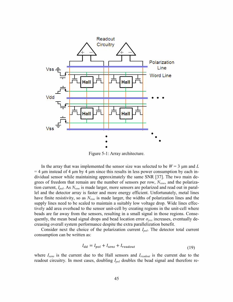
45
Figure 5-1: Array architecture.
In the array that was implemented the sensor size was selected to be W = 3 µm and L
= 4 µm instead of 4 µm by 4 µm since this results in less power consumption by each in-
dividual sensor while maintaining approximately the same SNR [37]. The two main de-
grees of freedom that remain are the number of sensors per row, Nrow, and the polariza-
tion current, Ipol. As Nrow is made larger, more sensors are polarized and read out in paral-
lel and the detector array is faster and more energy efficient. Unfortunately, metal lines
have finite resistivity, so as Nrow is made larger, the widths of polarization lines and the
supply lines need to be scaled to maintain a suitably low voltage drop. Wide lines effec-
tively add area overhead to the sensor unit-cell by creating regions in the unit-cell where
beads are far away from the sensors, resulting in a small signal in those regions. Conse-
quently, the mean bead signal drops and bead location error σpos increases, eventually de-
creasing overall system performance despite the extra parallelization benefit.
Consider next the choice of the polarization current Ipol. The detector total current
consumption can be written as:
\BB � \��� � \��!� � \[��B�i5 (19)
where Isens is the current due to the Hall sensors and Ireadout is the current due to the
readout circuitry. In most cases, doubling Ipol doubles the bead signal and therefore re-
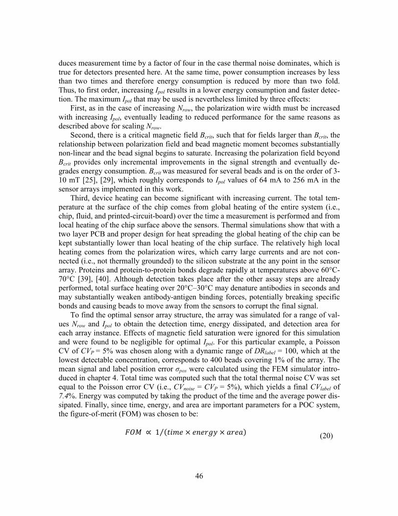
46
duces measurement time by a factor of four in the case thermal noise dominates, which is
true for detectors presented here. At the same time, power consumption increases by less
than two times and therefore energy consumption is reduced by more than two fold.
Thus, to first order, increasing Ipol results in a lower energy consumption and faster detec-
tion. The maximum Ipol that may be used is nevertheless limited by three effects:
First, as in the case of increasing Nrow, the polarization wire width must be increased
with increasing Ipol, eventually leading to reduced performance for the same reasons as
described above for scaling Nrow.
Second, there is a critical magnetic field Bcrit, such that for fields larger than Bcrit, the
relationship between polarization field and bead magnetic moment becomes substantially
non-linear and the bead signal begins to saturate. Increasing the polarization field beyond
Bcrit provides only incremental improvements in the signal strength and eventually de-
grades energy consumption. Bcrit was measured for several beads and is on the order of 3-
10 mT [25], [29], which roughly corresponds to Ipol values of 64 mA to 256 mA in the
sensor arrays implemented in this work.
Third, device heating can become significant with increasing current. The total tem-
perature at the surface of the chip comes from global heating of the entire system (i.e.,
chip, fluid, and printed-circuit-board) over the time a measurement is performed and from
local heating of the chip surface above the sensors. Thermal simulations show that with a
two layer PCB and proper design for heat spreading the global heating of the chip can be
kept substantially lower than local heating of the chip surface. The relatively high local
heating comes from the polarization wires, which carry large currents and are not con-
nected (i.e., not thermally grounded) to the silicon substrate at the any point in the sensor
array. Proteins and protein-to-protein bonds degrade rapidly at temperatures above 60°C-
70°C [39], [40]. Although detection takes place after the other assay steps are already
performed, total surface heating over 20°C–30°C may denature antibodies in seconds and
may substantially weaken antibody-antigen binding forces, potentially breaking specific
bonds and causing beads to move away from the sensors to corrupt the final signal.
To find the optimal sensor array structure, the array was simulated for a range of val-
ues Nrow and Ipol to obtain the detection time, energy dissipated, and detection area for
each array instance. Effects of magnetic field saturation were ignored for this simulation
and were found to be negligible for optimal Ipol. For this particular example, a Poisson
CV of CVP = 5% was chosen along with a dynamic range of DRlabel = 100, which at the
lowest detectable concentration, corresponds to 400 beads covering 1% of the array. The
mean signal and label position error σpos were calculated using the FEM simulator intro-
duced in chapter 4. Total time was computed such that the total thermal noise CV was set
equal to the Poisson error CV (i.e., CVnoise = CVP = 5%), which yields a final CVlabel of
7.4%. Energy was computed by taking the product of the time and the average power dis-
sipated. Finally, since time, energy, and area are important parameters for a POC system,
the figure-of-merit (FOM) was chosen to be:
jk4 ∝ 1 "9l;O Y O�OImg Y `IO`#⁄ (20)
47
Figure 5-2 shows a graph of the FOM (black contours) for different array instances
having different values of Ipol and Nrow. The optimal range lies for Ipol between 128 mA
and 512 mA and Nrow between 16 and 48. At low Ipol and Nrow, the signal is small and the
array does not take advantage of parallelization enough. At high Ipol and Nrow, the wiring
overhead is so large that the average signal drops and position-dependent error increases
beyond the Poisson error, reducing the performance.
Figure 5-2: Contour plots of FOM and maximum surface temperature rise for various
values of polarization current and number of sensors per row.
The optimal currents suggested above are relatively high and cause substantial sur-
face temperature rise. In order to quantitatively characterize the surface heating, thermal
FEM simulations were performed by modeling the sensor row as an infinitely long struc-
ture as was shown previously in Figure 4-8(a). The maximum surface temperature is
overlaid on Figure 5-2 (red contours). In general, the more current is used the more heat
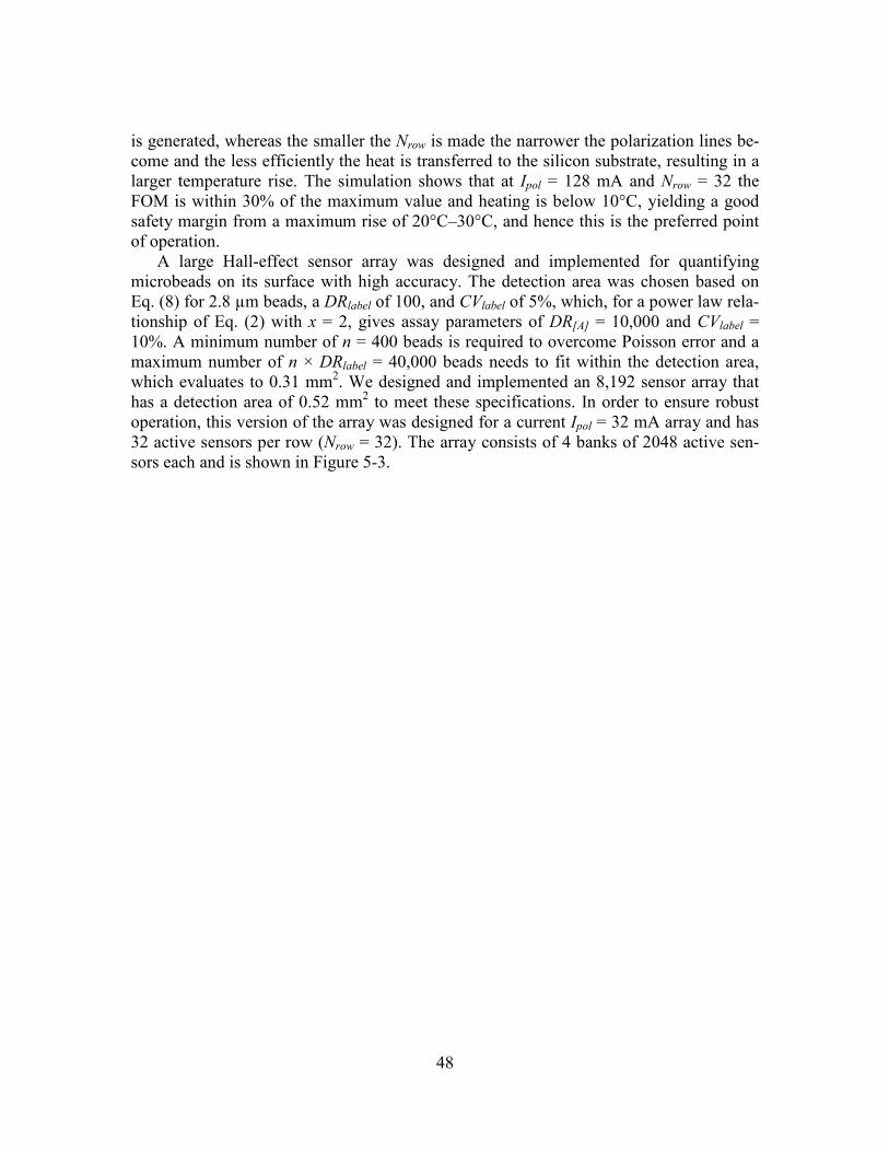
48
is generated, whereas the smaller the Nrow is made the narrower the polarization lines be-
come and the less efficiently the heat is transferred to the silicon substrate, resulting in a
larger temperature rise. The simulation shows that at Ipol = 128 mA and Nrow = 32 the
FOM is within 30% of the maximum value and heating is below 10°C, yielding a good
safety margin from a maximum rise of 20°C–30°C, and hence this is the preferred point
of operation.
A large Hall-effect sensor array was designed and implemented for quantifying
microbeads on its surface with high accuracy. The detection area was chosen based on
Eq. (8) for 2.8 µm beads, a DRlabel of 100, and CVlabel of 5%, which, for a power law rela-
tionship of Eq. (2) with x = 2, gives assay parameters of DR[A] = 10,000 and CVlabel =
10%. A minimum number of n = 400 beads is required to overcome Poisson error and a
maximum number of n × DRlabel = 40,000 beads needs to fit within the detection area,
which evaluates to 0.31 mm2. We designed and implemented an 8,192 sensor array that
has a detection area of 0.52 mm2 to meet these specifications. In order to ensure robust
operation, this version of the array was designed for a current Ipol = 32 mA array and has
32 active sensors per row (Nrow = 32). The array consists of 4 banks of 2048 active sen-
sors each and is shown in Figure 5-3.
49
Figure 5-3: (a) Optical image of the sensor chip containing 4 banks with 2048 active sen-
sors each. (b) One half of a 2048 Hall sensor array bank with M280 beads covering ap-
proximately 2% of the surface.
5.2 Bias and readout circuits
Figure 5-4 shows a high-level diagram of the circuit sub-system [34]. The chip is sub-
divided in two 4,096 sensor sub-arrays, each comprising a polarization current generator,
a timing generation block, and two banks of 2,048 Hall sensors with associated readout
electronics. When a row is selected, digital switches allow polarization current to flow
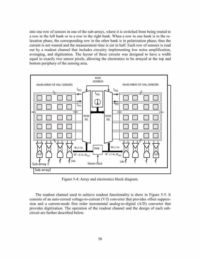
50
into one row of sensors in one of the sub-arrays, where it is switched from being routed to
a row in the left bank or to a row in the right bank. When a row in one bank is in the re-
laxation phase, the corresponding row in the other bank is in polarization phase; thus the
current is not wasted and the measurement time is cut in half. Each row of sensors is read
out by a readout channel that includes circuitry implementing low noise amplification,
averaging, and digitization. The layout of these circuits was designed to have a width
equal to exactly two sensor pixels, allowing the electronics to be arrayed at the top and
bottom periphery of the sensing area.
Figure 5-4: Array and electronics block diagram.
The readout channel used to achieve readout functionality is show in Figure 5-5. It
consists of an auto-zeroed voltage-to-current (V/I) converter that provides offset suppres-
sion and a current-mode first order incremental analog-to-digital (A/D) converter that
provides digitization. The operation of the readout channel and the design of each sub-
circuit are further described below.
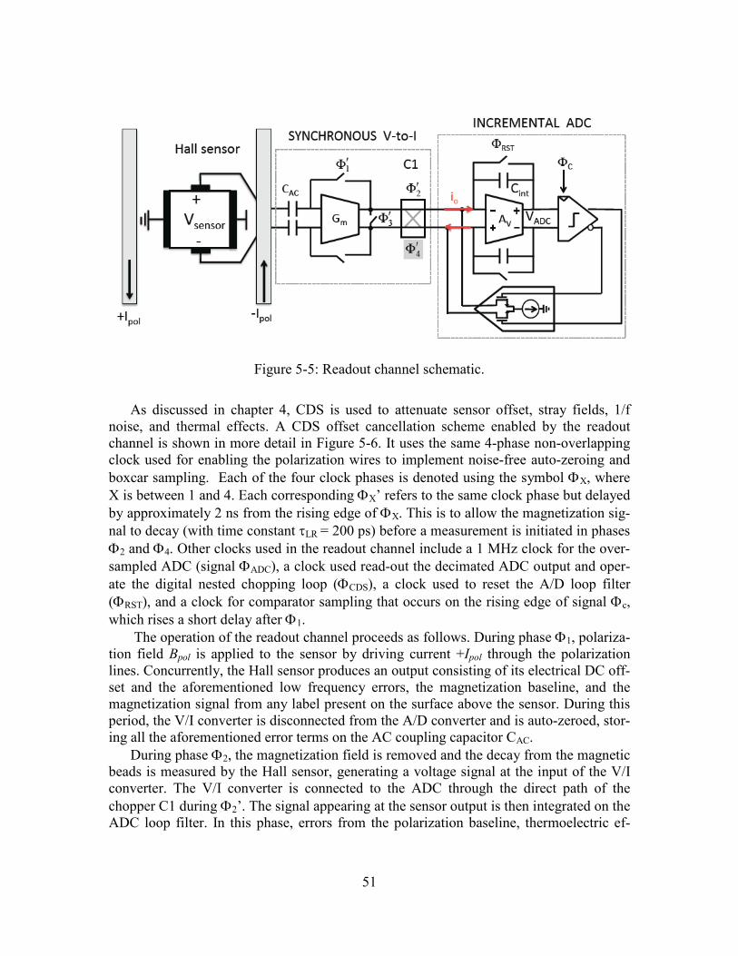
51
Figure 5-5: Readout channel schematic.
As discussed in chapter 4, CDS is used to attenuate sensor offset, stray fields, 1/f
noise, and thermal effects. A CDS offset cancellation scheme enabled by the readout
channel is shown in more detail in Figure 5-6. It uses the same 4-phase non-overlapping
clock used for enabling the polarization wires to implement noise-free auto-zeroing and
boxcar sampling. Each of the four clock phases is denoted using the symbol ΦX, where
X is between 1 and 4. Each corresponding ΦX’ refers to the same clock phase but delayed
by approximately 2 ns from the rising edge of ΦX. This is to allow the magnetization sig-
nal to decay (with time constant τLR = 200 ps) before a measurement is initiated in phases
Φ2 and Φ4. Other clocks used in the readout channel include a 1 MHz clock for the over-
sampled ADC (signal ΦADC), a clock used read-out the decimated ADC output and oper-
ate the digital nested chopping loop (ΦCDS), a clock used to reset the A/D loop filter
(ΦRST), and a clock for comparator sampling that occurs on the rising edge of signal Φc,
which rises a short delay after Φ1.
The operation of the readout channel proceeds as follows. During phase Φ1, polariza-
tion field Bpol is applied to the sensor by driving current +Ipol through the polarization
lines. Concurrently, the Hall sensor produces an output consisting of its electrical DC off-
set and the aforementioned low frequency errors, the magnetization baseline, and the
magnetization signal from any label present on the surface above the sensor. During this
period, the V/I converter is disconnected from the A/D converter and is auto-zeroed, stor-
ing all the aforementioned error terms on the AC coupling capacitor CAC.
During phase Φ2, the magnetization field is removed and the decay from the magnetic
beads is measured by the Hall sensor, generating a voltage signal at the input of the V/I
converter. The V/I converter is connected to the ADC through the direct path of the
chopper C1 during Φ2’. The signal appearing at the sensor output is then integrated on the
ADC loop filter. In this phase, errors from the polarization baseline, thermoelectric ef-
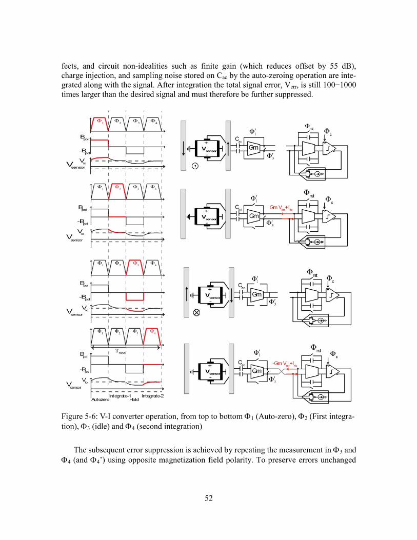
52
fects, and circuit non-idealities such as finite gain (which reduces offset by 55 dB),
charge injection, and sampling noise stored on Cac by the auto-zeroing operation are inte-
grated along with the signal. After integration the total signal error, Verr, is still 100−1000
times larger than the desired signal and must therefore be further suppressed.
Figure 5-6: V-I converter operation, from top to bottom Φ1 (Auto-zero), Φ2 (First integra-
tion), Φ3 (idle) and Φ4 (second integration)
The subsequent error suppression is achieved by repeating the measurement in Φ3 and
Φ4 (and Φ4’) using opposite magnetization field polarity. To preserve errors unchanged
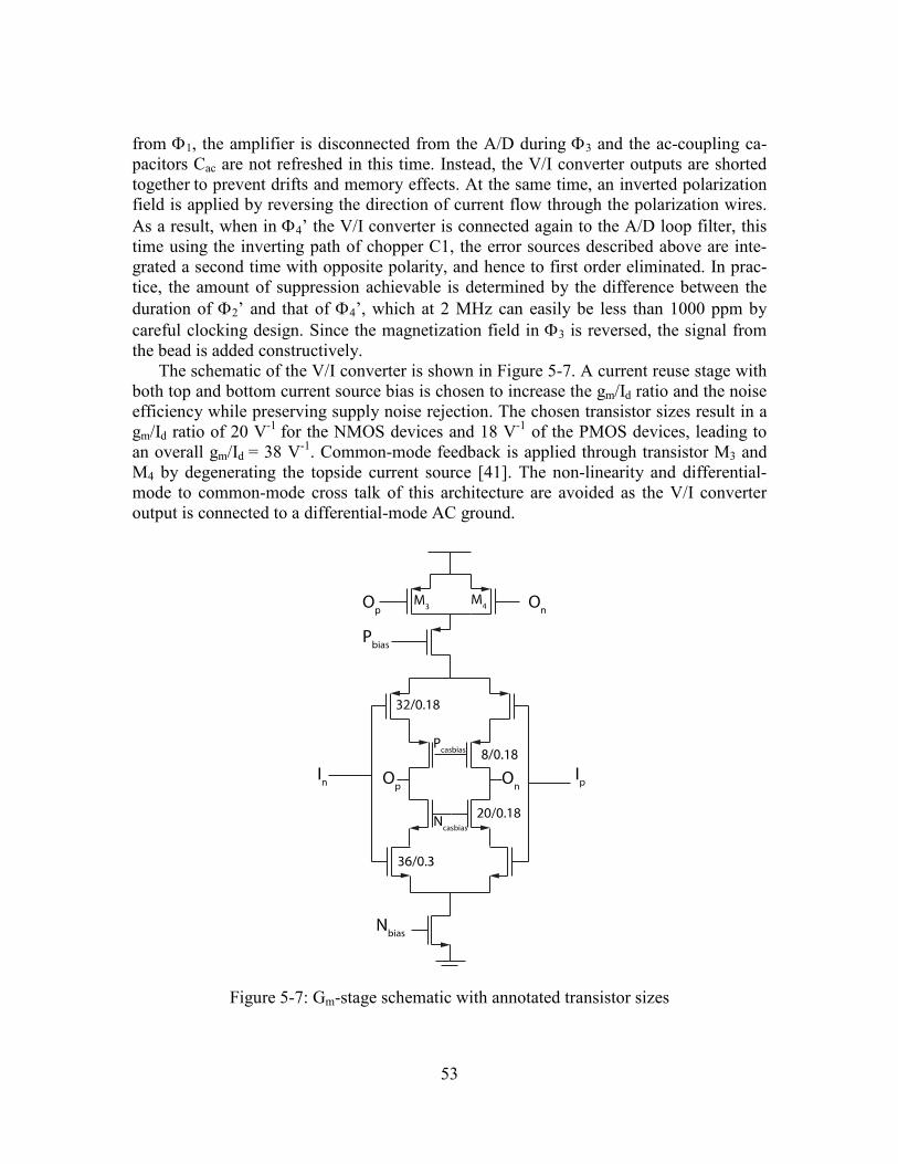
53
from Φ1, the amplifier is disconnected from the A/D during Φ3 and the ac-coupling ca-
pacitors Cac are not refreshed in this time. Instead, the V/I converter outputs are shorted
together to prevent drifts and memory effects. At the same time, an inverted polarization
field is applied by reversing the direction of current flow through the polarization wires.
As a result, when in Φ4’ the V/I converter is connected again to the A/D loop filter, this
time using the inverting path of chopper C1, the error sources described above are inte-
grated a second time with opposite polarity, and hence to first order eliminated. In prac-
tice, the amount of suppression achievable is determined by the difference between the
duration of Φ2’ and that of Φ4’, which at 2 MHz can easily be less than 1000 ppm by
careful clocking design. Since the magnetization field in Φ3 is reversed, the signal from
the bead is added constructively.
The schematic of the V/I converter is shown in Figure 5-7. A current reuse stage with
both top and bottom current source bias is chosen to increase the gm/Id ratio and the noise
efficiency while preserving supply noise rejection. The chosen transistor sizes result in a
gm/Id ratio of 20 V-1
for the NMOS devices and 18 V-1
of the PMOS devices, leading to
an overall gm/Id = 38 V-1
. Common-mode feedback is applied through transistor M3 and
M4 by degenerating the topside current source [41]. The non-linearity and differential-
mode to common-mode cross talk of this architecture are avoided as the V/I converter
output is connected to a differential-mode AC ground.
Figure 5-7: Gm-stage schematic with annotated transistor sizes
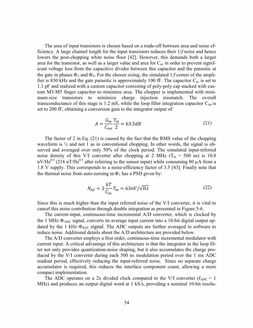
54
The area of input transistors is chosen based on a trade-off between area and noise ef-
ficiency. A large channel length for the input transistors reduces their 1/f noise and hence
lowers the post-chopping white noise floor [42]. However, this demands both a larger
area for the transistor, as well as a larger value and area for Cac in order to prevent signif-
icant voltage loss from the capacitive divider between this capacitor and the parasitic at
the gate in phases Φ2 and Φ4. For the chosen sizing, the simulated 1/f corner of the ampli-
fier is 830 kHz and the gate parasitic is approximately 100 fF. The capacitor Cac is set to
1.1 pF and realized with a custom capacitor consisting of poly-poly cap stacked with cus-
tom M3-M5 finger capacitor to minimize area. The chopper is implemented with mini-
mum-size transistors to minimize charge injection mismatch. The overall
transconductance of this stage is 1.2 mS, while the loop filter integration capacitor Cint is
set to 200 fF, obtaining a conversion gain to the integrator output of:
� � Xn��!5 >n2 � 63.5'< (21)
The factor of 2 in Eq. (21) is caused by the fact that the RMS value of the chopping
waveform is ½ and not 1 as in conventional chopping. In other words, the signal is ob-
served and averaged over only 50% of the clock period. The simulated input-referred
noise density of this V/I converter after chopping at 2 MHz (Tm = 500 ns) is 10.8
nV/Hz0.5
(216 nT/Hz0.5
after referring to the sensor input) while consuming 80 µA from a
1.8 V supply. This corresponds to a noise-efficiency factor of 3.5 [43]. Finally note that
the thermal noise from auto-zeroing in Φ1 has a PSD given by:
r � 2 =>��s >n � 63��/√u] (22)
Since this is much higher than the input referred noise of the V/I converter, it is vital to
cancel this noise contribution through double integration as presented in Figure 5-6.
The current-input, continuous-time incremental A/D converter, which is clocked by
the 1 MHz ΦADC signal, converts its average input current into a 10-bit digital output up-
dated by the 1 kHz ΦRST signal. The ADC outputs are further averaged in software to
reduce noise. Additional details about the A/D architecture are provided below.
The A/D converter employs a first order, continuous-time incremental modulator with
current input. A critical advantage of this architecture is that the integrator in the loop fil-
ter not only provides quantization-noise shaping, but it also accumulates the charge pro-
duced by the V/I converter during each 500 ns modulation period over the 1 ms ADC
readout period, effectively reducing the input-referred noise. Since no separate charge
accumulator is required, this reduces the interface component count, allowing a more
compact implementation.
The ADC operates on a 2x divided clock compared to the V/I converter (fADC = 1
MHz) and produces an output digital word at 1 kS/s, providing a nominal 10-bit resolu-
55
tion. The converter offset, largely determined by the OTA used in the loop filter, can be
as large as 500 µT when referred to the input of the Hall sensor. The ADC also limits the
residual system input-referred flicker noise corner to 1 kHz. This offset and its drift are
suppressed by a nested chopping loop with digital demodulation ([41], [44]) that operates
by exchanging the sign of the magnetization field in Φ1 and Φ3 after each A/D sample is
taken, effectively up-modulating the bead signal with a 1 kS/s square wave. The signal is
demodulated subtracting consecutive A/D output words in the digital domain, removing
residuals 1/f noise and offset, including the contribution of the converter itself. The field
polarity is switched in a silent clock phase (ΦRST), which is also allocated to resetting the
integration capacitor. As a result, to first order no nested chopping transients are ob-
served. Because the offset is suppressed only after digitization, the A/D converter is de-
signed to have a +/-2.5 mT full scale to prevent residual offsets from saturating this block
prior to demodulation. The corresponding quantization noise has an input-referred PSD
of 52 nT/Hz0.5
, well below the V/I converter thermal noise.
Figure 5-8: Circuit Schematics of A/D Converter building blocks: D/A (left) and OTA
(right)
The 1-bit D/A converter is realized with a complementary structure (Figure 5-8),
where both the top and the bottom current sources are switched, leading to a 2x reduction
of thermal noise. The OTA used in the integrator uses a folded-cascode topology with
extra-cascode devices in the input path to provide 75 dB of DC gain and ensure effective
averaging over 1000 samples. Its current consumption is set to 80 µA to provide low ef-
fective input impedance to the V/I converter, thus minimizing signal-dependent charge
injection from chopper C1 without resorting to a two-stage design. Common-mode feed-
back is realized with a switched-capacitor network clocked at 250 kHz. A 14-bit counter
and shift register provides decimation and data output serialization.
56
5.3 Measurement results
5.3.1 Sensor characterization
In addition to the large array having Ipol = 32 mA and Nrow = 32, a high performance
8×8 test array designed for Ipol = 128 mA and Nrow = 32 was implemented. To character-
ize the sensors, each array implementation was tested using 4.5 µm M450® beads as they
can be positioned accurately using a micromanipulator. Table 5-1 lists several parameters
and measurement results obtained for each unit cell. The 128 mA sensors were measured
up to 106 mA due to current routing limitations. Since no degradation of signal due to
bead signal saturation or temperature rise was seen, the results of the 106 mA measure-
ment were extrapolated to Ipol = 128 mA. The 128 mA polarization wires generate 3.2
times larger signals than those generated by the 32 mA polarization wires, mostly be-
cause their current density is further from the sensor/bead than the 32 mA polarization
wires. Sensitivity was simulated across the sensor surface and the simulations were veri-
fied by measuring beads at the top, bottom, and corner of each unit-cell. Despite the sub-
stantially wider polarization lines needed to deliver a 128 mA polarization current, bead
signals are still relatively uniform within the 128 mA sensor unit cell with a σpos = 0.20
for 4.5 µm beads and σpos = 0.47 for 1 µm beads. Even in the worst case of σpos = 0.47, a
5% CVlabel due to Poisson error would be increased by (12 + 0.47
2)1/2
to get a CVlabel of
5.5%, which is a relatively small increase in error.
Sensitivity variations between different sensors in the array were measured to have a
standard deviation of 1.4%, adding negligible signal error. To evaluate the variations in
beads (σsig), signals from several individual 2.8 µm and 4.5 µm beads were measured and
the standard deviation was computed to be σsig = 0.096 for 4.5 µm beads and σsig = 0.31
for 2.8 µm, in both cases much smaller than the Poisson error, indicating that variations
in these labels do not substantially degrade accuracy.
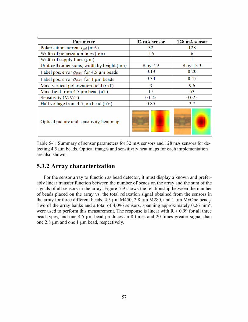
57
Table 5-1: Summary of sensor parameters for 32 mA sensors and 128 mA sensors for de-
tecting 4.5 µm beads. Optical images and sensitivity heat maps for each implementation
are also shown.
5.3.2 Array characterization
For the sensor array to function as bead detector, it must display a known and prefer-
ably linear transfer function between the number of beads on the array and the sum of the
signals of all sensors in the array. Figure 5-9 shows the relationship between the number
of beads placed on the array vs. the total relaxation signal obtained from the sensors in
the array for three different beads, 4.5 µm M450, 2.8 µm M280, and 1 µm MyOne beads.
Two of the array banks and a total of 4,096 sensors, spanning approximately 0.26 mm2,
were used to perform this measurement. The response is linear with R > 0.99 for all three
bead types, and one 4.5 µm bead produces an 8 times and 20 times greater signal than
one 2.8 µm and one 1 µm bead, respectively.
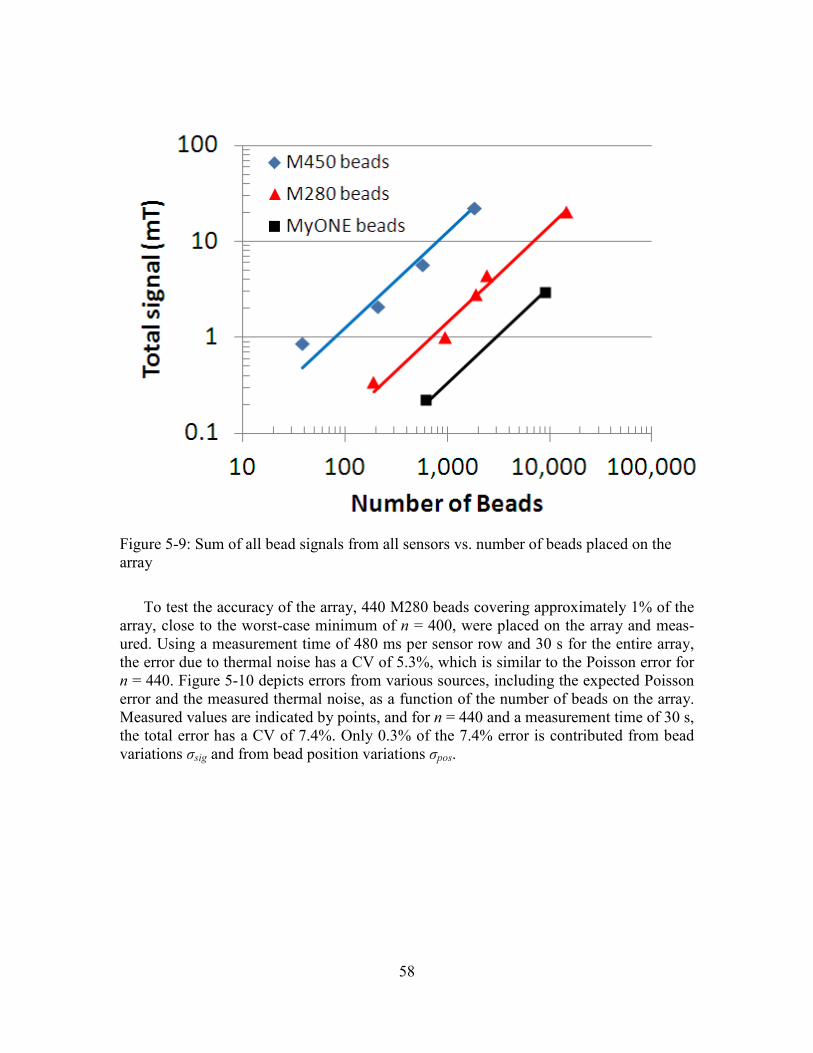
58
Figure 5-9: Sum of all bead signals from all sensors vs. number of beads placed on the
array
To test the accuracy of the array, 440 M280 beads covering approximately 1% of the
array, close to the worst-case minimum of n = 400, were placed on the array and meas-
ured. Using a measurement time of 480 ms per sensor row and 30 s for the entire array,
the error due to thermal noise has a CV of 5.3%, which is similar to the Poisson error for
n = 440. Figure 5-10 depicts errors from various sources, including the expected Poisson
error and the measured thermal noise, as a function of the number of beads on the array.
Measured values are indicated by points, and for n = 440 and a measurement time of 30 s,
the total error has a CV of 7.4%. Only 0.3% of the 7.4% error is contributed from bead
variations σsig and from bead position variations σpos.
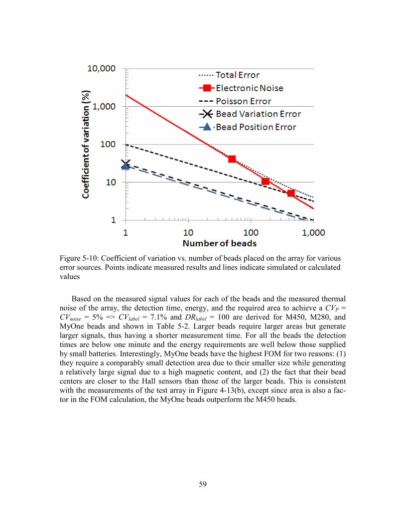
59
Figure 5-10: Coefficient of variation vs. number of beads placed on the array for various
error sources. Points indicate measured results and lines indicate simulated or calculated
values
Based on the measured signal values for each of the beads and the measured thermal
noise of the array, the detection time, energy, and the required area to achieve a CVP =
CVnoise = 5% => CVlabel = 7.1% and DRlabel = 100 are derived for M450, M280, and
MyOne beads and shown in Table 5-2. Larger beads require larger areas but generate
larger signals, thus having a shorter measurement time. For all the beads the detection
times are below one minute and the energy requirements are well below those supplied
by small batteries. Interestingly, MyOne beads have the highest FOM for two reasons: (1)
they require a comparably small detection area due to their smaller size while generating
a relatively large signal due to a high magnetic content, and (2) the fact that their bead
centers are closer to the Hall sensors than those of the larger beads. This is consistent
with the measurements of the test array in Figure 4-13(b), except since area is also a fac-
tor in the FOM calculation, the MyOne beads outperform the M450 beads.
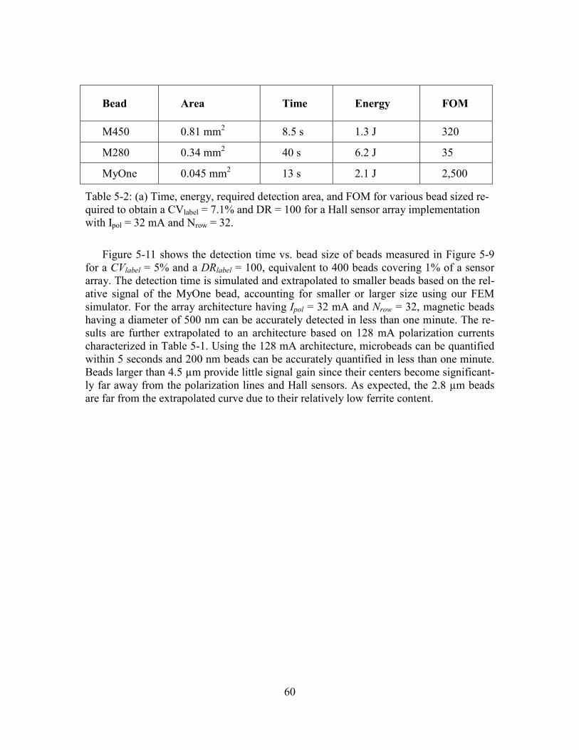
60
Bead Area Time Energy FOM
M450 0.81 mm2 8.5 s 1.3 J 320
M280 0.34 mm2 40 s 6.2 J 35
MyOne 0.045 mm2 13 s 2.1 J 2,500
Table 5-2: (a) Time, energy, required detection area, and FOM for various bead sized re-
quired to obtain a CVlabel = 7.1% and DR = 100 for a Hall sensor array implementation
with Ipol = 32 mA and Nrow = 32.
Figure 5-11 shows the detection time vs. bead size of beads measured in Figure 5-9
for a CVlabel = 5% and a DRlabel = 100, equivalent to 400 beads covering 1% of a sensor
array. The detection time is simulated and extrapolated to smaller beads based on the rel-
ative signal of the MyOne bead, accounting for smaller or larger size using our FEM
simulator. For the array architecture having Ipol = 32 mA and Nrow = 32, magnetic beads
having a diameter of 500 nm can be accurately detected in less than one minute. The re-
sults are further extrapolated to an architecture based on 128 mA polarization currents
characterized in Table 5-1. Using the 128 mA architecture, microbeads can be quantified
within 5 seconds and 200 nm beads can be accurately quantified in less than one minute.
Beads larger than 4.5 µm provide little signal gain since their centers become significant-
ly far away from the polarization lines and Hall sensors. As expected, the 2.8 µm beads
are far from the extrapolated curve due to their relatively low ferrite content.
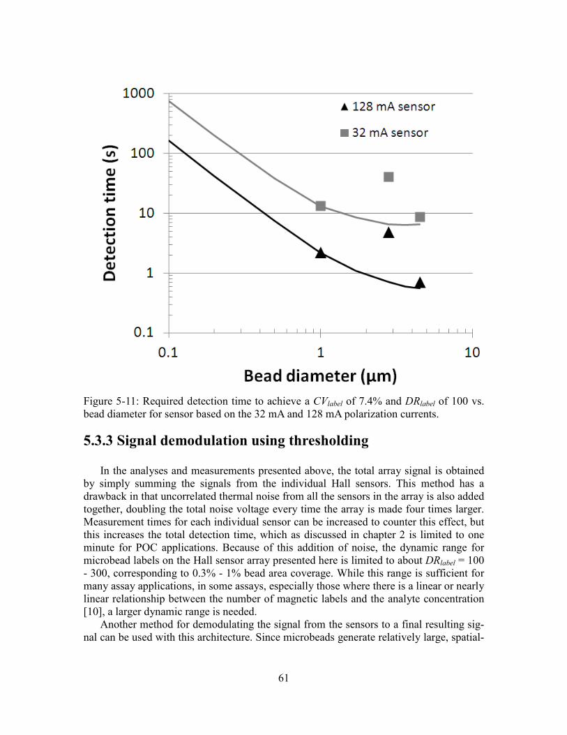
61
Figure 5-11: Required detection time to achieve a CVlabel of 7.4% and DRlabel of 100 vs.
bead diameter for sensor based on the 32 mA and 128 mA polarization currents.
5.3.3 Signal demodulation using thresholding
In the analyses and measurements presented above, the total array signal is obtained
by simply summing the signals from the individual Hall sensors. This method has a
drawback in that uncorrelated thermal noise from all the sensors in the array is also added
together, doubling the total noise voltage every time the array is made four times larger.
Measurement times for each individual sensor can be increased to counter this effect, but
this increases the total detection time, which as discussed in chapter 2 is limited to one
minute for POC applications. Because of this addition of noise, the dynamic range for
microbead labels on the Hall sensor array presented here is limited to about DRlabel = 100
- 300, corresponding to 0.3% - 1% bead area coverage. While this range is sufficient for
many assay applications, in some assays, especially those where there is a linear or nearly
linear relationship between the number of magnetic labels and the analyte concentration
[10], a larger dynamic range is needed.
Another method for demodulating the signal from the sensors to a final resulting sig-
nal can be used with this architecture. Since microbeads generate relatively large, spatial-
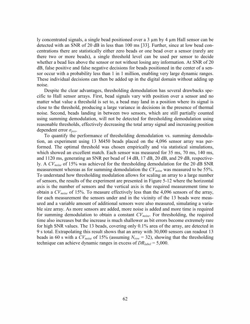
62
ly concentrated signals, a single bead positioned over a 3 µm by 4 µm Hall sensor can be
detected with an SNR of 20 dB in less than 100 ms [33]. Further, since at low bead con-
centrations there are statistically either zero beads or one bead over a sensor (rarely are
there two or more beads), a single threshold level can be used per sensor to decide
whether a bead lies above the sensor or not without losing any information. At SNR of 20
dB, false positive and false negative decisions for beads positioned in the center of a sen-
sor occur with a probability less than 1 in 1 million, enabling very large dynamic ranges.
These individual decisions can then be added up in the digital domain without adding up
noise.
Despite the clear advantages, thresholding demodulation has several drawbacks spe-
cific to Hall sensor arrays. First, bead signals vary with position over a sensor and no
matter what value a threshold is set to, a bead may land in a position where its signal is
close to the threshold, producing a large variance in decisions in the presence of thermal
noise. Second, beads landing in between two sensors, which are still partially counted
using summing demodulation, will not be detected for thresholding demodulation using
reasonable thresholds, effectively decreasing the total array signal and increasing position
dependent error σpos.
To quantify the performance of thresholding demodulation vs. summing demodula-
tion, an experiment using 13 M450 beads placed on the 4,096 sensor array was per-
formed. The optimal threshold was chosen empirically and via statistical simulations,
which showed an excellent match. Each sensor was measured for 35 ms, 70 ms, 140 ms,
and 1120 ms, generating an SNR per bead of 14 dB, 17 dB, 20 dB, and 29 dB, respective-
ly. A CVnoise of 15% was achieved for the thresholding demodulation for the 20 dB SNR
measurement whereas as for summing demodulation the CVnoise was measured to be 55%.
To understand how thresholding modulation allows for scaling an array to a large number
of sensors, the results of the experiment are presented in Figure 5-12 where the horizontal
axis is the number of sensors and the vertical axis is the required measurement time to
obtain a CVnoise of 15%. To measure effectively less than the 4,096 sensors of the array,
for each measurement the sensors under and in the vicinity of the 13 beads were meas-
ured and a variable amount of additional sensors were also measured, simulating a varia-
ble size array. As more sensors are added, more noise is added and more time is required
for summing demodulation to obtain a constant CVnoise. For thresholding, the required
time also increases but the increase is much shallower as bit errors become extremely rare
for high SNR values. The 13 beads, covering only 0.1% area of the array, are detected in
9 s total. Extrapolating this result shows that an array with 30,000 sensors can readout 13
beads in 60 s with a CVnoise of 15% (assuming Nrow = 32), showing that the thresholding
technique can achieve dynamic ranges in excess of DRlabel = 5,000.
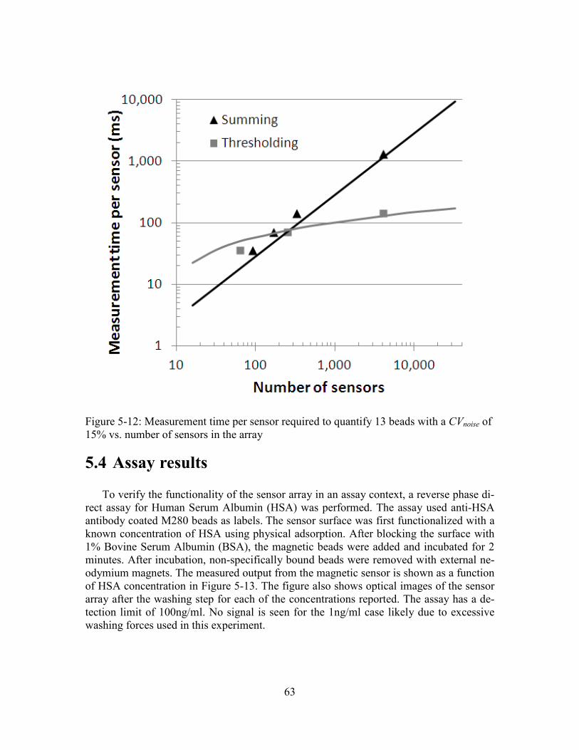
63
Figure 5-12: Measurement time per sensor required to quantify 13 beads with a CVnoise of
15% vs. number of sensors in the array
5.4 Assay results
To verify the functionality of the sensor array in an assay context, a reverse phase di-
rect assay for Human Serum Albumin (HSA) was performed. The assay used anti-HSA
antibody coated M280 beads as labels. The sensor surface was first functionalized with a
known concentration of HSA using physical adsorption. After blocking the surface with
1% Bovine Serum Albumin (BSA), the magnetic beads were added and incubated for 2
minutes. After incubation, non-specifically bound beads were removed with external ne-
odymium magnets. The measured output from the magnetic sensor is shown as a function
of HSA concentration in Figure 5-13. The figure also shows optical images of the sensor
array after the washing step for each of the concentrations reported. The assay has a de-
tection limit of 100ng/ml. No signal is seen for the 1ng/ml case likely due to excessive
washing forces used in this experiment.
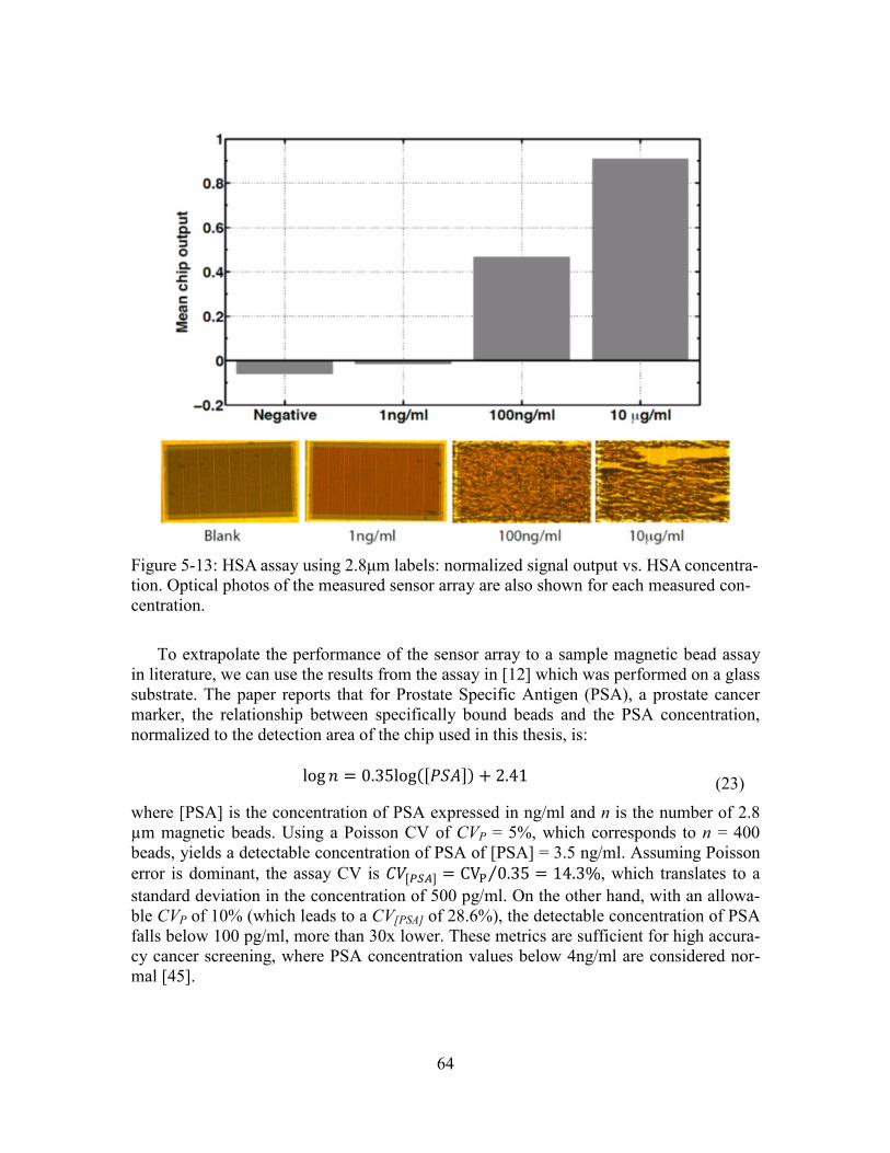
64
Figure 5-13: HSA assay using 2.8µm labels: normalized signal output vs. HSA concentra-
tion. Optical photos of the measured sensor array are also shown for each measured con-
centration.
To extrapolate the performance of the sensor array to a sample magnetic bead assay
in literature, we can use the results from the assay in [12] which was performed on a glass
substrate. The paper reports that for Prostate Specific Antigen (PSA), a prostate cancer
marker, the relationship between specifically bound beads and the PSA concentration,
normalized to the detection area of the chip used in this thesis, is:
log � � 0.35log"�z{�# � 2.41 (23)
where [PSA] is the concentration of PSA expressed in ng/ml and n is the number of 2.8
µm magnetic beads. Using a Poisson CV of CVP = 5%, which corresponds to n = 400
beads, yields a detectable concentration of PSA of [PSA] = 3.5 ng/ml. Assuming Poisson
error is dominant, the assay CV is ����| � CV� 0.35⁄ � 14.3%, which translates to a
standard deviation in the concentration of 500 pg/ml. On the other hand, with an allowa-
ble CVP of 10% (which leads to a CV[PSA] of 28.6%), the detectable concentration of PSA
falls below 100 pg/ml, more than 30x lower. These metrics are sufficient for high accura-
cy cancer screening, where PSA concentration values below 4ng/ml are considered nor-
mal [45].
65
6 Conclusion
Magnetic beads are excellent candidates for labels in biological assays performed on
integrated platforms. In this work we have demonstrated that magnetic beads on the order
of 1 µm in diameter can be quantified with accuracies sufficient for biological assays in
detection areas small enough to fit on CMOS chips and with a detection time and energy
suitable for POC settings. Magnetic bead detectors based on n-well Hall sensors and po-
larization wires were designed in a 0.18 µm CMOS process and display a good combina-
tion of sensitivity and robustness. Relaxation detection and one-point calibration tech-
niques were applied to further increase the accuracy of bead detection. The individual
sensors were organized into a 4,096 sensor, 0.26 mm2 array that can quantify a 1% sur-
face coverage of magnetic microbeads with a worst case CV of 7.4% within one minute
while dissipating less than 10 J of energy, less than 1/2000 of the energy stored on a typi-
cal smartphone battery. Utilizing thresholding demodulation, a feature of this implemen-
tation due to the inherent array-based design, beads covering only 0.1% of the sensor ar-
ray can be detected in just a few seconds with high accuracy. The microchip was tested in
a biological setting and is capable of detecting beads in biological conditions with protein
concentrations down to the 100pg/ml levels. To conclude, robust and compact detection
platforms based on CMOS Hall-effect sensors and magnetic microbead labels are suitable
for high accuracy point-of-care assays.
66
7 References
[1] M. Urdea, L. A. Penny, S. S. Olmsted, M. Y. Giovanni, P. Kaspar, A. Shepherd, P.
Wilson, C. A. Dahl, S. Buchsbaum, G. Moeller, and D. C. H. Burgess, “Require-
ments for high impact diagnostics in the developing world,” Nature, vol. 444, pp. 73–
79, Nov. 2006.
[2] F. B. Myers and L. P. Lee, “Innovations in optical microfluidic technologies for
point-of-care diagnostics,” Lab on a Chip, vol. 8, no. 12, p. 2015, 2008.
[3] H. Tomaso, P. Thullier, E. Seibold, V. Guglielmo, A. Buckendahl, L. Rahalison, H.
Neubauer, H. C. Scholz, and W. D. Splettstoesser, “Comparison of Hand-Held Test
Kits, Immunofluorescence Microscopy, Enzyme-Linked Immunosorbent Assay, and
Flow Cytometric Analysis for Rapid Presumptive Identification of Yersinia pestis,” J
Clin Microbiol, vol. 45, no. 10, pp. 3404–3407, Oct. 2007.
[4] “Rapid Troponin I Test Strip.” Bio-Quant, Inc., Jun-2005.
[5] C. Martín-Hernández, M. Muñoz, C. Daury, H. Weymuth, A. E. M. Kemmers-
Voncken, V. Corbatón, T. Toribio, and M. G. E. G. Bremer,
“Immunochromatographic lateral-flow test strip for the rapid detection of added bo-
vine rennet whey in milk and milk powder,” International Dairy Journal, vol. 19, no.
4, pp. 205–208, Apr. 2009.
[6] F. Oberpenning, S. Hetzel, C. Weining, B. Brandt, G. De Angelis, A. Heinecke, M.
Lein, P. Fornara, H.-P. Schmid, L. Hertle, and A. Semjonow, “Semi-Quantitative
Immunochromatographic Test for Prostate Specific Antigen in Whole Blood: Tossing
the Coin to Predict Prostate Cancer?,” European Urology, vol. 43, no. 5, pp. 478–
484, May 2003.
[7] J. A. Alhashemi, “Diagnostic accuracy of a bedside qualitative
immunochromatographic test for acute myocardial infarction,” The American Journal
of Emergency Medicine, vol. 24, no. 2, pp. 149–155, Mar. 2006.
[8] H. Counihan, S. A. Harvey, M. Sekeseke-Chinyama, B. Hamainza, R. Banda, T.
Malambo, F. Masaninga, and D. Bell, “Community Health Workers Use Malaria
Rapid Diagnostic Tests (RDTs) Safely and Accurately: Results of a Longitudinal
Study in Zambia,” Am J Trop Med Hyg, vol. 87, no. 1, pp. 57–63, Jul. 2012.
[9] O. Florescu, K. Wang, P. Au, J. Tang, E. Harris, P. R. Beatty, and B. E. Boser, “On-
chip magnetic separation of superparamagnetic beads for integrated molecular analy-
sis,” Journal of Applied Physics, vol. 107, no. 5, pp. 054702–054702–10, Mar. 2010.
[10] D. M. Bruls, T. H. Evers, J. A. H. Kahlman, P. J. W. van Lankvelt, M. Ovsyanko,
E. G. M. Pelssers, J. J. H. B. Schleipen, F. K. de Theije, C. A. Verschuren, T. van der
Wijk, J. B. A. van Zon, W. U. Dittmer, A. H. J. Immink, J. H. Nieuwenhuis, and M.
W. J. Prins, “Rapid integrated biosensor for multiplexed immunoassays based on ac-
tuated magnetic nanoparticles,” Lab on a Chip, vol. 9, no. 24, p. 3504, 2009.
[11] T. Aytur, P. R. Beatty, B. Boser, M. Anwar, and T. Ishikawa, “An immunoassay
platform based on cmos hall sensors,” in Solid State Sensor, Actuator and Microsys-
tems Workshop, 2002, pp. 126–129.
67
[12] J. Kim, E. C. Jensen, M. Megens, B. Boser, and R. A. Mathies, “Integrated mi-
crofluidic bioprocessor for solid phase capture immunoassays,” Lab Chip, vol. 11,
no. 18, pp. 3106–3112, Sep. 2011.
[13] K. Skucha, P. Liu, M. Megens, J. Kim, and B. Boser, “A compact Hall-effect
sensor array for the detection and imaging of single magnetic beads in biomedical as-
says,” 2011, pp. 1833–1836.
[14] M. B. Pepys and G. M. Hirschfield, “C-reactive protein: a critical update,” Jour-
nal of Clinical Investigation, vol. 111, no. 12, pp. 1805–1812, Jun. 2003.
[15] D. E. Bruns and J. C. Boyd, “Few Point-of-Care Hemoglobin A1c Assay Meth-
ods Meet Clinical Needs,” Clinical Chemistry, vol. 56, no. 1, pp. 4–6, Jan. 2010.
[16] W. de Jager and G. T. Rijkers, “Solid-phase and bead-based cytokine immunoas-
say: a comparison,” Methods, vol. 38, no. 4, pp. 294–303, Apr. 2006.
[17] R. S. Gaster, D. A. Hall, C. H. Nielsen, S. J. Osterfeld, H. Yu, K. E. Mach, R. J.
Wilson, B. Murmann, J. C. Liao, S. S. Gambhir, and S. X. Wang, “Matrix-insensitive
protein assays push the limits of biosensors in medicine,” Nature Medicine, vol. 15,
no. 11, pp. 1327–1332, 2009.
[18] T. Aytur, J. Foley, M. Anwar, B. Boser, E. Harris, and P. R. Beatty, “A novel
magnetic bead bioassay platform using a microchip-based sensor for infectious dis-
ease diagnosis,” J. Immunol. Methods, vol. 314, no. 1–2, pp. 21–29, Jul. 2006.
[19] M. Z. Atassi and C. J. V. Oss, Molecular Immunology: A Textbook. CRC Press,
1984.
[20] A. Hassibi, S. Zahedi, R. Navid, R. W. Dutton, and T. H. Lee, “Biological shot-
noise and quantum-limited signal-to-noise ratio in affinity-based biosensors,” Journal
of Applied Physics, vol. 97, no. 8, pp. 084701–084701–10, Apr. 2005.
[21] S. P. Mulvaney, H. M. Mattoussi, and L. J. Whitman, “Incorporating fluorescent
dyes and quantum dots into magnetic microbeads for immunoassays,”
BioTechniques, vol. 36, no. 4, pp. 602–606, 608–609, Apr. 2004.
[22] M. Hall, I. Kazakova, and Y. M. Yao, “High sensitivity immunoassays using par-
ticulate fluorescent labels,” Anal. Biochem., vol. 272, no. 2, pp. 165–170, Aug. 1999.
[23] X.-W. Zhao, Z.-B. Liu, H. Yang, K. Nagai, Y.-H. Zhao, and Z.-Z. Gu, “Uniform-
ly Colorized Beads for Multiplex Immunoassay,” Chem. Mater., vol. 18, no. 9, pp.
2443–2449, 2006.
[24] B.-I. Haukanes and C. Kvam, “Application of Magnetic Beads in Bioassays,”
Nature Biotechnology, vol. 11, no. 1, pp. 60–63, 1993.
[25] D. R. Baselt, G. U. Lee, M. Natesan, S. W. Metzger, P. E. Sheehan, and R. J.
Colton, “A biosensor based on magnetoresistance technology,” Biosensors and Bioe-
lectronics, vol. 13, no. 7–8, pp. 731–739, Oct. 1998.
[26] J. C. Rife, M. M. Miller, P. E. Sheehan, C. R. Tamanaha, M. Tondra, and L. J.
Whitman, “Design and performance of GMR sensors for the detection of magnetic
microbeads in biosensors,” Sensors and Actuators A: Physical, vol. 107, no. 3, pp.
209–218, Nov. 2003.
[27] H. Wang, Y. Chen, A. Hassibi, A. Scherer, and A. Hajimiri, “A frequency-shift
CMOS magnetic biosensor array with single-bead sensitivity and no external mag-
68
net,” in Solid-State Circuits Conference - Digest of Technical Papers, 2009. ISSCC
2009. IEEE International, 2009, pp. 438 –439,439a.
[28] P. Liu, “A CMOS Magnetic Sensor Chip for Biomedical Applications,” EECS
Department, University of California, Berkeley, 2012.
[29] G. Fonnum, C. Johansson, A. Molteberg, S. Mørup, and E. Aksnes, “Characteri-
sation of Dynabeads® by magnetization measurements and Mössbauer spectrosco-
py,” Journal of Magnetism and Magnetic Materials, vol. 293, no. 1, pp. 41–47, May
2005.
[30] P.-A. Besse, G. Boero, M. Demierre, V. Pott, and R. Popovic, “Detection of a
single magnetic microbead using a miniaturized silicon Hall sensor,” Applied Physics
Letters, vol. 80, no. 22, pp. 4199–4201, Jun. 2002.
[31] O. Florescu, M. Mattmann, and B. Boser, “Fully integrated detection of single
magnetic beads in complementary metal-oxide-semiconductor,” Journal of Applied
Physics, vol. 103, no. 4, pp. 046101–046101–3, Feb. 2008.
[32] P. Liu, K. Skucha, M. Megens, and B. Boser, “A CMOS Hall-Effect Sensor for
the Characterization and Detection of Magnetic Nanoparticles for Biomedical Appli-
cations,” Magnetics, IEEE Transactions on, vol. 47, no. 10, pp. 3449 –3451, Oct.
2011.
[33] P. P. Liu, K. Skucha, Y. Duan, M. Megens, J. Kim, I. I. Izyumin, S. Gambini,
and B. Boser, “Magnetic Relaxation Detector for Microbead Labels,” Solid-State
Circuits, IEEE Journal of, vol. 47, no. 4, pp. 1056 –1064, Apr. 2012.
[34] S. Gambini, K. Skucha, P. Liu, J. Kim, R. Krigel, R. Mathies, and B. Boser, “A
CMOS 10K pixel baseline-free magnetic bead detector with column parallel readout
for miniaturized immunoassays,” Solid-State Circuits, IEEE Journal of, vol. In press.
[35] K. Skucha, S. Gambini, P. P. Liu, M. Megens, J. Kim, and B. Boser, “Design
considerations for CMOS-integrated Hall-effect magnetic bead detectors for biosen-
sor applications,” Microelectromechanical Systems, IEEE/ASME Journal of, no.
Submitted, Jun. 2012.
[36] R. S. Gaster, D. A. Hall, and S. X. Wang, “nanoLAB: An ultraportable, handheld
diagnostic laboratory for global health,” Lab Chip, vol. 11, no. 5, pp. 950–956, Mar.
2011.
[37] R. S. Popovic, Hall Effect Devices, Second Edition, 2nd ed. Taylor & Francis,
2012.
[38] N. Mathieu, P. Giordano, and A. Chovet, “Si MAGFETs optimized for sensitivity
and noise properties,” Sensors and Actuators A: Physical, vol. 32, no. 1–3, pp. 656–
660, Apr. 1992.
[39] A. W. Vermeer and W. Norde, “The thermal stability of immunoglobulin: un-
folding and aggregation of a multi-domain protein,” Biophys. J., vol. 78, no. 1, pp.
394–404, Jan. 2000.
[40] F. Schwesinger, R. Ros, T. Strunz, D. Anselmetti, H.-J. Güntherodt, A. Honeg-
ger, L. Jermutus, L. Tiefenauer, and A. Plückthun, “Unbinding Forces of Single An-
tibody-Antigen Complexes Correlate with Their Thermal Dissociation Rates,” PNAS,
vol. 97, no. 18, pp. 9972–9977, Aug. 2000.
69
[41] J. C. van der Meer, F. R. Riedijk, E. van Kampen, K. A. A. Makinwa, and J. H.
Huijsing, “A fully integrated CMOS Hall sensor with a 3.65 mu;T 3 sigma; offset for
compass applications,” in Solid-State Circuits Conference, 2005. Digest of Technical
Papers. ISSCC. 2005 IEEE International, 2005, pp. 246 –247 Vol. 1.
[42] C. C. Enz and G. C. Temes, “Circuit techniques for reducing the effects of op-
amp imperfections: autozeroing, correlated double sampling, and chopper stabiliza-
tion,” Proceedings of the IEEE, vol. 84, no. 11, pp. 1584 –1614, Nov. 1996.
[43] M. S. J. Steyaert and W. M. C. Sansen, “A micropower low-noise monolithic in-
strumentation amplifier for medical purposes,” IEEE Journal of Solid-State Circuits,
vol. 22, no. 6, pp. 1163 – 1168, Dec. 1987.
[44] A. Bakker, K. Thiele, and J. H. Huijsing, “A CMOS nested-chopper instrumenta-
tion amplifier with 100-nV offset,” IEEE Journal of Solid-State Circuits, vol. 35, no.
12, pp. 1877 –1883, Dec. 2000.
[45] W. J. Catalona, D. S. Smith, and D. K. Ornstein, “Prostate cancer detection in
men with serum PSA concentrations of 2.6 to 4.0 ng/mL and benign prostate exami-
nation. Enhancement of specificity with free PSA measurements,” JAMA, vol. 277,
no. 18, pp. 1452–1455, May 1997.