design, fabrication, and characterization of a short range
TRANSCRIPT

Design, Fabrication, and Characterization of a Short Range, Multi Band Frequency Jammer
by
George Douglas Hughes
A thesis submitted to the Graduate Faculty of Auburn University
in partial fulfillment of the requirements for the Degree of
Master of Science
Auburn, Alabama May 10, 2015
Approved by
Michael C. Hamilton, Chair, Assistant Professor of Electrical and Computer Engineering
Robert Dean, Associate Professor of Electrical and Computer Engineering Stuart Wentworth, Associate Professor of Electrical and Computer Engineering

ii
Abstract
The purpose of this thesis is to show how frequency jamming against wireless communication
systems can be achieved in a modular form so multiple bands can be targeted depending on the need. In
this thesis, the basic fundamentals of frequency jamming will be discussed with an emphasis on time-
division multiple access and code-division multiple access communication systems. The electronic design
will be examined to determine what techniques are needed to create the jamming signal along with the
characterization of the jamming signal to show which techniques are best to optimize the output.
iii
Acknowledgements
The author would like to thank Dr. Michael C. Hamilton for serving as his advisor and for the
assistance throughout this work and graduate studies. Dr. Robert Dean and Dr. Stuart Wentworth are
also thanked for their review and commentary on this work.
The author would also like to thank Thomas P. Stegeman, Will Abell, Justin Moses, and Brett
Byer for their assistance in aspects of this work.
A personal appreciation goes to Richard and Daphne Hughes for their support through the
author’s academic career.

iv
Table of Contents
Abstract ......................................................................................................................................................... ii
Acknowledgements ...................................................................................................................................... iii
List of Tables ................................................................................................................................................ vi
List of Figures .............................................................................................................................................. vii
1 Intorduction ........................................................................................................................................... 1
2 Background ............................................................................................................................................ 2
2.1 Overview of GSM Standard .............................................................................................................. 2
2.2 Overview of CDMA Standard ............................................................................................................ 3
2.3 Theory of Frequency Jamming of Wireless Communication ............................................................ 4
2.4 A Brief Understanding of VCOs ........................................................................................................ 7
2.5 Grounded Coplanar Waveguide ....................................................................................................... 8
2.6 Capacitor Charging and Discharging Characteristics ........................................................................ 9
3 Circuit and Board Design ..................................................................................................................... 14
3.1 Overview of Frequency Jammer Design ......................................................................................... 15
3.2 RF Circuitry ..................................................................................................................................... 15
3.2.1 VCO Tuning Signal Using Only Noise ...................................................................................... 16
3.2.2 VCO Tuning Signal Using a Triangular Wave .......................................................................... 17
3.2.3 Amplifier circuit design........................................................................................................... 20
3.2.4 Power Combiner Circuit ......................................................................................................... 21
3.3 DC Circuitry ..................................................................................................................................... 22
3.4 Board Design .................................................................................................................................. 24

v
3.4.1 KiCad Overview ...................................................................................................................... 25
3.4.2 Multiple Boards for Testing .................................................................................................... 25
4 Measurements of Jamming Signal....................................................................................................... 29
4.1 Response to a Single Tone .............................................................................................................. 29
4.2 Increasing Bandwidth using Noise ................................................................................................. 33
4.3 Jamming Using Noise Added to a Triangular Wave ....................................................................... 35
4.3.1 Frequency of the Triangular Wave ......................................................................................... 36
4.3.2 Bandwidth of Noise Added to the Triangular Wave .............................................................. 53
4.3.3 Frequency Range that the Triangular Wave Covers ............................................................... 57
4.4 Transmission of the Jamming Signal .............................................................................................. 61
5 Conclusions and Future Work ............................................................................................................. 64
5.1 Conclusions ..................................................................................................................................... 64
5.2 Future Work ................................................................................................................................... 66
References .................................................................................................................................................. 68

vi
List of Tables
4.1 R1, R2, and C1 values that control the frequencies of the 555 timers used to test the
ROS-1000PV VCO .......................................................................................................................... 36
4.2 R1, R2, and C1 values that control the frequencies of the 555 timers used to test the
ROS-892-119+ VCO ....................................................................................................................... 43

vii
List of Figures
2.1 Board layout of a grounded coplanar waveguide transmission line .............................................. 9
2.2 RC circuit for capacitor charging equation ...................................................................................... 9
2.3 Charging of a capacitor in a RC circuit ........................................................................................... 10
2.4 Source free RC circuit for capacitor discharging ........................................................................... 11
2.5 Source free RC circuit for capacitor discharging ........................................................................... 12
2.6 RC circuit used in this project to change the pulse to a triangular wave ..................................... 13
3.1 Simple block diagram of a single band frequency jammer ........................................................... 15
3.2 Schematic of the noise generator, DC bias, and operational amplifier circuit ............................. 17
3.3 Schematic of 555 timer in astable mode with RC network for creation of triangular wave ........ 19
3.4 Schematic to create the tuning wave using a triangular wave ..................................................... 20
3.5 Schematic of PMA-545G1+ amplifier circuit ................................................................................. 21
3.6 Power combiner and filter schematic ........................................................................................... 22
3.7 Schematic of 12V boost circuitry .................................................................................................. 23
3.8 5V boost circuitry .......................................................................................................................... 24
3.9 (a) VCO and tuning circuity board, (b) amplifier board, and (c) power combiner board ........ 27-28
4.1 Single tone frequencies of the CDMA and GSM VCOs .................................................................. 30
4.2 Amplification of single tones by PMA-545G1+ .............................................................................. 32
4.3 VCO outputs from two different bandwidths of noise ................................................................. 33
4.4 Amplification of full bandwidth of noise using only noise in the tuning signal ............................ 34

viii
4.5 VCO and amplifier output spectrums of the (a) 2 MHz, (b) 200 kHz, (c) 20 kHz, and (d) 2 kHz
triangular wave tuning signals with no noise .......................................................................... 37-38
4.6 VCO and amplifier output spectrums of the (a) 2 MHz, (b) 200 kHz, (c) 20 kHz, and (d) 2 kHz
triangular wave tuning signals with 10 MHz of noise added ................................................... 40-41
4.7 VCO and amplifier output spectrums of the (a) 500 kHz, (b) 300 kHz, (c) 100 kHz, and (d) 50 kHz
triangular wave tuning signals with no noise added ............................................................... 44-45
4.8 VCO and amplifier output spectrums of the (a) 500 kHz, (b) 300 kHz, (c) 100 kHz, and (d) 50 kHz
triangular wave tuning signals with 10 MHz of noise added ................................................... 46-47
4.9 Mean and standard deviation of power levels for jamming signals with no noise added to the
triangular wave ............................................................................................................................. 50
4.10 Mean and standard deviation of power levels for jamming signals with 10 MHz noise added to
the triangular wave ....................................................................................................................... 51
4.11 CDMA jamming signal with 10, 5, and 2.5 MHz of noise swept across frequency range ............. 54
4.12 GSM jamming signal with 10, 5, and 2.5 MHz of noise swept across frequency range ............... 55
4.13 Mean and standard deviation of the power levels for the 2.5, 5, and 10 MHz of noise swept
across the frequency range ........................................................................................................... 56
4.14 ROS-892-119+ VCO and amplifier jamming signals with 25, 50 and 100 MHz frequency spans .. 58
4.15 ROS-1000PV VCO and amplifier jamming signals with 25, 50 and 100 MHz frequency spans .... 59
4.16 Mean and standard deviation of power levels of the jamming signals that span 25, 50, and 100
MHz ............................................................................................................................................... 60
4.17 CDMA and GSM jamming signal output from the power combiner ............................................. 62

1
Chapter 1
Introduction
Frequency jamming is the act of intentionally disrupting the data transfer of wireless
communication by means of an interfering signal [1, p. 177] [2, p. 291]. In the United States, the use of
frequency jammers designed to intentionally interfere with radio communications is illegal. Section
2.803 of The Commission’s Rules “prohibits the manufacture, importation, marketing, sale or operation
of these devices within the United States” although Section 2.807 “provides for certain limited
exceptions, such as the sale to U.S. government users” [3]. This work will examine the functionality of a
modular frequency jammer that could be used by authorized personnel to prevent a harmful act by
means of wireless communications, such as the remote detonation of an explosive device. This work will
examine the creation of a jamming signal that is intended to have a very short effective area so that the
intended device is affected while not disrupting the communications of unintended devices. In this
work, it is assumed that the detonation signal is not known other than the communication standard that
it is being transmitted over. For this reason, the jamming signal will be designed for a specific standard
which can be duplicated for additional frequency ranges that are determined a likely source of the
detonating signal. For the purposes of this work, code division multiple access (CDMA) and time division
multiple access (TDMA) will be examined in the CDMA and GSM (Global System for Mobile
Communication) cellular technologies that cellular phones currently use. Even though this paper will
only look at these particular schemes, other frequency standards may be jammed in the same fashion as
CDMA and GSM although certain adjustments might have to be made which will be covered in the
following chapters.
2
Chapter 2
Background
In this chapter, the background information will be discussed about the theory and practices
used in the rest of the thesis. The background information includes the theory of frequency jamming
and the pertinent information of GSM and CDMA communication standards as it applies to the jamming
signal. The basic understanding of certain parts and board design will also be discussed as it pertains to
how they are applied to this design.
2.1 Overview of GSM Standard
One of the wireless standards that the jammer in this thesis will be designed for is the Global
System for Mobile Communication (GSM). GSM was initially developed in Europe, but became “the most
widely-used cellular standard in the world”. The GSM standard, which is a TDMA system with GMSK
(Gaussian Minimum Shift Keying) modulation, can support both data and voice transmission and
operates in different bands called GSM900, GSM1800 (also called DCS 1800), and GSM1900 (also called
PCS 1900) [4, p. 132]. TDMA is a multiple-access network where the same band is available to multiple
users at different times so the cellular carrier can have multiple people using the same frequency [4, p.
125]. The GSM standard allows for eight time-multiplexed users on a 200 kHz wide channel with a data
rate per user of 271kb/s. To make sure the transmitter and receiver paths do not operate
simultaneously, the transmitter and receiver time slots are offset by about 1.73 ms. This GSM standard
was extended to accommodate higher data rates (384 kb/s per user) to “enhanced Data Rates for GSM
Evolution” (EDGE). EDGE also differs by the use of 8-PSK (Phase Shift Keying) modulation instead of

3
GMSK. An output power of +33 dBm must be provided by the transmitter in the 900 MHz band and
+30dBm in the 1.8 GHz band. [4, p. 132 and 136]. The frame duration, or the time that the receiver
receives the data in its time slot, for GSM EDGE is 4.615 ms [5]. While there is much more to the GSM
standard than previously talked about, the jamming of the signal only requires the knowledge of what
frequency needs to be jammed and the time duration that the interfering signal must be present. For
the purpose of this paper, the jamming signal will be examined for the GSM900 band, in which the
downlink frequencies will be 925 to 960 MHz. A jamming signal can be created for the GSM1800 and
GSM1900 bands in the same manner as for the GSM900 band, but would require a different VCO and
possibly the amplifier.
2.2 Overview of CDMA Standard
IS-95 is a wireless standard based on direct-sequence CDMA that has been adopted in North
America. In CDMA, the baseband data is spread out over the entire available bandwidth, and can be
called direct sequence CDMA. Since multiple users will use the same frequency band at the same time,
each transmitter-receiver pair will be assigned a certain code so that only the wanted data is
transmitted to the desired receiver. For this to occur, each bit of baseband data is “translated” to the
designated code before modulation and then the demodulated signal is decoded after the receiver. The
encoding process of the data will increase the bandwidth of the data spectrum, but the user capacity
does not decrease since CDMA uses the entire allotted bandwidth available. A critical issue in direct-
sequence CDMA is the power of each signal (desired and unwanted) that interacts with the receiver. If
the unwanted signal has a power level much greater than the desired signal, the noise floor will be
raised with respect to the original signal even after decoding of the desired signal. Due to this, the
CDMA transmitters (base stations in cellular networks) must adjust the output powers of each signal so
4
all of the incoming signals are at roughly the same power level [4, pp. 126-129]. Wideband CDMA is a
newer generation of IS-95 CDMA that allows for a higher data rate of 384 kb/s in a spread bandwidth of
3.84MHz. There are buffers or “guard bands” included on the sides of the 3.84 MHz that increase the
channel spacing of wideband CDMA to 5 MHz. The transmitter of the wideband CDMA must deliver an
output power ranging -49 dBm to +24 dBm. This range is due to the base station adjusting the power
level of each signal so that the receiver “sees” an equal power level of all the signals in the particular
channel [4, pp. 137-139]. While the entire process of encoding, decoding, and power control is more
complicated, it was not discussed since it is not necessary to know when trying to jam the signal. For the
basis of this design, the CDMA850 downlink frequencies that will be targeted are 851 to 894 MHz.
2.3 Theory of Frequency Jamming of Wireless Communication
Frequency jamming can be used against both radar and communication systems and while the
same theory can be applied in general to both, this thesis will only discuss frequency jamming of
communication systems. “The most basic concept of jammer application is that you jam the receiver, not
the transmitter.” [1, p. 177]. When the receiver is jammed, it does not receive any information from the
transmitter and therefore thinks that there is no connection. For the frequency jammer to be successful,
the jamming signal must increase the bit error rate (BER) of the receiver channel to the point where the
desired signal becomes unintelligible [2, p. 291]. The bit error rate is a measure of deterioration of a
signal in digital signals that is taken as the probability of bit error of the delivered data. This measure of
performance in analog signals is often referred to as the signal to noise ratio [6, p. 10]. Increasing the
BER to greater than 10-1 should adequately ensure jamming. Since the jamming signal is what will
actually increase the BER, it is useful to measure the effectiveness of the jammer by the jammer to

5
signal ratio (JSR) at the input of the receiver being jammed. In general, a JSR>1 is required to be effective
in jamming the incoming signal to a receiver [2, p. 291].
Since the JSR is the way in which the effectiveness of the frequency jammer can be measured,
the power level of the incoming signal (S) needs to be known so that the jamming signal can be designed
to be slightly greater. The power level of the incoming signal at the receiver can be defined by the
equation:
𝑆(𝑑𝐵𝑚) = 𝑃𝑇 + 𝐺𝑇 − 32 − 20 log 𝐹 − 20 log 𝐷𝑆 + 𝐺𝑅 (Eq. 1)
where PT = transmitter power (in dBm); GT = transmit antenna gain (in dB); F = transmission frequency
(in MHz); DS = distance from the transmitter to the receiver (in km); and GR = receiving antenna gain (in
dB) [1, pp. 182-183]. The variables PT, GT, and GR in Equation 1 will come from the transmitter of the
original signal and the antennas used on both the transmitter and receiver. The rest of the equation is
the free space path loss of the signal (in dB).
The free space path loss (FSPL) is the loss in signal strength of an electromagnetic wave as it
travels over a distance in free space, where free space indicates that there are no obstacles that can
cause the signal to be reflected or cause additional attenuation. To understand the free space path loss,
it is easy to think of a signal spreading out from a transmitter in the shape of a sphere. Due to
conservation of energy, as the sphere gets bigger, the surface area of the sphere increases, so the signal
strength at the edge of the sphere must decrease. The equation of the free space path loss is:
𝐹𝑆𝑃𝐿 = (4𝜋𝑑𝑓
𝑐)2 (Eq. 2)
where d is the distance the signal travels (in meters); f is the frequency of the signal (in Hz); and c is the
speed of light in a vacuum (in m/s). This equation only holds true for far field situations and not near
field cases, which will occur in this design. Since Eq. 1 uses FSPL in decibels, Eq. 2 can be rewritten in
decibel form as:
𝐹𝑆𝑃𝐿 (𝑑𝐵) = 20 log10 𝑑 + 20 log10 𝑓 + 32.44 (Eq. 3)

6
where d is in km and f is in MHz [7]. This equation for FSPL in decibels is the same as the values
subtracted in Eq. 1. Since the free space path loss is only for instances where the signal travels in line of
sight, Eq. 1 should be used as an estimate of the signal power since most applications will involve
obstacles that will affect the communication signal.
After the signal power of the JSR has been calculated, the jammer power can be determined
from the equation:
𝐽(𝑑𝐵𝑚) = 𝑃𝐽 + 𝐺𝐽 − 32 − 20 log 𝐹 − 20 log 𝐷𝐽 + 𝐺𝑅𝐽 (Eq. 4)
where PJ = jammer transmit power (in dBm); GJ = jammer antenna gain (in dB); F = transmission
frequency (in MHz); DJ = distance from the jammer to the receiver (in km); and GRJ = receiving antenna
gain in the direction of the jammer (in dB). This equation is very similar to Eq. 1 except that the variables
are related to the jammer instead of the transmitter, since the jammer is the transmitter of the
interfering signal. Eq. 1 and Eq. 4 can be combined to give the JSR (in dB) shown by the equation:
𝐽𝑆𝑅 = 𝐽 − 𝑆 = 𝑃𝐽 − 𝑃𝑇 + 𝐺𝐽 − 𝐺𝑇 − 20 log 𝐷𝐽 + 20 log 𝐷𝑆 + 𝐺𝑅𝐽 − 𝐺𝑅 (Eq. 5)
when the frequency of signal and jammer are the same, which will be the case since that is the
frequency that is desired to be jammed [1, pp. 184-185].
The previous equations show how the jammer to signal ratio is calculated and is important in
determining how much power is required or the distance that the jammer will be effective. While this
equation gives an understanding to the power requirement (at the frequency being jammed), the
bandwidth that is required for a jammer is determined by the application of the jammer. In the case of
GSM, which uses time domain multiple access, the frequency of the phone call is constant throughout
the call. If the frequency of the phone is previously known, then the bandwidth of the jammer only
needs to be as wide as the signal’s bandwidth. Knowing the intended frequency to be jammed is
certainly possible, but in a case where the frequency is not known, the entire bandwidth available to the
phone must be jammed. When trying to jam the CDMA standard, the bandwidth of jammer must be at
7
least the channel width, if it is known what channel the signal is broadcasted over, since the CDMA
standard’s signal is spread over a wider bandwidth. If the frequency channel is not known, then the
entire available bandwidth of the carrier must be jammed as was the case with the GSM standard. This
paper will look at jamming the entire available bandwidth in the CDMA850 band and the GSM900 band
under the assumption that the frequency of the communication will not be known during operation.
While CDMA and GSM will operate on multiple bands such as GSM1800 and GSM 1900, only the
interfering signal for CDMA850 and GSM900 will be tested because to jam the other available bands
would just require a duplicate jammer signal at those bands.
The frequency bandwidth and power level of the jammer has previously been discussed, but the
actual signal of the jammer has yet to be discussed. Since the jammer is effective when the receiver’s
noise floor is sufficiently increased in the signal to noise ratio, noise jamming is a technique that
modulates random Gaussian noise onto the carrier frequency that is desired to be jammed. The two
types of noise jamming that will be explored in this paper are broadband noise and a swept noise.
Broadband noise modulates the entire needed bandwidth of noise onto the carrier frequency. Swept
jamming modulates a large bandwidth, but smaller than the entire bandwidth to be jammed, onto a
carrier frequency that is swept across the needed frequency range [2, pp. 341-342]. These two
techniques for noise jamming will be examined to determine the difference in the spectrum and power
level of the jamming signal from these two techniques.
2.4 A Brief Understanding of VCOs
The most important component in this frequency jammer design is the voltage controlled
oscillator (VCO). An oscillator generates a periodic signal. While this can be achieved in different ways,
many oscillators are LC oscillators which use inductors and capacitors to create this periodic signal. Two

8
common types of LC oscillators are the Colpitts and Clapp oscillators. A VCO is a type of oscillator in
which the frequency can be varied over a range of frequencies. This output frequency of the VCO will
vary from one frequency to another as the control voltage increases in voltage. This change in frequency
can be formulated by:
𝜔𝑜𝑢𝑡 = 𝐾𝑉𝐶𝑂𝑉𝑐𝑜𝑛𝑡 + 𝜔0 (Eq. 6)
where out = output frequency; 0 = frequency with Vcont = 0V; Vcont = control voltage; and KVCO =
sensitivity of the VCO (in MHz/V). To vary the frequency of an oscillator, it is very common to use a
varactor, which is a variable capacitor; so that the resonant frequency of the LC oscillator changes as the
varactor value is changed by the control voltage [4, pp. 517-519]. While the design of VCOs can be
discussed in great detail and it is possible to fabricate a VCO that meets the needs of this design, the
availability of quality VCOs on the market makes it so that a VCO can be sourced that covers the
frequency range of the jamming signal and does not have to be designed for this project. The VCOs that
were chosen for this design will be discussed later in this paper.
2.5 Grounded Coplanar Waveguide
The transmission line chosen to carry the jamming signal to the amplifier and antenna in this
design is a grounded coplanar waveguide. This type of transmission line was chosen so that multiple
jamming bands can be routed side by side with high isolation between the two jamming signals. This
allows for the bottom of the board to be an entire ground plane in the layout of the board which is
important for the current return path to ground. The layout of the grounded coplanar waveguide is
shown in Figure 2.1. The characteristic impedance of the transmission line must be designed at 50 Ohms
to match the VCOs, amplifiers, and antennas. To design the transmission line for 50 Ohms a coplanar
waveguide with ground characteristic impedance calculator from Chemandy Electronics was used.

9
Figure 2.1. Board layout of a grounded coplanar waveguide transmission line.
2.6 Capacitor Charging and Discharging Characteristics
In this paper a triangular wave will be created as part of the VCO’s tuning wave by charging and
discharging a capacitor by a pulse wave. It is important to understand how a capacitor charges and
discharges since the voltage of the capacitor will be the triangular wave. First we will look at how the
capacitor charges from a voltage source through a resistor, with the schematic shown in Figure 2.2.
Figure 2.2. RC circuit for capacitor charging equation.
It is assumed an initial voltage, V0, on the capacitor and KCL is applied to the circuit for t >0 (t = TCLOSE)
which gives the equation
𝑑𝑣
𝑑𝑡+
𝑣
𝑅𝐶=
𝑉1
𝑅𝐶 (Eq. 7)
After rearranging the terms, integrating both sides, and introducing the initial conditions, the equation
10
ln𝑣−𝑉1
𝑉0−𝑉1= −
𝑡
𝑅𝐶 (Eq. 8)
Taking the exponential of both sides leaves the complete response of the RC circuit as
𝑣(𝑡) = 𝑉1 + (𝑉0 − 𝑉1)𝑒−𝑡
𝑅𝐶 , t>0 (Eq. 9)
If the capacitor has no initial voltage, V0 = 0, then the equation simplifies to
𝑣(𝑡) = 𝑉1(1 − 𝑒−𝑡
𝑅𝐶) (Eq. 10)
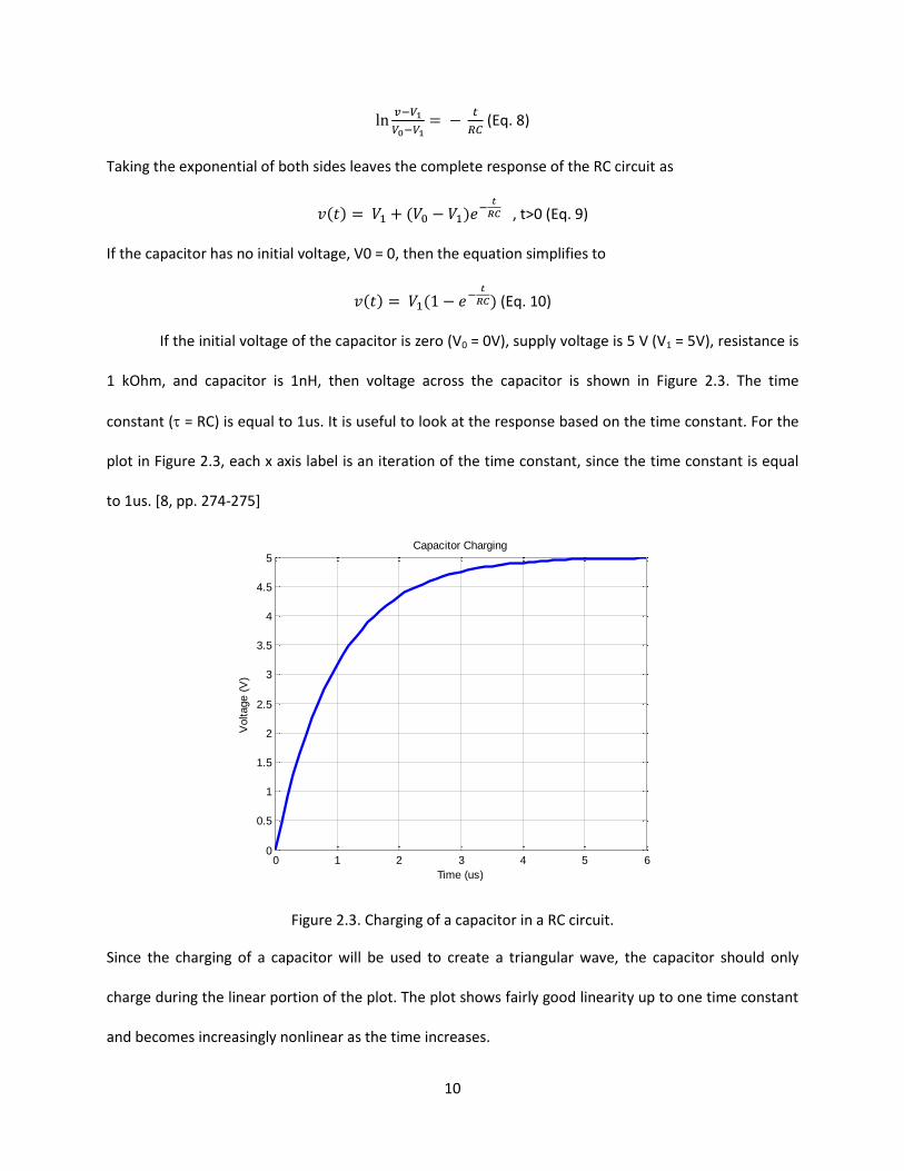
If the initial voltage of the capacitor is zero (V0 = 0V), supply voltage is 5 V (V1 = 5V), resistance is
1 kOhm, and capacitor is 1nH, then voltage across the capacitor is shown in Figure 2.3. The time
constant ( = RC) is equal to 1us. It is useful to look at the response based on the time constant. For the
plot in Figure 2.3, each x axis label is an iteration of the time constant, since the time constant is equal
to 1us. [8, pp. 274-275]
Figure 2.3. Charging of a capacitor in a RC circuit.
Since the charging of a capacitor will be used to create a triangular wave, the capacitor should only
charge during the linear portion of the plot. The plot shows fairly good linearity up to one time constant
and becomes increasingly nonlinear as the time increases.
0 1 2 3 4 5 60
0.5
1
1.5
2
2.5
3
3.5
4
4.5
5Capacitor Charging
Voltage (
V)
Time (us)

11
The capacitor will discharge when the voltage of the pulse is zero. When the pulse goes to zero,
the capacitor will have an initial voltage, V0, in the circuit shown in Figure 2.4. There is no source voltage
shown in the circuit since the voltage of the pulse is zero.
Figure 2.4. Source free RC circuit for capacitor discharging.
The current will flow through both the resistor and capacitor to ground giving the equation
𝑖𝐶 + 𝑖𝑅 = 0 (Eq. 11)
Since 𝑖𝐶 = 𝐶 𝑑𝑣
𝑑𝑡 and 𝑖𝑅 =
𝑣
𝑅 , these values can be substituted to give
𝑑𝑣
𝑑𝑡+
𝑣
𝑅𝐶= 0 (Eq. 12)
This first order differential equation can be solved resulting in the voltage of the capacitor given in
𝑣(𝑡) = 𝑉0𝑒−𝑡
𝑅𝐶 (Eq. 13)
If we plot the response of the discharging capacitor using V0 = 5V with the same resistor and
capacitor values used for the charging of the capacitor, we can see that the linear region of the response
is through one time constant as well. The plot of the discharging capacitor is shown in Figure 2.5. [8, pp.
254-256]

12
Figure 2.5. Source free RC response of the capacitor discharging voltage
Figures 2.3 and 2.5 show the way in which the capacitor charges and discharges through a single
resistor. The actual circuitry to create the triangular wave differs in that a second resistor is added in
parallel with the capacitor, shown in Figure 2.6, but the response will have the same shape as in Figures
2.3 and 2.5 only with a different slope due to the R value being different in the equations. This will
change the rate at which the capacitor charges and discharges (in turn changing the time constant), but
the linear region of the response will still remain within one time constant. The value of R for the
charging of the capacitor will be the Thevenin resistance seen by the capacitor. The value of R for the
discharging of the capacitor will be R2. Also after the first period of the triangular wave, the capacitor
will have some initial charge before the charging and the V0 for the discharge equation will be the
voltage across the capacitor after the charging time. A 555 timer will be used to create the pulse that
will be transformed into the triangular wave by the RC circuit. The design of the 555 timer will be
discussed the next chapter.
0 1 2 3 4 5 60
0.5
1
1.5
2
2.5
3
3.5
4
4.5
5Capacitor Discharging
Voltage (
V)
Time (us)

13
Figure 2.6. RC circuit used in this project to change the pulse to a triangular wave.

14
Chapter 3
Circuit and Board Design
To jam a frequency with noise, the incoming receiver must read the noise signal instead of the
desired signal from the transmitter. As stated in the Chapter 2, when the jamming signal is at the same
power level as the incoming signal (at that particular frequency) then the receiver will detect the noise
and not read the incoming desired signal. As stated in Chapter 2, certain cellular bands transmit over a
range of frequencies allotted to them and some even change this frequency throughout the call. By
jamming the entire frequency range that the cellular signal can transmit, then jamming of the desired
signal no matter which frequency (in the particular communication standard) or whether or not the
frequency hops can be achieved. Jamming the entire frequency band of the cellular network requires a
large bandwidth of noise being produced.
For this work, we will look at jamming two different frequencies bands, CDMA850 and GSM900,
which correlate to 851-894MHz and 925-960MHz respectively. These frequencies are the downlink
frequencies from the base station to the cellular receiver, which is all that is required to jam the service.
These two frequency bands are 2G and used on most phones available on the market, even the 3G and
4GLTE phones. On the 3G and 4GLTE phones, when the phones do not have 3G and 4GLTE service these
2G frequencies will be used. To completely jam a phone with 3G and 4GLTE, a jamming signal must be
created for each of the frequency bands that the phone operates. The remainder of this chapter will
discuss the circuit design and board design for the creation of the jamming signal.

15
3.1 Overview of Frequency Jammer Design
For the design of the frequency jammer, there are four necessary sections of the design as
shown in the block diagram in Figure 3.1. The most importantly part of the design is the RF section. This
section contains the VCO, which is the backbone of the entire system. The RF section also contains the
amplifier that will increase the jamming signal to the necessary power levels. The tuning circuitry creates
the tuning voltage signal that is to be fed to the tuning input of the VCO. Since the VCO depends on this
tuning circuitry, the tuning circuitry design will be discussed alongside the RF section in Section 3.2, RF
Circuitry. The remaining two sections of the frequency jammer design are the power supply and
antenna. The power supply simply produces the necessary voltage rails that the design tuning circuitry
and RF section require while the antenna section transmits the signal leaving the amplifier into the
wireless jamming signal. Each part of the frequency jammer will be discussed in more detail in the
following sections.
Figure 3.1. Simple block diagram of a single band frequency jammer.
3.2 RF Circuitry
The RF circuitry in this design of a frequency jammer starts with the VCO. While it is possible to
create the VCOs for these frequency ranges, there are widely available VCOs that operate in the desired
frequency ranges. The two VCOs being used in this design are ROS-892-119+ and ROS-1000PV from
Power
Supply
RF Section
Antenna
Tuning Circuit
16
MiniCircuits, which cover the CDMA and GSM frequency ranges respectively. From the ROS-892-119+
data sheet, 851MHz corresponds to a tuning voltage of approximately 2V and 894 MHz corresponds to a
tuning voltage of approximately 3.5V [9]. From the ROS-1000PV datasheet, 925 MHz corresponds to a
tuning voltage of approximately 2V and 960 MHz corresponds to a tuning voltage of approximately 3V
[10]. Noise must be added to the input of the VCO so the noise is modulated onto the carrier signal that
the VCO produces. For the jamming signal to cover the entire GSM900 and CDMA850 standard, the
input tuning signal (with noise) must range from the voltages that correspond to the frequencies of each
VCO that were previously stated. The ways to achieve the tuning signal will be discussed in the
remainder of this Section 3.2.
3.2.1 VCO Tuning Signal Using Only Noise
The first way to get the necessary voltage for each input tuning signal is for the tuning signal to
be a large amplitude of noise that ranges from the VCO tuning voltages that correspond to the upper
and lower frequencies of the necessary spectrum. Since the design of the jammer requires the jamming
signal to be noise, using only noise at the VCO input will modulate the carrier signal with a large
bandwidth of noise. The larger the amplitude of noise at the input of the VCO will result in a larger
bandwidth of noise being modulated onto the carrier signal. The creation of the noise tuning signal can
be accomplished with a noise generator along with a DC bias to shift the noise up to the necessary level.
The DC bias and noise generator voltages will be combined through an operational amplifier circuit. It
should be noted that there will be some loss through the operational amplifier circuit, so the amplitudes
entering the operational amplifier must be slightly larger than what is needed at the VCO. The schematic
for the noise generator and DC bias is shown in Figure 3.2. The noise generator circuit used was found
from SiliconChip.com [11]. The output amplitude of the noise generator is adjusted through a voltage

17
divider consisting of R22 and the potentiometer RV1. The potentiometer chosen for this design ranges
up to 10K and allows for the amplitude of the noise to be adjusted to a level that is suitable. If the
amplitude of the noise is not large enough when the potentiometer is turn to its highest resistance, then
the R22 value can be decreased so that the potentiometer has a greater effect in the voltage divider.
The DC bias consists of a voltage divider with a potentiometer, RV6, so that the DC voltage can be
changed to raise or lower the noise amplitude at the input of the VCO.
Figure 3.2. Schematic of the noise generator, DC bias, and operational amplifier circuit.
3.2.2 VCO Tuning Signal Using a Triangular Wave
Another way to produce the full bandwidth of noise needed out of the VCO is to sweep a
bandwidth of noise (less than the full bandwidth of the spectrum) back and forth across the frequency
spectrum. This can be accomplished by putting a small amplitude of noise onto a triangular wave that

18
has a minimum and maximum voltage that corresponds to the needed tuning voltage of the VCO. There
are different ways to produce this triangular wave, and for this paper we will look at using a 555 timer to
produce a pulse waveform that will be transformed to a triangular wave through a resistor and capacitor
network. The 555 timer being used for this is the TLC555IDR from Texas Instruments. The 555 timer was
chosen due to ability to produce a pulse frequency up to 2 MHz, so that numerous frequencies of the
triangular tuning wave can be tested.
The TLC555IDR can be operated in three different ways, which are monostable, bistable, and astable.
Due to the design’s need for a continuous triangular wave, the 555 timer will operate in astable mode.
The layout schematic of the 555 timer in astable mode is shown in Figure 3.3 with the RC network to
transform the pulse into a triangular wave. In this mode the capacitor C1 charges through R1 and R2 to
the threshold voltage and then discharges through R2 to the trigger voltage level. This will cause the
output of the 555 timer to be high (typically 4.8 V with a VCC of 5 V) while the capacitor charges and low
while the capacitor discharges. The duty cycle of the output is therefore controlled by R1, R2, and C1. The
equations for charge time, discharge time, and duty cycle are shown below in equations 14, 15, and 16
respectively. These equations are just an approximation since they do not allow for any propagation
delay times from the TRIG and THRES inputs to DISCH. Also the capacitor connected to CONT input
decreases the period by approximately 10% [12].
𝑡𝑐(𝐻)≈𝐶1(𝑅1+𝑅2)ln (2) (Eq. 14)
𝑡𝑐(𝐿)≈𝐶1𝑅2ln (2) (Eq. 15)
𝑂𝑢𝑡𝑝𝑢𝑡 𝑤𝑎𝑣𝑒𝑓𝑜𝑟𝑚 𝑑𝑢𝑡𝑦 𝑐𝑦𝑐𝑙𝑒 = 𝑡𝑐(𝐻)
𝑡𝑐(𝐻)+𝑡𝑐(𝐿) (Eq. 16)
From equation 14 and 15 the frequency of the output pulse can also be calculated by
𝑓𝑝𝑢𝑙𝑠𝑒 = 1
𝑡𝑐(𝐻)+𝑡𝑐(𝐿) (Eq. 17)

19
Once the output pulse of the 555 timer is generated, it needs to be transformed into a triangular
wave. To do this the pulse is fed into a voltage divider in parallel with a capacitor, which is
included in Figure 3.3. The capacitor, C3, charges when the pulse is high and discharges when
the pulse is low in the manner discussed in section 2.6.
Figure 3.3. Schematic of 555 timer in astable mode with RC network for creation of triangular wave.
This triangular wave that is produced by using the 555 timer must have the correct peak to peak voltage
to span the necessary minimum and maximum voltages required by the VCO. Since the Vmax and Vmin of
the triangular wave needs to be raised to equal what is needed by the VCO, a DC bias will be applied.
Also noise must be applied to the wave so that it will be modulated onto the carrier signal. For these
reasons, the triangular wave is added to the operational amplifier circuit to combine with the DC bias
and noise generator output to complete the tuning circuitry with a triangular wave. The schematic for
the tuning circuitry with a triangular wave is shown below in Figure 3.4. A test point is located at the
output of the 555 timer and RC network so the triangular wave can be seen.
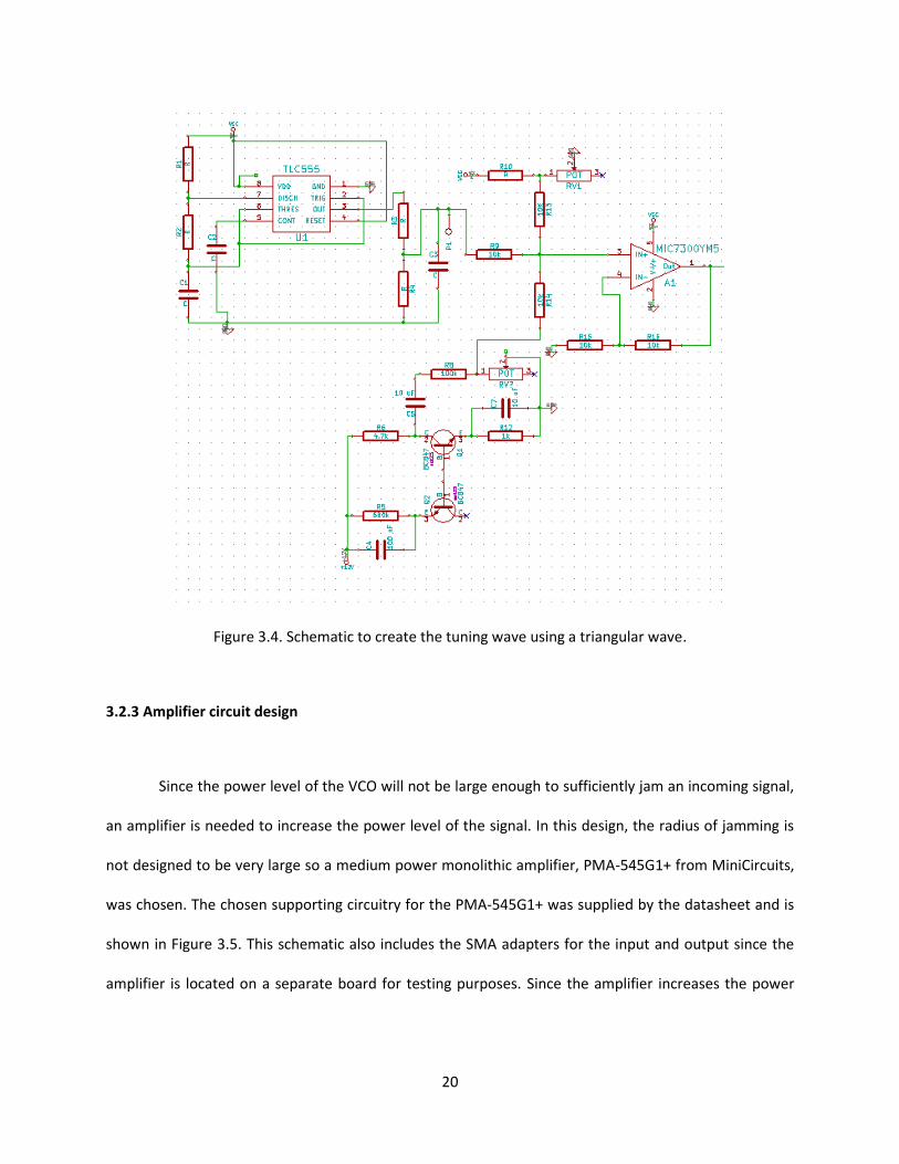
20
Figure 3.4. Schematic to create the tuning wave using a triangular wave.
3.2.3 Amplifier circuit design
Since the power level of the VCO will not be large enough to sufficiently jam an incoming signal,
an amplifier is needed to increase the power level of the signal. In this design, the radius of jamming is
not designed to be very large so a medium power monolithic amplifier, PMA-545G1+ from MiniCircuits,
was chosen. The chosen supporting circuitry for the PMA-545G1+ was supplied by the datasheet and is
shown in Figure 3.5. This schematic also includes the SMA adapters for the input and output since the
amplifier is located on a separate board for testing purposes. Since the amplifier increases the power
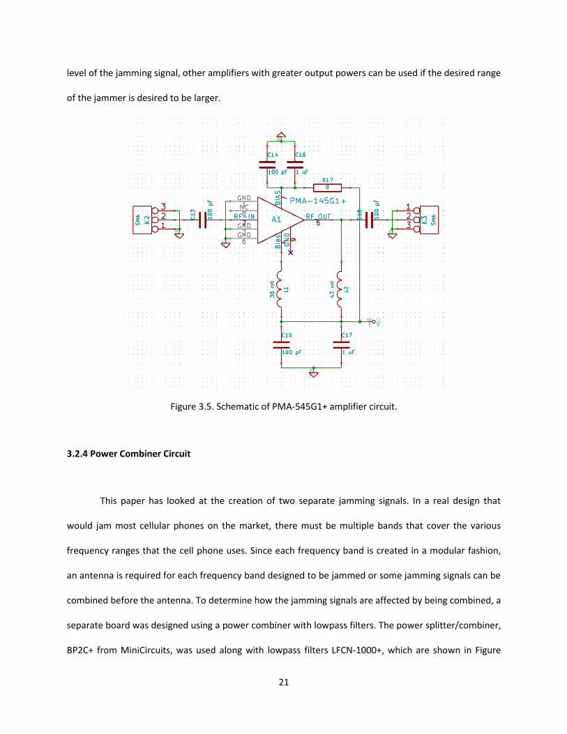
21
level of the jamming signal, other amplifiers with greater output powers can be used if the desired range
of the jammer is desired to be larger.
Figure 3.5. Schematic of PMA-545G1+ amplifier circuit.
3.2.4 Power Combiner Circuit
This paper has looked at the creation of two separate jamming signals. In a real design that
would jam most cellular phones on the market, there must be multiple bands that cover the various
frequency ranges that the cell phone uses. Since each frequency band is created in a modular fashion,
an antenna is required for each frequency band designed to be jammed or some jamming signals can be
combined before the antenna. To determine how the jamming signals are affected by being combined, a
separate board was designed using a power combiner with lowpass filters. The power splitter/combiner,
BP2C+ from MiniCircuits, was used along with lowpass filters LFCN-1000+, which are shown in Figure
22
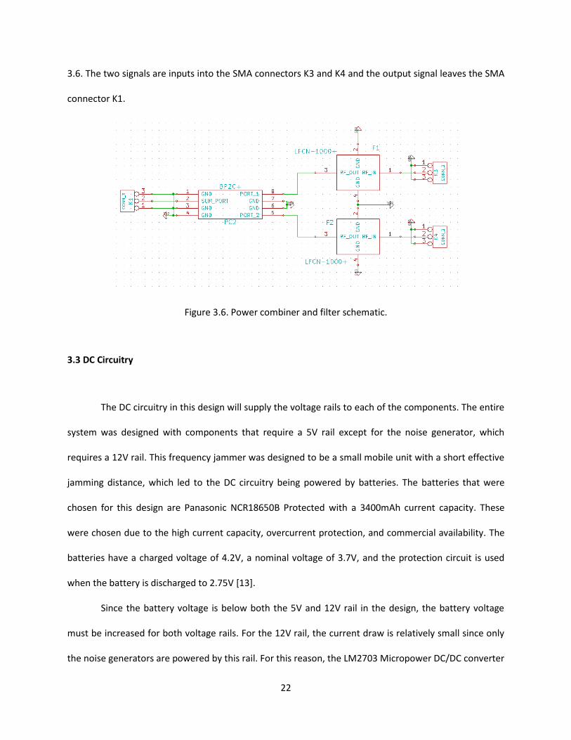
3.6. The two signals are inputs into the SMA connectors K3 and K4 and the output signal leaves the SMA
connector K1.
Figure 3.6. Power combiner and filter schematic.
3.3 DC Circuitry
The DC circuitry in this design will supply the voltage rails to each of the components. The entire
system was designed with components that require a 5V rail except for the noise generator, which
requires a 12V rail. This frequency jammer was designed to be a small mobile unit with a short effective
jamming distance, which led to the DC circuitry being powered by batteries. The batteries that were
chosen for this design are Panasonic NCR18650B Protected with a 3400mAh current capacity. These
were chosen due to the high current capacity, overcurrent protection, and commercial availability. The
batteries have a charged voltage of 4.2V, a nominal voltage of 3.7V, and the protection circuit is used
when the battery is discharged to 2.75V [13].
Since the battery voltage is below both the 5V and 12V rail in the design, the battery voltage
must be increased for both voltage rails. For the 12V rail, the current draw is relatively small since only
the noise generators are powered by this rail. For this reason, the LM2703 Micropower DC/DC converter

23
was chosen to increase the battery voltage to 12V. This DC/DC converter requires an input voltage from
2.2V to 7V and produces an output voltage up to 21V that can be adjusted based on the components
that are used with the LM2703. The schematic for the 12V rail is shown in Figure 3.7. This voltage rail
does not need to be very accurate since the voltage is only needed to be 12V or higher to cause the
transistor to breakdown to supply noise.
Figure 3.7. Schematic of 12V boost circuitry.
The 5V rail will draw a much higher current than the 12V rail since the majority of the
components are powered from the 5V rail. Although we are only testing two bands with medium
powered amplifiers, the 5V rail was designed so that numerous bands can be added and/or adding
higher powered amplifiers if these amplifiers do not sufficiently produce the power needed to jam the
desired distance. The FAN48630UC50X boost regulator from Fairchild was chosen to step up the voltage
from the battery to 5V. The input voltage range for this boost converter is from 2.35V to 5.5V. Also the
output current capacity was 1500mA at and efficiency up to 96%. Since the max current capacity was
1.5A, it was decided supply the 5V rail with two of the FAN48630U50X converters in parallel to provide
up to a possible 3A to the components in the design on the 5V rail. The 3A current capacity was
determined to be more than sufficient in this design, which would be able to power six bands using the
same amplifiers for well over an hour. The two 5V boost converters and the supporting circuitry is
shown in Figure 3.8.
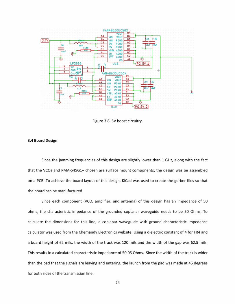
24
Figure 3.8. 5V boost circuitry.
3.4 Board Design
Since the jamming frequencies of this design are slightly lower than 1 GHz, along with the fact
that the VCOs and PMA-545G1+ chosen are surface mount components; the design was be assembled
on a PCB. To achieve the board layout of this design, KiCad was used to create the gerber files so that
the board can be manufactured.
Since each component (VCO, amplifier, and antenna) of this design has an impedance of 50
ohms, the characteristic impedance of the grounded coplanar waveguide needs to be 50 Ohms. To
calculate the dimensions for this line, a coplanar waveguide with ground characteristic impedance
calculator was used from the Chemandy Electronics website. Using a dielectric constant of 4 for FR4 and
a board height of 62 mils, the width of the track was 120 mils and the width of the gap was 62.5 mils.
This results in a calculated characteristic impedance of 50.05 Ohms. Since the width of the track is wider
than the pad that the signals are leaving and entering, the launch from the pad was made at 45 degrees
for both sides of the transmission line.

25
3.4.1 KiCad Overview
KiCad uses 4 different tools to go from a schematic to board layout, which are Eeschema, Cvpcb,
Pcbnew, and Gerberview. In Eeschema the electronic schematic can be created by placing and wiring
the components of the design. There are additional component libraries provided by KiCad that will
contain many of the parts that are needed, although there is a high likelihood that it will not contain all
the needed components. If this is the case, individual components can be created in Eeschema. The
netlist file that contains the connections of the circuit is also created in Eeschema that will be used later
in the KiCad process.
Once the schematic has been created, the Cvpcb tool uses the netlist file to match the layout
footprint with the component in the schematic. There are also libraries for this tool that contain many of
the generic smd packages, but additional footprints can be created in Pcbnew if necessary. After the
schematic component has been assigned the particular layout footprint, the netlist can be loaded into
the Pcbnew tool so that the physical layout of the parts can be placed on the PCB. After the footprints
are correctly placed, the gerber files that are created can be checked in Gerberview before they are sent
to a manufacturer to be fabricated.
3.4.2 Multiple Boards for Testing
The design of the boards for this paper took into account the need to measure the signals at
multiple stages of the design. For this reason, the design was separated into separate boards: VCO and
tuning circuit board, amplifier board, antenna board, power combiner board, and the DC power supply
board.
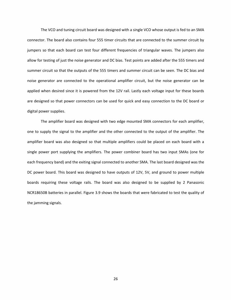
26
The VCO and tuning circuit board was designed with a single VCO whose output is fed to an SMA
connector. The board also contains four 555 timer circuits that are connected to the summer circuit by
jumpers so that each board can test four different frequencies of triangular waves. The jumpers also
allow for testing of just the noise generator and DC bias. Test points are added after the 555 timers and
summer circuit so that the outputs of the 555 timers and summer circuit can be seen. The DC bias and
noise generator are connected to the operational amplifier circuit, but the noise generator can be
applied when desired since it is powered from the 12V rail. Lastly each voltage input for these boards
are designed so that power connectors can be used for quick and easy connection to the DC board or
digital power supplies.
The amplifier board was designed with two edge mounted SMA connectors for each amplifier,
one to supply the signal to the amplifier and the other connected to the output of the amplifier. The
amplifier board was also designed so that multiple amplifiers could be placed on each board with a
single power port supplying the amplifiers. The power combiner board has two input SMAs (one for
each frequency band) and the exiting signal connected to another SMA. The last board designed was the
DC power board. This board was designed to have outputs of 12V, 5V, and ground to power multiple
boards requiring these voltage rails. The board was also designed to be supplied by 2 Panasonic
NCR18650B batteries in parallel. Figure 3.9 shows the boards that were fabricated to test the quality of
the jamming signals.

27
(a)
(b)
28
(c)
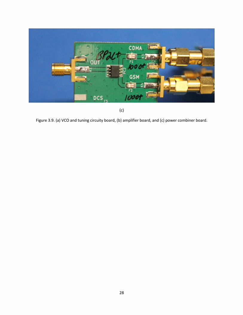
Figure 3.9. (a) VCO and tuning circuity board, (b) amplifier board, and (c) power combiner board.

29
Chapter 4
Measurements of the Jamming Signal
In this chapter we discuss the ways in which the jamming signal was created and characterize
the signal based on two factors: the power level and uniformity of the jamming signal. The quality of the
jamming signal will be tested at the output of the VCO and amplifier. The measurements that are taken
in the chapter were acquired by a DSA-X 93204A Digital Signal Analyzer from Agilent Technologies with
the built in FFT algorithm using a 200 us capture time and a sampling rate of 5 GS/s.
4.1 Response to a Single Tone
The creation of the jamming signal by the VCO is the most important instance in the entire
design. Since it is desired that the jamming signal cover the entire bandwidth of the GSM900 and
CDMA850 standard, it is needed to know how the VCO reacts to the bandwidth being produced. To
determine how the VCO reacts to the creation of a bandwidth of noise, the VCO output must be
characterized for a single tone when only a DC voltage is applied to the tuning input. The output of the
single tone from the CDMA and GSM VCOs is shown in Figure 4.1. The single tone of the VCO occurs
when no noise is added through the operational amplifier to the DC bias so only a single voltage from
the DC bias is applied to the tuning input of the VCO.
30
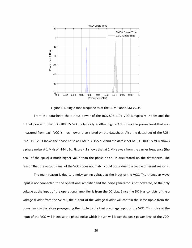
Figure 4.1. Single tone frequencies of the CDMA and GSM VCOs.
From the datasheet, the output power of the ROS-892-119+ VCO is typically +4dBm and the
output power of the ROS-1000PV VCO is typically +6dBm. Figure 4.1 shows the power level that was
measured from each VCO is much lower than stated on the datasheet. Also the datasheet of the ROS-
892-119+ VCO shows the phase noise at 1 MHz is -155 dBc and the datasheet of ROS-1000PV VCO shows
a phase noise at 1 MHz of -144 dBc. Figure 4.1 shows that at 1 MHz away from the carrier frequency (the
peak of the spike) a much higher value than the phase noise (in dBc) stated on the datasheets. The
reason that the output signal of the VCOs does not match could occur due to a couple different reasons.
The main reason is due to a noisy tuning voltage at the input of the VCO. The triangular wave
input is not connected to the operational amplifier and the noise generator is not powered, so the only
voltage at the input of the operational amplifier is from the DC bias. Since the DC bias consists of the a
voltage divider from the 5V rail, the output of the voltage divider will contain the same ripple from the
power supply therefore propagating the ripple to the tuning voltage input of the VCO. This noise at the
input of the VCO will increase the phase noise which in turn will lower the peak power level of the VCO.
0.8 0.82 0.84 0.86 0.88 0.9 0.92 0.94 0.96 0.98 1-60
-50
-40
-30
-20
-10
0
10VCO Single Tone
Frequency (GHz)
Pow
er
Level (d
Bm
)
CMDA Single Tone
GSM Single Tone

31
Since the goal of the design is to create a noisy jamming signal, there was no need to filter out the ripple
on the DC bias voltage because additional noise will be added for the measurements of the jamming
signal.
Some of the power loss could also be attributed to reflection through the CPW and SMA
connector. While the CPW was designed for 50 Ohm characteristic impedance, the launch to the needed
width and the tolerance of manufacturing could lead to a different characteristic impedance that will
induce reflection of the signal which will drop the power that is transmitted through the SMA. The
power loss due to any reflection would not be the primary cause for the power loss unless the majority
of the signal is reflected, which would imply that the major reason for the power loss and additional
phase noise is due to the noise on the tuning input to the VCO.
Even though this power level is not as high as the datasheet states for a single tone, this is not
that big of an issue for the rest of the design. The loss in power due to the noise on the tuning voltage
will not be an issue since additional noise will be added to create the jamming signal and the
transmission line can be optimized to reduce any reflection.
Along with testing the VCO output for a single tone, the output of the amplifier must also be
tested for the same signal. For this design, the PMA-545G1+ amplifier was chosen so that the output
power would be high enough to jam a short area around the device. Other amplifiers with a higher
output power can be chosen for greater range, but for this design a higher power level is not needed.
The amplified single tones are shown in Figure 4.2.

32
Figure 4.2. Amplification of single tones by PMA-545G1+.
The datasheet of the amplifier states that the typical output power is +22 dBm at 900 MHz,
whereas Figure 4.2 shows that the output power is lower than the stated value from the datasheet.
Figure 4.2 also shows that the peak power level of both VCOs are very close together with the CDMA
signal’s power level being slightly lower. This shows that the gain of the CDMA signal is larger than the
gain of the GSM signal which indicates that the amplifier of the GSM signal (and possibly amplifier for
the CDMA signal) has supplied the maximum power instead of the maximum gain. It is possible that the
reason the power levels out of the amplifiers are less than stated in the datasheet can be attributed to
the same reasons as the VCOs power level being less than the power stated on the datasheets. The
power levels shown in Figure 4.2 will give a base for comparison for jamming signal that covers the
desired frequency range.
0.8 0.82 0.84 0.86 0.88 0.9 0.92 0.94 0.96 0.98 1-60
-50
-40
-30
-20
-10
0
10
20
Frequency (GHz)
Pow
er
Level (d
Bm
)
Amp Gain Single Tone
CDMA Amp Output
CDMA VCO Output
GSM Amp Output
GSM VCO Output
33
4.2 Increasing Bandwidth using Noise
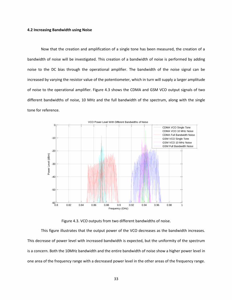
Now that the creation and amplification of a single tone has been measured, the creation of a
bandwidth of noise will be investigated. This creation of a bandwidth of noise is performed by adding
noise to the DC bias through the operational amplifier. The bandwidth of the noise signal can be
increased by varying the resistor value of the potentiometer, which in turn will supply a larger amplitude
of noise to the operational amplifier. Figure 4.3 shows the CDMA and GSM VCO output signals of two
different bandwidths of noise, 10 MHz and the full bandwidth of the spectrum, along with the single
tone for reference.
Figure 4.3. VCO outputs from two different bandwidths of noise.
This figure illustrates that the output power of the VCO decreases as the bandwidth increases.
This decrease of power level with increased bandwidth is expected, but the uniformity of the spectrum
is a concern. Both the 10MHz bandwidth and the entire bandwidth of noise show a higher power level in
one area of the frequency range with a decreased power level in the other areas of the frequency range.
0.8 0.82 0.84 0.86 0.88 0.9 0.92 0.94 0.96 0.98 1-60
-50
-40
-30
-20
-10
0
Frequency (GHz)
Pow
er
Level (d
Bm
)
VCO Power Level With Different Bandwidths of Noise
CDMA VCO Single Tone
CDMA VCO 10 MHz Noise
CDMA Full Bandwidth Noise
GSM VCO Single Tone
GSM VCO 10 MHz Noise
GSM Full Bandwidth Noise

34
This is a problem if the frequency to be jammed is not known and therefore can be located in the area of
the spectrum with the lower power of the jamming signal. For the design to jam an unknown frequency,
the lowest power level of the spectrum is the limiting factor in its effectiveness. Since the jamming
signal must be amplified, Figure 4.4 shows the amplification of the entire bandwidth of noise.
Figure 4.4. Amplification of full bandwidth of noise using only noise in the tuning signal.
As expected, the output spectrums from the amplifiers have the same issues regarding the
uniformity of the spectrum. While the spectrum still has a higher power level towards the center of the
spectrum, the entire spectrum also changes slightly from the VCO measurement to the amplifier
measurement. The reason for this change is due to the way that the noise on the input tuning signal
interacts with the VCO. Since the noise will constantly change at the input of the VCO, the output of the
VCO will also change with the noise on the tuning signal. This output of the VCO will not drastically alter
the jamming signal, but there will be slight differences to the output spectrum throughout the duration
of signal. This change can be seen in the CDMA signal, in which the VCO output has a more linear slope
than the amplifier output.
0.8 0.82 0.84 0.86 0.88 0.9 0.92 0.94 0.96 0.98 1-60
-50
-40
-30
-20
-10
0
10VCO and AMP Output Full Bandwidth of Noise
Frequency (GHz)
Pow
er
Level (d
Bm
)
CDMA Amp Output Full Bandwidth
CDMA VCO Output Full Bandwidth
GSM Amp Output Full Bandwidth
GSM VCO Output Full Bandwidth

35
Along with the slight changes in the continuity of the output spectrum, Figure 4.4 also shows
how the amplifier responds to the large bandwidth of noise. It can be seen that the peak power level of
the amplified jamming signal are about the same for both CDMA and GSM. This shows that the amplifier
is reaching the maximum output power it can generate for both signals, such as was the case with the
amplification of the single tone. Even though the amplifier is maxing out the power level, the gain of the
entire frequency range is lower with the large bandwidth of noise than the single tone. For the single
tone, the gain of the CDMA and GSM signals is approximately 24 dB and 20 dB respectively from Figure
4.2. Due to the random spikes around the peaks in Figure 4.4, it is harder to see what the actual gain for
the full bandwidth of noise, but it appears to be around 14 dB for the CDMA spectrum and 10 dB for the
GSM spectrum. This shows that the addition of the bandwidth of noise decreases the gain that can be
achieved by the amplifier while delivering the maximum output power.
While the change in gain do to the addition of noise is something to be examined, the desire to
create the jamming signal with a more uniform power level should be examined first.
4.3 Jamming Using Noise Added to a Triangular Wave
The creation of the jamming signal across the entire bandwidth of the GSM and CDMA
spectrums was accomplished using noise added to the DC bias. This was successful in creating the
desired bandwidth; however, the uniformity of the power level is poor and will decrease the
effectiveness to the lowest power level in the desired frequency range. For this reason, it was decided
to investigate the output spectrum of the VCO and amplifier when the noise is applied to a triangular
wave where the minimum and maximum voltages of the triangular wave correspond to the low and high
end frequencies of the desired jamming signal. By using a triangular wave, a bandwidth of noise will be
swept across the desired frequency range. In this section the jamming signal will be tested with three

36
different variables: the frequency of the triangular wave, the bandwidth of noise added to the triangular
wave, and the frequency range of the jamming signal.
4.3.1 Frequency of the Triangular Wave
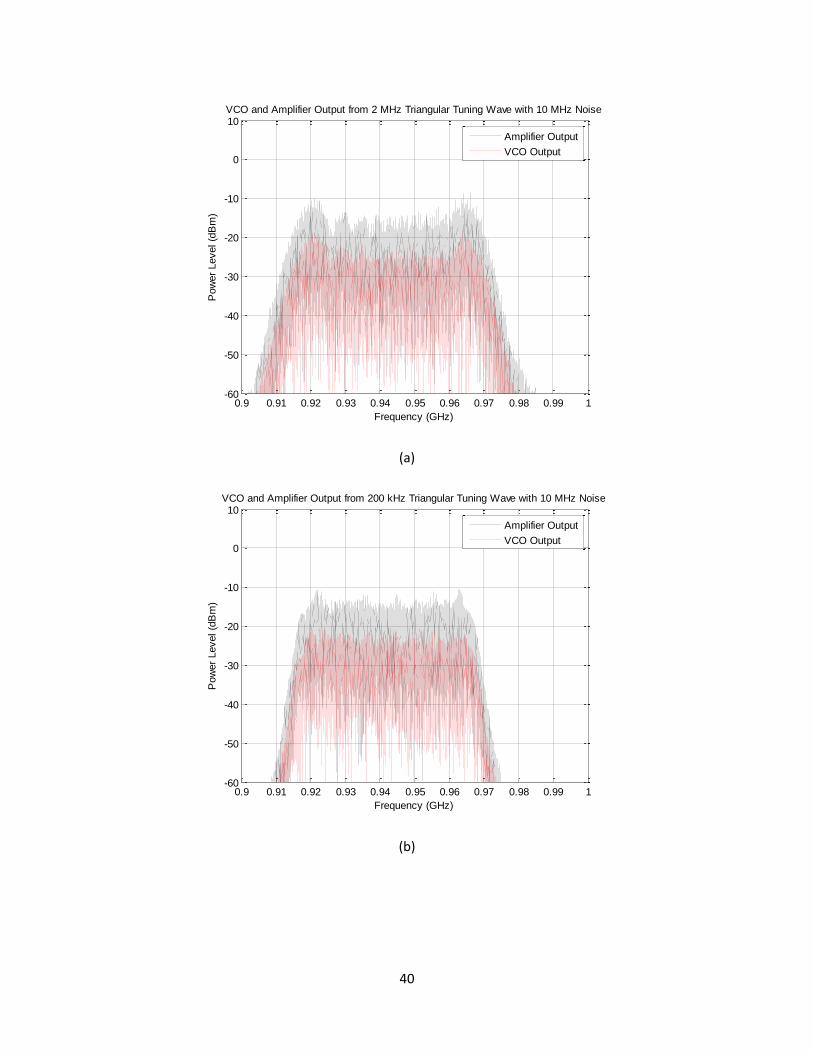
By using a triangular wave to sweep a bandwidth of noise across the spectrum, it is important to
determine how the frequency of the triangular wave affects the output spectrum of the VCO and
amplifier. It was decided to initially test four different frequencies that differ in an order of magnitude
with the GSM VCO. These frequencies are 2 MHz, 200 kHz, 20 kHz, and 2 kHz. To achieve these
frequencies, the resistor and capacitor values of R1, R2, and C1 from Figure 3.3 that control the
frequency of the 555 timers are shown in Table 1. The component values will not produce the exact
targeted frequency, but the frequencies are very close to the desired frequency. Figure 4.5 shows the
VCO and amplifier outputs of the four different tuning frequencies without having noise applied to the
triangular wave.
Resistor and Capacitor Values That Control Frequency of 555 Pulse
Frequency R1 R2 C1
2 MHz 300 1 k 68 pF
200 kHz 1 k 12 k 240 pF
20 kHz 3.3 k 82 k 360 pF
2 kHz 12 k 909 k 360 pF
Table 4.1. R1, R2, and C1 values that control the frequencies of the 555 timers used to test the ROS-1000PV VCO.

37
(a)
(b)
0.9 0.91 0.92 0.93 0.94 0.95 0.96 0.97 0.98 0.99 1-60
-50
-40
-30
-20
-10
0
10VCO and Amplifier Output with 2 MHz Triangular Tuning Wave
Frequency (GHz)
Pow
er
Level (d
Bm
)
Amplifier Output
VCO Output
0.9 0.91 0.92 0.93 0.94 0.95 0.96 0.97 0.98 0.99 1-60
-50
-40
-30
-20
-10
0
10VCO and Amplifier Output with 200 kHz Triangular Tuning Wave
Frequency (GHz)
Pow
er
Level (d
Bm
)
Amplifier Output
VCO Output

38
(c)
(d)
Figure 4.5. VCO and amplifier output spectrums of the (a) 2 MHz, (b) 200 kHz, (c) 20 kHz, and (d) 2 kHz
triangular wave tuning signals with no noise.
0.9 0.91 0.92 0.93 0.94 0.95 0.96 0.97 0.98 0.99 1-60
-50
-40
-30
-20
-10
0
10VCO and Amplifier Output with 20 kHz Triangular Tuning Wave
Frequency (GHz)
Pow
er
Level (d
Bm
)
Amplifier Output
VCO Output
0.9 0.91 0.92 0.93 0.94 0.95 0.96 0.97 0.98 0.99 1-60
-50
-40
-30
-20
-10
0
10VCO and Amplifier Output with 2 kHz Triangular Tuning Wave
Frequency (GHz)
Pow
er
Level (d
Bm
)
Amplifier Output
VCO Output

39
The plots in Figure 4.5 show how the VCO and amplifier react to varying frequencies of the
tuning wave without noise. It can be seen that for the 2 MHz tuning wave, the output has only spikes
throughout the spectrum with the signal having gaps through most of the spectrum. This leads us to
believe that the VCO cannot keep up with the speed of the triangular wave. The 200 kHz signal also
shows the same voids in the spectrum, but the voids in the spectrum are much smaller than that of the
2 MHz signal. With the 20 kHz signal, the coverage is full showing that the VCO can respond quickly
enough at this frequency. The last frequency tested, the 2 kHz triangular wave, is too slow to produce
the full bandwidth of noise needed for the spectrum. While the capture time of the plots, 200 us, is less
than the time needed to transmit data in the GSM and CDMA standard, we will consider the 2 kHz signal
too slow for the VCO to create full bandwidth jamming signal in the time needed to be present for the
entirety of an incoming CDMA and GSM communication signal.
The plots shown in Figure 4.5 show that the 2 MHz and 200 kHz signal show voids throughout
the spectrum of the jamming signal. This is the case with no noise added to triangular wave; but since
noise must be modulated onto the jamming signal, the noise must be added to the triangular wave
before the 2 MHz and 200 kHz signal can be determined as inefficient. Figure 4.6 shows the 2 MHz, 200
kHz, 20 kHz, and 2 kHz triangular tuning waves with a 10 MHz bandwidth of noise added to the
triangular wave.
40
(a)
(b)
0.9 0.91 0.92 0.93 0.94 0.95 0.96 0.97 0.98 0.99 1-60
-50
-40
-30
-20
-10
0
10VCO and Amplifier Output from 2 MHz Triangular Tuning Wave with 10 MHz Noise
Frequency (GHz)
Pow
er
Level (d
Bm
)
Amplifier Output
VCO Output
0.9 0.91 0.92 0.93 0.94 0.95 0.96 0.97 0.98 0.99 1-60
-50
-40
-30
-20
-10
0
10VCO and Amplifier Output from 200 kHz Triangular Tuning Wave with 10 MHz Noise
Frequency (GHz)
Pow
er
Level (d
Bm
)
Amplifier Output
VCO Output

41
(c)
(d)
Figure 4.6. VCO and amplifier output spectrums of the (a) 2 MHz, (b) 200 kHz, (c) 20 kHz, and (d) 2 kHz
triangular wave tuning signals with 10 MHz of noise added.
0.9 0.91 0.92 0.93 0.94 0.95 0.96 0.97 0.98 0.99 1-60
-50
-40
-30
-20
-10
0
10VCO and Amplifier Output from 20 kHz Triangular Tuning Wave with 10 MHz Noise
Frequency (GHz)
Pow
er
Level (d
Bm
)
Amplifier Output
VCO Output
0.9 0.91 0.92 0.93 0.94 0.95 0.96 0.97 0.98 0.99 1-60
-50
-40
-30
-20
-10
0
10VCO and Amplifier Output from 2 kHz Triangular Tuning Wave with 10 MHz Noise
Frequency (GHz)
Pow
er
Level (d
Bm
)
Amplifier Output
VCO Output

42
The addition of noise onto the triangular tuning wave changes the output spectrum quite
dramatically, especially the 2 MHz and 200 kHz triangular tuning waves. With the addition of noise, the
spikes in the spectrum from the 2 MHz and 200 kHz triangular tuning waves have been smoothed over
to fill in the voids that were in the spectrum. While the addition of the noise helped the 2 MHz signal,
there are still some peaks and valleys in the output spectrum. These slight peaks and valleys cause the
effective power of the jamming signal to be less than the effective power of the jamming signal using
the 200 kHz triangular wave. The output spectrum from the 200 kHz triangular tuning wave shows
smaller spikes that appear to be similar to the spikes created in the spectrum of Figure 4.3 and Figure
4.4, which are caused by the noise that is modulated onto the carrier signal. These spikes in the
spectrum are not ideal, but will occur do to the constant changes in the amplitude of noise being applied
to the tuning signals. The output spectrum form the 20 kHz triangular tuning wave show similar but
more drastic spikes as that of the output spectrum from the 200 kHz triangular tuning wave. As with the
spectrum from the 2 kHz triangular tuning wave with no noise added, the spectrum from the 2 kHz
triangular tuning wave does not sufficiently cover the desired spectrum in the time needed.
Aside from the peaks and valleys in the spectrum from the 2 MHz triangular tuning wave and
the spikes in the spectrum from the 200 kHz and 20 kHz triangular tuning waves, the output power level
is much more uniform across the full spectrum than the jamming signal created without a triangular
wave. Comparing the spectrums from the 2 MHz, 200 kHz, and 20 kHz triangular tuning waves, it can be
seen that the spectrum from the 200 kHz tuning wave has the most uniform spectrum at the highest
power level. This highest power level across the entire jamming signal, approximately -15 dBm, is much
higher than lowest part of the spectrum created from only noise in Figure 4.4, which is somewhere
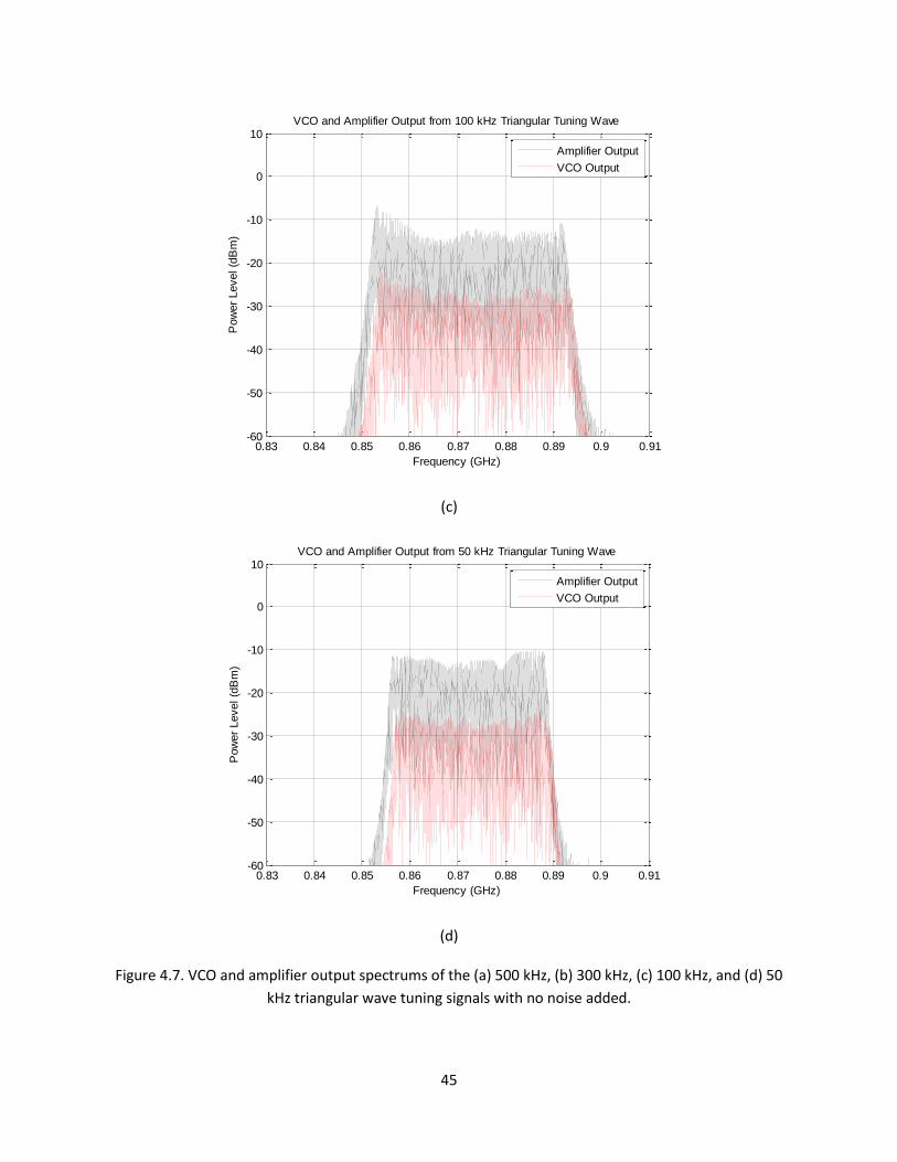
between -25 and -30 dBm. Since the 200 kHz tuning wave showed the best result, additional
frequencies were tested using the CDMA VCO. These frequencies tested were 500 kHz, 300 kHz, 100
kHz, and 50 kHz so to test the frequencies around the 200 kHz. The resistor and capacitor values of R1,

43
R2, and C1 from Figure 3.3 that control the frequency of the 555 timers are shown in Table 2. As with
the frequencies tested with the ROS-1000PV VCO, the component values will not produce the exact
targeted frequency, but the frequencies are very close to the desired frequency. Figure 4.7 shows the
500 kHz, 300 kHz, 100 kHz, and 50 kHz tuning frequencies without any noise being added to the wave,
while Figure 4.8 shows those frequencies of tuning waves with the 10 MHz of noise needed to modulate
the noise onto the carrier signal.
Resistor and Capacitor Values That Control Frequency of 555 Pulse
Frequency R1 R2 C1
500 kHz 500 9 k 68 pF
300 kHz 500 9 k 240 pF
100 kHz 1 k 25 k 360 pF
50 kHz 2 k 55 k 360 pF
Table 4.2. R1, R2, and C1 values that control the frequencies of the 555 timers used to test the ROS-892-119+ VCO.

44
(a)
(b)
0.83 0.84 0.85 0.86 0.87 0.88 0.89 0.9 0.91-60
-50
-40
-30
-20
-10
0
10VCO and Amplifier Output from 500 kHz Triangular Tuning Wave
Frequency (GHz)
Pow
er
Level (d
Bm
)
Amplifier Output
VCO Output
0.83 0.84 0.85 0.86 0.87 0.88 0.89 0.9 0.91-60
-50
-40
-30
-20
-10
0
10VCO and Amplifier Output from 300 kHz Triangular Tuning Wave
Frequency (GHz)
Pow
er
Level (d
Bm
)
Amplifier Output
VCO Output
45
(c)
(d)
Figure 4.7. VCO and amplifier output spectrums of the (a) 500 kHz, (b) 300 kHz, (c) 100 kHz, and (d) 50
kHz triangular wave tuning signals with no noise added.
0.83 0.84 0.85 0.86 0.87 0.88 0.89 0.9 0.91-60
-50
-40
-30
-20
-10
0
10VCO and Amplifier Output from 100 kHz Triangular Tuning Wave
Frequency (GHz)
Pow
er
Level (d
Bm
)
Amplifier Output
VCO Output
0.83 0.84 0.85 0.86 0.87 0.88 0.89 0.9 0.91-60
-50
-40
-30
-20
-10
0
10VCO and Amplifier Output from 50 kHz Triangular Tuning Wave
Frequency (GHz)
Pow
er
Level (d
Bm
)
Amplifier Output
VCO Output

46
(a)
(b)
0.83 0.84 0.85 0.86 0.87 0.88 0.89 0.9 0.91-60
-50
-40
-30
-20
-10
0
10VCO and Amplifier Output from 500 kHz Triangular Tuning Wave with 10 MHz Noise
Frequency (GHz)
Pow
er
Level (d
Bm
)
Amplifier Output
VCO Output
0.83 0.84 0.85 0.86 0.87 0.88 0.89 0.9 0.91-60
-50
-40
-30
-20
-10
0
10VCO and Amplifier Output from 300 kHz Triangular Tuning Wave with 10 MHz Noise
Frequency (GHz)
Pow
er
Level (d
Bm
)
Amplifier Output
VCO Output

47
(c)
(d)
Figure 4.8. VCO and amplifier output spectrums of the (a) 500 kHz, (b) 300 kHz, (c) 100 kHz, and (d) 50
kHz triangular wave tuning signals with 10 MHz of noise added.
0.83 0.84 0.85 0.86 0.87 0.88 0.89 0.9 0.91-60
-50
-40
-30
-20
-10
0
10VCO and Amplifier Output from 100 kHz Triangular Tuning Wave with 10 MHz Noise
Frequency (GHz)
Pow
er
Level (d
Bm
)
Amplifier Output
VCO Output
0.83 0.84 0.85 0.86 0.87 0.88 0.89 0.9 0.91-60
-50
-40
-30
-20
-10
0
10VCO and Amplifier Output from 50 kHz Triangular Tuning Wave with 10 MHz Noise
Frequency (GHz)
Pow
er
Level (d
Bm
)
Amplifier Output
VCO Output

48
The VCO and amplifier output spectrum from the 500 kHz, 300 kHz, 100 kHz, and 50 kHz tuning
waves in Figure 4.7 are very similar to the spectrums shown in Figure 4.5. The higher frequency tuning
waves, 500 kHz and 300 kHz, show the same voids in the spectrum that the 2 MHz and 200 kHz tuning
waves show, which are not seen in the spectrum from the 100 kHz, 50 kHz, and 20 kHz tuning waves.
With the addition of noise to the triangular waves, the voids in the spectrum from the 500 kHz and 300
kHz tuning waves have been filled. Also with the addition of the noise, the spectrum from the 50 kHz
tuning wave shows a more dramatic response than that of the higher frequencies. The spectrum from
the 500 kHz, 300 kHz, and 100 kHz shown in Figure 4.8 all show a reasonably good coverage and
uniformity of the spectrum. It appears that the power level of the spectrum from the 500 kHz and 300
kHz tuning waves are higher than the spectrum from the 100 kHz tuning wave, but the bandwidth of the
100 kHz spectrum is larger than the bandwidth of the jamming signals from the 500 kHz and 300 kHz
tuning waves and the edges of the spectrum have a higher power level. The reason for the edges being
higher is due to the triangular wave losing linearity. This additional bandwidth is due to the 100 kHz
triangular wave having a larger peak to peak voltage than the 500 kHz and 300 kHz tuning wave so that
it covers the complete CDMA spectrum. The 500 kHz and 300 kHz triangular waves could be adjusted to
cover the same frequency range, but the effects of noise being swept across the frequency range by the
triangular wave can clearly be seen in Figures 4.6 and 4.8. The additional bandwidth from the 100 kHz
triangular wave will also cause the power level to slightly decrease compared to the 500 kHz and 300
kHz wave. Based on this decrease in power level, the highest power level across the whole jamming
signal from the 500 kHz, 300 kHz, and 100 kHz can be assumed to be approximately equal to around -15
dBm. The power level of the CDMA spectrum using the 500 kHz, 300 kHz, and 100 kHz tuning waves are
close to the same power level of the spectrum using the 200 kHz tuning wave with the GSM VCO.
From Figures 4.6 and 4.8, the frequency of the tuning wave matters within a certain range. With
a tuning wave frequency that is too high, such as 2 MHz, the spectrum will show peaks and valleys that

49
will decrease the effective power level of the jamming signal. The peaks and valleys in the spectrum
appear to be due to the VCO not responding fast enough to the tuning wave. As the frequency of the
tuning wave decreases into the range of hundreds of MHz, the peaks and valleys smooth over and the
spectrum only shows only short spikes caused by the noise that is added to the tuning signal. As the
tuning wave frequency decreases to tens of MHz, the spikes in the spectrum become more drastic and
the uniformity is worse than when the triangular wave is in the range of hundreds of MHz. So based on
the results in Figures 4.5 through Figure 4.8, it appears that a frequency between 500 kHz and 100 kHz
will sufficiently create a spectrum that has good uniformity with the exception of the random spikes
caused by the noise. This uniformity of the spectrum when using the 500 kHz, 300 kHz, 200 kHz, or 100
kHz tuning wave is still not ideal due to the fact that the sides of the spectrum have a slightly higher
power level (approximately a few dB) than the center of the spectrum. This is due to the triangular
waves not being perfectly linear since the tuning wave is created by a capacitor charging and discharging
that is not completely linear, which was discussed in Section 2.6. Even though there is this difference in
the power level from the edge to the center of the spectrum, the use of a triangular wave at one of the
previously specified frequencies enhances the uniformity of the spectrum over that or the full
bandwidth jamming signal created by using only noise. While the uniformity of the spectrum is greatly
enhanced, the gain from the amplifier using the triangular wave is very similar to that of the amplified
signals using only noise to generate the bandwidths, which are approximately 14 dB of gain with the
CDMA signal and 10 dB of gain with the GSM signal.
The power levels of the jamming signals have previously been determined by looking at the
highest power level that covers the entire jamming signal. While the power level at the top of the
jamming signal is important, it is also needed to look at the mean power level along with the standard
deviation throughout the jamming signal. The mean and standard deviation of the jamming signals will
give more insight and show where the power level of the jamming signal is distributed. Since each of the

50
jamming signals has a slightly different bandwidth, the mean and standard deviation were calculated
from the edge peaks of each jamming signal individually. The edges used in the calculations for the GSM
signals were 919 and 968 MHz (49 MHz frequency span) for the 2 MHz triangular wave, 917 and 963
MHz (46 MHz frequency span) for the 200 kHz triangular wave, and 922.5 and 966.5 MHz (44 MHz
frequency span) for the 20 kHz triangular wave. The 2 kHz triangular wave was not included since it does
not cover the full spectrum. The edges used in the calculations for the CDMA signals were 854 and 889
MHz (35 MHz frequency span) for the 50, 300, and 500 kHz triangular waves and 484 and 894 (46 MHz
frequency span) for the 100 kHz triangular wave. Figure 4.9 shows the mean and standard deviation
power levels for the triangular waves with no noise added and Figure 4.10 shows the mean and
standard deviation power levels for the triangular waves with noise added.
Figure 4.9. Mean and standard deviation of power levels for jamming signals with no noise added to the triangular wave.
0 500 1000 1500 2000 2500-65
-60
-55
-50
-45
-40
-35
-30
-25
-20
-15
-10Mean and Standard Deviation of Triangular Wave Frequencies with No Noise
Pow
er
Level (d
Bm
)
Triangular Wave Frequency (kHz)
GSM
CDMA

51
Figure 4.10. Mean and standard deviation of power levels for jamming signals with 10 MHz noise added to the triangular wave.
In these plots the mean power level of the jamming signals is shown with the line that travels
from one triangular wave frequency to the other while the standard deviation is shown as the error bars
with lines above and below the mean. Figure 4.9 shows that as the frequency of the triangular wave
increases there is a significant decrease in the average power of the jamming signal. Since the design
requires noise to be swept across the frequency range, Figure 4.10 contains the information more
relevant to the design. The mean power levels for the CDMA jamming signals are -21.2080, -22.7315, -
21.5345, and -21.6824 dBm for the 50, 100, 300, and 500 kHz triangular waves respectively. The power
levels from the 50, 300, and 500 kHz tuning waves are almost the same as these jamming signals have
the same bandwidth. There is a slight decrease in power with an increase in triangular wave frequency,
but it cannot be said for certain that the power level decreases with the increase in triangular wave
frequency due to the very small change in mean power level. The small change might be due to
additional factors such as a minute bandwidth difference or simply a difference due to the
0 500 1000 1500 2000 2500-30
-28
-26
-24
-22
-20
-18
-16
-14Mean and Standard Deviation of Triangular Wave Frequencies with 10MHz of Noise
Pow
er
Level (d
Bm
)
Triangular Wave Frequency (kHz)
GSM
CDMA

52
measurement. The jamming signal from the 100 kHz triangular wave has a lower mean power level, but
the bandwidth of the signal is 11 MHz wider than the other CDMA power levels. The additional
bandwidth will lower the power level of the signal, but how much will be discussed later in the chapter.
The mean power levels of the GSM jamming signals are -22.6222, -23.3226, and -23.9144 dBm for the
20 kHz, 200 kHz, and 2 MHz triangular wave frequencies respectfully. Since the bandwidth happens to
increase for the higher frequency jamming signals, the decrease in power level with an increase in
triangular wave frequency can still not be definitively correlated. The mean power levels of the GSM
jamming signals is close to the mean power level of the CDMA jamming signal with the 100 kHz
triangular wave, which all have bandwidths that are about the same (around 46 MHz). While there are
some differences in the mean power level and standard deviation between the triangular wave
frequencies, they are fairly close in value with the exception of the 2 MHz triangular wave frequency.
The standard deviation calculations show the range that the power level is distributed across
the jamming signal at the particular frequencies. This distribution is due to the jamming signal being
noise and will rapidly change at each frequency with time. The percentage of time that the power level
is at a certain point is important in determining how the jamming signal will be effective. The highest
value of the power distribution range will occur across the jamming signal but not continuously. For the
GSM and CDMA jamming signals, the high end of the power range is between -16 and -17 dBm which is
slightly lower than the -15 dBm power level that was visually determined, but more accurate since it is
hard to get an accurate power level visually from Figures 4.6 and 4.8.
Since each of the 500, 300, 200, and 100 kHz triangular waves used create a very similar
jamming signal, the time that these cover the desired frequency range can be used to determine which
is better for the application. A 100 kHz triangular wave will sweep the noise from the lower end of the
desired frequency range to the higher end in 5 us, whereas the 200 kHz triangular wave would be in 2.5
us, the 300 kHz triangular wave in 1.66 us, and the 500 kHz in 1 us. The time needed to cover the

53
frequency range is directly related to the standard of communication. Stated in Section 2.1 and 2.2, both
the GSM and CDMA standards have a data rate of 384 kb/s, which means that 384,000 bits are
transferred per second. If that number is simply inverted to show how many seconds it take per bit of
information to be transferred, it would take 2.6 us per bit. Based on this information, the jamming signal
created by the 100 kHz triangular wave would disrupt every other bit that is sent from the
communication bandwidth. This would cause a bit error rate at the receiver of 50% which is much larger
than the bit error rate of 10% stated in Section 2.3, therefore the 100 kHz signal is sufficient to jam the
CDMA and GSM standards. The 50% BER of the signal would occur for the lowest end of the power
range for the jamming signal, since the power level is always at or above this value. For a power level at
the highest value of the power range, the time at this power level will decrease and the BER will also
decrease. The amount that the BER will decrease is dependent on the percentage of time that the
power level is at the highest value of the power range shown in Figure 4.10, which has not been
precisely determined.
4.3.2 Bandwidth of Noise Added to the Triangular Wave
Along with the frequency of the triangular wave, the bandwidth of noise that is being swept by
the triangular wave needs to be investigated. In the previous section, Section 4.3.1, it was determined
that the triangular wave frequency of 100kHz – 500 kHz gives the best uniformity of the jamming signal.
The frequencies were tested using a noise bandwidth of 10 MHz, so additional noise bandwidths of 5
MHz and 2.5 MHz were tested to determine whether or not there is an effect on the jamming signal. To
test the bandwidth of noise, the 200 kHz triangular wave will be used for the GSM signal and the 100
kHz triangular wave will be used for the CDMA signal. Figure 4.11 shows the CDMA jamming signals that

54
were created by sweeping 10 MHz, 5 MHz, and 2.5 MHz bandwidth of noise across the desired range.
Figure 4.12 shows the noise bandwidth measurements for the GSM jamming signals.
Figure 4.11. CDMA jamming signal with 10, 5, and 2.5 MHz of noise swept across frequency range.
0.84 0.86 0.88 0.9-50
-45
-40
-35
-30
-25
-20
-15
-10
-5
0CDMA 10MHz Noise Bandwidth
Frequency (GHz)
Pow
er
Level (d
Bm
)
Amp Output
VCO Output
0.84 0.86 0.88 0.9-50
-45
-40
-35
-30
-25
-20
-15
-10
-5
0CDMA 5MHz Noise Bandwidth
Frequency (GHz)
Pow
er
Level (d
Bm
)
Amp Output
VCO Output
0.84 0.86 0.88 0.9-50
-45
-40
-35
-30
-25
-20
-15
-10
-5
0CDMA 2.5MHz Noise Bandwidth
Frequency (GHz)
Pow
er
Level (d
Bm
)
Amp Output
VCO Output

55
Figure 4.12. GSM jamming signal with 10, 5, and 2.5 MHz of noise swept across frequency range.
By visual inspection of Figures 4.11 and 4.12, it appears that the highest power level that covers
the entire frequency range is approximately -15 dBm for each of the bandwidths of noise swept across
the frequency range. The figures appear to show that the bandwidth of noise swept across the
frequency range does not have an impact on the power level of the jamming signal, but the mean and
standard deviation of the jamming signals needs to be examined before this can be concluded. Figure
4.13 shows the mean and standard deviation of the power levels for the 2.5, 5, and 10 MHz of noise
being swept across the frequency range.
0.9 0.95 1-50
-45
-40
-35
-30
-25
-20
-15
-10
-5
0GSM 10MHz Noise Bandwidth
Frequency (GHz)
Pow
er
Level (d
Bm
)
Amp Output
VCO Output
0.9 0.95 1-50
-45
-40
-35
-30
-25
-20
-15
-10
-5
0GSM 5MHz Noise Bandwidth
Frequency (GHz)
Pow
er
Level (d
Bm
)
Amp Output
VCO Output
0.9 0.95 1-50
-45
-40
-35
-30
-25
-20
-15
-10
-5
0GSM 2.5MHz Noise Bandwidth
Frequency (GHz)
Pow
er
Level (d
Bm
)
Amp Output
VCO Output

56
Figure 4.13. Mean and standard deviation of the power levels for the 2.5, 5, and 10 MHz of noise swept across the frequency range.
Figure 4.13 shows that the mean power levels for the GSM and CDMA jamming signals varies
slightly (less than a half a dB) as the bandwidth of noise increases, with the mean power level increasing
in the CDMA jamming signals and decreasing in the GSM jamming signals. Based on these results, it does
not appear that the bandwidth of noise has much effect on the power level of the jamming signal. Figure
4.13 also shows the high end of the power range being slightly less than -15 dBm from the visual
interpretation, which also was concluded from mean and standard deviation plots of the triangular wave
frequencies. Since the bandwidth of noise does not play a significant role in the power level or
uniformity of the spectrum, the next section will examine the final variable using the triangular wave to
create the jamming signal which is peak to peak voltage which will determine the frequency span of the
jamming signal.
2 3 4 5 6 7 8 9 10 11-30
-28
-26
-24
-22
-20
-18
-16Power Level Mean and Standard Deviation of Different Noise Bandwidths
Pow
er
Level (d
Bm
)
Bandwidth of Noise (MHz)
GSM
CDMA

57
4.3.3 Frequency Range that the Triangular Wave Covers
The frequency of the triangular wave and bandwidth of noise added onto the triangular wave
have been examined previously in Section 4.3. They were both examined specifically to jam the CDMA
and GSM standards. This means that the jamming signals specifically targeted the downlink of each
standard so the frequency range of the jamming signal has remained constant while testing the
triangular wave frequency and the bandwidth of noise being swept across the frequency range. It is
necessary to examine the properties of the jamming signal when dealing with different frequency ranges
using a triangular wave. To examine how the width of the frequency range affects the jamming signal, a
waveform generator was used to create the triangular wave that the noise is added onto. A waveform
generator was used instead of the 555 timers to create the triangular wave so that the amplitudes of the
triangular wave could be easily adjusted and accurately tested. Frequency spans of 25 MHz, 50 MHz, and
100 MHz were tested to determine if there is a pattern when the frequency span is doubled for
estimating the output power at different frequency spans. Figure 4.14 shows the ROS-892-119+ VCO
and amplifier output and Figure 4.15 shows the ROS-1000PV VCO and amplifier output for 25, 50 and
100 MHz frequency spans.

58
Figure 4.14. ROS-892-119+ VCO and amplifier jamming signals with 25, 50, and 100 MHz frequency
spans.
0.8 0.85 0.9-40
-35
-30
-25
-20
-15
-10
-5
0CDMA 25 MHz Frequency Range
Frequency (GHz)
Pow
er
Level (d
Bm
)
Amp Output
VCO Output
0.8 0.85 0.9-40
-35
-30
-25
-20
-15
-10
-5
0CDMA 50 MHz Frequency Range
Frequency (GHz)
Pow
er
Level (d
Bm
)
Amp Output
VCO Output
0.8 0.85 0.9-40
-35
-30
-25
-20
-15
-10
-5
0CDMA 100 MHz Frequency Range
Frequency (GHz)P
ow
er
Level (d
Bm
)
Amp Output
VCO Output
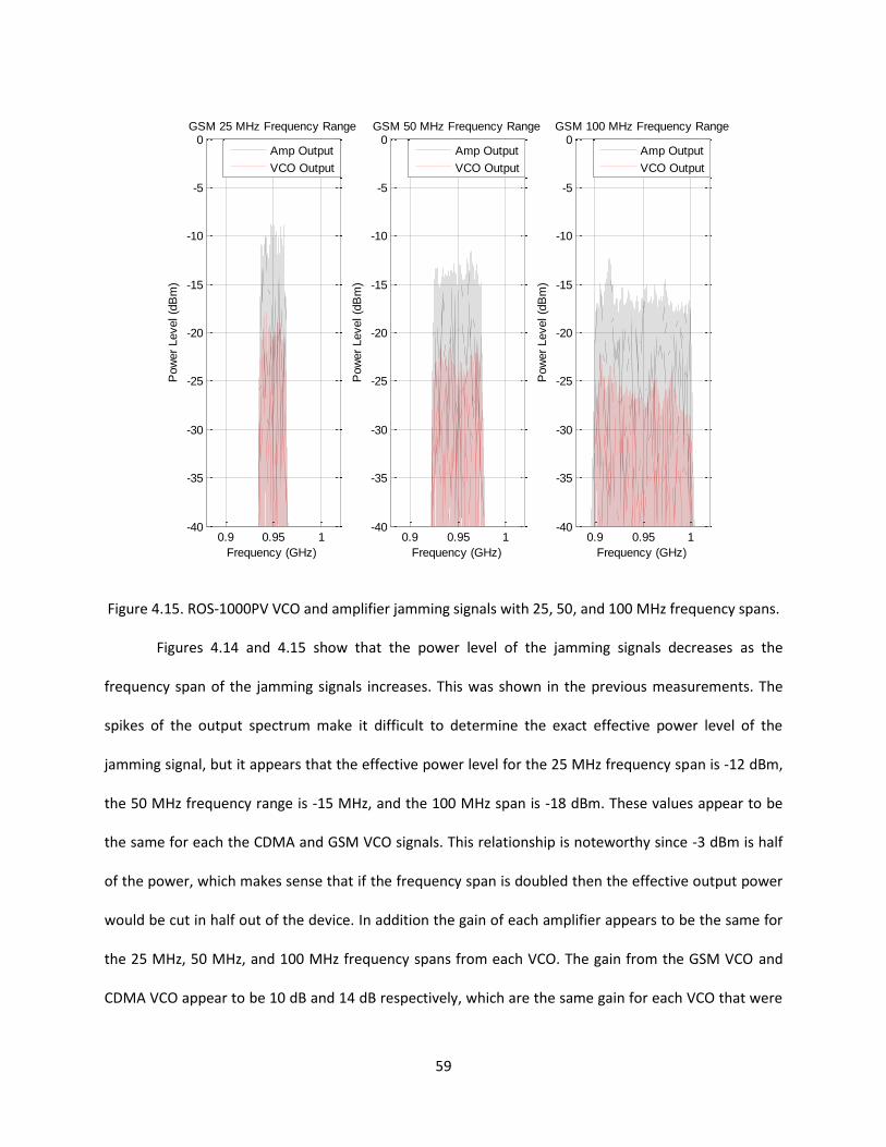
59
Figure 4.15. ROS-1000PV VCO and amplifier jamming signals with 25, 50, and 100 MHz frequency spans.
Figures 4.14 and 4.15 show that the power level of the jamming signals decreases as the
frequency span of the jamming signals increases. This was shown in the previous measurements. The
spikes of the output spectrum make it difficult to determine the exact effective power level of the
jamming signal, but it appears that the effective power level for the 25 MHz frequency span is -12 dBm,
the 50 MHz frequency range is -15 MHz, and the 100 MHz span is -18 dBm. These values appear to be
the same for each the CDMA and GSM VCO signals. This relationship is noteworthy since -3 dBm is half
of the power, which makes sense that if the frequency span is doubled then the effective output power
would be cut in half out of the device. In addition the gain of each amplifier appears to be the same for
the 25 MHz, 50 MHz, and 100 MHz frequency spans from each VCO. The gain from the GSM VCO and
CDMA VCO appear to be 10 dB and 14 dB respectively, which are the same gain for each VCO that were
0.9 0.95 1-40
-35
-30
-25
-20
-15
-10
-5
0GSM 25 MHz Frequency Range
Frequency (GHz)
Pow
er
Level (d
Bm
)
Amp Output
VCO Output
0.9 0.95 1-40
-35
-30
-25
-20
-15
-10
-5
0GSM 50 MHz Frequency Range
Frequency (GHz)
Pow
er
Level (d
Bm
)
Amp Output
VCO Output
0.9 0.95 1-40
-35
-30
-25
-20
-15
-10
-5
0GSM 100 MHz Frequency Range
Frequency (GHz)P
ow
er
Level (d
Bm
)
Amp Output
VCO Output

60
in the previous measurements. Since the 3 dB drop in power was visually determined, the mean and
standard deviation of the power levels were plotted in Figure 4.16 to verify.
Figure 4.16. Mean and standard deviation of power levels of the jamming signals that span 25, 50, and 100 MHz.
Figure 4.16 shows that both the GSM and CDMA jamming signals decrease at approximately the
same rate with the increased frequency range of the jamming signal. It can also be seen that the -3 dB
drop when the frequency range is doubled is also consistent in the mean power level and the high end
of the standard deviation. The power level drop of the CDMA jamming signal from the 25 MHz span to
the 50 MHz span appears to be slightly less than 3 dB, but this can be due to the frequency range not
being exactly 25 and 50 MHz. The high end of the power level range is also less than that from the visual
interpretation, which also occurred in the other calculations of the mean and standard deviation of the
jamming signal.
Even though it appears that the power levels decrease with the increase of the span at the
same rate, there will be a point at which the change in voltage of the triangular wave is too steep for the
20 30 40 50 60 70 80 90 100 110-32
-30
-28
-26
-24
-22
-20
-18
-16
-14Power Level Mean and Standard Deviation of Different Frequency Ranges
Pow
er
Level (d
Bm
)
Frequency Range (MHz)
GSM
CDMA

61
frequency of the triangular wave. It was determined from Figure 4.6(a) that the uniformity of the
jamming signal becomes poor if the frequency of the triangular wave is too fast. In actuality it has more
to do with the slope (or slew rate) of the triangular wave in V/us. For the GSM signal at 2 MHz, the slew
rate would be 4 V/us. For comparison, slew rate of the 100 kHz triangular wave that the GSM VCO while
producing the 100 MHz wide jamming signal is approximately .6 V/us since the peak to peak voltage is
approximately 3V and half of the period is 5 us. The maximum slew rate that can be used in each
triangular wave will depend on the VCO that is chosen, but the jamming signal out of the VCO will start
to lose uniformity at a certain point as the slew rate of the triangular wave increases.
4.4 Transmission of the Jamming Signal
The previous section examined the CDMA and GSM barrage jamming signals and how the
variables were used in creating them. After the jamming signals leave the amplifier, the signal is fed to
the antenna to transmit the signal. This design was based on creating a jamming signal for a specific
communication standard so additional communication standards can be jammed if the threat arises by
simply duplicating the design with an appropriate VCO and amplifier. Since this design creates a
separate jamming signal for each communication standard that is desired to be jammed, an antenna is
required for each jamming signal.
In this work, the actual transmission measurements of the jamming signals were not made, but
an estimation of the jamming signal’s power level at the receiver can be made from Equation 4. If the
desired distance for the jammer to work is 10 m, then that would result in a free space path loss of
approximately 51.5 dB and 52 dB for the CDMA and GSM jamming signals respectively. Assuming the
jamming and receiver antennas have a loss of 3 dB, then the jamming signal’s power level at the
receiver would be approximately -74.5 dBm and -75 dBm for the CDMA and GSM jamming signal’s

62
respectively, using a power level leaving the amplifier of -17 dBm. The power level of -17 dBm was
chosen from high end of the power range of the mean and standard deviation plots. That would mean
that this design would be able to successfully jam a GSM900 or CDMA850 signal at a power level of -76
dBm. This is an estimation since the antenna transmission of these signals have not characterized. Also
since the design would most likely require multiple antennas, how the multiple antennas would react
with each other needs to be tested.
Since the two GSM900 and CDMA850 jamming signals would be transmitted at the same time,
measurements were made to see how the two signals would react to being combined together. Figure
4.17 shows the combination of the CDMA and GSM jamming signals after leaving the amplifiers.
Figure 4.17. CDMA and GSM jamming signal output from the power combiner.
It can be seen through visual inspection that the effective power level of both GSM and CDMA
jamming signals are approximately -20 dBm. This means that there was a loss of 5 dB for each signal
through the lowpass filters and combiner since the visual inspection of the original jamming signals were
0.8 0.82 0.84 0.86 0.88 0.9 0.92 0.94 0.96 0.98 1-60
-50
-40
-30
-20
-10
0GSM and CDMA Output of Combiner
Frequency (GHz)
Pow
er
Level (d
Bm
)

63
at -15 dBm. The mean and standard deviation of these power signals were not calculated, but the visual
5 dB loss will be subtracted from the -17 dBm taken from the previous high end of the power range in
the mean and standard deviation plots. Also after the combiner there are additional noise spectrums
below the CDMA spectrum and above the GSM spectrum approximately 15 dB below the CDMA and
GSM power level. This would mean that with the same assumptions, 10 meter jamming distance and
receiver loss of 3 dB, that both signals would be able to jam a signal of -81 dBm. This power drop
through the combiner is sufficient, but there is a chance of the loss due to multiple antennas being
greater. Additional ways to combine the signals with less loss should be examined to optimize the
combination of the two jamming signals.
Even though, through the calculations, the design is stated to jam CDMA850 and GSM900
signals with a power level of -81 dBm if the combiner is used; finding and testing antennas is needed
before the result can be verified.

64
Chapter 5
Conclusion and Future Work
This chapter will discuss the conclusions of the design along with potential work that needs to
be done or to improve upon the design.
5.1 Conclusions
The purpose of this paper was to determine how to create barrage jamming signals for specific
communication standards and what techniques should be used to optimize the jamming signal. Since
the barrage jamming technique requires the jamming signal to raise the noise floor of the receiver at a
specific frequency, noise must be modulated onto a carrier frequency to create the jamming signal. This
was accomplished by applying noise directly to the input of a voltage controlled oscillator, which in turn
modulated the noise onto a carrier frequency with a bandwidth that is related to the amplitude of the
noise at the tuning input of the VCO. It was determined that the entire available bandwidth in both the
CDMA850 and GSM900 downlink spectrums can successfully be created by applying a large amplitude of
noise directly to the tuning input of the VCO, although the uniformity of the jamming signal spectrum
will be poor. The ideal barrage jamming signal will have a frequency range spanning the communication
standards downlink frequency range with a uniform power level across the spectrum. Since applying
only noise to the tuning input of the VCO results in a poor uniformity across the spectrum, additional
measures had to be taken to improve the uniformity.
To improve on the uniformity of the jamming signals created by adding only noise to the VCO
tuning input, applying a smaller amount of noise to a triangular wave was done. This improved on the

65
uniformity of the jamming signal, but various tests were completed on the variables such as the
frequency of the triangular wave, amount of noise applied to the triangular wave, and the peak to peak
voltage of the triangular wave which would determine the frequency span of the jamming signal. The
frequency of the triangular wave must be high enough to ensure that the jamming signal covers the
frequency of the communication signal enough to raise the bit error rate enough to disrupt the signal.
The frequency of the triangular wave will also have some effect on the jamming signal itself. From the
measurements in Section 4.3.1, it was seen that the jamming signal was similar for a triangular wave
frequency of 500, 300, 200, and 100 kHz. When the frequency was tested at 2 MHz, the uniformity
became worse. This appeared to be caused by the slew rate of the triangular wave being too high for
the VCO which caused peaks and valleys throughout the spectrum. There will be a slew rate for each
VCO that will cause it to lose uniformity and that should be tested upon a design of a new band with a
new VCO.
Other than the frequency of the triangular wave, the amount of noise being swept by the
triangular wave was also tested in Section 4.3.2. This showed that a 10, 5, and 2.5 MHz bandwidth of
noise swept by a triangular wave of the same frequency had little effect on the uniformity or power
level of the jamming signal. It should be noted that these bandwidths of noise were less than a quarter
of the entire frequency range of the jamming signal, so using a bandwidth of noise much closer to the
frequency span of the jamming signal may still need to be tested.
Lastly the frequency range that the triangular wave covers was tested to determine how the
output spectrum of the jamming signal reacts to a larger frequency range in Section 4.3.4. This shows
that as the frequency range is increased the power level of the jamming signal decreases. It is hard to
determine the exact level of the power signal due to random spikes cause by the noise, but it can be
estimated that doubling the frequency span of the jamming signal will cause the power level to decrease
by 3 dB. For the VCOs used to test the design, the increased frequency range did not affect the
66
uniformity of the jamming signal, but there could be a peak to peak voltage at a triangular wave
frequency that would have a slew rate too large for the VCO and cause uniformity issues in the jamming
signal.
Overall the jamming signals were successfully created by the use of a bandwidth of noise
applied to a triangular wave at the tuning input of the VCO. Although by doing this, the output power
level of the spectrum is drastically decreased. The output power of the jamming signal leaving the
amplifier also drastically decreases as the bandwidth increases to cover the entire spectrum. The stated
output power of the amplifier used in this design is +22 dBm, but the measured jamming signals at a
bandwidth of around 50 MHz had a power level of -17 dBm. That is a power loss of 39 dB which is
extremely significant. While it cannot be assumed that other amplifiers will have a power loss of 39 dB,
amplifying a large bandwidth of noise will cause the power level to be much less than if the amplifier
was amplifying a single frequency.
5.2 Future Work
While this paper covered the creation and optimization of a barrage jamming signal, additional
work can be done. The first area of work that should be accomplished is determining how the
transmission of the jamming signal will be affected by the antenna. Since antennas are usually used to
transmit signals with a much smaller bandwidth than the jamming signal, it should be determined how
an antenna reacts to the large bandwidth of the jamming signal. Also since the design uses one antenna
per jamming signal, testing should be done to determine the negative effects of using multiple antennas
near each other.
Along with the antenna testing, it is possible to upgrade the way in which the triangular wave is
produced. The current design uses a 555 timer which requires passive components to dictate the

67
frequency and peak to peak voltage of the triangular wave. It would be possible to create the jamming
signal using a digital to analog converter (DAC) so long as the individual DAC has the ability to create the
desired triangular wave. By using a DAC to create the triangular wave, the frequency span of the
jamming signal could be changed by the user to widen or narrow the spectrum. This would also require
a microcontroller to interact with the DAC, but it would be possible to create a jamming signal to span
any frequency that the VCO can produce.
The way in which the jamming signals can be combined should also be examined in the future
work. Since the combiner circuit used for the GSM900 and CDMA850 jamming signals show a loss of
approximately 5 dB, additional combination techniques should be examined. One of these ways would
be to offset the transmission of the jamming signals in a time delay fashion. This would allow for only a
single jamming signal to transmit at one time while using the same antenna for both jamming signals. If
a time delay transmission was used, the bit error rate calculations must be redone to make sure the
jamming signals would still be effective.
Another portion of the future work could be designing the components (VCO and amplifier)
specifically for this application. All of the parts in this design are commercially available and are designed
to have specific properties such as the phase noise. Since our design does not require the VCO and
amplifier to care about phase noise, a VCO or amplifier could be designed with more desirable specs for
this application, such as efficiency and output power.

68
References
[1] D. Adamy, EW101 A First Course in Electronic Warfare, Norwood, MA: ARTECH HOUSE, 2001.
[2] A. D. Martino, Introduction to Modern EW Systems, Boston: ARTECH HOUSE, 2012.
[3] FCC, "FCC Jammer Enforcement," [Online]. Available: http://www.fcc.gov/encyclopedia/jammer-
enforcement. [Accessed 1 April 2015].
[4] B. Razavi, RF Microelectronics Second Edition, Upper Saddle River, NJ: Prentice Hall, 2012.
[5] I. Poole, "GSM EDGE Tutorial," [Online]. Available: http://www.radio-
electronics.com/info/cellulartelecomms/gsm-edge/basics-tutorial-technology.php. [Accessed 19
October 2014].
[6] I. Leon W. Couch, Digital and Analog Communication Systems Seventh Edition, Upper Saddle River,
NJ: Prentice Hall, 2007.
[7] I. Poole, "Free Space Path Loss: Details, Formula, Calculator," [Online]. Available:
http://www.radio-electronics.com/info/propagation/path-loss/free-space-formula-equation.php.
[Accessed 16 November 2014].
[8] C. K. Alexander, Fundamentals of Electric Circuits, New York, NY: McGraw-Hill Companies, 2009.
[9] Mini-Circuits, "ROS-892-119+," M107895 EDR-8082A datasheet, 2013.
[10] Mini-Circuits, "ROS-1000PV," M102713 ED-6448A/1 datasheet, 2013.
[11] M. Dennis, "Circuit Notebook," 7th January 2005. [Online]. Available:
http://archive.siliconchip.com.au/cms/A_103659/article.html. [Accessed 9th December 2014].
[12] Texas Instruments, "TLC555 LinCMOS TIMER," SLFS043F datasheet Sept. 1983 [Revised Feb. 2005].
[13] "Panasonic NCR18650B Protected 3400mAh," [Online]. Available: http://lygte-
info.dk/review/batteries2012/Panasonic%20NCR18650B%20Protected%203400mAh%20%28Green
%29%20UK.html. [Accessed 26 November 2014].