design, fabrication and testing of a capacitive sensor
TRANSCRIPT
UNLV Theses, Dissertations, Professional Papers, and Capstones
5-1-2017
Design, Fabrication and Testing of a CapacitiveSensor Using Delta-Sigma ModulationCharikleia TsagkariUniversity of Nevada, Las Vegas, [email protected]
Follow this and additional works at: https://digitalscholarship.unlv.edu/thesesdissertations
Part of the Electrical and Computer Engineering Commons
This Thesis is brought to you for free and open access by Digital Scholarship@UNLV. It has been accepted for inclusion in UNLV Theses, Dissertations,Professional Papers, and Capstones by an authorized administrator of Digital Scholarship@UNLV. For more information, please [email protected].
Repository CitationTsagkari, Charikleia, "Design, Fabrication and Testing of a Capacitive Sensor Using Delta-Sigma Modulation" (2017). UNLV Theses,Dissertations, Professional Papers, and Capstones. 3049.https://digitalscholarship.unlv.edu/thesesdissertations/3049

DESIGN, FABRICATION AND TESTING OF A CAPACITIVE SENSOR USING DELTA-
SIGMA MODULATION
By
Charikleia Tsagkari
Bachelor of Science in Electrical and Computer Engineering
National Technical University of Athens
2009
A thesis submitted in partial fulfillment
of the requirements for the
Master of Science in Engineering – Electrical Engineering
Department of Electrical and Computer Engineering
Howard R. Hughes College of Engineering
The Graduate College
University of Nevada, Las Vegas
May 2017

Copyright 2017 by Charikleia Tsagkari
All Rights Reserved

ii
Thesis Approval
The Graduate College The University of Nevada, Las Vegas
May 1, 2017
This thesis prepared by
Charikleia Tsagkari
entitled
DESIGN, FABRICATION AND TESTING OF A CAPACITIVE SENSOR USING DELTA-SIGMA MODULATION
is approved in partial fulfillment of the requirements for the degree of
Master of Science in Engineering – Electrical Engineering Department of Electrical and Computer Engineering
R. Jacob Baker, Ph.D. Kathryn Hausbeck Korgan, Ph.D. Examination Committee Chair Graduate College Interim Dean Peter Stubberud, Ph.D. Examination Committee Member Yahia Baghzouz, Ph.D. Examination Committee Member Evangelos Yfantis, Ph.D. Graduate College Faculty Representative
iii
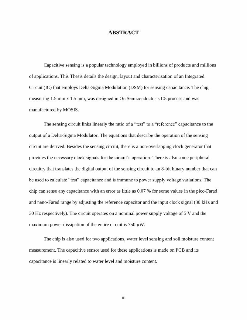
ABSTRACT
Capacitive sensing is a popular technology employed in billions of products and millions
of applications. This Thesis details the design, layout and characterization of an Integrated
Circuit (IC) that employs Delta-Sigma Modulation (DSM) for sensing capacitance. The chip,
measuring 1.5 mm x 1.5 mm, was designed in On Semiconductor’s C5 process and was
manufactured by MOSIS.
The sensing circuit links linearly the ratio of a “test” to a “reference” capacitance to the
output of a Delta-Sigma Modulator. The equations that describe the operation of the sensing
circuit are derived. Besides the sensing circuit, there is a non-overlapping clock generator that
provides the necessary clock signals for the circuit’s operation. There is also some peripheral
circuitry that translates the digital output of the sensing circuit to an 8-bit binary number that can
be used to calculate “test” capacitance and is immune to power supply voltage variations. The
chip can sense any capacitance with an error as little as 0.07 % for some values in the pico-Farad
and nano-Farad range by adjusting the reference capacitor and the input clock signal (30 kHz and
30 Hz respectively). The circuit operates on a nominal power supply voltage of 5 V and the
maximum power dissipation of the entire circuit is 750 μW.
The chip is also used for two applications, water level sensing and soil moisture content
measurement. The capacitive sensor used for these applications is made on PCB and its
capacitance is linearly related to water level and moisture content.

iv
ACKNOWLEDGEMENTS
I would like to express my sincere gratitude and respect to my advisor Dr. R Jacob Baker,
whose extensive knowledge, wise guidance and continued support helped me during my studies
at UNLV. I greatly appreciate his contribution of time, ideas, and funding that made my MS
degree a very productive and fulfilling experience. I am especially grateful for the excellent
example he has provided me as a successful professional and a great professor.
I would also like to thank the members of my thesis committee, Dr Peter Stubberud, Dr
Yahia Baghzouz and Dr Evangelos Yfantis, for their encouragement and genuine support
throughout my studies.
v
For my husband, Kostas and my daughter, Fey.
My strength, my inspiration, my life.
Thank you.

vi
TABLE OF CONTENTS
ABSTRACT ................................................................................................................................... iii
ACKNOWLEDGEMENTS ........................................................................................................... iv
TABLE OF CONTENTS ............................................................................................................... vi
LIST OF TABLES ......................................................................................................................... ix
LIST OF FIGURES ........................................................................................................................ x
CHAPTER 1: INTRODUCTION ................................................................................................... 1
CHAPTER 2: CIRCUIT DESIGN AND LAYOUT ...................................................................... 3
2.1 THE SENSING CIRCUIT .................................................................................................... 3
2.1.1 CLOCKED COMPARATOR OR SENSE AMPLIFIER .............................................. 5
2.1.2 SWITCHED-CAPACITOR CIRCUITS ...................................................................... 10
2.1.3 THE EQUATIONS FOR DELTA-SIGMA SENSING ............................................... 11
2.1.4 INCOMPLETE SETTLING ........................................................................................ 13
2.2 THE CLOCK GENERATOR ............................................................................................. 15
2.3 PERIPHERAL CIRCUITRY .............................................................................................. 17
2.3.1 THE D-FF .................................................................................................................... 19
2.3.2 THE COUNTER .......................................................................................................... 22
2.3.3 THE DAC .................................................................................................................... 23
vii
CHAPTER 3: THE CHIP ............................................................................................................. 27
CHAPTER 4: SIMULATIONS .................................................................................................... 31
4.1 SIMULATING THE ENTIRE CIRCUIT ........................................................................... 31
4.2 SIMULATING THE SENSING CIRCUIT (WITHOUT PERIPHERAL CIRCUITRY) .. 34
4.3 SENSING LARGER CAPACITORS ................................................................................. 36
4.4 POWER DISSIPATION ..................................................................................................... 39
4.5 POWER SUPPLY VOLTAGE (VDD) VARIATIONS ..................................................... 41
CHAPTER 5: TEST RESULTS ................................................................................................... 44
5.1 CAPACITORS IN THE pF RANGE .................................................................................. 45
5.2 CAPACITORS IN THE nF RANGE .................................................................................. 47
5.3 POWER DISSIPATION ..................................................................................................... 49
5.4 POWER SUPPLY VOLTAGE (VDD) VARIATIONS ..................................................... 50
CHAPTER 6: DESIGN DISCUSSION ........................................................................................ 52
6.1 VOLTAGE AT THE “BUCKET” CAPACITOR (VBUCKET) ............................................. 52
6.2 COMPARATOR ................................................................................................................. 53
6.3 SWITCHED CAPACITORS .............................................................................................. 53
6.4 INPUT CLOCK SIGNAL................................................................................................... 54
6.5 COUNTER .......................................................................................................................... 55
6.6 POWER DISSIPATION ..................................................................................................... 55
CHAPTER 7: APPLICATIONS ................................................................................................... 58
viii
7.1 CAPACITIVE WATER LEVEL SENSOR........................................................................ 59
7.2 CAPACITIVE SOIL MOISTURE SENSOR ..................................................................... 61
7.3 APPLICATIONS DISCUSSION........................................................................................ 63
CHAPTER 8: CONCLUSION ..................................................................................................... 65
APPENDIX − SCHEMATICS AND LAYOUTS ........................................................................ 67
REFERENCES ............................................................................................................................. 73
CURRICULUM VITAE ............................................................................................................... 75

ix
LIST OF TABLES
Table 1 – Parametric analysis results for CTEST varying from 10 pF to 500 pF............................ 32
Table 2 – Parametric analysis results for CTEST varying from 500 pF to 1 nF.............................. 33
Table 3 − Parametric analysis results for CTEST varying from 10 nF to 500 nF ........................... 36
Table 4 − Parametric analysis results for CTEST varying from 500 nF to 1 μF ............................. 38
Table 5 − Simulation results for various VDDs............................................................................ 42
Table 6 − Test results for capacitors in the pF range .................................................................... 46
Table 7 − Test results for capacitors in the nF range .................................................................... 48
Table 8 − Test results for power dissipation ................................................................................. 49
Table 9 – Test results for power supply voltage (VDD) variations .............................................. 50
Table 10 − Test results for capacitive water level sensing application......................................... 60
Table 11 − Test results for capacitive soil moisture sensing application ..................................... 62
x
LIST OF FIGURES
Figure 1 − Block diagram of a 1st order Delta-Sigma Modulator ................................................... 3
Figure 2 – Schematic of the sensing circuit .................................................................................... 4
Figure 3 − The output of the comparator and the voltages at CREF, CBUCKET and CTEST ................ 5
Figure 4 − The clocked comparator ................................................................................................ 6
Figure 5 Kickback noise for Inp (blue) and Inm (red) ................................................................. 7
Figure 6 The current that flows in the sense amplifier ................................................................ 7
Figure 7 The offset of the comparator ......................................................................................... 8
Figure 8 The design of the comparator in Cadence ..................................................................... 9
Figure 9 Layout of the comparator .............................................................................................. 9
Figure 10 − Switched-capacitor resistor ....................................................................................... 10
Figure 11 − Sensing circuit with SC resistors ............................................................................... 11
Figure 12 − The voltage at CREF for clock frequency f = 33 kHz ................................................. 14
Figure 13 − The voltage at CREF for clock frequency f = 250kHz ................................................ 14
Figure 14 − The voltage at CREF for clock frequency f = 250kHz and wider devices .................. 15
Figure 15 − Non-overlapping clock signals .................................................................................. 16
Figure 16 − Schematic of the clock generator .............................................................................. 16
Figure 17 − Schematic of the clock generator in Cadence ........................................................... 17
Figure 18 − Layout of the clock generator.................................................................................... 17
Figure 19 − Peripheral circuitry .................................................................................................... 18
Figure 20 − Edge-triggered D flip-flop ......................................................................................... 19

xi
Figure 21 − Schematic of the D-FF in Cadence ........................................................................... 20
Figure 22 − Layout of the D-FF in Cadence ................................................................................. 20
Figure 23 − Schematic of the edge-triggered D-FF with clear ..................................................... 21
Figure 24 − Schematic of the edge-triggered D-FF with clear in Cadence .................................. 21
Figure 25 − Layout of the edge-triggered D-FF with clear in Cadence........................................ 21
Figure 26 − Schematic of the 8-bit asynchronous counter ........................................................... 22
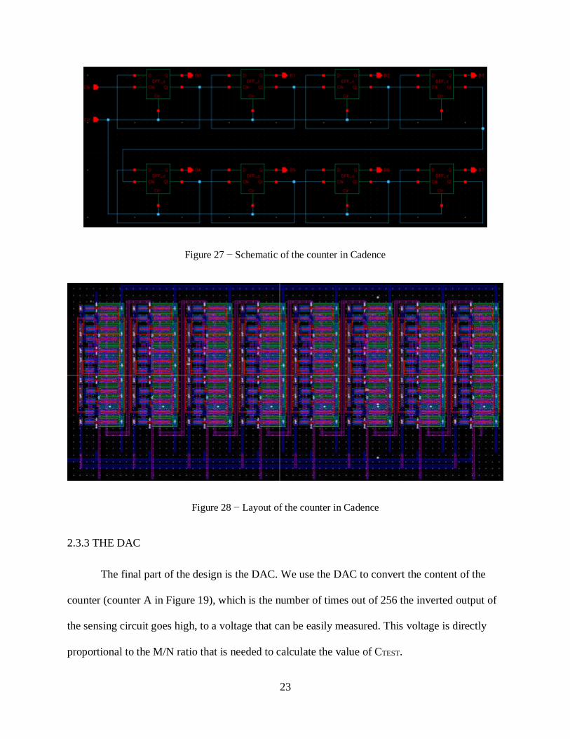
Figure 27 − Schematic of the counter in Cadence ........................................................................ 23
Figure 28 − Layout of the counter in Cadence ............................................................................. 23
Figure 29 − Schematic of the 8-bit DAC ...................................................................................... 24
Figure 30 − Schematic of the 8-bit DAC in Cadence ................................................................... 26
Figure 31 − Layout of the 8-bit DAC in Cadence ........................................................................ 26
Figure 32 − Schematic of the chip with the bonding pads ............................................................ 27
Figure 33 − The bonding diagram of the chip .............................................................................. 28
Figure 34 − Layout of the chip in Cadence................................................................................... 29
Figure 35 − Photograph of the chip .............................................................................................. 30
Figure 36 − The schematic of the circuit used for the simulations drawn in Cadence ................. 31
Figure 37 − Simulation results for CTEST varying from 10 pF to 500 pF ...................................... 32
Figure 38 − Simulation results for CTEST varying from 500 pF to 1 nF ........................................ 33
Figure 39 − The schematic used to simulate the sensing circuit without the peripheral circuitry 34
Figure 40 − Simulating the sensing circuit for CTEST varying from 50 pF to 500 pF ................... 35
Figure 41 − Simulating the sensing circuit for CTEST varying from 500 pF to 1 nF ..................... 35
Figure 42 − Simulation results for CTEST varying from 10 nF to 500 nF ...................................... 37
Figure 43 − Simulating the sensing circuit for CTEST varying from 50 nF to 500 nF ................... 37
xii
Figure 44 − Simulation results for CTEST varying from 500 nF to 1 μF ....................................... 38
Figure 45 − Simulating the sensing circuit for CTEST varying from 500 nF to 1 μF ..................... 39
Figure 46 − Power dissipation (in μW) for different capacitor values (10 pF-500 pF) ................ 40
Figure 47 − Power dissipation (in μW) for different capacitor values (500 pF-1 nF) .................. 41
Figure 48 − Simulating the circuit for different values of VDD................................................... 43
Figure 49 − Test setup for the fabricated chip .............................................................................. 44
Figure 50 − Graphical representation of test results for capacitors in the pF range ..................... 47
Figure 51 − Graphical representation of the test results for capacitors in the nF range ............... 48
Figure 52 − Test results for power dissipation.............................................................................. 49
Figure 53 − Power supply voltage (VDD) variations for the output of the sensing circuit (Outi) 51
Figure 54 − Power supply voltage (VDD) variations for the output of the DAC (Output_DAC) 51
Figure 55 − Two different types of capacitor configurations ....................................................... 58
Figure 56 − The capacitive sensor ................................................................................................ 58
Figure 57 − The sensor as designed in Eagle [11] ........................................................................ 59
Figure 58 − Test setup for capacitive water level sensing ............................................................ 59
Figure 59 − Test results for capacitive water level sensing application ....................................... 60
Figure 60 −Test setup for capacitive soil moisture sensing .......................................................... 61
Figure 61 − Test results for capacitive soil moisture sensing application .................................... 63
1
CHAPTER 1: INTRODUCTION
Capacitive sensing is a popular technology employed in billions of products and millions
of applications such as cell phone and laptop displays, biomedicine, robotics, fingerprinting,
automotive, etc. This versatile sensor category offers higher precision and robustness, simpler
construction and lower power than resistive-based alternatives [1]. In the center of this
development is the sensing method itself, the process by which the capacitance is being
measured and converted into digital words that can be processed, manipulated and interpreted. A
few of the most commonly used sensing methods are Charge Transfer, Successive
Approximation, Mutual Capacitance Measurement and Delta-Sigma Modulation [2]. Great effort
is being put to maximize sensitivity, accuracy, and responsiveness of the sensors while
minimizing power dissipation.
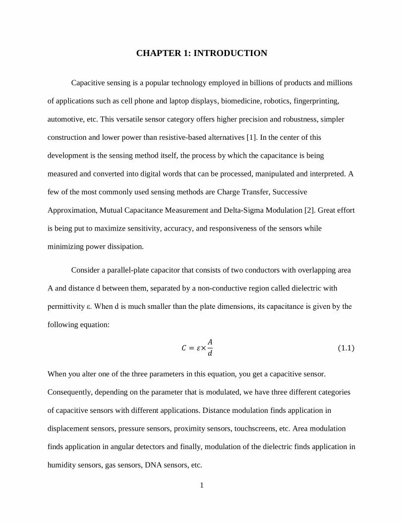
Consider a parallel-plate capacitor that consists of two conductors with overlapping area
A and distance d between them, separated by a non-conductive region called dielectric with
permittivity ε. When d is much smaller than the plate dimensions, its capacitance is given by the
following equation:
𝐶 = 𝜀×𝐴
𝑑 (1.1)
When you alter one of the three parameters in this equation, you get a capacitive sensor.
Consequently, depending on the parameter that is modulated, we have three different categories
of capacitive sensors with different applications. Distance modulation finds application in
displacement sensors, pressure sensors, proximity sensors, touchscreens, etc. Area modulation
finds application in angular detectors and finally, modulation of the dielectric finds application in
humidity sensors, gas sensors, DNA sensors, etc.
2
The development of the read-out or sensing circuitry for this kind of sensors is however a
great challenge as generally a very small signal has to be detected in an extremely noisy
environment [3]. A powerful and practical circuit technique called Delta-Sigma (ΔΣ) modulation
(also known as Sigma-Delta (ΣΔ) modulation) is ideal for sensing applications where the desired
signal we are sensing is a constant but may be corrupted with noise [4,5].
Until recently designers have been forced to convert variance in capacitance to a variance
in voltage, current, frequency or pulse width, which is then converted to digital using an Analog-
to-Digital Converter (ADC) employing Delta-Sigma modulation [6,7]. The design proposed in
this thesis permits direct interfacing between the capacitive sensor and the Delta-Sigma ADC,
which brings inherent features such as high resolution, accuracy, and linearity. The output data
represent the ratio between the capacitive sensor (CTEST) and a reference capacitor (CREF), both
off-chip.
This thesis presents the design, layout, simulation and testing of a capacitive sensing
circuit using Delta-Sigma Modulation (DSM). Chapter 2 demonstrates the circuit’s design and
layout that were designed using Cadence Virtuoso software and explains the operation of the
circuit. Chapter 3 offers details about the chip that was manufactured by MOSIS in ON
Semiconductor’s C5 process [8]. Chapter 4 shows the circuit’s simulation results, whereas
Chapter 5 details the chip’s testing results. Chapter 6 presents some design considerations that
resulted from simulating and then testing the operation of the circuit. Chapter 7 showcases two
possible applications of the chip. Finally, Chapter 8 is the conclusion of this thesis.
3
CHAPTER 2: CIRCUIT DESIGN AND LAYOUT
2.1 THE SENSING CIRCUIT
The sensing circuit consists of an analog-to-digital converter (ADC) employing Delta-
Sigma Modulation (DSM). In a conventional ADC, the analog input signal is sampled with a
sampling frequency and then quantized into a digital signal. This process adds noise to the input
signal, also known as quantization noise. In a Delta-Sigma Modulator, a type of Noise-Shaping
modulator, feedback is used to improve the overall data conversion performance. The digital
output of the ADC passes through a digital-to-analog converter (DAC), then it is subtracted
(Delta) from the input signal and finally the integrator sums (Sigma) this difference and feeds it
forward to the ADC. This forces the output of the modulator to follow the average of the input
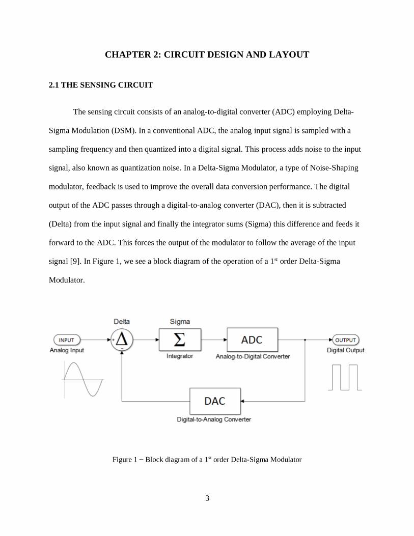
signal [9]. In Figure 1, we see a block diagram of the operation of a 1st order Delta-Sigma
Modulator.
Figure 1 − Block diagram of a 1st order Delta-Sigma Modulator

4
Figure 2 shows the sensing circuit of the chip. The capacitor CBUCKET acts as an integrator
(Sigma), the clocked comparator is the 1-bit ADC and the 1-bit DAC is the feedback from the
output back into the positive terminal of the comparator through a PMOS (P2).
Figure 2 – Schematic of the sensing circuit
CBUCKET is constantly being discharged through the bottom switched-capacitor (SC)
resistor while the feedback is trying to keep the voltage across the capacitor to the reference
voltage. When the output of the comparator is low, in other words when the voltage across
CBUCKET is less that the reference voltage VREF (VREF = VDD/2 = 2.5 V from the voltage divider),
P2 turns on and CBUCKET charges through the upper SC resistor. When the output of the
comparator goes high (5 V for C5 process), P2 turns off and CBUCKET discharges through the
bottom switched-capacitor (see Figure 3). All three capacitors are off-chip.

5
Figure 3 − The output of the comparator and the voltages at CREF, CBUCKET and CTEST
2.1.1 CLOCKED COMPARATOR OR SENSE AMPLIFIER
The comparator, or sense amplifier, is a 1-bit analog-to-digital converter. It takes 2
analog inputs, calculates their difference and if the difference is positive then the output of the
comparator is a logic high, otherwise the output is a logic low. In our case, the comparator
compares the voltage across CBUCKET (positive terminal) and the reference voltage (negative
terminal) which is at VDD/2. It is a clocked comparator and it is designed so that the output
changes only on the rising edge of the clock.
In Figure 4, we see the schematic of the clocked comparator with the SR latch and the
inverters. Although there are numerous options, this comparator design is simple, low power and
it works very well for small signal differences. The design is based on cross-coupled inverters
with added circuitry so that no static current flows into the circuit, all nodes are driven to known

6
voltages as long as the inputs are above the threshold voltage and to avoid clock feedthrough and
kickback noise.
Figure 4 − The clocked comparator
Clock feedthrough noise is present when a clock signal has a direct path to the inputs of
the sensing circuit. We minimize this noise by isolating the clock from inputs with 3 devices.
The kickback noise is present and injected into the inputs of the comparator when the latch
switches states [4]. We also minimize this noise by isolating the inputs from the high-swing
nodes. In Figure 5 we see the simulated kickback noise of the circuit. We drive the inputs to the
rails with inverters and the kickback noise is around 22 μV for the positive terminal and 2.4 mV
for the negative terminal of the comparator.
For minimum power dissipation and to avoid metastability issues, it is crucial to ensure
that there are no direct DC paths from VDD to ground except during switching times. In our

7
design, we use long L NMOS input devices so they never pull significant current [4]. In Figure 6
we see the simulated current that flows in the sense amplifier.
Figure 5 Kickback noise for Inp (blue) and Inm (red)
Figure 6 The current that flows in the sense amplifier
8
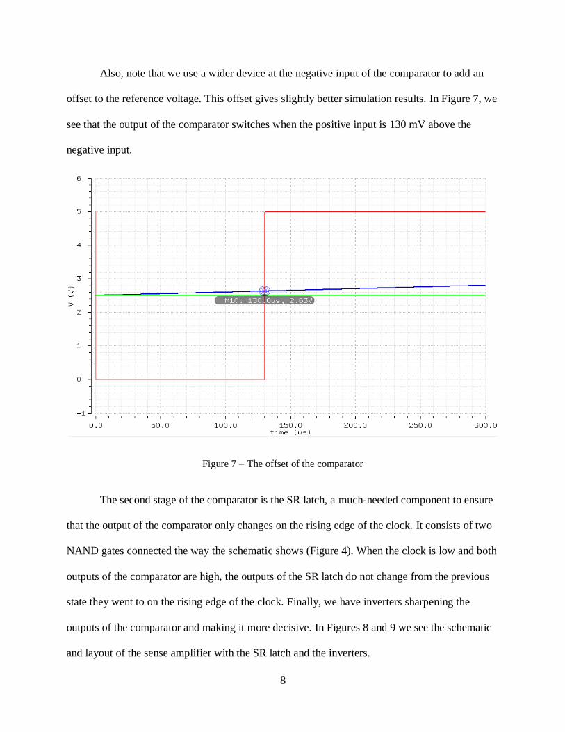
Also, note that we use a wider device at the negative input of the comparator to add an
offset to the reference voltage. This offset gives slightly better simulation results. In Figure 7, we
see that the output of the comparator switches when the positive input is 130 mV above the
negative input.
Figure 7 The offset of the comparator
The second stage of the comparator is the SR latch, a much-needed component to ensure
that the output of the comparator only changes on the rising edge of the clock. It consists of two
NAND gates connected the way the schematic shows (Figure 4). When the clock is low and both
outputs of the comparator are high, the outputs of the SR latch do not change from the previous
state they went to on the rising edge of the clock. Finally, we have inverters sharpening the
outputs of the comparator and making it more decisive. In Figures 8 and 9 we see the schematic
and layout of the sense amplifier with the SR latch and the inverters.

9
Figure 8 The design of the comparator in Cadence
Figure 9 Layout of the comparator

10
2.1.2 SWITCHED-CAPACITOR CIRCUITS
In this design, switched-capacitor (SC) resistors are used. Switched-capacitor circuits are
known to minimize power as long as they operate with non-overlapping clock signals. In Figure
10, there is a SC resistor with PMOS devices acting as switches. The two clock signals, φ1 and
φ2, are non-overlapping which means that they can never be low at the same time for PMOS
switches.
Figure 10 − Switched-capacitor resistor
When φ1 is low, the capacitor charges to V1 which is equal to 𝑄1 𝐶⁄ and when φ2 is low,
the capacitor charges to 𝑉2 = 𝑄2 𝐶⁄ [4]. The difference between Q1 and Q2 is transferred between
V1 and V2 during one clock cycle with period 𝑇 = 1 𝑓⁄ and it is given by
𝑄1 − 𝑄2 = 𝐶×(𝑉1 − 𝑉2) (2.1)
The average current is given by
𝐼 =𝐶×(𝑉1 − 𝑉2)
𝑇 (2.2)
And if we consider the resistance of the SC circuit as
𝑅𝑆𝐶 =𝑇
𝐶=
1
𝐶×𝑓 (2.3)
11
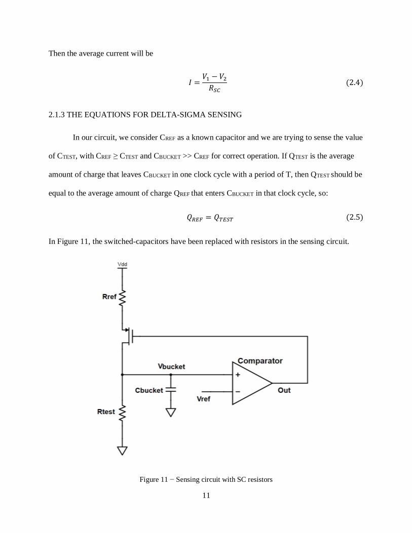
Then the average current will be
𝐼 =𝑉1 − 𝑉2
𝑅𝑆𝐶 (2.4)
2.1.3 THE EQUATIONS FOR DELTA-SIGMA SENSING
In our circuit, we consider CREF as a known capacitor and we are trying to sense the value
of CTEST, with CREF ≥ CTEST and CBUCKET >> CREF for correct operation. If QTEST is the average
amount of charge that leaves CBUCKET in one clock cycle with a period of T, then QTEST should be
equal to the average amount of charge QREF that enters CBUCKET in that clock cycle, so:
𝑄𝑅𝐸𝐹 = 𝑄𝑇𝐸𝑆𝑇 (2.5)
In Figure 11, the switched-capacitors have been replaced with resistors in the sensing circuit.
Figure 11 − Sensing circuit with SC resistors
12
Assuming a large open-loop gain, both inputs of the comparator are equal to VREF, so VBUCKET =
VREF. The average voltage across the top SC with a resistance of RREF, is VDD-VBUCKET and the
average current would be IREF:
𝐼𝑅𝐸𝐹 =𝑉𝐷𝐷 − 𝑉𝐵𝑈𝐶𝐾𝐸𝑇
𝑅𝑅𝐸𝐹=
𝑉𝐷𝐷 − 𝑉𝑅𝐸𝐹
𝑅𝑅𝐸𝐹 (2.6)
The average voltage across the bottom SC with a resistance of RTEST, is VREF and the average
current would be ITEST:
𝐼𝑇𝐸𝑆𝑇 =𝑉𝐵𝑈𝐶𝐾𝐸𝑇
𝑅𝑇𝐸𝑆𝑇 =
𝑉𝑅𝐸𝐹
𝑅𝑇𝐸𝑆𝑇 (2.7)
Let us assume that M is the number of clock cycles the comparator’s output goes low (or the
complimentary output 𝑂𝑢𝑡 ̅̅ ̅̅ ̅̅ goes high) and N is the total number of clock cycles [5]. Then the
average current that charges CBUCKET in one cycle would be IREF*(M/N) and by charge
conservation we get:
𝐼𝑇𝐸𝑆𝑇×𝑇 = 𝐼𝑅𝐸𝐹×𝑀
𝑁×𝑇 (2.8)
𝐼𝑇𝐸𝑆𝑇 = 𝐼𝑅𝐸𝐹×𝑀
𝑁 (2.9)
𝑉𝑅𝐸𝐹
𝑅𝑇𝐸𝑆𝑇=
𝑉𝐷𝐷 − 𝑉𝑅𝐸𝐹
𝑅𝑅𝐸𝐹×
𝑀
𝑁 (2.10)
𝑉𝐷𝐷
2×𝑅𝑇𝐸𝑆𝑇=
𝑉𝐷𝐷
2×𝑅𝑅𝐸𝐹×
𝑀
𝑁 (2.11)
𝑅𝑅𝐸𝐹
𝑅𝑇𝐸𝑆𝑇=
𝑀
𝑁 (2.12)
From switched-capacitor theory, we know that:
13
𝑅𝑆𝐶 =1
𝐶×𝑓 (2.13)
So now we get:
1𝐶𝑅𝐸𝐹×𝑓
1𝐶𝑇𝐸𝑆𝑇×𝑓
=𝑀
𝑁 (2.14)
𝐶𝑇𝐸𝑆𝑇 = 𝐶𝑅𝐸𝐹×𝑀
𝑁 (2.15)
Equation (2.15) shows the linear relationship between CTEST and CREF. Therefore, if we want to
sense the value of a capacitor, all we have to do is count how many times the positive output of
the comparator goes low (or the negative output goes high) and multiply this to the value of the
reference capacitor CREF.
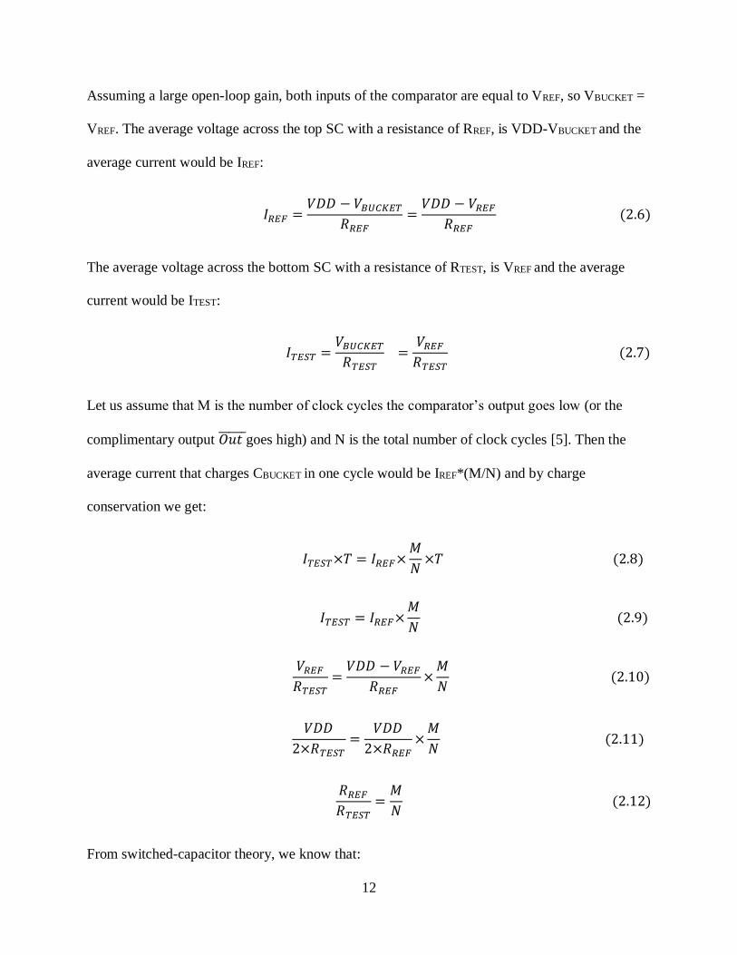
2.1.4 INCOMPLETE SETTLING
For the circuit’s proper operation, it is crucial that the voltage at the reference capacitor
CREF settles between the clock changes, in other words we must ensure that the CREF fully
charges and discharges within a clock cycle. Figure 12 shows the voltage at CREF (red dotted
line) for an input clock signal of 33 kHz (blue solid line). This voltage moves between 5 V and
2.5 V and it is clear that it settles completely before switching. The sensing circuit in this case
provides a correct result (CTEST = 250pF and the average output voltage is 2.5 V which means
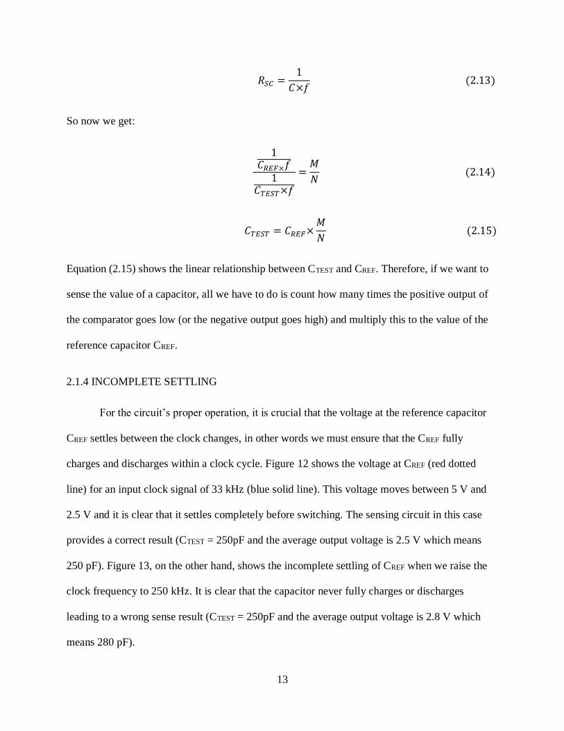
250 pF). Figure 13, on the other hand, shows the incomplete settling of CREF when we raise the
clock frequency to 250 kHz. It is clear that the capacitor never fully charges or discharges
leading to a wrong sense result (CTEST = 250pF and the average output voltage is 2.8 V which
means 280 pF).

14
Figure 12 − The voltage at CREF for clock frequency f = 33 kHz
Figure 13 − The voltage at CREF for clock frequency f = 250kHz

15
To eliminate the incomplete settling behavior, we can either lower the clock frequency or
use wider devices for the switched-capacitor. Figure 14 shows how the problem the higher
frequency (f = 250 kHz) created, is solved when we use wider devices for the SC circuit. In our
circuit, we choose to lower the clock frequency for lower power dissipation and smaller layout
area.
Figure 14 − The voltage at CREF for clock frequency f = 250kHz and wider devices
2.2 THE CLOCK GENERATOR
In a design that employs switched-capacitors, it is crucial to have non-overlapping clock
signals for correct operation. The rise and fall times of the clock signals should not occur at the
same time and there should be a period of dead time between transitions.
The schematic of the clock generator is shown in Figure 16. This circuit takes a clock
input and generates two non-overlapping clock signals. The delay through the NAND gate and

16
the two inverters after the NAND determine the amount of separation of the two signals [4]. The
additional inverters are used to buffer the outputs. Note that the 33 kHz phi1 and phi2 are used
for the NMOS devices (never high at the same times) and their compliments phi1b and phi2b are
used for the PMOS devices (never low at the same times) (see Figure 15).
Figure 15 − Non-overlapping clock signals
In Figure 17 and Figure 18 we see the schematic and layout of the clock generator in Cadence.
Figure 16 − Schematic of the clock generator

17
Figure 17 − Schematic of the clock generator in Cadence
Figure 18 − Layout of the clock generator
2.3 PERIPHERAL CIRCUITRY
Besides the sensing circuit and the clock generator, there is some additional circuitry that
is responsible for the presentation of the sensing circuit’s output. The output of the sensing
circuit is digital, a series of ones and zeros. An analog output would be more convenient and
easier to read. With the use of counters, logic gates, D flip-flops (D-FFs) and a DAC, we get an
analog output, a voltage that is proportional to the value of CTEST.

18
From Eq. (2.15), we know that in order to find the value of the capacitor we are sensing,
we need to count how many times the output of the sensing circuit goes low or the
complimentary output goes high. That is why we feed the complimentary output Outi to a
counter (counter A) and then to a DAC to get the analog output. The DAC has a resolution of 8
bits (𝑉𝐷𝐷 28⁄ = 5 256⁄ = 0.0195𝑉 = 19.5 𝑚𝑉). Every 256 clock cycles, the CLR (clear) signal
generated by counter B, a NAND and an inverter resets counter A. In Figure 19, there is a
diagram of the peripheral circuitry. The components enclosed by the dotted line generate the
CLR signal and the components enclosed by the red line generate the store signal.
Figure 19 − Peripheral circuitry

19
Since there is no need to see the change in the output of the DAC, we use D-FFs right
before the DAC to hold the final state of counter A (255 clock cycles) during the 256 clock
cycles. The D-FFs are clocked using the store signal generated by counter B, another NAND and
a NOR gate. The store signal goes high and changes the states of the D-FFs when counter B has
counted 255 clock cycles. Finally, the DAC outputs the analog signal. If you multiply this
voltage with the value of the reference capacitor CREF and divide it with the supply voltage VDD,
then you get the value of the capacitor we are trying to sense.
2.3.1 THE D-FF
In order to hold the final state of the counter, we use eight D-FFs before the DAC. These
are rising edge-triggered D-FFs which means that their output only changes on the rising edge of
the clock. We can make the D-FF change state on the falling edge of the clock by simply
switching the clock signals on the transmission gates (TGs). Figure 20 shows an implementation
of an edge-triggered D-FF. It consists of two latches, the master and the slave. When the clock is
low, the first stage tracks the D input and the second stage holds the previous state. When the
clock goes high, the first stage captures and transfers the input to the second stage [4]. In Figure
21 and 22, we see the schematic and layout of the edge-triggered D flip-flop.
Figure 20 − Edge-triggered D flip-flop

20
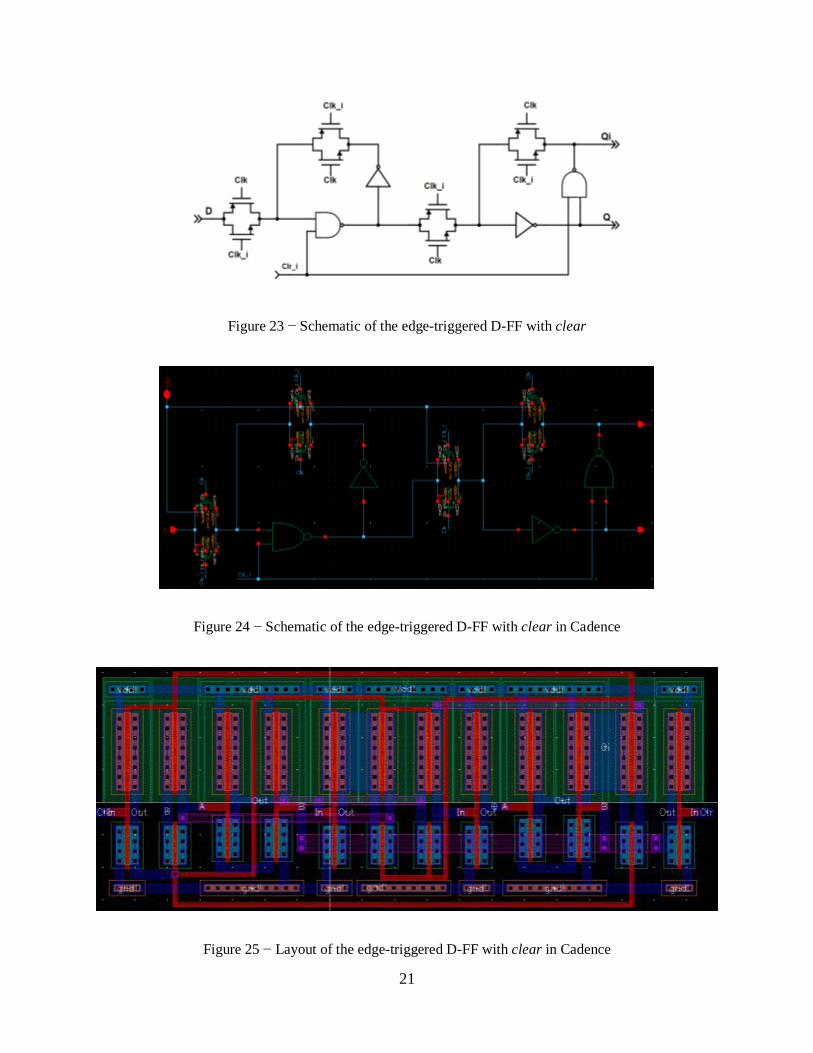
If we want to add the option of clearing the D-FF, we change two of the inverters with
NAND gates as shown in Figure 23. When Clr goes high (Clr_i goes low), the outputs of the
NAND gates go high and the outputs of the D-FF are forced to Q = 0 and Qi = 1. The schematic
and layout of the edge-triggered D-FF with clear option are shown in Figures 24 and 25.
Figure 21 − Schematic of the D-FF in Cadence
Figure 22 − Layout of the D-FF in Cadence
21
Figure 23 − Schematic of the edge-triggered D-FF with clear
Figure 24 − Schematic of the edge-triggered D-FF with clear in Cadence
Figure 25 − Layout of the edge-triggered D-FF with clear in Cadence
22
2.3.2 THE COUNTER
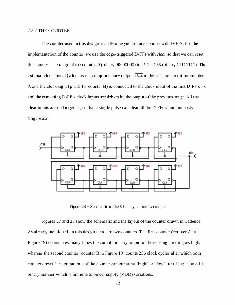
The counter used in this design is an 8-bit asynchronous counter with D-FFs. For the
implementation of the counter, we use the edge-triggered D-FFs with clear so that we can reset
the counter. The range of the count is 0 (binary 00000000) to 28-1 = 255 (binary 11111111). The
external clock signal (which is the complimentary output 𝑂𝑢𝑡̅̅ ̅̅ ̅ of the sensing circuit for counter
A and the clock signal phi1b for counter B) is connected to the clock input of the first D-FF only
and the remaining D-FF’s clock inputs are driven by the output of the previous stage. All the
clear inputs are tied together, so that a single pulse can clear all the D-FFs simultaneously
(Figure 26).
Figure 26 − Schematic of the 8-bit asynchronous counter
Figures 27 and 28 show the schematic and the layout of the counter drawn in Cadence.
As already mentioned, in this design there are two counters. The first counter (counter A in
Figure 19) counts how many times the complimentary output of the sensing circuit goes high,
whereas the second counter (counter B in Figure 19) counts 256 clock cycles after which both
counters reset. The output bits of the counter can either be “high” or “low”, resulting in an 8-bit
binary number which is immune to power supply (VDD) variations.
23
Figure 27 − Schematic of the counter in Cadence
Figure 28 − Layout of the counter in Cadence
2.3.3 THE DAC
The final part of the design is the DAC. We use the DAC to convert the content of the
counter (counter A in Figure 19), which is the number of times out of 256 the inverted output of
the sensing circuit goes high, to a voltage that can be easily measured. This voltage is directly
proportional to the M/N ratio that is needed to calculate the value of CTEST.
24
The DAC is implemented by an R-2R resistor ladder circuit, one of the simplest DAC
architectures, shown in Figure 29. The R–2R ladder operates as a string of current dividers,
whose output accuracy is solely dependent on how well each resistor is matched to the others.
The R-2R resistor ladder architecture is easy to design since only two resistor values are
required. It is fast and has fixed output impedance of R.
Figure 29 − Schematic of the 8-bit DAC
The digital inputs B0:B7 are switched between a logic high (VDD = 5 V) and a logic low
(GND = 0 V). Each input has a different contribution to the output voltage VOUT_DAC, which is
given by
𝑉𝑂𝑈𝑇_𝐷𝐴𝐶 = VDD×𝑉𝐷𝐼𝐺𝐼𝑇𝐴𝐿
2𝑛= 𝑉𝐷𝐷×
𝑀
𝑁 (2.16)
where n is the number of bits and
𝑉𝐷𝐼𝐺𝐼𝑇𝐴𝐿 = (𝐵0×20) + (𝐵1×21) + (𝐵2×22) + (𝐵3×23) + (𝐵4×24) + (𝐵5×25) + (𝐵6×26)
+ (𝐵7×27)
If, for example, all inputs are high then VOUT will be

25
𝑉𝑂𝑈𝑇𝑀𝐴𝑋 = 5×
(1×20) + (1×21) + (1×22) + (1×23) + (1×24) + (1×25) + (1×26) + (1×27)
28
= 5×255
256≈ 4.9805 𝑉 (2.17)
The minimum output voltage is 𝑉𝑂𝑈𝑇𝑀𝐼𝑁 = 0 𝑉 and the step with which the DAC’s output can
change (resolution) is
𝛥𝑉𝑂𝑈𝑇 = 5×1
256≈ 0.0195 𝑉 𝑜𝑟 19.5 𝑚𝑉 (2.18)
If we try to translate this into capacitor values and keeping in mind Eq. (2.15)
𝐶𝑇𝐸𝑆𝑇 = 𝐶𝑅𝐸𝐹×𝑀
𝑁
where M is the number of clock cycles the comparator’s complimentary output 𝑂𝑢𝑡 ̅̅ ̅̅ ̅̅ goes high
and N is the total number of clock cycles, the resolution of the 8-bit DAC is
𝐶𝑇𝐸𝑆𝑇 = 𝐶𝑅𝐸𝐹×1
28= 0.0039×𝐶𝑅𝐸𝐹 (2.19)
The largest error is for ½ LSB
𝐶𝑇𝐸𝑆𝑇 = 𝐶𝑅𝐸𝐹×0.5
28= 0.00195×𝐶𝑅𝐸𝐹 (2.20)
Consequently, if we want to keep the error under 2%, then
𝐶𝑇𝐸𝑆𝑇 =0.00195×𝐶𝑅𝐸𝐹
0.02= 0.0976×𝐶𝑅𝐸𝐹 ≈ 0.1×𝐶𝑅𝐸𝐹 (2.21)
In other words, if we want a good accuracy for the circuit, we must adjust CREF per the capacitor
we are sensing,
0.1×𝐶𝑅𝐸𝐹 ≤ 𝐶𝑇𝐸𝑆𝑇 ≤ 𝐶𝑅𝐸𝐹 (2.22)
26
For example, if the reference capacitor CREF = 500 pF, then we start getting more accurate results
(error less than 2%) for CTEST > 50 pF.
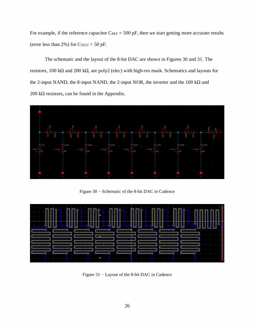
The schematic and the layout of the 8-bit DAC are shown in Figures 30 and 31. The
resistors, 100 kΩ and 200 kΩ, are poly2 (elec) with high-res mask. Schematics and layouts for
the 2-input NAND, the 8-input NAND, the 2-input NOR, the inverter and the 100 kΩ and
200 kΩ resistors, can be found in the Appendix.
Figure 30 − Schematic of the 8-bit DAC in Cadence
Figure 31 − Layout of the 8-bit DAC in Cadence

27
CHAPTER 3: THE CHIP
In Chapter 2, we reviewed every part of the circuit separately. The entire chip along with
the bonding pads is shown in Figure 32. The bonding pads have Electrostatic Discharge (ESD)
protection and there is a 1 pF decoupling capacitor between VDD and GND.
Figure 32 − Schematic of the chip with the bonding pads
28
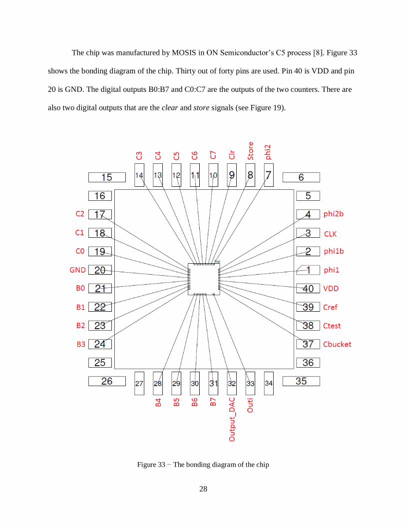
The chip was manufactured by MOSIS in ON Semiconductor’s C5 process [8]. Figure 33
shows the bonding diagram of the chip. Thirty out of forty pins are used. Pin 40 is VDD and pin
20 is GND. The digital outputs B0:B7 and C0:C7 are the outputs of the two counters. There are
also two digital outputs that are the clear and store signals (see Figure 19).
Figure 33 − The bonding diagram of the chip
29
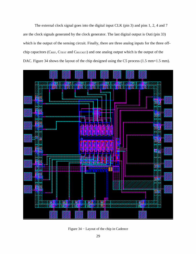
The external clock signal goes into the digital input CLK (pin 3) and pins 1, 2, 4 and 7
are the clock signals generated by the clock generator. The last digital output is Outi (pin 33)
which is the output of the sensing circuit. Finally, there are three analog inputs for the three off-
chip capacitors (CREF, CTEST and CBUCKET) and one analog output which is the output of the
DAC. Figure 34 shows the layout of the chip designed using the C5 process (1.5 mm×1.5 mm).
Figure 34 − Layout of the chip in Cadence
30
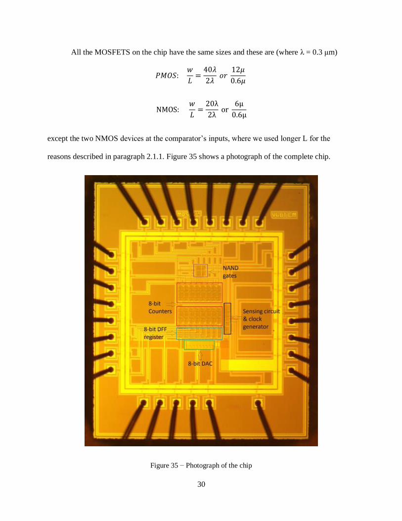
All the MOSFETS on the chip have the same sizes and these are (where λ = 0.3 μm)
𝑃𝑀𝑂𝑆: 𝑤
𝐿=
40𝜆
2𝜆 𝑜𝑟
12𝜇
0.6𝜇
NMOS: 𝑤
𝐿=
20λ
2λ or
6μ
0.6μ
except the two NMOS devices at the comparator’s inputs, where we used longer L for the
reasons described in paragraph 2.1.1. Figure 35 shows a photograph of the complete chip.
Figure 35 − Photograph of the chip
31
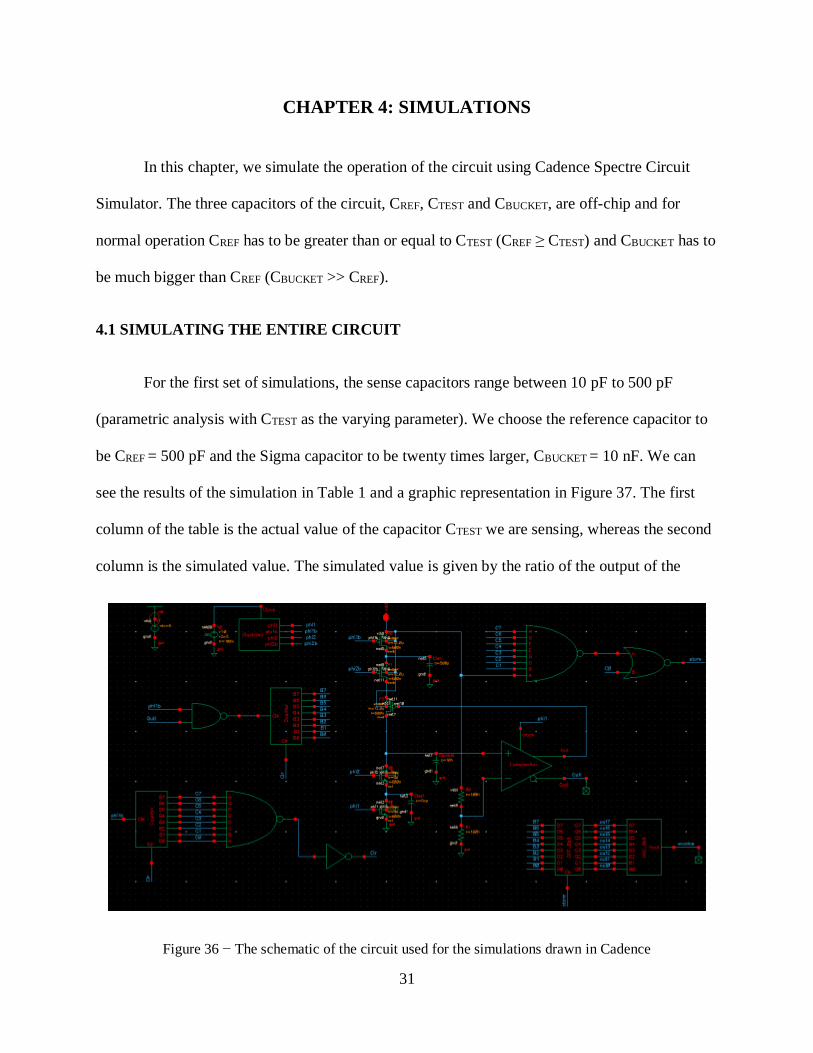
CHAPTER 4: SIMULATIONS
In this chapter, we simulate the operation of the circuit using Cadence Spectre Circuit
Simulator. The three capacitors of the circuit, CREF, CTEST and CBUCKET, are off-chip and for
normal operation CREF has to be greater than or equal to CTEST (CREF ≥ CTEST) and CBUCKET has to
be much bigger than CREF (CBUCKET >> CREF).
4.1 SIMULATING THE ENTIRE CIRCUIT
For the first set of simulations, the sense capacitors range between 10 pF to 500 pF
(parametric analysis with CTEST as the varying parameter). We choose the reference capacitor to
be CREF = 500 pF and the Sigma capacitor to be twenty times larger, CBUCKET = 10 nF. We can
see the results of the simulation in Table 1 and a graphic representation in Figure 37. The first
column of the table is the actual value of the capacitor CTEST we are sensing, whereas the second
column is the simulated value. The simulated value is given by the ratio of the output of the
Figure 36 − The schematic of the circuit used for the simulations drawn in Cadence

32
DAC to the power supply voltage (VDD) times the value of the reference capacitance CREF.
Finally, the third column is the error in percentage of the sensing circuit and the fourth is the
power dissipation of the circuit. Figure 36 shows the schematic used to run the simulations.
Actual Value (in pF) Simulated Value (in pF) Error (%) Power (in μW)
10 11.8 18% 338
50 50.9 1.8% 355
100 101.7 1.7% 381
150 152.5 1.67% 406
200 203.2 1.6% 425
250 249.7 0.12% 451
300 300.7 0.23% 475
350 343.6 1.83% 498
400 398.3 0.42% 522
450 449.1 0.2% 545
500 496.1 0.78% 560
Table 1 – Parametric analysis results for CTEST varying from 10 pF to 500 pF
Figure 37 − Simulation results for CTEST varying from 10 pF to 500 pF
0.00%
2.00%
4.00%
6.00%
8.00%
10.00%
12.00%
14.00%
16.00%
18.00%
20.00%
0
50
100
150
200
250
300
350
400
450
500
0 50 100 150 200 250 300 350 400 450 500
Actual Value (pF) Simulated Value (pF) Error

33
For the second set of simulations, we are trying to sense capacitors that range between
500 pF to 1 nF. We choose the reference capacitor to be CREF = 1 nF and the Sigma capacitor to
be CBUCKET = 20 nF. We can see the results of the simulation in Table 2 and Figure 38.
Actual value (in pF) Simulated Value (in pF) Error (%) Power (in μW)
500 499.5 0.11% 524
550 550.4 0.08% 556
600 605.2 0.87% 578
650 640.3 1.49% 602
700 699 0.14% 621
750 749.5 0.07% 648
800 796.5 0.44% 675
850 843.5 0.77% 698
900 898.2 0.2% 719
950 949.3 0.07% 735
1000 992.2 0.78% 752
Table 2 – Parametric analysis results for CTEST varying from 500 pF to 1 nF
Figure 38 − Simulation results for CTEST varying from 500 pF to 1 nF
0.00%
2.00%
4.00%
6.00%
8.00%
10.00%
12.00%
14.00%
16.00%
18.00%
20.00%
500
550
600
650
700
750
800
850
900
950
1000
500 550 600 650 700 750 800 850 900 950 1000
Actual Value (pF) Simulated Value (pF) Error

34
4.2 SIMULATING THE SENSING CIRCUIT (WITHOUT PERIPHERAL CIRCUITRY)
Next, we simulate the operation of the sensing circuit exclusively without the peripheral
circuitry (counters, DFFs, logic gates and DAC). We run the simulation for 256 clock cycles and
then take the average of the comparator’s complement output Outi. Finally, we multiply that
voltage with 𝐶𝑅𝐸𝐹 𝑉𝐷𝐷⁄ and get the simulated value for CTEST. Figure 39 shows the schematic
we used to simulate the operation of the sensing circuit.
Figure 39 − The schematic used to simulate the sensing circuit without the peripheral circuitry
Figures 40 and 41 show the results of the simulations for different values of CTEST
ranging from 50 pF to 1 nF. It is clear that the output of the circuit changes linearly with different
capacitors CTEST.
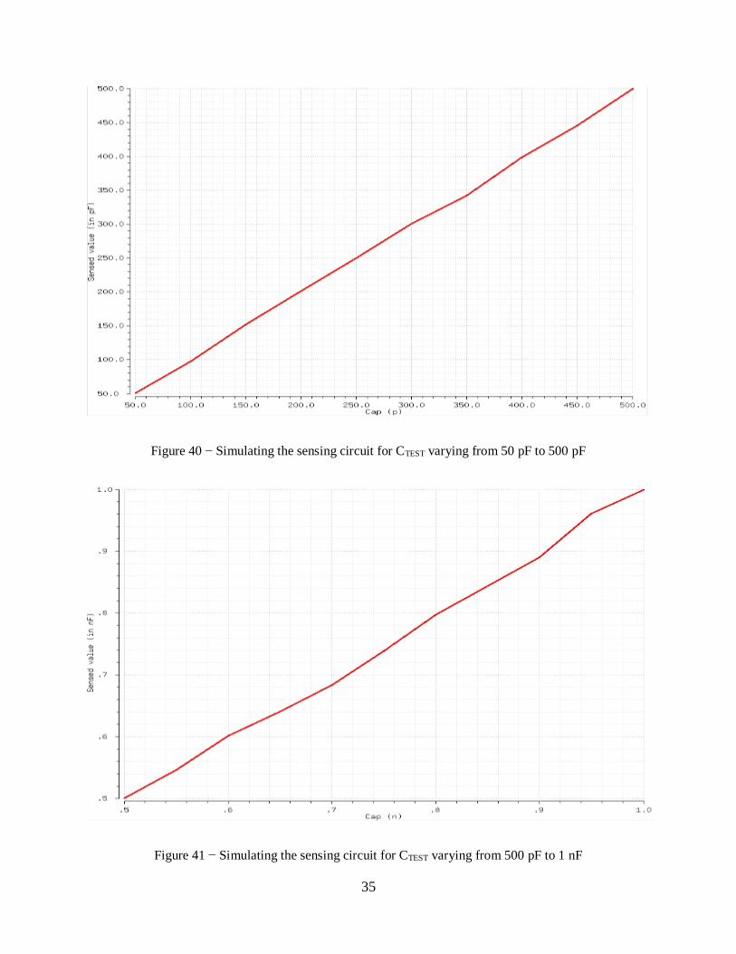
35
Figure 40 − Simulating the sensing circuit for CTEST varying from 50 pF to 500 pF
Figure 41 − Simulating the sensing circuit for CTEST varying from 500 pF to 1 nF

36
4.3 SENSING LARGER CAPACITORS
Up to this point, we only simulated the circuit with CTEST in the range of interest for our
applications (10 pF-1 nF). Now, let us try to simulate the circuit with bigger capacitors, from
50 nF to 1 μF. Although this chip will not be tested for big capacitors, simulating its operation
might be interesting and helpful.
For the first set of simulations, CTEST is varying between 10 nF and 500 nF, CREF is
500 nF and CBUCKET is now 10 μF. With these large capacitors, in order for the switched-
capacitors to work properly, we must adjust the clock frequency to a lower level. From Eq. (2.3),
the switched-capacitor resistor is
𝑅𝑆𝐶 =1
𝐶×𝑓
Now that the capacitor value increases, we have to lower the clock frequency so that RSC remains
large. The clock frequency was at 33 kHz for all the previous simulations and now we drop it to
33 Hz. Table 3 and Figure 42 show the results of these simulations.
Actual Value (in nF) Simulated Value (in nF) Error (%) Power (in μW)
10 11.8 18% 284
50 50.9 1.84% 301
100 101.7 1.7% 326
150 156.3 4.2% 353
200 201.3 0.65% 378
250 249.7 0.12% 401
300 302.6 0.87% 425
350 343.6 1.83% 449
400 398.3 0.42% 474
450 451 0.22% 502
500 496.1 0.78% 521
Table 3 − Parametric analysis results for CTEST varying from 10 nF to 500 nF

37
Figure 42 − Simulation results for CTEST varying from 10 nF to 500 nF
By simulating the sensing circuit without the peripherals, we get a similar graph (see Figure 43).
Figure 43 − Simulating the sensing circuit for CTEST varying from 50 nF to 500 nF
0.00%
2.00%
4.00%
6.00%
8.00%
10.00%
12.00%
14.00%
16.00%
18.00%
20.00%
0
50
100
150
200
250
300
350
400
450
500
0 50 100 150 200 250 300 350 400 450 500
Actual Value (nF) Simulated Value (nF) Error
38
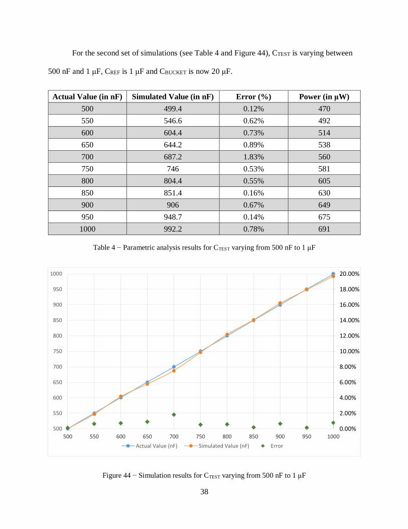
For the second set of simulations (see Table 4 and Figure 44), CTEST is varying between
500 nF and 1 μF, CREF is 1 μF and CBUCKET is now 20 μF.
Actual Value (in nF) Simulated Value (in nF) Error (%) Power (in μW)
500 499.4 0.12% 470
550 546.6 0.62% 492
600 604.4 0.73% 514
650 644.2 0.89% 538
700 687.2 1.83% 560
750 746 0.53% 581
800 804.4 0.55% 605
850 851.4 0.16% 630
900 906 0.67% 649
950 948.7 0.14% 675
1000 992.2 0.78% 691
Table 4 − Parametric analysis results for CTEST varying from 500 nF to 1 μF
Figure 44 − Simulation results for CTEST varying from 500 nF to 1 μF
0.00%
2.00%
4.00%
6.00%
8.00%
10.00%
12.00%
14.00%
16.00%
18.00%
20.00%
500
550
600
650
700
750
800
850
900
950
1000
500 550 600 650 700 750 800 850 900 950 1000
Actual Value (nF) Simulated Value (nF) Error

39
Figure 44 shows the simulation results for CTEST varying from 500 nF to 1 μF, whereas
Figure 45 shows the results of simulating just the sensing circuit for the same range of CTEST
without the peripheral circuitry.
Figure 45 − Simulating the sensing circuit for CTEST varying from 500 nF to 1 μF
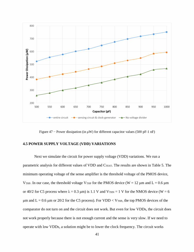
4.4 POWER DISSIPATION
A very important information about the circuit is the average power dissipation, in other
words the power supply voltage VDD (which is 5 V for the C5 process) multiplied by the power
supply current IDD over time. Figures 46 and 47 show graphs of the power dissipation for
different capacitor values. The blue line indicates the power for the entire circuit, whereas the
orange line shows the power for the sensing circuit and the non-overlapping clock generator
without the peripheral circuitry. Clearly, the larger the CTEST, the more power the circuit needs.

40
In order to get the reference voltage VREF, which is VDD/2 = 2.5 V, used in the negative
input of the comparator, we use a voltage divider with two 100k resistors. This circuitry
dissipates a lot of power (𝐼 = 𝑉𝐷𝐷 200𝑘𝛺⁄ = 25𝜇𝛢, 𝑠𝑜 𝑃 = 𝑉𝐷𝐷×𝐼 = 125𝜇𝑊) and we could
have avoided it by using an external input signal of 2.5 V. The green line represents the power of
the sensing circuit and the clock generator (no peripheral circuitry) minus the power dissipated
by the voltage divider (125 μW).
Figure 46 − Power dissipation (in μW) for different capacitor values (10 pF-500 pF)
The average power dissipation ranges between 300-700 μW approximately for frequency
f = 33 kHz and CTEST in the pico-Farad region. When we change frequency to 33Hz in order to
sense bigger capacitors in the nano-Farad region, the average power dissipation remains in the
same range, 300-700 μW (see Tables 3 and 4).
0
100
200
300
400
500
600
0 50 100 150 200 250 300 350 400 450 500
Po
wer
Dis
sip
atio
n (μ
W)
Capacitor (pF)
entire circuit sensing circuit & clock-generator No voltage divider
41
Figure 47 − Power dissipation (in μW) for different capacitor values (500 pF-1 nF)
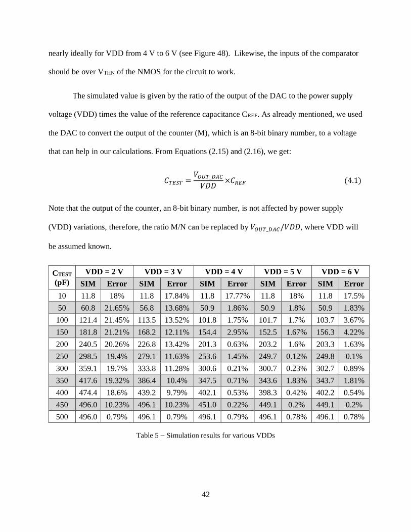
4.5 POWER SUPPLY VOLTAGE (VDD) VARIATIONS
Next we simulate the circuit for power supply voltage (VDD) variations. We run a
parametric analysis for different values of VDD and CTEST. The results are shown in Table 5. The
minimum operating voltage of the sense amplifier is the threshold voltage of the PMOS device,
VTHP. In our case, the threshold voltage VTHP for the PMOS device (W = 12 μm and L = 0.6 μm
or 40/2 for C5 process where λ = 0.3 μm) is 1.1 V and VTHN = 1 V for the NMOS device (W = 6
μm and L = 0.6 μm or 20/2 for the C5 process). For VDD < VTHP, the top PMOS devices of the
comparator do not turn on and the circuit does not work. But even for low VDDs, the circuit does
not work properly because there is not enough current and the sense is very slow. If we need to
operate with low VDDs, a solution might be to lower the clock frequency. The circuit works
200
300
400
500
600
700
800
500 550 600 650 700 750 800 850 900 950 1000
Po
wer
Dis
sip
atio
n (μ
W)
Capacitor (pF)
entire circuit sensing circuit & clock-generator No voltage divider
42
nearly ideally for VDD from 4 V to 6 V (see Figure 48). Likewise, the inputs of the comparator
should be over VTHN of the NMOS for the circuit to work.
The simulated value is given by the ratio of the output of the DAC to the power supply
voltage (VDD) times the value of the reference capacitance CREF. As already mentioned, we used
the DAC to convert the output of the counter (M), which is an 8-bit binary number, to a voltage
that can help in our calculations. From Equations (2.15) and (2.16), we get:
𝐶𝑇𝐸𝑆𝑇 =𝑉𝑂𝑈𝑇_𝐷𝐴𝐶
𝑉𝐷𝐷×𝐶𝑅𝐸𝐹 (4.1)
Note that the output of the counter, an 8-bit binary number, is not affected by power supply
(VDD) variations, therefore, the ratio M/N can be replaced by 𝑉𝑂𝑈𝑇_𝐷𝐴𝐶/𝑉𝐷𝐷, where VDD will
be assumed known.
CTEST
(pF)
VDD = 2 V VDD = 3 V VDD = 4 V VDD = 5 V VDD = 6 V
SIM Error SIM Error SIM Error SIM Error SIM Error
10 11.8 18% 11.8 17.84% 11.8 17.77% 11.8 18% 11.8 17.5%
50 60.8 21.65% 56.8 13.68% 50.9 1.86% 50.9 1.8% 50.9 1.83%
100 121.4 21.45% 113.5 13.52% 101.8 1.75% 101.7 1.7% 103.7 3.67%
150 181.8 21.21% 168.2 12.11% 154.4 2.95% 152.5 1.67% 156.3 4.22%
200 240.5 20.26% 226.8 13.42% 201.3 0.63% 203.2 1.6% 203.3 1.63%
250 298.5 19.4% 279.1 11.63% 253.6 1.45% 249.7 0.12% 249.8 0.1%
300 359.1 19.7% 333.8 11.28% 300.6 0.21% 300.7 0.23% 302.7 0.89%
350 417.6 19.32% 386.4 10.4% 347.5 0.71% 343.6 1.83% 343.7 1.81%
400 474.4 18.6% 439.2 9.79% 402.1 0.53% 398.3 0.42% 402.2 0.54%
450 496.0 10.23% 496.1 10.23% 451.0 0.22% 449.1 0.2% 449.1 0.2%
500 496.0 0.79% 496.1 0.79% 496.1 0.79% 496.1 0.78% 496.1 0.78%
Table 5 − Simulation results for various VDDs
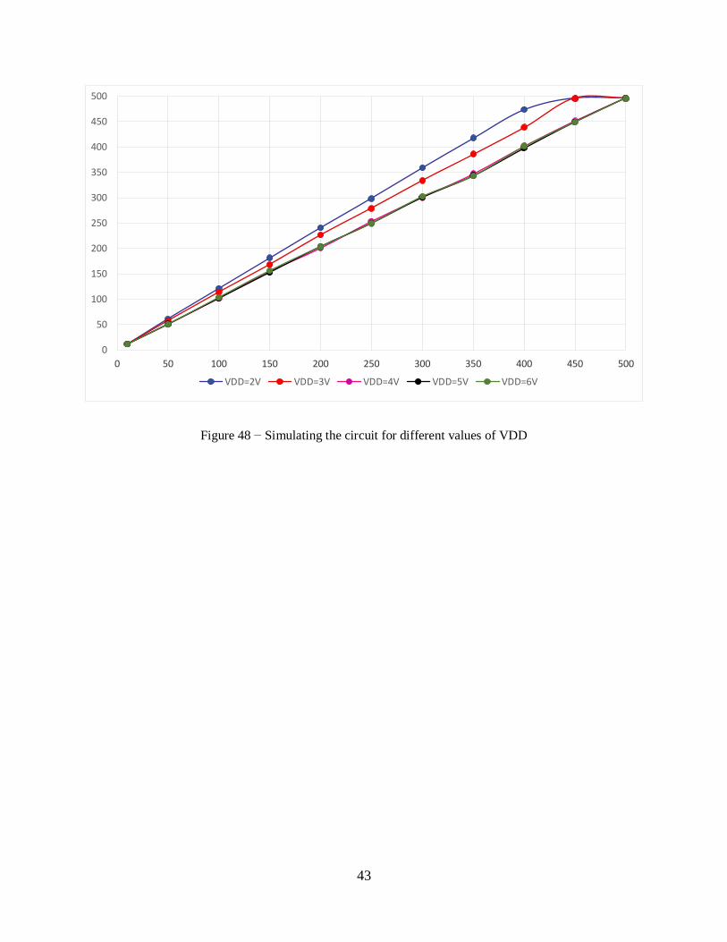
43
Figure 48 − Simulating the circuit for different values of VDD
0
50
100
150
200
250
300
350
400
450
500
0 50 100 150 200 250 300 350 400 450 500
VDD=2V VDD=3V VDD=4V VDD=5V VDD=6V
44
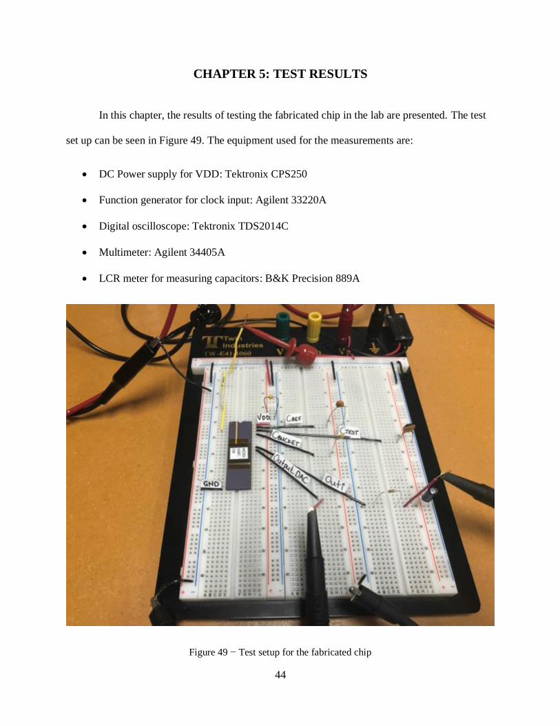
CHAPTER 5: TEST RESULTS
In this chapter, the results of testing the fabricated chip in the lab are presented. The test
set up can be seen in Figure 49. The equipment used for the measurements are:
• DC Power supply for VDD: Tektronix CPS250
• Function generator for clock input: Agilent 33220A
• Digital oscilloscope: Tektronix TDS2014C
• Multimeter: Agilent 34405A
• LCR meter for measuring capacitors: B&K Precision 889A
Figure 49 − Test setup for the fabricated chip

45
5.1 CAPACITORS IN THE pF RANGE
We start the testing by using a 522 pF capacitor as reference capacitor CREF, a 10.3 nF
capacitor as “bucket” capacitor CBUCKET and an input clock signal of 30 kHz. We use an
oscilloscope probe to observe the output of the DAC (Output_DAC) and another probe to
observe the inverted output of the sensing circuit (Outi) through an RC averaging filter (R = 1
MΩ and C = 1 μF). Finally, a 100 nF decoupling capacitor is used between VDD and ground to
avoid noise interference.
For the circuit’s proper operation, we must ensure that CREF settles completely between
the clock changes and that the voltage VBUCKET at CBUCKET moves around the reference voltage
VREF which is VDD/2 (VREF = 2.5 V for VDD = 5V). From the first measurements, it is clear that
VBUCKET is not at 2.5 V but at 3 V, probably due to a faulty voltage divider. Due to this variation,
the equations that describe the operation of the sensing circuit must be adjusted.
Equation (2.10), using Equations (2.6) and (2.7), becomes:
𝑉𝐵𝑈𝐶𝐾𝐸𝑇
𝑅𝑇𝐸𝑆𝑇=
𝑉𝐷𝐷 − 𝑉𝐵𝑈𝐶𝐾𝐸𝑇
𝑅𝑅𝐸𝐹×
𝑀
𝑁 (5.1)
𝑅𝑅𝐸𝐹
𝑅𝑇𝐸𝑆𝑇=
𝑉𝐷𝐷 − 𝑉𝐵𝑈𝐶𝐾𝐸𝑇
𝑉𝐵𝑈𝐶𝐾𝐸𝑇×
𝑀
𝑁 (5.2)
1𝐶𝑅𝐸𝐹×𝑓
1𝐶𝑇𝐸𝑆𝑇×𝑓
=𝑉𝐷𝐷 − 𝑉𝐵𝑈𝐶𝐾𝐸𝑇
𝑉𝐵𝑈𝐶𝐾𝐸𝑇×
𝑀
𝑁 (5.3)
𝐶𝑇𝐸𝑆𝑇 = 𝐶𝑅𝐸𝐹×𝑀
𝑁×
𝑉𝐷𝐷 − 𝑉𝐵𝑈𝐶𝐾𝐸𝑇
𝑉𝐵𝑈𝐶𝐾𝐸𝑇 (5.4)
46
Comparing Equation (5.4) to (2.15), we notice the extra term (VDD-VBUCKET)/VBUCKET. In this
case, VBUCKET = 3 V and VDD = 5 V, so our measurements should be multiplied by 2/3 to reflect
the correct value. The formulas used to translate the output voltages into capacitor values are
𝑆𝑒𝑛𝑠𝑖𝑛𝑔 𝑐𝑖𝑟𝑐𝑢𝑖𝑡: 𝐶𝑇𝐸𝑆𝑇 =2
3×𝑉𝑂𝑢𝑡𝑖×
𝐶𝑅𝐸𝐹
5 (5.5)
𝐷𝐴𝐶: 𝐶𝑇𝐸𝑆𝑇 =2
3×𝑉𝑂𝑢𝑡𝑝𝑢𝑡_𝐷𝐴𝐶×
𝐶𝑅𝐸𝐹
𝑉𝐷𝐷 (5.6)
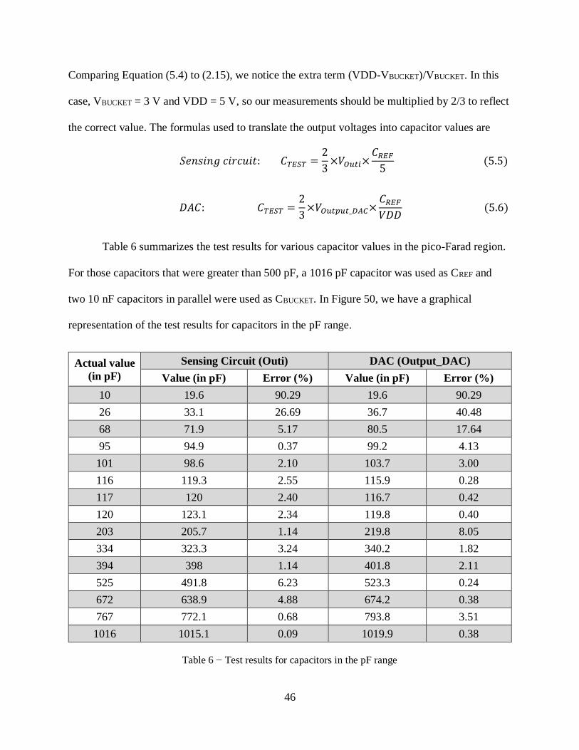
Table 6 summarizes the test results for various capacitor values in the pico-Farad region.
For those capacitors that were greater than 500 pF, a 1016 pF capacitor was used as CREF and
two 10 nF capacitors in parallel were used as CBUCKET. In Figure 50, we have a graphical
representation of the test results for capacitors in the pF range.
Actual value
(in pF)
Sensing Circuit (Outi) DAC (Output_DAC)
Value (in pF) Error (%) Value (in pF) Error (%)
10 19.6 90.29 19.6 90.29
26 33.1 26.69 36.7 40.48
68 71.9 5.17 80.5 17.64
95 94.9 0.37 99.2 4.13
101 98.6 2.10 103.7 3.00
116 119.3 2.55 115.9 0.28
117 120 2.40 116.7 0.42
120 123.1 2.34 119.8 0.40
203 205.7 1.14 219.8 8.05
334 323.3 3.24 340.2 1.82
394 398 1.14 401.8 2.11
525 491.8 6.23 523.3 0.24
672 638.9 4.88 674.2 0.38
767 772.1 0.68 793.8 3.51
1016 1015.1 0.09 1019.9 0.38
Table 6 − Test results for capacitors in the pF range

47
Figure 50 − Graphical representation of test results for capacitors in the pF range
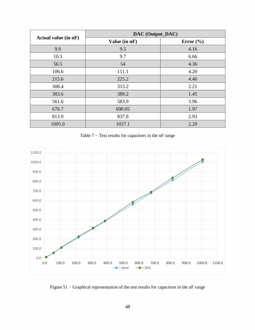
5.2 CAPACITORS IN THE nF RANGE
Next we tested larger value capacitors using a 561.6 nF capacitor as reference capacitor
CREF, a 9.4 μF capacitor as “bucket” capacitor CBUCKET and an input clock signal of 30 Hz. Due
to the low frequency, an RC filter averaging the inverted output of the sensing circuit (Outi) was
impractically slow, so we only measured the output of the DAC (Output_DAC). For those
capacitors that were greater than 500 nF, a 1005 nF capacitor was used as CREF and two 10 μF
capacitors in parallel were used as CBUCKET. Table 7 summarizes the test results for various
capacitor values in the nano-Farad region and Figure 51 shows a graphical representation of
those test results.
0
100
200
300
400
500
600
700
800
900
1000
1100
0 100 200 300 400 500 600 700 800 900 1000 1100
Ideal Sensing Circuit DAC
48
Actual value (in nF) DAC (Output_DAC)
Value (in nF) Error (%)
9.9 9.5 4.16
10.3 9.7 6.66
56.5 54 4.36
106.6 111.1 4.20
215.6 225.2 4.46
308.4 315.2 2.21
383.6 389.2 1.45
561.6 583.9 3.96
676.7 690.05 1.97
813.9 837.8 2.93
1005.0 1027.1 2.20
Table 7 − Test results for capacitors in the nF range
Figure 51 − Graphical representation of the test results for capacitors in the nF range
0.0
100.0
200.0
300.0
400.0
500.0
600.0
700.0
800.0
900.0
1000.0
1100.0
0.0 100.0 200.0 300.0 400.0 500.0 600.0 700.0 800.0 900.0 1000.0 1100.0
ideal DAC

49
5.3 POWER DISSIPATION
Next, we tested the power dissipation of the fabricated chip by measuring the current
draw by the circuit and multiplying it with VDD = 5 V. Note that the circuit needs more power to
sense larger capacitors. Also note that the circuit needs the same power to sense pF capacitors
and nF capacitors, since the clock frequency drops 1000 times when the capacitor value
increases 1000 times (see Table 8 and Figure 52).
pF nF
CTEST (in pF) Power (in μW) CTEST (in nF) Power (in μW)
10 343 9.9 311
101 387 106.6 377
203 423 308.4 449
394 503 383.6 483
672 607 561.6 512
1016 667 1005.0 641
Table 8 − Test results for power dissipation
Figure 52 − Test results for power dissipation
0
100
200
300
400
500
600
700
0 100 200 300 400 500 600 700 800 900 1000 1100
Po
wer
Dis
sip
atio
n (
in μ
W)
Capacitor value
pF range nF range
50
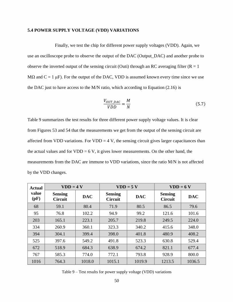
5.4 POWER SUPPLY VOLTAGE (VDD) VARIATIONS
Finally, we test the chip for different power supply voltages (VDD). Again, we
use an oscilloscope probe to observe the output of the DAC (Output_DAC) and another probe to
observe the inverted output of the sensing circuit (Outi) through an RC averaging filter (R = 1
MΩ and C = 1 μF). For the output of the DAC, VDD is assumed known every time since we use
the DAC just to have access to the M/N ratio, which according to Equation (2.16) is
𝑉𝑂𝑈𝑇_𝐷𝐴𝐶
𝑉𝐷𝐷=
𝑀
𝑁 (5.7)
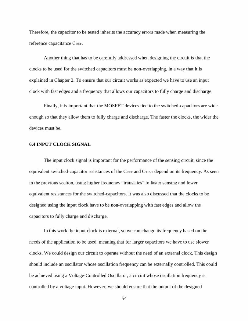
Table 9 summarizes the test results for three different power supply voltage values. It is clear
from Figures 53 and 54 that the measurements we get from the output of the sensing circuit are
affected from VDD variations. For VDD = 4 V, the sensing circuit gives larger capacitances than
the actual values and for VDD = 6 V, it gives lower measurements. On the other hand, the
measurements from the DAC are immune to VDD variations, since the ratio M/N is not affected
by the VDD changes.
Actual
value
(pF)
VDD = 4 V VDD = 5 V VDD = 6 V
Sensing
Circuit DAC
Sensing
Circuit DAC
Sensing
Circuit DAC
68 59.1 80.4 71.9 80.5 86.5 79.6
95 76.8 102.2 94.9 99.2 121.6 101.6
203 165.1 223.1 205.7 219.8 249.5 224.0
334 260.9 360.1 323.3 340.2 415.6 348.0
394 304.1 399.4 398.0 401.8 480.9 408.2
525 397.6 549.2 491.8 523.3 630.8 529.4
672 518.9 684.3 638.9 674.2 821.1 677.4
767 585.3 774.0 772.1 793.8 928.9 800.0
1016 764.3 1018.0 1015.1 1019.9 1213.5 1036.5
Table 9 – Test results for power supply voltage (VDD) variations
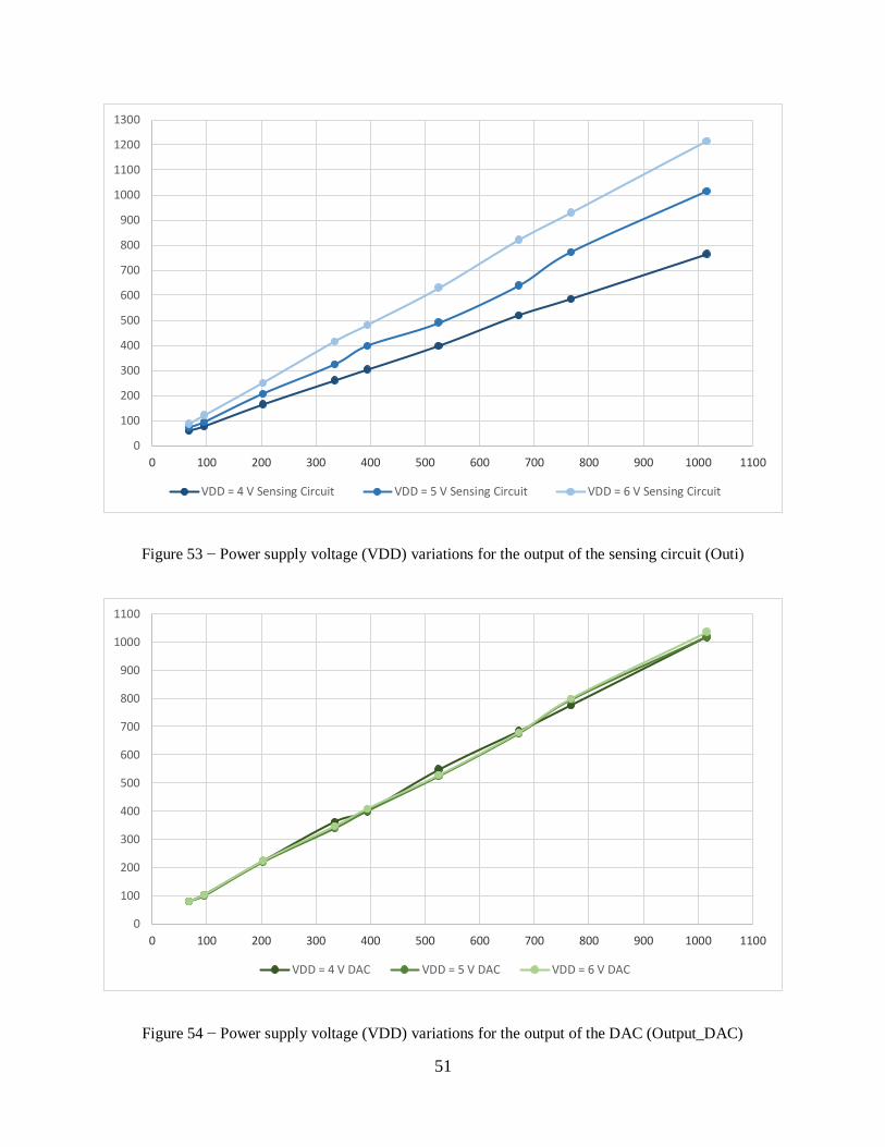
51
Figure 53 − Power supply voltage (VDD) variations for the output of the sensing circuit (Outi)
Figure 54 − Power supply voltage (VDD) variations for the output of the DAC (Output_DAC)
0
100
200
300
400
500
600
700
800
900
1000
1100
1200
1300
0 100 200 300 400 500 600 700 800 900 1000 1100
VDD = 4 V Sensing Circuit VDD = 5 V Sensing Circuit VDD = 6 V Sensing Circuit
0
100
200
300
400
500
600
700
800
900
1000
1100
0 100 200 300 400 500 600 700 800 900 1000 1100
VDD = 4 V DAC VDD = 5 V DAC VDD = 6 V DAC

52
CHAPTER 6: DESIGN DISCUSSION
6.1 VOLTAGE AT THE “BUCKET” CAPACITOR (VBUCKET)
In Chapter 5, we saw that the voltage at the bucket capacitor CBUCKET is more than what it
should be for proper operation. This is due to two reasons:
• We used a 130mV offset at the comparator, which may have not created a problem in the
simulations (it has actually made the simulation results a little better than when using a
comparator without an offset), but in reality, it can only create problems, because it
moves the voltage at the bucket capacitor CBUCKET away from the desired VDD/2 value.
Moreover, the designed offset value may be different than its actual value due to process
variations.
• The unsilicided polysilicon resistors used for the voltage divider, that gives the reference
voltage (VREF) used as input to the comparator, were designed to be equal (100k), so that
they can give an output of VDD/2. However, they typically provide an actual resistance
value that can vary +/- 30% or more from the value that they are designed to be [10].
The first design problem can be solved by using a comparator without an offset. The
second one, is more complicated to be addressed, because it is a process failure. One way to
address this problem would be to use wider resistors. This would minimize the linewidth
uncertainties that are result of lithographic and etching variation. In addition to that, the
resistance variation could be compensated by providing additional polysilicon resistors which
can be switched in or out, in series or parallel with the target resistor. For the purposes of testing
the operation of the sensing circuit, an output pin giving access to the non-inverting input of the
comparator would allow us to accurately measure its potential and adjust it to the desired value.

53
6.2 COMPARATOR
The comparator has to be designed without an offset, so that the voltage at the bucket
capacitor CBUCKET will be around VDD/2 as desired for proper sensing operation. Moreover, the
impedance at the input nodes of the comparator should be the same. Non-matching input
impedances could lead to wrong decisions, since one input will be moving faster than the other.
A capacitor with value equal to CBUCKET should be used at the non-inverting input of the
comparator. This would ensure input impedance matching for the comparator and would reduce
variations of the reference voltage VREF.
6.3 SWITCHED CAPACITORS
Τhe value of a switched capacitor can be “translated” according to Equation (2.3) to an
equivalent resistance of
𝑅𝑆𝐶 =1
𝑓×𝐶
We have already shown that the capacitance to be measured is related to CREF by Equation (2.15)
𝐶𝑇𝐸𝑆𝑇 = 𝐶𝑅𝐸𝐹×𝑀
𝑁
It is clear that the way our circuit works depends on the accuracy of the CREF value. If we name
the percentage error in capacitance of the reference capacitor CREF,ERROR and CTEST,ERROR is the
resulting percentage error in the capacitance to be measured then
𝐶𝑇𝐸𝑆𝑇×(1 + 𝐶𝑇𝐸𝑆𝑇,𝐸𝑅𝑅𝑂𝑅) =𝑀
𝑁×𝐶𝑅𝐸𝐹×(1 + 𝐶𝑅𝐸𝐹,𝐸𝑅𝑅𝑂𝑅)
=> 𝐶𝑇𝐸𝑆𝑇,𝐸𝑅𝑅𝑂𝑅 = 𝐶𝑅𝐸𝐹,𝐸𝑅𝑅𝑂𝑅 (6.1)
54
Therefore, the capacitor to be tested inherits the accuracy errors made when measuring the
reference capacitance CREF.
Another thing that has to be carefully addressed when designing the circuit is that the
clocks to be used for the switched capacitors must be non-overlapping, in a way that it is
explained in Chapter 2. To ensure that our circuit works as expected we have to use an input
clock with fast edges and a frequency that allows our capacitors to fully charge and discharge.
Finally, it is important that the MOSFET devices tied to the switched-capacitors are wide
enough so that they allow them to fully charge and discharge. The faster the clocks, the wider the
devices must be.
6.4 INPUT CLOCK SIGNAL
The input clock signal is important for the performance of the sensing circuit, since the
equivalent switched-capacitor resistances of the CREF and CTEST depend on its frequency. As seen
in the previous section, using higher frequency “translates” to faster sensing and lower
equivalent resistances for the switched-capacitors. It was also discussed that the clocks to be
designed using the input clock have to be non-overlapping with fast edges and allow the
capacitors to fully charge and discharge.
In this work the input clock is external, so we can change its frequency based on the
needs of the application to be used, meaning that for larger capacitors we have to use slower
clocks. We could design our circuit to operate without the need of an external clock. This design
should include an oscillator whose oscillation frequency can be externally controlled. This could
be achieved using a Voltage-Controlled Oscillator, a circuit whose oscillation frequency is
controlled by a voltage input. However, we should ensure that the output of the designed
55
oscillator will have a frequency that can range between 30 Hz, which is the frequency we used to
test the nano-range capacitors, and 30 kHz, which is the frequency we used to test pico-range
capacitors.
Another approach to designing the clock oscillator would be to design two distinct
oscillators, one working at the Hz range and one working in the kHz range. The user, could
choose the one to be used based on the application.
6.5 COUNTER
In this design, an 8-bit asynchronous counter with D-FFs has been used. The counter
allows the circuit to estimate the tested capacitance effectively with power supply voltage
variations, as we saw in the testing section, at the cost of more circuitry and the consequent
increased power dissipation. As we derived in Chapter 2, Equation (2.22), if we want to keep the
estimated capacitance error created by the counter within 2%, the CTEST cannot be less than 10%
of the CREF. If we want to increase the range of the capacitances that can be tested using the same
reference, we have to use a counter with more bits.
6.6 POWER DISSIPATION
We have seen in the power dissipation sections that the power dissipation of our circuit
depends on the value of the capacitor to be tested (CTEST). This is because CTEST can be
“translated” to an equivalent resistance that depends on the clock frequency and its capacitance.
Knowing that the sensing circuit will match the equivalent resistance of CTEST (RTEST) with the
equivalent resistance of CREF (RREF), as can be seen in Figure 11 and the associated discussion,
56
the total resistance between VDD and ground in the sensing circuit (excluding the comparator)
will be 2×𝑅𝑇𝐸𝑆𝑇. Hence, the power dissipation in the “heart” of our sensing circuit will be
𝑃 =𝑉𝐷𝐷2
2×𝑅𝑇𝐸𝑆𝑇=
𝑉𝐷𝐷2
2×𝑓×𝐶𝑇𝐸𝑆𝑇 (6.2)
If we keep f constant, it is clear that the power dissipation increases linearly with
increasing CTEST. This is what we have already seen in Figures 46 and 47. If we want to decrease
the power dissipation in this part of the circuit, we could either decrease the power supply
voltage VDD or the clock frequency f. Both solutions have limitations.
If we decrease the power supply voltage, the CMOS devices will “open” less (smaller
source-to-gate voltages) and this will result, after a point, in not fully charging and discharging
capacitors. The problem with the reduced frequency is reduced sensing speed. Therefore, as
always, we have to balance speed and power dissipation based on the specific needs of the
application.
Except for the power dissipation in the switched-capacitors, there is also power
dissipation in the voltage divider. In this work, it was designed to be using 100k resistor, so its
power dissipation is 125μW. This can be reduced if we use bigger resistances, at the cost of more
layout area.
Clock-generator, comparator and peripheral circuitry also draw some current. This can be
reduced by increasing the length of the devices. We know that the current in CMOS decreases
for less wide or longer devices [4].
𝐼𝐷 ∝𝑊
𝐿 (6.3)
57
If we want to reduce the power dissipation, we can either decrease the width (W) or
increase the length (L). Since we can’t decrease the width more than the minimum allowed from
the process, the safest way to reduce the current in devices is by increasing the length.
Finally, we could reduce power dissipation even further if we did not include the counter,
the D-FFs and the DAC in our design. However, if we omit this part of the circuit, we must
ensure that the power supply voltage is constant and at a known value during operation. Also, we
must use an RC filter to average the output of the comparator. The large time constant of this
filter can make our circuit impractically slow for large capacitors, where we need slower clocks.

58
CHAPTER 7: APPLICATIONS
For the applications of the capacitive sensing circuit presented in the previous chapters,
we used a capacitive sensor made on printed circuit board (PCB). It contains a number of co-
planar plate capacitors in parallel. Capacitance sums in parallel, so this will lead to a larger
capacity of the entire assembly and therefore a larger capacity swing when the dielectric
changes. The reason we used a co-planar plate capacitor, instead of the standard parallel plate
capacitor is that we do not have to get the soil/moisture to occupy the gap in the middle. The
electric field lines extend outward from the plates into the dielectric on both sides. The PCB was
designed using Eagle software and it was ordered through DorkbotPDX PCB Order [11].
Figure 55 − Two different types of capacitor configurations
Figure 56 − The capacitive sensor

59
Figure 57 − The sensor as designed in Eagle [11]
7.1 CAPACITIVE WATER LEVEL SENSOR
The first application of the sensing circuit is to measure water level in a container in
relation to capacitance. For this application, we use the capacitive sensor presented above in the
test setup shown in Figure 58. In this case, water is the dielectric. We expect that the higher the
water level, the larger the capacitance since water has a bigger dielectric constant than air.
Figure 58 − Test setup for capacitive water level sensing
60
The capacitive sensor is mounted on the container wall. We gradually add water in the
container and measure the capacitance of the sensor using a handheld multimeter (EXTECH
MiniTec 26). Then we put the leads of the sensor on the breadboard and take the circuit’s
measurements.
Water level
(in cm)
Multimeter
(in pF)
Sensing Circuit (Outi)
(in pF)
DAC (Output_DAC)
(in pF)
0 11 25.58 20.25
1 65 68.67 77.22
2 230 226.81 240.94
3 291 289.82 307.76
4 393 388.63 411.28
5 546 546.38 570.07
6 674 655.29 688.45
7 777 769.97 809.88
8 898 892.16 906.40
Table 10 − Test results for capacitive water level sensing application
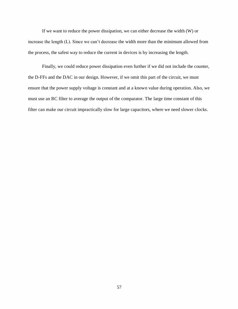
Figure 59 − Test results for capacitive water level sensing application
1, 112.25
0
100
200
300
400
500
600
700
800
900
1000
0 1 2 3 4 5 6 7 8
Cap
acit
an
ce (
in p
F)
Water Level (in cm)
linear Multimeter (pF) Sensing Circuit DAC
61
Table 10 summarizes the test results. Again, the formulas used to translate the output
voltages into capacitor values are Equations (5.5) and (5.6). From Figure 59, it is clear that
capacitance increases linearly with increasing water level. Hence, it is easy to “translate” the
measured capacitance to a specific water level value by using the following formula (blue line
indicates the ideal linear ratio between water level and capacitance):
𝑊𝑎𝑡𝑒𝑟 𝐿𝑒𝑣𝑒𝑙 (𝑐𝑚) =𝐶
112.25𝑝 (7.1)
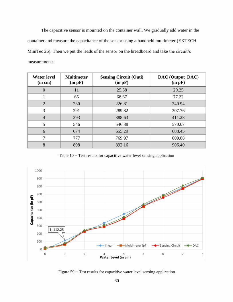
7.2 CAPACITIVE SOIL MOISTURE SENSOR
The second application of the sensing circuit is to measure the moisture content of soil in
relation to capacitance. For this application, we use the capacitive sensor presented previously in
the test setup shown in Figure 60.
Figure 60 −Test setup for capacitive soil moisture sensing
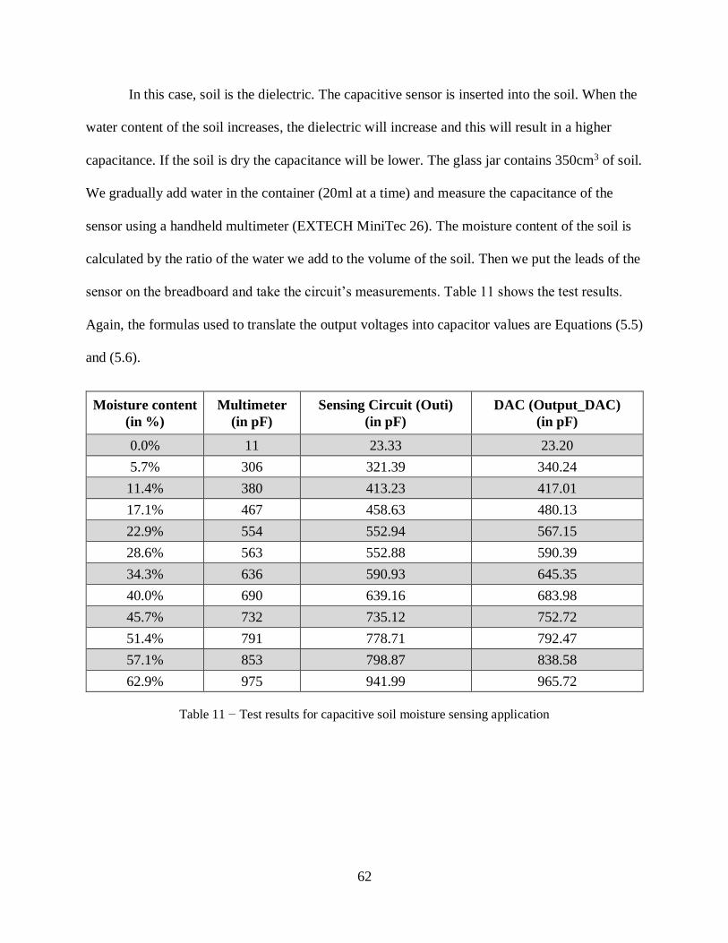
62
In this case, soil is the dielectric. The capacitive sensor is inserted into the soil. When the
water content of the soil increases, the dielectric will increase and this will result in a higher
capacitance. If the soil is dry the capacitance will be lower. The glass jar contains 350cm3 of soil.
We gradually add water in the container (20ml at a time) and measure the capacitance of the
sensor using a handheld multimeter (EXTECH MiniTec 26). The moisture content of the soil is
calculated by the ratio of the water we add to the volume of the soil. Then we put the leads of the
sensor on the breadboard and take the circuit’s measurements. Table 11 shows the test results.
Again, the formulas used to translate the output voltages into capacitor values are Equations (5.5)
and (5.6).
Moisture content
(in %)
Multimeter
(in pF)
Sensing Circuit (Outi)
(in pF)
DAC (Output_DAC)
(in pF)
0.0% 11 23.33 23.20
5.7% 306 321.39 340.24
11.4% 380 413.23 417.01
17.1% 467 458.63 480.13
22.9% 554 552.94 567.15
28.6% 563 552.88 590.39
34.3% 636 590.93 645.35
40.0% 690 639.16 683.98
45.7% 732 735.12 752.72
51.4% 791 778.71 792.47
57.1% 853 798.87 838.58
62.9% 975 941.99 965.72
Table 11 − Test results for capacitive soil moisture sensing application

63
Figure 61 − Test results for capacitive soil moisture sensing application
From Figure 61, it is clear that capacitance increases linearly with increasing moisture
content. Hence, it is easy to “translate” the measured capacitance to a specific moisture content
percentage by using the following formula (blue line indicates the ideal linear ratio between
moisture content and capacitance):
𝑀𝑜𝑖𝑠𝑡𝑢𝑟𝑒 𝐶𝑜𝑛𝑡𝑒𝑛𝑡 (%) =𝐶 − 306𝑝
1170.75𝑝+ 5.7 % (7.2)
7.3 APPLICATIONS DISCUSSION
In this Chapter, we used our design to measure water level and moisture content. As we
saw, the sensor we used has a capacitance that is linearly related to water level and moisture
content. Hence, it is easy to “translate” the measured capacitance (C) to the desired value by
5.7%, 306
0
100
200
300
400
500
600
700
800
900
1000
0% 5% 10% 15% 20% 25% 30% 35% 40% 45% 50% 55% 60% 65%
Cap
acit
ance
(in
pF)
Moisture Content (%)
Linear Multimeter Sensing Circuit DAC
64
using Equations (7.1) and (7.2). In the water level formula, 112.25p is the slope, and in the
moisture content formula, 306p is the capacitance measured for 5.7% moisture content and
1170.75 is the slope as shown in Figures 59 and 61.
The designed circuit and sensor could be used to measure the water level of liquids other
than water and moisture content for different types of soil. To do so, the system should be
calibrated first. For the first application, we should find the slope for the used liquid by taking
two capacitance values for two different water levels. For the second application, we can also
find the slope by taking two capacitance values for two different moisture contents, that we could
find using a moisture meter.
The PCB sensor is designed to measure liquid level up to 9 cm and average moisture
content of soil around this length. If we want to measure liquid level more than 9 cm the sensor
could be designed to be longer. It could also be designed to be less wide, so that its capacitance
per liquid cm would be less. If we would like to measure the moisture content of soil at a specific
depth, e.g. at the roots of a plant, sensor should be designed to be shorter. In general, the sensor
can be designed to fit the needs of the specific application.
The tested Integrated Circuit could be soldered on a battery powered PCB. The
“reference” and “bucket” capacitors would be soldered on the PCB, with capacitance values
based on the application. The sensor PCB could be connected to the chip’s PCB using wires
soldered on the respective pads. The outputs of the counter could be fed to a programmable
microcontroller which would be mounted on the same PCB and be programmed to give as output
the measured capacitance, or even “translate” this capacitance to water level or moisture content.
The output of the microcontroller could be seen on a LED display.

65
CHAPTER 8: CONCLUSION
This thesis set out to investigate how Delta-Sigma Modulation can be applied to
capacitive sensing. In this final chapter, we will review the contributions of this work and discuss
opportunities for future research.
The following are the main research contributions of this thesis:
• Design of a circuit that links linearly the ratio of a “test” to a “reference” capacitance to
the output of an analog-to-digital converter, using Delta-Sigma techniques (Chapter 2).
The equations governing the operation of this circuit were derived, the sub-circuits were
explained and their schematics and layouts were given.
• Fabrication of a chip using ON Semiconductor’s C5 process (Chapter 3). Capacitors and
clocks were not designed on-chip, so that the proposed circuit can be tested for a big
range of capacitors.
• Simulation of the designed circuit’s operation using Cadence Spectre Circuit Simulator
and prove its accuracy and linearity when testing capacitors in both pico-Farad and nano-
Farad range (Chapter 4). The immunity to power supply variations was simulated and the
linear relation between tested capacitance CTEST and power dissipation was shown.
• Test in the lab of the operation of the circuit for different capacitances and power supply
voltages and verification of the simulation results (Chapter 5). We also explained how
possible design mistakes can be addressed and new formulas were derived.
• Discuss of possible design variations that could make the proposed circuit more accurate,
faster, immune to design errors, more inclusive, take less layout area or dissipate less
power (Chapter 6). The trade-offs between possible implementations were discussed.

66
• Showcase of two possible Applications of the designed circuit: liquid level and moisture
content measurement (Chapter 7). The linear nature of the proposed design in
combination with the linear increase in sensor’s capacitance with liquid level or moisture
content made the “translation” between measured capacitance to the desired unit an easy
process.
The proposed design in this thesis has achieved its goal of sensing capacitances
accurately using Delta-Sigma Modulation and could be basis for future research. A circuit that is
insusceptible to process variations and allows the reference voltage to be at VDD/2 could be
designed, simulated and tested. Alternatively, methods for compensating the actual voltage
reference deviation from this desired value could be investigated. Furthermore, a more complete
design which will include a programmable microcontroller and will give output in the desired
unit for each specific application (i.e. cm for liquid level testing and percentage for moisture
content) could be tested. Finally, it could be researched the possibility of using the proposed
circuit or a modification of it for testing capacitances in the femto-Farad scale.
67
APPENDIX − SCHEMATICS AND LAYOUTS
• 2-input NAND

68
• 8-input NAND
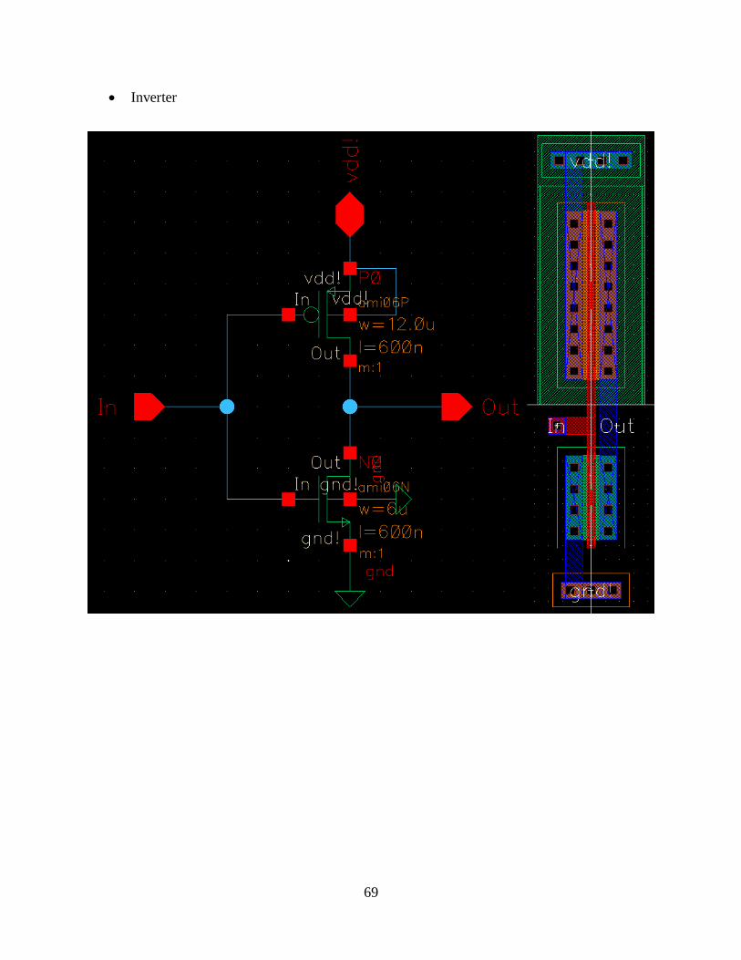
69
• Inverter

70
• 2-input NOR
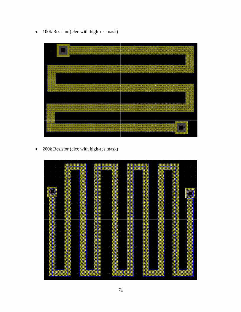
71
• 100k Resistor (elec with high-res mask)
• 200k Resistor (elec with high-res mask)
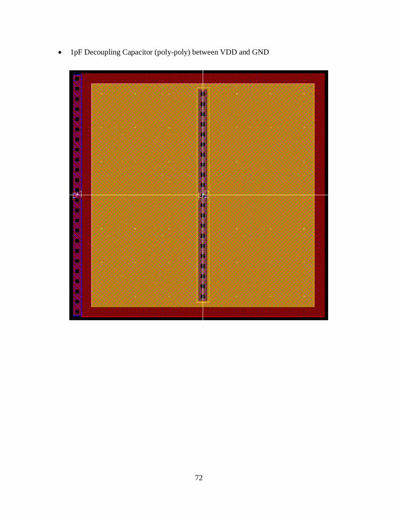
72
• 1pF Decoupling Capacitor (poly-poly) between VDD and GND
73
REFERENCES
[1] O'Dowd, J.; Callanan, A.; Banarie, G.; Company-Bosch, E., “Capacitive sensor
interfacing using sigma-delta techniques”, Sensors, 2005 IEEE, vol., no., pp.4 pp.-, Oct.
30 2005-Nov. 3 2005
[2] Ryan Seguine, Senior Product Manager, Cypress Semiconductor Corp., (2007,
November) “Capacitive Sensing Techniques and Considerations”, [Online], Available:
http://www.cypress.com/file/72986/download
[3] G. Nagy, Z. Szucs, S. Hodossy, M. Rencz, A. Poppe, “Comparison of Two Low-Power
Electronic Interfaces for Capacitive Mems Sensors”, Dans Symposium on Design, Test,
Integration and Packaging of MEMS/MOEMS - DTIP 2007, Stresa, lago Maggiore :
Italie (2007), arXiv:0802.3049
[4] R. Jacob Baker, CMOS Circuit Design, Layout and Simulation. Third Edition. Hoboken,
NJ: Wiley, 2010.
[5] H. Rapole, A. Rajagiri, M. Balasubramanian, K. A. Campbell and R. J. Baker,
“Resistive Memory Sensing Using Delta-Sigma Modulation,” 2009 IEEE Workshop on
Microelectronics and Electron Devices, Boise, ID, 2009, pp. 1-4.
[6] B. George, S. Agrawal and V. J. Kumar, “Switched - Capacitor Sigma - Delta
Capacitance to Digital Converter Suitable for Differential Capacitive Sensors,” 2007
IEEE Instrumentation & Measurement Technology Conference IMTC 2007, Warsaw,
2007, pp. 1-5.
74
[7] V. Saxena, T. J. Plum, J. R. Jessing and R. Jacob Baker, “Design and fabrication of a
MEMS capacitive chemical sensor system,” 2006 IEEE Workshop on Microelectronics
and Electron Devices, 2006. WMED '06, Boise, ID, 2006, pp. 2 pp.-18.
[8] “C5 Process: ON Semiconductor 0.50 μm,” MOSIS. [Online]. Available at:
https://www.mosis.com/vendors/view/on-semiconductor/c5. [Accessed: 2017].
[9] R. Jacob Baker, CMOS Mixed-Signal Circuit Design. Second Edition. Hoboken, NJ:
Wiley, 2009.
[10] Roberto La Rosa, "Using Active Circuits to Compensate For Resistance Variations In
Embedded Poly Resistors". U.S. Patent 7154325 B2, Dec. 26, 2006. Available at:
http://www.google.ch/patents/US7154325 [Accessed: 2017].
[11] “PCB as a Capacitive Soil Moisture Sensor”. [Online]. Available at:
http://zerocharactersleft.blogspot.com/2011/11/pcb-as-capacitive-soil-moisture-
sensor.html. [Accessed: 2017].
75
CURRICULUM VITAE
CHARIKLEIA TSAGKARI
Contact Information
Email: [email protected]
Education
University of Las Vegas, Nevada
MS, Electrical and Computer Engineering, May 2017
National Technical University of Athens, Greece
BS, Electrical and Computer Engineering, November 2009