design for reliability - welcome to the surface mount ... · pdf filecourse outline module 1:...
TRANSCRIPT
Design for Reliability
Greg Caswell, [email protected]
Senior Member of the Technical Staff
DfR Solutions
SMTA Boston June 3, 2015
Textron Facility
1
Abstract Designing printed boards and assemblies today is
more difficult than ever before because of the increased lead free process temperature requirements and associated changes required in manufacturing. Not only has the density of the electronic assembly increased, but many changes are taking place throughout the entire supply chain regarding the use of hazardous materials and the requirements for recycling.
Much of the change is due to the European Union (EU) Directives regarding these issues. The RoHS and REACH directives have caused many suppliers to the industry to rethink their materials and processes. Thus, everyone designing or producing electronics has been or will be affected.
2
Course Outline
MODULE 1: INTRODUCTIONS
Intro to Design for Reliability
DfR & Physics of Failure
MODULE 2: COMPONENTS
Selection
Critical Components
Moisture Sensitivity Level
Temperature Sensitivity Level
Electrostatic Discharge
Plating Material
Miscellaneous
Lifetime
Derating & Uprating
MODULE 3: MECHANISMS & PHYSICS
OF FAILURE
• Identifying Field Environment
• PoF Alternatives
• PoF Models & Examples
MODULE 4: PRINTED CIRCUIT BOARDS
• Surface Finishes
• Cracking & Delamination
• Laminate Selection
• Plated Through Vias (PTVs)
• PTH Barrel Cracking
• CAF
• Strain/Flexure Issues & Pad Cratering
• Cleanliness
• Electrochemical Migration
Nathan Myhrvold
“I want you to remember that everything
I am saying may be wrong and I want
you to question everything that I’m
saying.”
Module 1: Introduction to
DfR and Physics of Failure
(PoF)
Design for Reliability (DfR)
Defined
DfR: A process for ensuring the reliability of a
product or system during the design stage
before physical prototype
Reliability: The measure of a product’s ability
to
…perform the specified function
…at the customer (with their use environment)
…over the desired lifetime
Why Design for Reliability (DfR)?
The foundation of a reliable product is a robust design
Provides margin
Mitigates risk from defects
Satisfies the customer
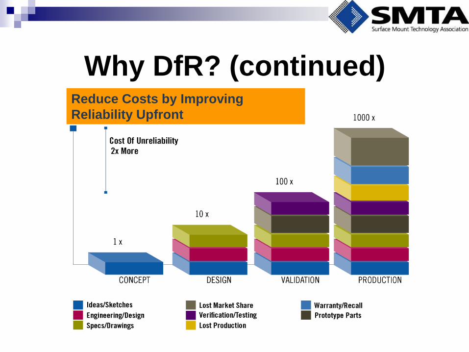
Why DfR? (continued) Reduce Costs by Improving
Reliability Upfront
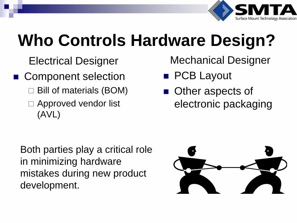
Who Controls Hardware Design? Electrical Designer
Component selection
Bill of materials (BOM)
Approved vendor list
(AVL)
Mechanical Designer
PCB Layout
Other aspects of
electronic packaging
Both parties play a critical role
in minimizing hardware
mistakes during new product
development.

When Do Mistakes Occur?
Insufficient exchange of information
between electrical design and mechanical
design
Poor understanding of supplier limitations
Customer expectations (reliability, lifetime,
use environment) are not incorporated into
the new product development (NPD)
process
“You don’t know what you don’t know”
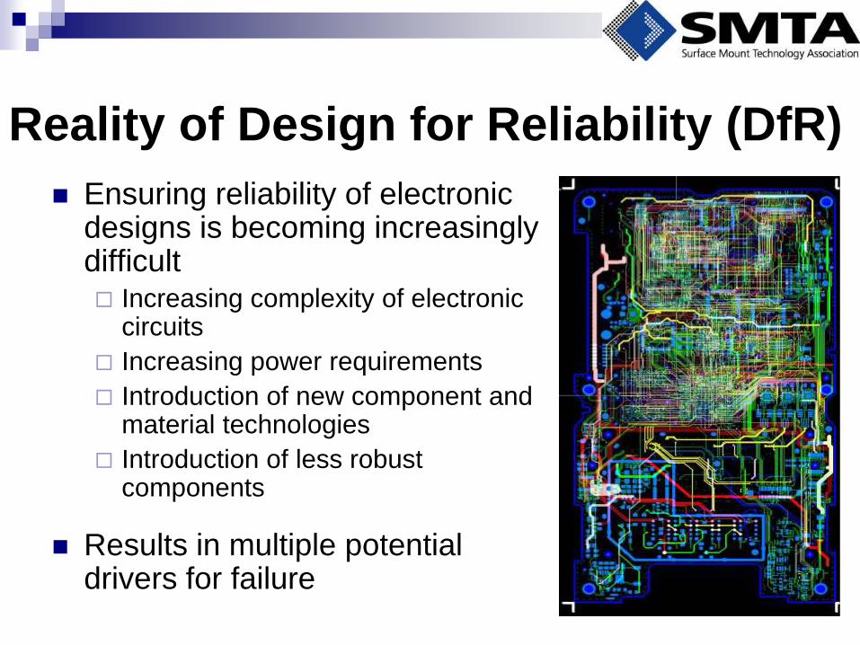
Reality of Design for Reliability (DfR)
Ensuring reliability of electronic designs is becoming increasingly difficult Increasing complexity of electronic
circuits
Increasing power requirements
Introduction of new component and material technologies
Introduction of less robust components
Results in multiple potential drivers for failure
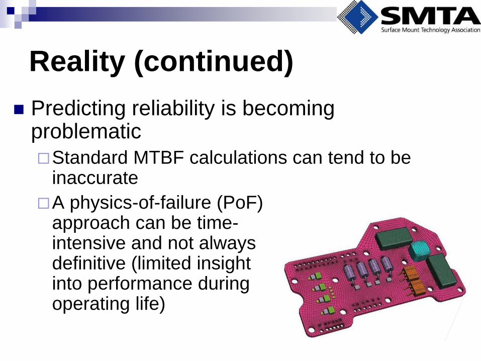
Reality (continued)
Predicting reliability is becoming problematic
Standard MTBF calculations can tend to be inaccurate
A physics-of-failure (PoF) approach can be time- intensive and not always definitive (limited insight into performance during operating life)
Limitations of Current DfR Too broad in focus: not electronics focused!
Too much emphasis on techniques (e.g., FMEA and FTA) and not answers FMEA/FTA rarely identify DfR issues because of limited focus on
the failure mechanism
Overreliance on MTBF calculations and standardized product testing
Incorporation of HALT and failure analysis (HALT is test, not DfR) is too late) Frustration with ‘test-in reliability’, even HALT, has been part of
the recent focus on DfR
DfR and Physics of Failure (PoF)
Due to some of the limitations of classic DfR, there has been an increasing interest in PoF (also known as: Reliability Physics)
PoF Definition: The use of science (physics, chemistry, etc.) to capture an understanding of failure mechanisms and evaluate useful life under actual operating conditions
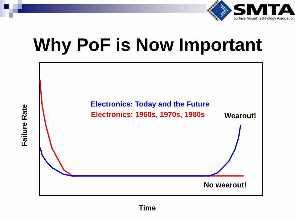
Why PoF is Now Important
Fail
ure
Rate
Time
Electronics: 1960s, 1970s, 1980s
No wearout!
Electronics: Today and the Future
Wearout!
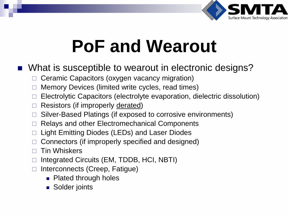
PoF and Wearout What is susceptible to wearout in electronic designs?
Ceramic Capacitors (oxygen vacancy migration)
Memory Devices (limited write cycles, read times)
Electrolytic Capacitors (electrolyte evaporation, dielectric dissolution)
Resistors (if improperly derated)
Silver-Based Platings (if exposed to corrosive environments)
Relays and other Electromechanical Components
Light Emitting Diodes (LEDs) and Laser Diodes
Connectors (if improperly specified and designed)
Tin Whiskers
Integrated Circuits (EM, TDDB, HCI, NBTI)
Interconnects (Creep, Fatigue)
Plated through holes
Solder joints
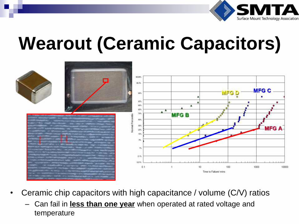
• Ceramic chip capacitors with high capacitance / volume (C/V) ratios
– Can fail in less than one year when operated at rated voltage and
temperature
Wearout (Ceramic Capacitors)
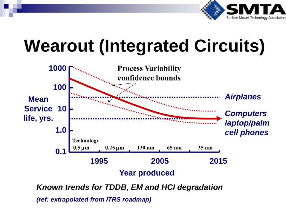
Wearout (Integrated Circuits)
1995 2005 2015
0.1
1.0
10
100
1000
Year produced
Known trends for TDDB, EM and HCI degradation
(ref: extrapolated from ITRS roadmap)
Mean
Service
life, yrs. Computers
laptop/palm
cell phones
Airplanes
0.5 mm 0.25 mm 130 nm 65 nm 35 nm
Process Variability
confidence bounds
Technology
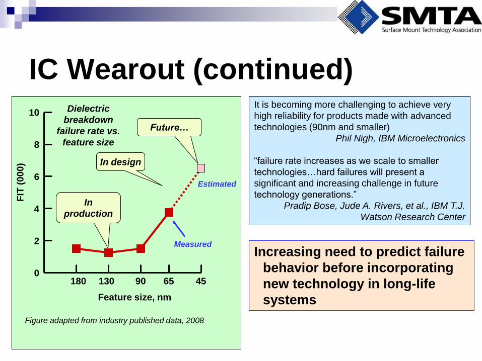
IC Wearout (continued)
180 130 90 65 45 0
2
4
6
8
10
FIT
(0
00
)
Feature size, nm
It is becoming more challenging to achieve very
high reliability for products made with advanced
technologies (90nm and smaller)
Phil Nigh, IBM Microelectronics
“failure rate increases as we scale to smaller
technologies…hard failures will present a
significant and increasing challenge in future
technology generations.”
Pradip Bose, Jude A. Rivers, et al., IBM T.J.
Watson Research Center
Figure adapted from industry published data, 2008
In
production
Future…
In design
Dielectric
breakdown
failure rate vs.
feature size
Estimated
Measured Increasing need to predict failure
behavior before incorporating
new technology in long-life
systems
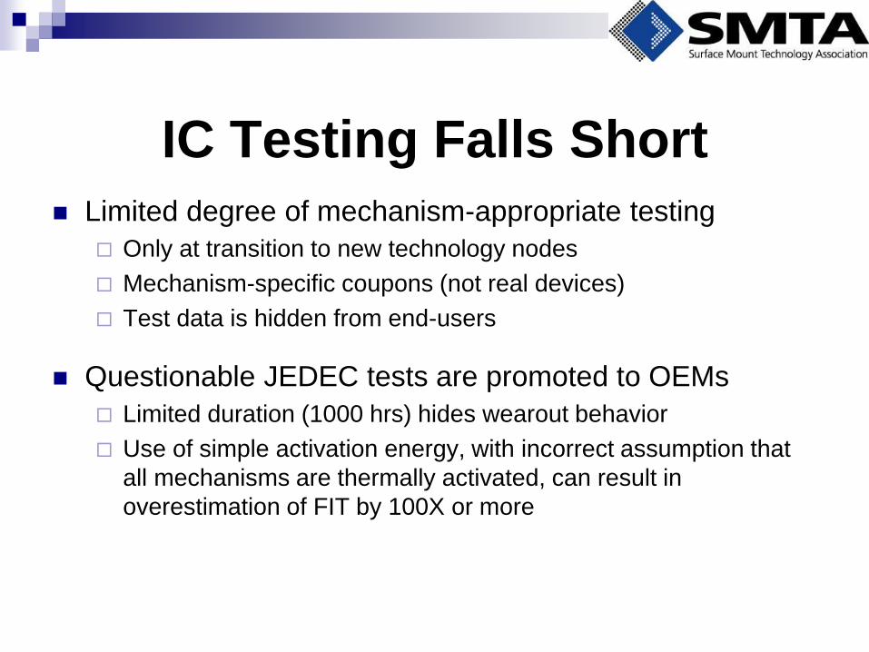
IC Testing Falls Short
Limited degree of mechanism-appropriate testing
Only at transition to new technology nodes
Mechanism-specific coupons (not real devices)
Test data is hidden from end-users
Questionable JEDEC tests are promoted to OEMs
Limited duration (1000 hrs) hides wearout behavior
Use of simple activation energy, with incorrect assumption that
all mechanisms are thermally activated, can result in
overestimation of FIT by 100X or more
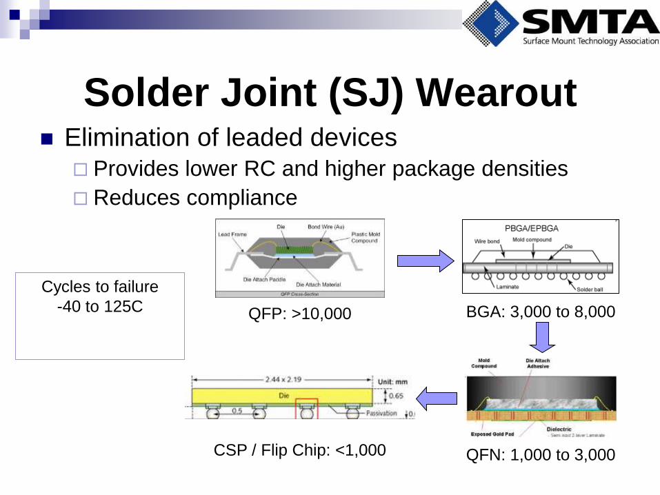
Solder Joint (SJ) Wearout Elimination of leaded devices
Provides lower RC and higher package densities
Reduces compliance
Cycles to failure
-40 to 125C QFP: >10,000 BGA: 3,000 to 8,000
QFN: 1,000 to 3,000 CSP / Flip Chip: <1,000
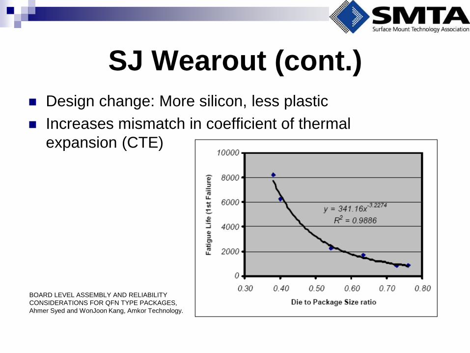
SJ Wearout (cont.)
Design change: More silicon, less plastic
Increases mismatch in coefficient of thermal
expansion (CTE)
BOARD LEVEL ASSEMBLY AND RELIABILITY
CONSIDERATIONS FOR QFN TYPE PACKAGES,
Ahmer Syed and WonJoon Kang, Amkor Technology.
Industry Testing of SJ Wearout
JEDEC
Specification body for component manufacturers
JEDEC JESD4747H, February 2011
Guidelines for new component qualification
Requires 2300 cycles of 0 to 100C
Testing is often done on thin boards
IPC
Specification body for electronic OEMs
IPC 9701A, February 2006
Recommends 6000 cycles of 0 to 100C
Test boards should be similar thickness as actual design
Implementing DfR / PoF
Many organizations have developed DfR Teams to speed implementation
Success is dependent upon team composition and gating functions
Challenges: Classic design teams consist of electrical and mechanical engineers trained in the ‘science of success’
PoF requires the right elements of personnel and tools
DfR / PoF Team Component engineer
Mechanical / Materials engineer
Electrical engineer
Thermal engineer Depending upon power requirements
Reliability engineer? Depends. Many classic reliability engineers
provide NO value in the DfR / PoF process due to over-emphasis on statistical techniques and environmental testing
Module 2: Components
Component Selection
The process of creating the bill of
materials (BOM) during the ‘virtual’ design
process
Before physical layout
For some companies, this is during the
creation of the approved vendor list (AVL)
Design-independent
Component Selection (continued)
As technology progresses, functional performance has
become a limited aspect of the part selection process
Other concerns are increasingly taking center stage
Moisture sensitivity level (MSL)
Temperature sensitivity level
Electrostatic discharge (ESD) classification
Manufacturability (Design for Assembly)
Plating material
Lifetime / Long-term reliability
Sometimes Physics of Failure is required
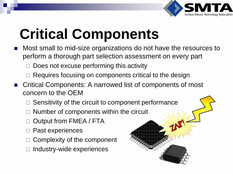
Critical Components Most small to mid-size organizations do not have the resources to
perform a thorough part selection assessment on every part
Does not excuse performing this activity
Requires focusing on components critical to the design
Critical Components: A narrowed list of components of most
concern to the OEM
Sensitivity of the circuit to component performance
Number of components within the circuit
Output from FMEA / FTA
Past experiences
Complexity of the component
Industry-wide experiences
Critical Components (Industry Experience)
Optoelectronics High volume controls not always in place
Wearout can initiate far before 20 years
Low volume or custom parts Part is no longer a commodity item
Memory devices Non-volatile memory has limited data retention time and
write cycles
Parts with mechanical movements (switches, relays, potentiostats, fans) Depending on environment, wear out can initiate far before 20
years
Surface mount ceramic capacitors Assembly issues
Critical Components (continued)
New technologies or state-of-the-art At the limit of the manufacturer’s capabilities
MEMS, 45-nm technology, green materials, etc.
Electronic modules Part is a miniature assembly (no longer a commodity item)
Power components
Fuses Susceptible to quality issues
Electrolytic capacitors Depending on environment, wear out can initiate far before
20 years
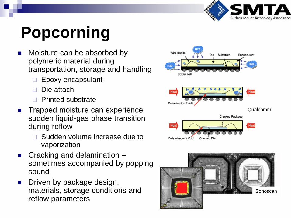
Popcorning Moisture can be absorbed by
polymeric material during transportation, storage and handling
Epoxy encapsulant
Die attach
Printed substrate
Trapped moisture can experience sudden liquid-gas phase transition during reflow
Sudden volume increase due to vaporization
Cracking and delamination – sometimes accompanied by popping sound
Driven by package design, materials, storage conditions and reflow parameters
Qualcomm
Sonoscan

MSL Issues and Actions (continued)
Most ‘standard’ components have a maximum MSL 3
Components with MSL 4 and higher
Large ball grid array (BGA) packages
Encapsulated magnetic components (chokes, transformers, etc.)
Optical components (transmitters, transceivers, sensors, etc.)
Modules (DC-DC converters, GPS, etc.)
MSL classification scheme in J-STD-020D is only relevant to SMT packages with integrated circuits
Does not cover passives (IPC-9503) or wave soldering (JESD22A111)
If not defined by component manufacturer, requires additional characterization
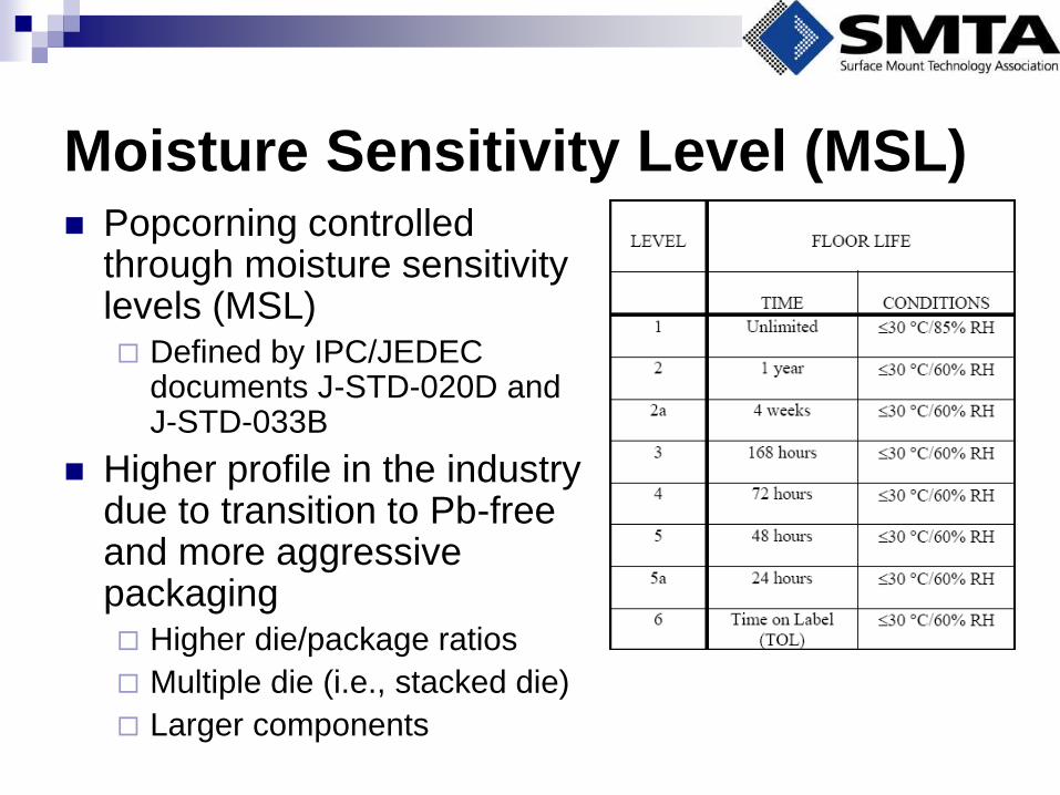
Moisture Sensitivity Level (MSL) Popcorning controlled
through moisture sensitivity levels (MSL) Defined by IPC/JEDEC
documents J-STD-020D and J-STD-033B
Higher profile in the industry due to transition to Pb-free and more aggressive packaging Higher die/package ratios
Multiple die (i.e., stacked die)
Larger components

MSL: Typical Issues and Action
Items Identify your maximum MSL
Driven by contract manufacturer (CM) capability and OEM risk aversion
Majority limit between MSL3 and MSL4 (survey of the MSD Council of SMTA, 2004)
High volume, low mix: tends towards MSL4 Low volume, high mix: tends towards MSL3
Not all datasheets list MSL Can be buried in reference or quality documents
Ensure that listed MSL conforms to latest version of J-STD-020
Cogiscan
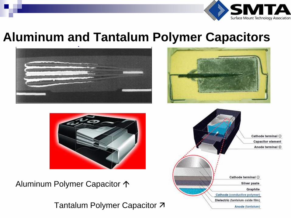
Aluminum and Tantalum Polymer Capacitors
Aluminum Polymer Capacitor
Tantalum Polymer Capacitor
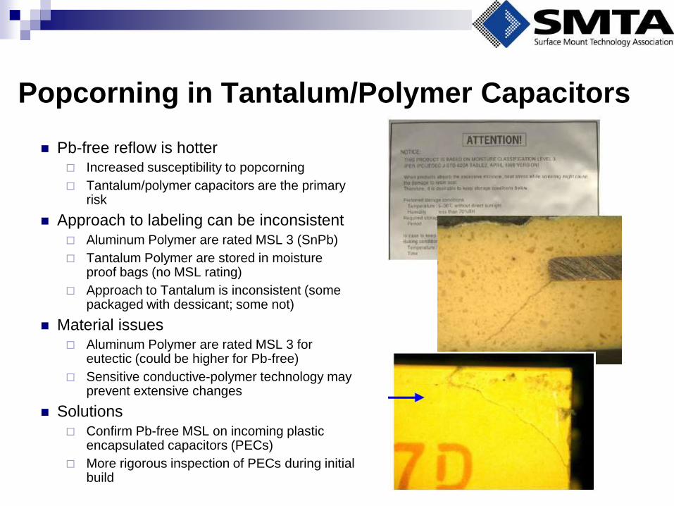
Popcorning in Tantalum/Polymer Capacitors
Pb-free reflow is hotter Increased susceptibility to popcorning
Tantalum/polymer capacitors are the primary risk
Approach to labeling can be inconsistent
Aluminum Polymer are rated MSL 3 (SnPb)
Tantalum Polymer are stored in moisture proof bags (no MSL rating)
Approach to Tantalum is inconsistent (some packaged with dessicant; some not)
Material issues Aluminum Polymer are rated MSL 3 for
eutectic (could be higher for Pb-free)
Sensitive conductive-polymer technology may prevent extensive changes
Solutions
Confirm Pb-free MSL on incoming plastic encapsulated capacitors (PECs)
More rigorous inspection of PECs during initial build
Temperature Sensitivity
Limits on process temperatures provided by component
manufacturer
Components of concern with SnPb (220C peak) included RF devices and
some optoelectronic components
Broader issue due to introduction of Pb-free processes (260C
peak)
Initially limited: SnPb reflow sensitive components, SMT connectors,
ceramic capacitors, SMT
electrolytic capacitors
Primary issue for some OEMs
Current component packaging
technology is insufficiently robust
Numerous components in a telecom /
enterprise design now have peak
temperatures below 260C

Component Selection for ESD
Industry movement to decreasing feature
sizes and high frequency technology
90nm 65nm 45nm
GaAs / SiGe desirable at high GHz
Increasing ESD risks
More parts are ESD susceptible
ESD sensitivity is increasing (is Class 0 still
sufficient?)
Design for ESD Prevention:
What Do You Need to Do?
ESD Protection is necessary at the IC, component
package and system level
Different approaches are needed to achieve reliable
protection
Designing for ESD impacts both the product design and
the manufacturing process controls
What technologies are available to assure a reliable ESD
protected product?
At the IC level
At the component package level
At the system level
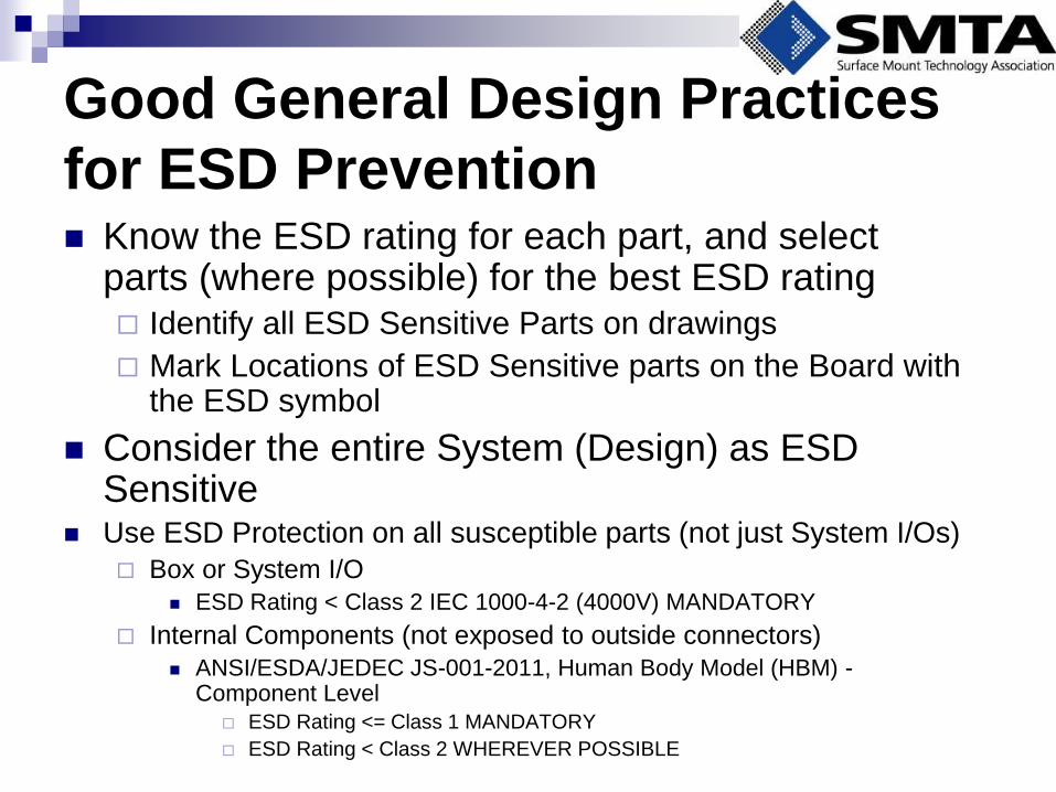
Good General Design Practices
for ESD Prevention Know the ESD rating for each part, and select
parts (where possible) for the best ESD rating Identify all ESD Sensitive Parts on drawings
Mark Locations of ESD Sensitive parts on the Board with the ESD symbol
Consider the entire System (Design) as ESD Sensitive
Use ESD Protection on all susceptible parts (not just System I/Os)
Box or System I/O
ESD Rating < Class 2 IEC 1000-4-2 (4000V) MANDATORY
Internal Components (not exposed to outside connectors)
ANSI/ESDA/JEDEC JS-001-2011, Human Body Model (HBM) - Component Level
ESD Rating <= Class 1 MANDATORY
ESD Rating < Class 2 WHEREVER POSSIBLE
DfR and Tin Whiskers
The first step is to focus DfR on critical components
Critical components are based upon three pieces of knowledge
The overwhelming majority of tin-plated electronic parts are matte tin over copper
Matte tin over copper produces whiskers of a finite length
Whiskers tend to only break off during handling
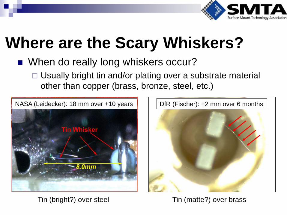
Where are the Scary Whiskers? When do really long whiskers occur?
Usually bright tin and/or plating over a substrate material
other than copper (brass, bronze, steel, etc.)
NASA (Leidecker): 18 mm over +10 years DfR (Fischer): +2 mm over 6 months
Tin (bright?) over steel Tin (matte?) over brass
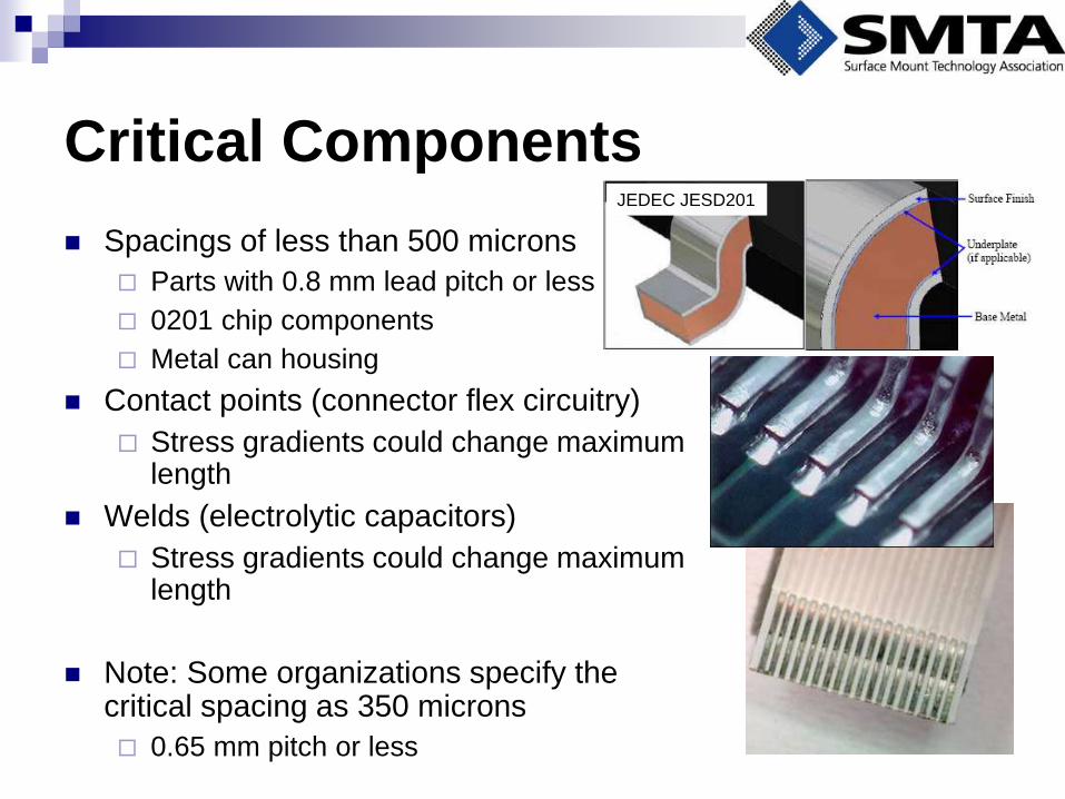
Critical Components
Spacings of less than 500 microns
Parts with 0.8 mm lead pitch or less
0201 chip components
Metal can housing
Contact points (connector flex circuitry)
Stress gradients could change maximum length
Welds (electrolytic capacitors)
Stress gradients could change maximum length
Note: Some organizations specify the critical spacing as 350 microns
0.65 mm pitch or less
JEDEC JESD201
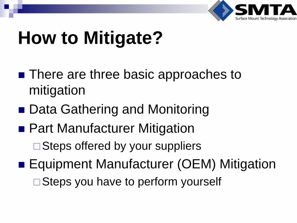
How to Mitigate?
There are three basic approaches to
mitigation
Data Gathering and Monitoring
Part Manufacturer Mitigation
Steps offered by your suppliers
Equipment Manufacturer (OEM) Mitigation
Steps you have to perform yourself
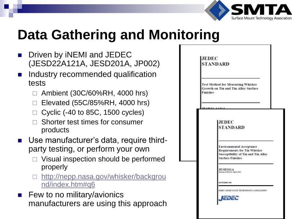
Data Gathering and Monitoring
Driven by iNEMI and JEDEC (JESD22A121A, JESD201A, JP002)
Industry recommended qualification tests
Ambient (30C/60%RH, 4000 hrs)
Elevated (55C/85%RH, 4000 hrs)
Cyclic (-40 to 85C, 1500 cycles)
Shorter test times for consumer products
Use manufacturer’s data, require third-party testing, or perform your own
Visual inspection should be performed properly
http://nepp.nasa.gov/whisker/background/index.htm#q6
Few to no military/avionics manufacturers are using this approach
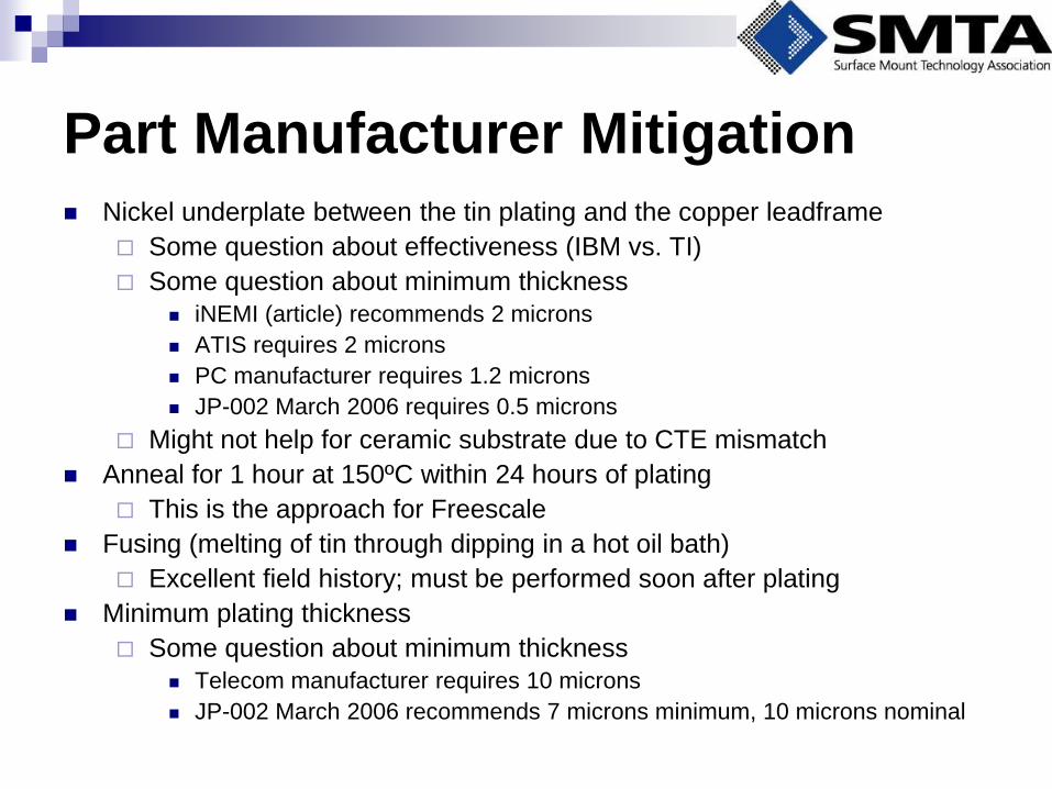
Part Manufacturer Mitigation Nickel underplate between the tin plating and the copper leadframe
Some question about effectiveness (IBM vs. TI)
Some question about minimum thickness
iNEMI (article) recommends 2 microns
ATIS requires 2 microns
PC manufacturer requires 1.2 microns
JP-002 March 2006 requires 0.5 microns
Might not help for ceramic substrate due to CTE mismatch
Anneal for 1 hour at 150ºC within 24 hours of plating
This is the approach for Freescale
Fusing (melting of tin through dipping in a hot oil bath)
Excellent field history; must be performed soon after plating
Minimum plating thickness
Some question about minimum thickness
Telecom manufacturer requires 10 microns
JP-002 March 2006 recommends 7 microns minimum, 10 microns nominal
Part Manufacturer Mitigation (continued)
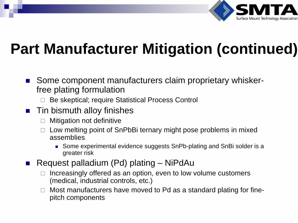
Some component manufacturers claim proprietary whisker-free plating formulation Be skeptical; require Statistical Process Control
Tin bismuth alloy finishes Mitigation not definitive
Low melting point of SnPbBi ternary might pose problems in mixed assemblies
Some experimental evidence suggests SnPb-plating and SnBi solder is a greater risk
Request palladium (Pd) plating – NiPdAu Increasingly offered as an option, even to low volume customers
(medical, industrial controls, etc.)
Most manufacturers have moved to Pd as a standard plating for fine-pitch components
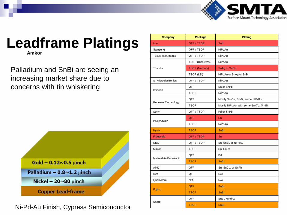
Leadframe Platings Amkor
Palladium and SnBi are seeing an
increasing market share due to
concerns with tin whiskering
Company Package Plating
Intel QFP / TSOP Sn[1]
Samsung QFP / TSOP NiPdAu
Texas Instruments QFP / TSOP NiPdAu
Toshiba
TSOP (Discretes) NiPdAu
TSOP (Memory) SnAg or SnCu
TSOP (LSI) NiPdAu or SnAg or SnBi
STMicroelectronics QFP / TSOP NiPdAu
Infineon QFP Sn or SnPb
TSOP NiPdAu
Renesas Technology QFP Mostly Sn-Cu, Sn-Bi; some NiPdAu
TSOP Mostly NiPdAu, with some Sn-Cu, Sn-Bi
Sony QFP / TSOP Pd or SnPb
Philips/NXP QFP Sn
TSOP NiPdAu
Hynix TSOP SnBi
Freescale QFP / TSOP Sn
NEC QFP / TSOP Sn, SnBi, or NiPdAu
Micron TSOP Sn, SnPb
Matsushita/Panasonic QFP Pd
TSOP SnBi
AMD QFP Sn, SnCu, or SnPb
IBM QFP N/A
Qualcomm N/A N/A
Fujitsu QFP SnBi
TSOP SnBi
Sharp QFP SnBi, NiPdAu
TSOP SnBi
Ni-Pd-Au Finish, Cypress Semiconductor
OEM Mitigation
Four Options
Procurement, Re-packaging, Post-plate or dip, Conformal
coat
Procurement / Design
Select only components with SnPb or Pd plating
May require complete change in circuit design if alternative
component required
Rarely performed (functionality trumps reliability)
Subcontract packaging or Re-packaging
SnPb or Pd plated leadframes
Rarely performed (cost, risk of damage)
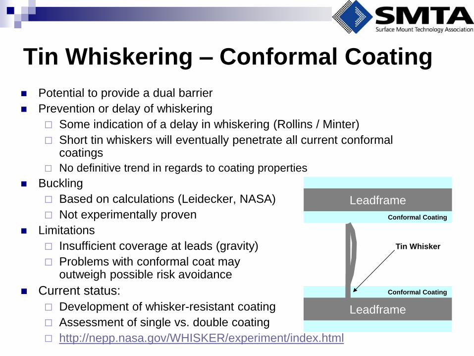
Tin Whiskering – Conformal Coating
Potential to provide a dual barrier
Prevention or delay of whiskering
Some indication of a delay in whiskering (Rollins / Minter)
Short tin whiskers will eventually penetrate all current conformal coatings
No definitive trend in regards to coating properties
Buckling
Based on calculations (Leidecker, NASA)
Not experimentally proven
Limitations
Insufficient coverage at leads (gravity)
Problems with conformal coat may outweigh possible risk avoidance
Current status:
Development of whisker-resistant coating
Assessment of single vs. double coating
http://nepp.nasa.gov/WHISKER/experiment/index.html
Leadframe
Conformal Coating
Leadframe
Conformal Coating
Tin Whisker
Mitigation efforts can fail when only one
source of stress is accounted for.
For example if a Ni layer is used to
prevent stress from IMC formation, this will
not address whisker formation due to
corrosion or external pressure.
All the potential sources of stress for a
particular application should be considered
in the mitigation process.
A New Approach to Mitigation
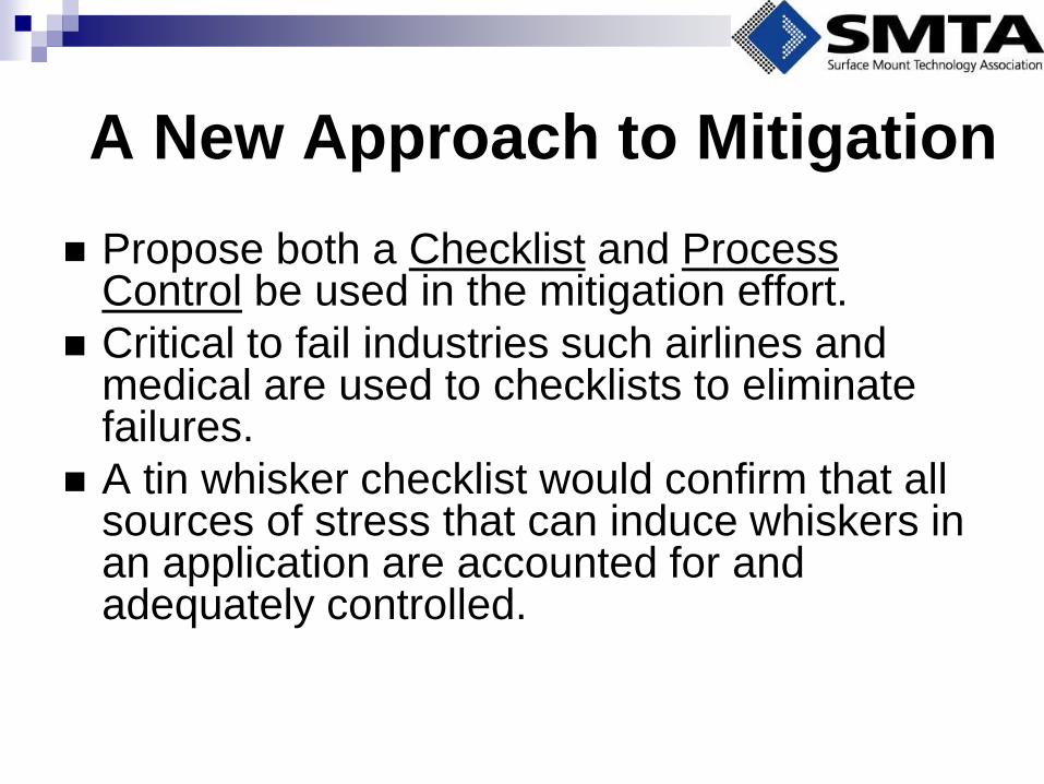
Propose both a Checklist and Process Control be used in the mitigation effort.
Critical to fail industries such airlines and medical are used to checklists to eliminate failures.
A tin whisker checklist would confirm that all sources of stress that can induce whiskers in an application are accounted for and adequately controlled.
A New Approach to Mitigation
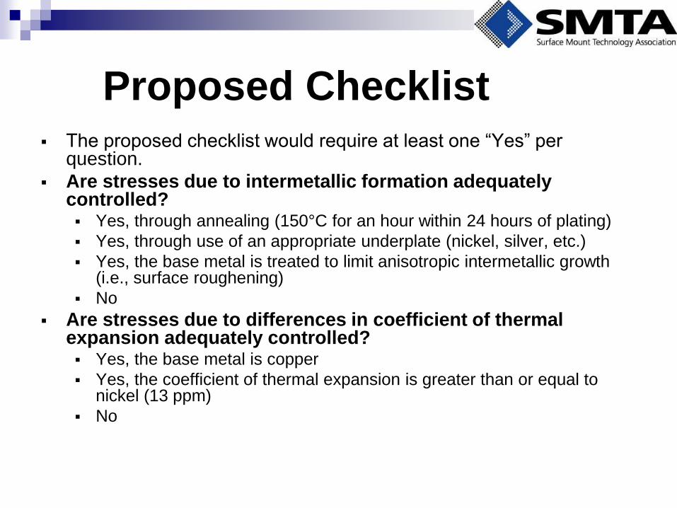
The proposed checklist would require at least one “Yes” per question.
Are stresses due to intermetallic formation adequately controlled? Yes, through annealing (150°C for an hour within 24 hours of plating)
Yes, through use of an appropriate underplate (nickel, silver, etc.)
Yes, the base metal is treated to limit anisotropic intermetallic growth (i.e., surface roughening)
No
Are stresses due to differences in coefficient of thermal expansion adequately controlled? Yes, the base metal is copper
Yes, the coefficient of thermal expansion is greater than or equal to nickel (13 ppm)
No
Proposed Checklist
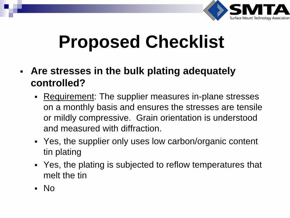
Are stresses in the bulk plating adequately
controlled?
Requirement: The supplier measures in-plane stresses
on a monthly basis and ensures the stresses are tensile
or mildly compressive. Grain orientation is understood
and measured with diffraction.
Yes, the supplier only uses low carbon/organic content
tin plating
Yes, the plating is subjected to reflow temperatures that
melt the tin
No
Proposed Checklist
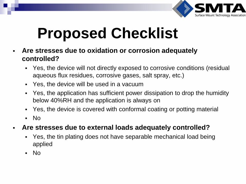
Are stresses due to oxidation or corrosion adequately
controlled?
Yes, the device will not directly exposed to corrosive conditions (residual
aqueous flux residues, corrosive gases, salt spray, etc.)
Yes, the device will be used in a vacuum
Yes, the application has sufficient power dissipation to drop the humidity
below 40%RH and the application is always on
Yes, the device is covered with conformal coating or potting material
No
Are stresses due to external loads adequately controlled?
Yes, the tin plating does not have separable mechanical load being
applied
No
Proposed Checklist
Component Selection
(Misc)

Ceramic Capacitors (Cyclic Voltage)
Reports of field failures of MLCC in AC or pulsed DC voltage
Piezoelectric effect Variant voltage will vary internal
stresses, potentially inducing fatigue behavior
With high frequency ripple current, capacitor can vibrate (resonate).
Fatigued specimens can contain scattered microcracks Decrease in capacitance;
increase in leakage current
Concern at hundreds of kHz Decreases with increasing
capacitance, X7R -> Y5V
Avoid or use AC-rated capacitors
Sang-Joo Kim and Qing Jiangy, Microcracking and electric fatigue of
polycrystalline ferroelectric ceramics, Smart Mater. Struct. 5 (1996)
English Metric
3025 7563 250 - 750 kHz
2220 5750 300 - 900 kHz
1812 4532 400 - 1200 kHz
1210 3225 600 - 1200 kHz
1206 3216 600 - 1600 kHz
0805 2012 900 - 1800 kHz
0603 1608 N/A
0402 1005 N/A
Case SizeResonance Frequency
Nippon Chemi-con, CAT.No.E1002l
http://www.avxcorp.com/docs/techinfo/parasitc.pdf
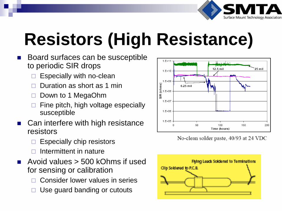
Resistors (High Resistance) Board surfaces can be susceptible
to periodic SIR drops
Especially with no-clean
Duration as short as 1 min
Down to 1 MegaOhm
Fine pitch, high voltage especially susceptible
Can interfere with high resistance resistors
Especially chip resistors
Intermittent in nature
Avoid values > 500 kOhms if used for sensing or calibration
Consider lower values in series
Use guard banding or cutouts
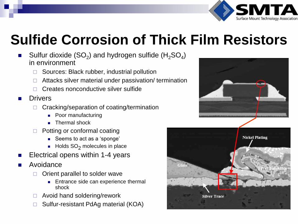
Sulfide Corrosion of Thick Film Resistors Sulfur dioxide (SO2) and hydrogen sulfide (H2SO4)
in environment
Sources: Black rubber, industrial pollution
Attacks silver material under passivation/ termination
Creates nonconductive silver sulfide
Drivers
Cracking/separation of coating/termination
Poor manufacturing
Thermal shock
Potting or conformal coating
Seems to act as a ‘sponge’
Holds SO2 molecules in place
Electrical opens within 1-4 years
Avoidance
Orient parallel to solder wave
Entrance side can experience thermal shock
Avoid hand soldering/rework
Sulfur-resistant PdAg material (KOA)
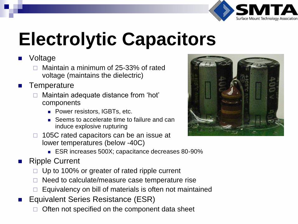
Electrolytic Capacitors Voltage
Maintain a minimum of 25-33% of rated voltage (maintains the dielectric)
Temperature
Maintain adequate distance from ‘hot’ components
Power resistors, IGBTs, etc.
Seems to accelerate time to failure and can induce explosive rupturing
105C rated capacitors can be an issue at lower temperatures (below -40C)
ESR increases 500X; capacitance decreases 80-90%
Ripple Current
Up to 100% or greater of rated ripple current
Need to calculate/measure case temperature rise
Equivalency on bill of materials is often not maintained
Equivalent Series Resistance (ESR)
Often not specified on the component data sheet
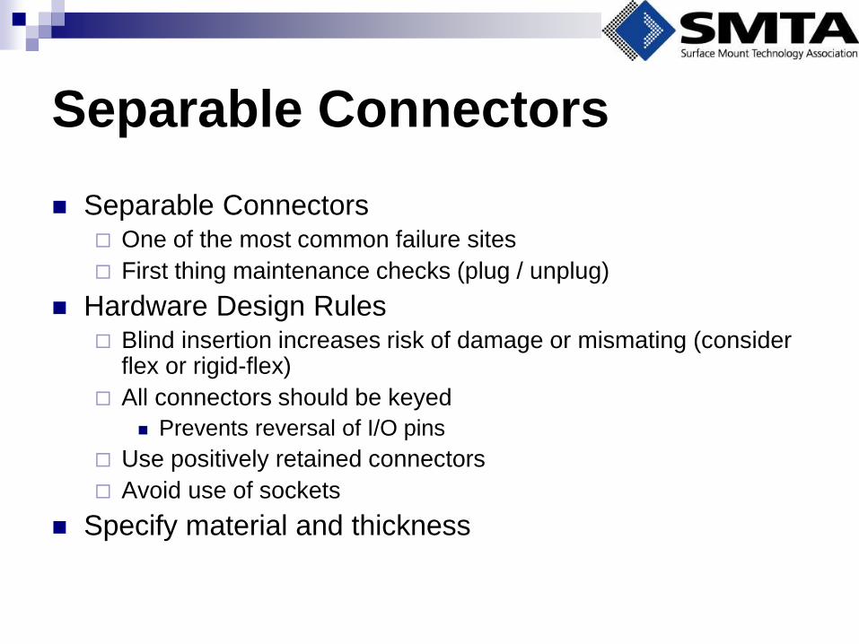
Separable Connectors
Separable Connectors One of the most common failure sites
First thing maintenance checks (plug / unplug)
Hardware Design Rules Blind insertion increases risk of damage or mismating (consider
flex or rigid-flex)
All connectors should be keyed
Prevents reversal of I/O pins
Use positively retained connectors
Avoid use of sockets
Specify material and thickness
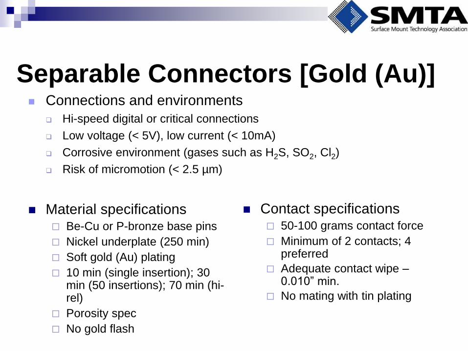
Separable Connectors [Gold (Au)]
Material specifications Be-Cu or P-bronze base pins
Nickel underplate (250 min)
Soft gold (Au) plating
10 min (single insertion); 30 min (50 insertions); 70 min (hi-rel)
Porosity spec
No gold flash
Contact specifications 50-100 grams contact force
Minimum of 2 contacts; 4 preferred
Adequate contact wipe – 0.010” min.
No mating with tin plating
Connections and environments
Hi-speed digital or critical connections
Low voltage (< 5V), low current (< 10mA)
Corrosive environment (gases such as H2S, SO2, Cl2)
Risk of micromotion (< 2.5 µm)
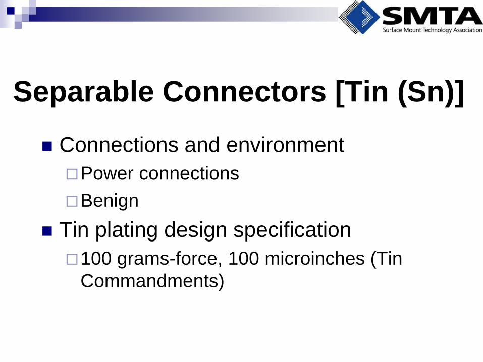
Separable Connectors [Tin (Sn)]
Connections and environment
Power connections
Benign
Tin plating design specification
100 grams-force, 100 microinches (Tin
Commandments)
Component Selection
(Lifetime)
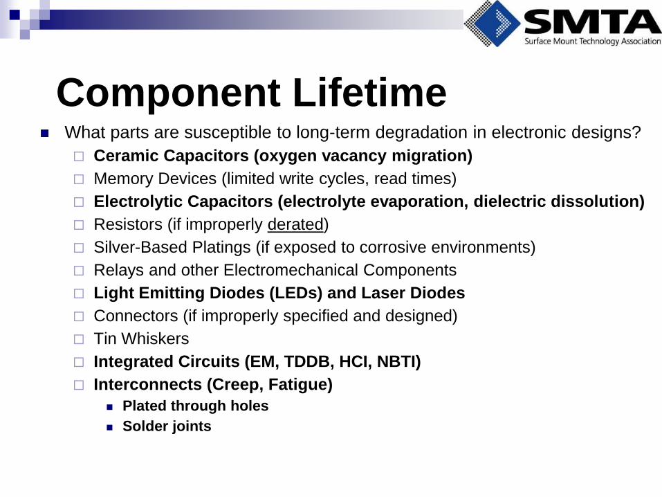
Component Lifetime What parts are susceptible to long-term degradation in electronic designs?
Ceramic Capacitors (oxygen vacancy migration)
Memory Devices (limited write cycles, read times)
Electrolytic Capacitors (electrolyte evaporation, dielectric dissolution)
Resistors (if improperly derated)
Silver-Based Platings (if exposed to corrosive environments)
Relays and other Electromechanical Components
Light Emitting Diodes (LEDs) and Laser Diodes
Connectors (if improperly specified and designed)
Tin Whiskers
Integrated Circuits (EM, TDDB, HCI, NBTI)
Interconnects (Creep, Fatigue)
Plated through holes
Solder joints
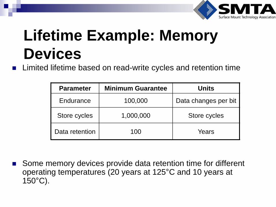
Lifetime Example: Memory
Devices
Parameter Minimum Guarantee Units
Endurance 100,000 Data changes per bit
Store cycles 1,000,000 Store cycles
Data retention 100 Years
Limited lifetime based on read-write cycles and retention time
Some memory devices provide data retention time for different operating temperatures (20 years at 125°C and 10 years at 150°C).
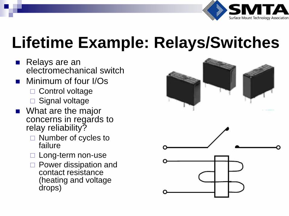
Lifetime Example: Relays/Switches Relays are an
electromechanical switch
Minimum of four I/Os Control voltage
Signal voltage
What are the major concerns in regards to relay reliability? Number of cycles to
failure
Long-term non-use
Power dissipation and contact resistance (heating and voltage drops)
Relays/Switches (continued)
Selection of appropriate plating
Idle for long periods of time: Gold contacts
Numerous cycles: AgCd contacts
Sealed packages if cleaning operations
Use of protective devices
Diode, resistor, capacitor, varistor, etc.
Prevents arcing during switching (accelerates degradation)
Must be nearby
Temperature rise
Wide range of contact resistance in specifications
Ensure margin between design life requirements and manufacturer’s specifications

0%
10%
20%
30%
40%
50%
60%
70%
80%
90%
100%
60,000 70,000 80,000 90,000 100,000 110,000 120,000 130,000
Number of Cycles
Cu
mu
lati
ve F
ail
ure
s %
Characteristic
Life = 113,545
Catalog Life =
100,000 CyclesMean Time Between
Failures = 102,900
Wearout of Relays/Switches
Derating and Uprating
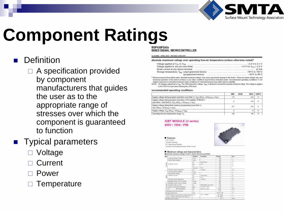
Component Ratings
Definition
A specification provided by component manufacturers that guides the user as to the appropriate range of stresses over which the component is guaranteed to function
Typical parameters
Voltage
Current
Power
Temperature
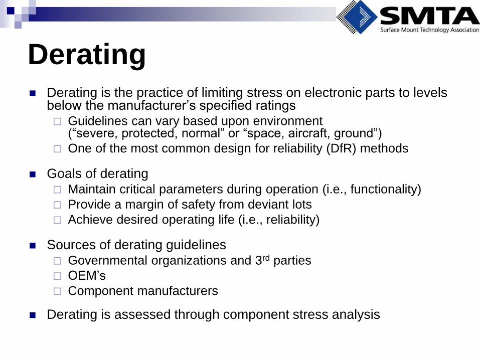
Derating Derating is the practice of limiting stress on electronic parts to levels
below the manufacturer’s specified ratings Guidelines can vary based upon environment
(“severe, protected, normal” or “space, aircraft, ground”)
One of the most common design for reliability (DfR) methods
Goals of derating Maintain critical parameters during operation (i.e., functionality)
Provide a margin of safety from deviant lots
Achieve desired operating life (i.e., reliability)
Sources of derating guidelines Governmental organizations and 3rd parties
OEM’s
Component manufacturers
Derating is assessed through component stress analysis
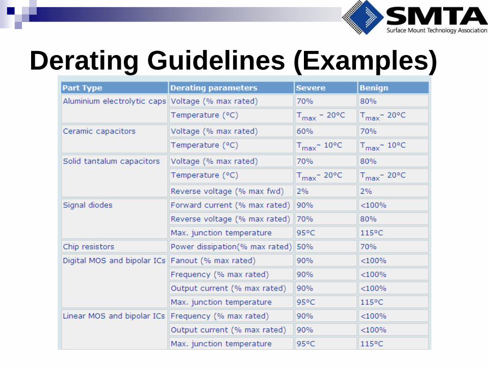
Derating Guidelines (Examples)
Derating Failures
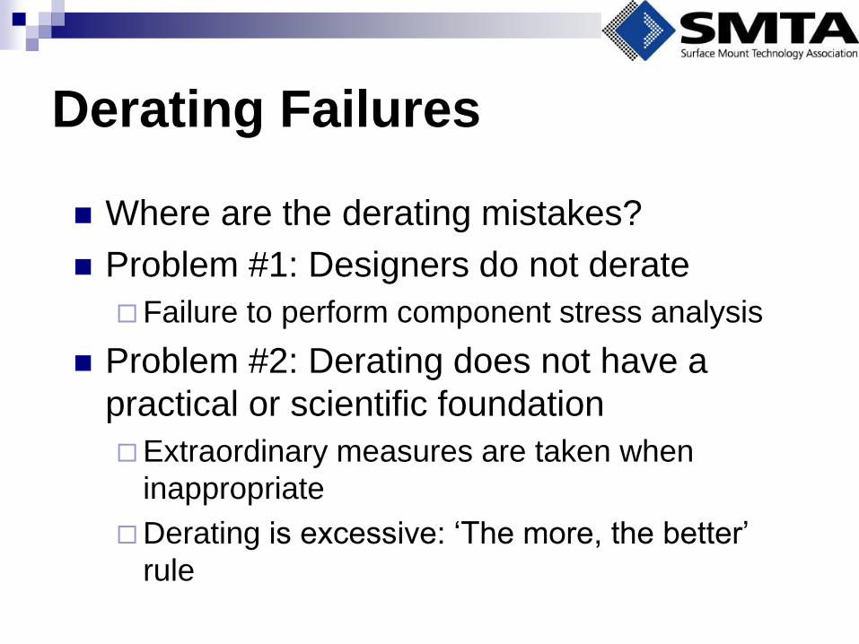
Where are the derating mistakes?
Problem #1: Designers do not derate
Failure to perform component stress analysis
Problem #2: Derating does not have a
practical or scientific foundation
Extraordinary measures are taken when
inappropriate
Derating is excessive: ‘The more, the better’
rule
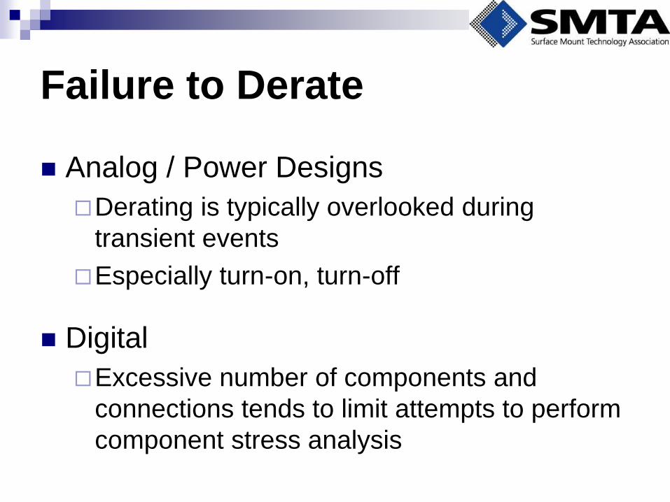
Failure to Derate
Analog / Power Designs
Derating is typically overlooked during
transient events
Especially turn-on, turn-off
Digital
Excessive number of components and
connections tends to limit attempts to perform
component stress analysis
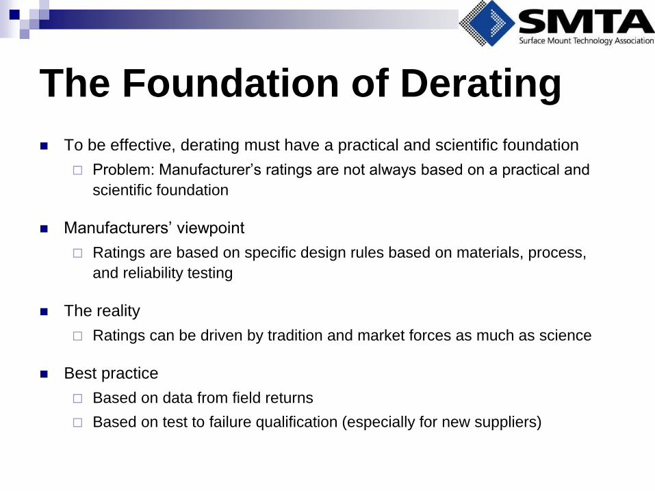
The Foundation of Derating
To be effective, derating must have a practical and scientific foundation
Problem: Manufacturer’s ratings are not always based on a practical and
scientific foundation
Manufacturers’ viewpoint
Ratings are based on specific design rules based on materials, process,
and reliability testing
The reality
Ratings can be driven by tradition and market forces as much as science
Best practice
Based on data from field returns
Based on test to failure qualification (especially for new suppliers)
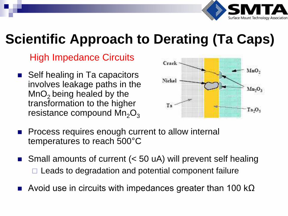
Scientific Approach to Derating (Ta Caps)
Self healing in Ta capacitors involves leakage paths in the MnO2 being healed by the transformation to the higher resistance compound Mn2O3
Process requires enough current to allow internal temperatures to reach 500°C
Small amounts of current (< 50 uA) will prevent self healing
Leads to degradation and potential component failure
Avoid use in circuits with impedances greater than 100 kΩ
High Impedance Circuits
Derating Decision Tree
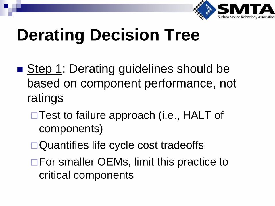
Step 1: Derating guidelines should be
based on component performance, not
ratings
Test to failure approach (i.e., HALT of
components)
Quantifies life cycle cost tradeoffs
For smaller OEMs, limit this practice to
critical components
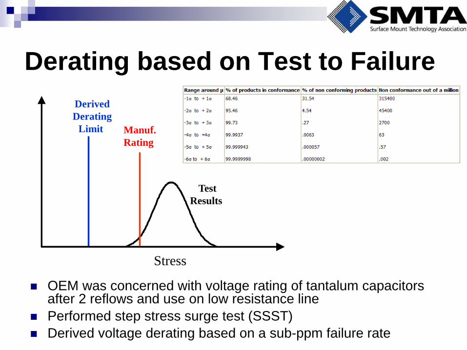
Derating based on Test to Failure
OEM was concerned with voltage rating of tantalum capacitors after 2 reflows and use on low resistance line
Performed step stress surge test (SSST)
Derived voltage derating based on a sub-ppm failure rate
Stress
Derived
Derating
Limit
Test
Results
Manuf.
Rating
Derating Decision Tree (continued)
Step 2: Derating guidelines should be based on
recommendations from the component manufacturer
They built it; they should know it
Don’t trust the manufacturer? Use someone else
Step 3: Derating guidelines should be based on
customer requirements
Step 4: Derating guidelines should be based
industry-accepted specification/standard
Be flexible, not absolute!
Robustness - Components
o Concerns
o Potential for latent defects after exposure to Pb-free reflow temperatures
o 215°C - 220°C peak → 240°C - 260°C peak
o Drivers
o Initial observations of deformed or damaged
components
o Failure of component manufacturers to update
specifications
o Components of particular interest
o Aluminum electrolytic capacitors
o Ceramic chip capacitors
o Surface mount connectors
o Specialty components (RF, optoelectronic, etc.)
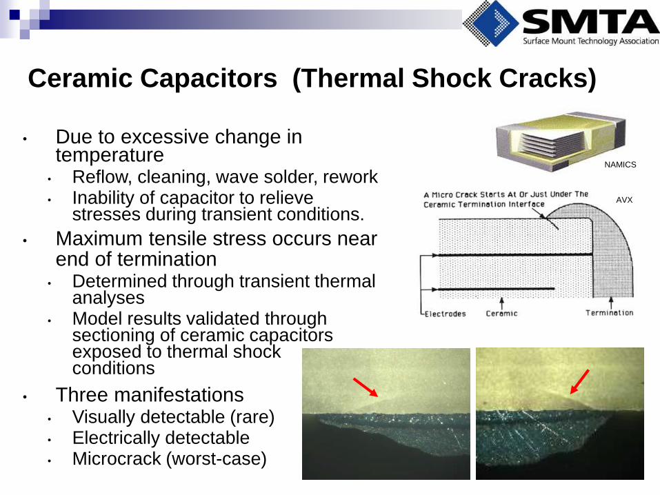
Ceramic Capacitors (Thermal Shock Cracks)
• Due to excessive change in temperature
• Reflow, cleaning, wave solder, rework • Inability of capacitor to relieve
stresses during transient conditions.
• Maximum tensile stress occurs near end of termination
• Determined through transient thermal analyses
• Model results validated through sectioning of ceramic capacitors exposed to thermal shock conditions
• Three manifestations • Visually detectable (rare) • Electrically detectable • Microcrack (worst-case)
NAMICS
AVX
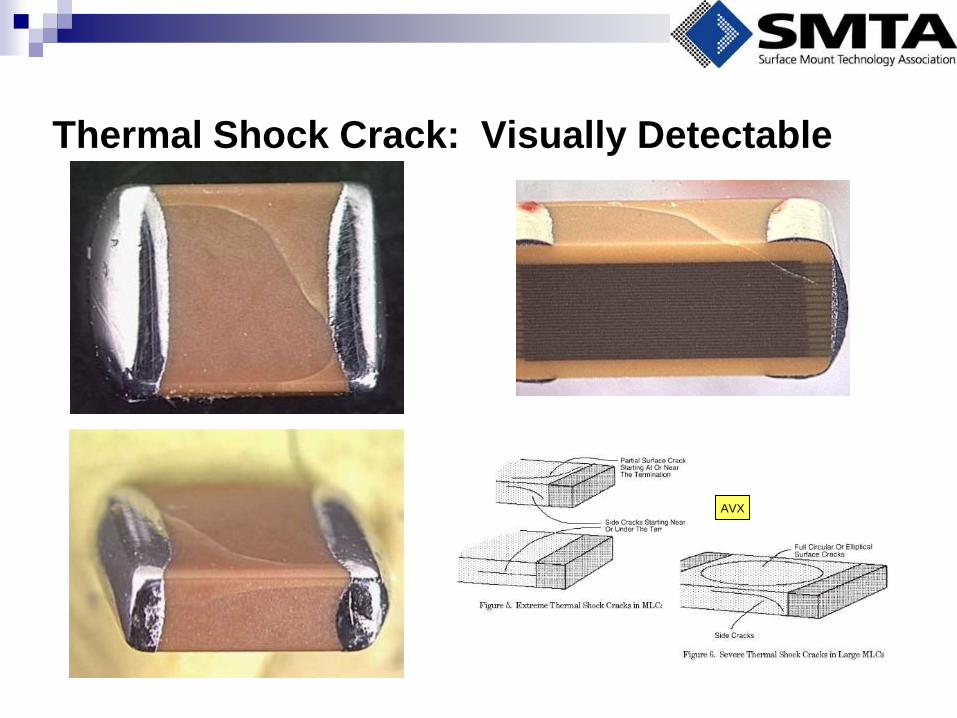
Thermal Shock Crack: Visually Detectable
AVX
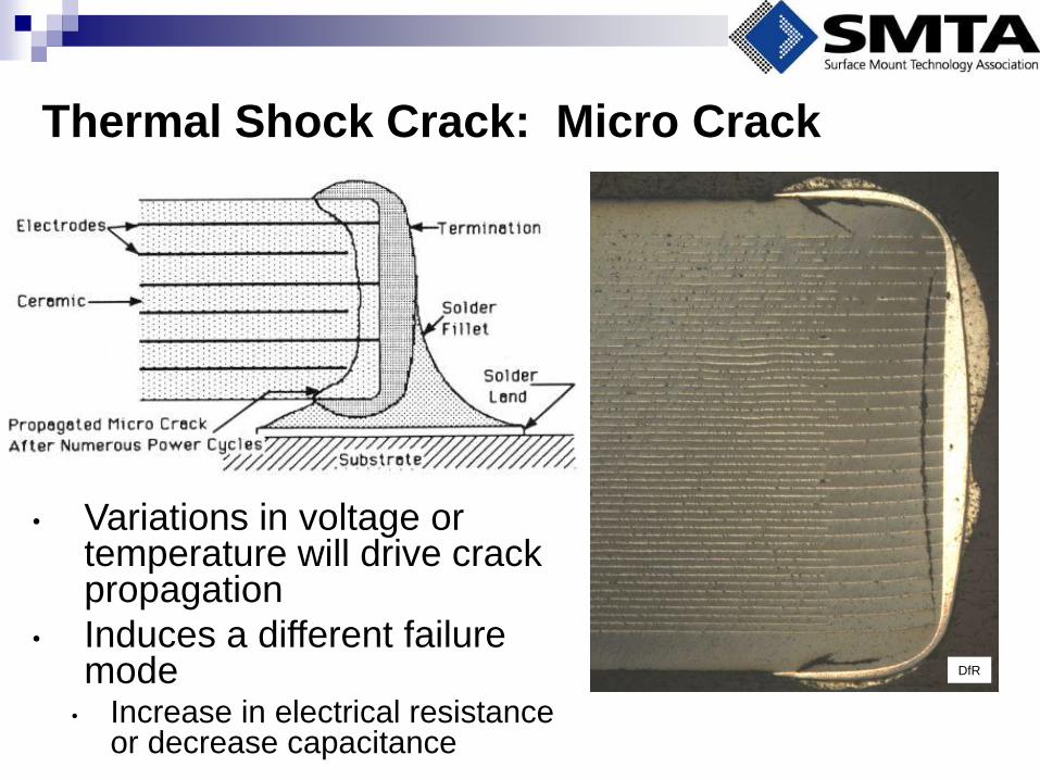
Thermal Shock Crack: Micro Crack
• Variations in voltage or temperature will drive crack propagation
• Induces a different failure mode
• Increase in electrical resistance or decrease capacitance
DfR
Module 3: Mechanisms and
Physics of Failure (PoF)
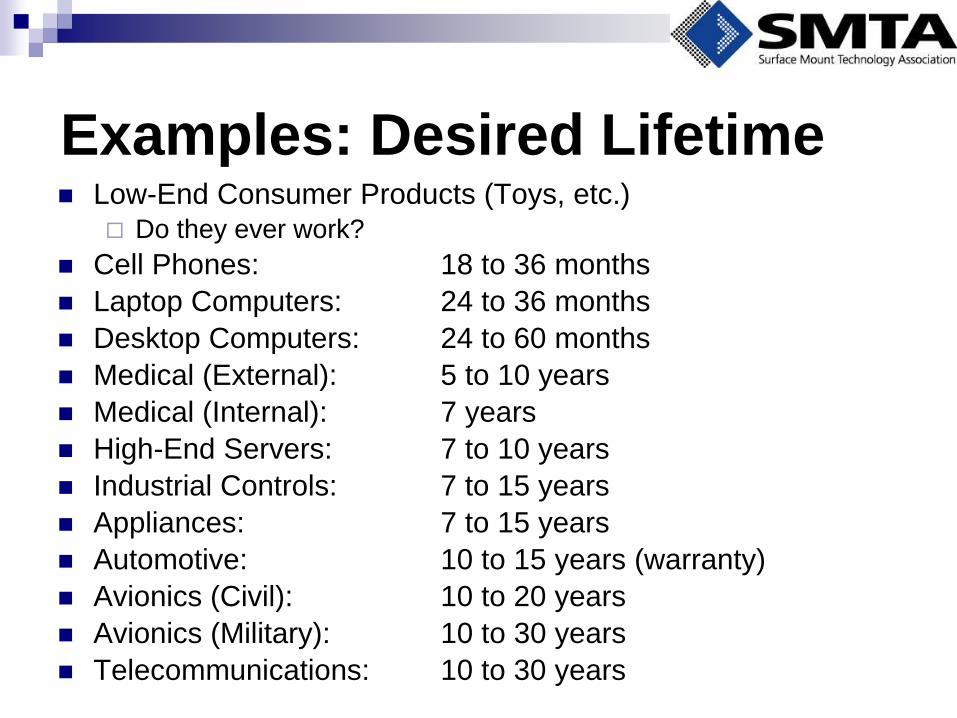
Examples: Desired Lifetime Low-End Consumer Products (Toys, etc.)
Do they ever work?
Cell Phones: 18 to 36 months
Laptop Computers: 24 to 36 months
Desktop Computers: 24 to 60 months
Medical (External): 5 to 10 years
Medical (Internal): 7 years
High-End Servers: 7 to 10 years
Industrial Controls: 7 to 15 years
Appliances: 7 to 15 years
Automotive: 10 to 15 years (warranty)
Avionics (Civil): 10 to 20 years
Avionics (Military): 10 to 30 years
Telecommunications: 10 to 30 years
Identify Field
Environment Approach 1: Use of industry/military
specifications
MIL-STD-810,
MIL-HDBK-310,
SAE J1211,
IPC-SM-785,
Telcordia GR3108,
IEC 60721-3, etc.
Advantages
No additional cost!
Sometimes very comprehensive
Agreement throughout the industry
Missing information? Consider standards from other industries
Disadvantages
Most more than 20 years old
Always less or greater than actual (by how much, unknown) IPC SM785
MIL HDBK310
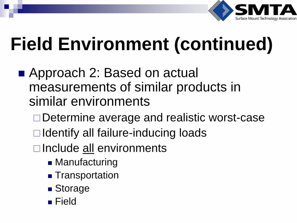
Field Environment (continued)
Approach 2: Based on actual measurements of similar products in similar environments
Determine average and realistic worst-case
Identify all failure-inducing loads
Include all environments Manufacturing
Transportation
Storage
Field
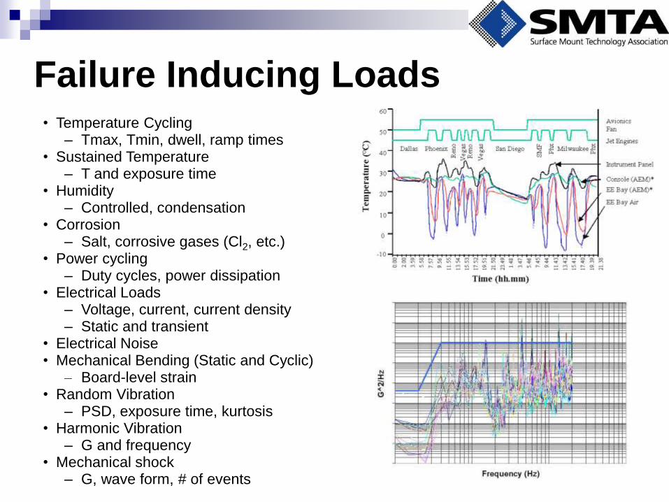
Failure Inducing Loads • Temperature Cycling
– Tmax, Tmin, dwell, ramp times • Sustained Temperature
– T and exposure time • Humidity
– Controlled, condensation • Corrosion
– Salt, corrosive gases (Cl2, etc.) • Power cycling
– Duty cycles, power dissipation • Electrical Loads
– Voltage, current, current density – Static and transient
• Electrical Noise • Mechanical Bending (Static and Cyclic)
– Board-level strain • Random Vibration
– PSD, exposure time, kurtosis • Harmonic Vibration
– G and frequency • Mechanical shock
– G, wave form, # of events
Field Environment (Best Practice)
Use standards when… Certain aspects of your environment are common
No access to use environment
Measure when… Certain aspects of your environment are unique
Strong relationship with customer
Do not mistake test specifications for the actual use environment Common mistake with vibration loads
PoF and Wearout What is susceptible to long-term degradation in electronic designs?
Ceramic Capacitors (dielectric breakdown)
Electrolytic Capacitors (electrolyte evaporation, dielectric dissolution)
Resistors (if improperly derated)
Silver-Based Platings (if exposed to corrosive environments)
Relays and other Electromechanical Components (wearout models
not well developed)
Connectors (if improperly specified and designed)
Tin Whiskers
Integrated Circuits (next generation feature size)
Interconnects (Creep, Fatigue)
Plated through holes
Solder joints
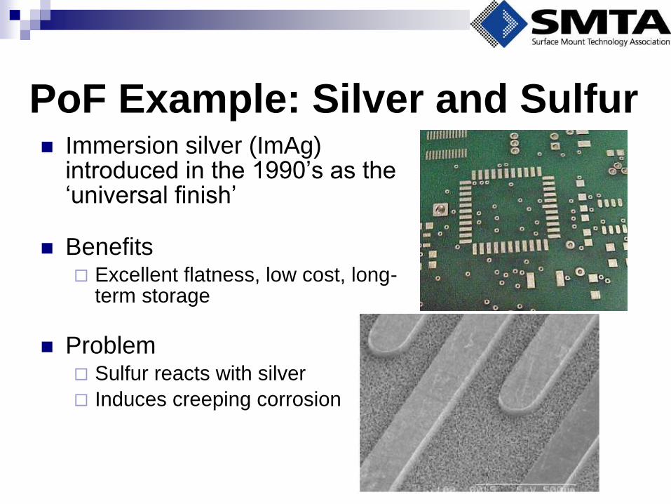
PoF Example: Silver and Sulfur Immersion silver (ImAg)
introduced in the 1990’s as the ‘universal finish’
Benefits Excellent flatness, low cost, long-
term storage
Problem Sulfur reacts with silver
Induces creeping corrosion
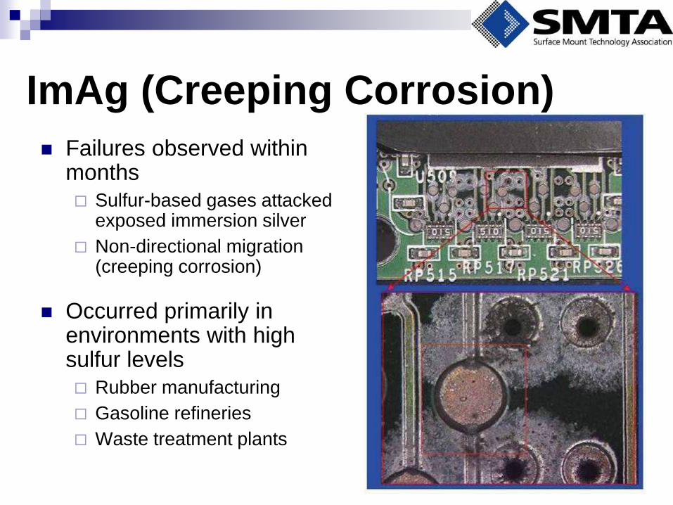
ImAg (Creeping Corrosion)
Failures observed within months
Sulfur-based gases attacked exposed immersion silver
Non-directional migration (creeping corrosion)
Occurred primarily in environments with high sulfur levels
Rubber manufacturing
Gasoline refineries
Waste treatment plants
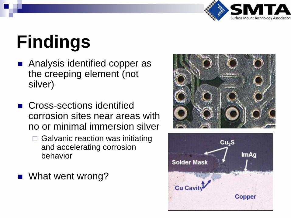
Findings Analysis identified copper as
the creeping element (not silver)
Cross-sections identified corrosion sites near areas with no or minimal immersion silver
Galvanic reaction was initiating and accelerating corrosion behavior
What went wrong?
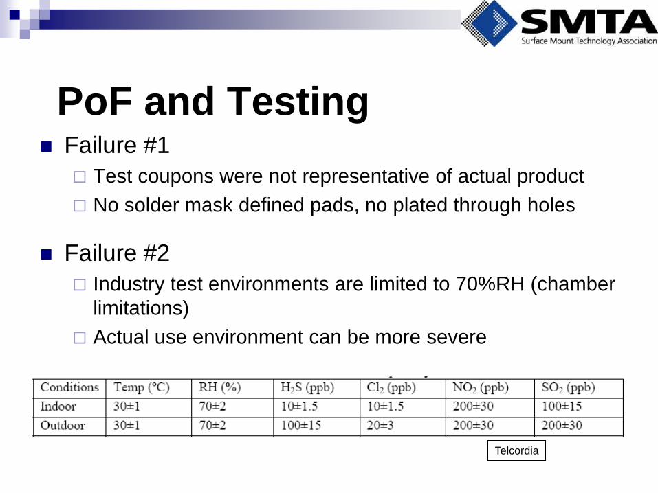
PoF and Testing Failure #1
Test coupons were not representative of actual product
No solder mask defined pads, no plated through holes
Failure #2
Industry test environments are limited to 70%RH (chamber
limitations)
Actual use environment can be more severe
Telcordia

PoF and Immersion Silver
The Final Failure?
Acknowledging the reactivity of silver with
sulfur and moving beyond ‘test to spec’ to
truly capture potential risks
The ‘physics’ was not well enough understood
before the new material was released
Alternatives to PoF
Step 1: Rules of Thumb
Step 2: Best Practice
Follow part selection guidelines
Step 3: Norris-Landzsberg
Rules of Thumb (Constant
Temperature)
Electrolytic Capacitor lifetime becomes an issue when ambient temperatures begin to exceed 40C on a constant basis
85C/2000 hour ratings tend to be insufficient for more than 5 year life
Many companies limit solder joint temperature to a maximum of 75ºC – 85ºC
Some limit IC junction temperature to a similar range
Rules of Thumb (Temperature Cycling)
In nominal environments, solder joint wearout is unlikely
Low power, diurnal cycling
∆25C, 1 cycle per day
Lifetime of less than 10 years
Greater concerns in more severe environments
Diurnal heat sources with sufficient fluctuation (∆40C)
Diurnal power dissipation of ∆40C and greater
Power cycling greater than 4 cycles/day (mini-cycling)
Rules of Thumb (Temp Cycling)(cont.)
If a solder joint fatigue is a concern, manage package styles MELF parts (SMA and SMB available)
Crystals on ceramic substrates (especially large ones)
Chip resistors greater than 1812 or capacitors greater than 2225
Large memory devices (44, 56, 66 I/O) with Alloy 42 leadframes
Large I/O (≥ 44) quad flat pack no-lead (QFN)
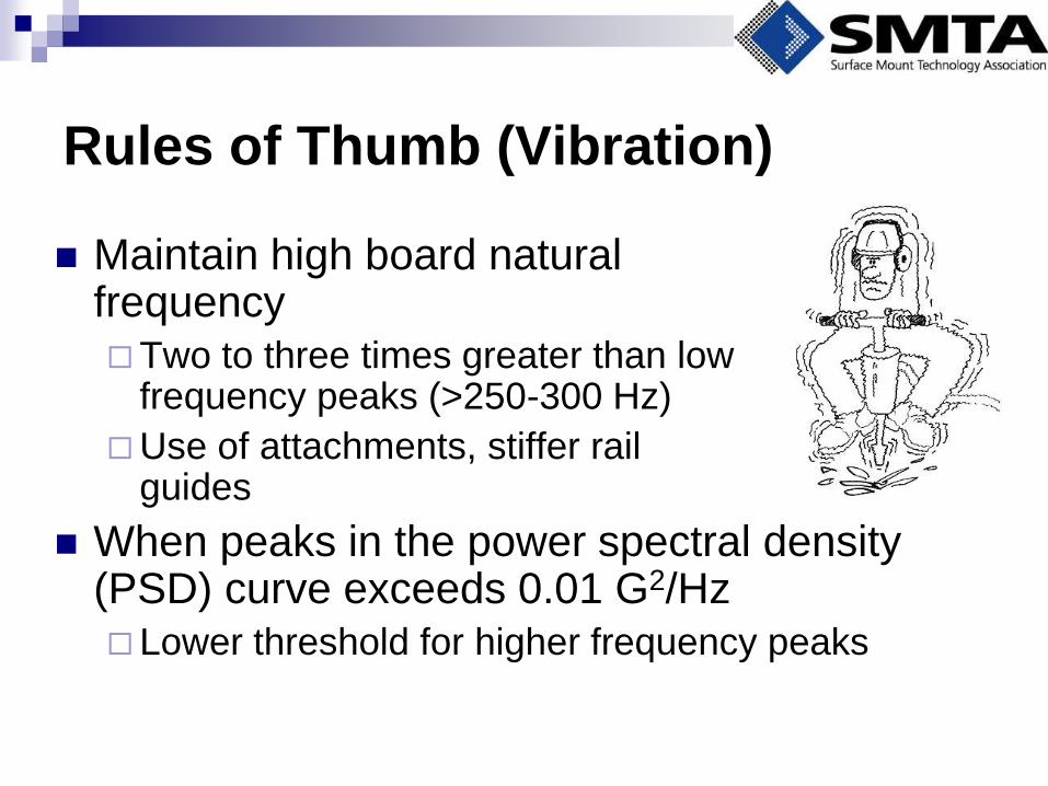
Rules of Thumb (Vibration)
Maintain high board natural frequency
Two to three times greater than low frequency peaks (>250-300 Hz)
Use of attachments, stiffer rail guides
When peaks in the power spectral density (PSD) curve exceeds 0.01 G2/Hz
Lower threshold for higher frequency peaks
Vibration (continued)
Failures primarily occur when peak loads occur at similar frequencies as the natural frequency of the product / design
Natural frequencies
Larger boards, simply supported: 60 – 150 Hz
Smaller boards, wedge locked: 200 – 500 Hz
Gold wire bonds: 2k – 4kHz
Aluminum wire bonds: >10kHz
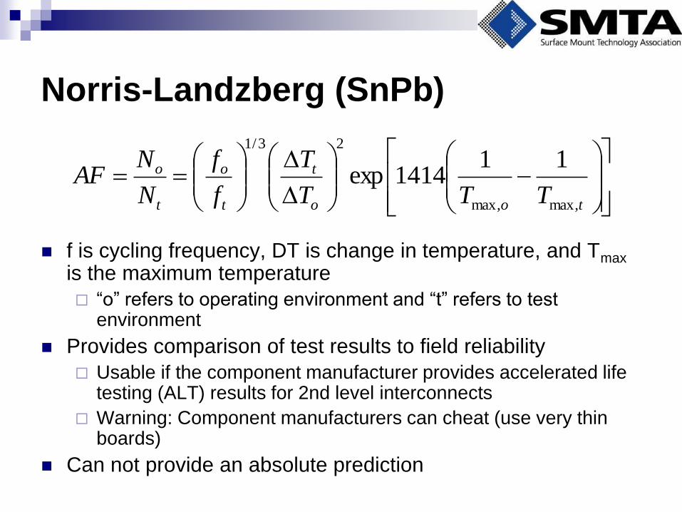
Norris-Landzberg (SnPb)
f is cycling frequency, DT is change in temperature, and Tmax is the maximum temperature
“o” refers to operating environment and “t” refers to test environment
Provides comparison of test results to field reliability
Usable if the component manufacturer provides accelerated life testing (ALT) results for 2nd level interconnects
Warning: Component manufacturers can cheat (use very thin boards)
Can not provide an absolute prediction
too
t
t
o
t
o
TTT
T
f
f
N
NAF
max,max,
23/1
111414exp
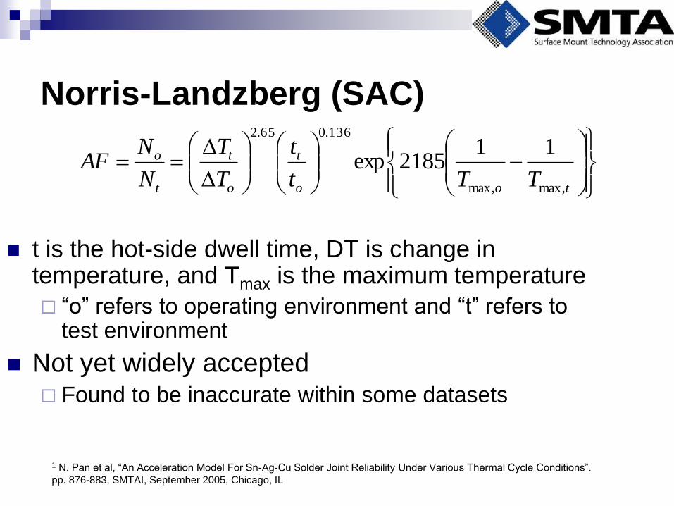
Norris-Landzberg (SAC)
too
t
o
t
t
o
TTt
t
T
T
N
NAF
max,max,
136.065.2
112185exp
t is the hot-side dwell time, DT is change in temperature, and Tmax is the maximum temperature
“o” refers to operating environment and “t” refers to test environment
Not yet widely accepted Found to be inaccurate within some datasets
1 N. Pan et al, “An Acceleration Model For Sn-Ag-Cu Solder Joint Reliability Under Various Thermal Cycle Conditions”.
pp. 876-883, SMTAI, September 2005, Chicago, IL
Long-Term Reliability
Rules of Thumb, Best Practices, and
Norris-Landzberg are not always sufficient
Good first pass
When the risk is too high, physics of failure
(PoF) calculations are irreplaceable
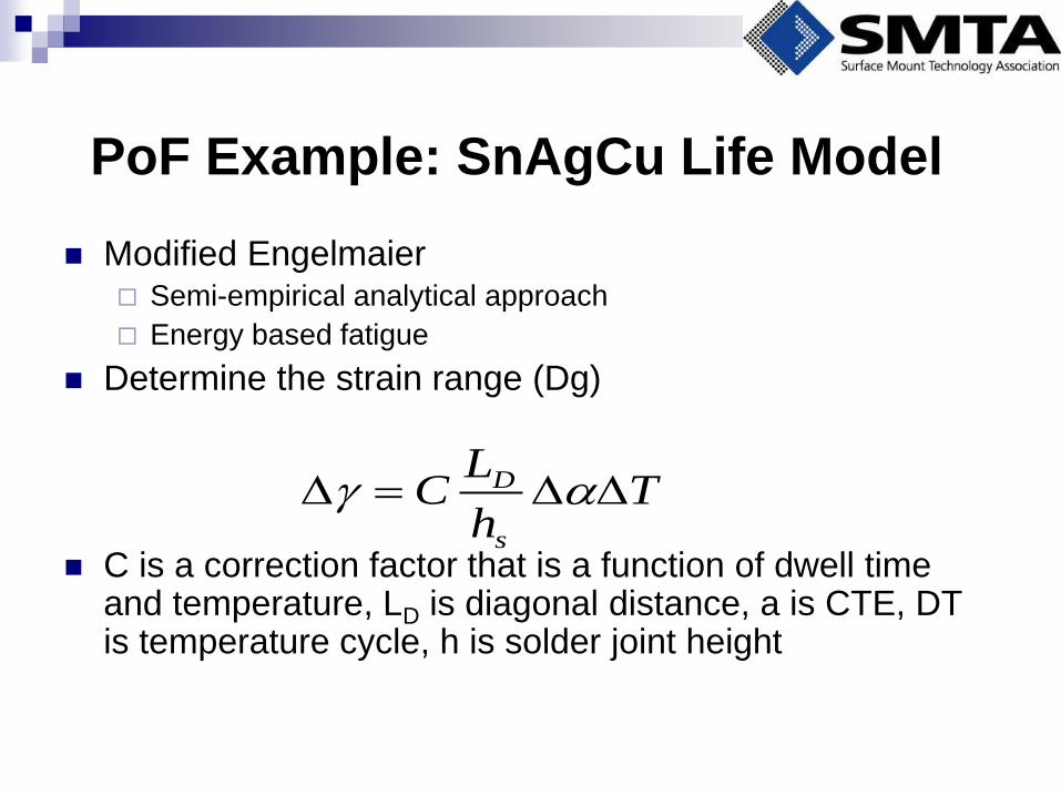
PoF Example: SnAgCu Life Model
Modified Engelmaier Semi-empirical analytical approach
Energy based fatigue
Determine the strain range (Dg)
C is a correction factor that is a function of dwell time and temperature, LD is diagonal distance, a is CTE, DT is temperature cycle, h is solder joint height
Th
LC
s
D
PoF Example – SAC Model (cont.)
aGGA
h
GA
h
AE
L
AE
LFLT
bcc
c
ss
s
9
2
221112
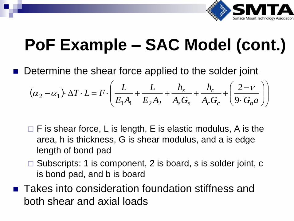
Determine the shear force applied to the solder joint
F is shear force, L is length, E is elastic modulus, A is the
area, h is thickness, G is shear modulus, and a is edge
length of bond pad
Subscripts: 1 is component, 2 is board, s is solder joint, c
is bond pad, and b is board
Takes into consideration foundation stiffness and
both shear and axial loads
PoF Example – SAC Model (cont.)
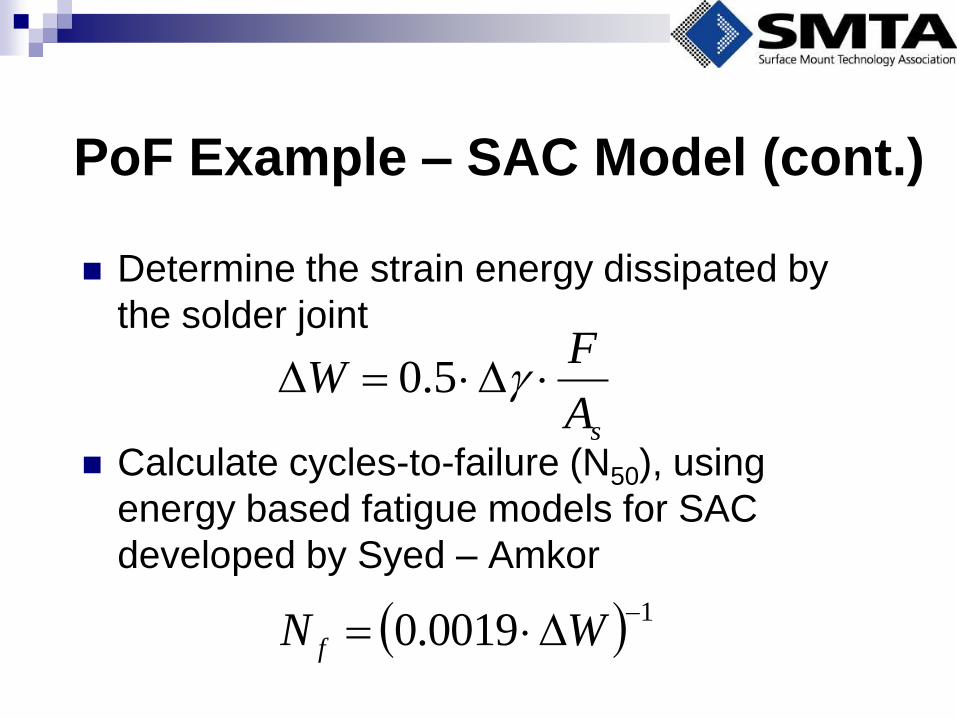
Determine the strain energy dissipated by
the solder joint
Calculate cycles-to-failure (N50), using
energy based fatigue models for SAC
developed by Syed – Amkor
10019.0
WN f
sA
FW 5.0
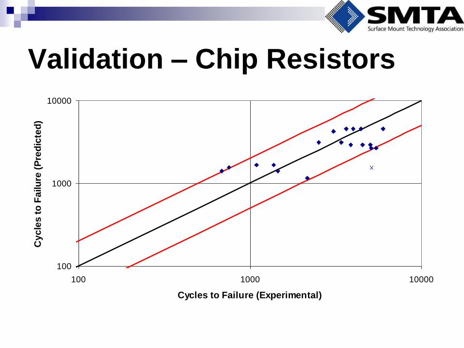
Validation – Chip Resistors
100
1000
10000
100 1000 10000
Cycles to Failure (Experimental)
Cy
cle
s t
o F
ailu
re (
Pre
dic
ted
)
PoF Example – SAC Reliability
(cont.)
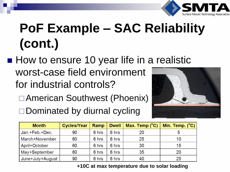
How to ensure 10 year life in a realistic
worst-case field environment
for industrial controls?
American Southwest (Phoenix)
Dominated by diurnal cycling
+10C at max temperature due to solar loading
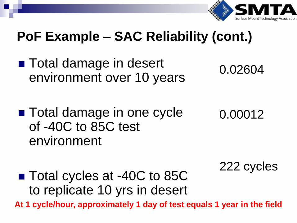
PoF Example – SAC Reliability (cont.)
Total damage in desert environment over 10 years
Total damage in one cycle of -40C to 85C test environment
Total cycles at -40C to 85C to replicate 10 yrs in desert
0.02604
0.00012
222 cycles
At 1 cycle/hour, approximately 1 day of test equals 1 year in the field
Module 4: Printed Circuit Boards
Surface Finishes
113
Importance of Surface Finish
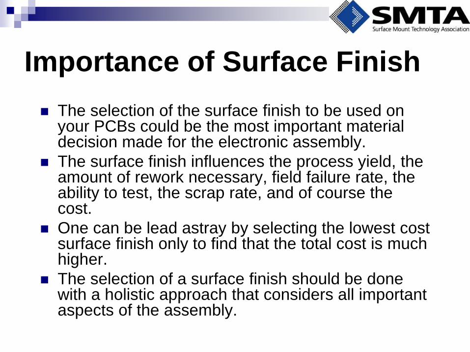
The selection of the surface finish to be used on your PCBs could be the most important material decision made for the electronic assembly.
The surface finish influences the process yield, the amount of rework necessary, field failure rate, the ability to test, the scrap rate, and of course the cost.
One can be lead astray by selecting the lowest cost surface finish only to find that the total cost is much higher.
The selection of a surface finish should be done with a holistic approach that considers all important aspects of the assembly.
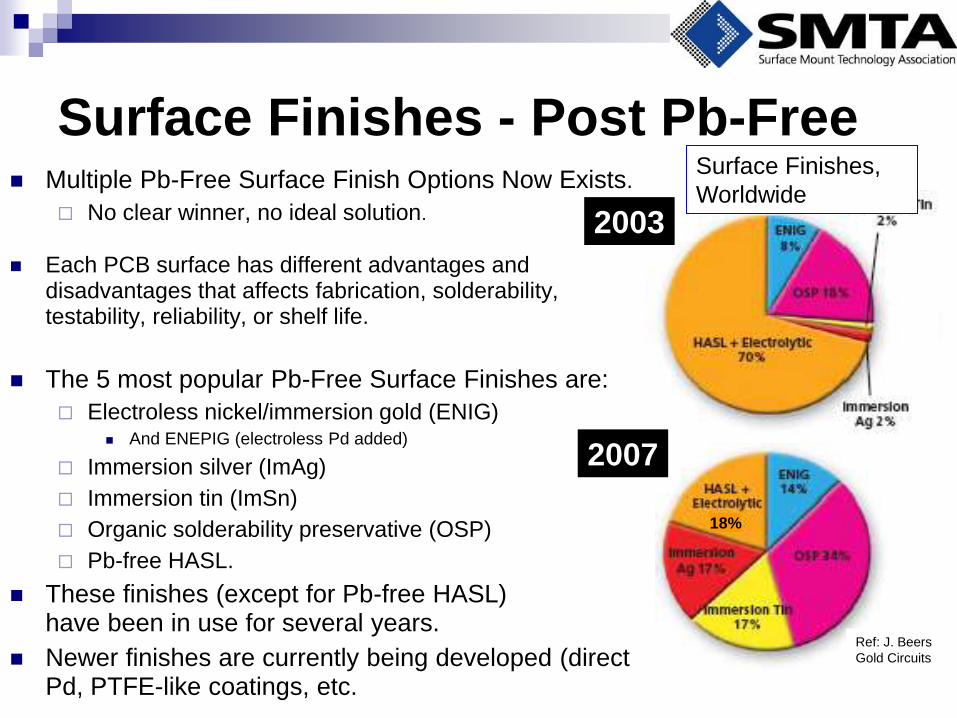
Surface Finishes - Post Pb-Free Multiple Pb-Free Surface Finish Options Now Exists.
No clear winner, no ideal solution.
Each PCB surface has different advantages and disadvantages that affects fabrication, solderability, testability, reliability, or shelf life.
The 5 most popular Pb-Free Surface Finishes are:
Electroless nickel/immersion gold (ENIG) And ENEPIG (electroless Pd added)
Immersion silver (ImAg)
Immersion tin (ImSn)
Organic solderability preservative (OSP)
Pb-free HASL.
These finishes (except for Pb-free HASL) have been in use for several years.
Newer finishes are currently being developed (direct Pd, PTFE-like coatings, etc.
18%
Surface Finishes,
Worldwide
2003
2007
Ref: J. Beers
Gold Circuits
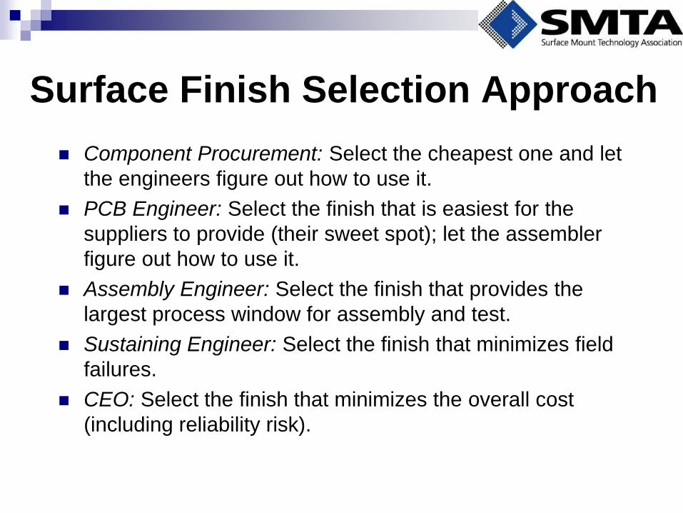
Surface Finish Selection Approach
Component Procurement: Select the cheapest one and let
the engineers figure out how to use it.
PCB Engineer: Select the finish that is easiest for the
suppliers to provide (their sweet spot); let the assembler
figure out how to use it.
Assembly Engineer: Select the finish that provides the
largest process window for assembly and test.
Sustaining Engineer: Select the finish that minimizes field
failures.
CEO: Select the finish that minimizes the overall cost
(including reliability risk).
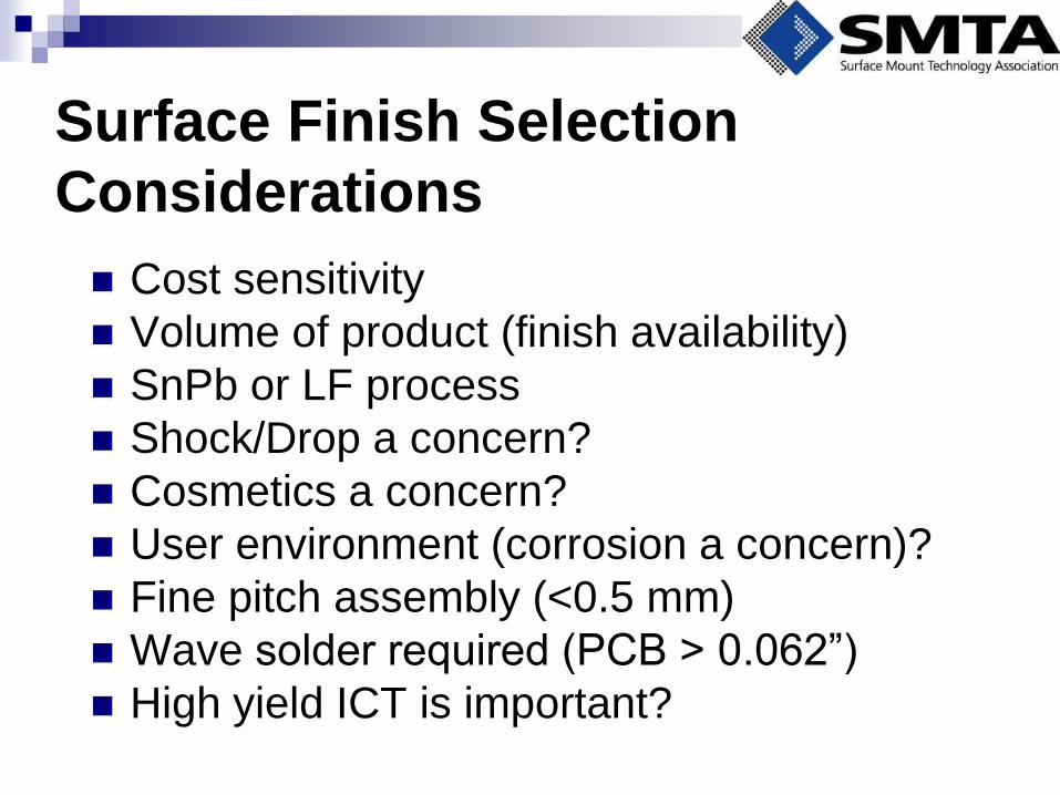
Surface Finish Selection
Considerations
Cost sensitivity
Volume of product (finish availability)
SnPb or LF process
Shock/Drop a concern?
Cosmetics a concern?
User environment (corrosion a concern)?
Fine pitch assembly (<0.5 mm)
Wave solder required (PCB > 0.062”)
High yield ICT is important?
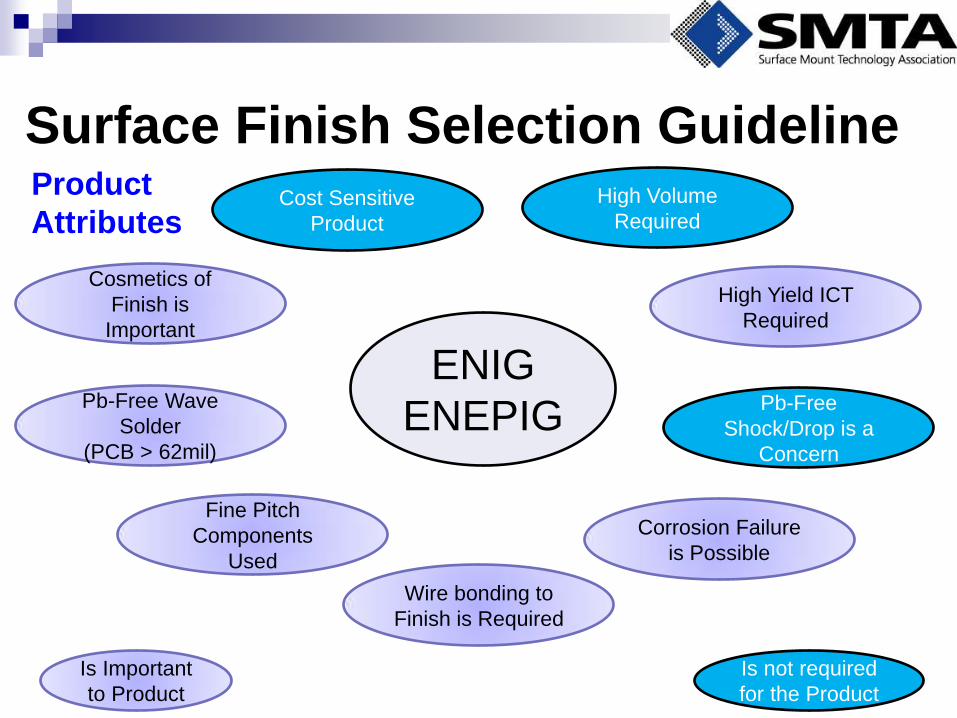
Surface Finish Selection Guideline
Cost Sensitive
Product
High Volume
Required
Pb-Free
Shock/Drop is a
Concern
Cosmetics of
Finish is
Important
Corrosion Failure
is Possible
Fine Pitch
Components
Used
Pb-Free Wave
Solder
(PCB > 62mil)
High Yield ICT
Required
Is Important
to Product
Is not required
for the Product
Attributes
Wire bonding to
Finish is Required
SF
Type
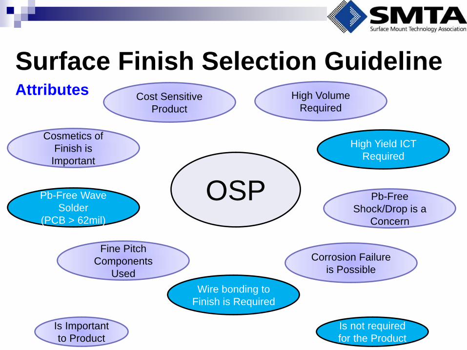
Surface Finish Selection Guideline Cost Sensitive
Product
High Volume
Required
Pb-Free
Shock/Drop is a
Concern
Cosmetics of
Finish is
Important
Corrosion Failure
is Possible
Fine Pitch
Components
Used
Pb-Free Wave
Solder
(PCB > 62mil)
High Yield ICT
Required
Is Important
to Product
Attributes
Wire bonding to
Finish is Required
OSP
Is not required
for the Product
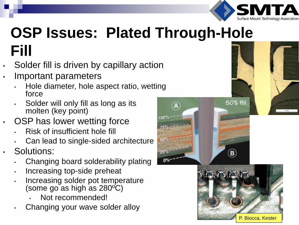
OSP Issues: Plated Through-Hole
Fill • Solder fill is driven by capillary action
• Important parameters • Hole diameter, hole aspect ratio, wetting
force
• Solder will only fill as long as its molten (key point)
• OSP has lower wetting force • Risk of insufficient hole fill
• Can lead to single-sided architecture
• Solutions: • Changing board solderability plating
• Increasing top-side preheat
• Increasing solder pot temperature (some go as high as 280ºC)
• Not recommended!
• Changing your wave solder alloy
P. Biocca, Kester
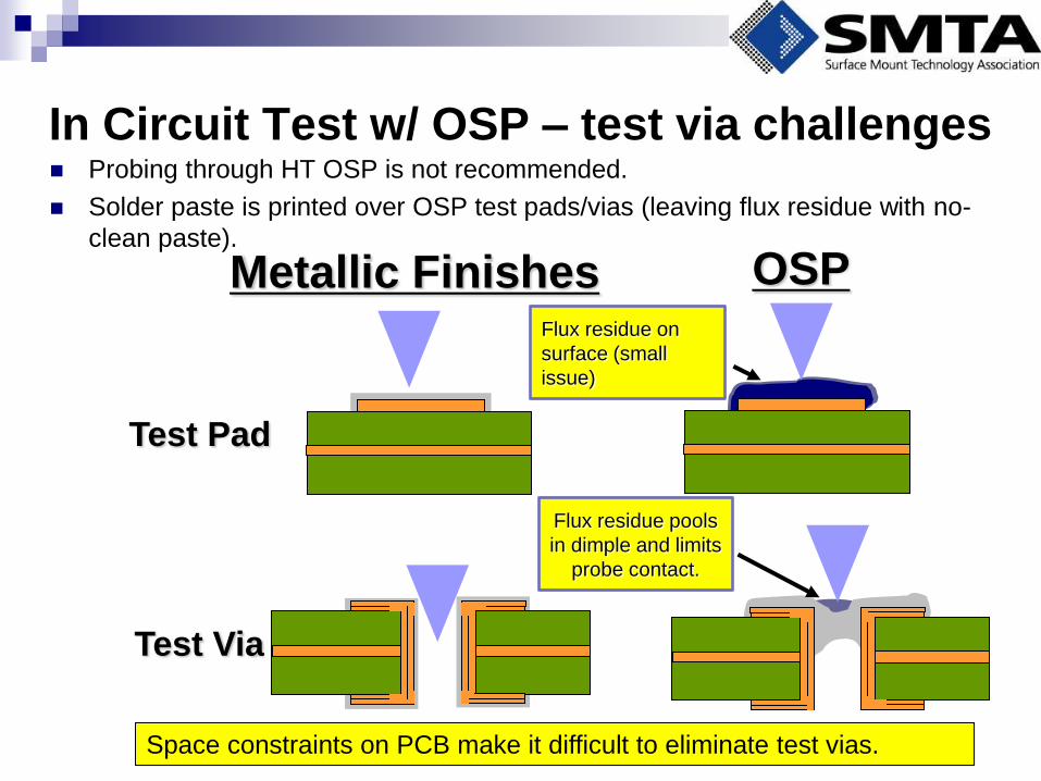
In Circuit Test w/ OSP – test via challenges Probing through HT OSP is not recommended.
Solder paste is printed over OSP test pads/vias (leaving flux residue with no-
clean paste).
OSP Metallic Finishes
Test Pad
Test Via
Space constraints on PCB make it difficult to eliminate test vias.
Flux residue pools
in dimple and limits
probe contact.
Flux residue on
surface (small
issue)
Surface Finish Selection Guideline Cost Sensitive
Product
High Volume
Required
Pb-Free
Shock/Drop is a
Concern
Cosmetics of
Finish is
Important
Corrosion Failure
is Possible
Fine Pitch
Components
Used
Pb-Free Wave
Solder
(PCB > 62mil)
High Yield ICT
Required
Is Important
to Product
Product
Attributes
Wire bonding to
Finish is Required
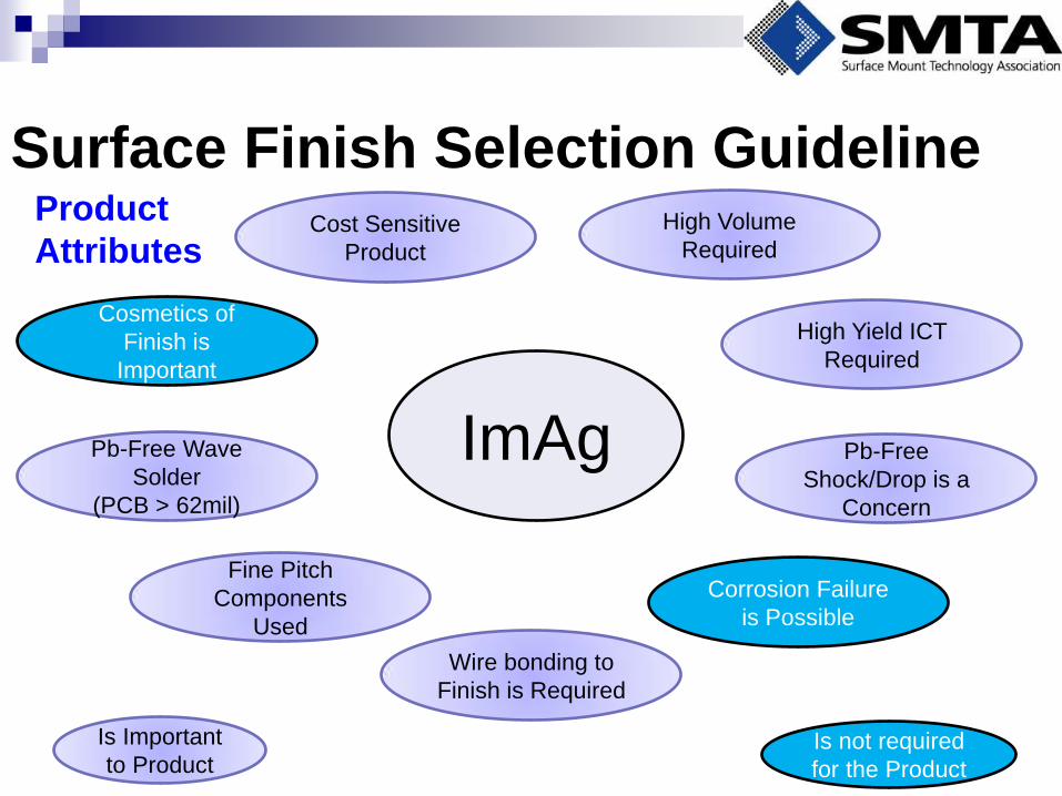
ImAg
Is not required
for the Product
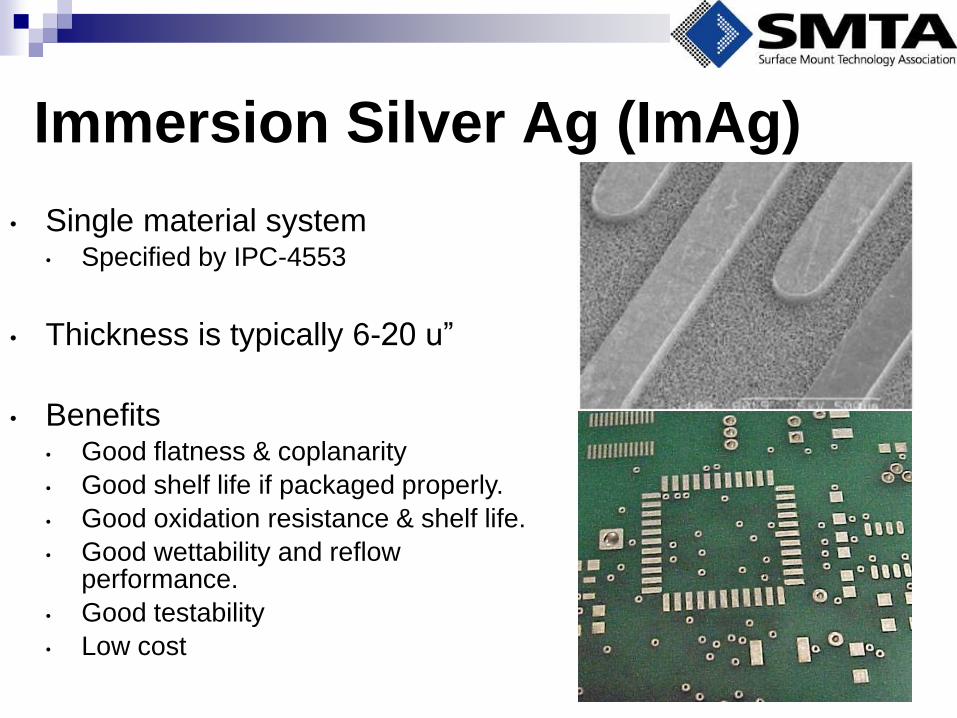
Immersion Silver Ag (ImAg)
• Single material system • Specified by IPC-4553
• Thickness is typically 6-20 u”
• Benefits • Good flatness & coplanarity
• Good shelf life if packaged properly.
• Good oxidation resistance & shelf life.
• Good wettability and reflow performance.
• Good testability
• Low cost
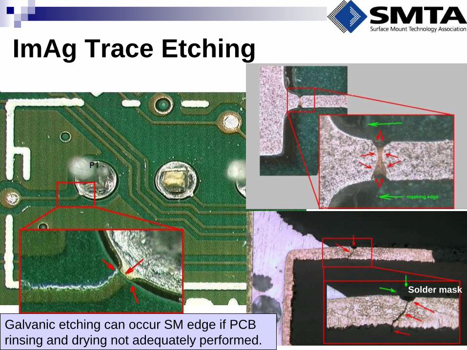
ImAg Trace Etching
Solder mask
Galvanic etching can occur SM edge if PCB
rinsing and drying not adequately performed.
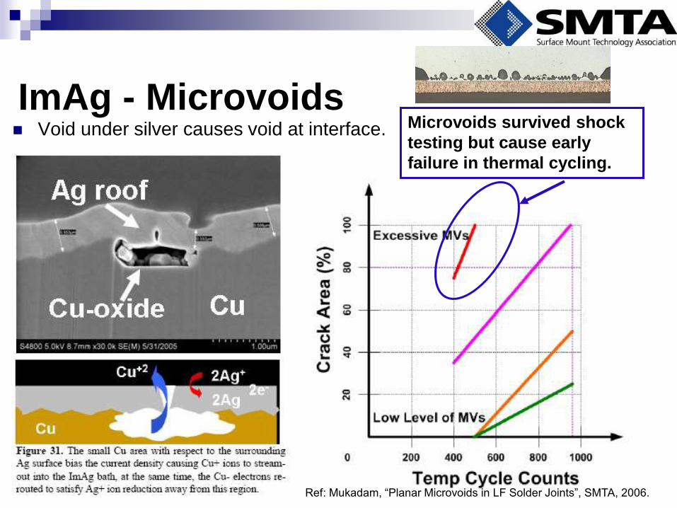
ImAg - Microvoids Void under silver causes void at interface.
Ref: Mukadam, “Planar Microvoids in LF Solder Joints”, SMTA, 2006.
Microvoids survived shock
testing but cause early
failure in thermal cycling.
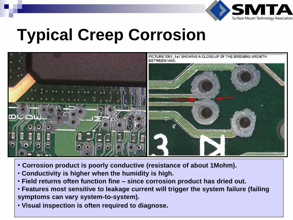
Typical Creep Corrosion
• Corrosion product is poorly conductive (resistance of about 1Mohm).
• Conductivity is higher when the humidity is high.
• Field returns often function fine – since corrosion product has dried out.
• Features most sensitive to leakage current will trigger the system failure (failing
symptoms can vary system-to-system).
• Visual inspection is often required to diagnose.
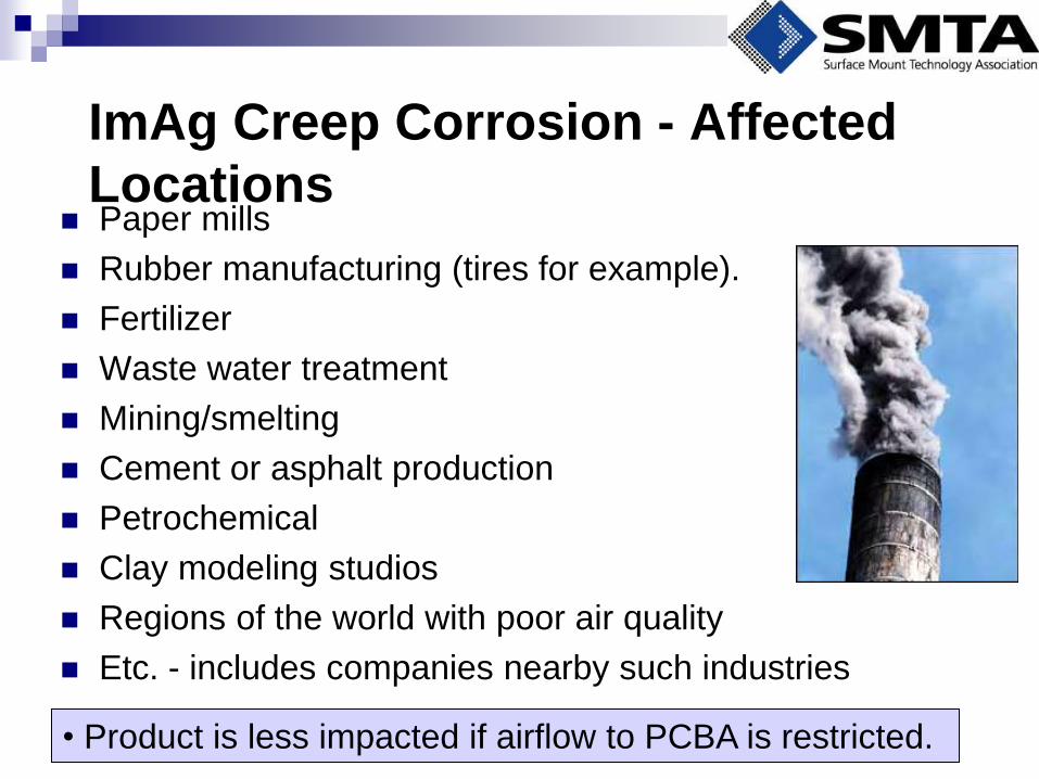
ImAg Creep Corrosion - Affected
Locations Paper mills
Rubber manufacturing (tires for example).
Fertilizer
Waste water treatment
Mining/smelting
Cement or asphalt production
Petrochemical
Clay modeling studios
Regions of the world with poor air quality
Etc. - includes companies nearby such industries
• Product is less impacted if airflow to PCBA is restricted.
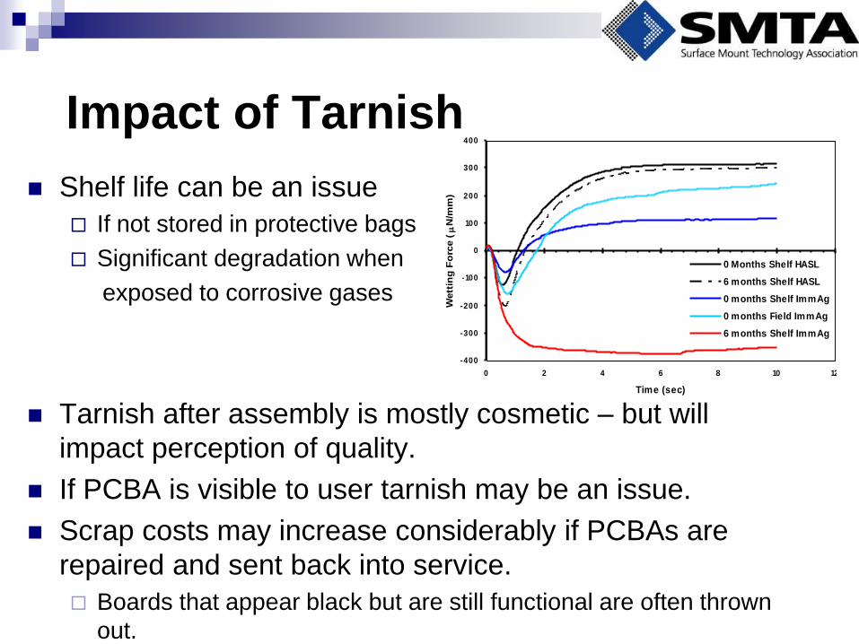
Impact of Tarnish
Shelf life can be an issue
If not stored in protective bags
Significant degradation when
exposed to corrosive gases
Tarnish after assembly is mostly cosmetic – but will
impact perception of quality.
If PCBA is visible to user tarnish may be an issue.
Scrap costs may increase considerably if PCBAs are
repaired and sent back into service.
Boards that appear black but are still functional are often thrown
out.
-400
-300
-200
-100
0
100
200
300
400
0 2 4 6 8 10 12
Time (sec)
Wett
ing
Fo
rce (m
N/m
m)
0 Months Shelf HASL
6 months Shelf HASL
0 months Shelf ImmAg
0 months Field ImmAg
6 months Shelf ImmAg
Surface Finish Selection Guideline Cost Sensitive
Product
High Volume
Required
Pb-Free
Shock/Drop is a
Concern
Cosmetics of
Finish is
Important
Corrosion Failure
is Possible
Fine Pitch
Components
Used
Pb-Free Wave
Solder
(PCB > 62mil)
High Yield ICT
Required
Is Important
to Product
Product
Attributes
Wire bonding to
Finish is Required
Is not required
for the Product
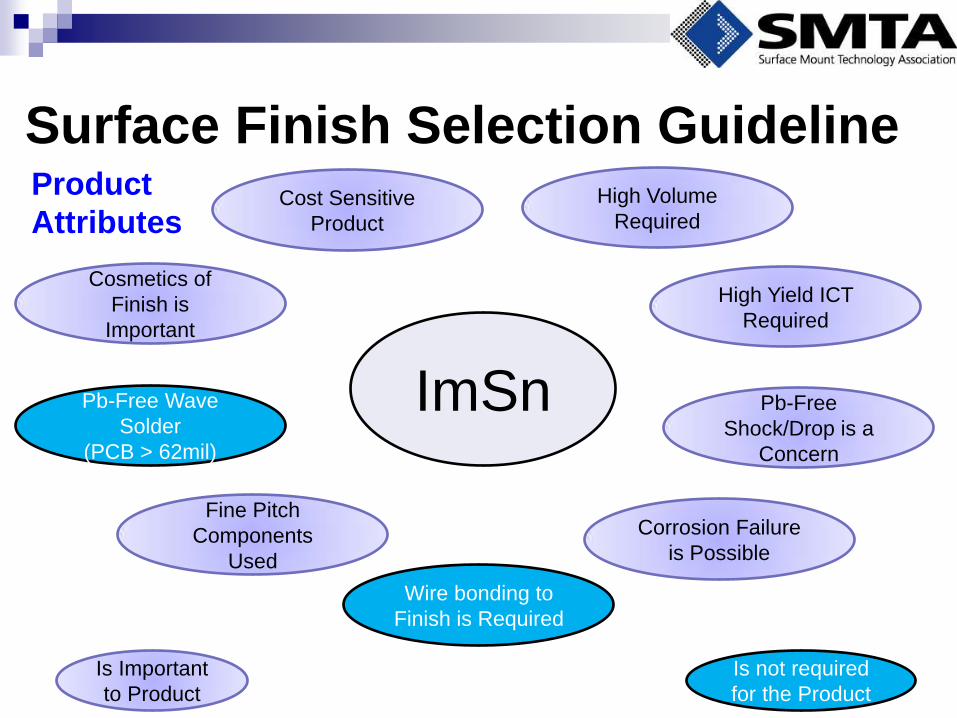
ImSn
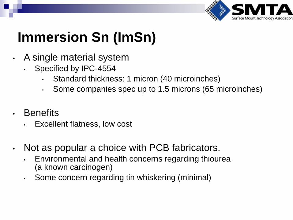
Immersion Sn (ImSn)
• A single material system • Specified by IPC-4554
• Standard thickness: 1 micron (40 microinches)
• Some companies spec up to 1.5 microns (65 microinches)
• Benefits • Excellent flatness, low cost
• Not as popular a choice with PCB fabricators. • Environmental and health concerns regarding thiourea
(a known carcinogen)
• Some concern regarding tin whiskering (minimal)
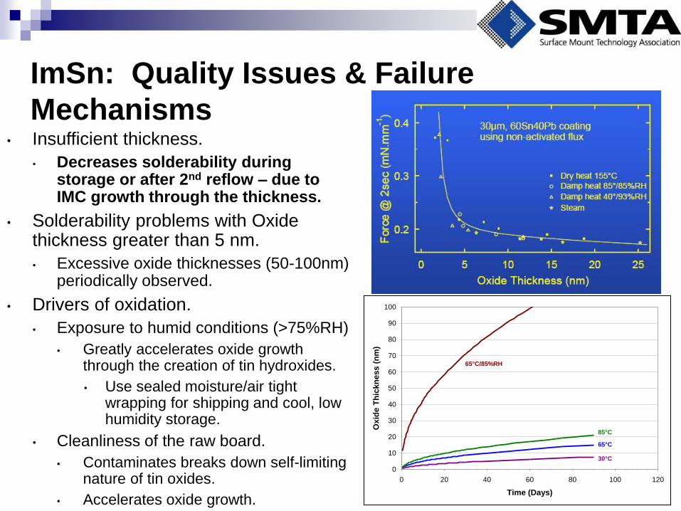
ImSn: Quality Issues & Failure
Mechanisms
0
10
20
30
40
50
60
70
80
90
100
0 20 40 60 80 100 120
Time (Days)
Ox
ide
Th
ickn
ess
(n
m)
30°C
65°C
85°C
65°C/85%RH
• Insufficient thickness.
• Decreases solderability during storage or after 2nd reflow – due to IMC growth through the thickness.
• Solderability problems with Oxide thickness greater than 5 nm.
• Excessive oxide thicknesses (50-100nm) periodically observed.
• Drivers of oxidation.
• Exposure to humid conditions (>75%RH)
• Greatly accelerates oxide growth through the creation of tin hydroxides.
• Use sealed moisture/air tight wrapping for shipping and cool, low humidity storage.
• Cleanliness of the raw board.
• Contaminates breaks down self-limiting nature of tin oxides.
• Accelerates oxide growth.
Surface Finish Selection Guideline Cost Sensitive
Product
High Volume
Required
Pb-Free
Shock/Drop is a
Concern
Cosmetics of
Finish is
Important
Corrosion Failure
is Possible
Fine Pitch
Components
Used
Pb-Free Wave
Solder
(PCB > 62mil)
High Yield ICT
Required
Is Important
to Product
Product
Attributes
Wire bonding to
Finish is Required
Is not required
for the Product
ENIG
ENEPIG
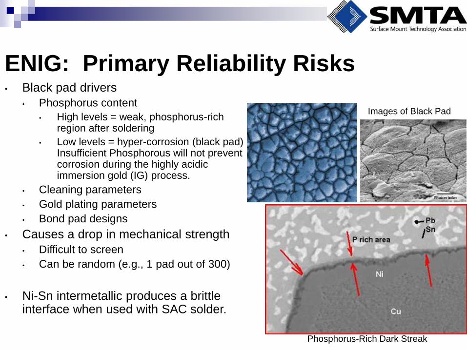
ENIG: Primary Reliability Risks
• Black pad drivers
• Phosphorus content
• High levels = weak, phosphorus-rich region after soldering
• Low levels = hyper-corrosion (black pad) Insufficient Phosphorous will not prevent corrosion during the highly acidic immersion gold (IG) process.
• Cleaning parameters
• Gold plating parameters
• Bond pad designs
• Causes a drop in mechanical strength
• Difficult to screen
• Can be random (e.g., 1 pad out of 300)
• Ni-Sn intermetallic produces a brittle interface when used with SAC solder.
Images of Black Pad
Phosphorus-Rich Dark Streak
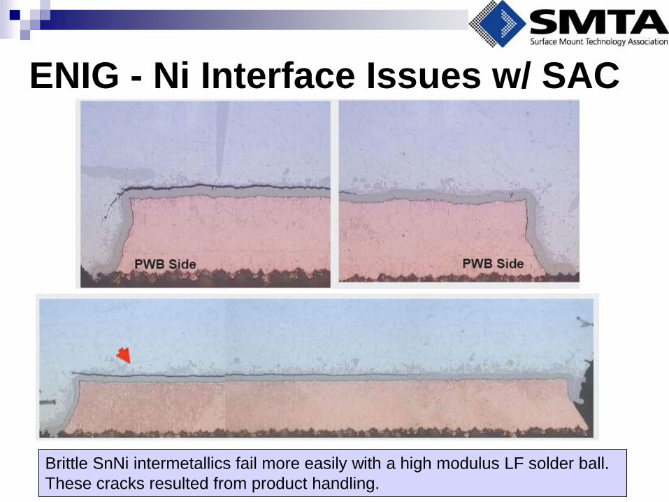
ENIG - Ni Interface Issues w/ SAC
Brittle SnNi intermetallics fail more easily with a high modulus LF solder ball.
These cracks resulted from product handling.
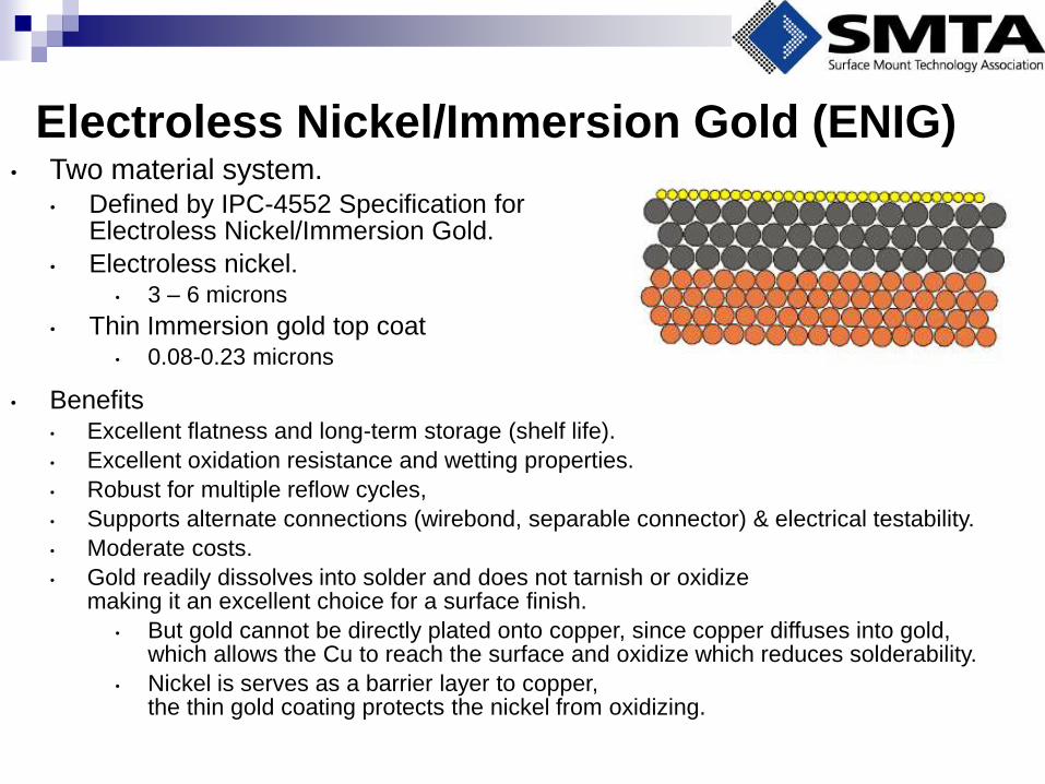
Electroless Nickel/Immersion Gold (ENIG) • Two material system.
• Defined by IPC-4552 Specification for Electroless Nickel/Immersion Gold.
• Electroless nickel. • 3 – 6 microns
• Thin Immersion gold top coat • 0.08-0.23 microns
• Benefits • Excellent flatness and long-term storage (shelf life).
• Excellent oxidation resistance and wetting properties.
• Robust for multiple reflow cycles,
• Supports alternate connections (wirebond, separable connector) & electrical testability.
• Moderate costs.
• Gold readily dissolves into solder and does not tarnish or oxidize making it an excellent choice for a surface finish.
• But gold cannot be directly plated onto copper, since copper diffuses into gold, which allows the Cu to reach the surface and oxidize which reduces solderability.
• Nickel is serves as a barrier layer to copper, the thin gold coating protects the nickel from oxidizing.
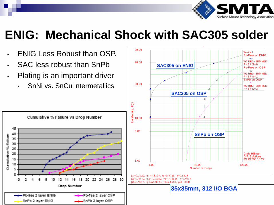
ENIG: Mechanical Shock with SAC305 solder
• ENIG Less Robust than OSP.
• SAC less robust than SnPb
• Plating is an important driver
• SnNi vs. SnCu intermetallics
1.00 100.0010.00
1.00
5.00
10.00
50.00
90.00
99.00
R eliaSoft's W eibull++ 6.0 - w w w .W eibull.c om
Probability - Weibull
Number of Drops
Unre
liability
, F(t
)
7/29/2005 10:27DfR SolutionsCraig Hillman
WeibullPb-Free on ENIG
W3 RR3 - SRM MEDF=6 / S=0
Pb-Free on OSP
W3 RR3 - SRM MEDF=5 / S=1
SnPb on OSP
W3 RR3 - SRM MEDF=3 / S=3
35x35mm, 312 I/O BGA
SAC305 on ENIG
SAC305 on OSP
SnPb on OSP
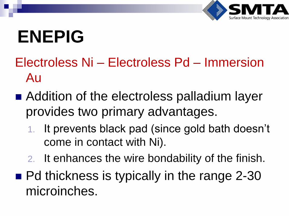
ENEPIG
Electroless Ni – Electroless Pd – Immersion
Au
Addition of the electroless palladium layer
provides two primary advantages.
1. It prevents black pad (since gold bath doesn’t
come in contact with Ni).
2. It enhances the wire bondability of the finish.
Pd thickness is typically in the range 2-30
microinches.
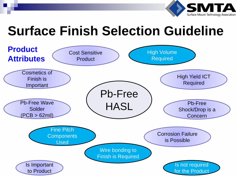
Surface Finish Selection Guideline
Cost Sensitive
Product
High Volume
Required
Pb-Free
Shock/Drop is a
Concern
Cosmetics of
Finish is
Important
Corrosion Failure
is Possible
Fine Pitch
Components
Used
Pb-Free Wave
Solder
(PCB > 62mil)
High Yield ICT
Required
Is Important
to Product
Product
Attributes
Wire bonding to
Finish is Required
Is not required
for the Product
Pb-Free
HASL

Pb-Free HASL (Hot Air Solder
Leveling) • Good choice when excellent solderability is required
• Thick boards that require LF wave soldering.
• Robust in multiple reflow cycles.
• Long shelf life required
• Flatness not as good as other finishes (but an improvement
over SnPb HASL).
• Could potentially be a problem with very fine pitch components
• High volume equipment is not yet in production.
• Horizontal LF lines are available but few are in production since high
volume demand is needed to make them cost effective.
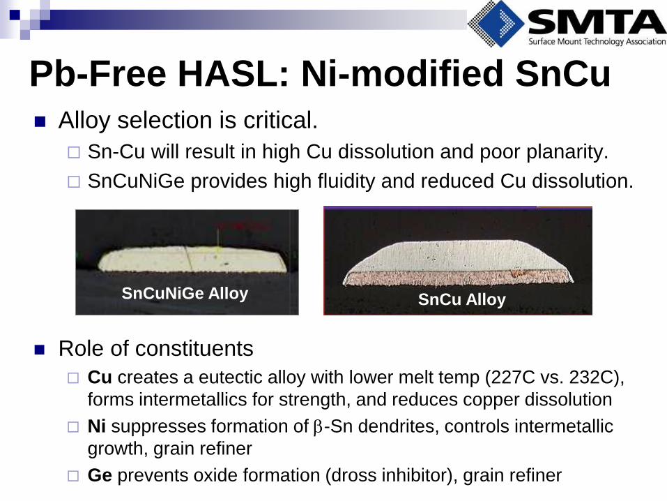
Pb-Free HASL: Ni-modified SnCu Alloy selection is critical.
Sn-Cu will result in high Cu dissolution and poor planarity.
SnCuNiGe provides high fluidity and reduced Cu dissolution.
Role of constituents
Cu creates a eutectic alloy with lower melt temp (227C vs. 232C),
forms intermetallics for strength, and reduces copper dissolution
Ni suppresses formation of -Sn dendrites, controls intermetallic
growth, grain refiner
Ge prevents oxide formation (dross inhibitor), grain refiner
SnCuNiGe Alloy SnCu Alloy
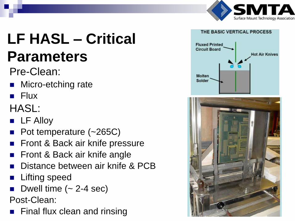
LF HASL – Critical
Parameters Pre-Clean: Micro-etching rate
Flux
HASL: LF Alloy
Pot temperature (~265C)
Front & Back air knife pressure
Front & Back air knife angle
Distance between air knife & PCB
Lifting speed
Dwell time (~ 2-4 sec)
Post-Clean:
Final flux clean and rinsing

Newer Finishes to the Market
Cost Sensitive
Product
High Volume
Required
Pb-Free
Shock/Drop is a
Concern
Cosmetics of
Finish is
Important
Corrosion Failure
is Possible
Fine Pitch
Components
Used
Pb-Free Wave
Solder
(PCB > 62mil)
High Yield ICT
Required
Is Important
to Product
Product
Attributes
Wire bonding to
Finish is Required
Is not required
for the Product
EPd
Needs verification
Lower cost than ENIG
Electroless Pd Process Sequence
Rin
se
Dry Micro
etch Activator E-Palladium
Rin
se
Rin
se
Rin
se
Rin
se
Acid
Cleaner
Pre
-Dip
Courtesy of OMGI
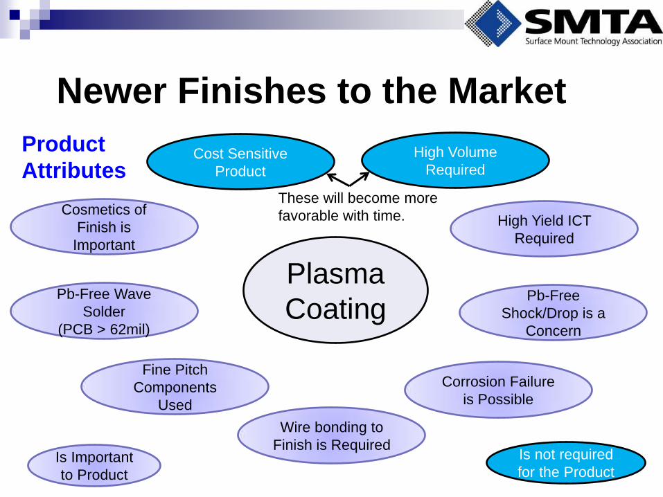
Newer Finishes to the Market
Cost Sensitive
Product
High Volume
Required
Pb-Free
Shock/Drop is a
Concern
Cosmetics of
Finish is
Important
Corrosion Failure
is Possible
Fine Pitch
Components
Used
Pb-Free Wave
Solder
(PCB > 62mil)
High Yield ICT
Required
Is Important
to Product
Product
Attributes
Wire bonding to
Finish is Required Is not required
for the Product
Plasma
Coating
These will become more
favorable with time.
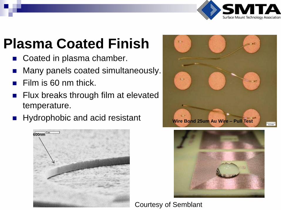
Plasma Coated Finish Coated in plasma chamber.
Many panels coated simultaneously.
Film is 60 nm thick.
Flux breaks through film at elevated
temperature.
Hydrophobic and acid resistant
600nm
Wire Bond 25um Au Wire – Pull Test
Courtesy of Semblant
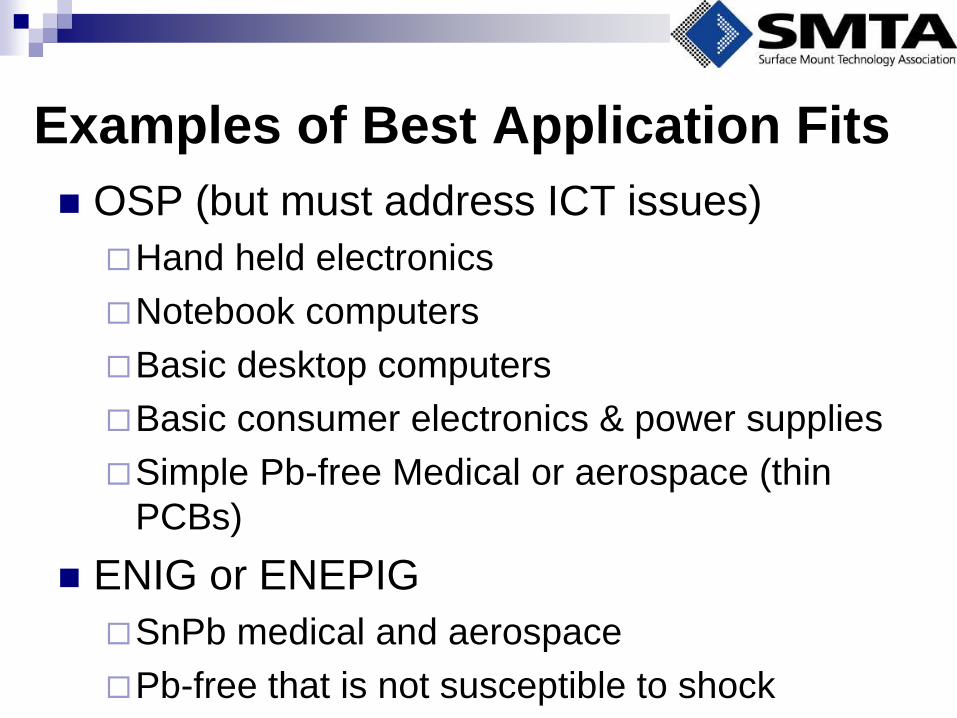
Examples of Best Application Fits
OSP (but must address ICT issues)
Hand held electronics
Notebook computers
Basic desktop computers
Basic consumer electronics & power supplies
Simple Pb-free Medical or aerospace (thin
PCBs)
ENIG or ENEPIG
SnPb medical and aerospace
Pb-free that is not susceptible to shock
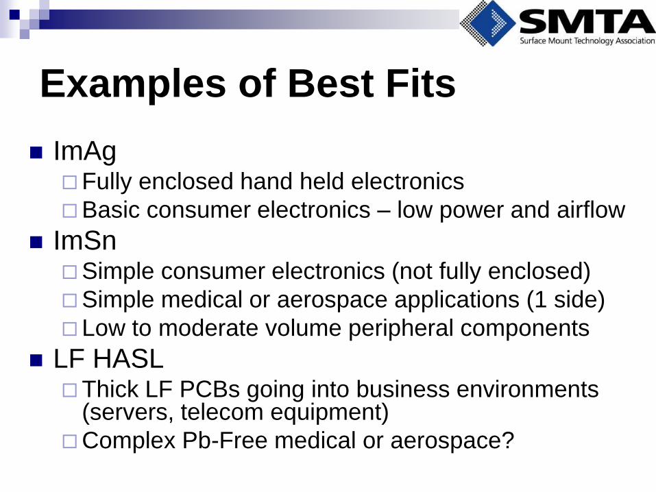
Examples of Best Fits
ImAg Fully enclosed hand held electronics
Basic consumer electronics – low power and airflow
ImSn Simple consumer electronics (not fully enclosed)
Simple medical or aerospace applications (1 side)
Low to moderate volume peripheral components
LF HASL Thick LF PCBs going into business environments
(servers, telecom equipment)
Complex Pb-Free medical or aerospace?

What to do if there is no SF fit?
If no SF fits your specific requirements, design modifications may be required and tradeoffs made.
For example, I need low cost, high volume, corrosion resistant, with good ICT capability.
One solution might be to use ImAg but plug the vias with soldermask to protect from corrosion (but some cost is sacrificed).
Another is to use OSP but implement cleaning to remove flux residue for probing (cost is again sacrificed).
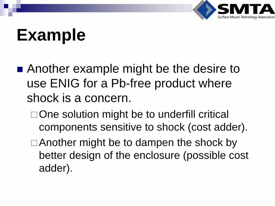
Example
Another example might be the desire to
use ENIG for a Pb-free product where
shock is a concern.
One solution might be to underfill critical
components sensitive to shock (cost adder).
Another might be to dampen the shock by
better design of the enclosure (possible cost
adder).
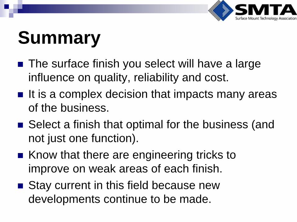
Summary
The surface finish you select will have a large
influence on quality, reliability and cost.
It is a complex decision that impacts many areas
of the business.
Select a finish that optimal for the business (and
not just one function).
Know that there are engineering tricks to
improve on weak areas of each finish.
Stay current in this field because new
developments continue to be made.
Module 4: Printed Circuit Boards
Robustness Concerns
Cracking and Delamination
151
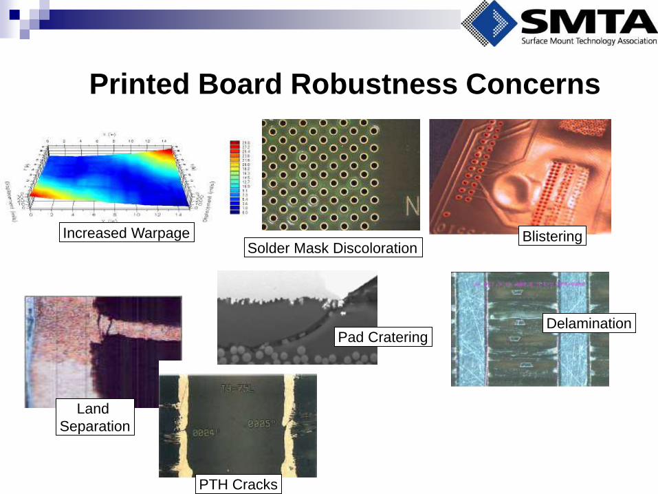
Printed Board Robustness Concerns
Increased Warpage
PTH Cracks
Land
Separation
Solder Mask Discoloration Blistering
Delamination Pad Cratering
Printed Board Damage
• Predicting printed board damage can be difficult • Driven by size (larger boards tend to experience higher
temperatures)
• Driven by thickness (thicker boards experience more thermal stress)
• Driven by material (lower Tg tends to be more susceptible)
• Driven by design (higher density, higher aspect ratios)
• Driven by number of reflows
• No universally accepted industry model
Printed Board Damage: Industry
Response
Concerns with printed board damage
have almost entirely been addressed
through material changes or process
modifications
Not aware of any OEMs initiating design
rules or restrictions
Specific actions driven by board size
and peak temperature requirements
PCB Robustness: Material Selection
The appropriate material selection is
driven by the failure mechanism one is
trying to prevent
Cracking and delamination
Plated through via fatigue
Conductive anodic filament formation
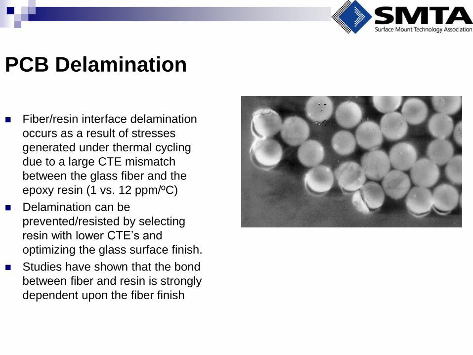
PCB Delamination
Fiber/resin interface delamination
occurs as a result of stresses
generated under thermal cycling
due to a large CTE mismatch
between the glass fiber and the
epoxy resin (1 vs. 12 ppm/ºC)
Delamination can be
prevented/resisted by selecting
resin with lower CTE’s and
optimizing the glass surface finish.
Studies have shown that the bond
between fiber and resin is strongly
dependent upon the fiber finish
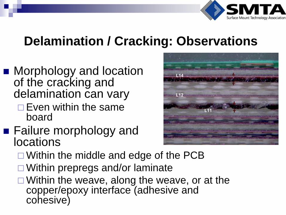
Delamination / Cracking: Observations
Morphology and location of the cracking and delamination can vary Even within the same
board
Failure morphology and locations Within the middle and edge of the PCB
Within prepregs and/or laminate
Within the weave, along the weave, or at the copper/epoxy interface (adhesive and cohesive)

Delamination / Cracking: Root-Cause
Non-Optimized Process Some PCB suppliers have demonstrated improvement
through modifications to lamination process or oxide chemistry
Some observations of lot-to-lot variability
Limit to PCB Capability Difficult to overcome adhesion vs. thermal performance
tradeoff (dicy vs. phenolic)
High stresses developed during Pb-free exceed material strength of standard board material
Moisture Absorption
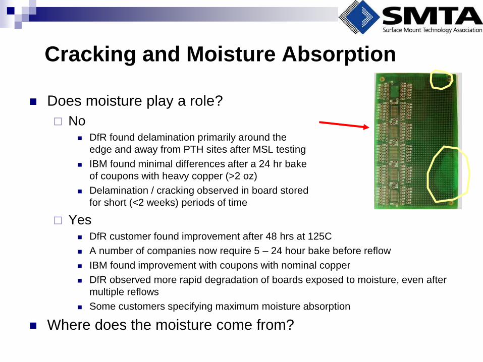
Cracking and Moisture Absorption
Does moisture play a role?
No DfR found delamination primarily around the
edge and away from PTH sites after MSL testing
IBM found minimal differences after a 24 hr bake
of coupons with heavy copper (>2 oz)
Delamination / cracking observed in board stored
for short (<2 weeks) periods of time
Yes DfR customer found improvement after 48 hrs at 125C
A number of companies now require 5 – 24 hour bake before reflow
IBM found improvement with coupons with nominal copper
DfR observed more rapid degradation of boards exposed to moisture, even after
multiple reflows
Some customers specifying maximum moisture absorption
Where does the moisture come from?
Cracking and Moisture (cont.)
Storage of prepregs and laminates
Drilling process
Moisture is absorbed by the side walls
(microcracks?)
Trapped after plating
Storage of PCBs at PCB manufacturer
Storage of PCBs at CCA manufacturer
PCB Trace Peeling
Delamination of trace from surface of the board
Sources of increased stress
Excessive temperatures during high temperature processes
Insufficient curing of resin
Insufficient curing of solder mask
Sources of decreased strength
Improper preparation of copper foil
Excessive undercut
Module 4: Printed Circuit Boards
Plated Through Vias (PTV)
PTH Barrel Cracking
Conductive Anodic Filament (CAF)
162
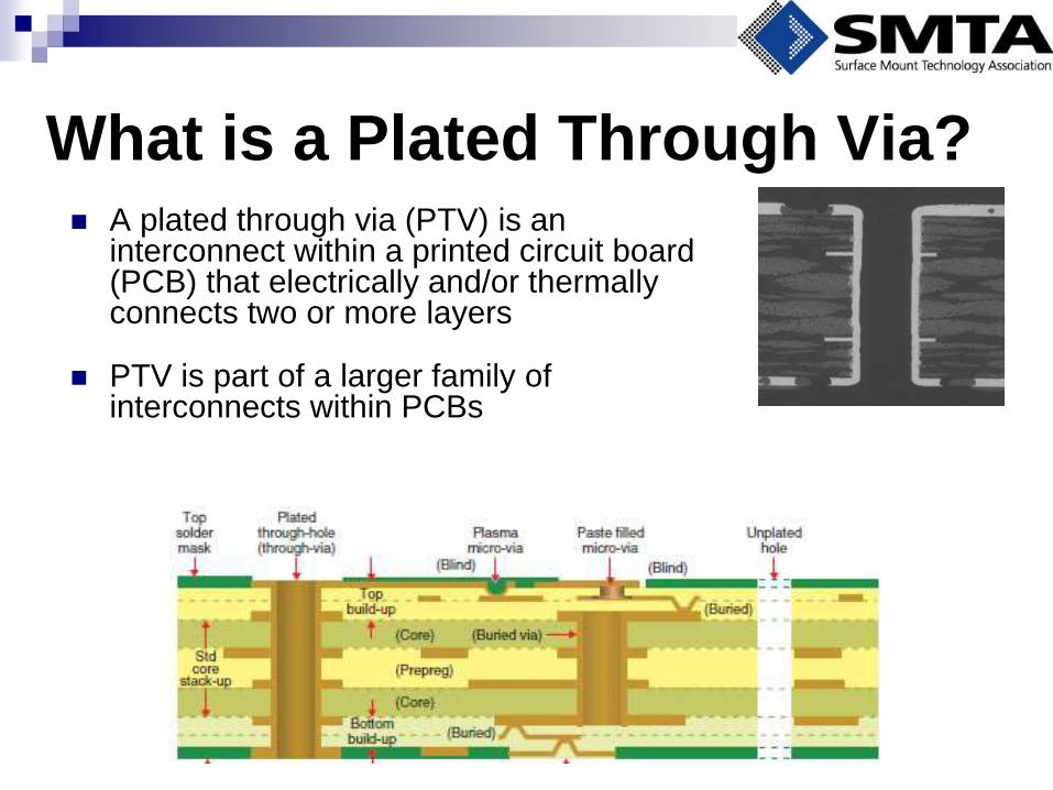
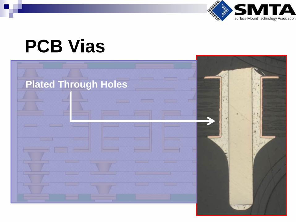
A plated through via (PTV) is an interconnect within a printed circuit board (PCB) that electrically and/or thermally connects two or more layers
PTV is part of a larger family of interconnects within PCBs
What is a Plated Through Via?
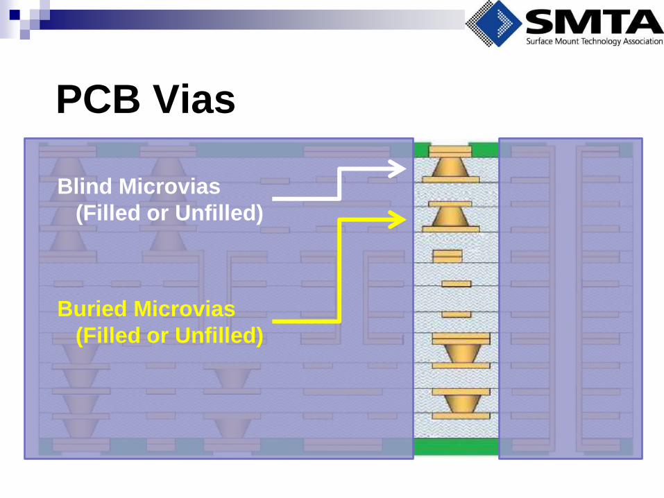
PCB Vias
Blind Microvias
(Filled or Unfilled)
Buried Microvias
(Filled or Unfilled)
PCB Vias
Plated Through Holes
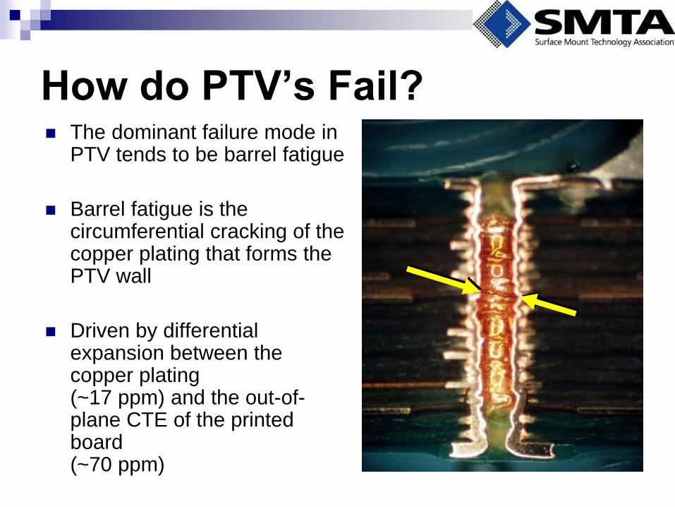
The dominant failure mode in PTV tends to be barrel fatigue
Barrel fatigue is the circumferential cracking of the copper plating that forms the PTV wall
Driven by differential expansion between the copper plating (~17 ppm) and the out-of-plane CTE of the printed board (~70 ppm)
How do PTV’s Fail?
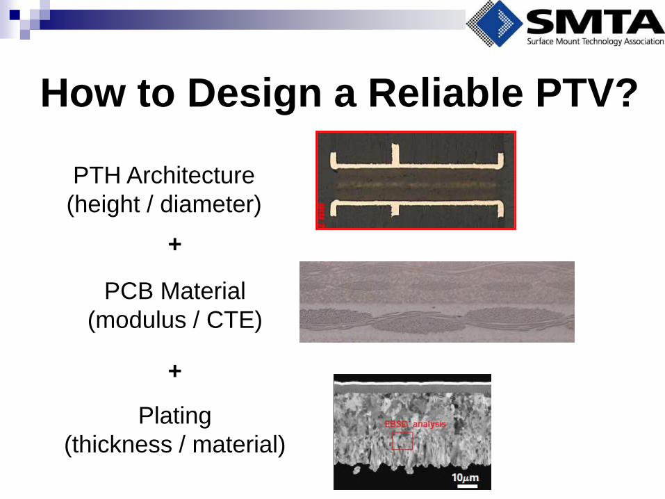
How to Design a Reliable PTV?
PTH Architecture
(height / diameter)
Plating
(thickness / material)
PCB Material
(modulus / CTE)
+
+
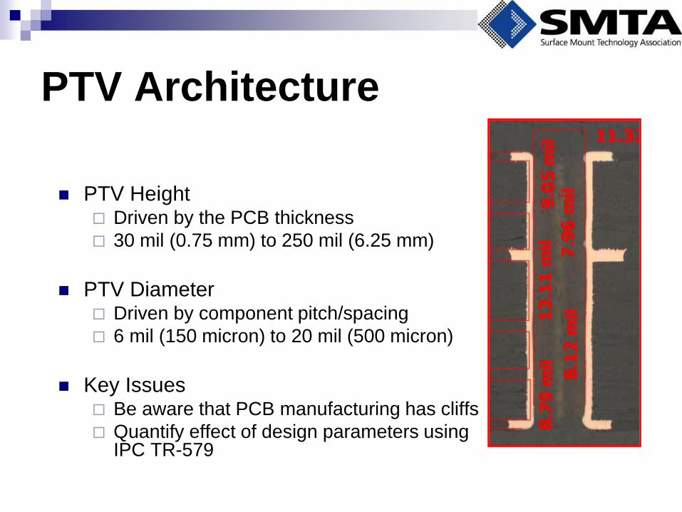
PTV Height Driven by the PCB thickness
30 mil (0.75 mm) to 250 mil (6.25 mm)
PTV Diameter Driven by component pitch/spacing
6 mil (150 micron) to 20 mil (500 micron)
Key Issues Be aware that PCB manufacturing has cliffs
Quantify effect of design parameters using IPC TR-579
PTV Architecture
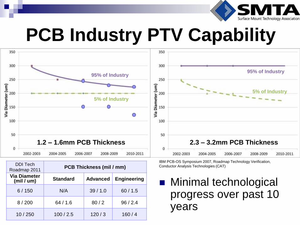
Minimal technological progress over past 10 years
PCB Industry PTV Capability
2.3 – 3.2mm PCB Thickness
95% of Industry
5% of Industry
1.2 – 1.6mm PCB Thickness
95% of Industry
5% of Industry
DDI Tech
Roadmap 2011 PCB Thickness (mil / mm)
Via Diameter (mil / um) Standard Advanced Engineering
6 / 150 N/A 39 / 1.0 60 / 1.5
8 / 200 64 / 1.6 80 / 2 96 / 2.4
10 / 250 100 / 2.5 120 / 3 160 / 4
IBM PCB-OS Symposium 2007, Roadmap Technology Verification,
Conductor Analysis Technologies (CAT)
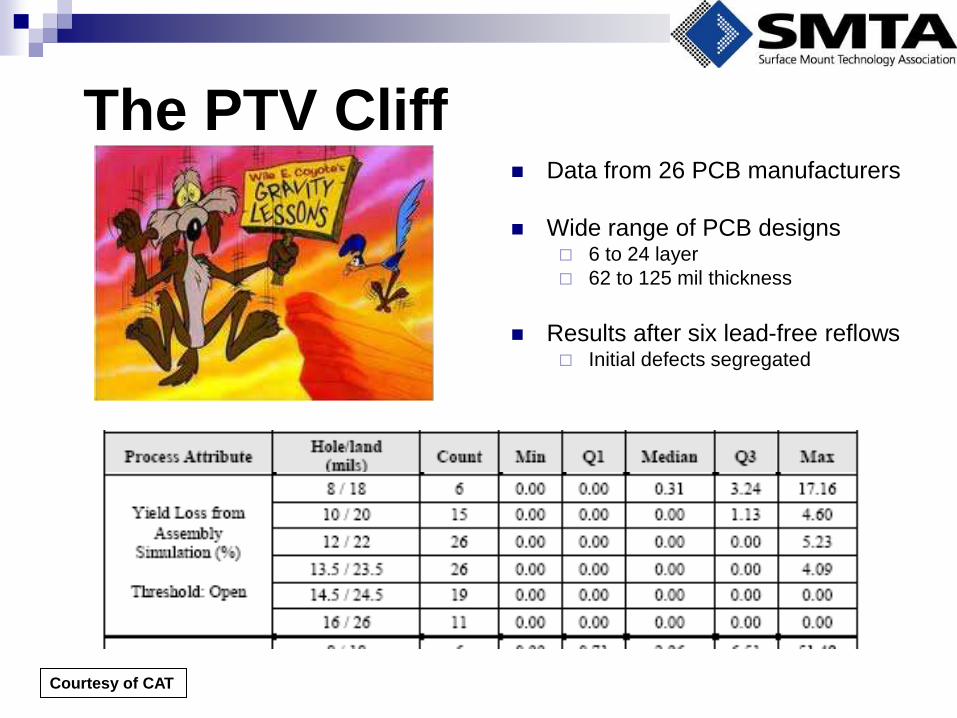
Data from 26 PCB manufacturers
Wide range of PCB designs 6 to 24 layer
62 to 125 mil thickness
Results after six lead-free reflows Initial defects segregated
The PTV Cliff
Courtesy of CAT

Round Robin Reliability Evaluation of Small Diameter (<20 mil) Plated Through Holes in PWBs
Activity initiated by IPC and published in 1988
Objectives Confirm sufficient reliability
Benchmark different test procedures
Evaluate influence of PTH design and plating (develop a model)
IPC TR-579
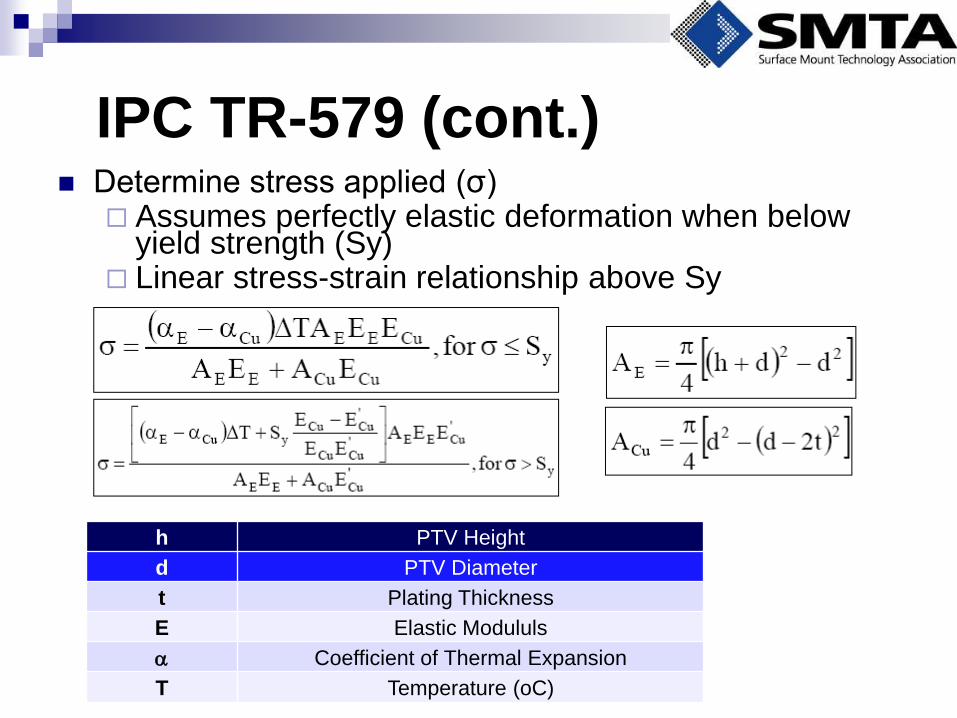
IPC TR-579 (cont.) Determine stress applied (σ)
Assumes perfectly elastic deformation when below yield strength (Sy)
Linear stress-strain relationship above Sy
h PTV Height
d PTV Diameter
t Plating Thickness
E Elastic Modululs
Coefficient of Thermal Expansion
T Temperature (oC)
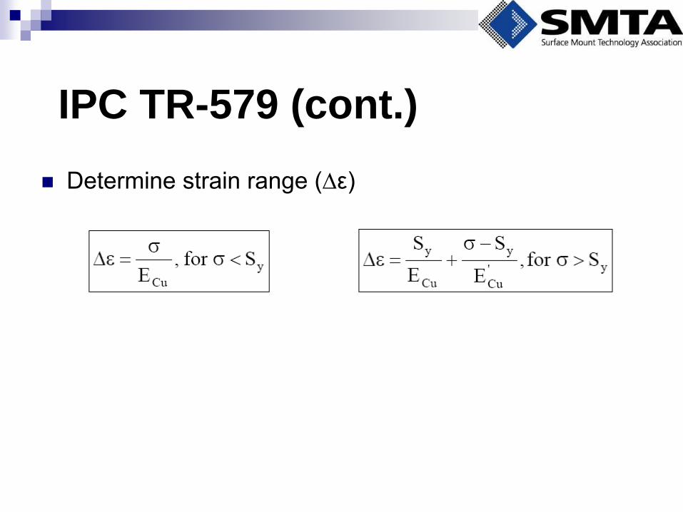
IPC TR-579 (cont.)
Determine strain range (∆ε)
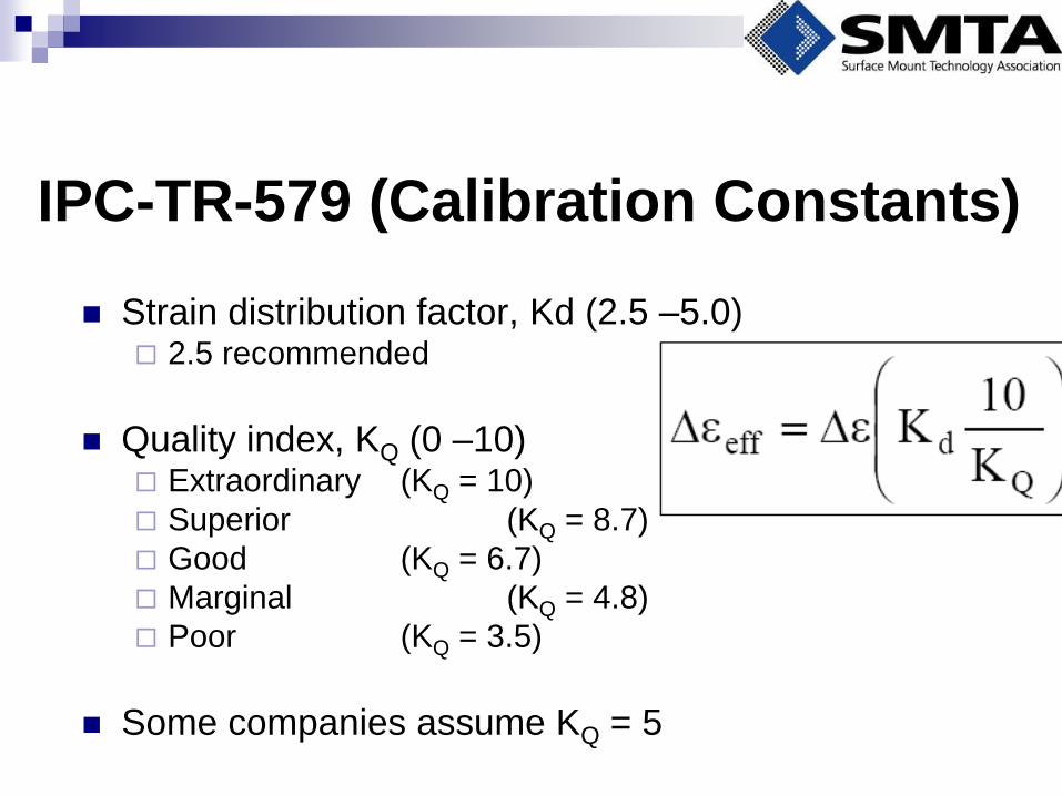
IPC-TR-579 (Calibration Constants)
Strain distribution factor, Kd (2.5 –5.0) 2.5 recommended
Quality index, KQ (0 –10) Extraordinary (KQ = 10)
Superior (KQ = 8.7)
Good (KQ = 6.7)
Marginal (KQ = 4.8)
Poor (KQ = 3.5)
Some companies assume KQ = 5

IPC TR-579 (cont.)
Iteratively calculate cycles-to-failure (Nf)
Df Elongation (assumed ~30%)
Su Tensile Strength (assumed ~40,000
psi)
Two key plating properties
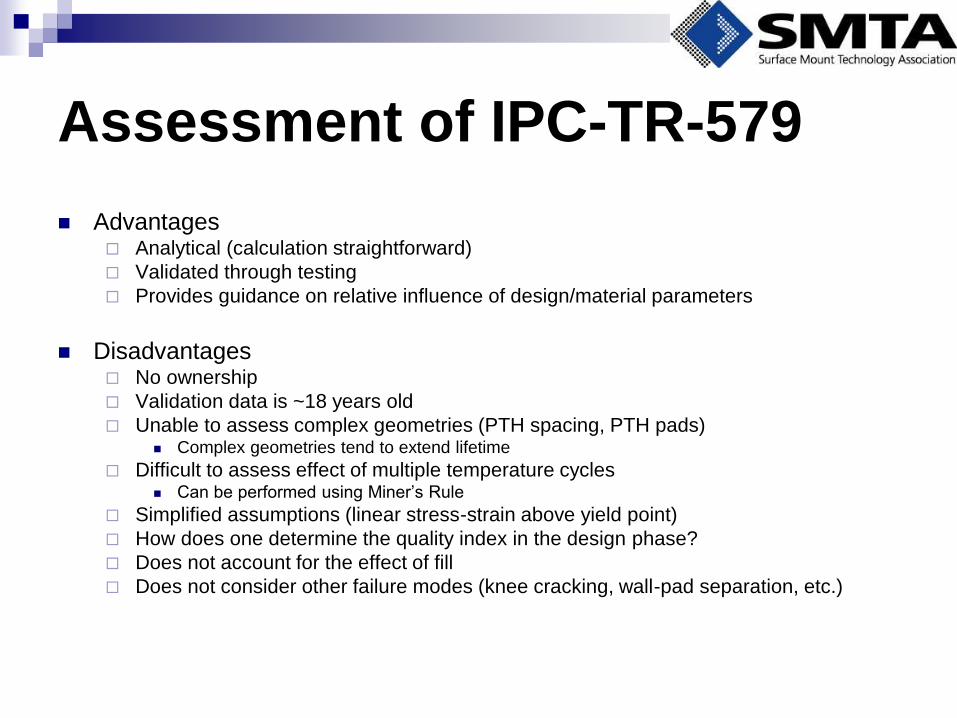
Advantages Analytical (calculation straightforward)
Validated through testing
Provides guidance on relative influence of design/material parameters
Disadvantages No ownership
Validation data is ~18 years old
Unable to assess complex geometries (PTH spacing, PTH pads) Complex geometries tend to extend lifetime
Difficult to assess effect of multiple temperature cycles Can be performed using Miner’s Rule
Simplified assumptions (linear stress-strain above yield point)
How does one determine the quality index in the design phase?
Does not account for the effect of fill
Does not consider other failure modes (knee cracking, wall-pad separation, etc.)
Assessment of IPC-TR-579
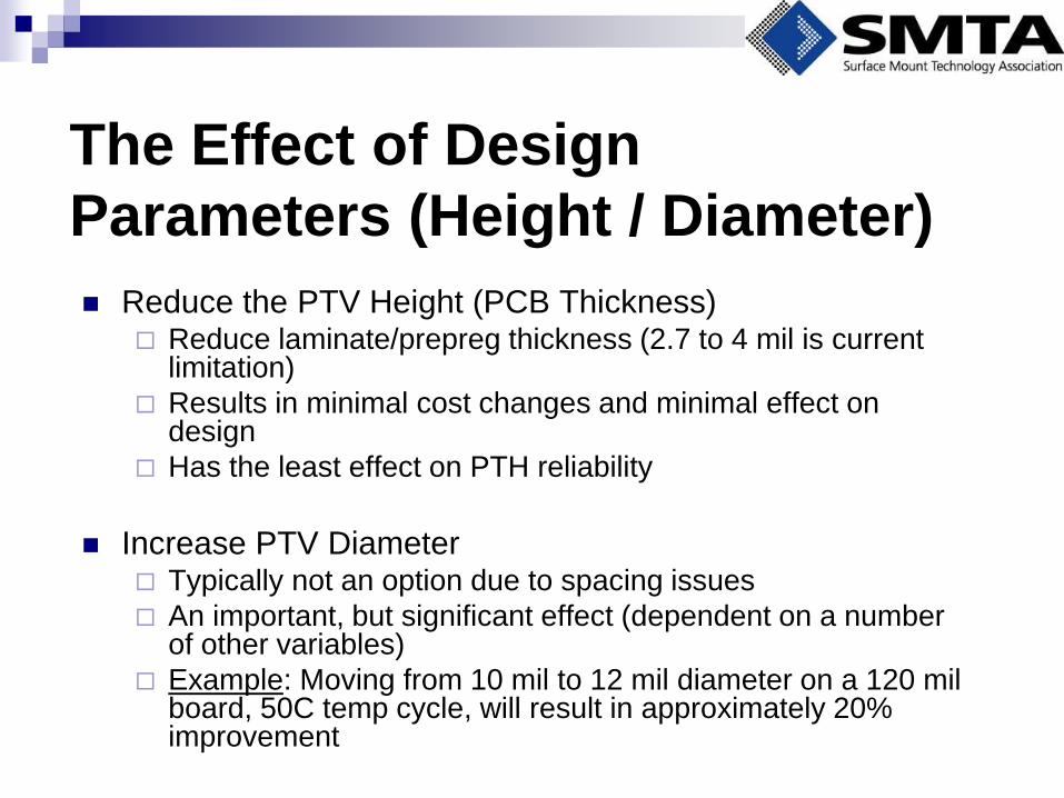
Reduce the PTV Height (PCB Thickness) Reduce laminate/prepreg thickness (2.7 to 4 mil is current
limitation)
Results in minimal cost changes and minimal effect on design
Has the least effect on PTH reliability
Increase PTV Diameter Typically not an option due to spacing issues
An important, but significant effect (dependent on a number of other variables)
Example: Moving from 10 mil to 12 mil diameter on a 120 mil board, 50C temp cycle, will result in approximately 20% improvement
The Effect of Design
Parameters (Height / Diameter)
Effect of Design Parameters (cont.)
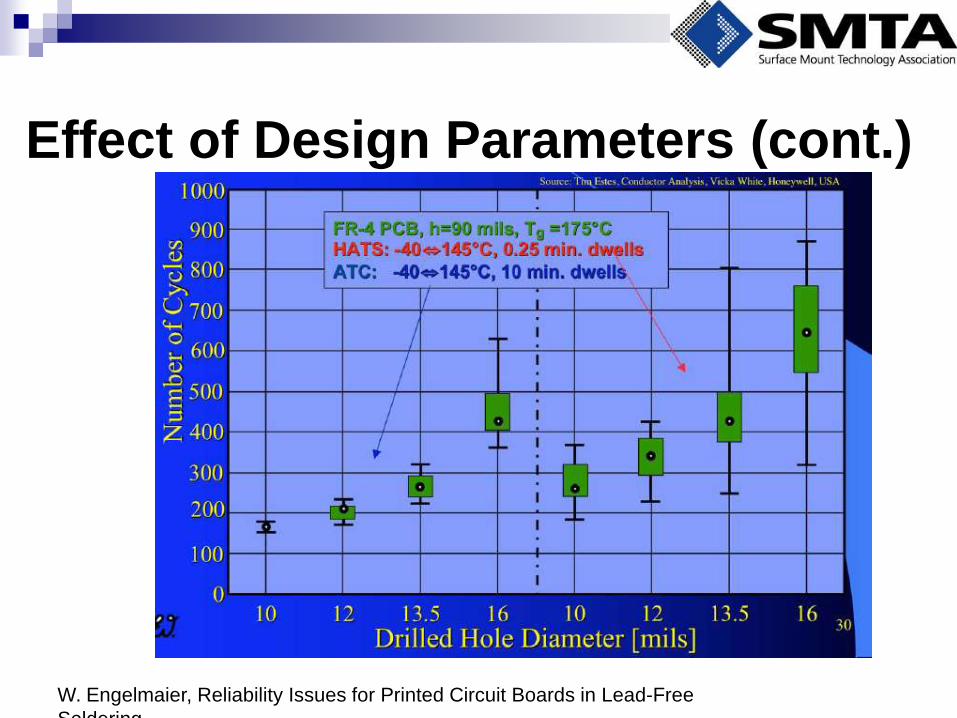
W. Engelmaier, Reliability Issues for Printed Circuit Boards in Lead-Free
Soldering
S. Neumann, Theoretical and Practical Aspects of Thermo Mechanical Reliability in Printed Circuit Boards
with Copper Plated Through Holes
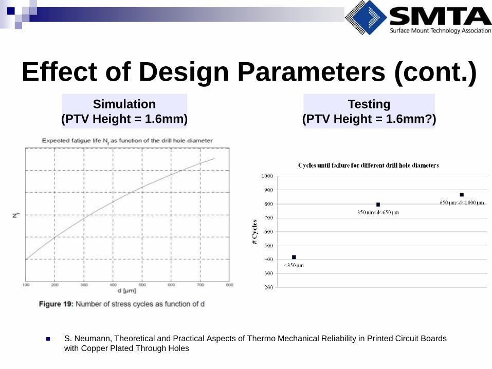
Effect of Design Parameters (cont.) Simulation
(PTV Height = 1.6mm)
Testing
(PTV Height = 1.6mm?)
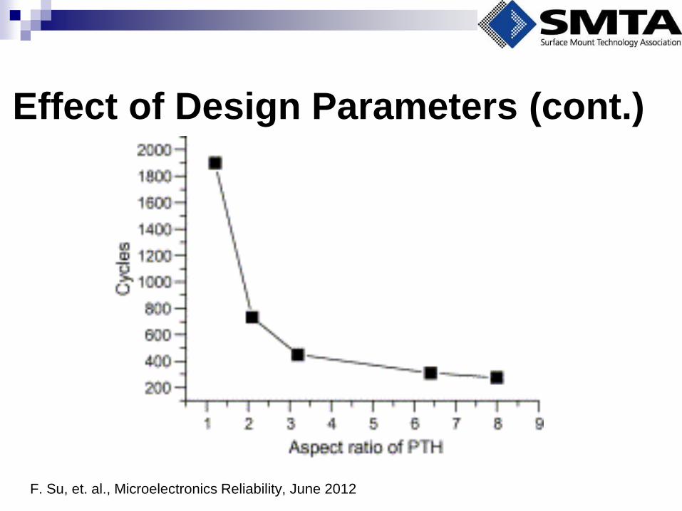
F. Su, et. al., Microelectronics Reliability, June 2012
Effect of Design Parameters (cont.)
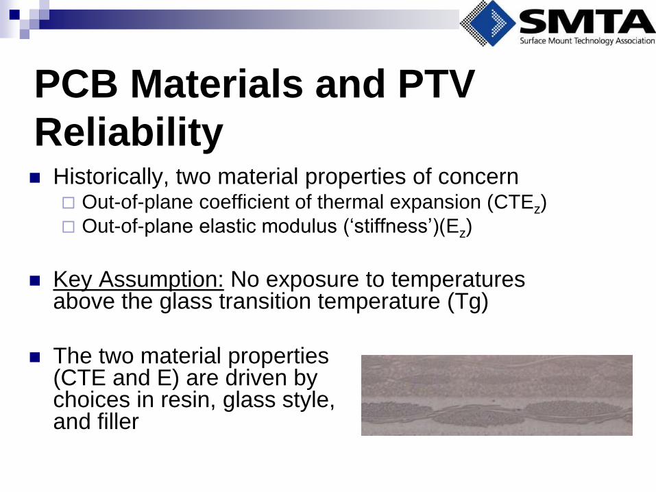
Historically, two material properties of concern Out-of-plane coefficient of thermal expansion (CTEz)
Out-of-plane elastic modulus (‘stiffness’)(Ez)
Key Assumption: No exposure to temperatures above the glass transition temperature (Tg)
The two material properties (CTE and E) are driven by choices in resin, glass style, and filler
PCB Materials and PTV
Reliability
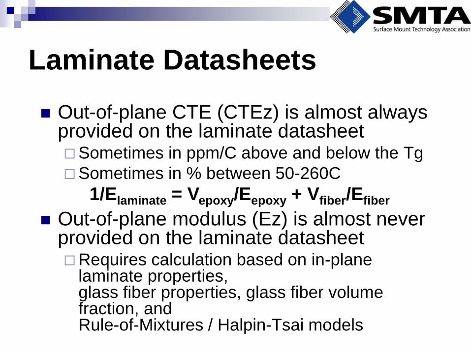
Out-of-plane CTE (CTEz) is almost always provided on the laminate datasheet Sometimes in ppm/C above and below the Tg
Sometimes in % between 50-260C
Out-of-plane modulus (Ez) is almost never provided on the laminate datasheet Requires calculation based on in-plane
laminate properties, glass fiber properties, glass fiber volume fraction, and Rule-of-Mixtures / Halpin-Tsai models
Laminate Datasheets
1/Elaminate = Vepoxy/Eepoxy + Vfiber/Efiber
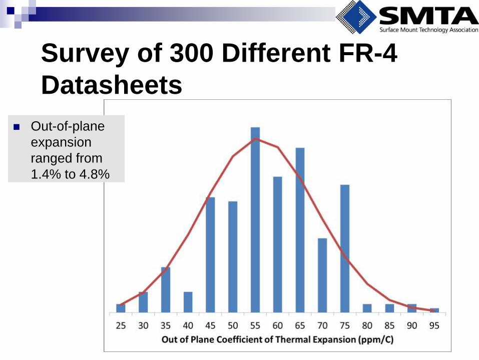
Survey of 300 Different FR-4
Datasheets
Out-of-plane
expansion
ranged from
1.4% to 4.8%

PCB laminates (and prepregs) are fabricated with a variety of glass styles
Problem: All datasheet properties are for laminate with 7628 glass style
Most laminate (and all prepreg) in complex PCBs have a low volume fraction of glass (i.e., 1080 or 106)
Glass Style Glass
Style
Resin
Volume
Content
Fiber
Volume
Content
1027 0.86 0.14
1037 0.86 0.14
106 0.84 0.16
1067 0.84 0.16
1035 0.83 0.17
1078 0.82 0.18
1080 0.79 0.21
1086 0.78 0.22
2313 0.74 0.26
2113 0.72 0.28
2116 0.71 0.29
3313 0.71 0.29
3070 0.68 0.32
1647 0.66 0.34
1651 0.66 0.34
2165 0.66 0.34
2157 0.66 0.34
7628 0.64 0.36
Glass Style and CTE Glass Style Modulus of Elasticity Ez (MPa) CTEz (ppm)
1027 4380.4 73.9
1037 4380.4 73.9
106 4478.2 72.3
1067 4478.2 72.3
1035 4528.7 71.5
1078 4580.3 70.7
1080 4742.7 68.4
1086 4799.3 67.6
2313 5040.4 64.4
2113 5170.2 62.8
2116 5237.6 62.0
3313 5237.6 62.0
3070 5450.9 59.7
1647 5603.1 58.1
1651 5603.1 58.1
2165 5603.1 58.1
2157 5603.1 58.1
7628 5764.0 56.5
More recently, additional laminate properties of concern due to Pb-free assembly Glass transition temperature (Tg)
Time to delamination (T260, T280, T288, T300)
Temperature of decomposition (Td)
Each parameter ‘supposedly’ captures a different material behavior Higher number slash sheets (> 100) within IPC-4101
define these parameters to specific material categories
Laminate Properties (cont.)
Glass transition temperature (Tg) (IPC-TM-650, 2.4.24/2.4.25c) Characterizes complex material transformation
(increase in CTE, decrease in modulus)
Time to delamination (T-260/280/288/300) (IPC-TM-650, 2.4.24.1) Characterizes interfacial adhesion
Temperature of decomposition (Td) (IPC-TM-650, 2.3.40) Characterizes breakdown of epoxy material
Thermal Parameters of
Laminate
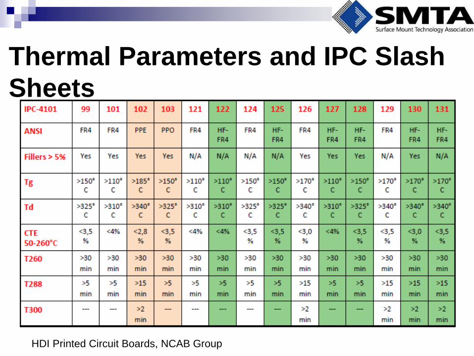
HDI Printed Circuit Boards, NCAB Group
Thermal Parameters and IPC Slash
Sheets
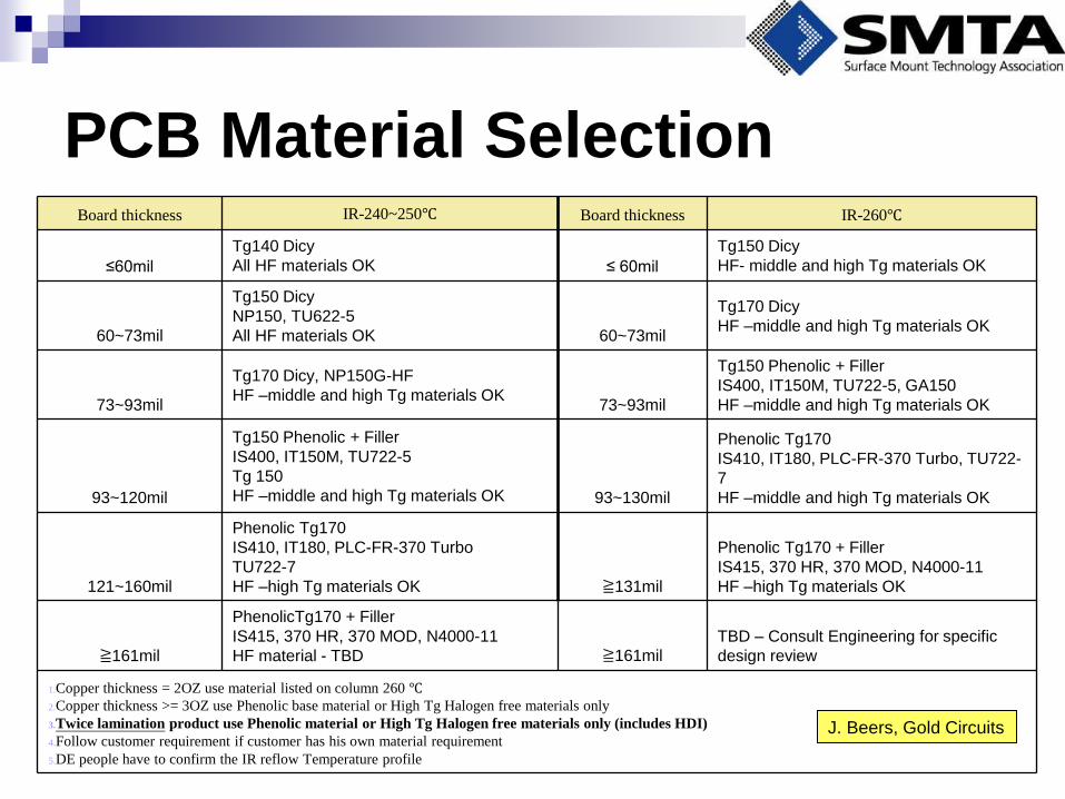
189
PCB Material Selection Board thickness IR-240~250 Board thickness IR-260
≤60mil
Tg140 Dicy
All HF materials OK ≤ 60mil
Tg150 Dicy
HF- middle and high Tg materials OK
60~73mil
Tg150 Dicy
NP150, TU622-5
All HF materials OK 60~73mil
Tg170 Dicy
HF –middle and high Tg materials OK
73~93mil
Tg170 Dicy, NP150G-HF
HF –middle and high Tg materials OK 73~93mil
Tg150 Phenolic + Filler
IS400, IT150M, TU722-5, GA150
HF –middle and high Tg materials OK
93~120mil
Tg150 Phenolic + Filler
IS400, IT150M, TU722-5
Tg 150
HF –middle and high Tg materials OK 93~130mil
Phenolic Tg170
IS410, IT180, PLC-FR-370 Turbo, TU722-
7
HF –middle and high Tg materials OK
121~160mil
Phenolic Tg170
IS410, IT180, PLC-FR-370 Turbo
TU722-7
HF –high Tg materials OK ≧131mil
Phenolic Tg170 + Filler
IS415, 370 HR, 370 MOD, N4000-11
HF –high Tg materials OK
≧161mil
PhenolicTg170 + Filler
IS415, 370 HR, 370 MOD, N4000-11
HF material - TBD ≧161mil
TBD – Consult Engineering for specific
design review
1.Copper thickness = 2OZ use material listed on column 260
2.Copper thickness >= 3OZ use Phenolic base material or High Tg Halogen free materials only
3.Twice lamination product use Phenolic material or High Tg Halogen free materials only (includes HDI)
4.Follow customer requirement if customer has his own material requirement
5.DE people have to confirm the IR reflow Temperature profile
J. Beers, Gold Circuits
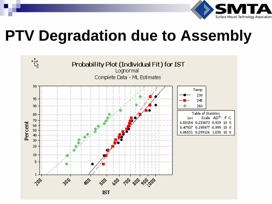
PTV Degradation due to Assembly
190
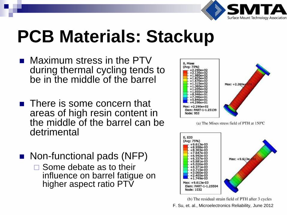
Maximum stress in the PTV during thermal cycling tends to be in the middle of the barrel
There is some concern that areas of high resin content in the middle of the barrel can be detrimental
Non-functional pads (NFP) Some debate as to their
influence on barrel fatigue on higher aspect ratio PTV
PCB Materials: Stackup
F. Su, et. al., Microelectronics Reliability, June 2012
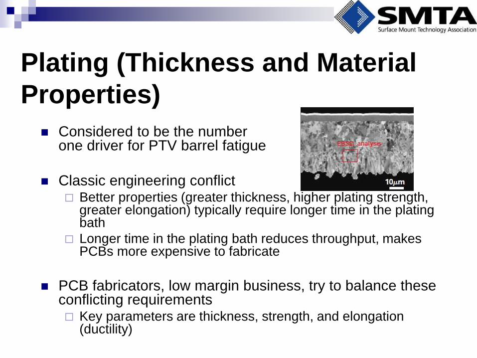
Considered to be the number one driver for PTV barrel fatigue
Classic engineering conflict Better properties (greater thickness, higher plating strength,
greater elongation) typically require longer time in the plating bath
Longer time in the plating bath reduces throughput, makes PCBs more expensive to fabricate
PCB fabricators, low margin business, try to balance these conflicting requirements Key parameters are thickness, strength, and elongation
(ductility)
Plating (Thickness and Material
Properties)
Specifications tend to range from 0.8 mil (20 microns) to 1.0 mil (25 microns) to 1.2 mil (30 microns)
Plating thickness can be less of an issue than previously
New formulations to fill microvias can drive an accelerated plating process Some PCB manufacturers, depending on the design and
production volume, will plate the PTV almost closed
Plating Thickness
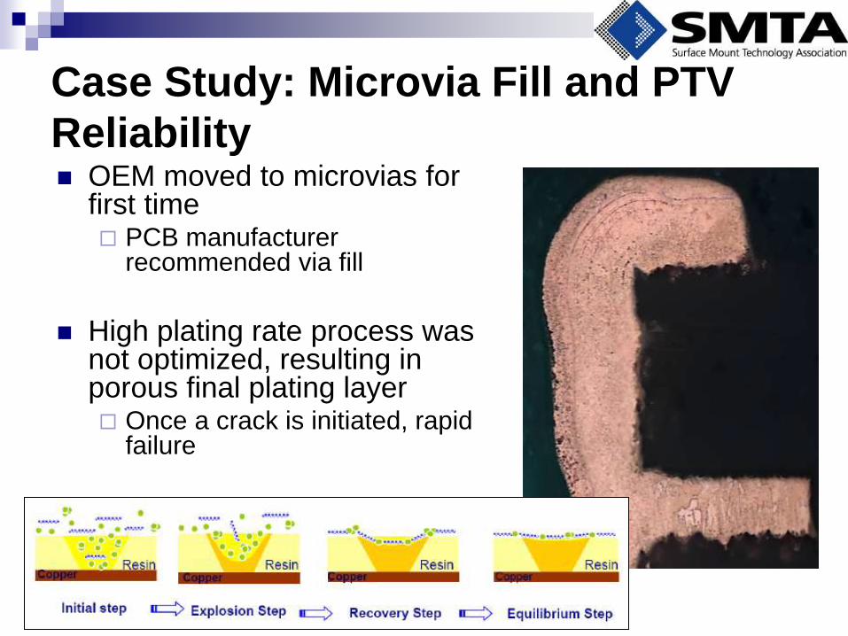
OEM moved to microvias for first time PCB manufacturer
recommended via fill
High plating rate process was not optimized, resulting in porous final plating layer Once a crack is initiated, rapid
failure
Case Study: Microvia Fill and PTV
Reliability
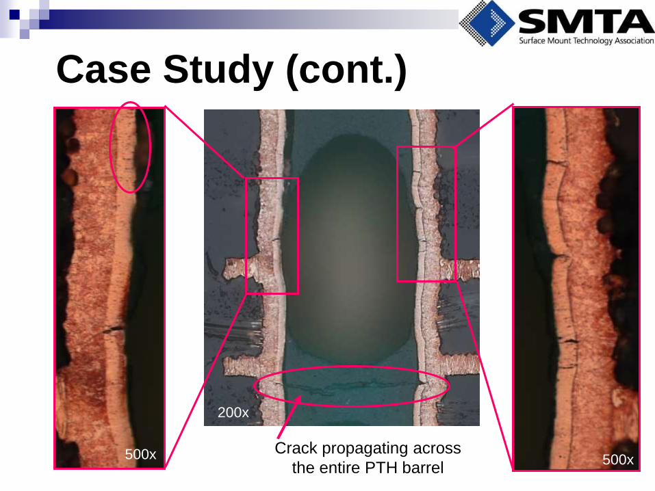
Case Study (cont.)
200x
500x 500x Crack propagating across
the entire PTH barrel

Industry Requirements (IPC-6012C) Ultimate Tensile Strength 36,000 psi (250 MPa)
Elongation 12%
Plating Mechanical Properties
Controlled measurements
from 26 different plating baths
(Top 25 PCB manufacturer)
PCB Manufacturers tend to be very
aware of test requirements specified by
larger/higher rel customers
Plating conditions are adjusted to meet the
test requirements of those industries /
customers
The Reality of PTV
Performance (cont.)
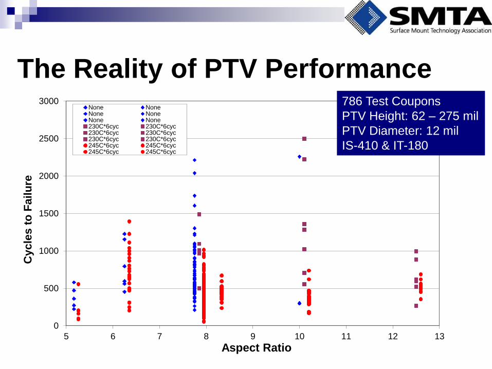
The Reality of PTV Performance
0
500
1000
1500
2000
2500
3000
5 6 7 8 9 10 11 12 13
Cy
cle
s t
o F
ail
ure
Aspect Ratio
None NoneNone NoneNone None230C*6cyc 230C*6cyc230C*6cyc 230C*6cyc230C*6cyc 230C*6cyc245C*6cyc 245C*6cyc245C*6cyc 245C*6cyc
786 Test Coupons
PTV Height: 62 – 275 mil
PTV Diameter: 12 mil
IS-410 & IT-180
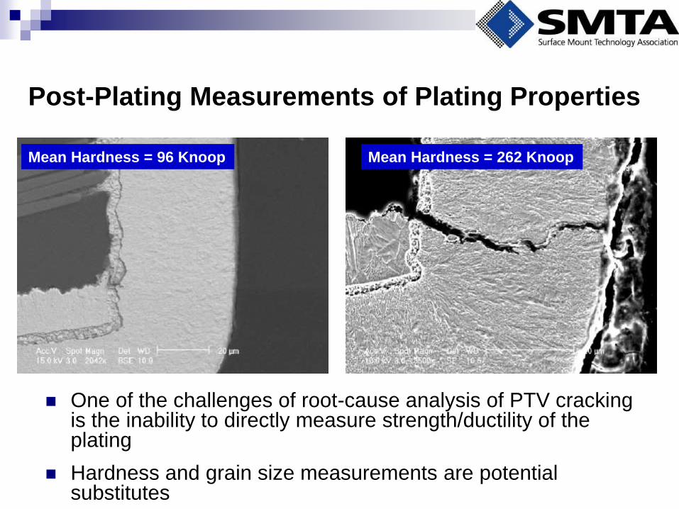
Mean Hardness = 96 Knoop
One of the challenges of root-cause analysis of PTV cracking is the inability to directly measure strength/ductility of the plating
Hardness and grain size measurements are potential substitutes
Post-Plating Measurements of Plating Properties
Mean Hardness = 262 Knoop
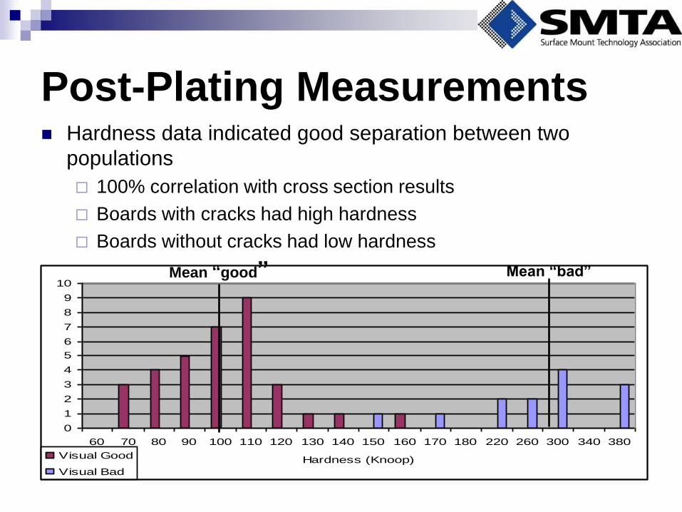
Post-Plating Measurements Hardness data indicated good separation between two
populations
100% correlation with cross section results
Boards with cracks had high hardness
Boards without cracks had low hardness
0
1
2
3
4
5
6
7
8
9
10
60 70 80 90 100 110 120 130 140 150 160 170 180 220 260 300 340 380
Hardness (Knoop)Visual Good
Visual Bad
Mean “good” Mean “bad”
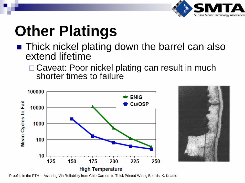
Thick nickel plating down the barrel can also extend lifetime Caveat: Poor nickel plating can result in much
shorter times to failure
Other Platings
Proof is in the PTH -- Assuring Via Reliability from Chip Carriers to Thick Printed Wiring Boards, K. Knadle
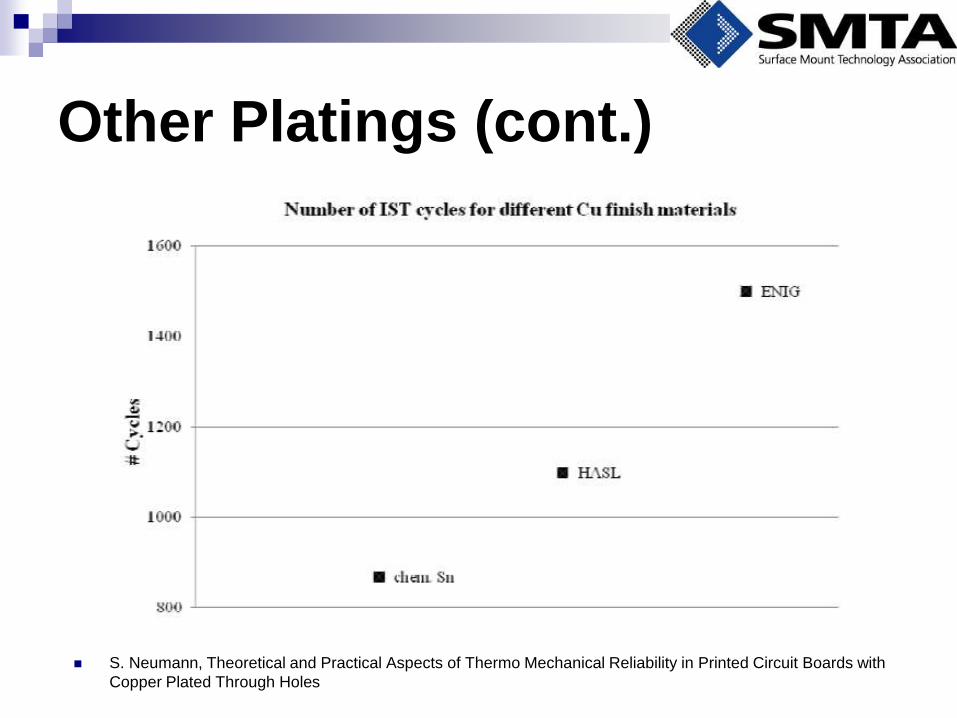
S. Neumann, Theoretical and Practical Aspects of Thermo Mechanical Reliability in Printed Circuit Boards with
Copper Plated Through Holes
Other Platings (cont.)
There are currently six procedures for testing/qualifying a PTV Modeling and simulation
Cross-sectioning + solder float/shock
Thermal shock testing (also thermal cycling)
Interconnect stress testing (IST)
Printed Board Process Capability, Quality, and Relative Reliability (PCQR2)
Highly Accelerated Thermal Shock (HATS)
What does DfR recommend?
How to Test/Qualify a Reliable
PTV?
Qualifying PTV is a two-step process
The first step is to qualify the design and the PCB manufacturer Initial qualification
The second step is to initiate ongoing testing to monitor outgoing quality Lot qualification
Test / Qualify PTV
Qualify the design through simulation / modeling
DfR has implemented IPC TR-579 into our Automated Design Analysis software, Sherlock, to allow for rapid assessment of PTV robustness
First step: Define the environment (test or field or both)
Initial Qualification
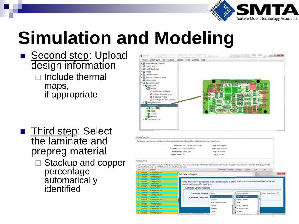
Second step: Upload design information Include thermal
maps, if appropriate
Third step: Select the laminate and prepreg material Stackup and copper
percentage automatically identified
Simulation and Modeling
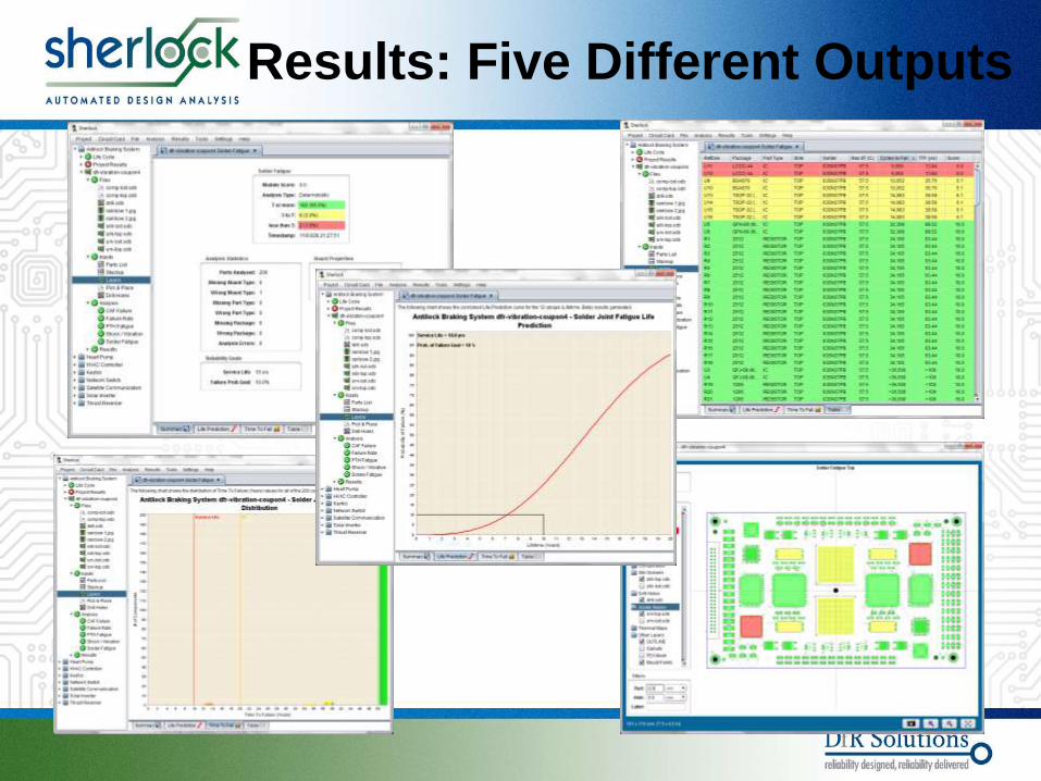
Results: Five Different Outputs
Qualify the design and manufacturer through PCQR2 Consists of a coupon design, a test standard, and a
database
18″ x 24″ layout with 1″ x 1″ test modules (352)
2 – 24 layers (rigid, rigid-flex)
Three panels / three non-consecutive lots
Simulated assembly (6X) and thermal cycling (HATS)
Initial Qualification (PCQR2)
Advantages Industry standard (IPC-9151)
Plug and play
Provides real data for understanding of PCB supplier capabilities and comparison to the rest of the industry through the use of an anonymous database
Disadvantages Industry-certified monopoly
$2K - $5K, not including panel costs
PCQR2 (cont.)
Interconnect stress testing (IST) is the overwhelming favorite of high reliability organizations Small (1 x 4) coupon can fit along the edge of the panel
Testing is automated
Widely used
Ability to drive barrel fatigue and post separation
Large number of holes (up to 300) and continuous resistance monitoring makes it far superior to cross-sectioning And it should be cheaper!
Lot Qualification
Coupon design is critical (IST can be prone to problems)
Need to specify preconditioning (IST or real reflow oven?)
Need to specify frequency (every lot, every month, every quarter)
Need to specify maximum temperature (some debate on the validity of results when above the Tg) 130, 150, and 175C are the most common
Need to specify requirements Different markets/organizations specify different times to
failure (300, 500, and 1000 cycles are most common)
IST – Issues / Awareness
The base knowledge and understanding of PTV Fatigue is robust Decades of testing and simulation
Use of reliability physics is best practice
Detailed understanding is still missing Key expertise (process parameters, material properties, simulation,
testing) is rarely in the same organization
Not a pure science activity (significant amount of human influence)
Improvements in out-of-plane CTE and plating properties have greatly improved PTV performance Avoiding defects continues to be the biggest risk
Conclusion
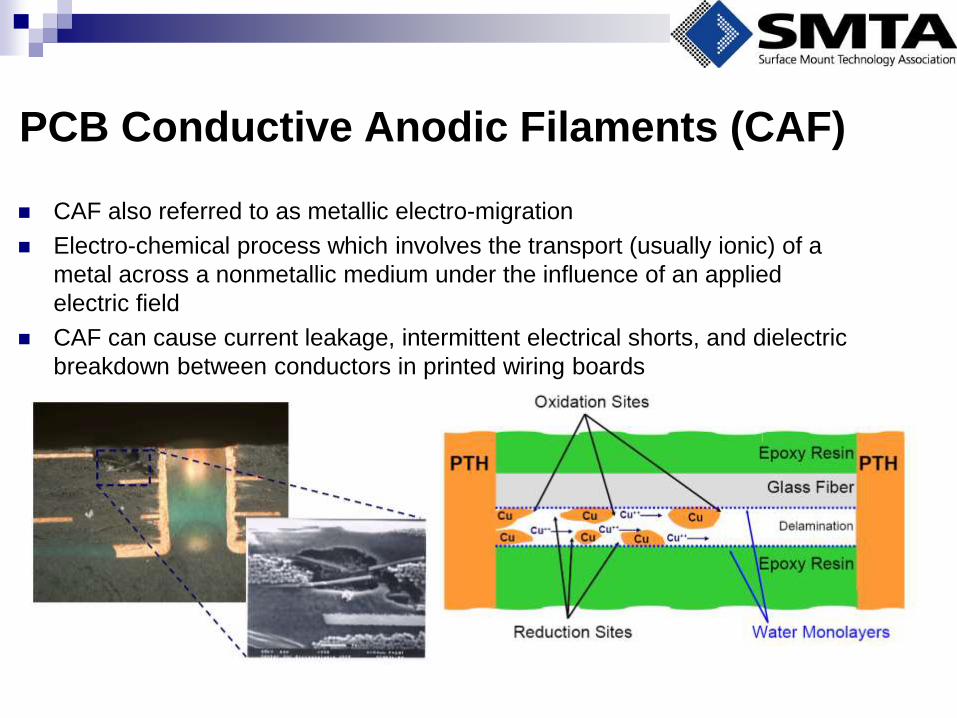
PCB Conductive Anodic Filaments (CAF)
CAF also referred to as metallic electro-migration
Electro-chemical process which involves the transport (usually ionic) of a
metal across a nonmetallic medium under the influence of an applied
electric field
CAF can cause current leakage, intermittent electrical shorts, and dielectric
breakdown between conductors in printed wiring boards
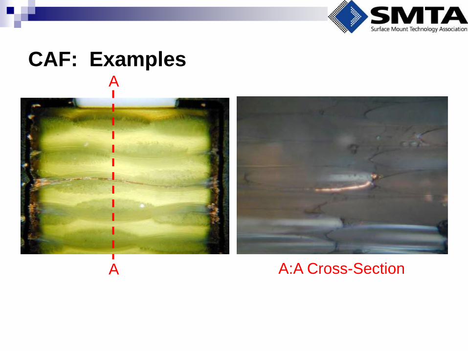
214
CAF: Examples A
A A:A Cross-Section
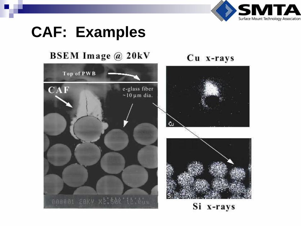
CAF: Examples
Module 4: Printed Circuit Boards Strain Flexure Issues & Pad Cratering Cleanliness
Electro-Chemical Migration (ECM)
216

SAC Solder is More Vulnerable to Strain
PCB deflection
Ten
sile
fo
rce o
n
pad
an
d L
am
inate
PbSn
LF
PbSn limit LF limit
Laminate Load
Bearing
Capability
Loa
d (kN
)
0.1
0.15
0.2
0.25
0.3
0.35
0.4
0.45
0.5
SAC Sn-Pb
Solder Alloy
Each Pair
Student's t
0.05
SAC
Sn-Pb
Level
18
18
Number
0.230859
0.416101
Mean
0.056591
0.040408
Std Dev
0.01334
0.00952
Std Err Mean
0.20272
0.39601
Lower 95%
0.25900
0.43620
Upper 95%
Means and Std Dev iations
Onew ay Analysis of Load (kN) By Solder Alloy
NEMI study showed SAC is more
Sensitive to bend stress. Sources of strain can be ICT, stuffing
through-hole components,
shipping/handling, mounting to a chassis,
or shock events.
Strain & Flexure: Pad Cratering
o Cracking initiating within the laminate during a
dynamic mechanical event
o In circuit testing (ICT), board depanelization, connector
insertion, shock and vibration, etc.
G. Shade, Intel (2006)
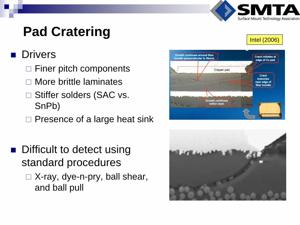
Pad Cratering
Drivers
Finer pitch components
More brittle laminates
Stiffer solders (SAC vs.
SnPb)
Presence of a large heat sink
Difficult to detect using
standard procedures
X-ray, dye-n-pry, ball shear,
and ball pull
Intel (2006)
220
Potential Mitigations to Pad Cratering
• Design
• Non-critical pads
• Solder mask defined vs. non-solder mask defined
• Pad Geometry
• Layout & PCB thickness
• Limitations on board flexure
• 750 to 500 microstrain, component and layout dependent
• Process Control & Validation
• Corner Glue
• More compliant solder
• SAC305 is relatively rigid, SAC105 and SNC are possible
alternatives
• New laminate acceptance criteria and materials

Component Supplier Practices
Intel Example
• Pad design influences failure
• Smaller pads result in higher stress under
a given load
• Solder mask defined pads can provide
additional strength
• Increases tolerable strain
• But, moves failure location from pad crater
to intermetallic fracture
Pad Geometry
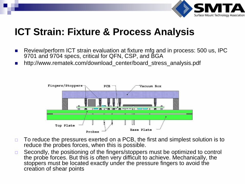
Review/perform ICT strain evaluation at fixture mfg and in process: 500 us, IPC 9701 and 9704 specs, critical for QFN, CSP, and BGA
http://www.rematek.com/download_center/board_stress_analysis.pdf
To reduce the pressures exerted on a PCB, the first and simplest solution is to reduce the probes forces, when this is possible.
Secondly, the positioning of the fingers/stoppers must be optimized to control the probe forces. But this is often very difficult to achieve. Mechanically, the stoppers must be located exactly under the pressure fingers to avoid the creation of shear points
ICT Strain: Fixture & Process Analysis
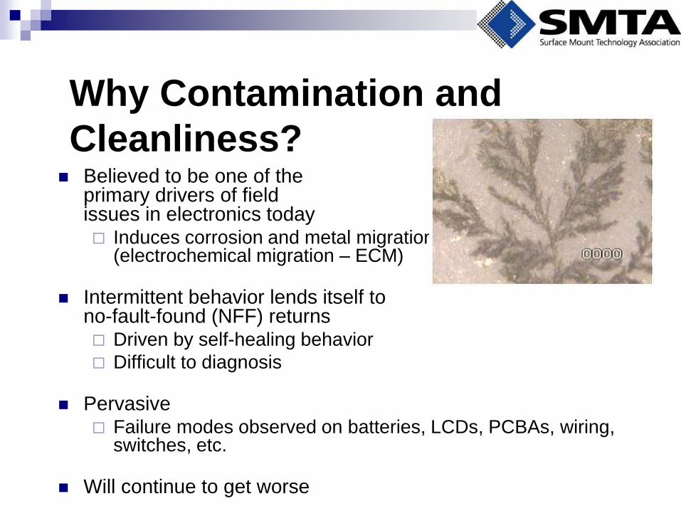
Why Contamination and
Cleanliness? Believed to be one of the
primary drivers of field issues in electronics today Induces corrosion and metal migration
(electrochemical migration – ECM)
Intermittent behavior lends itself to no-fault-found (NFF) returns Driven by self-healing behavior
Difficult to diagnosis
Pervasive Failure modes observed on batteries, LCDs, PCBAs, wiring,
switches, etc.
Will continue to get worse
Future of Contamination / Cleanliness
Continued reductions in pitch between conductors will make future packaging more susceptible
Increased use of leadless packages (QFN, land grid array, etc.) results in reduction in standoff
Will reduce efficiency of cleaning, which may lead to increased concentration of contaminants
Increased product sales into countries with polluted and tropical environments (East Asia, South Asia, etc.)
ECM occurrence very sensitive to ambient humidity conditions
Pb-Free and smaller bond pads
Require more aggressive flux formulations

The Future: Reduced Spacings Critical distance effect?
Two studies by DfR staff NaCl seeding
Conformal coating over no-clean flux residues
Over 300 coupons tested (IPC-B-25) 6.25, 12.5, and 25 mil spacings; 40C/93%RH, 65C/88%RH,
85C/85%RH
No ECM at 25 mil spacings
Experience based on older designs may not be valid
Test coupons must have the same spacing and same electric field as actual product
Parameter Spacing
Peripheral Flip Chip Solder
Bumps 5 mil (120 mm)
Thin Shrink Small Outline
Package (TSSOP) Leads 7 mil (170 mm)
PCB External Traces (low
voltage line) 4 mil (100 mm)
BGA Substrate Traces 2 mil (48 mm)
Failure Mode
Why do you care about excessive
contamination or insufficient cleanliness?
Electrochemical Migration (note: not Electromigration; completely different mechanism)
Understanding the mechanism provides
insight into the drivers and appropriate
mitigations
Electrochemical Migration
(ECM)
Defined, per IPC-TR-476A,
Electrochemical Migration: Electrically
Induced Failures in Printed Wiring
Assemblies (1997), as
“The growth of conductive metal filaments
or dendrites on or through a printed board
under the influence of a DC voltage bias”
Too narrow
What is ECM?
Alternative definition
Movement of metal through an electrolytic solution under
an applied electric field between insulated conductors
Electrochemical migration can occur on or in almost
all electronic packaging
Die surface
Epoxy encapsulant
Printed board
Passive components
Etc.
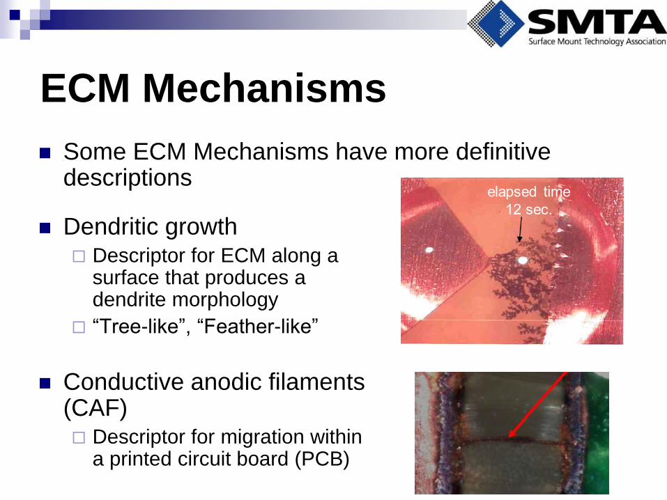
ECM Mechanisms
Some ECM Mechanisms have more definitive descriptions
Dendritic growth Descriptor for ECM along a
surface that produces a dendrite morphology
“Tree-like”, “Feather-like”
Conductive anodic filaments (CAF) Descriptor for migration within
a printed circuit board (PCB)
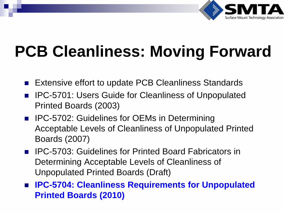
PCB Cleanliness: Moving Forward
Extensive effort to update PCB Cleanliness Standards
IPC-5701: Users Guide for Cleanliness of Unpopulated
Printed Boards (2003)
IPC-5702: Guidelines for OEMs in Determining
Acceptable Levels of Cleanliness of Unpopulated Printed
Boards (2007)
IPC-5703: Guidelines for Printed Board Fabricators in
Determining Acceptable Levels of Cleanliness of
Unpopulated Printed Boards (Draft)
IPC-5704: Cleanliness Requirements for Unpopulated
Printed Boards (2010)
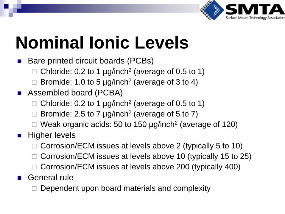
Nominal Ionic Levels Bare printed circuit boards (PCBs)
Chloride: 0.2 to 1 µg/inch2 (average of 0.5 to 1)
Bromide: 1.0 to 5 µg/inch2 (average of 3 to 4)
Assembled board (PCBA)
Chloride: 0.2 to 1 µg/inch2 (average of 0.5 to 1)
Bromide: 2.5 to 7 µg/inch2 (average of 5 to 7)
Weak organic acids: 50 to 150 µg/inch2 (average of 120)
Higher levels
Corrosion/ECM issues at levels above 2 (typically 5 to 10)
Corrosion/ECM issues at levels above 10 (typically 15 to 25)
Corrosion/ECM issues at levels above 200 (typically 400)
General rule
Dependent upon board materials and complexity
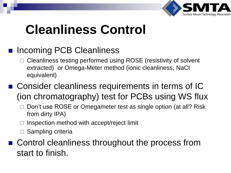
Cleanliness Control
Incoming PCB Cleanliness Cleanliness testing performed using ROSE (resistivity of solvent
extracted) or Omega-Meter method (ionic cleanliness, NaCl
equivalent)
Consider cleanliness requirements in terms of IC
(ion chromatography) test for PCBs using WS flux Don’t use ROSE or Omegameter test as single option (at all? Risk
from dirty IPA)
Inspection method with accept/reject limit
Sampling criteria
Control cleanliness throughout the process from
start to finish.
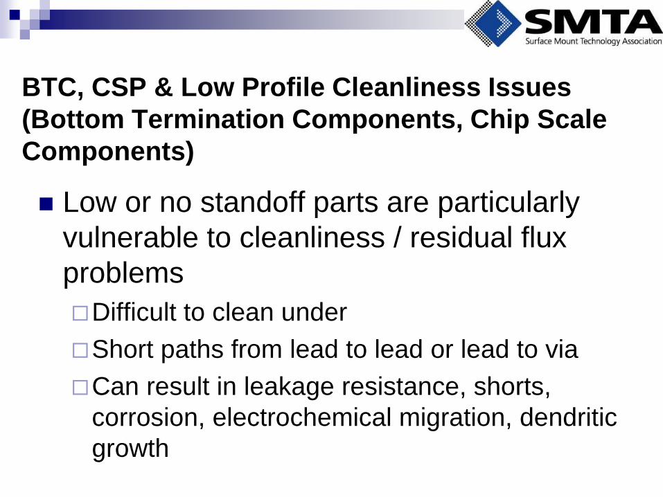
BTC, CSP & Low Profile Cleanliness Issues
(Bottom Termination Components, Chip Scale
Components)
Low or no standoff parts are particularly
vulnerable to cleanliness / residual flux
problems
Difficult to clean under
Short paths from lead to lead or lead to via
Can result in leakage resistance, shorts,
corrosion, electrochemical migration, dendritic
growth
Recommendations – Process
Qualification
Validate compatibility of all new process
materials using SIR testing. Under revisions now: IPC-B-52 SIR TEST VEHICLE
Continue spot check testing of cleanliness using
ion chromatography under low profile SMT parts
Summary
To avoid design mistakes, be aware that
functionality is just the beginning. Design
reliability in!
Be aware of industry best practices
Maximize knowledge of your design as early in
the product development process as possible
Practice design for excellence (DfX)
Design for manufacturability
Design for sourcing
Design for reliability
Design for environment

Conclusions
Design for Reliability is a valuable process for
lowering cost, reducing time-to-market, and
improving customer satisfaction
PoF is a powerful tool that can leverage the
value of DfR activities
Successful DfR / PoF implementation requires
the right combination of personnel and tools and
time limitations
Contact Information
• Questions?
• Contact Greg Caswell,
301-640-5825
• 443-834-9284 (cell)
• www.dfrsolutions.com
• Connect with me on LinkedIn as well!

Presenter Biography
Greg has over 40 years of experience in electronics manufacturing focusing on failure analysis and reliability. He is passionate about applying his unique background to enable his clients to maximize and accelerate product design and development while saving time, managing resources, and improving customer satisfaction.
Greg, a Senior Member of the Technical Staff for DfR Solutions, is an industry recognized expert in the fields of SMT, advanced packaging, printed board fabrication, circuit card assembly, and bonding solutions using nanotechnology. He has been well-regarded as a leader in the electronics contract manufacturing and component packaging industries for the past 40 years. Prior to joining DfR Greg was the Vice President of Engineering at Reactive Nanotechnology (RNT), where he led application development for the RNT Nanofoil® and ensured a successful transition of product technology to Indium Corporation. His previous appointments include Vice President of Business Development for Newport Enterprises, Director of Engineering for VirTex Assembly Services, and Technical Director at Silicon Hills Design. He has presented over 250 papers at conferences all over the world and has taught courses at IMAPS, SMTA and IPC events. He helped design the 1st pick and place system used exclusively for SMT in 1978, edited and co-authored the 1st book on SMT in 1984 for ISHM and built the 1st SMT electronics launched into space.
B.A., Management (St. Edwards University)
B.S., Electrical Engineering (Rutgers University)
239