design guidelines ceramic component design
TRANSCRIPT

Chap Section § FolioCC 015 02 1
EGIDE SA EGIDE USASite Industriel Sactar - CS20205 4 Washington Street84505 Bollène - France 21613 Cambridge, MD - USAPhone +33 4 90 30 97 11 Phone +1 410 901 6100
W.Muffato F.Disperati F.Benkoussa
DESIGN GUIDE LINE FOR CERAMIC PACKAGE
Title : CERAMIC COMPONENT DESIGN
Production15/11/2016
QualityApprovalApproval
Last Issue Date :
By : M.WILL
Established By :Previous Issue Date : 26/06/2016
Creation : 18/03/2003JF LECOEUCHE
TechnicalApproval
Ce document est la propriété d’Egide. Toute reproduction interdite sans autorisation écrite préalable.
This document is the property of Egide. Any reproduction prohibited without preliminary written authorization
DESIGN GUIDELINES
CERAMIC COMPONENT DESIGN
EGIDE CONFIDENTIAL

Chap Section § FolioCC 015 02 2
Package Drawing on a file format describe on the table belowTechnical Specification (PDF or Word format)
Routing Data should be at least compose by this following documents :- Routing on Gerber format 274X w/embedded apertures - Routing on DXF (1 file per layer)
Required Data for Each Layer :- Design of the Ceramic Cavity (Design of the Tape)- Design of the Conductors- Vias coming from the underneath layer
Data required for verification :- Net List on Excel Spreadsheet- Net Key on PDF- Net Key on DXF
We could read the following format:
Hardcopy
GERBER 274D w/aperture list
EGIDE CONFIDENTIALCe document est la propriété d’Egide. Toute reproduction interdite sans autorisation écrite préalable.
This document is the property of Egide. Any reproduction prohibited without preliminary written authorization
Solidworks format
IGES
Title : CERAMIC COMPONENT DESIGN
DRAWING FILE 3D FILE
AutoCad DWG formatAutoCad DXF format (preferred)
This section can be use as a guide during the design phase of the ceramic component. Weindicate the standard data we generally apply, we also indicate our process limit. As eachproduct has his own characteristics, we encourage you to contact your Sales Representative todiscuss about your project and help you on the design phase.
Solidworks format
AutoCad DXF formatSTEP
INTRODUCTION
REQUIRED DATA
ARTWORK FILEGERBER 274X w/embedded apertures
COMPUTER FILES FORMATS
AutoCad DWG format AutoCad DWG format
PDF (preferred) SATBMP
DESIGN GUIDE LINE FOR CERAMIC PACKAGE
Solidworks format

Chap Section § FolioCC 015 02 3
44444444
6
7777
88888
99999
10101010
1111111111
1212
Surface Distance External Edge to Conductors T
DD
CD
H
J
E
EGIDE CONFIDENTIAL
A
DESIGN GUIDE LINE FOR CERAMIC PACKAGE
Title : CERAMIC COMPONENT DESIGN
X
Ce document est la propriété d’Egide. Toute reproduction interdite sans autorisation écrite préalable.
INDEX
SheetParameterDesignation
Y
Internal Via Cover Pad U
LVia Centerline to External Edge M
Via Centerline to Cavity Edge (Upper Layer)
BLength of the Package
f
Via Centerline to Cavity Edge (Same Layer) K
Surface Line Space RSurface Distance Cavity to Conductor S
Internal Line Space W
Distance Internal Conductor to Cavity Upper LayerDistance Surface Conductor to Cavity Upper Layer
Internal Distance External Edge to Conductors
This document is the property of Egide. Any reproduction prohibited without preliminary written authorization
Leadless Chip Carrier
Width of the PackageLength of the CavityWidth of the Cavity
BB
Internal Line Width V
NP
Internal Distance Cavity to Conductor
Pad Array - Long Grid Array
Pad Misalignment
Ground Plane Clearance to Via Cover Pad
Ground Plane Clearance to External EdgeGround Plane Clearance to Cavity
Internal Tie Bar Connexion WidthInternal Tie Bar Pitch between Connexion
EE
GG
ZAA
CC
FF
HH
G
Via Diameter
Cavity RadiusCeramic Overall ThicknessCeramic Tape Thickness
Ceramic Flatness
F
Via Centerline Pitch
Surface Via Cover PadSurface Line Width
Bonding Pad Pull Back
Chap Section § FolioCC 015 02 4
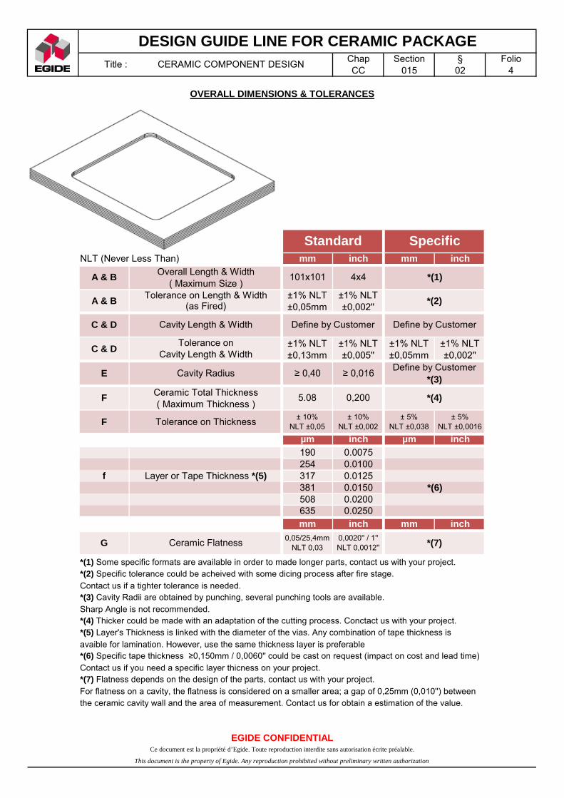
NLT (Never Less Than) mm inch mm inch
µm inch µm inch
190 0.0075254 0.0100
f 317 0.0125381 0.0150508 0.0200635 0.0250mm inch mm inch
*(1) Some specific formats are available in order to made longer parts, contact us with your project.*(2) Specific tolerance could be acheived with some dicing process after fire stage.
Contact us if a tighter tolerance is needed.*(3) Cavity Radii are obtained by punching, several punching tools are available.
Sharp Angle is not recommended.*(4) Thicker could be made with an adaptation of the cutting process. Conctact us with your project.*(5) Layer's Thickness is linked with the diameter of the vias. Any combination of tape thickness is
avaible for lamination. However, use the same thickness layer is preferable*(6) Specific tape thickness ≥0,150mm / 0,0060'' could be cast on request (impact on cost and lead time)
Contact us if you need a specific layer thicness on your project.*(7) Flatness depends on the design of the parts, contact us with your project.
For flatness on a cavity, the flatness is considered on a smaller area; a gap of 0,25mm (0,010'') betweenthe ceramic cavity wall and the area of measurement. Contact us for obtain a estimation of the value.
Title : CERAMIC COMPONENT DESIGN
FCeramic Total Thickness 5.08
Cavity Length & Width
0,05/25,4mm NLT 0,03
0,0020'' / 1'' NLT 0,0012''
Ce document est la propriété d’Egide. Toute reproduction interdite sans autorisation écrite préalable.
G
This document is the property of Egide. Any reproduction prohibited without preliminary written authorization
± 5%NLT ±0,0016
Layer or Tape Thickness *(5)
± 10%NLT ±0,002
± 5%NLT ±0,038
*(6)
± 10%NLT ±0,05
C & D
Tolerance on Thickness
EGIDE CONFIDENTIAL
*(7)Ceramic Flatness
DESIGN GUIDE LINE FOR CERAMIC PACKAGE
F
OVERALL DIMENSIONS & TOLERANCES
±1% NLT ±0,005''
101x101
0,200
Cavity Length & Width
(as Fired)
A & B
( Maximum Thickness )
≥ 0,40
Define by Customer Define by Customer
Cavity Radius
Overall Length & Width( Maximum Size )
*(4)
±1% NLT ±0,002''
±1% NLT ±0,05mm
≥ 0,016Define by Customer
*(3)
Specific
4x4
Standard
E
A & B
C & DTolerance on ±1% NLT
±0,13mm
Tolerance on Length & Width
*(1)
±1% NLT ±0,05mm
±1% NLT ±0,002''
*(2)

Chap Section § FolioCC 015 02 5
EGIDE CONFIDENTIAL
CERAMIC COMPONENT DESIGN
DESIGN GUIDE LINE FOR CERAMIC PACKAGE
Title :
Ce document est la propriété d’Egide. Toute reproduction interdite sans autorisation écrite préalable.
This document is the property of Egide. Any reproduction prohibited without preliminary written authorization
Chap Section § FolioCC 015 02 6
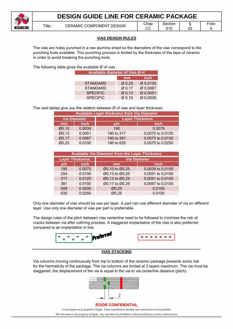
The vias are holes punched in a raw alumina sheet so the diameters of the vias correspond to thepunching tools available. This punching process is limited by the thickness of the tape of ceramicin order to avoid breaking the punching tools.
The following table gives the available Ø of vias :
mm inch
Ø 0,25 Ø 0,0100Ø 0,17 Ø 0,0067Ø 0,13 Ø 0,0051Ø 0,10 Ø 0,0039
The next tables give you the relation between Ø of vias and layer thickness:
mm inchØ0,10 0.0039Ø0,13 0.0051Ø0,17 0.0067Ø0,25 0.0100
µm inch190 0.0075254 0.0100317 0.0125381 0.0150508 0.0200635 0.0250
Only one diameter of vias should be use per layer. A part can use different diameter of via on differentlayer. Use only one diameter of vias per part is preferrable.
The design rules of the pitch between vias centerline need to be followed to minimize the risk ofcracks between via after cofirring process. A staggered implantation of the vias is also preferredcompared to an implantation in line.
Via columns moving continuously from top to bottom of the ceramic package presents some risk for the hermeticity of the package. The via columns are limited at 3 layers maximum. The via must bestaggered, the displacement of the via is equal to the via to via centerline distance (pitch).
inch0,0039 to 0,01000,0051 to 0,01000,0051 to 0,0100
Ø0,17 to Ø0,25
VIAS STACKING
Ø0,13 to Ø0,25Ø0,13 to Ø0,25
This document is the property of Egide. Any reproduction prohibited without preliminary written authorization
Ø0,25
DESIGN GUIDE LINE FOR CERAMIC PACKAGE
190 to 381 0,0075 to 0,0150190 to 317
0,0075 to 0,0250
CERAMIC COMPONENT DESIGN
STANDARD
0,0075 to 0,0125
SPECIFICSPECIFIC
Layer Thickness
Layer Thickness Via Diameter
EGIDE CONFIDENTIAL
0.0100Ø0,25
190 to 635
0,0067 to 0,01000,0100
Ø0,10 to Ø0,25
VIAS DESIGN RULES
Title :
Available diameter of Vias Ø H
Ce document est la propriété d’Egide. Toute reproduction interdite sans autorisation écrite préalable.
Via Diameter
STANDARD
mm
190µm
Available Via Diameter from the Layer Thickness
Available Layer thickness from Via Diameter
inch0.0075
Chap Section § FolioCC 015 02 7
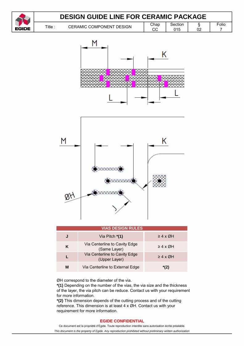
ØH correspond to the diameter of the via.*(1) Depending on the number of the vias, the via size and the thicknessof the layer, the via pitch can be reduce. Contact us with your requirementfor more information.*(2) This dimension depends of the cutting process and of the cuttingreference. This dimension is at least 4 x ØH. Contact us with yourrequirement for more information.
*(2)
≥ 4 x ØH
≥ 4 x ØH
≥ 4 x ØH
VIAS DESIGN RULES
This document is the property of Egide. Any reproduction prohibited without preliminary written authorization
CERAMIC COMPONENT DESIGN
M
Via Centerline to Cavity Edge(Upper Layer)
K
J Via Pitch *(1)
DESIGN GUIDE LINE FOR CERAMIC PACKAGE
EGIDE CONFIDENTIALCe document est la propriété d’Egide. Toute reproduction interdite sans autorisation écrite préalable.
Title :
L
Via Centerline to External Edge
Via Centerline to Cavity Edge(Same Layer)

Chap Section § FolioCC 015 02 8
mm inch mm inch0.25 0,0100 ≥0,50 ≥0,0200.17 0,0067 ≥0,35 ≥0,0140.13 0,0051 ≥0,25 ≥0,0100.10 0,0039 ≥0,25 ≥0,010
mm inch mm inch
P ≥ 0,20 ≥ 0,008 ≥ 0,10 ≥ 0,004R ≥ 0,20 ≥ 0,008 ≥ 0,10 ≥ 0,004S ≥ 0,25 ≥ 0,010 ≥ 0,20 ≥ 0,008
Dimensions of Metallization for Brazed Component is taken in charge by Egide.Design with the maximum gap between two conductors is preferred
SURFACE LAYER DESIGN
Via Diameter (ØH) Via Cover Pad (ØN)
STANDARD SPECIFIC
Line WidthLine Spaces
Edge to ConductorDepends of the cutting process & of the cutting
reference / Contact us with your project
DESIGN GUIDE LINE FOR CERAMIC PACKAGE
Cavity to Conductor
Title :
T
Ce document est la propriété d’Egide. Toute reproduction interdite sans autorisation écrite préalable.
This document is the property of Egide. Any reproduction prohibited without preliminary written authorization
CERAMIC COMPONENT DESIGN
EGIDE CONFIDENTIAL

Chap Section § FolioCC 015 02 9
mm inch mm inch0.25 0,0100 ≥0,30 ≥0,0120.17 0,0067 ≥0,30 ≥0,0120.13 0,0051 ≥0,22 ≥0,0090.10 0,0039 ≥0,22 ≥0,009
mm inch mm inch mm inch
V ≥ 0,15 ≥ 0,006 ≥ 0,10 ≥ 0,004 ≥ 0,075 ≥ 0,003W ≥ 0,15 ≥ 0,006 ≥ 0,10 ≥ 0,004 ≥ 0,075 ≥ 0,003X ≥ 0,25 ≥ 0,010 ≥ 0,20 ≥ 0,008
Design with the maximum gap between two conductors is preferred
SPECIFIC LOCALLY
Depends of the cutting process & of the cutting reference / Contact us with your project
CERAMIC COMPONENT DESIGN
Via Diameter (ØH) Via Cover Pad (ØU)
DESIGN GUIDE LINE FOR CERAMIC PACKAGE
Title :
Ce document est la propriété d’Egide. Toute reproduction interdite sans autorisation écrite préalable.
This document is the property of Egide. Any reproduction prohibited without preliminary written authorization
INTERNAL LAYER DESIGN
STANDARD SPECIFIC
Line WidthLine Spaces
Cavity to Conductor
Y Edge to Conductor
EGIDE CONFIDENTIAL

Chap Section § FolioCC 015 02 10
Lines under the ceramic wallLines on Surface
Z is the distance between internal conductorsand a cavity on the upper layer.
AA is the distance between surface conductorsand a cavity on the upper layer.
mm inch mm inch
Z ≥ 0,25 ≥ 0,010 ≥ 0,20 ≥ 0,008AA ≥ 0,20 ≥ 0,008 ≥ 0,15 ≥ 0,006
Dimension AA should be considered as anon functional area and could be used by Egideto apply some specific process.
mm inch
CC ± 0,13 ± 0,005
mm inch
CC ± 0,06 ± 0,0025
Standard
BB
Standard Specific
EGIDE CONFIDENTIAL
DESIGN GUIDE LINE FOR CERAMIC PACKAGE
Pad Misalignment
This document is the property of Egide. Any reproduction prohibited without preliminary written authorization
BB
± 0,005
Ce document est la propriété d’Egide. Toute reproduction interdite sans autorisation écrite préalable.
WIRE BONDING PADS
Specific
Pad Misalignment
Title :
± 0,13
LAYER WITH LINES ON SURFACE & INTERNAL LINES
CERAMIC COMPONENT DESIGN
Bonding PadsPull Back
Tolerance on BondingPads Pull Back
≥ 0,13 ≥ 0,005

Chap Section § FolioCC 015 02 11
mm inch
mm inch
*(1) Internal ground planes should be limited to a maximum of 80% metal coverage.*(2) This dimension depends of the cutting process and of the cutting reference. Contact us withyour requirement for more information.
Internal Plating Tie Bar (Use in case of Diamond Saw Cutting or Laser Cutting)
Lines which are outside the partLines inside the part
mm inch
When 2 or more conductive layer are stacked, we usually use different distance betweenthe edge and the conductors.
≥ 0,006
≥ 0,25 ≥ 0,010Clearance to
Via Cover Pad
GROUND PLANE DESIGN *(1)
Clearance to Via Cover Pad
≥ 0,15
DD
Standard
DESIGN GUIDE LINE FOR CERAMIC PACKAGE
Title : CERAMIC COMPONENT DESIGN
EGIDE CONFIDENTIAL
EEClearance to
Cavity≥ 0,65
Ce document est la propriété d’Egide. Toute reproduction interdite sans autorisation écrite préalable.
This document is the property of Egide. Any reproduction prohibited without preliminary written authorization
FFClearance to
External Edge
Standard
Specific
DD
≥ 0,025
*(2)
INTERNAL TIE BAR FOR ELECTROLYTIC PLATING
LINES STACKING
FFClearance to
External Edge
EEClearance to
Cavity≥ 0,40 ≥ 0,015
HHPitch between
Connexion1.27 0.050
GG Connexion Width 0.15 0.006
*(2)

Chap Section § FolioCC 015 02 12
mm inch
e 1.27 0.050L 1.27 0.050B 0.635 0.025S 0.381 0.015
mm inch
e 1.016 0.040L 1.016 0.040B 0.508 0.020S 0.381 0.015
mm inch mm inch
1.52 0.060 0.762 0.0301.27 0.050 0.635 0.0251.016 0.040 0.508 0.0200.889 0.035 0.508 0.0200.762 0.030 0.381 0.0150.635 0.025 0.381 0.015
Pitch Pad Diameter
Corner Gap
Pitch
PAD ARRAY - LONG GRID ARRAY
Pad LengthPad Width
Corner Gap
DESIGN GUIDE LINE FOR CERAMIC PACKAGE
Title : CERAMIC COMPONENT DESIGN
LEADLESS CHIP CARRIER
Pitch
This document is the property of Egide. Any reproduction prohibited without preliminary written authorization
EGIDE CONFIDENTIALCe document est la propriété d’Egide. Toute reproduction interdite sans autorisation écrite préalable.
Pad LengthPad Width