design of 3.3v digital standard...
TRANSCRIPT

DESIGN OF 3.3V DIGITAL STANDARD CELLS
LIBRARIES FOR LEON3
By
REHAN AHMED
Bachelor of Science in Physics
Calcutta University
West Bengal, India
2002
Submitted to the Faculty of the Graduate College of the
Oklahoma State University in partial fulfillment of the requirements for
the Degree of MASTER OF SCIENCE
December, 2009

ii
DESIGN OF 3.3V DIGITAL STANDARD CELLS
LIBRARIES FOR LEON3
Thesis Approved:
Dr. Chris Hutchens
Thesis Adviser
Dr. Sohum Sohoni
Dr. James E. Stine, Jr
Dr. A. Gordon Emslie
Dean of the Graduate College

iii
ACKNOWLEDGMENTS
I would like to take this opportunity to thank my committee chair and advisor Dr. Chris
Hutchens and express my sincere gratitude for his valuable advice, patience and
understanding. I wish to express my sincere thanks to Dr. James E. Stine, Jr and Dr.
Sohum Sohoni for serving on my graduate committee.
I feel proud to have served as a research assistant in the Mixed Signal VLSI Design Lab
at Oklahoma State University. It has been a wonderful and exciting learning opportunity
to work at MSVLSI Lab. I would also like to thank Dr. Chia-Ming Liu, Mr.
Vijayraghavan Madhuravasal, Dr. Hooi Miin Soo, Mr. Srinivasan Venkataraman, Mr.
Zhe Yuan, Ms Swati Shah and Mr. Yohannes Mitike for all their help and suggestions
along the course of this work.

iv
TABLE OF CONTENTS
Chapter Page CHAPTER 1 INTRODUCTION ..........................................................................1 1.1 Standard Cell Based ASIC Design Flow ..........................................................1 1.2 Thesis organization ............................................................................................1 CHAPTER 2 SILICON ON INSULATOR WAFFER TECHNOLOGY .........5 2.1 Introduction ........................................................................................................5 2.2 SOI and Bulk Device Structure..........................................................................6 2.2.1 Reduction in Leakage .....................................................................................7 2.2.2 Reduction in Parasitic .....................................................................................7 2.2.3 Higher Device density.....................................................................................8 2.2.4 No Latch-up Problem ......................................................................................9 2.2.5 Potential For Lower Threshold Voltage .......................................................10 2.2.6 Floating Body Effect .....................................................................................10 2.2.7 High Source/Drain resistance .......................................................................12 2.3 Summary ..........................................................................................................12 CHAPTER 3 STANDARD CELL LIBRARY CHARACTERIZATION ........13 3.1 Introduction ......................................................................................................13 3.2 Cell Library Design Flow ................................................................................13 3.3 General Overview of Cell Library ...................................................................15 3.3.1 Physical Description .....................................................................................15 3.3.2 Logical Description .......................................................................................17 3.3.3 Electrical Description ....................................................................................17 3.4 Layout Procedure .............................................................................................17 3.5 Characterization of Cell Library ......................................................................22 3.5.1 Cell Library Characterizer-Signalstorm ........................................................22 3.5.2 Set-Up File ....................................................................................................25 3.5.3 Output of Characterization ............................................................................29 3.6 Components of Cell Library ............................................................................29

v
Chapter Page
CHAPTER 4 ABSTRACTION .............................................................................32 4.1 Introduction ......................................................................................................32 4.2 Launching of Abstract Generator.....................................................................32 4.3 Requirement to Start Abstract Generation .......................................................36 4.4 Create Abstract.................................................................................................38 4.5 Generate Abstract.............................................................................................38 4.5.1 Running Form ...............................................................................................39 4.6 Inspecting The Result ......................................................................................44 4.7 Layout Editor ...................................................................................................45 CHAPTER 5 ANTENNA ERROR PROBLEM ..................................................47 5.1 Introduction ......................................................................................................47 5.2 Specific Requirement for Antenna Calculation ...............................................49 5.3 Antenna Ratio Definition .................................................................................49 5.4 Antenna Rule Checking ...................................................................................50 5.5 Solution for Antenna Problem .........................................................................50 5.6 Description of the antenna diode used .............................................................52 5.6 Procedures For Fixing Antenna Problem .........................................................54 CHAPTER 6 CONCLUSION ................................................................................55 REFERENCES ............................................................................................................57 APPENDIX A ..............................................................................................................60 APPENDIX B ..............................................................................................................65 APPENDIX C ..............................................................................................................72 APPENDIX D ..............................................................................................................75 APPENDIX E ..............................................................................................................78 APPENDIX F...............................................................................................................89

vi
LIST OF TABLES
Table Page Table 3.1 Cell geometry definition and values ............................................................17
Table 3.2 Parameter used for different corners ............................................................26
Table 5.1 Comparison of three Approaches ................................................................51

vii
LIST OF FIGURES
Figure Page Figure 1.1 ASIC Design Flow .....................................................................................4
Figure 2.1 Comparison between Bulk CMOS and SOI CMOS structure ..................7
Figure 2.2 Layout of a CMOS inverter circuit using SOI and bulk technologies ....9
Figure 2.3 Cross-sectional view of an inverter showing parasitic bipolar transistors
connected back to back ASIC Design Flow .............................................10
Figure 2.4 Kink effect in PD SOI NMOS device .....................................................12
Figure 3.1 The Layout format of the Standard Cell Library .....................................17
Figure 3.2 Definition of routing pitch .......................................................................20
Figure 3.3 Snapshots of Cells a)PMOS2AND b)NMOS2AND c)NMOS1Xv
d)Fulladd_4 ..............................................................................................22
Figure 3.4 Schematic view of Fulladd_4 ...................................................................23
Figure 3.5 Inputs and Outputs to SignalStorm Library Characterizer ......................24
Figure 3.6 Pin to pin Delays .....................................................................................28
Figure 3.7 Setup and Hold time constraints for a positive edge triggered flip-flop 29
Figure 4.1 Stream out form .......................................................................................33
Figure 4.2 Stream out user defined data form ...........................................................34
Figure 4.3 Stream Out Option form ..........................................................................35
Figure 4.4 Importing layout in abstract generator form ............................................36
Figure 4.5 Types of Layout and Logical data that can be imported into the abstract
generator and the format of data that can be exported ............................38
Figure 4.6 Running form for Pin step .......................................................................41
Figure 4.7 Running form for Extract step .................................................................42
Figure 4.8 Running form for Abstract step ...............................................................44
Figure 4.9 Pane showing various warning signs and progress in Abstraction Steps 45

viii
Figure 4.10 Abstract view of Cell and4_4 ...................................................................46
Figure 5.1 Analogy of antenna problem during manufacturing ...............................48
Figure 5.2 Analogy of antenna problem during circuit normal operation ................48
Figure 5.3 (a) Layout and (b) Schematic of Antenna diode cell ...............................53

1
CHAPTER 1
INTODUCTION
Application specific integrated circuits are used to design entire system on chip. In
Application specific integrated circuit also called ASIC cells from a standard cells library
are interconnected to implement a desired system. With demand for more and more
system on chip the complexity of the (IC) fabrication had also increased as complex
layout issue had to be taken in to consideration. But automation tools such as library
characterizer, Abstract view generators, Automatic Place and Route tools etc made, ASIC
design flow highly automated and thus provide excellent performance and cost
advantages over manual design process.
1.1 Standard Cell Based ASIC Design Flow
As ASIC (Application Specific Integrated Circuit) layout is highly automated, the
reusability of basic cells for various design and also the optimal level of abstraction
makes designing with cell library desirable. The cell based ASIC design flow diagram
shown in Figure 1.1 categorizes the entire design procedure into tasks that fall under
several design teams. The design procedure for ASICs given a fully characterized
standard cell library is as follows [2]:

2
1. A synthesizable behavioral description of design in high-level description language
(VHDL or Verilog) is written. This is called RTL (register transfer level) design.
2. The suitable functionality of the RTL code is verified by simulation.
3. Design partitioning into fewer smaller blocks is performed. This provides easy
handling of design, efficient synthesis results, with reduced time to market and
reusability and fewer errors.
4. Logic synthesis on the RTL description is performed. This maps design on to standard
cells and connectivity between them. This provides a gate-level net list depicting
standard cells and electrical connections between them.
5. Functional simulation and static timing analysis are performed on the synthesized
code.
6. A gate-level net list is imported into a place & route tool. Floor planning, power
planning, placement, In Place Optimization (IPO) and trial route are performed on
RTL level net list imported. Clock tree synthesis and timing analysis are performed.
All the partitioned blocks are brought together at place & route level either with
individual blocks placed and routed to give a block.

3
Figure 1.1 ASIC Design Flow [3].

4
7. Post layout simulation is performed and static timing is back annotated. Testing is
performed demonstrating the functional correctness of the design over all extremes of
process, voltage and temperature.
8. Physical verification (DRC and LVS) is performed at the end before the design is sent
to semiconductor facility for fabrication. As designs grow in complexity day by day, it
is becoming increasingly difficult to layout these circuits by hand. Hence a custom
ASIC (Application Specific Integrated Circuit) cell library approach is desirable. This
approach enables the designer to convert a design from its functional description in
high level RTL (Register Transfer Level) code such as Verilog or VHDL to layout
with minimum effort using automatic Placement & Routing (PNR) tools. The cell
library would contain a set of combinatorial and sequential logic cells of different
drive strengths with their corresponding layout, schematic and symbol views and their
characterized timing and power models.
1.2 Thesis Organization
This thesis consists of 6 chapters. Chapter 2 describes the details of Silicon on Insulator
(SOI) implementation and its advantages over a typical bulk CMOS process. Chapter 3
describes the details of the cell library, its format, the library design guidelines, and
characterization of cells for timing. Chapter 4 deals with Abstraction of the cell library.
Chapter 5 discusses about the process Antenna error and the different ways we can solve
the antenna error problems. Chapter 6 discusses conclusion and future work in the
direction of improvement of the library Antenna error.

5
CHAPTER 2
SILICON ON INSULATOR WAFER TECHNOLOGY
2.1 Introduction
The term SOI stands for Silicon On Insulator. In SOI processes the devices are fabricated
on a thin layer of crystalline silicon that exists on a thick layer of insulator such as
sapphire or silicon dioxide which in turn is grown over a P substrate, it will be easy to
understand when we observe Figure 2.1. Performance wise the SOI processes compared
to the more normal Bulk process have the following advantages
• Latch up problem is eliminated
• Parasitic source and drain capacitance is reduced
• Improved subthreshold slope and transconductance
• Reduced leakage due to improved subthreshold and thinner parasitic diode
• Improved radiation hardness
• Higher device density
Due to the reduced parasitic and greater compactness, integrated circuits (IC)
implemented on SOI are generation faster than bulk CMOS of same node geometry. Due
to reduced leakage SOI ICs consume significant less power making them Ideal for low

6
power application. The soft error rate and data corruption caused by cosmic rays and are
also significantly reduced in SOI processes.
2.2 SOI and Bulk Device Structure
In bulk processes, individual devices are fabricated in the body of silicon. In an n-well
process, N type MOSFETs are fabricated in P type silicon substrate while P type
MOSFETs are fabricated in an n-well diffused in the P type silicon substrate on the other
hand for the P-well process P type MOSFETs are fabricated in N type silicon substrate
and N type MOSFET are fabricated in a P-well diffused in the N type substrate. The
drain and source of NMOS and PMOS transistors are isolated from substrate by reverse
bias p-n junction formed by drain or source itself with silicon substrate as can be seen in
Figure 2.1. On the other hand devices in SOI process are fabricated in silicon thin film
active layer over a buried oxide (BOX) layer. The (BOX) layer being an insulator
provides isolation of transistors from silicon substrate underneath and other transistors.
Local oxidation of silicon (LOCOS) or the removing of unused silicon between
transistors isolating individual transistors provides the lateral isolation for transistor and
resistor etc.
Figure 2.1 Comparison between Bulk CMOS and SOI CMOS structure [22 ].

7
2.2.1 Reduction in leakage
The contributors to the leakage current in a MOSFET are the well diode current, the drain
body current and the subthreshold current. As described in the device structure section
Transistors in a bulk process are separated from the substrate by the reverse bias pn
junction, the reverse bias current of these pn junctions contribute to the leakage currents.
Finally leakage current is a function of the temperature and increases exponentially with
increases in temperature. On the other hand in SOI process the devices are isolated from
the substrate by the insulator so the leakage current is absent, thus reducing the total
leakage current compared to the bulk process. The other contributor to the leakage
current is the subthreshold leakage, which is lower in SOI processes compared to the bulk
processes. As a result the standby and switching leakage current is significantly lower in
SOI than in bulk process. Also surface leakage problems and field transistor action which
may occur in bulk is absent in SOI resulting in SOI device operation with greater
reliability at elevated temperature as high as 400˚C with tolerable level of Ion/Ioff current
ratios.
2.2.2 Reduction in parasitic
In SOI the depletion region is well defined as denoted by the light grey region in the
Figure 2.1. and do not extend in to the substrate as a result of the thin silicon film which
greatly reduces the parasitic source and the drain junction capacitance compared to the
bulk, as a result the RC delay due to the parasitic capacitance is lower, resulting the SOI
processes having higher speed than an equivalent geometry bulk process at reduced
power.

8
2.2.3 Higher device density
The devices In SOI process have higher device density as the source and drain of NMOS
and PMOS can be placed in close proximity of each other which can be seen in Figure
2.2 without the possibility of a latch. Also in case of the SOI process the devices are
fabricated on the insulator so we do not need well to separate the active area from the
substrate as in case of the bulk process as a result we need smaller layout area, so the
device density of SOI processes is much higher in comparison to Bulk process.
(a) layout of bulk CMOS inverter
(b) layout of SOI CMOS inverter
Figure 2.2 Layout of a CMOS inverter circuit using SOI and bulk technologies [8].

9
2.2.4 No Latch-up problem
In bulk process due to the formation of the thyristor PNPN structure with parasitic PNP
and NPN junctions connected back to back which can result in latch up. See Figure 2.3
during latch up a low impedance path is created between the power rail and the ground
rail, so when latch up is triggered a high current passes through both the transistor until
power is switched off. With CMOS the IC device gets permanently damaged due to
passage of these high currents. On the other hand in a SOI processes the devices are
electrically isolated from each other and the substrate by an insulator layer eliminating
the parasitic transistor [10] and possibility of latch up.
Figure 2.3 Cross-sectional view of an inverter showing parasitic bipolar transistors
connected back to back [11]

10
2.2.5 Potential for lower threshold voltages (VT)
The subthreshold slope of SOI is significantly lower than that of the bulk process
resulting in lower subthreshold leakage currents in SOI processes for identical thresholds,
In bulk process threshold voltage varies more with the channel length, any variation in
poly silicon etching will show up as the variation of the threshold voltage. The threshold
voltage must be high enough in the worst case to limit the subthreshold leakage; as a
result nominal threshold voltages must be higher in the bulk process. In SOI processes
the threshold voltage variation is smaller and the subthreshold slope is steeper hence the
nominal threshold voltage can be reduced. The opportunity to reduce the threshold
voltage results in greater ON currents. This results in SOI processes having lower
threshold voltage than the bulk device [13]. As a result with SOI processes better delay
power product performances can be obtained, especially at low supply voltages.
2.5.6 Floating Body effect
Despite having the advantage of low power consumption and higher device density an
SOI process has some structural disadvantages. First the MOS device is always
accompanied by a parasitic transistor which functions in parallel. The transistor is formed
by back to back diodes between the source/body and drain/body junction. In the bulk
process the base of the npn(pnp) transistor in parallel with the NMOS(PMOS) channel is
always connected to the VDD(ground), however in case of the SOI processes the base
are floating. So when the MOS is in saturation and the drain voltage exceed a specific
value so the source/body diode VBE is above saturation voltage, the parasitic transistor

11
turns on resulting in a increases in the drain current, this sudden increase in drain current
shows a discontinuity of the drain current in I-V curves [8], this is referred to as the kink
effect.
Figure 2.4 Kink effect in PD SOI NMOS device[22].
Kink effect is caused by the parasitic BJT effect in PD SOI. For a NMOS as shown in the
Figure 2.4 for large drain voltage the mobile electron causes impact ionization due to the
presence of high electric field near the drain end causing the formation of electron hole
pair. The electron moves toward the positive drain and holes moves toward the more
negative floating body and accumulate at the buried oxide boundary near the source
which results in a increase in local body potential and decrease in local threshold
potential this increases the drain current, while the holes injected in the parasitic BJT via
it β trigger a sudden rise in the collector current which is observed as the increase in drain
current.[23]
Kink effect is absent in fully depleted (FD) SOI devices making design easier
for circuit designers but they do occur in partially depleted (PD) SOI devices. One way to
reduce this effect is to provide body contact for the devices but the problem is that it

12
increases the layout area and thus lowering the device density. On the other hand,
partially-depleted devices alleviate the constraint on the source/drain series resistance and
threshold voltage, offering higher performance and easing the manufacturing problem by
allowing the doping profiles to be tailored for any desired threshold [9]. The PD SOI
process provides much better control over the sort channel effect than the fully depleted
(FD) SOI devices.
2.5.7 High source/drain resistance
In SOI process the devices are fabricated on a thin silicon film over a insulator as the
thickness of the silicon film is reduced the source/drain resistance increases which in turn
reduces the drive current and switching speed. This reduction is a direct result of source
degeneration caused by the source resistor and source current IR drop.
2.3 Summary
From the above discussion we can see that SOI process has the advantage of low power
consumption, higher device density, lower parasitic capacitance and tolerable Ion/Ioff
ratio at 400˚C temperature over the bulk process. The disadvantages of SOI processes are
higher source/drain resistance and the floating body effect.
So comparing the advantages and disadvantages we used the SOI process for our cell
library for LEON3 which will operate at 200˚C.

13
CHAPTER 3
STANDARD CELL LIBRARY
CHARACTERIZATION
3.1 Introduction
For efficient ASIC design we always need access to a properly characterized standard
cell library. In a standard cell library we have both combinational and sequential logic
cell of different drive strengths. In the cell library each cells have their own respective
schematic, symbol, layout and abstract view. All cells in the library need to characterized
electrically, logically and physically this includes their timing and power model. After the
cell library is complete it can then used to translate a high level Verilog or VHDL
description of the ASIC to layout using place and routing tools such as Encounter. The
cells can be designed with varying drive strength so as to achieve maximum performance
at minimum area. This results in the use of minimum size transistors for the logic and
buffering to set the drive strength to charge a range of load capacitances. So we need to
determine the size of the transistors to meet the design requirement such that we can have
minimum area without sacrificing any speed and drive strength and make the cells as
compact as possible.

14
3.2 Cell Library Design Flow
The usual design flow for standard cell library development is as follows.
1. Widths and lengths (typically selected at minimum except for high temperature
efforts) for the NMOS and PMOS devices are set using analytical approach to
meet the design requirements in terms of optimal delay, minimum geometry or
optimal noise margins and drive current.
2. Initially a transistor level schematics are generated for each cell and the
performance verified using spice/spectre circuit simulation tools
3. After schematic entry the layout for each of the cells is created with the effort
taken to make each cell as compact as possible, while complying with all the
design rules provided by process foundry.
4. After the layout verification is completed by running the DRC (Design rule
check) and the LVS (layout versus schematic check) checks. These checks
confirmed that there is no design rule error, sizing errors of the transistors or
incorrect connections between the layout and schematic.
5. The cells are simulated to ensure proper functionality and to extract their timing
and power model files. To obtain realistic manufacturing process characteristic,
circuit simulation for model extraction is performed across temperature, voltage
and process parameter corners over the range of values that are expected to occur
in expected operation. The characterization is done using an automatic cell
characterization tool, i.e. signal storm. After the simulation the power and timing
data is transformed into the format that is required by the synthesis tool used for
the ASIC design.

15
6. Along with the timing library, the place and route tool also requires a physical
description library that includes definitions of blockages, information regarding
routing layers, pin information and to avoid the generation of shorts among the
cells when routing the cell interconnection. Cadence abstract generator is used for
getting Layout Exchange Format (LEF) file and abstract views for all the cells.
3.3 General overview of the Cell library
3.3.1 Physical description of Cell
The peregrine process that is used for the library is a three layer metal process. We used
metal1 and poly for the interconnection inside the cells while metal2 and metal3 are used
for routing. In routing metal2 is used for vertical routing and metal3 is used for horizontal
routing. The width of the power rail is 2.4µm and the height of each cell is 22µm. We
need to have a safety zone of 0.9µm on the nlocos side and 0.4µm on the plocos side, the
left and right sides also have safety zone of 0.4µm. The safety zones are required to avoid
any DRC error when the cells are abutted to each other during the placing process. All
the pins are placed on the routing grid (explained in section 3.4) to facilitate routing as
shown in Figure 3.1

16
Figure 3.1 The Layout format of the Standard Cell Library.
Table 3.1 Cell geometry definition and values.
Parameter Value Comment
gx
2.2um Horizontal grid spacing ( isolated metal width)
gy 2.2um Vertical grid spacing
Sy , Sx
0.9um(NMOS rail) 0.4um(PMOS rail) 0.4um
Safety zone required to avoid abutting DRC errors. Safety Zone to avoid abutting errors from left and right side of the cell
Wp 2.4um Power rail width
h 22um (m*gy)
m vertical grid equal to 10
Wuse ngx-2Sx N horizontal grid point must be a integer

17
3.3.2 Logical description
In the library presented here we have both logical and sequential cells. The logical cells
in our library are AND, OR, NOR, NAND, XOR, NXOR, ANDOR, ANDOR INV,
ORAND, ORANDINV, INVERTER, BUFFER, FULLADDER, HALFADDER,
HALFSUB AND TRISTATE BUFFER all the cells have combination of different
number of inputs and are of four drive strengths. Similarly the sequential cells we have
are different type of LATCHES, MASTERSLAVED FLIPFLOPS and
SCANMASTERSLAVE D FLIPFLOPS. All the sequential cells also have four drive
strengths. For details of the different type of cells see appendix A
3.3.3 Electrical description
Before the cells can be used to layout an ASIC the cells need to be characterized, the
characterization process is detailed in section 3.5. From the characterization of the cell
we get the following information; pin to pin delay, power consumption and logic for each
cell. In the case of the sequential cells in addition to the delay and power, information
regarding setup, hold, recovery and removal time constraints are also extracted. All this
information can be converted into a table format by converting the alf file in to html fie
for example see appendix E
3.4 Layout Procedure
This section explains the procedure followed to create a cell layout. The layout of the cell
is drawn using the cadence virtuoso layout editor. For Layout standard cell technique,

18
where the signals are routed perpendicular to the power rail with the polysilicon layer is
used. With this approach dense layout for CMOS gates can be achieved. The Figure 3.1
will give a rough idea of cell layout. Table 3.1 provides values of the more important
dimensions. In the layout process the first step is to determine the length and width of the
transistor, once the length and the width of the transistor is finalized the following steps
are followed.
1. Cell height is chosen to be the lowest possible integer multiple of metal1 routing
grid that accommodate the most complex cell in the library such as a flipflop or a
full adder. In this way it is ensured that any other cell in the entire library will fit
in the selected fixed cell height. The finalized height was 22um.
2. Small instances are created to be used throughout the cell library. These include
instances like NMOS and PMOS with 1X, 2X, 3X, 4X drive strengths and also
instances for 2, 3, 4, transistors in parallel see Figure 3.3 a, b, c. The P/N ratio is
set so as to have the transistors beta matched. Creating small cell instances
reduces manual design time to a great extent as we need to layout these instances
many times while drawing the cells.
3. All the I/O pins should be placed on grid points (multiples of 2.2 um in our case),
to produce optimum routing.
4. Put as many contact as possible to provide greater reliability and small resistance.
5. Verification is performed so that each cell passes DRC and LVS checks so that
no design rule error exist in the cell and also no mismatch between layout and
schematic.

19
The width of all the cell are n times gx where ‘n’ is a integer and all the I/O pins are on
horizontal grid gx and vertical grid gy to have greater efficiency while doing place and
route. Here in Figure 3.2 we can see there are three ways we can determine the grid for
routing, in our case the grid is determined by the via to via spacing, which is 2.2µm.
Since for this process the routing tools uses fixed-grid three-level routing the distance
between the middle of two metal1 and metal2 is 2.2µm and the distance for metal3 is
2.4µm. As mentioned earlier only metal1 and poly are used for interconnect within the
cells while metal2 and metal3 are used for vertical and horizontal routing respectively
over the cell. (see Figure 3.3 d)
Line to linepitch
Via to viapitch
spacing
Closest spacing
Figure 3.2 Definition of routing pitch.

20
(a)
(b)

21
(c)
(d)
Figure 3.3 Snapshots of Cells a)PMOS2AND b)NMOS2AND c)NMOS1Xv
d)Fulladd_4.
22
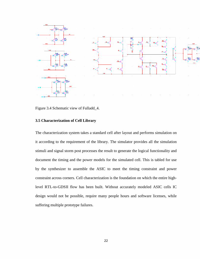
Figure 3.4 Schematic view of Fulladd_4.
3.5 Characterization of Cell Library
The characterization system takes a standard cell after layout and performs simulation on
it according to the requirement of the library. The simulator provides all the simulation
stimuli and signal storm post processes the result to generate the logical functionality and
document the timing and the power models for the simulated cell. This is tabled for use
by the synthesizer to assemble the ASIC to meet the timing constraint and power
constraint across corners. Cell characterization is the foundation on which the entire high-
level RTL-to-GDSII flow has been built. Without accurately modeled ASIC cells IC
design would not be possible, require many people hours and software licenses, while
suffering multiple prototype failures.

23
3.5.1 The Library Characterizer – SignalStorm
The main inputs in a library characterizer are a SPICE-format netlist that contains the
detailed of transistors in the cell, the setup file which have the all the information about
the condition of simulation and the transistor model files provided by foundry. The main
output of library characterization is a library database that contains timing and power
models for each of the cells. These models are then used in power and timing calculation.
The simulator used for characterization is called signal storm (see Figure 3.5)
Figure 3.5 Inputs and Outputs to SignalStorm Library Characterizer
SignalStorm performs the following steps for automatic cell library characterization [14]:
1. Analysis of Spice models of transistor circuits and recognition of the logic
structure and functionality.

24
2. Generation of the logic or function model for combinatorial, sequential and
tristate circuits.
3. Generation of electrical, logical and timing specification definitions for the circuit
such as pin directions and properties, pin to pin delays etc.
4. Generation of Delay Vectors.
5. Generation of Power Vectors.
6. Defining the cell library characterization environment by specifying parameters
such as the supply voltage, temperature, input slew rate, output load and process
corners (Fast ,Typical and Slow)
7. Execution of Spice netlist and summarizes the results see 8 below.
8. Generation of Abstract Library Format (ALF) file which can be further converted
to .LIB, .VHDL, .V and HTML files.
All cells need to characterized logically and electrically. Electrically the cells are
characterized for the propagation delays, input pin capacitances and current requirements.
Propagation delays are the tabulation of the intrinsic and load-dependent delays and
calculated for all pin-to-pin paths. Input pin capacitance consists of either the active
capacitance, which occurs when the output node switches or the passive capacitance
which occurs when the outputs remain in a stable state and wire parasitic. Current
consumption requirements are needed for power analysis. For sequential logic cells along
with the above data, the Signal Storm library characterizer characterizes the cell input
signal constraints, like setup time, hold time, release time, removal time, recovery time,
and minimum pulse width. Signal Storm characterizes sequential logic constraints by
using a delay-tolerance-based binary search method. The results are saved as a table of

25
input slew rates. Thus for the sequential logics Signal Storm library characterizer
generates the constraint definitions for the clock signal, data signal, preset signal and
clear signal[14]. Html format of output of Signalstorm is shown in appendix E.
3.5.2 Setup file
In the setup file all the condition required to accurately simulate our library are set, so
one need to be careful and accurate when developing inputs for the setup file. The
simulator will simulate with whatever input we give to it and the data may be of no use.
The old adage of garage in garbage applies 10 or more fold with the possibility of
garbage for every cell. One needs know about the functional detail of the parameters in
the setup file see appendix B 2.
a) Corner
Propagation delay depends on both the input slew rate and the output load capacitance.
Signal storm characterize the cells, in terms of different input slew rates and load
capacitance. To get the correct information about the timing and power model at different
conditions simulation is performed for three different corners that is “fast fast”, “typical
typical” and finally “slow slow” with the same input slew rate and load capacitance but
for different supply voltages, temperatures and processes as we see in Table 3.2 .For
example see section 1 of appendix C

26
Table3.2 Parameter used for different corners.
Corner Supply
Voltage
temperature process
Slow slow 3V 200˚C slow
Typical
typical
3.3V 27˚C typical
Fast fast 3.6V -25˚C fast
b) Voltage Threshold
In the setup file all the voltages are defined relatively see section 2 in appendix C. where
we can see the high level voltage “Vh” is 100% of the supply voltage and low level
voltage “Vl” is 0, the threshold voltage “Vth” is 50% of the supply and the high slew
voltage level “Vsh” is 90 % while low slew voltage level “Vsl” is 10% of the supply
voltage. Also the voltage threshold levels are same both for input rising/falling and output
rising/falling.
c) Intrinsic delay
This is a important parameter as it provides the frequency limit of the transistor. It is the
built in delay of the logic gates caused due to the frequency limit of the transistor. For
example in a NMOS as the electron move from the source to the drain it suffers collisions
and finally reach a saturation velocity as a result it takes a finite time to cross the length
of the transistor gate and cannot be any more faster. This finite time the electron takes is
the intrinsic delay of the NMOS transistor. While setting the values of input slew in the
set up file for characterization we have to take in to consideration the value of the

27
intrinsic delay to ensure selected slew times are NOT faster than intrinsic delay or 1/ωT.
This is merely wasting the run time of the tool at best and at worst documents slew times
faster than intrinsic delay than physically possible.
d) Input Slew
The input slew is the rate at which the input is rising / falling, the input slew with the
output load capacitance that the gate is driving dominates the delay of the gate. As
mentioned earlier the input slew cannot be lower than the intrinsic delay of the transistor
as the transistor cannot respond so fast and the upper limit of the input slew in the setup
file depends on maximum output slew that is acceptable.
e) Output Loading Capacitance CL
The capacitance seen by output pin of the cell determines the output slew. The load
capacitance should be selected as normalized load, for each gate drive strength from 1X
to 8X, i.e. 1X, 2X, 3X, 4X, 8X. When determining intrinsic delay in which case the
normalized load must be much smaller than the gate output capacitance i.e X/20 or lower.
Since the amount of delay and rise/fall times depends on both the input slew rate and the
capacitance seen by the output pin, the signal storm library characterizer executes
simulations by using different input slew rates and output loading capacitance
combinations and tabulating the results
f) Pin to Pin delay
The Signal Storm library characterizer provides the delay for specific cells called pin to
pin delay where pin-to-pin delay is the time that a change at an input pin takes to effect a
change at the output pin. The time is measured from the point when an input signal

28
switches through an input threshold voltage (Vthi) to the point when an output signal
switches through an output threshold voltage (Vtho), as shown in Figure 3.6. A detail
explanation of the Pin to Pin delay is given in appendix C.
Figure 3.6 Pin to pin Delays.
g) Setup time
The setup time is the time during which the input data to the input of the sequential logic
must remain stable prior to the arrival of the clock so that the correct value is latched at
the output.
h) Hold Time
It is defined as the minimum time that an input signal must remain stable after the active
clock signal to ensure that input value is correctly latched at the output.
It is evident in the example shown in fig 3.7.

29
Figure 3.7 Setup and Hold time constraints for a positive edge triggered flip-flop.
In signal storm the constraint on setup time and hold time is determined by delay-
tolerance-based binary search method that is the setup time should also be such that it
does not degrade the Clock-Q propagation time beyond a pre-determined tolerance value.
In Signal Storm library characterization, to ensure that set up time chosen is not so close
to the switching point that the simulation fails, it performs a delay tolerance check by
multiplying the delay from clock (CK) to the output Q by factor specified with
SG_BI_DRATIO variable. As soon as the CK-Q delay is more than delay tolerance
variable, the simulation is considered a failure and next iteration follows. The binary
search is defined in detail in appendix E and the parameters for binary search in the setup
file are in section 3 of appendix B 2

30
3.5.3 Output of the characterization
After characterizing the cells the input slew rate, output loading and calculated pin to pin
delay are saved as a two dimensional delay table. The output slew rate which is also
calculated by these Signal Storm SPICE simulations, is saved in a second table. There are
several types of standard formats in the industry for describing Cell Library’s
characterized data. Different tools from different vendors read the same information from
the technology libraries in their corresponding formats. Initially the output is in the alf
format which can be converted in to lib, html or verilog format.
Alf- Advanced Library Format is more descriptive than .lib format file. SignalStorm
generates this file as an output from its database. ALF can be further converted to .lib or
.html format using ‘alf2lib’ and ‘alf2html’ commands.
Lib – Synopsis Liberty Library is used by Synopsys products for synthesis, timing and
power information. This format supports most of the models; and is more or less the
industrial a standard.
3.6 Components of a cell library
Irrespective of the Cell library it must have all the information listed below to be used for
an ASIC design.
1. Circuit Schematics, Symbols, Layouts, Parasitic Extraction and
Abstracted views of each standard cell.
2. A model in Verilog /VHDL for all the cells.
3. File containing timing, power and logical functionality data for certain threshold
voltage, temperature, Process and operating voltage in a format that is accurate and
acceptable industry wide for synthesis and Place & Route (P&R).

31
4. Documentation of the cell library that contains the logical functionality of all cells
along with the timing and power data of the cells
5. Physical description of the cell in terms of information about the routing layer to
be used, the dimension of the cell and the information about the pins. This
physical description is needed by the automatic place and route tool and can be
obtained from the abstraction of the cell which is described in the next chapter.

32
CHAPTER 4
ABSTRACTION OF CELLS
4.1 Introduction
An abstract is a high-level representation of a layout view it contains information about
the type, size of the cell, position of pins or terminals, and the overall size of blockages.
The abstracts generated are based on physical layout, logical data, process technology
information, and specific cell-modeling requirements. Abstract views generated are used
in place of full layouts to improve the performance of place-and-route tools, such as
Cadence Encounter and Cadence Silicon Ensemble. After the place-and-route is
complete, the abstracts are replaced back with the layouts.
4.2 Launching the Abstract Generator
1. First we have to stream out the layout of the cells in .gds format, while streaming out
the cells we have to make sure that the pin information are not lost for which we have
to label all the pins with text information layer while drawing the layout. Steps of
streaming out are explained below.
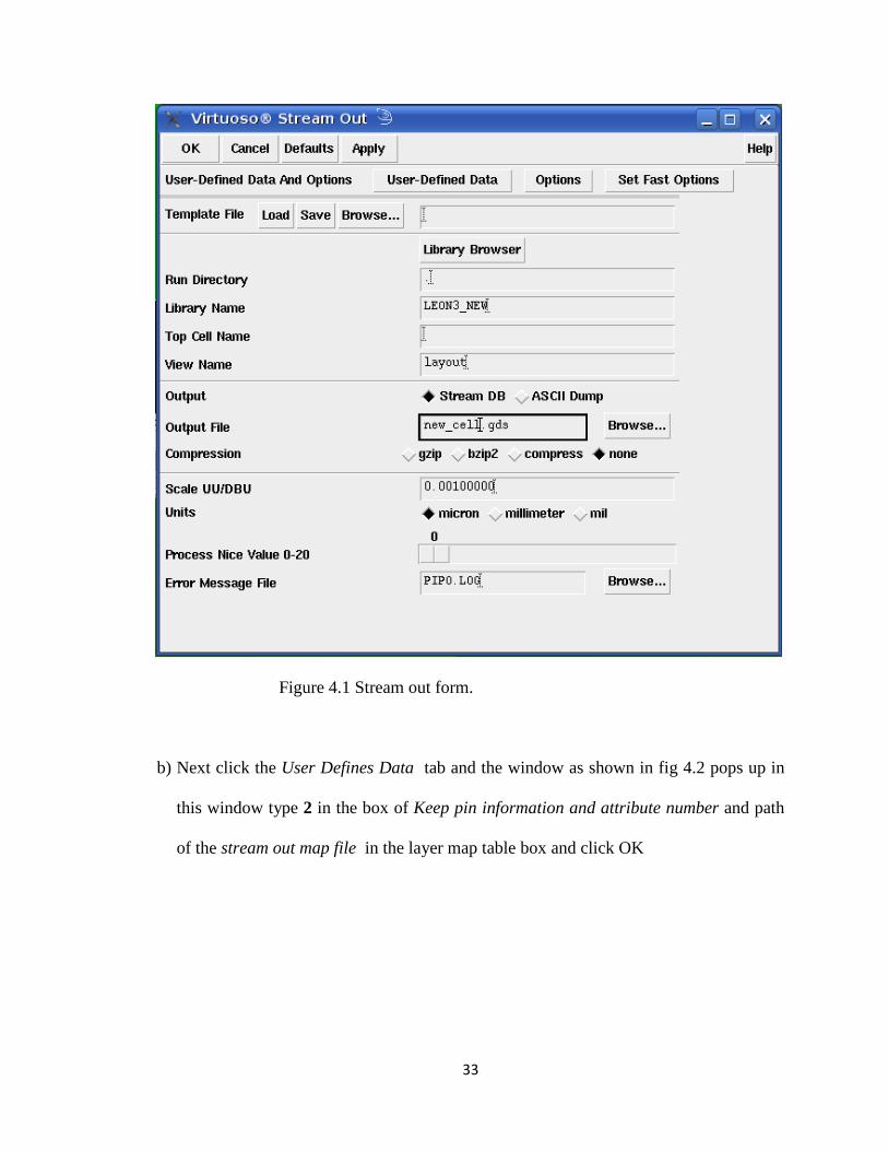
a)On the icfb window select File export stream. A window as shown in fig 4.1
pops up, where we have to type the name of the library such as LEON3_NEW in our
case and the name of gds file that will be generated which is new_cell.gds here.
33
Figure 4.1 Stream out form.
b) Next click the User Defines Data tab and the window as shown in fig 4.2 pops up in
this window type 2 in the box of Keep pin information and attribute number and path
of the stream out map file in the layer map table box and click OK

34
Figure 4.2 Stream out user defined data form.
c) In the next step click Option tab and the window as in Figure 4.3 pops up and the
window is filled up as shown in the diagram and click OK.
Then click OK on the window in Figure 4.1 and the streaming out starts and finally we
have to make sure that a error free completion result pops up.

35
Figure 4.3 Stream Out Option form.
2. The next step in Abstraction is to create a new library and attach the new library to the
proper technology file. We have to make sure that the technology file have all the
information needed for Abstraction(see section 4.3)
3. We launch the abstract generator from the open terminal by typing the command
abstract.
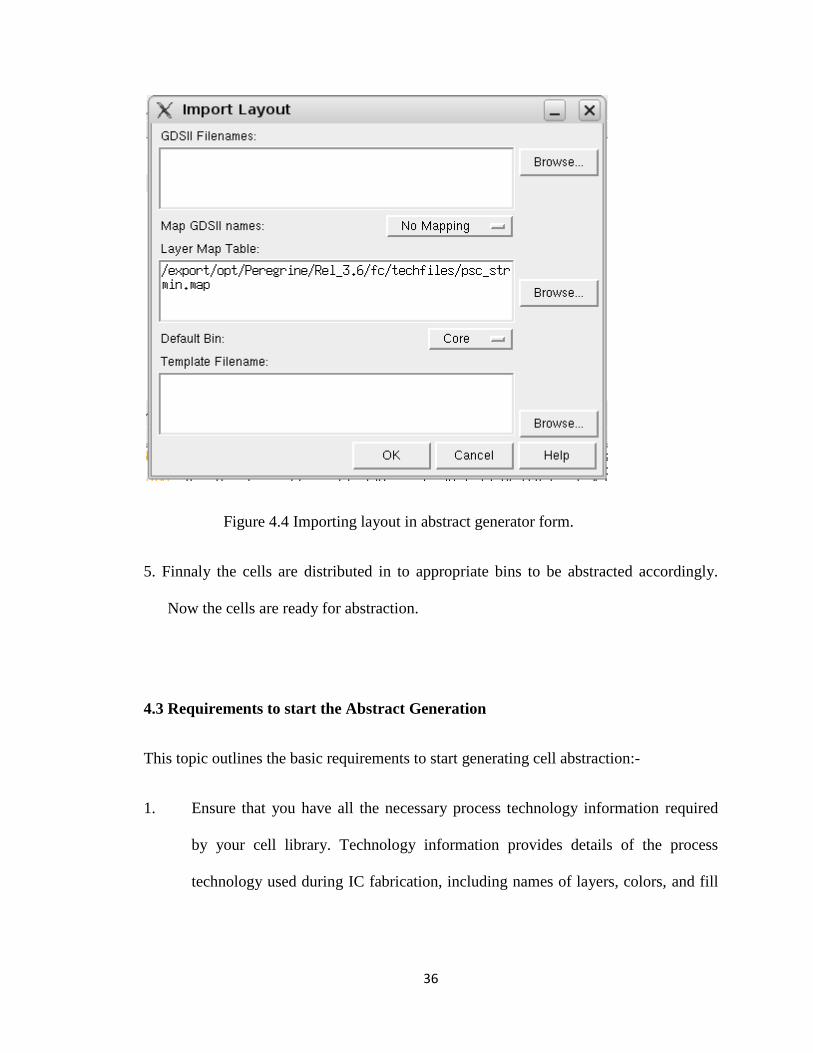
4. After the abstract terminal is opened we have to open the new library created and Click
File Import and the window swown in Figure 4.4 pops up where we have to enter
the gds file and the path of the stream in map file.
36
Figure 4.4 Importing layout in abstract generator form.
5. Finnaly the cells are distributed in to appropriate bins to be abstracted accordingly.
Now the cells are ready for abstraction.
4.3 Requirements to start the Abstract Generation
This topic outlines the basic requirements to start generating cell abstraction:-
1. Ensure that you have all the necessary process technology information required
by your cell library. Technology information provides details of the process
technology used during IC fabrication, including names of layers, colors, and fill

37
patterns, GDSII layer mapping data, and design rules for various layers and vias.
In our case the technology library is psc_PNR_FA_LEON3_08.
2. At times we may have the technology file in form of LEF file, in which case we
cannot directly attach the technology file to the library, first we have to convert it
into ASCII format and generate the technology file .
3. Provide the abstract generator with information about the physical (layout) or
logical construction of the cells in the library you want to process. You can do this
by importing various types of data, such as LEF, DEF, and GDSII. You can also
import logical information, typically represented in Verilog or Timing Library
Format (TLF), Compiled Timing Library Format (CTLF) and also Encrypted
Timing Library Format (ETLF).. In our case we have imported GDSII format file
of cells.
Figure 4.5 Types of Layout and Logical data that can be imported into the
abstract generator and the format of data that can be exported [17].

38
4.4 Create Abstracts
Whether you are generating abstracts for an entire library or for a few hierarchical blocks,
the approach is typically the same. You should initially focus on a small subset of cells or
blocks, establish option settings for this subset, and then process the remaining cells or
blocks in a single run.
1. Identify the cells with which you want to experiment, and begin to Generate
Abstracts for these cells.
2. Inspect the Results in the generated abstracts.
3. You can then begin to Modify Option Settings as required, and then rerun the
required steps.
4. If you are satisfied with the results, you can process the remaining cells in your
library.
5. After the abstraction is complete the abstracted information is export out in the
form of LEF file
4.5 Generate Abstracts
Each of the four main flow steps–Pins, Extract, Abstract, and Verify–have their own set
of options that control the way in which any cell is processed. You can make your initial
option settings either before you start generating abstracts or when you run any of the
individual steps.

39
4.5.1 Running Forms
Whenever you run any flow step, the abstract generator opens the Running step form.
This form allows you to modify only the options that are relevant to the steps you are
about to run. When you are satisfied with the options settings, generate the abstracts for
the selected cells. You can run the steps either one at a time or all at once for any or all of
the cells.
Four main steps of abstraction
a) Pins
The Running form for the Pin step is shown in Figure 4.2 has four tabs which are Map,
Text, Boundary and Blocks for the map tab we have to mention all the layer used for
labeling the pins, the name of the power pins and finally the name of the output pins as
all the pin are taken as input pin by default.
We leave the text tab form as it is, next for the boundary tab we have to choose always
instead of as needed and keep the block tab form blank and finally click run. Thus in the
Pins step, the abstract generator creates a place-and-route boundary for the cell and the
starting pin shapes for each of the nets to be extracted. It then matches the pins created
against those described in any logical view present and appends the appropriate pin
direction.

40
Figure 4.6 Running form for Pin step.

41
Figure 4.7 Running form for Extract step.
b) Extract
The Extract step running form is shown in Figure 4.7 also has four tabs which are Signal,
Power, Antenna, and General. In the Signal tab form we deselect extract signal nets but
for the power tab we have to select extract power net so that the whole power rails
geometries get converted into a pin geometry. The form for the antenna tab will be filled
automatically if the technology file contains all the required information for antenna
calculation, we only have to select how we want to calculate the antenna area. An

42
antenna rule generally calculates the metal side plus surface area to gate area ratio or the
metal surface area to gate area ratio by default. The last tab is the general in which we
have to mention the detail of the layers for metal1 to meta2 contact, metal2 to metal3
contact, poly to metal1 contact and finally active to metal1 contact.
Thus in the Extract step, the abstract generator derives which shapes are connected to
which nets by tracing the connectivity from the pin shapes created during the Pins step.
The tool also creates shape with purpose net in the top level of the extract view, and for
each such shape creates a pin on the appropriate net. The overlap boundary is also
calculated if required(when overlap boundary layer is present). Finally, the abstract
generator uses the antenna options to create library process antenna information for
custom blocks and standard cells. The resulting antenna model helps mitigate the
problem of gate damage caused during manufacturing.
c) Abstract
The abstract running form is shown in Figure 4.8 has six tabs in it Adjust, Blockage,
Fracture, Site, Overlap boundary and Grid. In the adjust tab we have to mention all
power pins and how they would be connected and oriented that is if they would be
abutted or feedthrough and facing the core or not . In the case of the core cells the power
rails are all abutted. In the blockage tab we have to choose “detailed” for all the metals,
the fracture tab form is kept as it is, for the Site form we have to type “CORE” as all the
cells in the library are of same height and are used for the core of leon3, the overlap
boundary switch is kept off and finally the grid for both metal1 and metal2 is chosen to
be 2.2 (Chapter 3) and offset is entered. For the LEON3 library offset is chosen to be 0.
Thus in the Abstract step, the abstract generator adjusts the pin shapes created during the

43
Extract step to create the final shapes required by place and route tools. It then fractures
these pin shapes into rectangles. Next, the abstract generator applies a layer blockage
model selected by the user to create the final blockage geometry in the abstract. The
blockage geometry is then optionally fractured into rectangles. It then removes from the
abstract all layers other than those with purpose pin, blockage or boundary
Figure 4.8 Running form for Abstract step.
and deletes the instance hierarchy. At this stage, all the required geometry is at the top
level of the abstract.

44
d) Verify
The verify running tab have two tabs which are terminal and Manufacturing grid
The Verify step in the abstract generation process involves a series of functionality
checks designed to detect any problems in the abstracts generated. During the Verify
step, terminals are compared for any differences that might exist between logical and
abstract views. Pin and geometry information on manufacturing grids is checked, and
each abstract is tested within the target place-and-route system.
4.6 Inspecting the result
Cell Pane: The first source of result evaluation comes from the Cell Pane in the main
window. The abstract generator uses color-coded symbols in the Cell pane to indicate the
result of a particular abstract generation flow step. A green/red signifying pass/fail
symbol attached to each cell in the cell matrix as observed in see Figure 4.9
corresponding to a particular step in the abstraction process steps.

45
Figure 4.9 Cell Pane showing various warning signs and progress in Abstraction Steps.
4.7 Layout Editor: - If you want to see a detailed graphical representation of any view,
you can use the Layout Editor. You can use the Layout Editor functions to examine the
pin and blockage geometry generated, the sizing and spacing applied, and to make minor
edits. To launch the Layout Editor, select Cells – Edit and select a view. See Figure 4.10

46
Figure 4.10 Abstract view of Cell and4_4.

47
CHAPTER 5
ANTENNA ERROR PROBLEM
5.1 Introduction
Antenna problems have existed in the chip manufacturing industry for more than one
decade. During wafer manufacturing, charge caused by UV light, etching etc accumulates
on the long floating wires. If the wire is connected to the input gate, the device may be
damaged. This reduces the wafer manufacturing yield. To prevent the damage we have to
find a way to bleed the accumulated charge. Analogies for antenna problems during
wafer manufacturing and normal operation are shown as Figures 5.1 and 5.2. During
manufacturing, the antenna diodes which are clamps connected to ground discharge the
accumulated charges on the long wires. The antenna diodes used in manufacturing are
such that do not load circuit function. They are reverse bias diodes and behave like an
open circuit with very little parallel capacitance added to input ports during normal
operation resulting in the transmitted signals maintaining their integrity. We get the data
of Antenna calculation of a cell in Extract step during abstraction.

48
Figure 5.1 Analogy of antenna problem during manufacturing [21].
Figure 5.2 Analogy of antenna problem during circuit normal operation[21].

49
5.2 Specific Requirements for Antenna Calculation
This section describes the technology file requirements for using the abstract generator
for antenna calculation. In Open Access 2.0, the metal layer thickness rule and also
default Antenna Rule for that metal layer need to be specified in the characterization rules
section which is a subclass of the electrical rules class in the technology file to perform
antenna calculation in the abstract generator. In the technology file on Open Access 2.2,
the antenna rules have been moved to the antenna Models section of the foundry
constraint group. You can specify a separate antenna Models group for each oxide type
and can specify antenna Models for up to four oxide types. The constraint specifies the
antenna ratios for one oxide type corresponding to a specific thickness of the gate oxide.
You can specify the thickness value in the tech Layer Properties subsection in the layer
Definitions section if a antenna side area calculation is to be performed.[17]
5.3 Antenna Ratio Definition
The total gate area that is electrically connected to a node (and therefore connected to the
process antennas) determines the amount of charge the electrically connected gates can
withstand, and because the size of the process antennas connected to the node determines
how much charge the antennas collect, it is useful to calculate the ratio of the size of the
process antennas on a node to the size of the gate area that is electrically connected to the
node. This ratio is called the antenna ratio of the corresponding metal. Greater the
antenna ratio, greater is the potential for damage to the gate oxide. If you check a chip
and obtain an antenna ratio greater than the threshold specified by the foundry, gate
damage is likely to occur.[17]

50
5.4 Antenna Rule Checking
Use layout verification tools to check antenna errors. The error reports should contain the
following information:[18]
1. The violated position of the wire: The (x,y) position of which the antenna ratio of
the wire exceeds the specified antenna ratio, e.g, 400 in our case .
2. Error flattened: Since the wire is connected to every module, it should not be
hierarchical. Therefore, the errors should be flattened. Set the error flattened
option if the tool is a hierarchical verification tool. If the verification tool is not
hierarchical, you do not need to set this option.
3. Chip level: At the chip level, since each block’s antenna problem is fixed, we only
need to consider the interconnection among the blocks. Since the whole chip may
be very large. If the chip is too big, chip-level antenna violations can be avoided
by putting a protection diode on every input pin. This can be done very quickly, in
general within few seconds to one minute. If the chip is not too big and run time is
acceptable, then antenna violation checking and dynamic diode dropping and
jumper insertion approaches can be used.
5.5 Solutions for Antenna Problem
The three solutions proposed to solve the antenna problem are described as follows: [19,
20]
1. Router options: Break signal wires and routes to upper levels. This reduces the
charge amount for each net during manufacturing. This is called the “jumper
approach.”

51
2. Embedded protection diode: Add protection diodes on every input port for
every standard cell. However these protection diodes consume the cell area
resources and increase manufacturing costs. Even though the diodes are not
necessary, these diodes are always embedded.
3. Dynamic dropping diode after placement and route: Fixing only the wire with
the antenna violation which will not waste routing resources. During wafer
manufacturing, all the inserted diodes are grounded. Since the input ports are high
impedance, the charge on the wire flows through the insert diode instead of
flowing into the device gate. One diode can be used to protect all input ports that
are connected to the same output
Table 5.1 Comparison of three Approaches [21].
From table 5.1 it can be observed that dynamic diode dropping has the following
advantages:
1. Least timing degradation (better than embedded) within the application
Impact Jumper Embedded diode
Dynamic diode dropping
Cell area No Yes No Routability/chip size
Yes Yes
No
Completeness No No Yes Timing Most More Least Integration Yes Yes No

52
2. Least waste of chip area.
3. Least impact on routability. The jumper only approach is unusable on very dense ICs
For the LEON3 Cell library dynamic diode dropping was used.
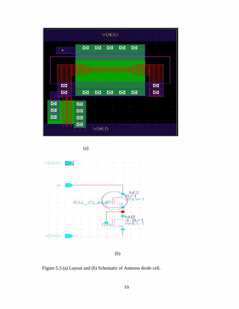
5.6 Description of the antenna diode used
Figure 5.3 shows the layout and the schematic of the antenna diode used. The RN Clamp
is the diode which actually serve the main purpose of bleeding the charge the diode
connected RN NMOS connected to it is there only to bypass the antenna error checking
because if the gate of the clamp is directly connected to the ground rails which are long
metal wires antenna error checking would generate antenna error for the antenna diode
itself.
53
(a)
(b)
Figure 5.3 (a) Layout and (b) Schematic of Antenna diode cell.

54
5.7 Procedures for Fixing Antenna Violations.
The procedure for fixing antenna violations are illustrated below
1 . We either drop the Antenna diode automatically as in encounter place and routing tool
have a option where you can specify the antenna diode cell and then the router
would automatically place and route the diode where ever its necessary.
2 . Another way is as follow.[21]
a. Bring up the tool for antenna fixing.
b. Create the new library or open the existing library.
c. Stream in GDSII file.
d. Import the Diode from the GDSII format or create them from scratch.
e. Open the top level cell.
f. Drop the diodes without extension wires according to the rule files specified.
g. Insert the jumper for the rest of the violation (if there is no space to drop a diode).
h. Increase the extension wire to accommodate a bigger area.
i. (Repeat Step .h until all the violations are cleaned.)
Save the design in a GDSII format.

55
CHAPTER 6
CONCLUSION
6.1 Conclusion
A 3.3V Digital standard Cell Library has been developed for LEON3 operable at 200°C
temperature. For the library we used the SOI process as it has some advantage over the
bulk. The dimension of IX NMOS is length 1µm and width 1.4µm and dimension of IX
PMOS is length 0.6µm and width 1.6µm. Some other important dimensions of the cells
like the height, the safety zone, the power rail width, the routing grid etc as given in table
3.1. In total we have 163 logical cells and 96 sequential cells. The cell have drive strength
of 1X to 4X the inverter and buffer have drive strength of up to 15X and 24X
respectively. The library has been characterized by using signal storm for timing and
power. After characterizing the cells they were abstracted for use in place and route. The
whole layout was validated by running DRC and LVS on the layout generated by the
place and route tool. Finally we were able to place and route the LEON3 within a area of
6.5mm by 6.5mm
6.2 Future Work
In the library we can have some more cells as we do not have all the combination of AO
(ANDOR) and AOI(ANDOR INVERTED). The antenna diode needs to be characterized

56
and also while doing place and route the antenna diode were not being dropped
automatically in some places where it is needed so we need to go through the place and
route tool to solve this problem.

57
REFERENCES
1. V.Madhuravasal, J.Wang, C.Hutchens, X.Zhu and Y.Zhang, "High Temperature
Silicon-on-Insulator (SOI) Deep Submicron Device Performance," HITEC 2006
Conference, Santa Fe, New Mexico, May 2006.
2. Development of a 5V digital cell library For Use With The Peregrine
Semiconductor Silicon on Sapphire (SOS) Process”, by Usha Badam,Thesis
,Oklahoma State University,2007.
3. Michael John and Sebastian Smith, “Application-Specific Integrated Circuits”,
Addison-Wesley Publishing Company, VLSI Design Series, June 1997.
4. P. F. Lu et al., “Floating-Body Effects in Partially Depleted SOI CMOS Circuits,”
in IEEE Journal of Solid-State Circuits, Vol. 32, No. 8, August 1997, pp. 1241-
1253.
5. P. McAdam and B.G. Goldberg, "CMOS SOS for Mixed Signal ICs," Peregrine
Semiconductor Corporation, June 2001.
6. SOI VS CMOS for Analog Circuit Vivian Ma, 961347420, University of Toronto
7. J.M. Stern, P. A. Ivey, S. Davidson, and S. N. Walker, “Silicon-On-Insulator
(SOI): A High Performance ASIC Technology,” (1992).

58
8. R. Howes, W.Redman-White, “A Small-Signal Model for the
Frequencydependent Drain Admittance in Floating Substrate MOSFETs”, IEEE J.
Sol. St. Ckts, 27( 8), Aug 1992.
9. C. T. Chuang, “Design Challenges for High-Performance SOI Digital CMOS
VLSI,” in International Symposium on VLSI Technology, Systems, and
Applications, 1999, pp. 270-273.
10. J.-P. Colinge, "Silicon-On-Insulator Technology: Materials to VLSI," 2 ed.:
Kluwer Academic Publishers, 2000
11. “Proposal for a 3.3V/5V Low Leakage High Temperature Digital Cell Library
Usign Stacked Transistors”, by Singaravelan Vishwanathan, Oklahoma State
University 2007.
12. “Characterizing a Cell Library Using ICCS”, Teri Hike McFaul Karl Perry, Intel
Corporation, ASIC Seminar and Exhibit, Sep 1990 Proceedings Third Annual
IEEE.
13. CMOS VLSI Design,A Circuits and Sytems Perspective”, by Neil .H.E.Weste and
David Harris ,Third Edition
14. SignalStorm Characterization Manual
15. Design of 5V digital standard cells and I/O libraries for military standard
temperature by Vibhore Jain, Thesis, Oklahoma State University, 2008.
16. “Automated Standard Cell Library Generation & study of Cell Library Functional
Content”, Yunbum Jung, University of Michigan
17. Abstract generator user guide

59
18. Peter H. Chen et al, “VLSI Design Flow,” National Semiconductor Corporation,
Santa Clara, CA 95052, May, 1997.
19. Michael Santarini, “Tool Automatically Removes Antenna Violations,” EE
Times, Issue 1013, p. 88, June 22, 1998.
20. Changsheng Ying, “Techniques for Removing Antenna Rule Violations,” Patent
Pending, Stanza System, Inc., Cupertino, California, 95014.
21. “Fixing antenna problem by dynamic diode dropping and jumper insertion” PH
Chen, S Malkani, CM Peng, J Lin - Proc. of ISQED, 2000
22. D. De Venutoa,*, M.J. Ohletzb “Floating body effects model for fault simulation
of fully depleted CMOS/SOI circuits”, Microelectronics Journal 34 (2003) 889–
895
23. Study of SOI Annular MOSFET by Swati Shah, Thesis, Oklahoma State
University, 2009.
.
60
APPENDIX A
Library Cells and Drive Strengths Specification
1. Drive Strengths
• For inverters : 1X, 2X, 3X, 4X, 6X, 8X,9X,12X,15X
• For buffer : 1X, 2X, 3X, 4X, 6X, 8X,9X, 11X,12X,14X,15X,18X,20X,22X, 24X
• Three State Buffers: 1X, 2X, 3X, 4X .
2. For others: Four drive strengths: 1X, 2X, 3X and 4X.
3. Core Cell List
Table 1: List of core cells
CELL TYPE
CELL NAME FUNCTION
Inverters Inv_X Y = not (A) Buffers buf_X Y = A NAND gates
nand2_X Y= not (A.B) nand3_X Y = not (A.B.C) nand4_X Y = not (A.B.C.D)
NOR gates nor2_X Y = not (A+B) nor3_X Y = not (A+B+C) nor4_X Y = not (A+B+C+D)

61
CELL TYPE
CELL NAME FUNCTION
AND gates nor2_X Y = not (A+B) nor3_X Y = not (A+B+C) nor4_X Y = not (A+B+C+D)
OR gates
and2_X Y = A.B and3_X Y = A.B.C and4_X Y = A.B.C.D
XOR gates xor_X Y = A⊕B XNOR gates xnor_X Y = not(A⊕B) AO gates ao21_X Y = (A0.A1)+B0
ao22_X Y = (A0.A1)+(B0.B1 ao32_X Y = (A0.A1.A2)+(B0.B1 ao33_X Y=(A0.A1.A2)+(B0.B1.B2) ao331_X Y=(A0.A1.A2)+(B0.B1.B2)+C0 ao322_X Y = A0.A1.A2)+(B0.B1)+(C0.C1) ao332_X Y = (A0.A1.A2)+(B0.B1.B2)+(C0.C1) ao333_X Y = (A0.A1.A2)+(B0.B1.B2)+(C0.C1.C2)
OA gates oa21_X Y = (A0+A1).B0 oa22_X Y = (A0+A1).(B0+B1) oa211_X Y = (A0+A1).B0.C0 oa221_X Y = (A0+A1).(B0+B1).C0 oa222_X Y = (A0+A1).(B0+B1).(C0+C1) oa31_X Y = (A0+A1+A2).B0 oa32_X Y = (A0+A1+A2).(B0+B1) oa33_X Y = (A0+A1+A2).(B0+B1+B2) oa311_X Y = (A0+A1+A2).B0.C0 oa321_X Y = (A0+A1+A2).(B0+B1).C0 oa331_X Y = (A0+A1+A2).(B0+B1+B2).C0 oa322_X Y = (A0+A1+A2).(B0+B1).(C0+C1) oa332_X Y = (A0+A1+A2).(B0+B1+B2).(C0+C1) oa333_X Y = (A0+A1+A2).(B0+B1+B2).(C0+C1+C2)
AOI gates aoi21_X Y = not((A0.A1)+B0) aoi22_X Y = not((A0.A1)+(B0.B1)) ao31_X Y = (A0.A1.A2)+B0 ao32_X Y = (A0.A1.A2)+(B0.B1 ao33_X Y = Y=(A0.A1.A2)+(B0.B1.B2) aoi331_X Y = not((A0.A1.A2)+(B0.B1.B2)+C0) aoi332_X Y = not((A0.A1.A2)+(B0.B1.B2)+(C0.C1)) aoi333_X Y =
not((A0.A1.A2)+(B0.B1.B2)+(C0.C1.C2))
CELL TYPE
CELL NAME FUNCTION
OAI gates oai21_X Y = not((A0+A1).B0)

62
oai22_X Y = not((A0+A1).(B0+B1)) oai211_X Y = not((A0+A1).B0.C0) oai221_X Y = not((A0+A1).(B0+B1).C0) oai222_X Y = not((A0+A1).(B0+B1).(C0+C1)) oai31_X Y = not((A0+A1+A2).B0) oai32_X Y = not((A0+A1+A2).(B0+B1)) oai33_X Y = not((A0+A1+A2).(B0+B1+B2)) oai311_X Y = not( (A0+A1+A2).B0.C0) oai321_X Y = not( (A0+A1+A2).(B0+B1).C0) oai331_X Y = not( (A0+A1+A2).(B0+B1+B2).C0) oai322_X Y = not( (A0+A1+A2).(B0+B1).(C0+C1)) oai332_X Y = not(
(A0+A1+A2).(B0+B1+B2).(C0+C1)) oai333_X Y = not(
(A0+A1+A2).(B0+B1+B2).(C0+C1+C2)) Multiplexers mux21_X Multiplexer 2 to 1
muxi21_X Multiplexer 2 to 1 with inverted output muxi41_X Multiplexer 4 to 1Multiplexers muxI41_X Multiplexer 4 to 1 with inverted output
Flip-Flops msdff_X D-type flip-flop with positive clock edge msdffnr_X D-type flip-flop with positive clock edge and
negative asynchronous reset msdffns_X D-type flip-flop with positive clock edge and
negative asynchronous set msdffnrns_X D-type flip-flop with positive clock edge and
negative asynchronous reset and set msdffn_X D-type flip-flop with negative clock edge msdffnnr_X D-type flip-flop with negative clock edge and
negative asynchronous reset msdffnns_X D-type flip-flop with negative clock edge and
negative asynchronous set msdffnnrns_X D-type flip-flop with negative clock edge and
negative asynchronous reset and set Three State Buffers
Tribuf_X Y = A.E; Y=HiZ for not E
Full adder Fulladd_X Full adder Half adder Halfadd_X Half adder Half subtractor
Halfsub_X Half subtractor

63
CELL TYPE
CELL NAME FUNCTION
Scan Flip-Flops
scanmsdff_X D-type flip-flop with positive clock edge with scan inputs
scanmsdffnr_X D-type flip-flop with positive clock edge and negative asynchronous reset with scan inputs
scanmsdffns_X D-type flip-flop with positive clock edge and negative asynchronous set with scan inputs
scanmsdffnrns_X
D-type flip-flop with positive clock edge and negative asynchronous reset and set with Scan inputs
scanmsdffn_X D-type flip-flop with negative clock edge with scan inputs
scanmsdffnnr_X
D-type flip-flop with negative clock edge and negative asynchronous reset with scan inputs
scanmsdffnns_X
D-type flip-flop with negative clock edge and negative asynchronous set with scan inputs Scan Flip-Flops
scanmsdffnrnns_X
D-type flip-flop with negative clock edge and negative asynchronous reset and set with scaninputs
Latches latch_X D-type transparent latch with positive clock level
latchnr_X D-type transparent latch with positive clock level and negative asynchronous reset
latchns_X D-type transparent latch with positive clock level and negative asynchronous set
latchnrns_X D-type transparent latch with positive clock level and negative asynchronous reset and set
latchn_X D-type transparent latch with negative clock level
latchnnr_X D-type transparent latch with negative clock level and negative asynchronous reset
latchnns_X D-type transparent latch with negative clock level and negative asynchronous set
latchnnrns_X D-type transparent latch with negative clock level and negative asynchronous reset and set

64
Table 2: Core cell count Cell Type Number of Logic Types Total Number of Cells Inverters 1 15 Buffers 1 16 3-State Buffers 1 4 Tie_high/low 2 2 NAND 3 12 NOR 3 12 AND 3 12 OR 3 12 XOR 1 4 XNOR 1 4 AO 7 28 OA 14 56

65
APPENDIX B Inputs to SignalStorm library Characterizer
1) A sample sub-circuit (netlist – inv_15a) file as an input to SignalStorm // Generated for: spectre // Generated on: Oct 3 12:28:59 2008 // Design library name: scratch // Design cell name: buf_inv // Design view name: schematic simulator lang=spectre global 0 include "/export/opt/Cadence/IC5141USR5/tools/dfII/samples/ artist/ahdlLib/quantity.spectre" // Library name: LEON3_NEW // Cell name: inv_15a // View name: schematic subckt inv_15a A VDDD VSSD Y M10 (net059 A VSSD) rnx w=2.8u l=1u mt=1 M8 (Y net18 VSSD) rnx w=7u l=1u mt=1 M4 (Y net18 VSSD) rnx w=7u l=1u mt=1 M6 (Y net18 VSSD) rnx w=7u l=1u mt=1 M0 (net18 net059 VSSD) rnx w=7u l=1u mt=1 M11 (net059 A VDDD) rp w=3.2u l=600n mt=1 M9 (Y net18 VDDD) rp w=8u l=600n mt=1 M5 (Y net18 VDDD) rp w=8u l=600n mt=1 M1 (net18 net059 VDDD) rp w=8u l=600n mt=1 M7 (Y net18 VDDD) rp w=8u l=600n mt=1 ends inv_15a // End of subcircuit definition.

66
2) A sample Setup file- for standard cells in typical process
[Process typical{ voltage = 5 ; temp = 27 ;
Corner = "tt" ;………………………………………………………………Section 1 Vtn = 0.755 ;
Vtp = 0.654 ; ] };
[Signal std_cell { unit = REL; Vh=1.0 1.0; Vl=0.0 0.0; Vth=0.5 0.5;
Vsh=0.9 0.9;………………………………………………………………………Section 2 Vsl=0.1 0.1;
tsmax=10.0n; ] };
[Simulation std_cell{ transient = 0.1n 50n 50p; dc = 0.26 5 0.03;
bisec = 12.0n 12.0n 150p;……………………………….Section3 resistance = 10MEG; ] }; Index X1{ Slew = 1n 2n 4n 6n 8n; Load = 0.0005p 0.009p 0.017p 0.034p 0.068p 0.136p; }; Index X2{ Slew = 1n 2n 4n 6n 8n; Load = 0.0005p 0.017p 0.034p 0.068p 0.136p 0.272p; }; Index X3{

67
Slew = 1n 2n 4n 6n 8n; Load = 0.0005p 0.026p 0.052p 0.104p 0.208p 0.416p; }; Index X4{ Slew = 1n 2n 4n 6n 8n; Load = 0.0005p 0.034p 0.068p 0.136p 0.272p 0.544p; }; Index X5{ Slew = 1n 2n 4n 6n 8n; Load = 0.0005p 0.043p 0.086p 0.172p 0.344p 0.688p; }; Index X6{ Slew = 1n 2n 4n 6n 8n; Load = 0.0005p 0.052p 0.104p 0.208p 0.416p 0.832p; }; Index X7{ Slew = 1n 2n 4n 6n 8n; Load = 0.0005p 0.06p 0.12p 0.24p 0.48p 0.96p; }; Index X8{ Slew = 1n 2n 4n 6n 8n; Load = 0.0005p 0.068p 0.136p 0.272p 0.544p 1.088p; }; Index X9{ Slew = 1n 2n 4n 6n 8n; Load = 0.0005p 0.077p 0.154p 0.308p 0.616p 1.232p; }; Index X10{ Slew = 1n 2n 4n 6n 8n; Load = 0.0005p 0.086p 0.172p 0.344p 0.688p 1.372p; }; Index X11{ Slew = 1n 2n 4n 6n 8n; Load = 0.0005p 0.095p 0.19p 0.38p 0.76p 1.52p; }; Index X12{ Slew = 1n 2n 4n 6n 8n;

68
Load = 0.0005p 0.103p 0.206p 0.412p 0.824p 1.648p; }; Index X14{ Slew = 1n 2n 4n 6n 8n; Load = 0.0005p 0.12p 0.24p 0.48p 0.96p 1.92p; }; Index X15{ Slew = 1n 2n 4n 6n 8n; Load = 0.0005p 0.129p 0.258p 0.516p 1.032p 2.064p; }; Index X18{ Slew = 1n 2n 4n 6n 8n; Load = 0.0005p 0.155p 0.310p 0.620p 1.240p 1.48p; }; Index X20{ Slew = 1n 2n 4n 6n 8n; Load = 0.0005p 0.172p 0.344p 0.688p 1.372p 2.744p; }; Index X22{ Slew = 1n 2n 4n 6n 8n; Load = 0.0005p 0.19p 0.38p 0.76p 1.52p 2.323p; }; Index X24{ Slew = 1n 2n 4n 6n 8n; Load = 0.0005p 0.206p 0.412p 0.824p 1.648p 3.292p; }; Index Clk_Slew{ bslew = 0.5n 2n 10.0n; }; Group X1{ CELL = *1; }; Group X2{ CELL = *2; }; Group X3{ CELL = *3; }; Group X4{ CELL = *4; }; Group X5{ CELL = *5; };

69
Group X6{ CELL = *6; }; Group X7{ CELL = *7; }; Group X8{ CELL = *8; }; Group X9{ CELL = *9; }; Group X10{ CELL = *10; }; Group X11{ CELL = *11; }; Group X12{ CELL = *12; }; Group X14{ CELL = *14; }; Group X15{ CELL = *15; }; Group X18{ CELL = *18; }; Group X20{ CELL = *20; }; Group X22{ CELL = *22; }; Group X24{ CELL = *24; };

70
Group X1a{ CELL = *1a; }; Group X5a{ CELL = *5a; }; Group Clk_Slew{ PIN = *.CLK ; }; Margin m0 { setup = 1.0 0.0 ; hold = 1.0 0.0 ; release = 1.0 0.0 ; removal = 1.0 0.0 ; recovery = 1.0 0.0 ; width = 1.0 0.0 ; delay = 1.0 0.0 ; power = 1.0 0.0 ; cap = 1.0 0.0 ; } ; Nominal n0 { delay = 0.5 0.5 ; power = 0.5 0.5 ; cap = 0.5 0.5 ; } ; set process(typical){ simulation = std_cell; signal = std_cell; margin = m0; nominal = n0; }; set index(typical){ Group(X1) = X1; Group(X2) = X2; Group(X3) = X3; Group(X4) = X4; Group(X5) = X5; Group(X6) = X6; Group(X7) = X7; Group(X8) = X8; Group(X9) = X9; Group(X10) = X10; Group(X11) = X11; Group(X12) = X12; Group(X14) = X14; Group(X15) = X15; Group(X18) = X18;

71
Group(X20) = X20; Group(X22) = X22; Group(X24) = X24; Group(X1a) = X1; Group(X5a) = X5; Group(Clk_Slew) = Clk_Slew; };
3) A sample batch file, which is used to specify the commands
and set values to SignalStorm-
#Specify the environment variable setting. EC_SIM_USE_LSF=1; EC_SIM_LSF_CMD=" "; EC_SIM_LSF_PARALLEL=10; EC_SIM_TYPE="spectre"; EC_SIM_NAME= "spectre"; EC_SPICE_SIMPLIFY=1; EC_CHAR="ECSM-TIMING ECSM-POWER"; #Specify the characterization input. SUBCKT="inv_buf_1.scs"; MODEL="model_tt.scs"; DESIGNS="buf_1 buf_11 buf_12 buf_14 buf_15 buf_18 b uf_2 buf_20 buf_22 buf_24 buf_3 buf_4 buf_5 buf_6 buf_8 buf_9 i nv_1 inv_12 inv_12a inv_15 inv_15a inv_2 inv_3 inv_4 inv_5 inv_ 6 inv_6a inv_8 inv_8a inv_9 inv_9a"; SETUP="setup_typical_new.ss"; PROCESS="typical";

72
APPENDIX C
Delay components
There are a number of delay models with a tradeoff between accuracy and performance
as the accuracy of the synthesized circuit depends upon the level of details and accuracy
with which the individual cells have been characterized. One of the popular delay models
is illustrated in Figure 3.6 and is briefly described here. The total delay of a
combinational logic gate, TDTOTAL has four components which are represented by the
following equation:
Figure 3.6 Delay components of a combinational logic gate [15]
Total Delay =Edge Delay + Intrinsic Delay + Transition Delay+ Interconnect Delay

73
The first term Edge delay is delay due to the input slew rate that is rate of input rise/fall
the second is the intrinsic delay which is the delay to drive a cell’s own internal
capacitance. The third term transition-output rise/fall) is the transition delay which is due
to the output load capacitance CL. The last term is interconnect delay or the wire delay it
is the time taken by a waveform to travel along the wire connecting driving output pin to
the input pin.
As mentioned before the library is characterized to determine the propagation delay that
is the delay from each input pin to the output pin and the output transition time. These
values are usually measured between pre-determined threshold values of the signal edges.
The of measuring these two delay values is illustrated in Figure 3.6. In simple term the
total delay consist intrinsic delays transition delays where transition delay are affected by
the input transition and loading of the gate and by the wire delay.
voltage
Time
Propagation delay
Output
transition
time
Input
transition
time
Figure 3.7 Measurements of propagation time and output transition time [16]

74
The threshold value for measurement of the propagation time is red from 50% of the
input voltage to 50% of output voltage signal. The output transition time and the input
transition time is measured from either 10% – 90% of the voltage for rising signal or 90%
- 10% for a falling signal. The values of output transition time and propagation time are
required for gate level synthesis and delay calculation tools.

75
APPENDIX D
Binary search[15]
Start - The value assigned to this parameter should be a simulation point of Data
transition lead with respect to active clock edge for which setup timing constraint is
guaranteed to meet. You can be liberal in choosing this value except that it might take bit
more of a time for convergence. You should perform simulations before you know that
what you are providing is a pass point. It is not worthy to spend much time on this since
if you can pick some value and start running simulation, SignalStorm should issue an
error message saying that the timing is not converging.
End - The value assigned to this parameter should be a simulation point of data
transition lag with respect to active clock edge for which setup timing is guaranteed to
fail. The explanation under "start" parameter holds well for this "end" parameter.
Resolution - The maximum value of error in setup/hold time that is tolerable for you
library. Resolution should be a value less than the delay of fastest gate in your cell
library.
Binary search is done to locate the output variable target value within a search
range of the input variable by iteratively halving that range to converge rapidly on the
target value. The measured value of the output variable is compared with the target value
for each iteration. In a binary search for setup time, the initial latest Pass Point equals

76
Start, and the initial latest Fail Point equals end. In a binary search for hold time, the
initial latest Pass Point equals end, and the initial latest Fail Point equals -Start. If the
simulation result for the output Q is the same as the expected waveform (rise or fall), and
the CK to Q delay satisfies the delay tolerance check, the simulation passes. Otherwise,
the simulation fails.
Figure 3.9 Setup time measurements using binary search [16]
As seen in the above Figure the lower bound of data transition that is point 1 is early
enough so the out is correct and the upper bound of data transition that is point 2 is
enough late so that the output would not latch up correctly. Hence the setup time
constraint lies between the upper and lower bounds. The binary search algorithm test the
data at the midpoint, point 3 between the lower bound point 1 and the upper bound point
2 as in the above case the as point 3 dose not pass the delay tolerance delay so now point

77
3 is the new upper bound but if point 3 would pass the delay tolerance test then the point
3 would have been the new lower bound. Then the algorithm tests data transition at the
new midpoint within the new range again. In this way the binary search algorithm,
iterates by setting a new boundary and a midpoint until the binary search reaches the
correct value of setup time. The data transition 4 is found to be the latest point that
satisfies the setup time constraint with an acceptable Clock-to-Q delay. Hold time
measurement is identical to setup time which follows the iterative binary search
technique.

78
APPENDIX E
HTML Format Data From Characterization
and2_2 (value: delay=typ, power=typ, check=typ, cap=typ)
Function Y=(A&B)
Static Power:
When Static Power [nW] - -0.399061
Port:
Name Direction
A INPUT
B INPUT
Y OUTPUT
Name Pin Capacitance [pF] Internal Power [pJ]
Rise Fall Rise Fall
A 0.0139333 0.0138776 0.041643 0.043777
B 0.00972403 0.0099866 0.040038 0.052374
Output Driving Strength
Name Rise Fall
Strength (sec/F) Limit (pF) Strength (sec/F) Limit (pF)
Y 3166.64 0.90334 3517.06 0.90334

79
Link To Path
PATH WHEN
(01A=>01Y) -
(10A=>10Y) -
(01B=>01Y) -
(10B=>10Y) -
(01A=>01Y)
DELAY [ns]
cl[pF] 0.0005 0.017 0.034 0.068 0.136 0.272
ts[ns] 0.8 0.34779 0.445756 0.516854 0.640455 0.863096 1.29319 1.6 0.385074 0.49005 0.567611 0.690138 0.917296 1.34577 3.2 0.402119 0.517363 0.608256 0.732593 0.966903 1.40776 4.8 0.407276 0.52938 0.616459 0.770297 1.01438 1.46503 6.4 0.390878 0.517181 0.61473 0.764712 1.0188 1.47911
POWER [ns]
cl[pF] 0.0005 0.017 0.034 0.068 0.136 0.272
ts[ns] 0.8 0.155699 0.139963 0.13723 0.137413 0.138103 0.139864 1.6 0.2253 0.203213 0.196918 0.190701 0.187678 0.188107 3.2 0.406732 0.372323 0.351347 0.344783 0.332412 0.322209 4.8 0.566657 0.532522 0.512367 0.495018 0.474498 0.462633 6.4 0.738222 0.697384 0.674808 0.647735 0.6266 0.60817
(01B=>01Y)
DELAY [ns]
cl[pF] 0.0005 0.017 0.034 0.068 0.136 0.272
ts[ns] 0.8 0.351366 0.446903 0.518764 0.641994 0.8634 1.29463
80
1.6 0.425195 0.522118 0.593029 0.717374 0.940905 1.38117 3.2 0.519516 0.625139 0.701874 0.828328 1.05934 1.49502 4.8 0.57806 0.686695 0.762127 0.895965 1.12548 1.57839 6.4 0.625458 0.743452 0.827435 0.962781 1.19853 1.65194
POWER [ns]
cl[pF] 0.0005 0.017 0.034 0.068 0.136 0.272
ts[ns] 0.8 0.176852 0.155548 0.150794 0.147982 0.14658 0.146466 1.6 0.242399 0.220696 0.212362 0.203901 0.201439 0.197298 3.2 0.393551 0.360894 0.347364 0.335583 0.326597 0.319554 4.8 0.556272 0.526036 0.509347 0.489233 0.468561 0.45589 6.4 0.703562 0.660795 0.638347 0.614843 0.596843 0.58262
(10B=>10Y)
DELAY [ns]
cl[pF] 0.0005 0.017 0.034 0.068 0.136 0.272
ts[ns] 0.8 0.385573 0.482232 0.554255 0.683367 0.92503 1.40115 1.6 0.4878 0.596218 0.672629 0.802211 1.03656 1.51886 3.2 0.625927 0.754935 0.841011 0.982552 1.23005 1.70236 4.8 0.764088 0.852312 0.965914 1.1302 1.41499 1.86165 6.4 0.854047 0.978841 1.08012 1.2517 1.53779 2.01867
POWER [ns]
cl[pF] 0.0005 0.017 0.034 0.068 0.136 0.272
ts[ns] 0.8 0.306591 0.288236 0.286669 0.28754 0.289528 0.291356 1.6 0.398971 0.372835 0.366015 0.358319 0.353059 0.3443 3.2 0.539715 0.502931 0.491236 0.481563 0.474932 0.471261 4.8 0.703652 0.646135 0.628885 0.617917 0.610012 0.595828 6.4 0.847904 0.792015 0.769811 0.756383 0.742184 0.728419

81
scanmsdff_1 (value: delay=typ, power=typ, check=typ, cap=typ)
Function FLIPFLOP{ DATA=(SEN?(SData:Data)) CLOCK=CLK Q=net0159 QN=net0155
} Q=net0159 Qb=net0155
Static Power:
When Static Power [nW] - -2.42003
Port:
Pin Direction Signaltype Polarity
CLK INPUT CLOCK RISING_EDGE
Data INPUT DATA -
Q OUTPUT - -
Qb OUTPUT - -
SData INPUT DATA -
SEN INPUT DATA -
Name Pin Capacitance [pF] Internal Power [pJ]
Rise Fall Rise Fall
CLK 0.00971528 0.00970863 0.171386 0.433195
Data 0.0133549 0.0136452 0.20888 0.332437
SData 0.017516 0.017494 0.257314 0.396884
SEN 0.00971025 0.00970859 0.464644 0.643153
Output Driving Strength

82
Name Rise Fall
Strength (sec/F) Limit (pF) Strength (sec/F) Limit (pF)
Q 6499.18 0.416884 8020.12 0.416884
Qb 10265.8 0.405155 11712.6 0.405155
Link To Path
PATH WHEN
(01CLK=>01Q) -
(01CLK=>10Q) -
(01CLK=>01Qb) -
(01CLK=>10Qb) -
Link To Constraint
Type Path
SETUP (01SEN=>01CLK)
SETUP (10SEN=>01CLK)
HOLD (01CLK=>01SEN)
HOLD (01CLK=>10SEN)
SETUP (01SData=>01CLK)
SETUP (10SData=>01CLK)
HOLD (01CLK=>01SData)
HOLD (01CLK=>10SData)
SETUP (01Data=>01CLK)
SETUP (10Data=>01CLK)
HOLD (01CLK=>01Data)
HOLD (01CLK=>10Data)
PULSEWIDTH (01CLK=>10CLK)
PULSEWIDTH (10CLK=>01CLK)
(01CLK=>01Q)
DELAY [ns]
cl[pF] 0.0005 0.009 0.017 0.034 0.068 0.136
ts[ns] 0.08 0.813984 0.903224 0.979779 1.124 1.36817 1.81013 0.32 0.863942 0.953551 1.02999 1.17422 1.41789 1.85362 0.64 0.933416 1.02225 1.09842 1.24288 1.48626 1.92674 1.2 1.04554 1.13389 1.2102 1.35503 1.59782 2.03565

83
1.6 1.11426 1.20368 1.28084 1.42517 1.66832 2.11009 2.4 1.22162 1.31058 1.38766 1.53182 1.77698 2.21434
POWER [ns]
cl[pF] 0.0005 0.009 0.017 0.034 0.068 0.136
ts[ns] 0.08 0.280533 0.277862 0.277531 0.278067 0.280238 0.286194 0.32 0.28039 0.277827 0.277558 0.277962 0.279973 0.28533 0.64 0.286615 0.283968 0.283638 0.284121 0.286159 0.29185 1.2 0.303506 0.300515 0.300274 0.300766 0.302599 0.307813 1.6 0.315098 0.312685 0.31251 0.313181 0.315141 0.321158 2.4 0.342174 0.338996 0.338829 0.339912 0.3414 0.346799
(01CLK=>10Q)
DELAY [ns]
cl[pF] 0.0005 0.009 0.017 0.034 0.068 0.136
ts[ns] 0.08 0.865242 0.960502 1.04869 1.21501 1.50548 2.05083 0.32 0.912297 1.01023 1.09869 1.265 1.55615 2.09947 0.64 0.983748 1.08129 1.16951 1.33584 1.62716 2.17205 1.2 1.11033 1.20695 1.29509 1.46108 1.75147 2.29473 1.6 1.18017 1.27665 1.36423 1.53007 1.82065 2.36551 2.4 1.34665 1.44124 1.52686 1.69053 1.97938 2.52355
POWER [ns]
cl[pF] 0.0005 0.009 0.017 0.034 0.068 0.136
ts[ns] 0.08 0.258511 0.257227 0.257392 0.259312 0.263316 0.271672 0.32 0.257292 0.255625 0.256089 0.257785 0.261707 0.270199 0.64 0.261879 0.260341 0.261078 0.262878 0.266819 0.275344 1.2 0.276012 0.274096 0.274765 0.276381 0.280558 0.289171 1.6 0.30137 0.2996 0.300042 0.301584 0.305374 0.31401 2.4 0.333431 0.330367 0.330415 0.331031 0.33392 0.341472
(01CLK=>01Qb)
DELAY [ns]

84
cl[pF] 0.0005 0.009 0.017 0.034 0.068 0.136
ts[ns] 0.08 0.926727 1.13136 1.30259 1.64263 2.27375 3.51034 0.32 0.975882 1.18122 1.35382 1.68964 2.3278 3.55942 0.64 1.04607 1.2519 1.42654 1.76339 2.39463 3.61958 1.2 1.17237 1.37809 1.5507 1.88643 2.51888 3.75256 1.6 1.24221 1.44732 1.62218 1.95663 2.58749 3.82507 2.4 1.40874 1.61099 1.78407 2.11582 2.7454 3.97144
POWER [ns]
cl[pF] 0.0005 0.009 0.017 0.034 0.068 0.136
ts[ns] 0.08 0.258511 0.257227 0.257392 0.259312 0.263316 0.271672 0.32 0.257292 0.255625 0.256089 0.257785 0.261707 0.270199 0.64 0.261879 0.260341 0.261078 0.262878 0.266819 0.275344 1.2 0.276012 0.274096 0.274765 0.276381 0.280558 0.289171 1.6 0.30137 0.2996 0.300042 0.301584 0.305374 0.31401 2.4 0.333431 0.330367 0.330415 0.331031 0.33392 0.341472
(01CLK=>10Qb)
DELAY [ns]
cl[pF] 0.0005 0.009 0.017 0.034 0.068 0.136
ts[ns] 0.08 0.903726 1.11393 1.29023 1.63482 2.28436 3.54994 0.32 0.951664 1.16318 1.3411 1.68623 2.33144 3.58528 0.64 1.02062 1.23393 1.40982 1.75615 2.40197 3.65709 1.2 1.13165 1.34506 1.52167 1.86856 2.50881 3.75463 1.6 1.20118 1.41422 1.59271 1.93984 2.58494 3.83915 2.4 1.30794 1.5195 1.69582 2.0456 2.69756 3.9467
POWER [ns]
cl[pF] 0.0005 0.009 0.017 0.034 0.068 0.136
ts[ns] 0.08 0.280533 0.277862 0.277531 0.278067 0.280238 0.286194 0.32 0.28039 0.277827 0.277558 0.277962 0.279973 0.28533 0.64 0.286615 0.283968 0.283638 0.284121 0.286159 0.29185 1.2 0.303506 0.300515 0.300274 0.300766 0.302599 0.307813 1.6 0.315098 0.312685 0.31251 0.313181 0.315141 0.321158

85
2.4 0.342174 0.338996 0.338829 0.339912 0.3414 0.346799
Timing Constraints
SETUP(01SEN=>01CLK)
re [ns] 0.4 1.6 8
co [ns] 0.8 1.3437 1.3437 1.0312 1.6 1.5 1.5 1.2812 3.2 1.71875 1.71875 1.5937 4.8 1.9375 1.9375 1.7187 6.4 2.0625 2.0625 2.0312
Timing Constraints
SETUP(10SEN=>01CLK)
re [ns] 0.4 1.6 8
co [ns] 0.8 0.9687 0.875001 0.6563 1.6 1.125 1.0312 0.7187 3.2 1.25 1.15625 1.0312 4.8 1.28125 1.1875 1.0625 6.4 1.3125 1.3125 1.0937
Timing Constraints
HOLD(01CLK=>01SEN)
re [ns] 0.4 1.6 8
co [ns] 0.8 -0.5938 -0.4063 0.374999 1.6 -0.75 -0.5625 0.21875 3.2 -1.0625 -0.7813 -0.093749 4.8 -1.1875 -1 -0.2188 6.4 -1.4063 -1.125 -0.4375
86
Timing Constraints
HOLD(01CLK=>10SEN)
re [ns] 0.4 1.6 8
co [ns] 0.8 -0.3125 -0.0313 0.75 1.6 -0.375 -0.093801 0.59375 3.2 -0.5 -0.2188 0.46875 4.8 -0.5313 -0.3438 0.4375 6.4 -0.5625 -0.375 0.406199
Timing Constraints
SETUP(01SData=>01CLK)
re [ns] 0.4 1.6 8
co [ns] 0.8 0.7812 0.7812 0.468699 1.6 0.9375 0.9375 0.7187 3.2 1.0625 1.0625 0.8437 4.8 1.1875 1.28125 0.968701 6.4 1.3125 1.40625 1.1875
Timing Constraints
SETUP(10SData=>01CLK)
re [ns] 0.4 1.6 8
co [ns] 0.8 0.5 0.4062 0.0937 1.6 0.5625 0.4687 0.1563 3.2 0.6875 0.5937 0.1875 4.8 0.71875 0.625 0.2187 6.4 0.750001 0.656251 0.25

87
Timing Constraints
HOLD(01CLK=>01SData)
re [ns] 0.4 1.6 8
co [ns] 0.8 -0.125 0.156199 0.843749 1.6 -0.1875 0.0937 0.874999 3.2 -0.3125 -0.0313 0.75 4.8 -0.3438 -0.1563 0.625 6.4 -0.4688 -0.1875 0.5
Timing Constraints
Timing Constraints
HOLD(01CLK=>01Data)
re [ns] 0.4 1.6 8
co [ns] 0.8 -0.0313 0.25 0.9375 1.6 -0.0938 0.0937 0.874999 3.2 -0.2188 -0.0313 0.75 4.8 -0.3438 -0.1563 0.53125 6.4 -0.4688 -0.2813 0.5
Timing Constraints
HOLD(01CLK=>10Data)
re [ns] 0.4 1.6 8
co [ns] 0.8 -0.3125 -0.2188 0.09375 1.6 -0.2813 -0.2813 0.031249 3.2 -0.3125 -0.3125 -1e-06 4.8 -0.3438 -0.25 0.062499 6.4 -0.375 -0.2813 0.0312
Timing Constraints
88
PULSEWIDTH(01CLK=>10CLK)
ts [ns] 0.08 0.32 0.64 1.2 1.6 2.4 0.926727 0.975882 1.04607 1.17237 1.24221 1.40874
Timing Constraints
PULSEWIDTH(10CLK=>01CLK)
ts [ns] 0.08 0.32 0.64 1.2 1.6 2.4 0.789206 0.836789 0.901693 0.970503 1.02119 1.07746

89
APPENDIX F
Example of LEF File
#****** # Preview export LEF # # Preview sub-version 5.10.41_USR5.90.69 # # REF LIBS: LEON3_NEW # TECH LIB NAME: psc_PNR_FA_LEON3_08 # TECH FILE NAME: techfile.cds #****** VERSION 5.5 ; NAMESCASESENSITIVE ON ; DIVIDERCHAR "/" ; BUSBITCHARS "[]" ; UNITS DATABASE MICRONS 100 ; END UNITS MANUFACTURINGGRID 0.050000 ; LAYER plocos TYPE MASTERSLICE ; END plocos LAYER nlocos TYPE MASTERSLICE ; END nlocos LAYER poly TYPE MASTERSLICE ; END poly LAYER contact TYPE CUT ; SPACING 0.80 ;

90
END contact LAYER metal1 TYPE ROUTING ; WIDTH 1.20 ; # mim m1 width to single via width? SPACING 0.80 ; SPACING 2.2 RANGE 10 60 ; # OFFSET 1.20 ; Defalut is 1/2 PITCH PITCH 2.20 ; # isolated via to via spacing via plus overlap plus m to m spacing DIRECTION HORIZONTAL ; CAPACITANCE CPERSQDIST 0.0000690000 ; RESISTANCE RPERSQ 0.04800000 ; EDGECAPACITANCE 0.000053000000 ; HEIGHT 1.17000000 ; THICKNESS 0.85000000 ; WIREEXTENSION 0.45000000 ; ANTENNAMODEL OXIDE1 ; ANTENNASIDEAREARATIO 200.00 ; END metal1 LAYER via TYPE CUT ; SPACING 1.00 ; ANTENNAMODEL OXIDE1 ; # via to via spacing END via LAYER metal2 TYPE ROUTING ; WIDTH 1.20 ; # mim m2 width to single via width? SPACING 0.80 ; SPACING 2.2 RANGE 10 60 ; # OFFSET 1.20 ; Defalut is 1/2 PITCH PITCH 2.20 ; # isolated via to via spacing via plus overlap plus m to m spacing DIRECTION VERTICAL ; CAPACITANCE CPERSQDIST 0.0000180000 ; RESISTANCE RPERSQ 0.03200000 ; EDGECAPACITANCE 0.000042000000 ; HEIGHT 3.42000000 ; THICKNESS 0.98000000 ; WIREEXTENSION 0.45000000 ; ANTENNAMODEL OXIDE1 ; ANTENNASIDEAREARATIO 200.00 ; END metal2 LAYER via2 TYPE CUT ; SPACING 1.00 ; ANTENNAMODEL OXIDE1 ;

91
# via to via spacing END via2 LAYER metal3 TYPE ROUTING ; WIDTH 1.40 ; SPACING 1.0 ; SPACING 2.2 RANGE 10 60 ; # OFFSET 2.50 ; Defalut is 1/2 PITCH PITCH 2.40 ; DIRECTION HORIZONTAL ; CAPACITANCE CPERSQDIST 0.0000100000 ; RESISTANCE RPERSQ 0.03100000 ; EDGECAPACITANCE 0.000031000000 ; HEIGHT 5.80000000 ; THICKNESS 1.08000000 ; WIREEXTENSION 0.45000000 ; ANTENNAMODEL OXIDE1 ; ANTENNASIDEAREARATIO 200.00 ; END metal3 VIA M2_M1 DEFAULT RESISTANCE 0.2000000000 ; LAYER metal1 ; RECT -0.70 -0.70 0.70 0.70 ; LAYER via ; RECT -0.30 -0.30 0.30 0.30 ; LAYER metal2 ; RECT -0.70 -0.70 0.70 0.70 ; END M2_M1 VIA M3_M2 DEFAULT RESISTANCE 0.2000000000 ; LAYER metal2 ; RECT -0.70 -0.70 0.70 0.70 ; LAYER via2 ; RECT -0.30 -0.30 0.30 0.30 ; LAYER metal3 ; RECT -0.70 -0.70 0.70 0.70 ; END M3_M2 VIARULE VIAGEN21 GENERATE LAYER metal1 ; # DIRECTION HORIZONTAL ; WIDTH 1.40 TO 60.00 ; # metal > 60 requires slots ENCLOSURE 0.4 0.4 ; # OVERHANG 1.40 ; # METALOVERHANG 0.00 ; LAYER metal2 ; # DIRECTION VERTICAL ; WIDTH 1.40 TO 60.00 ; # metal > 60 rTYPE ROUTINGequires slots

92
ENCLOSURE 0.4 0.4 ; # OVERHANG 1.40 ; # METALOVERHANG 0.00 ; LAYER via ; RECT -0.30 -0.30 0.30 0.30 ; SPACING 1.60 BY 1.60 ; END VIAGEN21 VIARULE VIAGEN32 GENERATE LAYER metal2 ; # DIRECTION VERTICAL ; WIDTH 1.40 TO 60.00 ; # metal > 60 requires slots ENCLOSURE 0.4 0.4 ; # OVERHANG 1.40 ; # METALOVERHANG 0.00 ; LAYER metal3 ; # DIRECTION HORIZONTAL ; WIDTH 1.40 TO 60.00 ; # metal > 60 requires slots ENCLOSURE 0.4 0.4 ; # OVERHANG 1.40 ; # METALOVERHANG 0.00 ; LAYER via2 ; RECT -0.30 -0.30 0.30 0.30 ; SPACING 1.60 BY 1.60 ; END VIAGEN32 SPACING SAMENET metal1 metal1 0.80 STACK ; SAMENET metal2 metal2 0.80 STACK ; SAMENET metal3 metal3 1.2 STACK ; SAMENET via via 1.00 ; SAMENET via2 via2 1.00 ; SAMENET via via2 0.00 STACK ; END SPACING SITE Cornersite SYMMETRY R90 ; CLASS PAD ; SIZE 416.00 BY 416.00 ; END Cornersite SITE PAD SYMMETRY Y ; CLASS PAD ; SIZE 122.20 BY 416.00 ; END PAD SITE CoreSite

93
SYMMETRY Y ; CLASS CORE ; SIZE 5.00 BY 22.00 ; END CoreSite MACRO xor2_4 CLASS CORE ; FOREIGN xor2_4 0 0 ; ORIGIN 0.00 0.00 ; SIZE 28.60 BY 22.00 ; SYMMETRY X Y ; SITE CoreSite ; PIN A DIRECTION INPUT ; ANTENNAMODEL OXIDE1 ; ANTENNAGATEAREA 7.08 LAYER metal1 ; PORT LAYER metal1 ; RECT 16.90 10.30 18.30 11.70 ; END END A PIN B DIRECTION INPUT ; ANTENNAMODEL OXIDE1 ; ANTENNAGATEAREA 7.08 LAYER metal1 ; PORT LAYER metal1 ; RECT 3.70 10.30 5.10 11.70 ; END END B PIN Y DIRECTION OUTPUT ; ANTENNAPARTIALMETALSIDEAREA 343.23 LAYER m etal1 ; ANTENNADIFFAREA 136.44 LAYER metal1 ; ANTENNAMODEL OXIDE1 ; ANTENNAGATEAREA 18.88 LAYER metal1 ; PORT LAYER metal1 ; RECT 25.70 10.30 27.80 11.70 ; END END Y PIN VDDD DIRECTION INOUT ; USE POWER ; SHAPE ABUTMENT ; PORT LAYER metal1 ; RECT 0.00 19.60 28.60 22.00 ; RECT 24.00 12.70 25.20 22.00 ; RECT 18.00 16.70 19.20 22.00 ; RECT 7.30 14.90 8.50 22.00 ; RECT 1.40 18.30 2.60 22.00 ; END END VDDD
94
PIN VSSD DIRECTION INOUT ; USE GROUND ; SHAPE ABUTMENT ; PORT LAYER metal1 ; RECT 0.00 0.00 28.60 2.40 ; RECT 23.60 0.00 24.80 6.80 ; RECT 16.20 0.00 17.40 3.60 ; RECT 6.00 0.00 7.20 3.60 ; RECT 1.40 0.00 4.00 2.60 ; END END VSSD OBS LAYER metal1 ; RECT 1.40 5.20 7.00 6.20 ; RECT 1.30 5.70 2.60 6.40 ; RECT 6.00 5.20 7.00 7.50 ; RECT 6.00 6.50 9.70 7.50 ; RECT 8.60 6.80 9.80 8.00 ; RECT 1.30 13.00 2.40 14.00 ; RECT 1.30 5.70 2.30 14.00 ; RECT 1.40 13.70 2.60 16.30 ; RECT 6.30 8.90 12.10 9.90 ; RECT 6.30 8.80 7.50 10.00 ; RECT 10.90 8.80 12.10 10.00 ; RECT 4.80 13.10 11.20 14.10 ; RECT 4.80 13.10 5.80 17.30 ; RECT 4.60 14.70 5.80 17.30 ; RECT 10.20 13.10 11.20 17.30 ; RECT 15.50 14.70 16.70 17.30 ; RECT 10.40 14.70 11.40 18.80 ; RECT 15.50 14.70 16.50 18.80 ; RECT 10.40 17.80 16.50 18.80 ; RECT 20.60 9.80 21.80 18.10 ; RECT 19.20 3.20 20.40 5.80 ; RECT 15.20 4.80 22.00 5.80 ; RECT 15.20 4.80 16.40 6.80 ; RECT 21.00 5.60 22.20 6.80 ; RECT 11.20 3.20 12.40 5.80 ; RECT 11.40 3.20 12.40 7.20 ; RECT 11.40 6.20 13.90 7.20 ; RECT 12.90 7.60 25.70 8.60 ; RECT 24.50 7.60 25.70 8.80 ; RECT 12.90 6.20 13.90 17.00 ; RECT 12.80 14.40 14.00 17.00 ; RECT 26.60 13.20 27.80 18.60 ; RECT 26.60 3.30 27.80 7.30 ; RECT 26.80 3.30 27.80 8.80 ; END END xor2_4 MACRO xor2_3 CLASS CORE ;

95
FOREIGN xor2_3 0 0 ; ORIGIN 0.00 0.00 ; SIZE 28.60 BY 22.00 ; SYMMETRY X Y ; SITE CoreSite ; PIN A DIRECTION INPUT ; ANTENNAMODEL OXIDE1 ; ANTENNAGATEAREA 7.08 LAYER metal1 ; PORT LAYER metal1 ; RECT 16.90 10.40 18.30 11.80 ; END END A PIN B DIRECTION INPUT ; ANTENNAMODEL OXIDE1 ; ANTENNAGATEAREA 7.08 LAYER metal1 ; PORT LAYER metal1 ; RECT 3.70 10.30 5.10 11.70 ; END END B PIN Y DIRECTION OUTPUT ; ANTENNAPARTIALMETALSIDEAREA 337.62 LAYER m etal1 ; ANTENNADIFFAREA 129.04 LAYER metal1 ; ANTENNAMODEL OXIDE1 ; ANTENNAGATEAREA 16.52 LAYER metal1 ; PORT LAYER metal1 ; RECT 25.70 10.30 27.80 11.70 ; END END Y PIN VDDD DIRECTION INOUT ; USE POWER ; SHAPE ABUTMENT ; PORT LAYER metal1 ; RECT 0.00 19.60 28.60 22.00 ; RECT 24.00 14.30 25.20 22.00 ; RECT 18.00 16.70 19.20 22.00 ; RECT 7.30 14.90 8.50 22.00 ; RECT 1.40 18.30 2.60 22.00 ; END END VDDD PIN VSSD DIRECTION INOUT ; USE GROUND ; SHAPE ABUTMENT ; PORT LAYER metal1 ; RECT 0.00 0.00 28.60 2.40 ;

96
RECT 23.60 0.00 24.80 5.00 ; RECT 16.20 0.00 17.40 3.60 ; RECT 6.00 0.00 7.20 3.60 ; RECT 1.40 0.00 4.00 2.60 ; END END VSSD OBS LAYER metal1 ; RECT 1.40 5.20 7.00 6.20 ; RECT 1.30 5.70 2.60 6.40 ; RECT 6.00 5.20 7.00 7.50 ; RECT 6.00 6.50 9.70 7.50 ; RECT 8.60 6.80 9.80 8.00 ; RECT 1.30 13.00 2.40 14.00 ; RECT 1.30 5.70 2.30 14.00 ; RECT 1.40 13.70 2.60 16.30 ; RECT 6.30 8.90 12.10 9.90 ; RECT 6.30 8.80 7.50 10.00 ; RECT 10.90 8.80 12.10 10.00 ; RECT 4.80 13.10 11.20 14.10 ; RECT 4.80 13.10 5.80 17.30 ; RECT 4.60 14.70 5.80 17.30 ; RECT 10.20 13.10 11.20 17.30 ; RECT 15.50 14.70 16.70 17.30 ; RECT 10.40 14.70 11.40 18.80 ; RECT 15.50 14.70 16.50 18.80 ; RECT 10.40 17.80 16.50 18.80 ; RECT 20.60 9.80 21.80 18.10 ; RECT 19.20 3.20 20.40 5.80 ; RECT 15.20 4.80 22.00 5.80 ; RECT 15.20 4.80 16.40 6.80 ; RECT 21.00 5.60 22.20 6.80 ; RECT 11.20 3.20 12.40 5.80 ; RECT 11.40 3.20 12.40 7.20 ; RECT 11.40 6.20 13.90 7.20 ; RECT 12.90 7.60 25.70 8.60 ; RECT 24.50 7.60 25.70 8.80 ; RECT 12.90 6.20 13.90 17.00 ; RECT 12.80 14.40 14.00 17.00 ; RECT 26.80 13.20 27.80 18.70 ; RECT 26.60 14.70 27.80 18.70 ; RECT 26.60 3.30 27.80 7.30 ; RECT 26.80 3.30 27.80 8.80 ; END END xor2_3 MACRO xor2_2 CLASS CORE ; FOREIGN xor2_2 0 0 ; ORIGIN 0.00 0.00 ; SIZE 28.60 BY 22.00 ; SYMMETRY X Y ; SITE CoreSite ; PIN A

97
DIRECTION INPUT ; ANTENNAMODEL OXIDE1 ; ANTENNAGATEAREA 7.08 LAYER metal1 ; PORT LAYER metal1 ; RECT 16.90 10.30 18.30 11.70 ; END END A PIN B DIRECTION INPUT ; ANTENNAMODEL OXIDE1 ; ANTENNAGATEAREA 7.08 LAYER metal1 ; PORT LAYER metal1 ; RECT 3.70 10.30 5.10 11.70 ; END END B PIN Y DIRECTION OUTPUT ; ANTENNAPARTIALMETALSIDEAREA 339.15 LAYER m etal1 ; ANTENNADIFFAREA 116.46 LAYER metal1 ; ANTENNAMODEL OXIDE1 ; ANTENNAGATEAREA 14.16 LAYER metal1 ; PORT LAYER metal1 ; RECT 25.70 10.30 27.70 11.70 ; END END Y PIN VDDD DIRECTION INOUT ; USE POWER ; SHAPE ABUTMENT ; PORT LAYER metal1 ; RECT 0.00 19.60 28.60 22.00 ; RECT 23.90 15.80 25.10 22.00 ; RECT 18.00 17.10 19.20 22.00 ; RECT 7.30 14.90 8.50 22.00 ; RECT 1.40 18.30 2.60 22.00 ; END END VDDD PIN VSSD DIRECTION INOUT ; USE GROUND ; SHAPE ABUTMENT ; PORT LAYER metal1 ; RECT 0.00 0.00 28.60 2.40 ; RECT 23.60 0.00 24.80 5.90 ; RECT 16.20 0.00 17.40 3.60 ; RECT 6.00 0.00 7.20 3.60 ; RECT 1.40 0.00 4.00 2.60 ; END END VSSD

98
OBS LAYER metal1 ; RECT 1.40 4.40 7.00 5.40 ; RECT 1.40 4.40 2.60 6.40 ; RECT 6.00 4.40 7.00 7.50 ; RECT 6.00 6.50 10.20 7.50 ; RECT 8.60 6.50 9.80 8.00 ; RECT 1.30 13.00 2.40 14.00 ; RECT 1.30 5.70 2.30 14.00 ; RECT 1.40 13.70 2.60 16.30 ; RECT 6.30 8.90 12.10 9.90 ; RECT 6.30 8.80 7.50 10.00 ; RECT 10.90 8.80 12.10 10.00 ; RECT 4.80 13.10 11.20 14.10 ; RECT 4.80 13.10 5.80 17.30 ; RECT 4.60 14.70 5.80 17.30 ; RECT 10.20 13.10 11.20 17.30 ; RECT 15.50 14.70 16.70 17.30 ; RECT 10.40 14.70 11.40 18.80 ; RECT 15.50 14.70 16.50 18.80 ; RECT 10.40 17.80 16.50 18.80 ; RECT 20.60 9.80 21.80 18.10 ; RECT 19.20 3.20 20.40 5.80 ; RECT 15.20 4.80 22.00 5.80 ; RECT 15.20 4.80 16.40 6.80 ; RECT 21.00 5.60 22.20 6.80 ; RECT 11.20 3.20 12.40 5.80 ; RECT 11.40 3.20 12.40 7.20 ; RECT 11.40 6.20 13.90 7.20 ; RECT 12.90 7.60 25.70 8.60 ; RECT 24.50 7.60 25.70 8.80 ; RECT 12.90 6.20 13.90 17.00 ; RECT 12.80 14.40 14.00 17.00 ; RECT 26.70 13.20 27.70 18.60 ; RECT 26.50 16.00 27.70 18.60 ; RECT 26.60 3.30 27.80 7.30 ; RECT 26.70 3.30 27.70 8.80 ; END END xor2_2
END LIBRARY

VITA
Rehan Ahmed
Candidate for the Degree of
Master of Science Thesis: DESIGN OF 3.3V DIGITAL STANDARD CELLS LIBRARIES FOR LEON3 Major Field: Electrical and Computer Engineering Biographical: Personal Data: Born in Kolkata, (W.B) India on October 10th, 1979 the son of Mr. Borhan
Uddin Ahmed and Mrs. Lutfanesssa Ahmed.
Education: Graduated from higher secondary school in Kolkata, India; received a
Bachelor’s degree from University of Calcutta, India in 2002 in the field of Physics; received Masters of Science in Electronics at Sikkim Manipal University, India in August 2004. Completed the requirements for the Master of Science in Electrical Engineering at Oklahoma State University, Stillwater, Oklahoma in December, 2009.
.
Experience: Worked as a Graduate Research Assistant in Mixed Signal VLSI Design Lab
in Department of Electrical & Computer Engineering at Oklahoma State University from August 2007 to January 2009

ADVISER’S APPROVAL: Dr. Chris Hutchens
Name: Rehan Ahmed Date of Degree: December, 2008 Institution: Oklahoma State University Location: Stillwater, Oklahoma Title of Study: DESIGN OF 3.3V DIGITAL STANDARD CELLS LIBRARIES FOR LEON3 Pages in Study: 98 Candidate for the Degree of Master of Science
Major Field: Electrical and Computer Engineering Scope and Method of Study: The scope of the research work was to develop 3.3Vdigital standard cell library for
LEON3 operable at 200˚C using Peregrine 0.5µm process. The dimension of the
transistors was determined based on the work of Singravelan Vishwanathan. Layout and
abstracted view were generated for the library. In total we have 259 cells. The cell library
is characterized for timing and power data. The characterized data of the cells are
documented in html format along with the lib format. The lib format file is used for
synthesis and place and route.
Findings and Conclusions: The dimension of the minimum size transistor used IX NMOS is length 1µm and width
1.4µm and dimension of IX PMOS is length 0.6µm and width 1.6µm and the drive
strength was set using buffer. The cell library was completed, characterized and
abstracted. The cells were simulated across temperature range of -25°C to 200°C and
across a supply voltage range of 3V to 3.6V.In the process of characterization and
abstraction we gained a good understanding of the characterization and abstraction tool.
The layout was validated by checking the DRC and LVS and we were finally able to
complete the place and route of LEON3 within a area of 6.5mm by 6.5mm.