design of a compact, multi-megawatt, circular te mode...
TRANSCRIPT

Design of a Compact, Multi-Megawatt,Circular TE01 Mode Converter
V. A. Dolgashev, S. G. Tantawi, and C. D. Nantista
Stanford Linear Accelerator Center, Menlo Park, CA, 94025, USA
Abstract. Experience gained during the recent operation of high power 11.424 GHz rf sources foraccelerators led to new, stricter requirements for system components. One of the basic componentsof such a system is a mode converter that transforms the rectangular waveguide mode into theTE01 circular waveguide mode. With such a converter, it is possible to minimize the use of WR90rectangular waveguide which was shown to be a weak part of the previous system at power levelshigher than 100 MW and pulse lengths on the order of a microsecond. We used several methods todesign a compact mode converter with extremely low parasitic mode conversion. These methodsemploy HFSS[1] and include multi-parameter searches, concurrent optimization with a mode-matching code CASCADE[2], cascading of resulting S-matrices, and tolerance analyses. This paperdescribes the design methods and presents results.
Keywords: Computer-aided design, microwave waveguide.
INTRODUCTION
A multimoded X-band rf pulse compression system suitable for a TeV-scale electron-positron linear collider such as the Next Linear Collider (NLC) was built at SLAC [3].This system was designed to feed several accelerating structures with 475 MW, 400 nspulses at a frequency of 11.424 GHz. Working with such high power necessitates the useof overmoded waveguide components. Such components have better power handlingcapabilities and lower losses than single-moded components. A key element of ourmulti-moded system is a mode converter that transforms the TE20 and TE10 modesin an overmoded rectangular waveguide into the TE01 and TE11 modes of a circularwaveguide, respectively [4]. These mode converters worked successfully at the fullpower of the pulse compressor.
Based on this success, we used our experience to create a new TE01 mode converterdesign. We need such a converter as a base element for a high power system that doesnot use any single-moded waveguide at all. This is because, during high power tests,the single-moded waveguide was found to be a weak link in the pulse compressor. Thisnew mode converter should be more compact than the existing design and should haveextremely low parasitic mode conversion.
DESIGN REQUIREMENTS
We report on the design of two mode converters. The first transforms the TE20 modeof overmoded rectangular waveguide into the TE01 mode of circular waveguide. If weadd to this mode converter a part that transforms TE10 in single-moded WR90 into
431

TE20 in the overmoded rectangular waveguide, we obtain a second mode converter thattransforms the TE10 mode in WR90 into the TE01 circular waveguide mode. The firstmode converter will be used as a base element for overmoded waveguide componentssuch as power splitters, turns, etc., and the second one will allow the connection of thesecomponents to existing high power systems with WR90 waveguide.
The principal design requirements for these mode converters are good matching (thereflection between the TE10 or TE20 rectangular waveguide mode and the TE01 circularwaveguide mode should be below –50 dB) and low parasitic mode conversion (below–50 dB). In addition, our experience suggests that the following requirements mustbe satisfied to ensure the robust operation of the high power waveguide componentsthat have to guide 100 MW of rf power: surface electric fields should be below about45 MV/m (for microsecond-long pulses), and pulsed heating should be below about30◦ C (here, “pulsed heating” is the increase in the temperature of interior coppersurfaces during the rf pulse). While satisfying the above requirements, we also aimedto make the mode converter as compact as possible. And we note here that since, ingeneral, overmoded components cannot be tuned, they must be precisely designed andmanufactured.
DESIGN PROCEDURE
First, we describe the TE20 rectangular to TE01 circular mode converter, a base elementfor a system that has only overmoded components. Next, we describe the mode converterthat transforms TE10 mode waves in WR90 rectangular waveguide into TE20 modewaves in over-sized rectangular waveguide – this mode converter will be used to connectW90 systems to overmoded systems. We finish with a description of the optimization ofthe complete TE10 W90 rectangular waveguide mode to TE01 circular mode converter.
TE20 Rectangular to TE01 Circular Mode Converter
The TE20 rectangular to TE01 circular mode converter consists of five parts, asshown in Fig. 1. The input to the first part is a rectangular waveguide with dimensions1.204 inches × 0.8 inches. The output of the fifth part is a circular waveguide with adiameter of 1.5 inches.
Referring to Fig. 1, the converter works as follows: a rectangular TE20 mode waveenters Part 1, a variable-height taper with a constant width of 1.204 inches. The variable-height taper is matched for TE20. The mode is preserved in this variable-height taperand in the straight section that follows (Part 2). The mode is then launched into Part 3 tocreate a mixture of TE21 and TE01 in a deformed circular waveguide. The relative phaseof these two modes is adjusted in Part 4, which has a constant cross-section. Finally, Part5 transforms these TE21 and TE01 modes into a pure TE01 circular waveguide mode.
We have used a C++ code driving the HFSS [1] field solver to automatically optimizethe design of the mode converter. This C++ optimizer works in the multi-parameterspace of the converter dimensions, modeling and solving many iterations and saving theresulting S-parameters.
432

FIGURE 1. One-quarter geometry of the TE20 rectangular to TE01 circular mode converter.
In Part 1 (cf. Fig. 1), the fixed input and output height of the variable-height taper wasdesigned by optimizing two parameters: the radius of curvature at the input end R1 andits angle α1. These two parameters create an array of possible solutions, so we selectedthe one with the shortest length.
The next step was the optimization of Parts 3, 4 and 5. The parts are designed to be cutby a wire from blocks of metal. To facilitate this fabrication method, we parameterizedcross-sections for these parts with the azimuthal angle ϕ . Dimensions to be optimizedare shown in Fig. 1.
During this optimization, we found that the converter design that produced no para-sitic modes in the output generated a small backward-scattered TE10 wave at the inputport of Part 3. This mode is reflected by the variable-height taper (Part 1) and propagatesforward through the mode converter, spoiling the pure TE01 output. To eliminate thisunwanted TE10 mode wave, we came up with the following solution: we optimized thelength of Part 2 so the forward parasitic mode and the parasitic mode reflected from theinput cancel each other. With this technique, we were able to obtain a geometry with aparasitic mode conversion below –50 dB.
Results of the optimization of the entire mode converter are shown in Fig. 2. Thefield distributions in the mode converter for 100 MW of transmitted power are shown inFig. 3. The maximum electric field on the surface of the mode converter is 24.2 MV/mand the maximum magnetic field is about 50 kA/m.
433

FIGURE 2. S-parameters of the TE20 rectangular to TE01 circular mode converter. The upper curvewith the sharp minimum is the parasitic mode conversion of TE 20 rectangular into TE21 in the circularwaveguide output. The lower curve is the reflection of the TE 20 rectangular waveguide mode.
a) b)O utput TE01
Input TE02
FIGURE 3. Fields in the TE20 rectangular to TE01 circular mode converter for 100 MW of transmittedpower: a) the surface electric field; and b) the surface magnetic field.
TE10 WR90 to TE20 Overheight Rectangular Converter
To feed the mode converter described in the previous sub-section, we need a devicethat creates the TE20 mode in the oversized rectangular waveguide from a TE10 modein the WR90 rectangular waveguide. This device should be compact and have very lowparasitic mode conversion. Our design consists of two parts: a planar TE10 to TE20mode converter with a height of 0.8 inches and a variable-height taper from W90 to arectangular waveguide with a height of 0.8 inches and a width of 0.9 inches. Precedingthe planar converter with this initial variable-height taper helps to keep the surface fieldslow.
First, we describe the design of the planar TE10 to TE20 mode converter. The planargeometry allows us to use both a mode-matching code and HFSS for the optimization.For mode-matching, we used the commercial code CASCADE [2] by Calabazas CreekResearch, Inc. This mode-matching code is fast and very accurate for geometries that
434

a) b) c)
Inputport
O utputport
FIGURE 4. Geometries and surface electric fields in the TE10 to TE20 planar mode converter for100 MW of transmitted power: a) a geometry made of five joined waveguides with seven optimizationparameters; b) a geometry made of four joined waveguides with four free parameters;and c) a geometrywith rounded edges.
consist of waveguide sections. It is a practical way to do multi-parameter optimization,since the calculation time required for each converter geometry is only a few seconds,compared with tens of minutes required by HFSS (for solutions with comparable accu-racy).
The design had several steps. First, a simplified geometry was optimized. It consistedof five rectangular waveguide sections, shifted in the H-plane with respect to each other(see Fig. 4a). This geometry had seven free parameters for optimization. We selectedthe shortest geometry out of an array of solutions. Then we analyzed the solutionand reduced the number of free parameters to four (see Fig. 4b). Again we took theconverter design with the shortest length for further optimization. Next, rounded cornerswere introduced to avoid field amplification at sharp edges and for manufacturability(assuming that the converter would be cut by a 0.25 inch mill). This rounding wasmodeled in CASCADE by a stepwise approximation of the smooth boundary.
After this geometry was optimized, we modelled it with HFSS. A C++ code thatwas used for the multi-parameter optimization read in a file with a description ofthe geometry and created input files for either CASCADE or HFSS. As the HFSSoptimization started with an almost converged solution, the problem converged in just150 iterations. The resulting geometry is shown in Fig. 4c. Both reflection and parasiticmode conversion were about –70 dB, as shown in Fig. 5.
While converging to the final solution, the multi-parameter optimization produces anarray of solutions with close-to-optimal dimensions. An analysis of these solutions thusdefines the tolerance requirements for the manufacture of the converter. For the planarmode converter, we found that all critical dimensions had to be within ±30 µm to ensure≤–50 dB parasitic mode conversion.
To design the second part of this mode converter – the variable-height taper – weused a two-parameter optimization method similar to the one used to design the TE20variable-height taper from the previous section. The resulting geometry and match areshown in Fig. 6. The connection between the variable-height taper and the planar TE10to TE20 mode converter is described in the next sub-section.
435
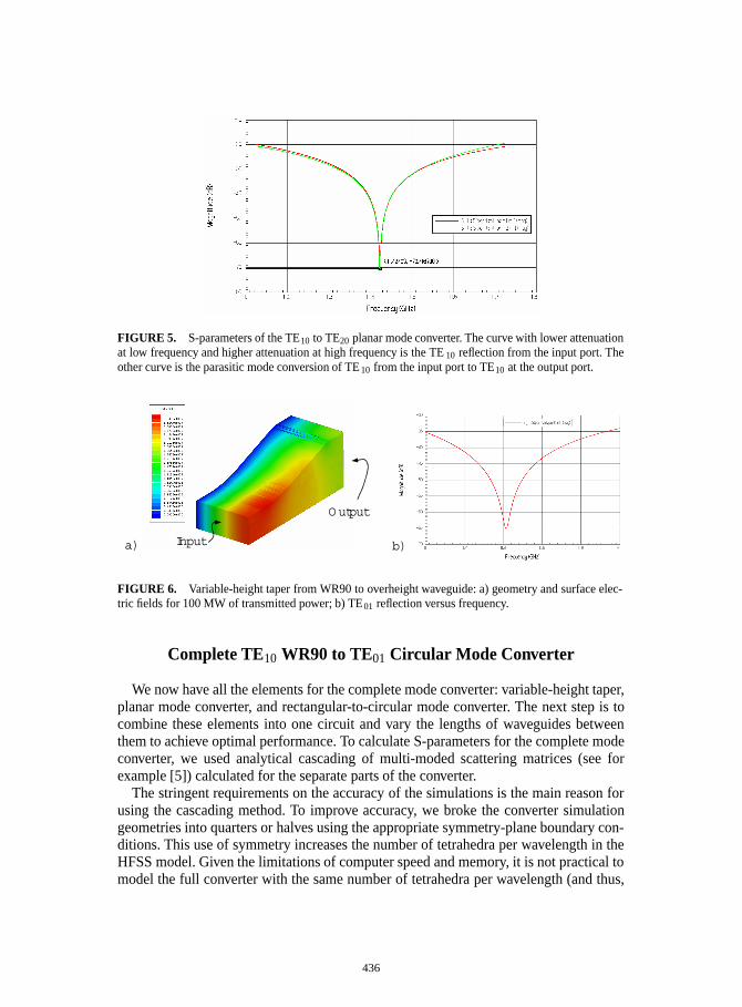
FIGURE 5. S-parameters of the TE10 to TE20 planar mode converter. The curve with lower attenuationat low frequency and higher attenuation at high frequency is the TE 10 reflection from the input port. Theother curve is the parasitic mode conversion of TE10 from the input port to TE10 at the output port.
a) b)Input
Output
FIGURE 6. Variable-height taper from WR90 to overheight waveguide: a) geometry and surface elec-tric fields for 100 MW of transmitted power; b) TE01 reflection versus frequency.
Complete TE10 WR90 to TE01 Circular Mode Converter
We now have all the elements for the complete mode converter: variable-height taper,planar mode converter, and rectangular-to-circular mode converter. The next step is tocombine these elements into one circuit and vary the lengths of waveguides betweenthem to achieve optimal performance. To calculate S-parameters for the complete modeconverter, we used analytical cascading of multi-moded scattering matrices (see forexample [5]) calculated for the separate parts of the converter.
The stringent requirements on the accuracy of the simulations is the main reason forusing the cascading method. To improve accuracy, we broke the converter simulationgeometries into quarters or halves using the appropriate symmetry-plane boundary con-ditions. This use of symmetry increases the number of tetrahedra per wavelength in theHFSS model. Given the limitations of computer speed and memory, it is not practical tomodel the full converter with the same number of tetrahedra per wavelength (and thus,
436

-10 -8 -6 -4 -2 0 2 4
-10
-8
-6
-4
-2
0
2
4
-55.
-60.
-65.
-65.
-70.-70.
-75.
-80.
-6 -4 -2 0 2 4
-10
-8
-6
-4
-2
0
2
4
-58.5-59.
-59.5-60.
-60.6
-61.
TE10 port length [m m ] TE10 port length [m m ]
TE20port length [mm]
TE20port length [mm]
a) b)
FIGURE 7. Results of the optimization of the port lengths the between WR90 variable-height taper andthe TE10 to TE20 planar mode converter (TE10 port length), and between the planar mode converter andthe TE20 rectangular to TE01 circular mode converter (TE10 port length): a) WR90 TE10 mode reflection;b) parasitic mode conversion from WR90 TE10 mode.
the same accuracy) as in the reduced geometries. Multiple simulations of the completeconverter for a two-parameter scan of the lengths of connecting waveguides does notappear to be practical either.
We wrote a Mathematica [6] program to perform the cascading analysis. First, wecalculated a frequency scan of the S-parameters for each element with each symmetrysetting and saved the data. The cascading program read the S-parameter data for allthe elements, analytically changed the length of the waveguide ports and cascaded thecorresponding transmission matrices. The results of the port length optimization areshown in Fig. 7. Reflection and parasitic mode conversion for the complete TE10 WR90to TE01 circular mode converter are shown on Fig. 8.
FIGURE 8. Reflection and mode conversion for the complete TE 10 WR90 to TE01 circular modeconverter.
437

SUMMARY
We designed two compact mode converters with lower than –50 dB parasitic mode con-version. The TE20 rectangular to TE01 circular mode converter could be a base com-ponent for high power waveguide systems that use overmoded components exclusively,with an attendant performance that would be superior to that of single-moded systems.The WR90 to TE01 circular mode converter could serve to connect overmoded systemswith existing single moded (WR90) inputs and outputs. The methodology successfullydeveloped for the design of the mode converters could be applied to create future over-moded systems, for example at different frequencies.
ACKNOWLEDGEMENT
This work was supported by the U.S. Department of Energy under contract DE-AC02-76SF00515.
REFERENCES
1. HFSS (Ansoft Corp.); available online: http://www.ansoft.com/products/hf/hfss/2. CASCADE (Calabazas Creek Research, Inc.); available online: http://calcreek.com/cascade.html3. S. G. Tantawi et al., Phys. Rev. ST Accel. Beams 8, 042002 (2005).4. S. G. Tantawi, N. M. Kroll and K. Fant, “RF components using over moded rectangular waveg-
uides for the Next Linear Collider multimoded delay line RF distribution system,” SLAC-REPRINT-1999-142, available online: http://www.slac.stanford.edu/spires/find/hep/www?r=slac-reprint-1999-142; also Proc. IEEE Particle Accelerator Conference (PAC 99), New York, New York, 29 Mar -2 Apr 1999.
5. K. Gupta and R. Cadha, Computer Aided Design of Microwave Circuits, Norwood, MA: Artech House,Inc., 1985.
6. MATHEMATICA (Wolfram Research, Inc.); available online: http://www.wolfram.com/
438