design of a flexible and modular test bed for studies on
TRANSCRIPT

Design of a Flexible and Modular
Test Bed for Studies on Islanded
Microgrids
by
Marten Pape
A thesis
presented to the University of Waterloo
in fulfillment of the
thesis requirement for the degree of
Master of Applied Science
in
Electrical and Computer Engineering
Waterloo, Ontario, Canada, 2015
© Marten Pape 2015

ii
AUTHOR'S DECLARATION
I hereby declare that I am the sole author of this thesis. This is a true copy of the
thesis, including any required final revisions, as accepted by my examiners.
I understand that my thesis may be made electronically available to the public.

iii
Abstract
The last two decades in the electric power sector have been increasingly dominated by
a rising interest in the integration of distributed energy resources (DERs) into electric
power systems, many of them based on renewable energies. A wider-scale deployment of
DERs raises questions in the design, planning and operation of electricity grids. In par-
ticular, the operational paradigms of distribution grids are about to change significantly.
One way proposed for putting small-scale DERs into the heart of an electric power
system is through realizing “Microgrids”. The concept of Microgrids proposes methods
to allow participation of DERs in main and ancillary services on the level of distribution
grids.
To foster research and development in the fields of Microgrids and grid-connected
power electronic converters, test beds with adequate functionality are required. Around
the world, many test beds have been created to allow experimentation and collection of
experiences using full-scale, real equipment and fixed network layouts. However, these
test beds are expensive, costly and large, and do not offer a high flexibility for reconfig-
uration.
Therefore, this thesis proposes, implements and evaluates a Microgrid test bed using
the Hardware-in-the-loop approach to simulate the behavior of different types of gener-
ation, energy storage and loads in a Microgrid. Identical power electronic converter mod-
ules are used to generate the currents, voltages and powers required to imitate the AC-
bus grid connection of such grid participants. Software models govern converter control
and plant simulation, allowing for a fast and flexible reconfiguration of the entire test
bed. This approach heavily cuts down cost, size and weight of test beds and allows a
much more flexible and reproducible creation and execution of test scenarios.

iv
Acknowledgements
First of all, I would like to express my deepest gratitude to my supervisor, Dr. Mehrdad
Kazerani. Without his steady and generous support, empathy, guidance and confidence,
this thesis project could not have come to anywhere close to this. I am very happy to
have had the chance to learn, experience and try many aspects of academic and practical
life during this time. His thoughts, encouragement and trust have been inspiring count-
less times. Also, I thank Dr. Bhattacharya and Dr. Salama for providing feedback to
this thesis.
I want to thank Mahmoud Allam for being such a great support as a colleague and as
a friend. He has dedicated many hours in designing and implementing the CAN protocol
stack that this thesis required. He also volunteered to take over the lead in assembling
the fourth simulation module. We spent countless hours in the lab to discuss and reflect
ideas, problems, concepts, cultures and life. The work in the lab wouldn’t even have
been half of the fun if he wouldn’t have been around.
I want to thank, Danni Luo, who has taken a lead in the assembly of the third simu-
lation module; Wenbao Hou who has helped me in quickly switching from one Micro-
controller hardware to another when it became necessary and with the assembly of the
AC breaker boxes; Zuher Alnasir, Elham Karimi and Jordan Morris for all the fun times
and input in the past years and for being in the lab at any unreasonable hour to play
‘the high-voltage backup guy’ role.
Finally, I am grateful for great artists that stimulated great inspiration, relief, concen-
tration and joy. Especially, I would like to thank for your presence and work to: Herman
van Veen, Avishai Cohen, Chick Corea, Diana Krall, Habanot Nechama, John Surman,

v
Jan Gabarek, Stephan Micus, Xavier Rudd, Ketil Bjørnstad, David Darling, Xavier Nai-
doo, Trygve Seim, Norah Jones, Thomas Carbou, Sting, Bobby McFerrin, Anứna and
Maybebop. Life is full of art and spirit. There is no life without it.

vi
Dedication
“We did not inherit this world from our parents …
We are borrowing it from our children.”
It is my fervent hope that the engineers, scientists, politicians, policy makers and
ordinary people of today will dedicate themselves to the creation of a world where chil-
dren and grandchildren will be left with air they can breathe and water they can drink,
where humans and the rest of nature will nurture one another.
In dependence on Robert A. Messenger and Jerry Ventre – Photovoltaic Systems
Engineering, Third Edition, CRC Press, 2010
To Heather, who has such an incredible sense for this air we breathe, the water we drink
and our neighbors on earth; no matter how tiny or huge.

vii
Table of Contents AUTHOR'S DECLARATION ................................................................................... ii
Abstract .................................................................................................................... iii
Acknowledgements .................................................................................................... iv
Dedication ................................................................................................................ vi
Table of Contents .................................................................................................... vii
List of Figures ........................................................................................................ xiv
List of Tables ........................................................................................................... xx
Chapter 1 Introduction.............................................................................................. 1
1.1 Motivation ..................................................................................................... 1
1.1.1 Research on Microgrids ........................................................................... 1
1.1.2 Test beds in research and development .................................................. 3
1.1.3 Required test environments for the advancement of Microgrids and its
components .............................................................................................................. 4
1.2 Background information ................................................................................ 6
1.2.1 Hardware-in-the-loop .............................................................................. 6
1.3 Existing test bed approaches ......................................................................... 7
1.4 Microgrid test bed goal definition .................................................................. 9
1.5 Thesis organization ...................................................................................... 11
Chapter 2 Background review ................................................................................. 13
2.1 Common converter topologies for low-voltage grid applications ................. 13
2.2 Converter output filter for grid-connected VSI ........................................... 17
2.3 Control objectives for grid interfacing converters ........................................ 18
2.3.1 Grid-forming converters ........................................................................ 19
2.3.2 Grid-feeding / grid-following converters ............................................... 19
2.3.3 Grid-supporting converters ................................................................... 20

viii
2.4 Control in the synchronous reference frame ................................................ 22
2.4.1 The abc-dq0 transformation ................................................................. 22
2.4.2 The dq0 controller block ....................................................................... 24
2.4.3 Decoupling of d and q channels ............................................................ 25
2.4.4 Feed-forward terms ............................................................................... 26
2.4.5 Controller output limiting ..................................................................... 26
2.5 Control in the stationary reference frame .................................................... 28
2.6 Phase-locked loops for grid application ....................................................... 30
2.7 Voltage-source based droop control ............................................................. 31
2.7.1 Droop control for grid-supporting converters ....................................... 31
2.7.2 Virtual impedance ................................................................................. 33
2.7.3 Power droop decoupling due to X/R ratio ........................................... 34
2.7.4 Negative sequence control ..................................................................... 35
2.8 Control of direct parallel connected 3-phase inverters ................................. 37
2.8.1 Using ΔY transformers ......................................................................... 37
2.8.2 Using four converter legs and zero sequence current control ................ 39
Chapter 3 Test bed system structure design ........................................................... 46
3.1 System component arrangement .................................................................. 46
3.1.1 System component sizing ...................................................................... 49
3.1.2 AC Microgrid voltage ............................................................................ 50
3.1.3 DC-bus voltage ..................................................................................... 50
3.1.4 Communication link .............................................................................. 51
Chapter 4 Simulation module hardware design ....................................................... 53
4.1 Simulation module structure ....................................................................... 53
4.2 Power circuit design ..................................................................................... 54
4.2.1 Power switches ...................................................................................... 55

ix
4.2.2 Controllable breakers ............................................................................ 58
4.2.3 Converter output filter .......................................................................... 59
4.3 Control circuit design .................................................................................. 60
4.3.1 Sensors .................................................................................................. 60
4.3.2 Simulation module control unit (SMCU) – Microcontroller ................. 63
4.3.3 Low voltage power supply ..................................................................... 65
4.4 Derivation of a DC-bus voltage controller module ...................................... 65
4.4.1 Requirements ........................................................................................ 65
4.4.2 Module structure ................................................................................... 66
4.4.3 Control of DC-bus voltage .................................................................... 69
4.4.4 Simulation results ................................................................................. 71
4.5 Mechanical setup of Microgrid test bed ....................................................... 74
4.6 Cost analysis ................................................................................................ 76
4.7 Design summary .......................................................................................... 76
Chapter 5 Grid interfacing control topologies ......................................................... 77
5.1 Interface definition for grid interfacing control topologies (Hardware-in-the-
loop interface). .......................................................................................................... 78
5.1.1 Energy conversion system to grid interface .......................................... 78
5.1.2 Software interface: control topology to inverter .................................... 82
5.2 Grid following controller .............................................................................. 82
5.2.1 Control objective ................................................................................... 82
5.2.2 Common use ......................................................................................... 82
5.2.3 Realization ............................................................................................ 83
5.2.4 Simulation results ................................................................................. 86
5.3 Voltage-source based droop controller ......................................................... 88
5.3.1 Control objective ................................................................................... 88

x
5.3.2 Common use ......................................................................................... 88
5.3.3 Realization ............................................................................................ 88
5.3.4 Simulation results ................................................................................. 92
5.4 Current-source based droop controller ......................................................... 97
5.4.1 Control objective ................................................................................... 97
5.4.2 Common use ......................................................................................... 97
5.4.3 Realization ............................................................................................ 97
5.4.4 Simulation results ................................................................................ 101
Chapter 6 Load and generation plant modelling .................................................... 103
6.1 Introduction ................................................................................................ 103
6.2 Load model ................................................................................................. 104
6.3 Photovoltaic plant model ............................................................................ 105
6.3.1 Objective and simplifications ............................................................... 105
6.3.2 Model structure .................................................................................... 105
6.3.3 Mathematical formulation .................................................................... 108
6.3.4 Implementation .................................................................................... 116
6.4 Storage plant model .................................................................................... 116
6.4.1 Objective .............................................................................................. 116
6.4.2 Mathematical formulation .................................................................... 117
Chapter 7 Test bed simulation using a circuit simulator ....................................... 120
7.1 Simulation setup ......................................................................................... 121
7.2 Load and solar insolation profiles ............................................................... 123
7.3 Results ........................................................................................................ 123
Chapter 8 Software design for simulation module firmware ................................... 127
8.1 Design goals and design principles .............................................................. 127
8.2 Review: software design patterns ................................................................ 129

xi
8.2.1 Hardware proxy pattern ....................................................................... 129
8.2.2 Hardware adapter pattern ................................................................... 129
8.2.3 Observer pattern .................................................................................. 130
8.2.4 Asynchronous, single-event receptor state machine ............................. 132
8.3 Performance considerations ........................................................................ 134
8.4 Code portability .......................................................................................... 135
8.5 Implementation ........................................................................................... 137
8.5.1 Hardware abstraction ........................................................................... 138
8.5.2 Scheduling ............................................................................................ 138
8.5.3 Example: Control loop execution program flow ................................... 140
8.5.4 Program state management ................................................................. 141
8.5.5 Global settings storage ......................................................................... 143
8.5.6 Controller and plant model abstraction ............................................... 144
8.5.7 Software-based circuit protection ......................................................... 146
8.5.8 Additional software components .......................................................... 147
8.5.9 CAN communication ............................................................................ 147
8.6 Summary ..................................................................................................... 149
Chapter 9 Software design: Test bed central controller ......................................... 150
9.1 Design goals ................................................................................................ 150
9.2 Design patterns ........................................................................................... 151
9.3 Architectural choices ................................................................................... 152
9.3.1 Programming language and framework ............................................... 152
9.3.2 Program module interfacing ................................................................ 152
9.3.3 Threading model .................................................................................. 154
9.4 Implementation overview: Model ................................................................ 155
9.4.1 CAN communication ............................................................................ 156
xii
9.4.2 MicrogridModule, SimulationModule, DcBusModule .......................... 156
9.4.3 Microgrid module management............................................................ 157
9.4.4 Grid interfacing control loops .............................................................. 157
9.4.5 Plant models ........................................................................................ 158
9.4.6 Measurements ...................................................................................... 158
9.4.7 Profile service, command file execution ............................................... 159
9.4.8 Global simulation controller ................................................................. 160
9.4.9 Logging ................................................................................................ 161
9.5 Implementation overview: View .................................................................. 162
9.5.1 Main window ........................................................................................ 162
9.5.2 SimulationModule, DcBusModule, control loops, plant models .......... 163
9.5.3 Measurements, plotting ........................................................................ 164
9.5.4 Global simulation control ..................................................................... 164
9.6 Interfacing a secondary controller algorithm .............................................. 164
9.7 Summary ..................................................................................................... 165
Chapter 10 Experimental results ............................................................................ 166
10.1 Grid-following converter .......................................................................... 166
10.2 Grid-supporting converter ....................................................................... 170
10.2.1 Voltage-source based droop controller .............................................. 170
10.2.2 Current-source based droop controller ............................................. 177
10.3 Load plant model .................................................................................... 180
10.4 Photovoltaic plant model ........................................................................ 182
10.4.1 Normal PV model operation ............................................................ 182
10.4.2 Operation with PV curtailment ....................................................... 184
10.5 DC-bus voltage controller module ........................................................... 187
10.6 Simulation of a 24-hour grid scenario on the test bed ............................ 191

xiii
10.7 Summary ................................................................................................. 195
Chapter 11 Conclusions .......................................................................................... 196
Chapter 12 Future work ......................................................................................... 199
A.1 Virtual impedance in synchronous reference frame for voltage-source based
droop controllers....................................................................................................... 201
Bibliography ........................................................................................................... 254

xiv
List of Figures Figure 1.1 General HIL, Controller HIL and Power HIL (left to right) [6] ............... 7
Figure 2.1 Three-Phase voltage-source inverter topology ....................................... 14
Figure 2.2 Current-source inverter .......................................................................... 16
Figure 2.3 L-filter .................................................................................................... 17
Figure 2.4 LC-filter .................................................................................................. 17
Figure 2.5 LCL-filter ............................................................................................... 17
Figure 2.6 Grid-forming controller representation ................................................... 19
Figure 2.7 Grid-feeding controller representation .................................................... 20
Figure 2.8 Droop curves for P/f and Q/V droop .................................................... 21
Figure 2.9 Current-source based droop controller representation ........................... 22
Figure 2.10 Voltage-source based droop controller representation .......................... 22
Figure 2.11 dq0 controller block structure .............................................................. 24
Figure 2.12 Single phase representation of a converter output LCL filter .............. 25
Figure 2.13 Three-phase synchronous reference frame PLL structure .................... 30
Figure 2.14 Single-phase synchronous reference frame PLL structure .................... 31
Figure 2.15 General controller structure for voltage-source based droop controlled
converters ...................................................................................................................... 32
Figure 2.16 Virtual impedance ᵃ�ᵃ� ......................................................................... 33
Figure 2.17 Two direct parallel connected 3-phase VSIs using Δᵃ� transformers ... 37
Figure 2.18 Two direct parallel connected 3-phase VSIs with four legs and not
transformer ................................................................................................................... 40
Figure 2.19 ZSC current control based on modified SVM. Depicted: Instantaneous
leg voltages between ᵃ�ᵃ�ᵃ� and ground for one switching cycle in a three-leg inverter. . 42
Figure 2.20 ᵃ�ᵅ�ᵃ� for traditional PWM for a single inverter ..................................... 42
Figure 3.1 Overall Microgrid test bed structure...................................................... 46

xv
Figure 4.1 Simulation module structure .................................................................. 54
Figure 4.2 NTC temperature sensing circuit ........................................................... 57
Figure 4.3 Implementation IGBTs, IGBT drivers and thermal management ......... 57
Figure 4.4 AC breaker box (inside view) ................................................................. 59
Figure 4.5 Single-phase stage of three-phase sensor board ...................................... 61
Figure 4.6 AC sensor implementations. Some transducers on bottom side of PCB.62
Figure 4.7 Microcontroller adapter board developed for TMS320F28377D
experimenter kit. Experimenter kit underneath adapter board. .................................. 64
Figure 4.8 DC-bus voltage controller module structure. ......................................... 66
Figure 4.9 DC-bus charge/discharge circuit ............................................................ 68
Figure 4.10 Control loop topology of DC-bus voltage controller module ................ 69
Figure 4.11 DC-bus voltage controller module simulation: (a) ᵃ�ᵃ�ᵃ� under full
operation cycle; (b) AC power (blue) and DC power (red) .......................................... 72
Figure 4.12 ᵃ�ᵃ�ᵃ� ripple and transients under no load and full load ......................... 72
Figure 4.13 ᵃ�ᵃ�ᵃ� ripple and transients at simulation module 10 (blue) and at DC-bus
voltage controller module (red, mostly hidden) ............................................................ 73
Figure 4.14 AC currents when DC-side load goes through a step change from 0% to
100% power rating ........................................................................................................ 74
Figure 4.15 Mechanical layout of a shelf for two simulation module converters ..... 75
Figure 5.1 Generalization of plant structures .......................................................... 78
Figure 5.2 Definition of HIL interface between plant model and grid interface ...... 81
Figure 5.3 Control loop structure using dq0 PI controllers for grid-following
converters ...................................................................................................................... 83
Figure 5.4 Active and reactive power injection upon power reference steps for P & Q
...................................................................................................................................... 87

xvi
Figure 5.5 Output currents ᵅ�ᵅ�, ᵃ�ᵃ�ᵃ� upon a reference step from P=0W to P=5000W
(Q=0) ........................................................................................................................... 87
Figure 5.6 Basic voltage-source based droop controller implementation ................. 89
Figure 5.7 Complete voltage-source based droop controller implementation .......... 90
Figure 5.8 Voltage-source based droop controller: stand-alone simulation block
structure ....................................................................................................................... 92
Figure 5.9 Inverter capacitor voltages (a) and output currents (b) when PQ load step
change from 0W to 2500W is performed ...................................................................... 94
Figure 5.10 Inverter output power and PQ power load references (a) and inverter
output currents (b) for entire load schedule ................................................................. 94
Figure 5.11 Voltage-source based droop controller: power sharing simulation block
structure ....................................................................................................................... 95
Figure 5.12 Power sharing between two voltage-source droop controllers under
varying load conditions ................................................................................................. 96
Figure 5.13 Current-source based droop controller implementation ....................... 99
Figure 5.14 Simulation configuration ..................................................................... 101
Figure 5.15 System parameters in a simulation with one voltage-source based droop
controller (module 2) and one current-source based droop controller (module 1) in
parallel ......................................................................................................................... 102
Figure 6.1 Structure of the PV plant implemented ................................................ 106
Figure 6.2 PV model simulation in PSIM vs. computation in implemented C++
model for Bosch c-SI M2453BB PV module ................................................................ 111
Figure 6.3 Definition of ᵃ�1, ᵃ�2 and ᵃ�3 at the example of discontinuous inductor
current ......................................................................................................................... 112
Figure 6.4 Comparison of average model with circuit simulation. Blue: ᵃ�ᵅ�ᵅ�ᵅ� average
model; red: ᵃ�ᵅ�ᵅ�; Green: ᵃ�ᵅ�ᵅ�ᵅ� PSIM simulation ........................................................... 114
xvii
Figure 6.5 HIL grid interface block structure ......................................................... 115
Figure 6.6 Basic operation principle of generic storage plant ................................ 119
Figure 7.1 PSIM test bed system simulation – main page ..................................... 122
Figure 7.2 Solar insolation and load profile for 24 hours ....................................... 123
Figure 7.3 Active power injections into grid (a), Microgrid system frequency (b) and
Microgrid RMS voltage (c) over the 24-hour profile .................................................... 125
Figure 7.4 PV plant model internal variables: power flow (a) and ᵃ�ᵃ�ᵃ� (b) ........... 126
Figure 7.5 SOC of both storage plants ................................................................... 126
Figure 8.1 Program structure of SMCU firmware .................................................. 137
Figure 8.2 Scheduling of non-critical tasks. Realized by TaskScheduler ............... 139
Figure 8.3 Work flow ADC-ISR critical code execution ......................................... 140
Figure 8.4 DcAcOperationController states for simulation module ...................... 142
Figure 8.5 AcDcOperationController states for DC-bus voltage controller module
..................................................................................................................................... 142
Figure 8.6 PI controller implementation with output limitation, scaling and external
offset ............................................................................................................................ 145
Figure 9.1 TBCC software structure with focus on CAN protocol stack ............... 153
Figure 9.2 TBCC ‘model’ block structure .............................................................. 155
Figure 9.3 States of global simulation control ........................................................ 160
Figure 9.4 TBCC ‘view’ block structure ................................................................ 162
Figure 10.1 Grid-following converter test configuration ......................................... 167
Figure 10.2 Grid-following control topology: transient performance ...................... 168
Figure 10.3 Grid-following control topology: steady state, four quadrant performance.
..................................................................................................................................... 169
Figure 10.4 (a) ᵅ�ᵅ�, ᵃ�ᵃ� for droop controlled module during load profile defined for test
case 1. .......................................................................................................................... 172

xviii
Figure 10.5 Two voltage-source droop controlled modules in operation. ............... 174
Figure 10.6 (a)-(d): test case 1. (e)-(h): test case 2 ............................................... 175
Figure 10.7 Voltage-source based droop controller voltages. .................................. 177
Figure 10.8 : ᵅ�ᵅ�, ᵃ�ᵃ� for voltage-source based droop controlled module during load
profile defined for test case 1. ...................................................................................... 178
Figure 10.9 System voltage (a), frequency (b) and power flow (c)-(d) in a current-
source based droop and voltage-source based droop controlled islanded test grid ...... 179
Figure 10.10 Load plant model performance. ......................................................... 181
Figure 10.11 PV plant model variables at a solar insolation step change from
50 ᵃ�/ᵅ�2 to 300 ᵃ�/ᵅ�2. ............................................................................................ 183
Figure 10.12 Solar insolation step from 50 ᵃ�/ᵅ�2 to 300 ᵃ�/ᵅ�2 and back. ......... 184
Figure 10.13 Solar insolation step change from 50 ᵃ�/ᵅ�2 to 600 ᵃ�/ᵅ�2 and back.
ᵃ�ᵅ�ᵃ�ᵅ� = 5000ᵃ� . .......................................................................................................... 186
Figure 10.14 Solar insolation step change from 50 ᵃ�/ᵅ�2 to 600 ᵃ�/ᵅ�2 and back.
ᵃ�ᵅ�ᵃ�ᵅ� = 2000ᵃ� . .......................................................................................................... 187
Figure 10.15 DC-bus voltage ripples under different loading conditions. ............... 189
Figure 10.16 DC-bus voltage (blue) during load power step change (0W to 5000W).
..................................................................................................................................... 190
Figure 10.17 DC-bus voltage during full operating cycle: ...................................... 190
Figure 10.18 24-hour simulation: power flows. ....................................................... 192
Figure 10.19 24-hour simulation: PV plant variables ............................................. 193
Figure 10.20 24-hour simulation: PV plant DC-bus voltage (zoom) ...................... 194
Figure 10.21 24-hour simulation: storage module SOC during the day ................. 194
Figure A.1 Converter output circuit with virtual impedance ................................ 201

xix
Figure A.2 VSI output filter circuit connected to AC Microgrid, single-line diagram.
..................................................................................................................................... 205
Figure A.3 Required ᵃ�ᵃ� for different complex power injections ............................. 206
Figure A.4 DC-bus charge/discharge circuit .......................................................... 206
Figure A.5 ᵃ�ᵅ�ᵅ�ᵅ�ᵅ� power consumption (a) and ᵃ�ᵃ�ᵃ� overshoot (b) ......................... 209
Figure A.6 Basic (ideal) circuit of a buck-boost converter ..................................... 211
Figure A.7 Definition of ᵃ�1, ᵃ�2 and ᵃ�3 (example: inductor current discontinuous)
..................................................................................................................................... 213
Figure B.1 IPM circuit with snubbers, protection, temperature sensor, fan and PWM
control .......................................................................................................................... 216
Figure B.2 AC breaker power circuit schematic ..................................................... 217
Figure B.3 AC breaker board schematic ................................................................ 218
Figure B.4 Three-phase sensor board, complete schematic .................................... 220
Figure C.1 The TBCC main window with multiple modules online ...................... 237
Figure C.2 SimulationModuleUI (a) and DcBusModuleUI (b) ................................. 237
Figure C.3 Example plot of a measurement of a PV plant variable ...................... 238
Figure C.4 Profile command display window with six commands loaded .............. 238
Figure C.5 Configuration dialog for the voltage-source based droop controller (a), PV
module parameter estimation after [63], [66] (b) ......................................................... 239

xx
List of Tables Table 4.1 Default parameterization of module’s control loops ................................ 70
Table 4.2 Total Microgrid test bed cost (incl. DC-bus voltage controller module and
four simulation modules) .............................................................................................. 76
Table 5.1 Parameters of grid-following converter control loop topology ................. 85
Table 5.2 Simulation load power references ............................................................. 86
Table 5.3 Parameters of voltage-source based droop controller topology ............... 90
Table 5.4 PQ load schedule ..................................................................................... 92
Table 5.5 Parameters of current-source based droop controller topology .............. 100
Table 6.1 Nomenclature for PV cell model ............................................................ 108
Table 6.2 Nomenclature for storage plant model ................................................... 118
Table 7.1 Test bed simulation configuration .......................................................... 121
Table 10.1 Load power references for test case 1 ................................................... 172
Table 10.2 ZIP load configuration for presented test case ..................................... 180
Table 10.3 PV model key parameters ..................................................................... 182

Chapter 1
Introduction
1
Chapter 1
Introduction
1.1 Motivation
1.1.1 Research on Microgrids
The last two decades in the electric power sector have been increasingly dominated by
a rising interest in the integration of distributed energy resources (DERs) into electric
power systems. Among DERs, many conversion types are based on renewable energy
resources, such as photovoltaic energy conversion, wind power, geothermal energy or
biomass. Increasing interest in the reduction of greenhouse gas (GHG) emissions and
intensified research and innovation in the aforementioned conversion technologies have
allowed for a wider-scale deployment, accompanied by declining deployment cost.
The traditional power system is dominated by a limited number of large-scale hydro-
thermal generation plants connected to transmission grids with customers typically con-
nected to distribution grids. With the large-scale deployment of DERs, fundamental
changes in the power system architecture become more relevant the higher the penetra-
tion levels of DERs become. DERs offer prominent advantages when placed close to the
customer and can be scaled more efficiently in much wider ranges than is possible in the

Chapter 1
Introduction
2
case of large-scale hydro-thermal plants. As a result, there is an increasing need to inte-
grate these distributed and small-scale resources into electricity grids with a reasonable
system efficiency and system cost.
One way proposed for putting small-scale DERs into the heart of an electric power
system is through realizing “Microgrids”, a concept first introduced in [1], [2]. The initial
definition for a Microgrid was given as: “A Microgrid is a cluster of micro-sources, storage
systems and loads which presents itself to the grid as a single entity that can respond to
central control signals” [1]. In contrast with the traditional setup of electric power sys-
tems, a Microgrid puts generation, storage and loads in potentially identical layers of
grids reflecting the common deployment of DER unit in distribution grids. It can be
operated in two modes: grid-connected and islanded. The grid-connected mode allows a
Microgrid to interact with a main grid by using services of and providing services to the
main grid at its point of common coupling (PCC). This is mostly interesting when ap-
plying the Microgrid concept to locations with already existing interconnected power
systems. In the islanded mode of operation, this exchange of services with a main grid
is not possible and a Microgrid has to provide all necessary services for a stable and
efficient operation from within itself. Islanded operation can be intentional or uninten-
tional. This capability can help to increase system reliability and resilience. It can also
enable a larger-scale deployment of many DER units in stand-alone power systems, as
used in remote communities, for example.
In order to ensure proper control of all relevant quantities in a Microgrid, various
Microgrid control approaches have been proposed. Most notably, three categories can be
defined: centralized control, decentralized control and hierarchical control.
“A fully centralized control relies on the data gathered in a dedicated central controller
that performs the required calculations and determines the control actions for all the

Chapter 1
Introduction
3
units at a single point, requiring extensive communication between the central controller
and controlled units. On the other hand, in a fully decentralized control, each unit is
controlled by its local controller, which only receives local information and is neither
fully aware of system-wide variables nor other controllers’ actions” [3].
To mitigate some of these concepts’ disadvantages, a combination of the aforemen-
tioned approaches has been established: hierarchical control. For Microgrids, three to
four control hierarchy levels are commonly defined [4]. Level zero is concerned with local
control of current and voltage of a single unit. The primary control level is realized in
each generation unit employing droop-control methods or similar methods to control
voltage and frequency in a stable manner at the PCC without relying on signals not
locally available. The secondary control level can provide frequency and voltage restora-
tion to nominal values, economical operation [3] and resynchronization to grid-connected
mode. This level is typically implemented as a central controller. The tertiary control
level then allows controlling power flow between the Microgrid and other interconnected
(Micro-) grids.
The concept of Microgrids has the potential to enable a wide-scale deployment of
renewable DERs at high penetration levels from a grid perspective, since it addresses all
main operational issues with (renewable) DERs the power industry is facing today.
1.1.2 Test beds in research and development
Test beds are an essential tool in the development of new technical concepts and the
refinement of existing methods. A test bed allows to conduct extensive, reproducible and
transparent tests on a technical concept in pre-defined environments outside of an envi-
ronment that could unintentionally cause harm to people or damage to equipment. Test
beds can be used in many roles during a research and development process and even

Chapter 1
Introduction
4
after deployment of the developed technique. It becomes possible to verify a concept at
full dynamic order on a system that (closely) replicates real environments and therefore
unveils problems that might be hidden due to assumptions and simplifications induced
by assumed model simplification. Test beds serve as demonstrators of concepts to tech-
nical and non-technical audiences and allow the verification of proper functionality of
different concepts in a standardized environment or to verify a proper change of scope
in the application of an existing concept. Lastly, test beds have also been used during
the operation of a product to reproduce and examine incorrect behaviour in a safe envi-
ronment observed during the product life cycle. For example, this is a common tool in
space missions.
Since the Microgrid concept promotes a grid structure with fundamental differences
with respect to the existing grid, with high initial and running cost and potential impact
on the reliability of the electric power grid, there have to be extensive, flexible and high-
quality test bed environments to advance techniques for the Microgrid environment.
High complexity in proposed control architectures (level zero up to tertiary level) require
a tool for testing, examination, verification and demonstration across multiple control
hierarchies.
1.1.3 Required test environments for the advancement of Mi-
crogrids and its components
Matlab/Simulink, PSIM, Spice, PSCAD and PowerWorld are commonly used tools to
replicate behaviour of grids at component and system levels in software. These tools
allow a fast implementation and reconfiguration of the test environment at very low cost.
Therefore, these tools are among the most popular ways to test and support developing

Chapter 1
Introduction
5
new concepts. However, software tools come with certain limitations. Simulation of com-
ponents or systems is based on the model representation of the sub-components used in
a system. These models are often subject to a trade-off between accurate replication of
reality in all relevant environments, model complexity and execution speed. Limitations
arise when both, the system complexity and the level of simulation details is high, avail-
able computational power is limited, the description of reality with models cannot be
accurately achieved enough or too many uncertainties exist. Finally, proving the full
viability of a concept becomes easier and more credible the closer the simulation is to a
real case.
To mitigate previously mentioned disadvantages of software-based simulation, hard-
ware-based test beds1 are being used. These simulators allow the replication of test cases
in an environment that is exactly the same as or very close to a production environment.
Test beds can show the full system dynamics at real-time and high system complexity
without being (much) reliant on model representations of reality. Test beds allow verifi-
cation of basic assumptions in developed concepts and modeling applied in software-
based simulations. They can be a natural evolution from software models towards a final
product or concept. However, test beds for electricity grids tend to be costly, large in
size and weight, and limited in the ability to reconfigure the test-setup. The development
of a test bed can bind many resources and take an incomparable long time compared to
software-based simulators.
Therefore the goal of this thesis is to develop a test bed usable in the research on
Microgrid systems and Microgrid components that is:
1. Easily reconfigurable and expandable
1 From now on just referred to as “test beds”

Chapter 1
Introduction
6
2. Low in construction and operation cost
3. Able to capture the full system dynamics for Microgrid operation relevant
topics from as small as power electronic switching events to as high-level as
Microgrid power exchange.
More specifications on this goal, basic assumptions and limitations are given in section
1.4.
1.2 Background information
1.2.1 Hardware-in-the-loop
The hardware-in-the-loop (HIL) concept is relatively new, allowing for fast but close-to-
reality test methods by combining software-based simulations with selected hardware-
based simulations. The principle is to run real-time simulations in software, where accu-
rate and good models exist, and include a hardware stage into the simulation, where
models are inaccurate, hard to obtain or very complicated [5]. A software simulator
interfaces a hardware-based device under test (DUT) using digital-to-analog converters
and sensors for the return path (Figure 1.1). To test a controller performance, the con-
cept of controller hardware-in-the-loop (CHIL) can be applied. In this case, a controller
would be executed in the loop with a software model. More interestingly, to test power
hardware equipment together with software models in real-time, power hardware-in-the-
loop (PHIL) can be applied. In PHIL, the interface is supplemented with a power am-
plifier stage to provide the required output power needed to realize quantities from
within the software model on the power device under test [6].

Chapter 1
Introduction
7
Figure 1.1 General HIL, Controller HIL and Power HIL (left to right) [6]
Special considerations in HIL tests have to be made on the hardware interfacing
software and DUT. Digital-to-analog converters and sensors with an infinite bandwidth,
resolution, accuracy and output power and zero noise do not exist. Non-ideal sensors
and sensor interfaces can introduce errors into the simulation that are significant to the
simulation results. Especially in PHIL simulations, the power interface - typically con-
sisting of linear power amplifiers and power sensors - can introduce significant delays
into the system, affecting stability and controller configurations [5]. Proper selection of
the interfacing signals is therefore critical to the simulation performance.
1.3 Existing test bed approaches
Many Microgrid test beds have already been implemented around the world. Some test
beds are designed as research and development tools; others are more focused on demon-
stration and validation purposes[7]–[18]. Most setups employ commercial products, such
as photovoltaic plants, wind turbines, gas generators, battery or flywheel storage sys-
tems, fuel cells or diesel generators. These approaches offer the closest simulation of real
scenarios in many terms, since no model abstractions are employed. Since all parts of a
Software basedsimulator
Device undertest
D/A A/D
A/D D/A
Software basedsimulator
Controller undertest
D/A A/D
A/D D/A
Power deviceunder test
A/D D/A
Software basedsimulator
D/A A/D
Power Interface

Chapter 1
Introduction
8
Microgrid are realized with components used in production environments, all pending
issues either have to be overcome or will appear while implementing such a test bed.
Power ratings of the generators used are often in the range of 10s to 100s of kilowatts.
For example, British Columbia Institute of Technology’s Microgrid test bed employs two
5kW wind turbines, 300kW of photovoltaic models, thermal generation of 250kW and
550kWh of battery storage [19]. This sizing allows good estimations on project cost and
specific restrictions with high-voltage, high-power components.
However, the size and cost of these components are remarkable for research and devel-
opment projects and do not allow for a very wide-spread deployment of these testing
facilities. For example, the cost for a Microgrid application project of comparable size
has been reported to be at about $US 15 million [20]. Furthermore, test beds that use
real generators for renewable energy sources are dependent on the availability of primary
energy, such as solar insolation or wind, which makes these test beds weather-dependent.
This heavily impacts the reproducibility of simulations. For all setups using real gener-
ators, it is also true that the operating cost of such a test bed is considerable since all
the energy that is circulated in the test bed is consumed by dummy loads.
Finally, the network layout used to implement a Microgrid test bed is often fixed ([11]–
[14], [17], [18]). While this allows to perform case studies on specific similar grid setups,
achieving generalized tests and comparability between different setups is difficult to
achieve. For example, this is the case for the CERTS Microgrid test bed installed near
Columbus, Ohio, United States. The feeders of this setup incorporate multiple feeder
loops to simulate the impedance of long feeders [21].
To overcome the disadvantages of large size, high initial cost, limited flexibility in grid,
load and generator configurations and dependence on environmental conditions for re-
producibility, a test bed based on the hardware-in-the-loop concept has been proposed

Chapter 1
Introduction
9
and implemented [22]. This test bed consists of a set of voltage source inverters, a battery
bank, resistive loads, a bus bar matrix and a main grid connection. The computation of
generator control algorithms and generator dynamics (wind, solar…) is performed in
software whereas the grid and the power stage of grid interfaces, based on voltage-source
inverters (VSI), is implemented in hardware. This concept adds the flexibility to simulate
a Microgrid with a flexible selection of generators, such as diesel generators, photovoltaic
plants or wind turbines. Reconfiguration only requires an exchange of software models.
This setup widely overcomes the aforementioned disadvantages with conventional Mi-
crogrid test beds, adding significant flexibility to the simulation platform and reducing
cost. However, this test bed still employs some real components, such as resistive load
banks and a battery system. This means that some of the energy circulated in the test
bed to simulate a scenario is still consumed and has to be paid for. According to [23], in
this setup, it is necessary to select two AC/DC converters to form a back-to-back con-
verter configuration in order to allow active power absorption from the simulated grid.
This case would be required when modeling loads, storage-equipped DERs or pure stor-
age devices using VSI modules. Furthermore, no implementation of grid impedance rep-
resentation has been reported.
1.4 Microgrid test bed goal definition
The goal of this thesis is to develop a flexible, simple, laboratory size research tool to
provide a scalable Microgrid hardware simulation for islanded operation.
A finished test bed should provide primary simulation capabilities for:
1. Grid interface controllers. “Component-level scope”. Various methods of con-
trolling currents, voltages and power injection by a generator exist for many

Chapter 1
Introduction
10
purposes. A detailed study of these controller topologies should be possible with-
out simplifications.
2. Management of Microgrid components. “System-level scope”. Secondary
and tertiary control levels in a Microgrid are about the management of many
participants in a Microgrid. Interfaces for implementing user-defined algorithms
should be available.
The simulation of generator characteristics in software models should be as accurate
as required to produce correct behavior on the AC terminals of a simulated generator.
Furthermore the following topics are to be considered in the design of this test bed:
1. Ability to connect other components to the test bed. This can allow
studies on controller design, controller topology compatibility and grid-inter-
facing power electronic converter design
2. Ability to combine various grid interfacing mechanisms with different
generator models. Research on Microgrids has stimulated innovations in con-
trol algorithms for grid-connected inverters. It is of interest to provide this
ability to study technical and economic feasibility of various control algorithms
on different kinds of generation.
Compared to the goal definition for a finished test bed, this thesis assumes certain sim-
plifications:
1. All Microgrid generators and loads connect to a single PCC, no network im-
pedances and layouts are considered

Chapter 1
Introduction
11
2. Grid interface control algorithms assume a balanced grid. Single-phase opera-
tion is to be prepared in hardware, but not fully implemented in software and
grid interface control topologies
Therefore, this thesis presents a Microgrid test bed platform based on the hardware-
in-the-loop concept. It provides four VSI modules (“simulation modules”) of identical
design to provide an AC terminal representation of various grid components. These
components are a load emulation, a photovoltaic plant emulation and generic storage
modules. However, the platform is designed in a way that allows the implementation of
a much wider range of plant models and grid interfaces. Each simulation module is rated
at 5kVA and standard North American low-voltage distribution system voltages. This
test bed reduces the hardware complexity required for the HIL simulation compared to
[22], [23], increases flexibility by providing a common DC-bus for all simulation modules
and removes all resistive loads and storage batteries through software emulation, which
reduces the amount of energy required for a Microgrid simulation.
Software in simulation modules and on a central control computer allows the complete
reconfiguration of all major parameters in the Microgrid, including selected generator
models and grid interfacing algorithms.
1.5 Thesis organization
In the following chapters, different aspects are presented that are required to design,
implement and test the proposed Microgrid test bed.
Chapter 2 introduces key concepts that are required for the realization of this test
bed. Some technological choices are made in this chapter, as well.

Chapter 1
Introduction
12
Chapter 3 deals with the overall system structure of the proposed test bed and defines
key requirements for it. In Chapter 4, the focus is on the structure and design of a
‘simulation module’ which represent one Microgrid participant, such as a generator or a
load. Chapter 5 presents the control of these simulation modules with respect to their
Microgrid AC-bus connection. All control topologies are verified in simulation, with ex-
periments on them following later in Chapter 10.
In Chapter 6 modeling of generators and loads is given that is finally used in the
software controlling each simulation module.
The test bed design phase is concluded with computer simulations of the entire test
bed on a 24 hour load and generation profile in Chapter 7.
Chapter 8 and Chapter 9 discuss implementation-specific issues in the software used
to control the test bed (central control) and single simulation modules. The focus is to
give the overall design requirements and approaches.
Finally, Chapter 10 presents experimental results from the actual test bed to verify
proper design and implementation.
Chapter 11 and Chapter 12 close this thesis with conclusions and recommendations
for future work.

Chapter 2
Background review
13
Chapter 2
Background review
2.1 Common converter topologies for low-voltage
grid applications
This thesis requires multiple self-commuted power conversions from a single DC-bus to
a three-phase AC-bus with bi-directional power flow at line voltage levels. The two most
common topologies to achieve this conversion are the two-level voltage source inverter
(VSI) and the three-level current-source inverter (CSI) [24].
a. Voltage-source inverters
A voltage-source inverter, as shown in Figure 2.1, is based on unidirectional switching
devices with antiparallel diodes. On the DC side, a capacitor buffers an ideally constant
DC voltage. At any time, only one switch per leg can be on to avoid a shoot-through
and resulting destruction of the switches due to high capacitive discharge currents. Using
the concept of sinusoidal PWM (SPWM) or space vector modulation (SVM), three-
phase voltages with fundamental sinusoidal components of desired magnitude and fre-
quency (much lower than switching frequency) can be produced at points a, b and c in
Figure 2.1 [24], [25]. For grid applications, this fundamental frequency is normally 50Hz
or 60Hz.

Chapter 2
Background review
14
Figure 2.1 Three-Phase voltage-source inverter topology
For SPWM, three control signals are produced:
ᵅ������� = ᵅ�� sin(ᵅ�ᵅ�)
ᵅ������� = ᵅ�� sin �ᵅ�ᵅ� − 2ᵰ�3
�
ᵅ������� = ᵅ�� sin �ᵅ�ᵅ� + 2ᵰ�3
�
(2.1)
where ᵅ�� is the modulation index, defined as ᵅ�� = ��̂�������̂ ���� . The modulation index is in
the range of [0,1] for linear modulation with the lowest amount of unwanted components
in the frequency spectrum. A PWM signal is generated by comparing a triangular wave-
form of amplitude ᵃ��̂�� with the control signals ᵅ�������, ᵅ������� and ᵅ�������. The resulting
fundamental components of output voltages will be
ᵅ����= ᵅ��
ᵃ��2
sin(ᵱ�ᵅ�)
ᵅ����= ᵅ��
ᵃ��2
sin �ᵱ�ᵅ� − 2ᵰ�3
�
ᵅ����= ᵅ��
ᵃ��2
sin �ᵱ�ᵅ� + 2ᵰ�3
�
(2.2)
Vdc
Cdc+
Cdc-
N
Vdc/2
Vdc/2
S1
S4
S3
S6
S5
S2
ab
c
D1
D4
D3
D6
D5
D2
iavi,ab
idc

Chapter 2
Background review
15
Low-pass filters (L, LC or LCL) are then a common tool to reduce the amount of
higher order harmonics in the output currents and voltages.
Another technique, SVM is based on the approach to generate typically balanced,
three-phase output voltages that are on average equal to the desired output voltage
vectors for ᵅ����, ᵅ����
and ᵅ���� [24]. This technique offers a slight improvement in the
trade-off between power quality, switching frequency and switching losses. Hardware
support in common microcontrollers is significantly better for (S)PWM methods, how-
ever.
Manufacturers, such as Mitsubishi/Powerex and IXYS offer a wide range of integrated
3-phase VSI bridges, called “intelligent power modules” (IPM). These modules not only
include the IGBT switches and anti-parallel diodes, but also integrated gate drive cir-
cuitry and overloading protection schemes (overcurrent, over-temperature, etc.). This
allows a faster development of inverters, offers more reliability in the development pro-
cess and provides more protection against device destruction which is very valuable in a
testing environment that is likely to experience severe overloads, transients and faults
during experiments.
b. Current-source inverters
The current-source inverter, as shown in Figure 2.2, is the dual of the voltage-source
inverter. The operating principle is that a PWM or SVM scheme controls the flow of the
DC-side current between to output terminals of three legs. Therefore a CSI requires a
stable and controlled DC-bus current. Each CSI leg is composed of a unidirectional
switch and a series blocking diode. A capacitive output filter filters current harmonics
to provide a high quality output voltage waveform. According to [24], this configuration
is most favorable in medium voltage industrial applications. The major advantage of a
CSI is that the output is a controlled current, instead of a controlled voltage. VSIs are

Chapter 2
Background review
16
often operated with inner current control loops to provide a controlled output current
at their innermost loop. CSIs provide this feature by design, without the introduction of
controller delays. Furthermore, AC-side faults are potentially easier to handle because
of the limited current that can be provided from the DC side. However, CSIs have higher
conduction and switching losses due to series diodes in each leg and a DC-bus current
that is always flowing.
There are significantly less 3-phase CSI bridge products available than for VSIs. This
often results in the need to build discrete 3-phase CSI bridges which voids all advantages
provided through VSI-IPMs. Also, most research and development currently focuses on
the use of VSIs due to their wide spread. For these reasons, the CSI is not considered,
further.
Figure 2.2 Current-source inverter
c. Other topologies
For higher voltage and power levels, multi-level converters have become popular in
order to improve the trade-of between power quality, converter size, efficiency and cost.
Since for this test-bed conversion efficiency is of lower concern and converter complexity

Chapter 2
Background review
17
increases with multi-level converters, the voltages are at lower levels these are not con-
sidered further.
2.2 Converter output filter for grid-connected VSI
Power filters are commonly used in the interface between PWM controlled converters
and electricity grids in order to reduce the grid injection of current and voltage compo-
nents at multiples of the converter switching frequency. Three different basic filter to-
pologies are known that are depicted in
Figure 2.3 - Figure 2.5 as single phase representations [26].
Figure 2.3 L-filter
Figure 2.4 LC-filter
Figure 2.5 LCL-filter

Chapter 2
Background review
18
An L-filter is the simplest filter for this application that provides an attenuation of
−20ᵃ�ᵃ�/ᵃ�ᵃ�ᵃ�ᵃ�ᵃ�ᵃ� for current harmonics. A high switching frequency is therefore required
in order to keep inductors at a small size and the control dynamics fast.
An LC-filter provides an attenuation of −40ᵃ�ᵃ�/ᵃ�ᵃ�ᵃ�ᵃ�ᵃ�ᵃ�. It is relatively easy to design,
but a resonance at ᵃ���� = ��� � �
���� can cause waveform distortions. The filter transfer
function is
ᵃ���(ᵅ�) = �������+���+� (2.3)
Real or virtual damping can reduce the resonance effects of this filter ([27]).
The LCL-filter adds another inductor to the filter setup, providing an effective at-
tenuation of −60ᵃ�ᵃ�/ᵃ�ᵃ�ᵃ�ᵃ�ᵃ�ᵃ�. This filter setup allows further improvement of the trade-
off between filter component size, control dynamics and switching frequency. Filter de-
sign of such filters is often complicated due to the interaction of ᵃ�� with other grid
impedances that can cause variable resonant frequencies [28]. Often, LC filters indirectly
become LCL filters because of the leakage inductance of an isolation transformer that is
used to connect an inverter to the grid. Due to the high ripple contents in ᵅ��, transformers
are commonly not used as replacements for ᵃ�� .
2.3 Control objectives for grid interfacing converters
The generation of ᵅ����� signals for a VSI is typically done by closed loop control. De-
pending on the requirements on the role of a VSI in the grid, different control loops can
be used. A common classification of converters in AC Microgrids has been provided by
[29] and is presented in this section. According to this publication, the role of a power
converter can be one of the following three kinds: grid-forming, grid-supporting and grid-
following.

Chapter 2
Background review
19
2.3.1 Grid-forming converters
The role of a grid-forming power converter is to provide stable frequency and voltage
references to the Microgrid, mimicking a slack bus. It can be modeled by a controlled
voltage source with a series connection impedance, as shown in Figure 2.6. This role
provides one way to operate a Microgrid in islanded mode and perform a resynchroni-
zation to grid-connected mode. It must be noted that this role has strong requirements
on the active and reactive power capabilities of the used grid interface and generation
plant.
Figure 2.6 Grid-forming controller representation
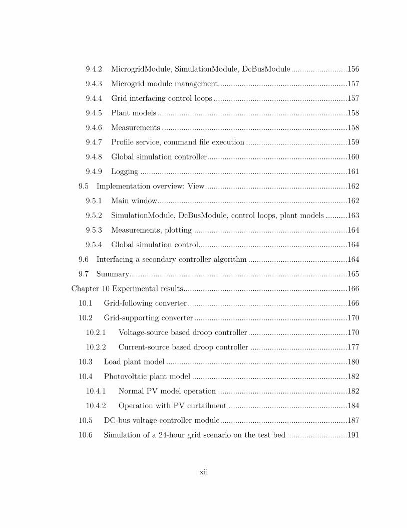
2.3.2 Grid-feeding / grid-following converters2
A grid-feeding converter can be modeled as a current source with a parallel impedance
connected to an AC Microgrid bus, as depicted in Figure 2.7. A controller controls active
and reactive power injection into this bus based on local measurements of injected cur-
rent, bus voltage level and bus frequency. The role of this converter representation is to
inject a predetermined amount of active and reactive power into the local bus, without
active participation in voltage or frequency control. For example, this is commonly used
2 The terms “grid-feeding converter” and “grid-following converter” are used interchangeably in this
thesis.
Chapter 2
Background review
20
with non-dispatchable generation, such as photovoltaic plants or wind turbines, which
controls the conversion of primary energy using maximum power point trackers (MPPT).
Grid-feeding converters are not able to form and sustain a Microgrid by themselves.
Instead, they are reliant on the existence of a voltage source based converter in the grid.
The measurement of the bus frequency is commonly performed using a phase-locked
loop (PLL) [29].
Figure 2.7 Grid-feeding controller representation
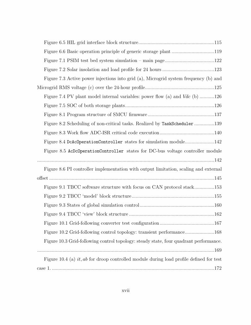
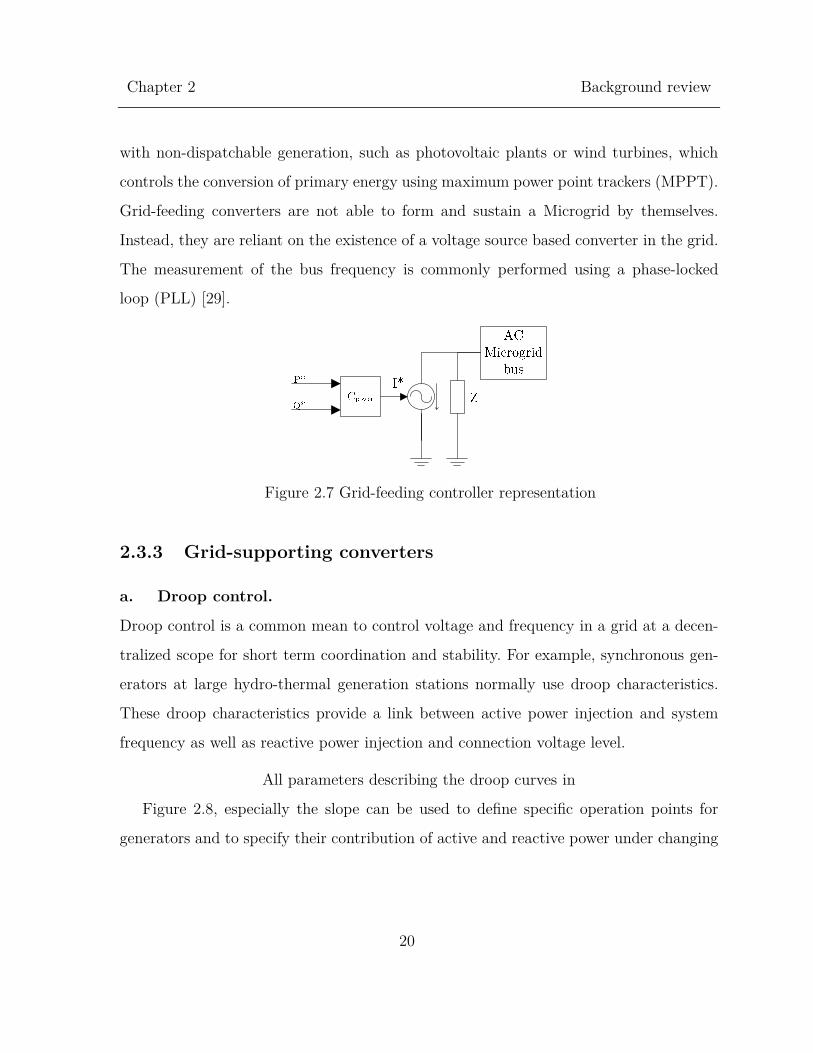
2.3.3 Grid-supporting converters
a. Droop control.
Droop control is a common mean to control voltage and frequency in a grid at a decen-
tralized scope for short term coordination and stability. For example, synchronous gen-
erators at large hydro-thermal generation stations normally use droop characteristics.
These droop characteristics provide a link between active power injection and system
frequency as well as reactive power injection and connection voltage level.
All parameters describing the droop curves in
Figure 2.8, especially the slope can be used to define specific operation points for
generators and to specify their contribution of active and reactive power under changing

Chapter 2
Background review
21
grid conditions. This concept has been adapted for power converters and is discussed in
more detail in section 2.7.
Figure 2.8 Droop curves for P/f and Q/V droop
b. Grid-supporting converters
The grid-supporting converter is among the most investigated controller topology types
in recent literature on primary control of Microgrids [30]–[35], since it is a tool to provide
the services required by the primary and secondary control layers of Microgrids by means
of droop control [3].
Grid-supporting converters support a grid-forming converter and, in certain circum-
stances, can replace it. Grid-supporting converters are an extension to the representation
of a grid-former (Figure 2.10) or a grid-feeder (Figure 2.9), respectively. The goal of grid-
supporting converters is to regulate the PCC voltage and frequency close to desired
values to support or replace the operation of a grid-former. A voltage-source based droop
controller is able to form an islanded grid, while a current-source based droop controller
relies on an existing grid to synchronize to, since it uses a PLL to determine the current
grid angle and frequency instead of setting it.
Chapter 2
Background review
22
Figure 2.9 Current-source based droop controller representation
Figure 2.10 Voltage-source based droop controller representation
The following sections will introduce concepts that are needed to implement the con-
troller representations mentioned in section 2.3. Controller implementations itself are
presented in Chapter 5.
2.4 Control in the synchronous reference frame
2.4.1 The abc-dq0 transformation
A very established controller concept is the proportional-integral controller (PI control-
ler) because of its simplicity. For DC quantities it offers infinite gain and thus zero
steady-state error. Its transfer function in parallel block representation is:

Chapter 2
Background review
23
ᵃ���(ᵅ�) = ᵅ�� + ᵅ��ᵅ�
(2.4)
Since most quantities in power converters for AC Microgrids (converter duty cycles,
connection voltage, injected currents, etc.) are dominantly AC with a frequency of 50Hz
or 60Hz, PI controllers cannot offer zero steady-state error when directly applied to the
AC waveforms. To overcome this problem, a common solution is to transform these AC
quantities to a synchronous reference frame first. This transforms all components of a
desired frequency (50Hz or 60Hz, for example) to DC quantities. For these DC quanti-
ties, a PI controller will show zero steady-state error.
Transformation to a synchronous reference frame is performed by Park’s transfor-
mation [36] and a slightly altered abc-dq0 transformation [37]. Park’s transformation is
magnitude-invariant while the other abc-dq0 transformation is power-invariant. For the
purpose of this thesis, park’s abc-dq0 and dq0-abc formulations given by equations (2.5)
and (2.6) are used.
ᵃ���� = 23
⎣⎢⎢⎢⎢⎡ cos (ᵰ�) cos �ᵰ� − 2ᵰ�
3� cos �ᵰ� + 2ᵰ�
3�
−sin (ᵰ�) − sin �ᵰ� − 2ᵰ�3
� − sin �ᵰ� + 2ᵰ�3
�
12
12
12 ⎦
⎥⎥⎥⎥⎤
(2.5)
ᵃ����−� =
⎣⎢⎢⎢⎡
cos (ᵰ�) − sin(ᵰ�) 1
cos �ᵰ� − 2ᵰ�3
� − sin �ᵰ� − 2ᵰ�3
� 1
cos �ᵰ� + 2ᵰ�3
� − sin �ᵰ� + 2ᵰ�3
� 1⎦⎥⎥⎥⎤
(2.6)

Chapter 2
Background review
24
2.4.2 The dq0 controller block
In order to control AC quantities of a power converter using PI controllers, all relevant
measurements, such as output voltages and currents, can be transformed to a synchro-
nous reference frame using equation (2.5). When using the correct reference angle ᵰ� at
correct angular speed ᵱ�, these measured values will become DC quantities for the desired
frequency values (ᵱ�) at which a PI controller will yield zero-steady state error. This
basic setup is represented by the blocks lining up to the right of the signals d* and q*
in Figure 2.11.
For the zero channel, no PI controller is presented because for this thesis there has been
no need to control zero channel values. This is especially true since the Δ-Y transformers
used in the final configuration of this Microgrid test bed prevent the existence of a zero
component.
The universal dq0 controller block that is used in grid interface controller topologies in
this Microgrid test bed is shown below.
Figure 2.11 dq0 controller block structure

Chapter 2
Background review
25
2.4.3 Decoupling of d and q channels
The three-phase LCL filter of Figure 2.12 is a filter structure commonly used for three-
phase grid-connected converters. The state equations describing this filter are [31]:
ᵃ��ᵃ�ᵅ���ᵃ�ᵅ�
= ᵆ��ᵴ�ᵆ��� + ᵅ��� − ᵅ���
ᵃ��ᵃ�ᵅ���ᵃ�ᵅ�
= −ᵆ��ᵴ�ᵆ��� + ᵅ��� − ᵅ���
ᵃ��ᵃ�ᵅ���ᵃ�ᵅ�
= ᵆ��ᵴ�ᵆ��� + ᵅ��� − ᵅ���
ᵃ��ᵃ�ᵅ���
ᵃ�ᵅ�= −ᵆ��ᵴ�ᵆ��� + ᵅ��� − ᵅ���
ᵃ��ᵃ�ᵅ���ᵃ�ᵅ�
= ᵆ��ᵴ�ᵆ��� + ᵅ��� − ᵅ���
ᵃ��ᵃ�ᵅ���ᵃ�ᵅ�
= −ᵆ��ᵴ�ᵆ��� + ᵅ��� − ᵅ���
(2.7)
(2.8)
(2.9)
(2.10)
(2.11)
(2.12)
Figure 2.12 Single phase representation of a converter output LCL filter
The bold parts in equations (2.7)-(2.12) represent couplings between the d and q
channels, since for a d-channel state equation a term from the q channel appears and

Chapter 2
Background review
26
vice versa. Decoupling terms in controllers for synchronous reference frames are com-
monly added to the controller output to offset this channel coupling. This is apparent
in Figure 2.11 where G stands for ᵃ�� , ᵃ�� or ᵃ��, respectively, in equations (2.7)-(2.12).
2.4.4 Feed-forward terms
In order to improve the converters performance under transient conditions of the con-
nected grid, feed-forward terms can be introduced to the controllers’ outputs. Feed-
forward terms take away the need of a controller to provide an output that adjusts to
an indirectly dependent parameter that can be measured. For a controller that controls
the current flow through the filter inductors ᵃ�� , the role of feed-forward terms can be
described as follows.
Given equations (2.7) and (2.8), the change of current in the filter inductors is a
function of ᵅ���, ᵅ��� and ᵅ���, ᵅ��� (neglecting ᵃ��ᵱ� × ᵅ��� and −ᵃ��ᵱ� × ᵅ��� that are irrele-
vant due to decoupling terms). The means of a current controller to control ᵅ��� and ᵅ���
are adjusting ᵅ��� and ᵅ���, respectively. Values of ᵅ��� and ᵅ��� are dependent on ᵅ���, ᵅ���
and the current flow towards the AC Microgrid bus. By adding ᵅ��� and ᵅ��� to the con-
trollers output the PI controller does not have to react to changes in these variables in
order to maintain the desired current flow. A feed-forward gain ᵃ� (ᵃ� = 0 …1) allows to
scale the effect of feed-forward terms.
2.4.5 Controller output limiting
The output of some controllers must be limited to a definable range. Reasons for this
include protection, energy limitations within the simulated plant, plant sizing and other
hardware requirements:

Chapter 2
Background review
27
1. Protection. The hardware design of an inverter assumes a certain value for
maximum steady state currents. Continuous operation beyond these values
could damage the system. For example, it could overheat filter inductors or
transformers. However, the system is capable of handling short term transients
in excess of these thresholds so that an immediate system shut down is not
required.
2. Simulated plant. HIL simulation of plants may result in certain limitations
of power injected into or withdrawn from the AC bus. For example, this can be
necessary when the availability of primary energy is below the actual plant size
from time to time.
3. Plant sizing. This test bed is supposed to represent a real system when scaled
down. To represent different relative sizing of plants, it must be possible to
limit output power according to artificially-set power limits.
4. Other hardware requirements. The PWM duty cycles generated for the
PWM gate signal generation system will determine the mode of operation of
the inverter (linear PWM, overmodulation or square-wave mode of operation).
To provide capabilities of selecting specific modes, limitation of PWM duty
cycles is desirable. This ensures that square-wave mode of operation does not
occur in any transient situation.
Active power, reactive power or complex power limits can be required and have to be
applied separately for maximum and minimum limits. Discussions of possible control
loop topologies in the synchronous reference frame in subsequent sections show that it
is often possible to represent active power flow in the d channel and reactive power flow
in the q channel. Since ᵃ� = �ᵃ�� + ᵃ��, complex power can be limited by limiting
Chapter 2
Background review
28
�ᵅ�ᵅ�ᵅ��� + ᵅ�ᵅ�ᵅ��� to a pre-specified value. ᵅ�ᵅ�ᵅ�� and ᵅ�ᵅ�ᵅ�� refer to the d and q channel output
before complex power limitation, respectively. These complex channel limits (ᵅ�ᵅ�ᵅ�ᵅ���� <
�ᵅ�ᵅ�ᵅ��� + ᵅ�ᵅ�ᵅ��� < ᵅ�ᵅ�ᵅ�ᵅ�ᵅ����) can be translated into d and q channel limits as outlined in
Code listing 1 in appendix C.1. Such a transformation has to be computed at every
control loop execution.
An implementation of d and q channel limits has to include possible contributions to
ᵅ�ᵅ�ᵅ�� and ᵅ�ᵅ�ᵅ�� from feed-forward terms, decoupling terms and output scaling ᵅ�. Anti-
windup schemes and/or dynamic curtailment of the integral controller part have to be
adapted to this case.
Applying a constant limit to d and/or q channel with synchronous reference frame
controller topologies will not introduce additional harmonics into the system in most
cases. This is advantageous over stationary frame controller topologies where a simple
limiting using constant values of a sinusoidal waveform results in a heavily distorted
waveform. Separation of active and reactive power limits is also not as simple to achieve
in the stationary reference frame case.
2.5 Control in the stationary reference frame
The abc-dq0 transformation and its inverse are computationally intensive due to many
trigonometric functions involved. The computational overhead becomes significant when
using fixed-point, low-cost microcontrollers and applying advanced concepts that require
multiple transformation pairs. Such advanced concepts can be negative sequence voltage
control / unbalanced loading control or harmonic compensation. To overcome these lim-
itations, the concept of proportional + resonant (PR) controllers has been developed

Chapter 2
Background review
29
[38]. These controllers are characterized by a proportional gain and a system that reso-
nates at one desired frequency, typically 50Hz or 60Hz, thus providing infinite gain at
this frequency. PR controllers are typically used in the ᵯ�ᵯ� stationary reference frame for
three-phase VSI inverters. It has been shown that a PR controller using a controller
transfer function as given in equation (2.13) is mathematically equivalent to a synchro-
nous reference frame PI controller implementation [39]. By adding paralleled PR con-
trollers tuned to selected harmonic frequencies (3ᵃ��, 5ᵃ��, 7ᵃ��, etc.; ᵃ�� being the funda-
mental frequency) it is possible to achieve harmonic compensation at low cost. A more
commonly implemented transfer function is equation (2.14) due to computational issues
and to provide a wider controller bandwidth in case of grid frequency variations. This
equation involves a damping term ᵱ�� that limits the controller gain to a finite value,
introducing a small steady-state error. Several issues surrounding numerical stability of
digital implementations have been addressed in [39], [40]. However, a computationally
fast and reliable method to limit the output of PR controllers without introducing ad-
ditional harmonics into the system, and to specifically limit active, reactive and complex
power is currently not available.
Since this project builds on a floating-point processor with extensions for fast trigono-
metric function computation, and due to insufficient limiting capabilities of PR control-
lers, this project mostly focuses on control in the synchronous reference frame using the
dq0 controller block structure.
ᵃ������(ᵅ�) = ᵃ�� + 2ᵃ��ᵅ�ᵅ�� + ᵱ�� (2.13)
ᵃ����−�����(ᵅ�) = ᵃ�� + 2ᵃ��ᵱ��ᵅ�ᵅ�� + 2ᵱ��ᵅ� + ᵱ�� (2.14)

Chapter 2
Background review
30
2.6 Phase-locked loops for grid application
For some converter roles it is necessary to extract the current angle Θ of the sinusoidal
grid voltage. This angle Θ can then be used as reference angle for abc-dq0 transfor-
mations or as angle for reference value generation, if control is performed in the natural
or stationary reference frame. Various PLL approaches are known and have been widely
discussed in literature [29], [41]–[44], such as the synchronous reference frame PLL (SRF
PLL), decoupled double synchronous reference frame PLL (DDSRF PLL), and the dual
second order general integrator PLL (DSOGI PLL). Due to its simplicity, this thesis
focuses on the SRF PLL which has proven to be satisfactory under balanced voltage
conditions for three-phase systems [41]. For unbalanced and distorted grid conditions a
more complex PLL structure might become desirable.
For three-phase applications an SRF PLL (adapted from [42]) as depicted in Figure
2.13 can provide grid angle Θ and grid frequency ω. The PLL performance mostly de-
pends on the tuning of the integrated PI controller. A frequency bias of 2ᵰ�60 rad/s
provides a fast convergence at execution start-up.
Figure 2.13 Three-phase synchronous reference frame PLL structure
In some cases only one of three voltage signals is available or the grid voltage angle
in a single-phase system is to be determined. For this case the three-phase SRF PLL can
be adapted using a transport delay and the ᵯ�ᵯ�-dq0 transformation instead of an abc-

Chapter 2
Background review
31
dq0 transformation. This approach is adapted from [44] and given in Figure 2.14. To
determine the phase angle of a single sinusoidal voltage ᵅ��, it is interpreted as a signal
for the α channel of an αβ-dq0 transformation. Under undisturbed conditions, the beta
channel signal is supposed to be a sinusoidal function of similar shape delayed by 90
degree. This is realized using a transport-delay.
Figure 2.14 Single-phase synchronous reference frame PLL structure
2.7 Voltage-source based droop control
2.7.1 Droop control for grid-supporting converters
Traditional, machine-dominated grid control using P/f and Q/V droop behavior has
been adapted in the control of power electronic converters for grid applications. The
basic formulation of these droop relationships can either be solved for frequency and
voltage or for active and reactive power. Voltage-source based droop controllers require
a reference voltage and a reference angle. Therefore, for these controllers the basic droop
equations are [29]:
ᵃ�∗ = ᵃ�� − ᵅ��(ᵃ� − ᵃ��) (2.15)
ᵃ� ∗ = ᵃ�� − ᵅ��(ᵃ� − ᵃ��) (2.16)

Chapter 2
Background review
32
These equations can be used in a droop controller for this converter role where the
assumed cascaded controller structure is as given in Figure 2.15 (after [31]).
Figure 2.15 General controller structure for voltage-source based droop controlled
converters
However, it has been shown that the stability of this droop control for power electronic
converters is dependent on the operating point; in fact the system’s eigenvalues approach
the imaginary axis when output active and reactive power is increased [32]. To improve
the droop stability one proposed solution is to introduce derivative terms into the droop
equations and schedule the derivative gains based on the current operating point (equa-
tions (2.17) and (2.18)) [32]. This publication shows that the droop controller dynamics
can be fixed to a certain eigenvalue using gain scheduling, if system parameters of the
connection impedance are known. However, it also demonstrates that the variation of
scheduled gains is relatively small for a wide range of operation for the example case,
which can lead to the assumption that constant derivative gains can provide significant
performance improvements for many cases. Further investigation would be required.
ᵃ�∗ = ᵃ�� − ᵅ��(ᵃ� − ᵃ��) − ᵅ���ᵃ�ᵃ�ᵃ�ᵅ�
(2.17)
ᵃ� ∗ = ᵃ�� − ᵅ��(ᵃ� − ᵃ��) − ᵅ���ᵃ�ᵃ�ᵃ�ᵅ�
(2.18)

Chapter 2
Background review
33
2.7.2 Virtual impedance
Traditional droop control has been implemented with transmission grids in mind which
are dominantly inductive. As presented in the previous section, droop control adapted
for power electronic converters follows the same assumption. However, in distribution
grids this assumption does not always hold as the X/R ratio is commonly smaller. In
order to provide more design flexibility for the connection impedance seen by a DG
inverter, the concept of virtual impedance has been developed [4], [45]. Additional to the
real existing connection impedance ᵃ�� with a given X/R ratio, an additional virtual
connection impedance ᵃ�� can be incorporated into the converter control (see Figure
2.16). This concept offers the ability to modify the connection impedance seen by an
inverter to any desired value without additional losses or space requirements. Any posi-
tive or negative inductive or resistive impedances can be added.
Figure 2.16 Virtual impedance ᵃ��
This concept is realized through modification of controller set points depending on the
injected current ᵅ������.
For voltage-source based droop controllers the voltage reference ᵃ� ∗ can be altered in
order to simulate a voltage drop across a virtual impedance. In the dq0 reference frame
this can be calculated as:
Chapter 2
Background review
34
ᵅ��� =
√2ᵃ�� + ᵱ�ᵃ�� i�� −ᵃ��ᵅ���
ᵅ��� = −ᵱ�ᵃ�� i�� −ᵃ��ᵅ��� (2.19)
For current-source based droop controllers a modified power reference can be derived
from the initial reference in order to mimic a steady-state power consumption by a
virtual impedance:
ᵃ���= ᵃ��ᵃ��
� = ᵃ�� � ᵃ�∗
32 ᵅ���ᵅ���
√2�
�
ᵃ���= ᵱ�ᵃ��ᵃ��
� = ᵱ�ᵃ�� � ᵃ�∗
−32 ᵅ���ᵅ���
√2�
�
(2.20)
Derivations of equations (2.19) and (2.20) are presented in the appendices A.1 and A.2.
Using this concept, the connection impedance seen by the inverter’s droop control can
be altered in order to ensure a good performance of given droop controllers. Additionally,
virtual impedance can be used during grid synchronization. In this case a high initial
virtual impedance that is reduced over time can facilitate a gradual synchronization
without overloading the inverter.
2.7.3 Power droop decoupling due to X/R ratio
As stated before, traditional droop mechanisms assume a very high X/R ratio of the
grid connection impedance and the grid impedances itself. If this is the case, an active
power-frequency droop (P/f droop) is without coupling to a reactive power-voltage droop
(Q/V droop). However, if the impedances of a network have a lower X/R ratio, as com-
mon in distribution grids, a change in active power injection will also lead to a change
of system voltage and a change in reactive power will also lead to a change in the
connection impedance’s voltage angle. Then, there is a coupling between P/f and Q/V

Chapter 2
Background review
35
droops which degrade the droop controller performance, especially for voltage-source
based droop controllers [30]. In order to decouple these droops, [30] proposes a transfor-
mation matrix based on the X/R ratio:
�ᵃ��
ᵃ�′� = ᵃ� �ᵃ�ᵃ�� =
⎣⎢⎢⎡
ᵃ�ᵃ�
−ᵃ�ᵃ�
ᵃ�ᵃ�
ᵃ�ᵃ� ⎦
⎥⎥⎤
�ᵃ�ᵃ�� =
⎣⎢⎢⎡
ᵅ�√ᵅ�� + 1
− 1√ᵅ�� + 1
1√ᵅ�� + 1
ᵅ�√ᵅ�� + 1 ⎦
⎥⎥⎤
�ᵃ�ᵃ�� (2.21)
where ᵅ� = ��. The droop equations are then based on ᵃ�� and ᵃ�� instead of the measured
ᵃ� and ᵃ�.
This transformation will not change the fact that upon a frequency change, active and
reactive power injection will change; however, the droop controllers will not see this
coupling and therefore show an improved convergence behavior. However, this can only
be achieved, if a good estimate of the X/R ratio is available. In comparison to the virtual
impedance concept, this approach does not try to alter the connection impedance, but
rather tries to adjust droop control to a given impedance.
2.7.4 Negative sequence control
If a voltage-source based droop controller feeds unbalanced loads with a voltage control-
ler in the synchronous references frame for balanced operation, a voltage unbalance be-
comes apparent. This unbalance can be represented by a desired positive sequence volt-
age and an unwanted negative sequence component. Therefore, it is desirable to control
the negative sequence voltage component at the inverter filter capacitor to zero.

Chapter 2
Background review
36
In order to achieve this, the voltage control structure of a synchronous reference frame
controller can be duplicated and paralleled. One structure remains as configured to con-
trol the amplitude of the desired positive sequence voltage. A second structure aims to
control the negative sequence component to zero.
When applying the abc-dq0 transformation on the filter capacitor voltages with – ᵱ�
(where ᵱ� is the grid frequency), all negative sequence components will become constant
values. As PI controllers offer zero steady-state error for constant values only, this con-
cept can be used to regulate negative sequence filter capacitor voltages to zero. This can
only be done through supplying the unbalanced load currents requested which will be
the controller action taken to achieve the control objective.
[46] introduces this principle. It also shows that the voltage references for a negative
sequence voltage controller have to be:
ᵅ�����
∗ = ᵃ�� cos(2ᵰ�)
ᵅ�����∗ = −ᵃ�� sin(2ᵰ�)
(2.22)
where ᵃ�� is the desired positive sequence voltage amplitude that is used as reference
to ᵅ�����∗ (ᵅ�����
∗ = 0). This principle is used in the implementation of the voltage-source
based droop controller in this thesis and is depicted in more details in Chapter 5.

Chapter 2
Background review
37
2.8 Control of direct parallel connected 3-phase in-
verters
2.8.1 Using ᵪ�ᵆ� transformers
The traditional solution to connection of three-phase VSIs to electricity grids is using
Δᵃ� transformers. Figure 2.17 shows two of such converters connected in parallel on both
AC and DC sides (“direct parallel connection”).
Figure 2.17 Two direct parallel connected 3-phase VSIs using Δᵃ� transformers
There are several advantages using a Δᵃ� transformer in single or multi converter con-
figurations:
Isolation. Isolation between the inverter and grid can provide flexibility in
grounding and protection. It also removes any common-mode voltage noise that
pulse-width or space-vector modulation might introduce into the AC bus at
multiples of the switching frequency [47].

Chapter 2
Background review
38
No zero sequence current transfer. Due to the Δ connections on the in-
verter side, zero sequence currents (ZSC) cannot flow. This makes any control
of ZSC unnecessary and simplifies inverter control. In this thesis, a converter
structure is proposed that involves direct parallel converter connection. If no
Δᵃ� transformer breaks the ZSC path, these currents can circulate freely
through AC and DC sides of the inverters.
Neutral wire provision. Due to the ᵃ� connection on the grid side, a neutral
wire can be provided without implementing it on the inverter side. This reduces
the number of inverter legs and filter components required and also reduces
control complexity.
Voltage boost. If the connection voltage level is at medium or high-voltage it
can be desirable to provide a voltage boost by a transformer so that the inverter
can be implemented at lower output voltage levels.
However, transformers also introduce significant disadvantages into a grid connected
inverter system. Main disadvantages are:
Cost. As transformer windings are made out of copper, their cost is a signifi-
cant share of an inverter system total cost. For example, 5kVA transformers for
this thesis project have been quoted at around CAD$ 800. The total material
cost of an inverter system has been estimated at CAD$ 2000-3000, initially. A
detailed analysis of the realized system follows in section 4.6.
Size and weight. A 5kVA transformer for this application weigh around 60-
70kg making them the heaviest single component in the inverter system. The
same applies to the size.

Chapter 2
Background review
39
Losses. Transformers have conduction and core losses that reduce the inverter
systems efficiency.
Magnetization currents. Transformers consume reactive power in order to
magnetize the core. This can cause issues at grid connection, inverter sizing
and in inverter control. In addition, the magnetization currents of the three
phases for the transformers used in this thesis were unbalanced, so that inverter
control has to address this in order to maintain a balanced connection voltage
level.
Current harmonics. Due to the core design of common transformers, signif-
icant harmonics exist in magnetization currents. This has influence on inverter
control and power quality.
2.8.2 Using four converter legs and zero sequence current control
As an effort to overcome aforementioned disadvantages with transformer-based solutions,
methods have been investigated to allow for a transformer-less direct parallel operation.
Replacing Δᵃ� transformers with filter inductors introduces issues in isolation, ground-
ing, waveform quality and control that have to be addressed in order to successfully
implement a transformer-less solution into the test bed.
Figure 2.18 shows a general structure for two four-leg VSIs where the fourth leg pro-
vides the neutral wire to the AC Microgrid bus.

Chapter 2
Background review
40
Figure 2.18 Two direct parallel connected 3-phase VSIs with four legs and not
transformer
With such a setup, the disadvantages of cost, size and weight, losses, magnetization
currents and current harmonics of a transformer-based configuration can be fully or
partially overcome. However, other disadvantages are introduced into the system that
partially apply to all cases and partially are specific to the chosen solution.
a. Controlling ZSC with pulse-width modulation
In order to control the flow of ZSC between two inverters [48] suggests splitting each
of the PWM duty cycles ᵃ��, ᵃ�� and ᵃ�� into two parts:
ᵃ�� = ᵃ��� + ᵃ��
� (2.23)
ᵃ�� = ᵃ��� + ᵃ��
� (2.24)
ᵃ�� = ᵃ��� + ᵃ��
� (2.25)
Furthermore, ᵃ�� = ᵃ��� .

Chapter 2
Background review
41
Then, ᵃ��� can be used by a PI controller to control the ZSC flowing in or out of one
inverter since it changes the average common voltage level of all inverter legs compared
to those of another inverter. ᵃ��� , ᵃ��
� and ᵃ��� serve as duty cycles to produce sinusoidal
waveforms. This approach is a simple and effective approach to keep ZSC currents close
to zero. Hardware support by common microcontrollers is very good for pulse-width
modulation so that this approach can easily be integrated. However, the system has to
be designed in a way that reduces the maximum values for ᵃ��� , ᵃ��
� and ᵃ��� so that an
additional ᵃ��� values does not force the inverter out of a linear modulation range.
b. Controlling ZSC with space vector modulation
In [49] it is proposed that the zero vector in an SVM is split into two vectors. One
vector has a low instantaneous common leg voltage, the other a high as depicted in
Figure 2.19. A parameter ᵅ� allows to alter the ratio of average high and average low
common leg voltages which then allows to increase or decrease the ZSC level of one
inverter. This is the necessary tool to control ZSC current to zero using a control loop,
for example, in the zero channel of a dq0 control block. It has to be noted that with this
method the converter has to be designed in such a way that at peak values the active
vectors do no use up all the available time in an SVM switching cycle, so that significant
control margin for the ZSC controller is still available. This effectively means to increase
ᵃ��� or to decrease ᵃ��̂�����. Also, implementation of an SVM in microcontroller is not
supported by hardware, so far. This means that all SVM implementations have to be
done in software which adds significant computational constraints to these controllers.

Chapter 2
Background review
42
Figure 2.19 ZSC current control based on modified SVM. Depicted: Instantaneous
leg voltages between ᵃ��� and ground for one switching cycle in a three-leg inverter.
c. Reduction of common-mode voltage noise
With traditional PWM the common-mode voltage ᵃ��� (Figure 2.18) changes from min-
imum to maximum DC-bus voltage at the switching rate (see Figure 2.20). If two un-
synchronized inverters are operated in parallel with this scheme, common-mode voltage
drops across the filter inductances between all involved inverters will cause high fre-
quency ZSC ripples between these inverters. These high frequency ripples will increase
losses in inverter switches and filter inductors. Also, the sizing of filter inductors and
requirements on the maximum RMS ratings are influenced by the presence of these
ripples.
Figure 2.20 ᵃ��� for traditional PWM for a single inverter

Chapter 2
Background review
43
For PWM inverters, it can be shown that operating under PWM regime, when carrier
signals for control of inverter legs A, B and C are phase shifted by ± 120° with respect
to one another, can reduce the high-frequency common-mode voltages as long as the
modulation index is below ᵅ��� = �� (a fourth leg is neglected in this case).
Elimination of high-frequency common-mode voltage noise can be achieved with a
four-leg inverter as demonstrated in [50]. However, this method does not provide the
necessary degree of freedom to control low-frequency zero sequence current that could
occur from system imbalances local ᵃ��� variations or other transient effects.
For multi-level inverters, which are not considered for this thesis project, multiple
approaches exist to reduce or eliminate high-frequency common-mode voltage noise with
different trade-offs (for example: [51]–[54]).
d. Assessment of transformer-less methods for direct parallel connected
inverters
Compared to Δᵃ� transformer based scenarios, using a structure without such a trans-
former yields some advantages:
Lower cost, size and weight. A transformer is not necessary any more.
However, the following additional components have to be added: an inverter
leg, two switch drivers and corresponding power supplies, filter components and
sensors.
No magnetization currents.
Potentially lower level of inductor core saturation. Due to more design
freedoms.

Chapter 2
Background review
44
However these methods also come with significant limitations and disadvantages: Higher control complexity. Modulation scheme and control loops have to
be adapted and waveform quality is affected in most scenarios.
Increased THD. High-frequency, common-mode voltage noise increases the
noise floor in the system, thus worsens the total harmonic distortion (THD) of
output waveforms.
More complicated LCL filter design. High frequency common-mode noise
adds constraints onto the inductor design and as a consequence can slow down
control loop dynamics.
Less flexible grounding. Depending on the chosen modulation scheme, the
average value for ᵃ��� is at ���� or close to this value. Since there is no isolation
transformer, this voltage level is also present at the AC Microgrid bus that has
to be able to deal with it. Grounding, EMI design and protection has to take
this into account.
Less efficient modulation range usage. For common-mode voltage reduc-
tion schemes, a higher DC-bus voltage is required leading to an oversizing of
components.
In order to keep the control loop complexity low, allow for a more flexible set of
components connected to the AC Microgrid in the future (especially electric machines)
and maintain a low THD in the Microgrid voltages this thesis focuses on inverters con-
nected in parallel using Δᵃ� transformers. However, it should be emphasized that both
solutions are feasible. A hardware-based comparison in this test bed can be of great
interest as future work. Therefore this test bed takes specific requirements of trans-
former-less designs into account with respect to the overall system structure design to

Chapter 2
Background review
45
give room for future expansions. This includes providing sensor and PWM connections
for a fourth leg to the microcontroller and allowing an increase in the DC-bus voltage,
if required.

Chapter 3
Test bed system structure design
46
Chapter 3
Test bed system structure design
3.1 System component arrangement
Based on the goal definition in section 1.4 the overall system structure shown in Figure
3.1 is proposed in this thesis.
Figure 3.1 Overall Microgrid test bed structure

Chapter 3
Test bed system structure design
47
Subsequently, all major components of this structure are described.
1. Simulation module. A simulation module consists of a power electronic con-
verter that converts DC power to AC power and controls output voltage, current,
power and/or frequency on the AC side. This converter includes all necessary
sensors, filters and protection equipment, as well as processor(s) to provide
enough computational capacity. Its firmware allows reconfiguration of a simula-
tion module at runtime to change its behavior on the AC bus side to any desired
generator or load characteristic available. This system allows parallelization of a
large number of simulation modules. Simulation modules reproduce desired simu-
lation behavior (of a certain generation plant or load) on their AC side only.
2. DC-bus voltage controller. The “DC-bus voltage controller” is a module de-
rived from the simulation module. Its task is to provide a stable and sufficiently
high DC-bus voltage of good quality for all simulation modules. This is the only
module that connects to the electricity grid available in the laboratory.
3. AC Microgrid bus. As this test bed focuses on the simulation of isolated Mi-
crogrids, a grid connection is not necessary at this point. Therefore, this bus is a
four wire stand-alone bus. Network impedances, switchgear, LTCs, similar distri-
bution grid equipment and different voltage levels (LV, MV…) are neglected in
this thesis as a simplification.
4. Simulation Controller. One central software allows to set all parameters that
define the environment in which this Microgrid simulation is performed, in order
to replicate real-life conditions. Such parameter setting can include component
sizing, control loop selection and configuration, plant selection and configuration,

Chapter 3
Test bed system structure design
48
weather data or load demand curves, for example. Furthermore, it allows to rec-
ord measurement data that is available to simulation modules through their sen-
sor readings. There is only one simulation controller in this test bed.
5. Microgrid Controller. Another piece of software allows to run any Microgrid
central control algorithms. This can be a controller for secondary and/or tertiary
control levels, for example. Microgrid Controller and Simulation Controller are
two components in the same software, called Test bed central controller (TBCC).
6. Communication link. A communication link connects all active elements in
the test bed. This link provides communication capabilities for all data exchange
required by simulation controller and Microgrid controller. Additionally, it allows
direct communication between simulation modules for protection coordination
and in case any decentralized Microgrid control algorithms (such as Multi-Agent
systems, for example [55], [3]) require communication to neighboring modules.
In this system, the DC-bus does not represent any simulated quantity. Instead, it pro-
vides a connection between all modules to let the energy handles by other simulation
modules. The DC-bus voltage is controlled to be constant at all times during operation.
An advantage of this approach compared to many other Microgrid test beds is that the
amount of energy needed for a simulation is far below the energy circulated in the Mi-
crogrid. Only losses in the system (such as switching losses) need to be compensated for;
all other energy is circulated in the system.

Chapter 3
Test bed system structure design
49
3.1.1 System component sizing
a. Power rating
In order to proceed with more detailed hardware design, specifications on target system
component sizing have to be defined. As mentioned in the goal definition, the desired
power rating for simulation modules on their AC side is 5kVA. This power rating is
chosen, so that this test bed can easily be operated in the laboratory available to this
research group.
Standard three-phase power available is 208VLL, 60Hz, 20A. This is equivalent to
7.2kVA. Certain space and weight restrictions apply that discourage the use of AC trans-
formers with higher power ratings that have a significantly higher weights. At the same
time, using a power rating of up to 5kVA allows to perform almost full-scale simulations
for small DG plants, such as residential photovoltaic stations. It is also high enough so
that components from categories commonly used in real power products can be used.
This is especially true for the IGBT switches, filter components and distribution trans-
formers, so that their specific advantages and disadvantages become apparent.
The DC-bus voltage controller module is derived from a simulation module. Assuming
a simulation module converter efficiency of 90% at full load, each simulation module will
require the compensation of 500W on the DC-bus. If the DC-bus voltage controller
module is also sized for 5kVA it can supply nine to ten simulation modules at full load.
This is considered sufficient for the scope of this thesis and the near foreseeable future.

Chapter 3
Test bed system structure design
50
3.1.2 AC Microgrid voltage
Using standard voltages increases compatibility with potential extensions of this Mi-
crogrid with external components, brings test results closer to real cases and allows the
selection of standard components available on the market.
For this reason, an AC Microgrid voltage of 120ᵃ���/208ᵃ��� is chosen which results
in a maximum simulation module AC current of 13.89Arms at full load. Any higher volt-
age level results in very low currents, but equipment for higher voltages is typically used
in applications with higher power levels than 5kVA.
3.1.3 DC-bus voltage
For three-phase voltage source inverters the following relationship between AC and DC
voltages exists [25]:
ᵃ��̂�� = ᵅ��ᵃ���2
(3.1)
where ᵃ����� is the peak value of the fundamental component of the phase-to-neutral
voltage. Consequently, the minimum DC voltage required to produce a sinusoidal output
voltage (line-to-neutral) ᵃ��(RMS) is (ᵅ�� = 1):
ᵃ������� = 2√
2ᵃ�� (3.2)
The maximum required steady-state value for ᵃ�� is dependent on the system voltage,
filter component size and maximum power rating. Assuming a VSI with an LCL filter,

Chapter 3
Test bed system structure design
51
filter inductors of size 1.5mH and filter capacitors of size 50μF values and an AC Mi-
crogrid voltage amplitude of 126V3 the maximum inverter voltage magnitude ᵃ�� is
139.5V. Please refer to appendix A.3 on page 204 for a derivation.
According to equation (3.2) the minimum DC-bus voltage becomes: 394.6V. In order
to provide controllers with some more margin for harmonics, unbalances, noise and tran-
sients before leaving the linear mode of operation, a DC-bus voltage of 450V has been
chosen. This results in a maximum expected modulation index ᵅ������ = ���������� = 0.88.
If there are extensions to the test bed that require a maximum modulation index ᵅ�� of ��, for example, to reduce common mode voltage noise in direct parallel connected three-
phase, four-leg VSIs, then the DC-bus voltage should be raised to about 600V. This will
have implications on applied protection measures.
3.1.4 Communication link
The purpose of the communication link is to enable system configuration, coordination
and measurement transmission. High-speed system control loops in Microgrids are com-
monly not implemented across communication links to avoid limiting reliability due to
limitations of the communication link reliability [3]. Therefore the requirements on this
communication link are:
Simple command transmission. For example, a bus structure as network topol-
ogy does not require packet routing compared to a star, tree or hybrid network
arrangements common with standards such as Ethernet.
3 Upper value of common distribution grid voltages, ANSI C84.1.

Chapter 3
Test bed system structure design
52
Easy and computationally fast to implement in a target microcontroller plat-
form
Medium average data transfer rate for measurement data transfer in real-time
No special requirements on delay or jitter
Robust electrical design regarding EMI
Out of the communication interfaces that are commonly available on considered mi-
crocontroller platforms, the CAN bus has been chosen.
The CAN bus is a vehicular bus system designed for high EMI environments. It offers
a shared network bandwidth of 1Mbit/s, has built-in prioritization mechanisms for bet-
ter congestion management and routing is not required. Considering a sensor measure-
ment data transmission frequency of 1 kHz (16 data points per 60Hz cycle) with a single
32-bit float value per measurement and assuming a CAN packet header size of 64-bit4,
about 9-10 measurements can be transmitted in parallel on the bus:
1 ᵃ�ᵃ�ᵅ�ᵅ�ᵅ�
(32ᵃ�ᵅ�ᵅ� + 64ᵃ�ᵅ�ᵅ�) × 1ᵅ�ᵃ�ᵅ�= 10.416 ̅ (3.3)
Faster bus systems offer a higher transmission speed; however, they also increase the
computational burden on microcontroller systems because of the higher bandwidth itself
and because most of the faster communication systems come with a more complex pro-
tocol stack (e.g., including routing as necessary with Ethernet).
4 For example, refer to http://en.wikipedia.org/wiki/CAN_bus#Extended_frame_format (accessed
29-05-2015)

Chapter 4
Simulation module hardware design
53
Chapter 4
Simulation module hardware de-
sign
This chapter describes the design and implementation of fundamental and auxiliary
components of a simulation module. Additionally, a DC-bus voltage controller module
design and implementation is derived from the simulation module design and simulations
on it are presented. Simulation results for simulation modules using this hardware design
are presented in Chapter 5 together with closed-loop control applied to it.
4.1 Simulation module structure
As mentioned in previous chapters, the goal is to provide a balanced three-phase AC
bus with preparation for optional single-phase operation on hardware level. Also, as
elaborated in section 2.8, the use of Δᵃ� transformers is preferred over transformer-less
direct paralleling of inverters in this thesis. Section 2.1 has given reasons why the use of
(two-level) voltage-source inverters is more desirable over using current-source inverter
as the default topology.

Chapter 4
Simulation module hardware design
54
Using an LC(L) filter provides advantageous filtering quality and system performance
over simple L filters and ensures a smooth voltage waveform in the absence of an external
grid or electrical machines. Since isolation transformers are to be used, the resulting
filter automatically becomes an LCL filter.
In order to suppress any reactive power exchange between filter capacitor, isolation
transformer and AC Microgrid when a simulation module is inactive, and to provide
means of disconnection for protection purposes, a controllable breaker is included in the
simulation module structure. The breaker housing can also contain components to limit
transformer inrush currents and AC Microgrid voltage surges.
The resulting simulation module structure is shown in Figure 4.1.
First, some fundamental simulation results on this hardware topology are presented.
Next, details about component selection and sizing are given.
Figure 4.1 Simulation module structure
4.2 Power circuit design
This section describes the design of all component parts of the high-power circuit for a
simulation module. Due to the fact that this is a test bed for research and development
purposes, a high safety factor is used for components that suffer destruction from very
short-term overloads.

Chapter 4
Simulation module hardware design
55
After all components of a certain sub-circuit have been introduced, a schematic of this
particular sub-circuit is presented.
4.2.1 Power switches
For a 120V, 14A rating, the highest expected peak voltages and currents are:
Voltage: DC-bus voltage = 450V. To give room for transients and protection
coordination, 500-550V should be considered. Assuming a safety factor of 2
requires a switch voltage rating of about 1kV.
Current: Highest expected steady-state peak current: 14ᵃ� ×√
2 = 19.8ᵃ�. In-
cluding a safety factor of 2 results in a voltage rating of about 40A.
The selection of switching frequency in this case is based on the fact that this is a lab
test bed and inverter efficiency is not of primary concern. Therefore, a switching fre-
quency outside of the human audible range has been chosen: 20.4 kHz5. Selected switches
have to be able to provide turn-on and turn-off times suitable for this frequency.
In the product range defined above the most suitable transistor technology is IGBTs.
IGBT bridges with integrated gate drivers and overload protection are available on the
market (“intelligent power module” or “IPM”). These modules improve reliability and
reduce development time due to their high grade of integration. The IPM closest to
defined requirements at reasonable price is the Powerex/Mitsubishi PM50CL1A120 (key
ratings: 1.2kV, 50A steady-state, 20 kHz). In order to supply isolated low voltage power
5 The method employed to calculate RMS values requires the control loop execution frequency to be
an integer multiple of the grid frequency for best performance. The switching frequency is also an integer multiple of the control loop frequency, hence: 20.4 kHz.

Chapter 4
Simulation module hardware design
56
to the integrated gate drivers, an application development board has to be added (Pow-
erex BP7B-LS). An overload feedback line is available to signal an overload and turn-off
condition to a controlling microcontroller. A schematic of this IPM circuit is given in
appendix B.1 on page 216.
In order to suppress local oscillations on the DC-bus, a small 2μF snubber capacitor
(film) has been added on the DC-bus and 4.7nF snubber capacitors are added on each
AC leg from ground to leg mid-point. For overvoltage protection, varistors with a typical
varistor voltage of 550-650V are connected between each input and output port and DC
ground of the IPM. Local buffer capacitors (100μF) provide local DC voltage support
during transients.
For temperature control, a fan is mounted onto the heat sink for forced air cooling.
This fan is operated by a PWM controllable driver stage on the microcontroller board.
An NTC resistor-based voltage sensor allows to determine the current IPM temperature
for fan speed control. Based on
ᵃ����(ᵃ� ) = ᵃ��ᵃ��� �
�+�������− ���+�������� (4.1)
using the circuit of Figure 4.2, ᵃ���� can be determined to be
ᵃ����(ᵃ� ) = 3.3ᵃ�ᵃ��
ᵃ�� + ᵃ����(ᵃ� ) (4.2)
This voltage can then be converted through an analog-to-digital converter (ADC) to
read the IPM temperature by the microcontroller.

Chapter 4
Simulation module hardware design
57
Figure 4.2 NTC temperature sensing circuit
Figure 4.3 shows a picture of the entire IPM setup.
Figure 4.3 Implementation IGBTs, IGBT drivers and thermal management
If the DC-bus voltage is to be raised to 600V, circuit protection and power cable
isolation have to be changed. Other components (see Figure B.1) are rated to this volt-
age.

Chapter 4
Simulation module hardware design
58
4.2.2 Controllable breakers
As shown in Figure 4.1 controllable AC breakers allow disconnecting a simulation mod-
ule from the AC Microgrid bus. In order to prepare the hardware for single-phase oper-
ation, each phase has an independently controlled breaker mechanism.
Controllable AC breakers on the market are very expensive and do not exactly match
all requirements in a simple fashion. Therefore a custom AC breaker box has been de-
veloped for this project.
This AC breaker box consists of four relays, protection and inrush current limiting
circuitry, an AC breaker board that controls and drives these relays and a manual over-
ride switch with programmable status indication LED. If required in future applications,
this box can also house three AC voltage sensors to sense the AC Microgrid bus voltage.
An inside view of this box is given in Figure 4.4.
The AC breaker power circuit is based on four relays (30A maximum) for the three
phases and neutral. In order to enable relay operation under inductive loads without
destruction, 200V varistors have been added on both sides. Inrush current limiters
(20ᵃ�, 5Ω at room temperature) limit inrush currents at transformer connection to an
existing AC Microgrid. A schematic is given in the appendix in Figure B.2 on page 217.
The AC breaker board includes a 12V relay driver stage (isolated from control power),
a 3.3V microcontroller interface and an override switch with programmable status indi-
cation. All power is provided through the microcontroller. The microcontroller interface
is based on a 74HC595 shift register that allows to serially set 8 bits. A feedback line to
the microcontroller indicating the override switch state is added (0V: override switch
activated, turn off all relays; 3.3V: override switch not activated, microcontroller con-
trolled operation). All input lines are filtered using RC low pass filters (ᵃ�� = 4ᵅ�ᵃ�ᵅ�) to

Chapter 4
Simulation module hardware design
59
be immune against possible noise from high-voltage EMI due to IGBT switching transi-
ents. Pull-down / pull-up resistors are added to all inputs to define a safe off-state
whenever the control cable to the AC breaker box is removed or is loose. A schematic is
given in the Figure B.3 on page 218. The shift register pin assignment is given in appen-
dix B.2.1 on page 219. A bill of materials (BOM) is given in appendix D.1 on page 240.
Figure 4.4 AC breaker box (inside view)
4.2.3 Converter output filter
As obtained from simulations, the target filter component sizes were about 1ᵅ�ᵃ� for the
filter inductors ᵃ�� and 50ᵰ�ᵃ� for the filter capacitors ᵃ�� . Therefore, the resulting reso-
nant frequency of the ᵃ�� − ᵃ�� combination is at 711Hz. Initial simulations have indi-
cated good voltage waveforms and reasonable controller speed. All simulations and ex-
periments are based on these parameters. A second filter design based on a resonant

Chapter 4
Simulation module hardware design
60
frequency of 2250Hz6 was implemented in the fourth simulation module; however, in-
depth evaluations constitute a future work item.
The design procedure for a filter inductor is described in appendix B.5.
4.3 Control circuit design
This section describes considerations for low voltage circuits necessary to realize feedback
control for a simulation module power converter, to interface with test bed central con-
trol and to provide a simple human-machine interface on board.
4.3.1 Sensors
As shown earlier in Figure 4.1, eleven sensors are required for one simulation module. In
detail, these are:
1. 1 voltage sensor (for DC bus voltage ᵃ���. PWM generation, protection coordi-
nation, operational flow control)
2. 1 temperature sensor (for temperature. Fan speed control and over temperature
protection)
3. 6 AC current sensors (for three-phase current ᵅ����� and ᵅ�����
. Control and pro-
tection)
4. 3AC voltage sensors (for three-phase voltages ᵅ�����. Control and protection)
The DC bus voltage sensing circuit has been developed in [56] and was adapted to
measure 0-550V. Based on the LEM LV20-P voltage transducer an isolated output signal
6 One decade below PWM switching frequency. ᵃ�� = 10ᵰ�ᵃ�;ᵃ�� = 0.5ᵅ�ᵃ�

Chapter 4
Simulation module hardware design
61
of 0-3V is derived. The temperature sensing circuit has been discussed before. For three-
phase voltage and current measurements, a three-phase version of the sensing circuit
used for measuring the DC bus voltage has been designed.
An equivalent circuit of a single-phase voltage or current sensor is shown in Figure
4.5. The full schematic diagram of a three-phase sensor board (voltage or current) is
given in appendix B.3 on page 220. BOMs are available in Appendix D starting at page
242.
Figure 4.5 Single-phase stage of three-phase sensor board

Chapter 4
Simulation module hardware design
62
The signal conditioning stage is based on an inverting summer circuit. Its output
voltage is:
ᵃ���� = 15 ᵃ��ᵃ��
− ᵃ��ᵃ��
ᵃ��� (4.3)
The signal filter stage forms a second order active filter using the Sallen Key circuit
topology [57]. Depending on the intended use, either a voltage or a current transducer
is used. The transfer function of this circuit neglecting non-ideal effects of the operational
amplifier is:
ᵃ�(ᵅ�) = 11 + ᵃ����ᵃ��� + ᵃ����ᵅ� + ᵃ���ᵃ���ᵃ���ᵃ���ᵅ�� (4.4)
A sensor calibration method was used to generate accurate interpretation functions on
the microcontroller to reconstruct measured voltages and currents from ADC number
readings (range: 0… 2���������� − 1 = 0 …2�� − 1): sensor gains are measured before sen-
sors are put into the circuit and sensor signal offset voltages are measured at test bed
turn-on when all power signals are at equilibrium. Figure 4.6 shows the two three-phase
sensor boards that are used in this Microgrid test bed. Component values to realize the
different types of sensors are presented in appendix B.3.1 on page 221.
Figure 4.6 AC sensor implementations. Some transducers on bottom side of PCB.

Chapter 4
Simulation module hardware design
63
4.3.2 Simulation module control unit (SMCU) – Microcontroller
Controlling the operation of a simulation module can be achieved using microcontrollers.
For this application the Texas Instruments TMS320F28377D microcontroller has been
found to provide sufficient computational power. The project heavily relies on function-
ality of this controller:
2x 200MHz CPU (+2x200MHz Coprocessor, “CLA”)
Hardware support: floating-point calculations and for trigonometric functions
204kB (SA)RAM, 1MB Flash memory
Up to 24 12-bit ADC channels, up to 3.5Msamples/s
Up to 24 PWM channels with independent control
2 CAN modules and many general purpose IO ports (GPIO)
In addition to this microcontroller, which can be obtained integrated into a developer
board7, an adapter board has been designed. Together, the two boards are referred to as
“Simulation module control unit” (SMCU). The “microcontroller adapter board” has
been developed to provide various signal electronic interfacing between the microcon-
troller and other circuits. A realization is shown in Figure 4.7.
Microcontroller adapter board requirements:
PWM output drive and level shifting for 2x4 PWM signals
IPM fault signal feedback line level shifting and filtering
7 Texas Instruments; Manufacturer part number: TMDXDOCK28377D

Chapter 4
Simulation module hardware design
64
ADC sensor signal input filtering and conditioning. CPU load measurement
circuitry
Startup switches output drive and level shifting (see section 4.4.2c)
CAN bus level adjustment, CAN bus address selection switches
User buttons, indication LEDs, 2x20 character dot matrix display (I2C bus)
AC breaker control interface
Fan control and output drive (12V, PWM)
For debugging support: Digital-to-analog converter output pins, oscilloscope
sync pin
Figure 4.7 Microcontroller adapter board developed for TMS320F28377D experi-
menter kit. Experimenter kit underneath adapter board.
A full schematic diagram of this board is given in appendix B.4 (p.222). The BOM
can be found in appendix D.5 on page 246.

Chapter 4
Simulation module hardware design
65
4.3.3 Low voltage power supply
In order to supply all components in the test bed, the following low voltage supplies are
required and have been installed:
+5ᵃ� → ᵃ�ᵃ�ᵃ�� (SMCU, +3.3V generation, sensors)
±15ᵃ� → ᵃ�ᵃ�ᵃ�� (sensors)
+12ᵃ� → ᵃ�ᵃ�ᵃ�� (fan power supply, AC breaker relay driver)
+24ᵃ� → ᵃ�ᵃ�ᵃ�� (PWM gate driver)
ᵃ�ᵃ�ᵃ��,ᵃ�ᵃ�ᵃ�� and ᵃ�ᵃ�ᵃ�� are isolated from one another to prevent excessive noise
present on some low voltage rails disturbing others, especially sensor supply voltages.
4.4 Derivation of a DC-bus voltage controller module
4.4.1 Requirements
The primary objective of the DC-bus voltage controller module is to provide a stable
and low-in-distortion DC-bus voltage. The desired DC-bus voltage is 450V and the power
rating is 5kVA on the AC side. This will allow this module to compensate for power
losses of 9-10 simulation modules, as stated before.
Furthermore, this module should provide isolation between its AC and DC terminals, so
that the grounding of the DC bus is independent of converter topology and modulation
scheme restrictions. A good distortion factor and displacement power factor are desira-
ble.

Chapter 4
Simulation module hardware design
66
4.4.2 Module structure
a. General
In order to reuse as many software and hardware components between the simulation
module and the DC-bus voltage controller module, the structure is kept very similar to
that of a simulation module. The DC voltage that can be obtained from a three-phase
full-wave diode rectifier bridge is 1.35ᵃ��� = 1.35 × 208.8ᵃ� = 280.8ᵃ� on average [25].
Since this is not sufficient, an active rectifier has to be used, such as a three-phase
voltage-source converter. An alternative arrangement that can be used is a three-phase
full-wave diode rectifier together with a DC/DC boost converter. However, this topology
does not allow bidirectional power flow, that is advantageous for control speed in light
load transient conditions and the distortion factor is significantly below 1. Therefore, a
three-phase voltage-source converter in rectification mode of operation has been chosen.
In the following, this converter is referred to as VSI since its structure is identical to
those used in simulation modules.
The structure of the DC-bus voltage controller module using a three-phase VSI is shown
in Figure 4.8.
Figure 4.8 DC-bus voltage controller module structure.

Chapter 4
Simulation module hardware design
67
A three-phase transformer provides the required isolation. Additional filter inductors
with a better high frequency behavior than the transformer iron core have been added
to filter current harmonics at switching frequency.
A large film capacitor ᵃ��� on the DC-bus provides a buffer and allows regulating ᵃ���
through controlling the incoming current. While three-phase voltages are available to
the VSI, its minimum average output voltage will be the diode-bridge rectification volt-
age of 280.8V. Since ᵃ��� is comparably large (to buffer DC side transients), this can
result in excessive inrush currents. Furthermore, powering down the DC-bus while the
DC-bus voltage controller module is grid-connected is favorable from a safety and pro-
tection point of view. To facilitate slow capacitor charging and discharging, a charge/dis-
charge circuit is added on the DC-bus. It is discussed later in detail.
b. Simplifications
For this module, it is sufficient to control a balanced active power flow on the AC side in
order to control ᵃ���. This power flow can be controlled through controlling the AC-side
current flow. Using the assumption of balanced AC currents, it is possible to omit one
of three current sensors. Assuming:
ᵅ��� + ᵅ��� + ᵅ��� = 0 (4.5)
The ab-dq transformation is:
�ᵅ���ᵅ���
� = �23
� cos ᵰ� sin ᵰ�−sin ᵰ� cos ᵰ�
�
⎣⎢⎢⎡�3
20
√2
2√
2⎦⎥⎥⎤
�ᵅ���ᵅ���
� (4.6)
The system angle ᵰ� can be obtained using a single-phase PLL on ᵅ�� taking the Δᵃ�
transformer phase shift of +30° into account. Since no AC voltage control is necessary,
two out of three voltage sensors can eliminated. The voltage sensor is placed before the

Chapter 4
Simulation module hardware design
68
transformer so that voltage drops across the transformer under transient load situations
do not affect the system angle generation.
The power filter is an L filter instead of LCL because the generation of a clean voltage
is also not required in this case. This also simplifies control loop topologies due to the
non-existent reactive power exchange of LC filter elements.
c. DC-bus charge/discharge circuit
The DC-bus charge/discharge circuit provides slow charging of ᵃ���, slow discharging
of ᵃ���, fast discharging of ᵃ��� and a low series impedance state during normal operation.
To realize this, a circuit as depicted in Figure 4.9 is used.
Figure 4.9 DC-bus charge/discharge circuit
For each operational mode, only one IGBT is turned on while all others are off.
Capacitor charging: ᵃ�ᵃ���� on
Slow capacitor discharging (default method): ᵃ�ᵃ���� on
Fast capacitor discharging (emergency shutdown only): ᵃ�ᵃ����
Normal operation: ᵃ�ᵃ��� on
DC-bus off = isolated from VSI: all IGBTs off.

Chapter 4
Simulation module hardware design
69
Each IGBT is protected from over-voltages through 550V varistors across the emitter
and collector terminals. These varistors also limit the voltage across ᵃ���,ᵃ�����
and ᵃ�����.
The sizing of ᵃ����� and ᵃ����� is outlined in appendix A.4 on page 206 ff. This is
critical for a proper DC-bus protection coordination among all simulation modules and
the DC-bus voltage controller module. The DC-bus protection coordination is discussed
in further detail in A.4 on page 206. Component sizes are given in appendix B.1.1 on
page 217.
4.4.3 Control of DC-bus voltage
Using DQ0 control, a two stage cascaded control loop can be used to control the DC-
bus voltage while having a sinusoidal AC input current in phase with the AC voltage
(power factor correction). Based on control concepts and blocks introduced in Chapter
2, the control loop topology for the DC-bus voltage controller module is given in Figure
4.10.
Figure 4.10 Control loop topology of DC-bus voltage controller module

Chapter 4
Simulation module hardware design
70
Table 4.1 Default parameterization of module’s control loops
Parameter Description Default
value
Unit
ᵆ������ Proportional gain of PI voltage controller 2 ��
ᵆ������ Integral gain of power PI voltage controller 650 �� ×�
ᵆ������ Proportional gain of current PI controllers (d & q) 0.02 450 ��
ᵆ������ Integral gain of current PI controllers (d & q) 1.0 450 ���
ᵆ���� Maximum peak AC current 30 A
ᵆ���� Minimum peak AC current -30 A
ᵆ������� Maximum commanded ᵃ��� 470 V
ᵆ������� Minimum commanded ᵃ��� 280 V
During a start-up cycle of the DC-bus voltage controller module, the following steps
have to be performed for a smooth charging of the DC-bus capacitor:
1. Activate slow capacitor charging path while PWM and control loop are deac-
tivated (assuming manual AC breakers being closed).
2. Once ᵃ��� has almost reached the rectification voltage of 280.8V, activate PWM
and control loop execution and select the normal operation path of the
charge/discharge circuit. ᵃ���∗ = 280ᵃ� with a ramp up to 450V.
3. Once ᵃ���∗ = 450ᵃ� , the start-up sequence is completed.
During a shutdown cycle of the DC-bus voltage controller module, the following steps
have to be performed for a smooth discharging of the DC-bus capacitor and transition
to a safe state:
1. Shut down all simulation modules

Chapter 4
Simulation module hardware design
71
2. Ramp down ᵃ���∗ from 450V to 280V.
3. When ᵃ���∗ has reached 280V: select slow discharging path of charge/discharge
circuit and disable PWM and control loop execution.
4. The shutdown sequence is completed when ᵃ��� is below 5V.
For a faster emergency shutdown, ramping can be omitted and the fast discharging
resistor path can be chosen. Details are outlined in appendix A.4.
4.4.4 Simulation results
In this section simulation results for this module are presented and discussed. The sim-
ulations have been performed with PSIM 9.1.3, incorporating non-ideal effects for ᵃ���,
all IGBTs and the filter inductors.
The first simulation case models a full operating cycle of the DC-bus voltage controller
module: start-up sequence, no-load operation, load steps to positive and negative maxi-
mum power and a shutdown sequence. ᵃ���, the DC-bus power loading ᵃ��� (simulation
input) and the resulting AC bus active power flow are shown in Figure 4.11. It can be
seen that the system is capable of producing a stable ᵃ��� that does not vary significantly
even under step changes of 100% rated power.
Figure 4.12 zooms in on ᵃ��� to show the waveform quality of the produced DC-bus
voltage. As it can be seen, the maximum expected DC-bus voltage variation is ±15ᵃ� due
to load changes. The no load ᵃ��� ripple is about 1.2V (0.27%ᵃ���) and at full load it
increases to 2.4V (0.54%ᵃ���). The low ripple guarantees that simulation module AC
waveforms will not be impacted by the DC-bus voltage quality. For ᵃ��� transients, sim-
ulation modules use their ᵃ��� sensor to remove resulting effects from output waveforms
by using control measures.

Chapter 4
Simulation module hardware design
72
Figure 4.11 DC-bus voltage controller module simulation: (a) ᵃ��� under full opera-
tion cycle; (b) AC power (blue) and DC power (red)
Figure 4.12 ᵃ��� ripple and transients under no load and full load
The DC-bus voltage controller module feeds a system of simulation modules that are
at different locations within the test bed setup. As a consequence, inductances and re-
sistances in the connecting wires could result in voltage waveform quality deterioration
and controller instabilities or unwanted oscillations. To confirm proper operation, the
DC-bus has been simulated with ten simulation modules connected. Two simulation

Chapter 4
Simulation module hardware design
73
modules share one local buffer capacitor (200ᵰ�ᵃ� ) and are connected to the next pair of
simulation modules through a 60cm AWG10 wire (ᵃ� = 2ᵅ�Ω,ᵃ� = 0.4ᵰ�ᵃ�). Simulation
module 10 is performing load steps as presented before all other simulation modules are
inactive. Figure 4.13 shows ᵃ��� at the DC-bus voltage controller module and at the
furthermost simulation module (10). All other conditions are identical to those in Figure
4.12. It can easily be seen that the influence of the DC-bus network is insignificant to
the ᵃ��� waveform quality and that the voltage controller still performs as expected.
Figure 4.14 shows the waveform quality of the AC currents. It demonstrates the sinus-
oidal current waveform (ᵃ�ᵃ�ᵃ� ≈ 8%) and high reaction speed of the current controller.
Figure 4.13 ᵃ��� ripple and transients at simulation module 10 (blue) and at DC-bus
voltage controller module (red, mostly hidden)

Chapter 4
Simulation module hardware design
74
Figure 4.14 AC currents when DC-side load goes through a step change from 0% to
100% power rating
4.5 Mechanical setup of Microgrid test bed
For the test bed, an old IT server rack has been obtained. This rack was chosen to house
all converters, except the transformers for weight reasons. On the bottom level, the DC-
bus voltage controller module is placed together with all low voltage supplies. Above
that, shelves out of perforated steel and a reinforced frame are used to hold two simula-
tion module converters each. As shown in Figure 4.3 (p. 57), the air flow in the heat
sinks is vertical with fans on top. To avoid hot air flow from a lower level simulation
module directly into the heat sink of a module above, even and odd shelf levels have a
different layout that avoids placing heat sinks exactly over top of one another. The
mechanical drawing of such a shelf is given in Figure 4.15. All transformers are placed
on the floor next to the rack to spread the total weight.

Chapter 4
Simulation module hardware design
75
Figure 4.15 Mechanical layout of a shelf for two simulation module converters
All measures in inch.Drawing not to scale.
Bar Bar
Cut-out
7.75
28.75
22.75
5.5
4.25+k
Drill diameter:~9mm
Drill diameter:~9mm
13/8
1
1
1 ¾
Shelf layout (Top view)
Bar Bar
Cut-out
7.75
5.5
Drill diameter:~9mm
1
5/8
2.5
5/8
13/8
1
7.25-kExplanation of “k”:Multiple shelves are to be produced. The position of the two cut-outs has to be shifted to the left by 2.5in for every other shelf.Hence:K=0in for shelf #1,3,5,…K=2.5in for shelf #2,4,6,...
Drill diameter:~9mm

Chapter 4
Simulation module hardware design
76
4.6 Cost analysis
The hardware cost to build this test bed as designed has been analyzed. The following
tables give an overview over the cost of all different component groups. BOMs of im-
portant sub components are given in Appendix D. Table 4.2 summarizes all cost and
shows that the hardware cost for this test bed is approximately 12,600 CAD. This ex-
cludes development cost, such as part replacements or redesigns. It also excludes the
cost for low-voltage and power cables. This cost would have to be determined in a more
standardized production environment, where exact lengths and paths of cables are de-
termined. Further details can be found in appendix D.6.
Table 4.2 Total Microgrid test bed cost (incl. DC-bus voltage controller module and
four simulation modules)
Component Price in CAD
(approximated)
Test bed housing 1569
1x DC-bus voltage controller module 2332
4x Simulation module 8732
Total cost test bed hardware 12633
4.7 Design summary
This chapter has presented the design of a simulation module and a DC-bus voltage
controller module. Analytical design aspects have been presented together with imple-
mentation aspects and simulations. Since no detailed definition of control loop topologies
for simulation module has been discussed yet, a full simulation module functionality can
only be established and presented once this gap is closed in later chapters.
Chapter 5
Grid interfacing control topologies
77
Chapter 5
Grid interfacing control topologies
This chapter presents all grid interfacing control topologies implemented for this test
bed. These control topologies realize the grid-forming, grid-following and grid-supporting
converter roles as described in section 2.3. Since all control topologies are supposed to
be exchangeable, the formulation of these controllers has been performed with a focus
on similarities in structure and parameterization.
The control topology for the DC-bus voltage controller module has a special role. It is
not a grid interfacing control topology for simulation modules. However, its structure
has enough similarities to other control topologies to use a common set of parameters
for its configuration. Especially, this comes into play in the implementation of this con-
trol topology in the SMCU firmware.
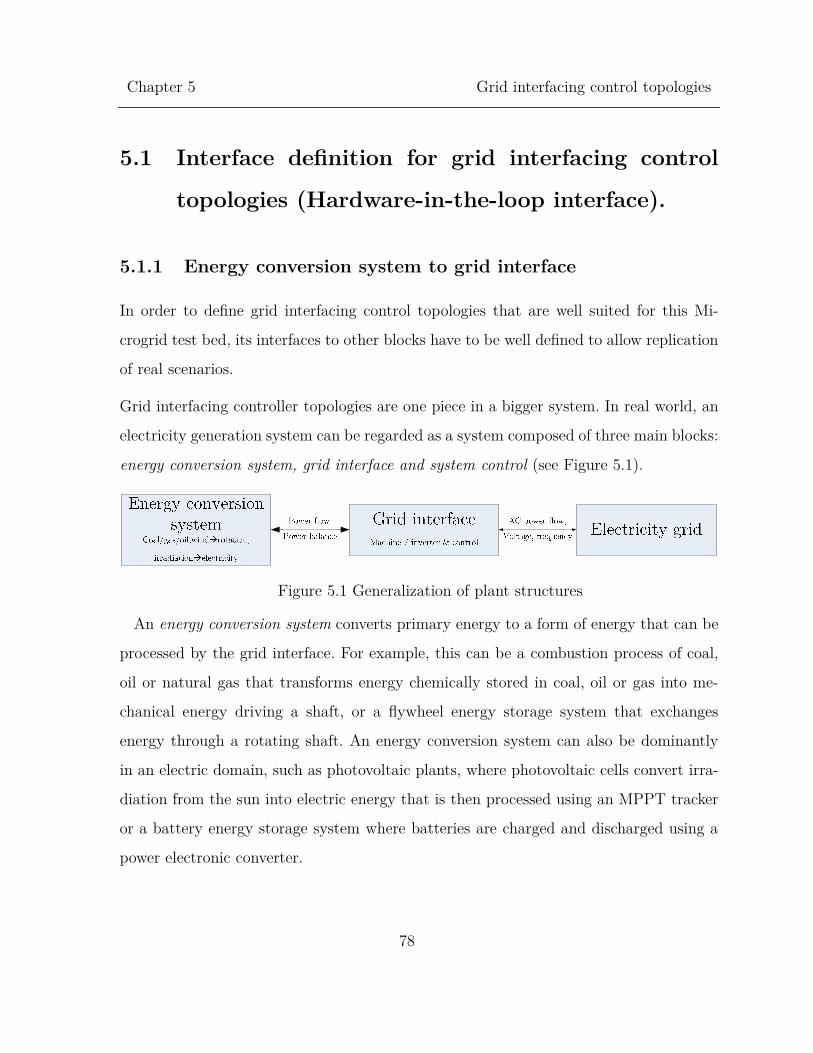
Chapter 5
Grid interfacing control topologies
78
5.1 Interface definition for grid interfacing control
topologies (Hardware-in-the-loop interface).
5.1.1 Energy conversion system to grid interface
In order to define grid interfacing control topologies that are well suited for this Mi-
crogrid test bed, its interfaces to other blocks have to be well defined to allow replication
of real scenarios.
Grid interfacing controller topologies are one piece in a bigger system. In real world, an
electricity generation system can be regarded as a system composed of three main blocks:
energy conversion system, grid interface and system control (see Figure 5.1).
Figure 5.1 Generalization of plant structures
An energy conversion system converts primary energy to a form of energy that can be
processed by the grid interface. For example, this can be a combustion process of coal,
oil or natural gas that transforms energy chemically stored in coal, oil or gas into me-
chanical energy driving a shaft, or a flywheel energy storage system that exchanges
energy through a rotating shaft. An energy conversion system can also be dominantly
in an electric domain, such as photovoltaic plants, where photovoltaic cells convert irra-
diation from the sun into electric energy that is then processed using an MPPT tracker
or a battery energy storage system where batteries are charged and discharged using a
power electronic converter.

Chapter 5
Grid interfacing control topologies
79
A grid interface picks up the energy made available from the energy conversion system
and transforms it into a form of electricity that the grid can accept and/or requires. For
hydro-thermal generation this can mostly be seen as the electric machine that generates
electricity out of rotational energy provided by the energy conversion system. The inter-
face between these two systems is mostly defined by the well-known swing equation,
relating the power flows between energy conversion system and grid interface (generator).
For mechanical storage systems, an electric machine realizes bidirectional power flow
following the same principle. Similarly for a photovoltaic plant, the grid interface is
formed by the VSI that converts energy coming from the MPPT converter into a form
of electricity that is acceptable or required by the grid. For a photovoltaic plant, often
the voltage on the inverter DC-bus, buffered by a capacitor, is an expression for power
flow balance. If the DC-bus voltage is above the nominal value, more power is to be
injected in the grid; less if the voltage is below nominal value [42]. The same structure
can apply to power electronic interfaced storage systems, such as battery energy storage
systems.
The decision on whether the grid interface or the energy conversion system governs
the short term energy production reference point depends on the role of the plant in the
electricity system. Typically, grid-following plants operate using an MPPT scheme which
clearly puts the active power command to the energy conversion system (example: pho-
tovoltaic systems, wind turbines). For systems operated in a droop fashion (hydro-ther-
mal plants, Diesel generators, hydro stations, grid-supporting converters in Microgrids…)
the grid interface or the coupling between energy conversion system and grid interface
determines the (re)active power command. For example, active power/frequency droop
is a consequence of the mechanical system in hydro-thermal plants described by the
swing equation. For grid-supporting converters in Microgrids, the control loop mimics

Chapter 5
Grid interfacing control topologies
80
these droops and therefore decides on the active and reactive power injection, whereas
the energy conversion system has to follow this command.
Certain restrictions in the short term and long term maximum and minimum active,
reactive and complex power injected by the grid interface exist, based on limitations of
plant sizing, long term or short term availability of primary energy, ramping constraints
and other limitations. For example, an energy conversion system has a maximum power
output, which is determined by its size, but also by the availability of primary energy
flow (coal, oil, gas, irradiation, wind, water flow…). Sometimes the grid interface’s rating
is lower than the power rating of the energy conversion system (often the case for pho-
tovoltaic plants). Lastly, the ramping of hydro-thermal generators can cause short term
limitations of available energy.
From these thoughts, a definition for the coupling of an energy conversion system
model and a grid interfacing control topology can be derived. The two main aspects
in this coupling for the most common generation systems are: active power
balance8 and limitations of electrical energy flow.
Hence, these two aspects are treated as the Hardware-in-the-loop interface
from the HIL software model (plant models9) to the hardware-based device
under test (grid interface control topology, VSI and AC Microgrid).
The feedback from the device under test to the software model, such as
measured power injection, voltage levels, current flow and system frequency,
8 Often, reactive power is a by-product within the grid interface, not of important concern for the
energy conversion system and therefore not an important part of the interface definition. 9 This thesis uses the term “plant model” when referring to the HIL software model implementation
of an energy conversion system.

Chapter 5
Grid interfacing control topologies
81
is provided through sensor measurements. The entire HIL interface is shown in
Figure 5.2.
Figure 5.2 Definition of HIL interface between plant model and grid interface
Detailed parameter explanation:
ᵃ����. This parameter can be set through a plant model to inform a grid inter-
facing control topology to inject ᵃ���� amount of active power into the grid. A
grid-feeding grid interface will follow this active power command. A droop con-
trolled grid interface generates and implements this command by itself and
ignores this HIL interface parameter. To ensure power balance in the generation
system, power limits are required.
ᵆ����. Similarly to ᵃ����, ᵃ���� is provided. For almost all plant models, reac-
tive power is not part of the plant model. One exception is the model of a ZIP
load, which contains governing equations for a reactive power set-point.
P/Q/S limits. Limits have various necessities from within the plant model
and the grid interface. In some cases – as outlined before – the energy conver-
sion system cannot deliver a certain amount of active power as requested by a

Chapter 5
Grid interfacing control topologies
82
grid interface (e.g., droop controlled). In this case, the grid interface power
output has to be limited temporarily to restore power balance.
5.1.2 Software interface: control topology to inverter
All grid interface control topologies have to output a quantity that can be handled by
the VSI. In this case, duty cycles can be used to generate the PWM pulses to turn on
and turn off the IGBTs at the right time instants. Therefore, all grid interface control
topologies in the abc or dq0 reference frame output three-phase duty cycles in.
5.2 Grid following controller
5.2.1 Control objective
The control objective of a grid-following converter is to inject/withdraw a certain amount
of active and/or reactive power into/from the grid to which it is connected [29], [42].
The reference value for this control topology can be formulated in terms of either power
or current. Current references indirectly translate to injected/withdrawn power
(ᵃ����,ᵃ����) through the connection point voltage.
5.2.2 Common use
Grid-following control topologies can commonly be used to realize the grid interface of
MPPT controlled plants or to mimic a load to the grid. For both types, it is known how
much power has to be injected or absorbed from the grid.

Chapter 5
Grid interfacing control topologies
83
5.2.3 Realization
In order to implement a grid-following converter that is based on a current-source, a
control loop structure as given in Figure 5.3 can be used. Essentially, it makes use of a
dq0 controller block (section 2.4.2) to provide a high performance current controller.
This controller is cascaded to an outer power controller that only consists of two PI
controllers for active and reactive power control. To synchronize to an existing grid, the
grid-following converter retrieves the grid voltage angle using a three-phase PLL block
as presented in section 2.6. This controller implementation has been adapted from con-
cepts in [31], [42]. It allows accurate control of four-quadrant power exchange at the
point of the ᵅ����� current sensors. The power exchange will be equivalent to power flow
at the PCC (Figure 5.3: “AC Microgrid bus”) except for magnetization currents of con-
nection transformers (if existent) and reactive power consumption due to connection
inductances ᵃ��.
Figure 5.3 Control loop structure using dq0 PI controllers for grid-following con-
verters
The calculation of active, reactive and complex power is performed in the natural
reference frame [58]:

Chapter 5
Grid interfacing control topologies
84
ᵃ� = ᵅ���ᵅ��� + ᵅ���ᵅ��� + ᵅ���ᵅ��� (5.1)
ᵃ� = 1√3
((ᵅ��� − ᵅ���)ᵅ��� + (ᵅ��� − ᵅ���)ᵅ�� + (ᵅ��� − ᵅ���)ᵅ���) (5.2)
ᵃ� = �ᵃ�� + ᵃ�� (5.3)
Power limiting capabilities are provided at the output of the power controller through
limiting the commanded current levels. The maximum power limit realizations are given
in equations (5.4)-(5.6). Minimum limits are realized similarly.
ᵃ������ = ᵃ����
3√
2ᵃ������ (5.4)
ᵃ������ = ᵃ����
3√
2ᵃ������ (5.5)
ᵃ���� = ᵃ����
3√
2ᵃ������ (5.6)
Available parameters and their default values are shown in Table 5.1.

Chapter 5
Grid interfacing control topologies
85
Table 5.1 Parameters of grid-following converter control loop topology
Parameter Description Default
value
Unit
ᵆ������ Proportional gain of PI power controllers (d & q) 0.003 �� or �
���
ᵆ������ Integral gain of power PI controllers (d & q) 1.8 ��×� or
�����
ᵆ������ Proportional gain of current PI controllers (d & q) 9 ��
ᵆ������ Integral gain of current PI controllers (d & q) 20010 ���
ᵆ���� Feed-forward gain for current controllers (0…1) 1.0 -
ᵆ��� Filter inductance value ᵃ�� for decoupling in current controller
1.15mH ᵃ�
ᵆ�ᵆ������� Enable decoupling in current controller True Boolean
ᵆ���� Maximum injected complex power (3 levels availa-ble11)
5000 VA
ᵆ���� Minimum injected complex power (3 levels available) -5000 VA
ᵆ���� Maximum injected active power (3 levels available) 5000 W
ᵆ���� Minimum injected active power (3 levels available) -5000 W
ᵆ���� Maximum injected reactive power (3 levels available) 5000 VAr
ᵆ���� Minimum injected reactive power (3 levels available) -5000 VAr
10 200 for cases with a weak grid. For grids with higher voltage stability, using values up to 900 �
�� is possible. Similarly ᵆ������ can be increased from 9 to 13.5 �
�. 11 In this case ‘levels’ refers to the ability to accept three different power limits and to only apply the
strictest.

Chapter 5
Grid interfacing control topologies
86
5.2.4 Simulation results
a. Simulation setup
In a PSIM simulation, the grid-following converter has been connected to a stiff grid
with 120V, 60Hz. Power reference steps have been given to the module to demonstrate
its ability for fast and reliable four-quadrant operation as given in Table 5.2.
Table 5.2 Simulation load power references
Time [s] Active power reference [W] Reactive power reference [VAr]
0 0 0
0.2 +5000 0
0.3 -5000 0
0.4 0 0
0.5 0 +5000
0.6 0 -5000
0.7 0 0
b. Results
Figure 5.4 shows the resulting active and reactive power injections by the grid following
converter module. It can be seen that a fast, stable and smooth power control is possible
in all four quadrants. Within about 8-12ms the reference power value can be reached.
The current waveforms at the reference step at time t=0.2 are shown in Figure 5.5. The
THD of these currents is at about 1.8%.

Chapter 5
Grid interfacing control topologies
87
Figure 5.4 Active and reactive power injection upon power reference steps for P & Q
Figure 5.5 Output currents ᵅ������ upon a reference step from P=0W to P=5000W
(Q=0)

Chapter 5
Grid interfacing control topologies
88
5.3 Voltage-source based droop controller
5.3.1 Control objective
The control objective of a voltage-source based droop controller is to form or support a
Microgrid. In order to be able to form such a grid, an active and direct control of the
connection voltage and frequency is required. When working together with other droop
controlled converters, this control topology employs a drooping scheme in order to share
active and reactive power in a decentralized control organization. This control topology
is part of the primary level of Microgrid control.
5.3.2 Common use
A voltage-source based droop controller can commonly be used with dispatchable gen-
erators and appropriately sized storage systems. Limitation of output power without
adjustment of droop gains is difficult to achieve with this control topology. Therefore,
its use with MPPT controlled plants is less feasible.
5.3.3 Realization
The voltage-source based droop controller employs a three stage cascaded control struc-
ture [29], [31]. Figure 5.6 shows a base version for balanced load currents. An inner
current control loop ensures a good current waveform, fast transients and decoupling of
d and q channels. An outer voltage control loop allows to control the converter filter
capacitor voltage (ᵅ��) to a pre-determined level. The droop controller provides a defini-
tion of the reference voltage, reference frequency and system angle using the droop equa-
tions presented in section 2.7.1.

Chapter 5
Grid interfacing control topologies
89
Figure 5.6 Basic voltage-source based droop controller implementation
Transformer magnetization currents of common distribution transformers can be un-
balanced and contain harmonics. For this reason the voltage control loop has been ex-
tended by using a negative sequence controller as introduced in section 2.7.4. It can be
activated upon request to provide balanced output voltages under the presence of un-
balanced load currents.
To provide better droop controller transient performance and easier grid synchroni-
zation, the concepts of virtual impedance, power droop decoupling (sections 2.7.2 and
2.7.3) and derivative droop gains (section 2.7.1) have been made available in this topol-
ogy. The final controller implementation is shown in Figure 5.7. Configuration parame-
ters with default parameters are shown in Table 5.3.

Chapter 5
Grid interfacing control topologies
90
Figure 5.7 Complete voltage-source based droop controller implementation
Table 5.3 Parameters of voltage-source based droop controller topology
Parameter Description Default
value
Unit
ᵆ�������� Proportional gain of P’/f droop controller 0.00004 ���
ᵆ�������� Proportional gain of Q’/V droop controller 0.0002 ����
ᵆ��������� Derivative gain of P’/f droop controller 0.02 ��×��
ᵆ��������� Derivative gain of Q’/V droop controller 0.01 �����
ᵆ�� Nominal system frequency 60 ᵃ�ᵅ�
ᵆ�� Nominal system voltage (RMS) 120 ᵃ����

Chapter 5
Grid interfacing control topologies
91
ᵆ�� Nominal active power injection 0 W
ᵆ�� Nominal reactive power injection 0 VAr �� Assumed X/R ratio 500 -
ᵆ�� Virtual output inductance 0.003 H
ᵆ�� Virtual output resistance 0 Ω
ᵆ������� Proportional gain of voltage PI controllers (d & q) 0.4 ��
ᵆ������� Integral gain of voltage PI controllers (d & q) 25.0 ���
ᵆ����� Feed-forward gain for voltage controllers (0…1) 0.0 -
ᵆ��� Filter capacitance value ᵃ�� for decoupling in voltage controller
50μF F
ᵆ�ᵆ�������� Enable decoupling in voltage controller True Boolean
ᵆ�ᵆ�������� Enable negative sequence voltage controller False
ᵆ������ Proportional gain of current PI controllers (d & q) 13.5 ��
ᵆ������ Integral gain of current PI controllers (d & q) 675 ���
ᵆ���� Feed-forward gain for current controllers (0…1) 1.0 -
ᵆ��� Filter inductance value ᵃ�� for decoupling in current controller
1.15mH ᵃ�
ᵆ�ᵆ������� Enable decoupling in current controller True Boolean
ᵆ���� Maximum injected complex power (3 levels availa-ble12)
5000 VA
ᵆ���� Minimum injected complex power (3 levels available) -5000 VA
ᵆ���� Maximum injected active power (3 levels available) 5000 W
ᵆ���� Minimum injected active power (3 levels available) -5000 W
ᵆ���� Maximum injected reactive power (3 levels available) 5000 VAr
ᵆ���� Minimum injected reactive power (3 levels available) -5000 VAr
12 In this case ‘levels’ refers to the ability to accept three different power limits and to only apply the
strictest.

Chapter 5
Grid interfacing control topologies
92
5.3.4 Simulation results
a. Simulation setup - Stand-alone operation
One simulation module with a voltage-source based droop controller has been simulated
with a PQ load, in order to evaluate the stability. The simulation setup is given in Figure
5.8.
Figure 5.8 Voltage-source based droop controller: stand-alone simulation block
structure
The PQ load changes its demand according to Table 5.4.
Table 5.4 PQ load schedule
Time [s] Complex power reference [VA] Power factor reference
1 0 1
1.35 2500 1
1.7 5000 1
1.8 5000 0.9
1.9 2500 0.9
2.2 0 0.9

Chapter 5
Grid interfacing control topologies
93
The implementation of this voltage-source based droop controller in simulation is
equivalent to the descriptions in section 5.3.3 except that no negative sequence control
loop is present, since an accurate and fast model of the non-linear, unbalanced trans-
former magnetization currents is difficult to achieve in circuit simulators. The function-
ality of the negative sequence control loop is demonstrated in the experimental imple-
mentation in section 10.2.1c.
b. Stand-alone operation
At first, in Figure 5.9, it is demonstrated that the voltage-source based droop controller
is capable of forming a stand-alone grid with a clean grid voltage and good voltage
stability during transients. Figure 5.10 displays power balances between generation and
load, as well as transient behavior upon load requests for the entire rated power range
at power factor 1 and 0.9. It can be seen that the power demand is supplied. The con-
stant reactive power offset between inverter injection and PQ load results from the
transformer magnetization that the inverter constantly has to provide. This value is
about 800VAr at nominal grid frequency and has been determined experimentally based
on the chosen transformer.

Chapter 5
Grid interfacing control topologies
94
Figure 5.9 Inverter capacitor voltages (a) and output currents (b) when PQ load
step change from 0W to 2500W is performed
Figure 5.10 Inverter output power and PQ power load references (a) and inverter
output currents (b) for entire load schedule

Chapter 5
Grid interfacing control topologies
95
c. Simulation setup – Power sharing
In extension to the previous simulation, a second simulation module is connected in
parallel with the first module, resulting in the simulation structure shown in Figure 5.11.
The PQ load now operates with twice the complex power references given in Table 5.4
and the same power factor values.
Figure 5.11 Voltage-source based droop controller: power sharing simulation block
structure
In this scenario, varying system frequency and connection voltages should indicate the
decentralized power sharing that is typical to droop controllers.
d. Power sharing
Figure 5.12 shows power injections and transformer currents (Δ side) for both simulation
modules, as well as the system frequency and load RMS voltage level. The simulation
demonstrates a stable and fast load sharing between the two modules.

Chapter 5
Grid interfacing control topologies
96
Figure 5.12 Power sharing between two voltage-source droop controllers under vary-
ing load conditions
Chapter 5
Grid interfacing control topologies
97
5.4 Current-source based droop controller
5.4.1 Control objective
The control objective of a current-source based droop controller is to support an existing
grid-connected or islanded Microgrid. This converter role is not able to form a grid by
itself. When working together with other droop controlled converters, this control topol-
ogy employs a drooping scheme in order to share active and reactive power in a decen-
tralized control organization. This control topology is part of the primary level of Mi-
crogrid control.
5.4.2 Common use
A current-source based droop controller can commonly be used with dispatchable gen-
erators and well sized storage systems. Limitation of output power without adjustment
of droop gains is easily realizable with this control topology. Therefore, its use with
MPPT controlled plants is feasible, neglecting possible restrictions from the energy con-
version system or higher level grid control issues. With slight adjustments, this topology
can also be used for power curtailment scenarios under exceptional grid conditions (for
example, during excessive system frequencies [59]).
5.4.3 Realization
The current-source based droop controller employs a three stage cascaded control
structure [29] as shown in Figure 5.13. It is an extension to the grid-following converter
control implementation. An inner current control loop ensures a good current waveform,
fast transients and decoupling of d and q channels. An outer power control loop ensures

Chapter 5
Grid interfacing control topologies
98
the injection of active and reactive power as determined by the third controller stage.
This third stage implemented the droop equations, solved for ᵃ� and ᵃ� as reference
values. System voltage and system frequency are inputs to this droop controller. System
angle and frequency are determined by a three-phase PLL. Filter on voltage and fre-
quency provide smooth signals, when the detection mechanisms are noisy.
Configuration parameters of this control topology with default parameters are given in

Chapter 5
Grid interfacing control topologies
99
Table 5.5.
Figure 5.13 Current-source based droop controller implementation

Chapter 5
Grid interfacing control topologies
100
Table 5.5 Parameters of current-source based droop controller topology
Parame-
ter
Description Default
value
Unit
ᵆ�������� Proportional gain of P/f droop controller 10000 ���
ᵆ�������� Proportional gain of Q/V droop controller 50 ����
ᵆ�� Nominal system frequency 60 ᵃ�ᵅ�
ᵆ�� Nominal system voltage (RMS) 120 ᵃ����
ᵆ�� Nominal active power injection 0 W
ᵆ�� Nominal reactive power injection 0 VAr
ᵆ�� Virtual output inductance 0 H
ᵆ�� Virtual output resistance 0 Ω
ᵆ������ Proportional gain of power PI controllers (P & Q) 0.003 �� or �
���
ᵆ������ Integral gain of power PI controllers (P & Q) 1.8 ��� or
�����
ᵆ������ Proportional gain of current PI controllers (d & q) 9 ��
ᵆ������ Integral gain of current PI controllers (d & q) 200 ���
ᵆ���� Feed-forward gain for current controllers (0…1) 1.0 -
ᵆ��� Filter inductance ᵃ�� for decoupling in current controller 1.15mH ᵃ�
ᵆ�ᵆ������� Enable decoupling in current controller True Boolean
ᵆ���� Maximum injected complex power (3 levels available13) 5000 VA
ᵆ���� Minimum injected complex power (3 levels available) -5000 VA
ᵆ���� Maximum injected active power (3 levels available) 5000 W
ᵆ���� Minimum injected active power (3 levels available) -5000 W
ᵆ���� Maximum injected reactive power (3 levels available) 5000 VAr
ᵆ���� Minimum injected reactive power (3 levels available) -5000 VAr
13 In this case ‘levels’ refers to the ability to accept three different power limits and to only apply the
strictest.

Chapter 5
Grid interfacing control topologies
101
5.4.4 Simulation results
a. Simulation setup
Because the current-source based droop controller cannot form a grid by itself, it has
been simulated in cooperation with a voltage-source based droop controller as shown in
Figure 5.14.
Figure 5.14 Simulation configuration
The load profile applied is included in the simulation results (Figure 5.15).
b. Results
In the results it becomes apparent, that the two droop controllers share the load power.
However, the reaction speeds of the two droop control methods are different, because
the current-source based droop controller has to strongly filter the connection voltage
and frequency for its droop controller. Improved frequency and voltage detection meth-
ods are advantageous for this kind of droop controller resulting in a faster response
during transients.

Chapter 5
Grid interfacing control topologies
102
Figure 5.15 System parameters in a simulation with one voltage-source based droop
controller (module 2) and one current-source based droop controller (module 1) in par-
allel

Chapter 6
Load and generation plant modelling
103
Chapter 6
Load and generation plant model-
ling
6.1 Introduction
This chapter describes modeling of loads and energy conversion systems (plant model-
ing). Software-based real-time simulation of loads and generation plants generates input
parameters to the hardware implemented part of the HIL Microgrid test bed. As men-
tioned in the previous chapter, plant models connect with grid interfacing control topol-
ogies using a standardized set of parameters and variables:
Active & reactive power command
Active, reactive & complex power limit
Sensor measurements
The following sections describe the model design of a “ZIP load”, a photovoltaic plant
and a generic storage system.

Chapter 6
Load and generation plant modelling
104
6.2 Load model
The goal of this model is to define a generic model for a three-phase balanced and linear
load connected to distribution systems. The most common way to model these loads is
including three types of loads: constant impedance, constant current and constant power
w.r.t. to voltage variations. This model is called “ZIP load”.
The ZIP load equations are [60]:
ᵃ���� = ᵃ�� �ᵃ�� �ᵃ�ᵃ��
��+ ᵃ��
ᵃ�ᵃ��
+ ᵃ�� � (6.1)
ᵃ���� = ᵃ�� �ᵃ�� �ᵃ�ᵃ��
��+ ᵃ��
ᵃ�ᵃ��
+ ᵃ��� (6.2)
where ᵃ�� and ᵃ�� are the active and reactive load power at nominal voltage level ᵃ��, ᵃ�
is the actual connection voltage and ᵃ�� , ᵃ�� , ᵃ�� ,ᵃ��, ᵃ��, ᵃ�� are the ZIP load parameters
for constant impedance (ᵃ�� ,ᵃ��), constant current (ᵃ�� , ᵃ��) and constant power (ᵃ�� , ᵃ��)
for active and reactive power. The ZIP load parameters allow the definition of load power
behavior under changing voltage levels. Common ZIP parameters for different scenarios
are reported in [60], [61]. The ZIP load does not characterize any non-linear loads.
This ZIP load model can be used to obtain reference command powers for the grid-
following control topology. Power limitations can be introduced to reflect the sizing of a
particular load. ᵃ�� and ᵃ�� can be used to realize a time dependent load profile.

Chapter 6
Load and generation plant modelling
105
6.3 Photovoltaic plant model
6.3.1 Objective and simplifications
The objective for a photovoltaic plant model is to replicate a common PV plant for the
Microgrid test bed HIL software simulation using a real-time model representation. It is
based on the central inverter PV plant configuration [62] that is common for residential
PV plants. A central inverter is based on one array of n × m PV modules, blocking
diodes, a single DC/DC MPPT converter and a single inverter. (Multi-)String inverters
are used to improve the central inverter performance under partial shading or other
unbalanced operating conditions. Since the solution of a PV cell model is computation-
ally expensive, this PV plant model has been based on a single PV cell model represent-
ing the entire array. This results in balanced operating conditions among the entire array
(solar insolation, temperature, dirt and parameter variances). For such a configuration,
there is no difference between a central and (multi-)string inverter configuration.
Compatibility with the grid-following control topology is required due to MPPT op-
eration, but compatibility with the current-source based droop control topology is also
possible.
6.3.2 Model structure
The PV plant model in Figure 6.1 consists of components that are also commonly
used in real PV plants.

Chapter 6
Load and generation plant modelling
106
Figure 6.1 Structure of the PV plant implemented
Common components are:
PV array. A PV array consists of n× m PV modules. As mentioned before,
this plant model uses one scaled PV cell model to represent the array. Ideal
blocking diodes are taken into account.
MPPT converter. In order to allow maximum power extraction, a DC/DC
converter sets the maximum power condition for the PV array. Depending on
the system configuration, buck, boost or buck-boost converters are common.
To provide a high flexibility, a buck-boost converter is assumed here. However,
given an appropriate mathematical model, buck or boost converters could also
be used. The buck-boost converter is represented using an averaged converter
model for discontinuous and continuous conduction modes of operation includ-
ing non-ideal parameters, such as inductor ESR.

Chapter 6
Load and generation plant modelling
107
MPPT tracking algorithm. A common hill-climbing method is the incre-
mental conductance algorithm, offering convergence to a local maximum power
point (MPP). It offers zero oscillations at steady-state if configured correctly.
Grid inverter. Typically, a single- or three-phase inverter converts the output
power of the MPPT converter into AC power. The control objective of this
inverter is to regulate the DC-bus voltage ᵃ��� to a certain value by increasing
or decreasing the AC power output. To accomplish this, in this test bed, a switch
from the HIL software model to the HIL device under test has to be performed.
For this reason, the grid inverter is represented by an ‘HIL grid interface’ on
the software model side. The HIL grid interface links the software model with
real hardware by imitating the grid inverter behavior in both domains.
Curtailment. Depending on the plant size, grid codes, grid interfacing con-
troller requirements or current operating conditions, curtailment of PV output
power or power injection into the grid can become necessary. Therefore algo-
rithms to limit PV power production or grid power injection to restore ᵃ��� close
to nominal values is implemented.
It has to be noted that the DC-bus voltage V�� of this photovoltaic model is a numeric
model parameter and has no relation to the DC-bus realized in the test bed (Figure 3.1
on page 46)! In the test bed hardware, only the Microgrid AC bus is part of a genera-
tor/load simulation.

Chapter 6
Load and generation plant modelling
108
6.3.3 Mathematical formulation
a. PV array
The PV array is represented by a single-diode PV cell model and a reverse blocking
diode. Nomenclature for the following model is given in Table 6.1.
Table 6.1 Nomenclature for PV cell model
Parameter PV module definitions
ᵃ�� Number of cells in series
ᵃ��� Number of modules in series
ᵃ��� Number of modules in parallel
ᵃ�� standard light intensity in ���
ᵃ���� Module reference temperature in Kelvin
ᵃ�� Series resistance in Ohm
ᵃ�� Parallel resistance in Ohm
ᵃ���� Nominal short circuit current
ᵃ��� Nominal diode saturation current at ᵃ����
ᵃ�� Band energy in eV
ᵃ� Ideality factor
ᵅ�� Short circuit/temperature coefficient in ��
ᵃ��� Open circuit voltage in V
ᵃ��� Voltage at MPP in V
ᵃ��� Current at MPP in A
ᵃ�� Temperature of module surroundings in Kelvin
ᵃ�ᵃ�ᵃ�ᵃ� Nominal operating temperature in degree Celsius
ᵃ� Light intensity on module in ���
ᵅ� electron charge in C

Chapter 6
Load and generation plant modelling
109
ᵅ� Boltzmann constant in ��
ᵃ� Module temperature in K
ᵃ��� Photovoltaic current (current of current source in 2 diode model) in A
ᵃ�� Temperature specific reverse diode saturation current in A
ᵃ����� Terminal voltage of PV module in V
ᵃ����� Terminal current of PV module in A
ᵅ�ᵅ�ᵅ�ᵃ�ᵅ�ᵃ�ᵅ�ᵃ�ᵃ� Maximum error that is allowed to regard a solution as converged
Parameter Bypass diode Db definitions
��� Ideality factor of Db
���� Reverse saturation current of Db
The cell output current can be expressed as a function of the terminal voltage [63]:
ᵃ����� = ᵃ���� − ᵃ�� �ᵃ�������+���������� � − 1� − ᵃ����� + ᵃ��ᵃ�����
ᵃ��
− ᵃ����⎝⎜⎛ᵃ�
− ����������� − 1
⎠⎟⎞
(6.3)
With
ᵃ�� = ᵅ�ᵃ�ᵅ�
ᵃ��� (6.4)
ᵃ���� = �ᵃ����� + ᵃ��ᵮ�� � ᵃ�ᵃ��
(6.5)
ᵃ�� = ᵃ���� �ᵃ��ᵃ�
��ᵃ��
����� � �
��−�
��� (6.6)

Chapter 6
Load and generation plant modelling
110
ᵃ���� =ᵃ�����
ᵃ����������� − 1
(6.7)
For an ideal PV module under equal irradiation and temperature conditions:
ᵃ����������� = ᵃ���ᵃ����� (6.8)
ᵃ����������� = ᵃ���ᵃ����� (6.9)
Since equation (6.3) is a transcendental equation, no direct analytical solution exists.
Based on [64], computationally fast methods to evaluate this equation are of Newton-
Raphson and the Lambert-W function.
Newton-Raphson solutions can be obtained faster, if using Halley’s update method,
precomputed fixed values (PFV) or model parallelization. This thesis employs an imple-
mentation based on the Newton-Raphson scheme with precomputed fixed values.
PFV aims at simplifying all computations by replacing multiple mathematical opera-
tions on constant values with one constant value that is only computed once per model
life time, once per model execution or once per Newton-Raphson iteration.
The solution of a PV cell model using Newton-Raphson without PFV implemented in
C++ on a 3GHz Intel Core i5 processor took 1.37ᵰ�ᵅ� to compute, on average (45000
samples taken). Using Newton-Raphson with PFV accelerated the solution to 1.025ᵰ�ᵅ�,
on average (-25%). This execution time is likely sufficient for a PV plant execution
window of 100ᵰ�ᵅ� per model computation on the chosen microcontroller. As mentioned
before, further optimizations can increase computational speed so that multiple cell
models for partial shading simulations could be implemented, if desired (e.g., using [65]).
Model verification. To verify the proper function of this PV module model, the
computational results obtained from a C++ implementation using Newton-Raphson
with PFV have been compared to the PSIM model of a PV module. Module parameters

Chapter 6
Load and generation plant modelling
111
for the Bosch c-SI M2453BB module have been taken from [63], [66], [67]. Figure 6.2
shows that the results match very well.
Figure 6.2 PV model simulation in PSIM vs. computation in implemented C++
model for Bosch c-SI M2453BB PV module
b. MPPT converter model
The average model of a buck-boost converter has to be valid for discontinuous and
continuous conduction modes of operation. The inclusion of non-ideal parameters in
circuit components allows to model a lossy converter and to obtain system dynamics
accordingly. Nomenclature and a derivation for the model equations presented here are
available in appendix A.5 on page 210 ff.
The state equations of the average model based on Figure A.6 are:

Chapter 6
Load and generation plant modelling
112
ᵃ� ᵃ�ᵅ��ᵃ�ᵅ�
= ᵅ��[−ᵃ�� − ᵃ��(ᵃ��� + ᵃ����) − ᵃ��(ᵃ��� + ᵃ����)] + ᵃ��ᵃ��� − ᵃ��ᵃ���
+ ᵃ��ᵅ���ᵃ��� + ᵃ��ᵅ����ᵃ��� − ᵃ��ᵃ���� − ᵃ��ᵃ���� (6.10)
ᵃ��ᵃ�ᵅ���ᵃ�ᵅ�
= ᵅ��� − ᵃ��ᵅ�� (6.11)
ᵃ��ᵃ�ᵅ���ᵃ�ᵅ�
= ᵃ��ᵅ�� − ᵅ���� (6.12)
The converter input and output voltages can be given as:
ᵅ��� = ᵅ��� + (ᵅ��� − ᵃ��ᵅ��)ᵃ��� (6.13)
ᵅ���� = ᵅ��� + (ᵃ��ᵅ�� − ᵅ����)ᵃ��� (6.14)
Figure 6.3 Definition of ᵃ��, ᵃ�� and ᵃ�� at the example of discontinuous inductor cur-
rent
The duty cycles ᵃ�� and ᵃ�� indirectly describe the mode of operation (see illustration
in Figure 6.3) and are defined as follows, assuming ᵃ�� = ᵃ� = model input parameter:
ᵃ������ = 1 − ᵃ�� (6.15)
ᵃ�� =⎩�⎨�⎧ᵃ���ᵅ��� − ᵅ�� − ᵪ��̅(ᵃ��� + ᵃ�� + ᵃ��)�
ᵅ����− Δᵃ��|��
ᵃ�ᵃ��ᵅ����
ᵃ�� ≤ ᵃ������
ᵃ������ ᵅ�ᵅ�ℎᵃ�ᵅ�ᵅ�ᵅ�ᵅ�ᵃ� (6.16)

Chapter 6
Load and generation plant modelling
113
ᵃ�� = �1 − ᵃ�� − ᵃ�� ᵃ�� < 1 − ᵃ��0 ᵅ�ᵅ�ℎᵃ�ᵅ�ᵅ�ᵅ�ᵅ�ᵃ�
(6.17)
Also, due to continuous PWM activity, there is a minimum average inductor current.
A lower inductor current may not be allowed by the model
ᵃ������ = ᵃ���ᵅ��� − ᵅ�� − ᵪ��̅(ᵃ��� + ᵃ�� + ᵃ��)�
2ᵃ��ᵃ�(ᵃ�� + ᵃ��) (6.18)
ᵅ�� = �ᵅ�� ᵅ�� ≥ ᵅ������
ᵅ������ ᵅ�ᵅ�ℎᵃ�ᵅ�ᵅ�ᵅ�ᵅ�ᵃ� (6.19)
For verification purposes, the average model has been compared with a standard cir-
cuit simulator. In the test scenario, the input voltage is constant at 100V. The load
current ᵃ���� is 1.1A during the first 2500 data points (2.5 seconds) and 8A afterwards.
At time 5s (data point 5000) a duty cycle step change from 0.5 to 0.55 is performed,
resulting in a higher output voltage. In Figure 6.4 it can be seen that the average model
matches the circuit simulation quite well; however, slight differences during the first 2500
data points (DCM) are apparent. In future work, the model accuracy during DCM has
to be improved to better represent this state of operation that is mostly common during
start-up, some transient and low PV output situations.

Chapter 6
Load and generation plant modelling
114
Figure 6.4 Comparison of average model with circuit simulation. Blue: ᵃ���� average
model; red: ᵃ���; Green: ᵃ���� PSIM simulation
c. MPPT algorithm
The chosen MPPT algorithm is “incremental conductance” which is a hill climbing al-
gorithm. Generally, this algorithm uses three equations to determine the current location
on the P-V plot for a photovoltaic array [68]:
ᵃ�ᵃ�ᵃ�ᵃ�
= − ᵃ�ᵃ�
ᵃ�ᵅ� ᵃ�ᵃ�ᵃ� (6.20)
ᵃ�ᵃ�ᵃ�ᵃ�
> − ᵃ�ᵃ�
ᵅ�ᵃ�ᵃ�ᵅ� ᵅ�ᵃ� ᵃ�ᵃ�ᵃ� (6.21)
ᵃ�ᵃ�ᵃ�ᵃ�
< − ᵃ�ᵃ�
ᵅ�ᵅ�ᵃ�ℎᵅ� ᵅ�ᵃ� ᵃ�ᵃ�ᵃ� (6.22)
Based on these decisions, the MPPT reference voltage is incremented or decremented
using a fixed step size.

Chapter 6
Load and generation plant modelling
115
d. HIL grid interface / grid inverter model
The HIL grid interface, shown in Figure 6.5, generates a reference AC power injection
based on the DC-bus voltage of the PV plant model. It uses a PI controller and deter-
mines the DC output current in the PV plant model based on the measured AC power
injection into the AC Microgrid.
Figure 6.5 HIL grid interface block structure
e. PV power curtailment
If the PV array output power is higher than the power absorbed from the model DC-
bus by the HIL grid interface (for inverter sizing reasons, for example), ᵃ��� will rise
above its nominal value. In this case, the PV array power output has to be limited.
PV curtailment is activated when an upper ᵃ��� threshold ᵃ������������ is surpassed. A
PI controller will then be used to regulate the error ᵃ������������ − ᵃ��� > 0 to zero. In
order to do so, the MPPT algorithm can be overridden and operated based on an input
reference voltage offset ᵃ����������� (compare to Figure 6.1 on page 106). With PV curtail-
ment active, the MPPT algorithm will keep its internal reference voltage constant and
will output the sum of this internal reference voltage and ᵃ�����������. This allows to in-
crease ᵃ��� beyond the MPP so that the PV output power is reduced.

Chapter 6
Load and generation plant modelling
116
f. Grid interface curtailment
In situations where a grid interface control topology decides on the injected active power
(droop control, for example) it is possible that there is less PV output power available
than injected by the grid interface. In this case the model DC-bus voltage will fall below
the nominal value. To avoid ᵃ��� collapse, a lower threshold ᵃ������������ has been defined,
below which a PI controller will temporarily introduce an active power output limit on
the grid interface to restore ᵃ��� to at least ᵃ������������. Thus, every grid interface control
topology must implement active power limits that can be changed at runtime by a plant
model.
6.3.4 Implementation
The implementation on the F28377D microcontroller mostly uses a dedicated CPU core
(CPU2) to compute the model at control loop speed (10.2 kHz). The entire PV plant
model can be computed within about 19ᵰ�ᵅ� out of about 100ᵰ�ᵅ� available. This clearly
indicates that there is enough room for future expansions, such as to incorporate multiple
PV cell computations per PV plant computation. More details on general implementa-
tion and experimental results are given in subsequent chapters.
6.4 Storage plant model
6.4.1 Objective
The objective of this plant is to provide a very simple representation of a generic energy
storage system (ESS). Most available storage technologies, such as batteries (Li-Ion,

Chapter 6
Load and generation plant modelling
117
Lead Acid…), compressed air energy storage, flywheel and pumped hydro, have charac-
teristics that can be generalized in their technical description to a certain extent. Some
very common characteristics describing the storage functionality of energy storage sys-
tems are:
Maximum and minimum power output in all system states
Maximum power ramping rate at all system states
Maximum and minimum energy that can be stored
Minimum uptimes, minimum downtimes
Storage system efficiency (during charging, storage and discharging)
Change of amount of energy stored and storable over time
Influences on internal parameters from the environment, such as temperature
This thesis limits the modeling of a storage plant to a formulation that takes into
account the maximum and minimum power output in various system states and the
amount of energy that can be stored, only. All other parameters are neglected at this
stage.
6.4.2 Mathematical formulation
The nomenclature for the formulation of the storage plant model is given in Table 6.2.
Positive active power ᵃ��� refers to an active power flow from the simulation module to
the Microgrid.

Chapter 6
Load and generation plant modelling
118
Table 6.2 Nomenclature for storage plant model
Parameter PV module definitions
ᵃ�� Energy stored in the ESS
ᵃ���� Maximum amount of energy that can be stored in this ESS
ᵃ��� Active power injected into the Microgrid on the AC side
ᵃ��� Power flowing from storage system to VSI
ᵰ���� Assumed efficiency of VSI
ᵃ�ᵃ�ᵃ� State-of-charge
ᵃ������� Maximum active power that can be absorbed by the ESS
ᵃ�������� Maximum active power that can be delivered by the ESS
ᵃ�ᵃ���� = ᵃ�ᵃ����ᵃ�ᵃ�ᵃ�ᵃ��
��� ���> 0 Slope of maximum power limit (absorption and delivery) in �
���� starting at 0W/0%SOC. This is valid until ����,�� or ����,��� ap-
ply, respectively
ᵃ�ᵃ����� = ᵃ�ᵃ����ᵃ�ᵃ�ᵃ�ᵃ��
��� ����< 0 Slope of maximum power limit (absorption and delivery) in �
���� ending at 0W/100%SOC. This is valid until ����,�� or ����,���
apply, respectively.
ᵅ���� Simulation speed ratio: simulation time speed / real world time speed. Can be used to perform experiments that are run at other
speeds than real-time speed.
The amount of energy stored in the ESS related to its current maximum capacity can
be expressed as state-of-charge:
ᵃ�ᵃ�ᵃ� = ᵃ��ᵃ����
(6.23)
While energy is flowing from storage system to AC grid the stored energy �� is
changing according to:
ᵃ�� = �− ᵃ���ᵰ����
ᵅ����ᵃ�ᵅ� (6.24)

Chapter 6
Load and generation plant modelling
119
While energy is flowing from the AC grid to the storage system the stored energy ��
is changing according to:
ᵃ�� = �−ᵃ���ᵰ����ᵅ����ᵃ�ᵅ� (6.25)
Power limiting is defined in relation to SOC as shown in Figure 6.6 and Table 6.2
(using ᵃ�������, ᵃ��������, ᵃ�ᵃ����, ᵃ�ᵃ�����). In order to allow a slow recovery from 0%SOC
or 100%SOC, the maximum charging power at 0%SOC and the maximum discharging
power at 100% are held at 10% × ᵃ������� or 10% × ᵃ�������� respectively. This ensures
that when the SOC has reached 0% or 100%, the storage is able to go back to an SOC
range between 0% and 100%.
Figure 6.6 Basic operation principle of generic storage plant
This storage plant is typically used together with a voltage-source based droop con-
troller to provide stable grid support or to form a grid. It is the responsibility of the
system designer and the grid interface to handle ESS power or energy limitations appro-
priately.
Storage system technology-specific models of a technology-specific storage plant have
been left for future work.
%SOC
PoutPmaxout
Pmaxin
dPlow dPhigh
0
Permissib
le power r
ange
100%

Chapter 7
Test bed simulation using a circuit simulator
120
Chapter 7
Test bed simulation using a circuit
simulator
So far, single components of this test bed have been tested in stand-alone operation or
together with some test bed components. The final goal of this thesis is to provide a
simulation of a 24-profile with four grid participants which requires simultaneous use of
all developed components. One simulation module represents a load to the grid, two
other simulation modules ensure a stable grid (storage plants) and the fourth simulation
module represents an intermittent DG: a photovoltaic plant. 24-hour profiles for load
and PV have been derived. The entire setup has been simulated using the simulation
software PSIM, version 9.1.3.

Chapter 7
Test bed simulation using a circuit simulator
121
7.1 Simulation setup
The following modules are included in the simulation:
Table 7.1 Test bed simulation configuration
Module Grid interface control topology Plant simulation
Load Grid-following converter ZIP Load
Photovoltaic Grid-following converter Photovoltaic plant
Storage (large) Voltage-source based droop controller Storage plant
Storage (small) Voltage-source based droop controller Storage plant
DC-bus voltage controller module
n/a n/a
All modules work with a maximum power of 5kVA. The simulation configuration is
shown in Figure 7.1.

Chapter 7
Test bed simulation using a circuit simulator
122
Figure 7.1 PSIM test bed system simulation – main page

Chapter 7
Test bed simulation using a circuit simulator
123
7.2 Load and solar insolation profiles
A common load profile for remote communities in Canada [69] has been adapted to
obtain a load profile for this simulation. The peak load is 1500VA with an assumed
power factor of 0.9. The total energy consumed during one day is 21.4 kWh.
The solar irradiation profile has been derived from data of the University of Waterloo’s
weather station14. A summer day with shading pattern was July 15th, 2014. The PV plant
is sized such that its peak PV power output for the given profile is close to 5kW. The
VSI efficiency is assumed to be constant: 95% (the actual VSI efficiency is a function of
output power and will have to be determined in the future).
Both profiles are depicted in Figure 7.2.
Figure 7.2 Solar insolation and load profile for 24 hours
7.3 Results
The results of the simulation described above are shown in Figure 7.3. The PV plant
follows the insolation profile in its active power injection during this day. It does not
14 http://weather.uwaterloo.ca

Chapter 7
Test bed simulation using a circuit simulator
124
inject or absorb any reactive power. The load absorbs power from the grid according to
its load profile with a constant power factor of 0.9. Both storage systems share the
burden of matching demand with generation. Due to the droop gain configuration, the
smaller storage system participates with only half of the energy the large storage system
handles. Together, the two storage systems form a droop controlled, islanded grid. Due
to the absence of secondary control, the system state can easily be read from system
frequency and RMS voltage. The storage models of the large and small units have been
sized for 20 kWh and 10 kWh, respectively. Since the storage modules share the load
proportionally to their sizing their SOC values are very close for the entire time (Figure
7.5). The initial SOC was set to 45%.
The DC-bus voltage controller module compensates for all inverter losses in the test
bed. For the simple switching loss modeling applied, according to the simulation, this
means that a maximum power of about 240W needs to be replaced by this module in
order to keep the test bed operational.
The photovoltaic plant model power outputs of PV array and AC terminals are given
in Figure 7.4. It shows that the output power of the PV array matches the power injected
to the AC grid. An assumed VSI efficiency of 95% provides the link between these two
quantities. The PV plant virtual DC-bus voltage remains constant at its nominal value
of 450V for the entire profile indicating a perfect power balance between production and
grid power injection.

Chapter 7
Test bed simulation using a circuit simulator
125
Figure 7.3 Active power injections into grid (a), Microgrid system frequency (b)
and Microgrid RMS voltage (c) over the 24-hour profile

Chapter 7
Test bed simulation using a circuit simulator
126
Figure 7.4 PV plant model internal variables: power flow (a) and ᵃ��� (b)
Figure 7.5 SOC of both storage plants

Chapter 8
Software design for simulation module firmware
127
Chapter 8
Software design for simulation
module firmware
This chapter describes and documents the design of firmware that is used in the SMCU
microcontroller to control all functionalities of a single simulation module or the DC-
bus voltage controller.
8.1 Design goals and design principles
The goals of this software design have been:
Primary goal: Design of one software stack for all possible roles
Secondary goal: Runtime efficiency
In order to achieve the primary goal, some principles have to be taken into account.
The code written for this firmware has to be reusable for different roles. To achieve this,
modularity of realized functionality is a very practical tool. Modularity means, that sim-
ilar functionality in different software parts or roles is to be abstracted and grouped in a
single object, so that it fulfills all possible purposes without significant special adjust-
ment to each of them. Also, well defined and general object interfaces in software are

Chapter 8
Software design for simulation module firmware
128
required to exactly define the relationship with other software objects in one program.
To further support flexibility of use of different software objects within the firmware,
loose coupling of objects should be applied, so that workflows can easily be altered,
objects replaced or the execution sequence can be changed. Loose coupling refers to the
reduction of specific information about the other object and reduction of information
exchange between two objects across their software interfaces in order to reduce direct
interdependencies. This overall leads to a high grade of flexibility between different soft-
ware modules that ease exchangeability, cleanliness of code and reconfigurability.
In order to achieve the secondary goal, the implications of using advanced software
tools and concepts on the runtime of an embedded system have to be constantly re-
viewed. For example, some programming language concepts, such as multiple inheritance
can have a negative impact on runtime efficiency15. Design choices, specifically for sched-
uling and memory management have to take system restrictions into account. At the
same time, choosing powerful software tools can reduce the chance for chaotic code and
workflows because the design ideas have a stronger and more visual representation in
code.
Since modularity of code and abstraction of functionality are of high importance, the
use of a programming language with object-oriented programming capabilities is prefer-
able. Out of the tools available for the selected Microcontroller (assembler, C, C++),
C++ is the only object-oriented language. Thus, this is the chosen platform.
15 Compare to: http://processors.wiki.ti.com/index.php/Overview_of_C%2B%2B_Support_in_TI_Compilers

Chapter 8
Software design for simulation module firmware
129
8.2 Review: software design patterns
Design patterns are a tool to solve a commonly occurring programming or program
design problem [70]. Common problems are abstracted and solved by a single suggested
design approach. Software patterns can have different scopes, such as design for an entire
application structure (example: Model-View-Controller) or more detailed scopes to apply
to individual collaborations. All design patterns in this section are taken from [70] where
the reader can find a more detailed explanation of them.
Simple and basic patterns, such as the interrupt pattern, debouncing pattern or the
polling pattern are not discussed here, but are a substantial part of the firmware.
8.2.1 Hardware proxy pattern
The hardware proxy pattern describes using a data structure, such as a struct or class,
to encapsulate the functionality of a certain hardware. By doing so, the functionality of
the underlying hardware access is exposed to the entire code and access is coordinated.
Hardware can be memory, communication links, ADCs, buttons, PWM or other periph-
erals available to the CPU. By using this pattern, access to a certain hardware subsystem
is bundled in one data structure so that extension or replacement of the hardware or
hardware proxy code can easily be done without requiring a lot of changes in the rest of
the code.
8.2.2 Hardware adapter pattern
The hardware adapter pattern describes designing code that translates between two
interfaces with different requirements, where one is related to hardware. If the hardware

Chapter 8
Software design for simulation module firmware
130
interface offers one way of accessing the hardware functionality, but the remaining pro-
gram flow needs a different set of information or the set of services differs, the hardware
adapter pattern can be used to translate between these two interfaces. In fact, it is quite
useful to integrate the hardware adapter pattern into the class that employs the hard-
ware proxy pattern. Then, such a class becomes access provider to hardware and trans-
lates between the interface that the microcontroller manufacturer has defined for a cer-
tain peripheral module and the requirements of the remaining program flow.
In the realized firmware, all hardware related classes realize a combination of the hard-
ware proxy and hardware adapter pattern. These classes are: AcBreakerController, AddressReader, ADCController, CanControl, DacGeneration, FanController,
IpcFuncs.h/cpp, MeasDataStorage, PWMGeneration, InputButtonAdapter,
DisplayController, LedIndicator and StartupSwitchesAdapter. Details about all classes
mentioned are given in later sections.
8.2.3 Observer pattern
The observer pattern describes a scheme to notify program modules about changes in
another program module. There are many ways to communicate a change from a server
(information provider) to a client (requires knowledge about changes in information).
Avoiding the server to know a priori which program code requires knowledge of change
of information and actively notifying this client code offers two distinct advantages:
Client modules can be designed before or after the server has been implemented.
Client modules can be exchanged, added or removed at any time without chang-
ing the server, even at runtime. The server does not have to know about the
nature or structure of its clients. All the server focuses on, is the data it provides
to clients. This leads to loose coupling between program modules.

Chapter 8
Software design for simulation module firmware
131
Actively notifying clients about changes makes it unnecessary that clients con-
stantly poll for server information changes. This makes the program code faster
and eases program synchronization, since times of changes of program states
are well defined
The observer pattern realizes these two distinct advantages. A server (provider of
information) exposes three fundamental functions:
Subscribe to change notifications for a specific event. The client can call this
function at any time to hand over a function handle that will be called when
the event occurs
Unsubscribe from change notifications for a specific event. The client can ask
to remove a function handle provided before.
Notify all clients. If the server information has changed or a generic event hap-
pens that this pattern realizes, all client functions are executed by provided
handle that have been made known to the server by its clients.
A function handle in C/C++ typically is a pointer to a notification function within
the client and an optional object pointer, if the receiving data structure is a class object
(“this” pointer).
Subscriptions are maintained using dynamical lists. This adds much flexibility to the
software.
The observer pattern has become a very popular programming pattern in interfacing
different classes and program modules. Frameworks, such as .NET or the Java Runtime
Environment include the observer pattern as the default way to notify program modules
about changes. In this firmware the observer pattern is realized through the classes
EventProvider, EventProviderLight and EventProviderUltraLight.

Chapter 8
Software design for simulation module firmware
132
8.2.4 Asynchronous, single-event receptor state machine
A state machine is a mechanism to manage different states that a program can be in
during its lifetime. For example, states could be: “start-up”, “waiting for communication
link connection”, “idle”, “operation and shutdown”. Each state represents a set of be-
haviors that the program will show while it is in that state. Each state is different to
another in some way. Upon certain events occurring, a transition from one state to the
other can be initiated. Events can be “finished starting up”, “connection timeout” or
“button pressed”, for example. It is state-dependent which event will cause a transition,
as well as, to which new state the transition will occur. Transitions can be conditional,
which means that they can be rejected if a certain condition does (not) apply. In that
case, no state change happens. A state machine must have an entrance state (“default
pseudostate”) and an exit state (“final pseudostate”). These two states define the state
machine’s behavior at its the beginning and end of life.
State machines can be nested. A single state can be the entrance point to another
state machine that is only operational while the outer state machine is in this state. For
example, a state “waiting for communication link connection” can be composed of a
nested state machine with sub states “Communication link start up”, “Link scan”,
“Sending welcome message” and “Waiting for participants”.
Events that trigger state changes can come from inside the state machine (for transi-
tional states, for example) or from outside the state machine (for example, a button has
been pressed or a communication packet has arrived). Therefore, each state machine has
to define possible events. It also has to provide an event receptor routine that all program
modules can use to notify the state machine about an event occurring. A state machine
has a single-event receptor, where one single function allows dropping off any possible
kind of events with the state machine, while a multi-event receptor defines functions for

Chapter 8
Software design for simulation module firmware
133
every event available. The consumption of an event (and possible resulting state changes)
can be implemented synchronously or asynchronously. If the state machine is synchro-
nous, the state change is performed directly within the execution context of the code
that threw the event. Events are consumed directly, however concurrency and data in-
tegrity has to be given special focus, since events could be delivered from different thread
contexts. An asynchronous state machine puts an event queue between the event recep-
tor and the event consumption. Therefore, state transitions can happen in a separate,
selected thread, which eases thread-safety related issues. Only the event receptor exe-
cutes in all possible thread contexts and has to be thread-safe.
Implementing an asynchronous single-event receptor state machine can be done in
many ways. One well-structured method is discussed next.
The state machine is separated into one large module to process incoming events and
determine state changes and into many small sub routines. For each state, an
enterState() and an exitState() routine is provided. Upon entering a certain state, the
state’s enter function is called by the event processing module. Similarly, the exit func-
tion of a state is called, when a certain state is about to be left. This allows to set up or
clean up code representing characteristics of a particular state. For example, while in
“communication set up” code to start up the communication link can be activated in
‘enterCommSetup()’. When leaving this state, this code can be deactivated and cleaned
up using a ‘exitCommSetup()’ function.
This way of implementing a state machine makes changes in available states, transi-
tions and transition conditions significantly easier than using a single, large switch()-
case structure. In the realized firmware, the classes DcAcOperationController and
AcDcOperationController realize the described state machine.

Chapter 8
Software design for simulation module firmware
134
8.3 Performance considerations
In order to ensure a fast computation of program tasks, a few considerations on hardware
and software have to be taken.
Regarding hardware, some microcontrollers offer hardware acceleration for some com-
putations. For the TMS320F28377D microcontroller in particular, these are:
32-bit floating-point unit. IEEE 754 floating-point arithmetic is supported
in hardware which means that additions, multiplications and other operations
execute within a few cycles.
Trigonometric math unit. An accelerator for functions, such as sine, cosine,
tangent or 1/x in floating point makes the computation of these functions a
matter of a few cycles instead of 100 to 1000 when computed in software. How-
ever, certain conditions and settings have to be set, in order to be able to use
them (e.g., compiler optimizations).
RAM memory. This microcontroller features volatile (RAM) memory and
non-volatile (Flash) memory. While all program code has to be stored in non-
volatile memory, so that it does not get lost after a power down, flash memory
requires more than one CPU cycle to read data from it (such as program code,
for example). Therefore, runtime critical code must be copied over to volatile
RAM memory at execution start and run from there to profit from maximum
performance. This is done for all runtime critical code only, since the amount
of volatile memory is limited.

Chapter 8
Software design for simulation module firmware
135
In software, the design of program flow has a significant impact on runtime speed, as
well as programming language features and program code optimizations. Certain pro-
gramming language features of C++ are known to create an overhead compared to when
using C. To avoid this overhead, alternative solutions have to be found or the impact of
this overhead has to be controlled.
Specifically, polymorphism, virtual base classes and dynamic casts cause a perfor-
mance penalty. Exceptions support and runtime type information (RTTI) cause a severe
performance penalty, once enabled in the compiler16. Dynamic memory allocation can
introduce penalties and reduce deterministic execution behavior, if used excessively. To
overcome problems due to dynamic memory allocation, a manual heap management has
been applied in the context of polymorphism17. The use of polymorphism itself has been
limited, so that it is only used where it clearly improves the design of software.
8.4 Code portability
In order to avoid duplicate code for different platforms realizing the same functionality,
the firmware code has been written to be applicable in different scenarios and different
platforms. At first, one firmware can be used on a simulation module and a DC-bus
voltage controller module despite small differences in hardware. All commonalities to
both application cases have been generalized and only distinct differences require special
classes or clauses.
A second case is the use of the CAN protocol stack both, on the microcontroller and
in a Desktop software (Test bed central controller). The CAN protocol stack has been
16 http://processors.wiki.ti.com/index.php/Overview_of_C%2B%2B_Support_in_TI_Compilers 17 http://www.barrgroup.com/Embedded-Systems/How-To/Polymorphism-No-Heap-Memory

Chapter 8
Software design for simulation module firmware
136
written in a way that the same code can be used in and interfaced the to microcontroller
firmware and C++ software for Windows Desktop PCs. In order to use this code on the
Windows Desktop, other framework components, such as components for event notifica-
tion and scheduling have to be compatible for both platforms as well (EventProvider and
TaskScheduler).

Chapter 8
Software design for simulation module firmware
137
8.5 Implementation
The following sections outline the most important components of Figure 8.1.
Figure 8.1 Program structure of SMCU firmware
ADCController MeasDataStorageADC-ISR
New measurement data event
(@10.2 kHz;highest priority)
TaskScheduler
(DcAc/AcDc) OperationController
GlobalSettings
ControllerPlatformAccess
ControllerPlatform and derived control
loops
PlantPlatformAccess
PlantPlatform and derived plant
models
CAN protocol stack(CanControl, CanInterface)
ProtectionSystem
MeasDataSynchronizer
AcBreakerController
LEDIndicator
InputButtonAdapter
CpuMonitor
AddressReader
DacGeneration
DisplayController
FanController
StartupSwitchesAdapter
PWMGeneration
CPU2 new measurement data event (@10.2 kHz;highest priority)
IPC signal
PlantHelperPlatformAccess
ControllerHelperPlatformAccess
ControllerHelperPlatform and
derived control loop helpers
PlantHelperPlatform and
derived plant model helpers
IPC signal
IPC signal
IPC signal
Program entrance
Runs in ADC-ISR context
(CPU2: indirectly through IPC sync)
Runs in ADC-ISR context and
TaskScheduler context (variable
share)
Runs in TaskScheduler
contextRuns on CPU1 Runs on CPU2
TaskSchedulerLEDIndicator
Operation controller control / interactionTaskScheduler tasks
ADC-ISR execution flow @ 10.2 kHz (CPU1) / CPU2: indirectly through IPC synchronizationInter processor communication (IPC) flow / CPU synchronization
Other interaction
Legend:

Chapter 8
Software design for simulation module firmware
138
8.5.1 Hardware abstraction
All peripherals of the microcontroller used are abstracted using the hardware proxy and
hardware adapter pattern, as mentioned before. This ensures that only a capsuled code
component of code has raw access to a certain peripheral only.
8.5.2 Scheduling
The SMCU firmware uses a hybrid scheduling environment. Control loops and some
parts of plant models require a strict real-time, high priority execution at a fixed fre-
quency (10.2 kHz), which has been selected to be half of the PWM switching frequency
(20.4 kHz). This high priority execution environment is implemented using an interrupt
service routine (ISR) of the ADC module. This ISR interrupts any other code execution
(such as TaskScheduler tasks; see below) as soon as the interrupt is triggered. Then, an
environment for all time critical code execution is started and run to completion. This
is described in more detail in section 8.5.3.
Other code is not as critical and does not require a strict real-time execution (such as
status LED indication).Often, it is practical to have an execution scheme based on a
fixed time pattern (execute every n milliseconds). To avoid the overhead that comes with
preemptive scheduling systems, a simple cooperative scheme has been implemented in a
class called TaskScheduler (see Figure 8.2).

Chapter 8
Software design for simulation module firmware
139
Figure 8.2 Scheduling of non-critical tasks. Realized by TaskScheduler

Chapter 8
Software design for simulation module firmware
140
8.5.3 Example: Control loop execution program flow
Every ������ �� an interrupt from the ADC system (“ADC-ISR) interrupts general code
execution. This interrupt signals that ADC sensor readings have been finished and data
is ready for conversion to its SI unit representation. This conversion is performed in the
ADC-ISR at first and results are saved in a class called MeasurementDataStorage. This
class holds all raw measurements in their physical meaning (voltage, current, tempera-
ture), but it also holds derived values, such as power and voltages and currents in other
reference frames (dq0). After data conversion, an event is triggered to which any inter-
ested module can subscribe at any time. All subscribed modules are executed on after
another, according to requested execution priority of this event. Typical subscribed mod-
ules in this setup are: PLL, control loops (“ControllerPlatform”), plant models (“Plant-
Platform”), the protection system and the CPU1-CPU2 synchronization system code
(using inter-processor communication, IPC). This flow is illustrated in Figure 8.3.
Figure 8.3 Work flow ADC-ISR critical code execution
ADC ISRRead sensor raw data
Convert to voltages, currents, ...
EventProvider“new measurement
data available”
Controller Platform
Priority: Low
Protection System
Priority: High
Plant model- if required -
Priority: Normal
PLL Module- if required -Priority: High
Measurement data storage
Other componentsPriority: open

Chapter 8
Software design for simulation module firmware
141
8.5.4 Program state management
“Operation controllers” are realized as asynchronous, single-event receptor state ma-
chines. They control the states the SMCU firmware can be in. The general states the
firmware can be in are:
Power On. This is the initial state during with the system boot-up is per-
formed.
Initialization. During this state, all modules within the firmware are initial-
ized and activated
Converter off. The simulation module or DC-bus voltage controller module
is idling. All high-power circuits are off.
Converter startup. The simulation module or DC-bus voltage controller
module is going through the process of setting up and synchronizing high-volt-
age functionality and control loops. For simulation modules, this state is mostly
dominated by actions of the configured control loop topology.
Converter running. The simulation module or DC-bus voltage controller
module is operating its high-voltage circuit using all available components, such
as PWM, sensors, control loops and plant models.
Converter shutdown. The simulation module or DC-bus voltage controller
module is going through the process of shutting down high-voltage functionality
and control loops. For simulation modules, this state is mostly dominated by
actions of the configured control loop topology.
Emergency shutdown. The simulation module or DC-bus voltage controller
module is going through the process shutting down high-voltage functionality

Chapter 8
Software design for simulation module firmware
142
and control loops as fast as possible to prevent damage to equipment in case a
failure was detected or a manual trigger was set (button). For simulation mod-
ules, this state is mostly dominated by actions of the configured control loop
topology.
There is one operation controller for simulation modules (“DcAcOperationController”,
Figure 8.4) and one for the DC-bus voltage controller module (“AcDcOperationControl-
ler”, Figure 8.5).
Figure 8.4 DcAcOperationController states for simulation module
Figure 8.5 AcDcOperationController states for DC-bus voltage controller module
Chapter 8
Software design for simulation module firmware
143
8.5.5 Global settings storage
Almost all settings that are of the interest of more than one module are managed through
a central settings provider, called “GlobalSettings”. GlobalSettings that defines the be-
havior of the firmware. Each setting comes with a default value, a get function, a set
function and an EventProvider (Observer pattern) so that modules relying on this setting
receive change notifications. In particular, interfacing control loop topologies to plant
models and the Desktop software through the CAN communication link is done using
GlobalSettings. All possible options that a specific control loop can have, must be
matched to a generalized set of settings; no settings aside from that are allowed. This
ensures that important framework functionality is implemented within the control loop
and interfacing with other components is simple. The following settings categories are
available:
ADC settings. Configuration of sensor measurements and data conversion
(sensor calibration data, for example)
DC-bus voltage controller module settings. (“ACDC settings”). Settings
specific to this module, such as the nominal DC-bus voltage
CAN settings. Settings specific to the CAN communication system on this
microcontroller.
Fan settings. Allows to define fan behavior based on IPM temperature
Protection system settings. Allows to define thresholds for protection sys-
tem actions
PWM settings. Settings that are specific to the PWM generation, such as
the switching frequency and dead times.

Chapter 8
Software design for simulation module firmware
144
Controller settings. ControllerOperationalSettings allow the modification of
current power set-points. These are: commanded active and reactive power in-
jection and the definition of default droop parameters ᵃ��, ᵃ��, ᵃ�� and ᵃ��.
ControllerParameterSettings allow a definition of all controller specific param-
eters, such as controller gains, feed forwards or decoupling terms.
8.5.6 Controller and plant model abstraction
For both, control loop implementations and plant model implementations, an abstract
base class has been defined (ControllerPlatform and PlantPlatform). These base classes
form the foundations for each specific implementation. The functionality defined in the
abstraction layer defines the interface to other program components. This functionality
is:
Control loop / plant model initialization and de-initialization
Enabling / Disabling of control loop / plant model
Execution of the “Converter startup”, “Converter shutdown” and “Emergency
shutdown” states (control loop only; simulation module only)
Interface to PWM generation module
By default, all computations for all program modules are performed on CPU1. If con-
trol loops or plant models have increased computational requirements (for example: PV
plant), interfaces are available to also execute code asynchronously on CPU2 and syn-
chronize input and output data using inter-processor communication (IPC). Extensions
to also use the coprocessors CLA1 and CLA2 are possible.

Chapter 8
Software design for simulation module firmware
145
a. Controller implementation blocks
To make the implementation of a specific control loop topology easier, faster and more
flexible, certain fundamental controller blocks have been programmed that can be com-
bined in many ways. Specifically these blocks are: P controller, PI controller, DQ0 con-
troller with d/q channel and complex output limits, DQ0 controller with d/q channel
output limits only, single-phase PLL, three-phase PLL and ᵃ�ᵃ�ᵃ� ↔ ᵯ�ᵯ� ⟷ ᵃ�ᵅ�0 transfor-
mations. Some blocks are replications of others, but with less functionality for compu-
tation speed reasons (for example, the P controller can be regarded as a special case of
a PI controller).
A P(I) controller supports limiting through integrator resets and output value limita-
tion in addition to its core PI functionality as shown in Figure 8.6. External offsets can
be taken into account during a control step computation and are included in this limit-
ing. External offsets are required to realize feed-forward and decoupling terms in dq0
controllers. Also, the output can be scaled by an output scaling factor, which is included
in output limiting, as well.
Figure 8.6 PI controller implementation with output limitation, scaling and exter-
nal offset
DQ0 controller blocks are also available in two realizations to speed up computation
where complex output limiting is not required. The DQ0 controller block structure has
been reviewed in Chapter 2.

Chapter 8
Software design for simulation module firmware
146
8.5.7 Software-based circuit protection
Since this test bed is developed for research and development, frequent overloading sit-
uations and controller instabilities are likely to happen. In order to protect the system
from severe hardware damage, a multi-layered protection scheme has been developed.
The hardware-based protection - as the last barrier - has already been introduced. Soft-
ware-based protection acts before that.
While a simulation module or DC-bus voltage controller module is in the “Converter
startup”, “Converter running”, “Converter shutdown” or “Emergency Shutdown” state,
the ProtectionSystem checks at a rate of 10.2 kHz whether any sensor reading is beyond
pre-defined thresholds. Also, the IPM can signal an overloading and action by its hard-
ware-based protection mechanism, which also provides an emergency condition trigger
for the ProtectionSystem. Thresholds for sensor value checks are set to trigger a little
bit before any hardware-based protection comes into action or device specifications are
exceeded. It also assists with protection coordination, where necessary (for example: DC-
bus protection coordination with DC-bus voltage controller module; detect loss of ᵃ���;
see appendix A.4.1). In case of a detected overloading situation, two different actions
can be taken: “emergency module shutdown” (EMS) and “emergency system shutdown”
(ESS). Some overloading, such as exceeding currents only stress hardware of a single
(simulation) module, thus only this module is to be turned off as fast as possible. Other
situations, such as exceeding voltages can reflect back to other (simulation) modules. In
this case, it is better to turn off the entire experiment (ESS) to avoid cascading overload
situations.
Since ProtectionSystem actions always result in the interruption of a running experi-
ment, it is desirable to design control loops in such a way, that protection actions are

Chapter 8
Software design for simulation module firmware
147
impossible or unlikely, provided the control loops are stable at any given time. Each
implemented control loop topology features controller output limits that ensure that the
maximum commanded values are within the long term operational limits of the under-
lying hardware (for example, the maximum commanded current of a power controller
can be limited to a safe value not exceeding filter inductor current ratings). These limits
are additional to any other controller limits mentioned at other places in this thesis.
In conclusion, the protection of a simulation module is a multi-stage mechanism. The
innermost method is limitation of controller outputs, followed by software protection
and finally hardware protection.
8.5.8 Additional software components
In addition to the framework components described so far and the CAN communication
link, various helper components have been created to facilitate a proper module opera-
tion. These components are described in appendix C.1 on page 234.
8.5.9 CAN communication
a. Requirements
As described in section 3.1.4, the purpose of the CAN communication link is to enable
system configuration, coordination and measurement data transmission. More specifi-
cally, the following communication needs exist:
Configuration of test bed modules (control loops, plant models, sizing, opera-
tional state…) at any time
Signaling of status information and coordination of ProtectionSystems

Chapter 8
Software design for simulation module firmware
148
Detection of available simulation modules, DC-bus voltage controller module(s)
and desktop computer software (Test bed central controller)
Transmission of data streams (local measurements) on a subscription basis.
b. Implementation
The CAN communication link software stack has been designed with the goal to be
usable on the TI C2000 microcontrollers (including the model used) and C++ for Win-
dows Desktop for as many parts as possible. In order to do so, a platform specific (and
hardware dependent) part (hardware abstraction layer, HAL) and a portable platform-
shared part of the protocol stack has been defined.
c. Platform specific code
The HAL interfaces to the CAN interface available to a specific system. For the
TMS320F28377D microcontroller, it is the TI CAN module, type 1, for the
TMS320F28335 it is the TI eCAN module type 0 and for Windows Desktop, a USB-
CAN adapter has been aquired18. All of these CAN modules provide a platform specific
software access to their control registers. The HAL (CanControl) that is individual to
each CAN module type abstracts from this. Towards the unified platform shared CAN
protocol stack, it exhibits an interface to send and receive CAN messages. These CAN
messages are a standardized data structure (CanMessage). Prioritization of selected CAN
messages, error handling and (de-) initialization of the underlying CAN module are also
included here.
d. Platform shared code
The platform shared part of this CAN protocol stack, “CanInterface” realizes tasks to
interface all other program parts with the HAL CanControl, as well as, control of CAN
18 Kvaser Leaf Light HS v2

Chapter 8
Software design for simulation module firmware
149
operational states (off, initialization, operation…). On top of the HAL’s capability to
send messages, CanInterface realizes the following general functionality:
Provide communication in a dialog style (question-response-acknowledgment)
Connection handling. Verify the presence of other communication partners and
detect new ones. Manage a list of available communication partners
Multi-Packet message handling for payload data of up to 128bit per CanMessage
Realization of data streams with subscription capabilities for measurement data
transfer at selectable data rates.
Command specific, event based program interface for incoming CAN messages.
Through the implementation of this protocol stack, it is possible to communicate be-
tween all simulation modules, the DC-bus voltage controller module and a Windows
Desktop software regarding all available configuration parameters, protection coordina-
tion, connection handling and measurement data transmission.
8.6 Summary
This chapter has explained the principles (software patterns), the structure and imple-
mentation aspects of the simulation module control unit (SMCU) firmware. With this
knowledge, the reader should be able to have a general understanding about the software,
so that functionality can be assessed and work on the source code can happen with a
high-level structure in mind. The most important piece of information for this purpose
should be Figure 8.1. This firmware makes use of many concepts that facilitate fast
mutation of roles, run-time efficiency and simple platform portability, where needed.

Chapter 9
Software design: Test bed central controller
150
Chapter 9
Software design: Test bed central
controller
9.1 Design goals
The goal for the test bed central controller (TBCC) software is to provide a tool as
Windows Desktop application to manage all high level functionalities of all simulation
modules and DC-bus voltage controller module, record measurements from these mod-
ules as needed and prepare a framework for Microgrid central controller implementa-
tions.
In further detail, the required functionalities are:
1. Configuration of simulation modules in terms of grid interface selection and
configuration, plant model selection and configuration and operational state
control (start, stop…)
2. Operational state control of DC-bus voltage controller module
3. Recording and plotting of selected measurements that are available to simula-
tion modules through their sensors

Chapter 9
Software design: Test bed central controller
151
4. Well defined program interfaces that a Microgrid central controller implemen-
tation code can attach to
5. Automated execution of all functionalities mentioned above with the option of
timed execution. This allows to realize load profiles, solar insolation profiles
and similar functionalities over an artificial simulation time.
9.2 Design patterns
Since the TBCC includes a user interface, it is important to define, how user interface
and underlying data are handled. With the presence of a communication bus, many
processes become asynchronous and include significant delays due to communication
dialogs.
One of the most popular ways to organize program logic and user interfaces is the
Model-View-Controller (MVC) design pattern [71]. It is based on the principle to sepa-
rate a program with a user interface into three parts:
“Model. The model manages the behavior and data of the application domain,
responds to requests for information about its state (usually from the view),
and responds to instructions to change state (usually from the controller).
View. The view manages the display of information.
Controller. The controller interprets the mouse and keyboard inputs from the
user, informing the model and/or the view to change as appropriate.” [71]
MVC has been implemented and interpreted in many ways. For the TBCC software,
the controller role has been integrated into the model and the view: the view listens to

Chapter 9
Software design: Test bed central controller
152
data change events and updates its display of information accordingly. The model pro-
vides ‘data has changed’ events that the view can listen to and methods for the view to
trigger a data change in the model after user input.
9.3 Architectural choices
9.3.1 Programming language and framework
The CAN protocol stack has been written in C++ due to requirements on the micro-
controller platform. In order to reuse this code in the TBCC, the highest flexibility can
be obtained by using C++, as well. However, implementing user interfaces in C++ can
be laborious, compared to other languages and frameworks. The Microsoft .NET plat-
form provides tools for a faster and cleaner user interface implementation. Typical .NET
languages are VB.NET and C#. Furthermore, C++/CLI has been developed as a .NET
language that allows combining classical, non-.NET C++ code with the managed .NET
code output of C#. In the course of this project, it has shown that a combination of
C++, C++/CLI and C# results in a much more elegant software stack than using other
interfacing software, such as SWIG19, for this application.
Therefore, the TBCC has been realized in C++/CLI for the model (except the CAN
protocol stack, which remains in C++ and is part of the model) and in C# for the view.
9.3.2 Program module interfacing
The platform shared code of the CAN protocol stack is written for the execution realized
on the microcontroller (mostly using TaskScheduler). Therefore, this entire environment
19 http://www.swig.org
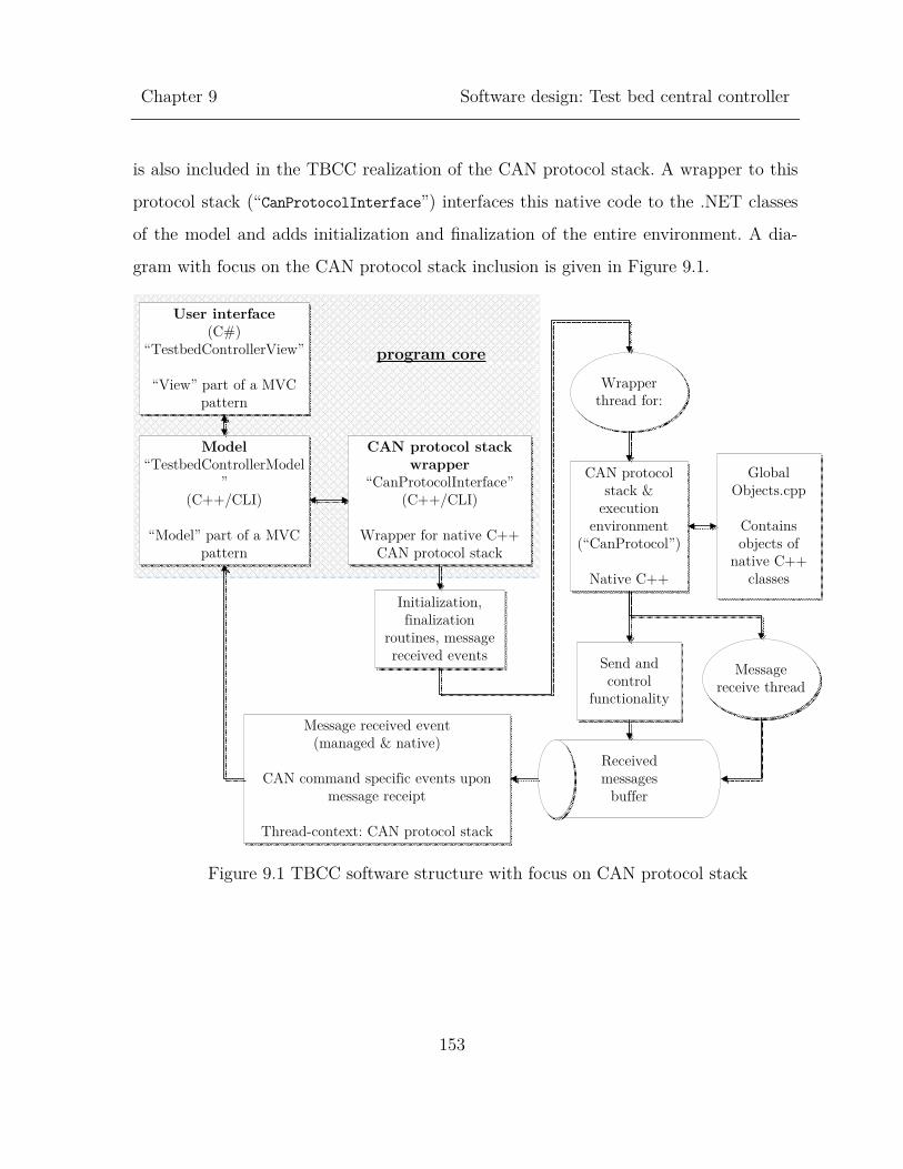
Chapter 9
Software design: Test bed central controller
153
is also included in the TBCC realization of the CAN protocol stack. A wrapper to this
protocol stack (“CanProtocolInterface”) interfaces this native code to the .NET classes
of the model and adds initialization and finalization of the entire environment. A dia-
gram with focus on the CAN protocol stack inclusion is given in Figure 9.1.
Figure 9.1 TBCC software structure with focus on CAN protocol stack
program core
CAN protocol stack &
execution environment
(“CanProtocol”)
Native C++
Send and control
functionality
Message receive thread
CAN protocol stack wrapper
“CanProtocolInterface”(C++/CLI)
Wrapper for native C++ CAN protocol stack
Wrapper thread for:
Initialization, finalization
routines, message received events
Model“TestbedControllerModel
”(C++/CLI)
“Model” part of a MVC pattern
User interface(C#)
“TestbedControllerView”
“View” part of a MVC pattern
Received messages
buffer
Message received event(managed & native)
CAN command specific events upon message receipt
Thread-context: CAN protocol stack
GlobalObjects.cpp
Contains objects of
native C++ classes

Chapter 9
Software design: Test bed central controller
154
9.3.3 Threading model
Using multiple threads for a user interface (UI) application can have the advantage that
the user interface does not freeze during long computations on program data. It can also
improve reaction speed for such long computations, if this is required.
Since the CAN protocol stack requires its own thread anyway, the TBCC software
already comes with two threads: the user interface thread (default) and the CAN proto-
col stack. Aside from other local and independent computations in separate threads,
these are the only program-defined threads in this software.
The user interface thread executes all the code related to user interfaces and all the
code that results from user inputs to user interfaces. Data updates from the model have
to be synchronized to the user interface thread before updating the user interface (.NET
Windows Forms requirement).
The CAN protocol stack operates around the second most common source of input
and output to the TBCC software, i.e. the communication link. It handles all messages
received by CanControl and initiates model changes and events, if required.
This has two consequences: most of the model code runs in the CAN protocol stack
code and the model has to be thread-safe for most parts.
In order to ensure thread-safe execution of the TBCC, some measures have to be taken.
To access any UI element, the code has to be executed in the same thread that created
that element. For this reason, all accesses to UI elements are passed through the UI
thread’s message queue to be executed by this thread using .NET delegates (by the
UIThread extension method). In the model, critical sections (Monitor, locks) are heavily
used to serialize multiple access to the Model. Where data is not to be reused, data
copies are created before a thread-context switch is performed to avoid multiple same-

Chapter 9
Software design: Test bed central controller
155
time access to the same data base that could potentially result in data corruption oth-
erwise. Queues can also be used to move data between threads. This is used between the
CAN protocol stack thread and a thread used to read CAN messages from the USB-
CAN adapter (inside CanControl).
9.4 Implementation overview: Model
A block structure of the model is shown in Figure 9.2. Its components are discussed in
the following sections.
Figure 9.2 TBCC ‘model’ block structure

Chapter 9
Software design: Test bed central controller
156
9.4.1 CAN communication
CAN communication is realized as outlined in Figure 9.1 based on the CAN protocol
stack written in C++. CAN messages can be created and consumed in any component
of the model, but are not accessible by the view. Any data changes resulting from CAN
communication can trigger events that the view listens to. The CAN protocol was de-
signed to ensure that any communication results in a state-less TBCC software or low
number of states necessary in the TBCC, so that during a connection loss no undefined
states can occur. When a (re-) connection happens, all states present have to be syn-
chronized with the current states in the respective SMCU. The SMCU states have pri-
ority over any states known to the TBCC. States that have to be synchronized are the
current operation controller state, for example.
9.4.2 MicrogridModule, SimulationModule, DcBusModule
A model representation of simulation modules and DC-bus voltage controller modules is
realized in the classes MicrogridModule, SimulationModule and DcBusModule.
MicrogridModule contains all code representing functionality that is common to both
module types: Operation control (start/stop, emergency shutdown and status), protec-
tion system control and local measurements. Most of this functionality is a code interface
to the SMCU functionality, provided through the CAN communication link.
SimulationModule is a class derived from MicrogridModule and adds simulation module
specific functionality: grid interfacing control loops, plant models and the profile ser-
vice20.
20 See section 9.4.7

Chapter 9
Software design: Test bed central controller
157
DcBusModule is also derived from MicrogridModule, but only adds minor functionality.
9.4.3 Microgrid module management
All modules online or inactive are listed in MicrogridModuleManagement until manually
remove from this list. All modules that have been seen on the CAN bus at least once
during the current TBCC runtime are either online or inactive. Modules that are not
online and have never been detected on the CAN bus during the current TBCC runtime
are not listed.
MicrogridModuleManagement provides dynamic access to all MicrogridModules available
and notifies model and view components about changes in the list.
9.4.4 Grid interfacing control loops
All grid interfacing control loops are parameterized using a standardized set of floating
point parameters (35 parameters). An abstract base class, ControlLoopModel, allows stor-
ing, updating, setting and getting these parameters using a dictionary class. Data change
events are provided for other model and view components. Specific control loop imple-
mentations (derived from ControlLoopModel), such as the ControlLoopModelVsBasedDroop,
only have to define which of the 35 parameters are used for this control topology. Every
other functionality is available through the base class ControlLoopModel.
Please note that all parameter names (must) have matching naming with profile ser-
vice commands (see section 9.4.7).

Chapter 9
Software design: Test bed central controller
158
9.4.5 Plant models
Similarly to ControlLoopModel, an abstract plant model class PlantModel exists. It sup-
ports storing, updating, setting and getting a set of floating point parameters, as well.
However, there is no pre-defined number of parameters. This is, because different plant
models cannot be standardized as much as different grid interface control topologies. For
this reason, derived classes representing an actual plant model implementation (Plant-
ModelPV, for example) must define all possible parameters that are to be handled by
PlantModel. If plant models have internal variables that can be valuable as a measure-
ment signal (for example, the DC-bus voltage in a PV plant software model), these
measurement signals have to be made available using the measurements system de-
scribed next. PlantModel does not offer any functionality for this.
Please note that all parameter names must have matching naming with profile service
commands (see section 9.4.7).
9.4.6 Measurements
Certain variables in a DC-bus voltage controller module or simulation module can be of
interest on a continuous basis. Mostly, these are local measurements by the Microgrid
module (voltages, currents, power, temperature…). Also, variables inside plant models
can be of interest, as mentioned before.
All these ‘measurements’ can be transported to the TBCC through CAN for recording
in RAM and/or disk, plotting and later analysis. Each MicrogridModule has an object of
class MeasurementsRecorder. This class keeps track of all measurements that a
MicrogridModule is currently subscribed to. Each single measurement is represented by a
MeasurementStream. These MeasurementStreams record received data in RAM by default

Chapter 9
Software design: Test bed central controller
159
and write it to disk in batches, if activated. MeasurementStream is the class that communi-
cates through CAN, while MeasurementsRecorder itself does not. Every MeasurementStream
can receive measurements at the rate of 1 Hz, 10 Hz, 100 Hz or 1 kHz. It is possible to
transmit up to about 9 single value measurements at 1 kHz over the CAN bus simulta-
neously. However, at exceedingly high constant CAN bus load, some measurements are
deactivated automatically in order to not overload the CAN bus.
9.4.7 Profile service, command file execution
One important component of a Simulation Controller role is to define the environment
for a simulation scenario. Environment can be expressed as weather, load, irradiation,
wind speed and direction, temperature and other factors that vary over time. It is im-
practical to change all these parameters by hand at the right time in order to replicate
a correct profile of these parameters with the correct slope.
For this reason, the ProfileService defines an automatic execution of commands (Pro-
fileCommand) based on an artificial simulation time managed by SimulationTimer. All
ProfileCommands can be loaded from a file with a defined file format based on comma-
separated values. The execution of commands is accurate down to one second of simu-
lation time and 0.1 second of simulation time for programmable ramping of values.
The SimulationTimer allows the creation of an artificial time for the entire experiment.
The timer can be started, paused and reset. The timer speed can be adjusted, so that
an experiment does not have to take as long as the time it is supposed to represent.
Each MeasurementStream also records the simulation time so that plotting and analysis is
possible against real time and simulation time.

Chapter 9
Software design: Test bed central controller
160
ProfileCommands can be executed by four components: MicrogridModules,
ControlLoopModel, PlantModel and MeasurementRecorder to change internal state. Control
loop and plant model configuration by the TBCC view generates ProfileCommands in
order to change a matching parameter. ProfileCommand and configuration parameter are
matched by their string name representation. For this reason, parameter names in con-
trol loop topologies/plant models must match the ProfileCommand name definition for
each of these.
9.4.8 Global simulation controller
The GlobalSimulationController groups all ProfileService objects (each
SimulationModule has one) and provides global control over the automatic execution of
timed commands. The automatic execution is expressed by five states (Figure 9.3): (1)
simulation inactive, (2) simulation start preparation, (3) simulation active, (4) simula-
tion paused and (5) simulation shutdown.
Figure 9.3 States of global simulation control
(1) is the default state in which no action is taken. As soon as all profiles and the
simulation time is set up, the global simulation can be started which triggers a change
to state (2). In state (2), all modules are prepared for simulation. For each participating
simulation module, a set of PreparationCommands (special ProfileCommands for simulation

Chapter 9
Software design: Test bed central controller
161
preparation) can be defined that bring this simulation module into the desired state
before simulation starts. For simulation modules, this has to include the command to
start up the converter. DC-bus voltage controller module(s) are started automatically
and no ProfileCommands or PreparationCommands can be executed on them. The initializa-
tion happens for all participating modules in a serial manner, which can be defined prior
to global simulation start. In case of an emergency shutdown, the global simulation can
be aborted. State (3) represents a running simulation. During this state, the
SimulationTimer starts at its initial time with configured speed. All ProfileServices listen
to this SimulationTimer time and execute commands at the execution time defined in
each ProfileCommand. At any time during a running simulation, it is possible to pause a
simulation (4), which means that the SimulationTimer is paused. The current state of
the test bed is preserved. Finally, during simulation shutdown (5), all modules are shut
down in reversed preparation order.
GlobalSimulationControl controls the operation of SimulationTimer.
9.4.9 Logging
Using NLog21, logging capabilities are available to all program modules in model and
view. Logging can be used for debugging and event tracing. Logging information is saved
to the application folder and visualized in text fields within the application. It is possible
to set filters to determine the grade of severity of logging information to be logged, such
as ‘debug’, ‘info’, ‘warn’, ‘error’ and ‘fatal’.
21 http://www.nlog-project.org

Chapter 9
Software design: Test bed central controller
162
9.5 Implementation overview: View
This section briefly describes the ‘view’ part of the TBCC software that is completely
implemented in C#. A block structure is shown in Figure 9.4. Screenshots of main user
interface components are given in appendix C.3.
Figure 9.4 TBCC ‘view’ block structure
9.5.1 Main window
The main window serves as host window to many data displays that are mostly pro-
grammed in external components (“user controls”). These user controls can be added to
the main window in tabs as needed. Common user controls are for user interface (UI)
representation of the global simulation control, measurements, DC-bus voltage controller
module(s) and simulation modules. The view does not manage any program states nor

Chapter 9
Software design: Test bed central controller
163
does it hold core information. It rather takes all information from the model and trans-
forms it into a form required for display to the user. The view is as low in states as
possible. The interface to the model is realized through event listeners (.NET delegates)
for data flow from model to view and as model method calls for data flow from view to
model.
As simulation modules and DC-bus voltage controller module are detected on the
(activated) CAN bus, more and more tabs for these modules are added right to the “App
log” tab.
9.5.2 SimulationModule, DcBusModule, control loops, plant
models
Each simulation module and DC-bus voltage controller module is represented by a
SimulationModuleUI and DcBusModuleUI, respectively. The SimulationModuleUI allows the
control of:
Simulation module operational state and protection system
Profile commands to be applied to this module and activation for global simu-
lation control
Grid interfacing control loop configuration
Plant model configuration
Selection of a set of compatible grid interfacing control loops and plant models
Log output for this module
The DcBusModuleUI allows the control of:

Chapter 9
Software design: Test bed central controller
164
DC-bus voltage controller module operational state and protection system
Activation for global simulation control
Log output for this module
9.5.3 Measurements, plotting
Another user control summarizes all MeasurementsRecorders and MeasurementStreams of
all MicrogridModules in one UI. It allows controlling the measurements taken and the
folder for recordings on the hard disk. Each of the active measurements can be displayed
in plots with real-time updates.
9.5.4 Global simulation control
The GlobalSimulationControlUI heavily interfaces with GlobalSimulationControl (model
component) and exposes all of GlobalSimulationControl’s functionalities to the user. It
also allows to control the simulation time.
9.6 Interfacing a secondary controller algorithm
In this thesis, no elements of a Microgrid central controller (for secondary or tertiary
control) have been implemented. However, through the TBCC model, all necessary in-
formation is available:
Available sensor data of all modules can be obtained using Measurements Recorders
Any supported action, such as setting droop controller set-points can be per-
formed by invoking the appropriate methods in the TBCC model.

Chapter 9
Software design: Test bed central controller
165
For example, in order to change the droop controller set-points of a specific simulation
module, the droop controller parameters of a simulation module’s ControlLoopModel (spe-
cifically: ControlLoopModelVsBasedDroop) have to be changed in the ControlLoop field of
that simulation module. These changes will be communicated through CAN and will be
applied to the SMCU firmware.
9.7 Summary
The test bed central controller (TBCC) is a Windows Desktop application that realizes
the role as a simulation controller and provides interfaces for a future Microgrid central
controller. It provides a human machine interface to all significant functionalities of the
DC-bus voltage controller module and simulation modules. It allows recording any avail-
able sensor measurement to RAM, disk and/or plots and to automate all available func-
tionalities using script files on an artificial time base. The TBCC software structure has
been highlighted, especially in Figure 9.1, Figure 9.2 and Figure 9.4. With this overview
and knowledge about the design principles applied, assessment and in-depth work with
the source code should be fast and simple.

Chapter 10
Experimental results
166
Chapter 10
Experimental results
This chapter presents measurements taken from the implemented test bed. Different
testing scenarios demonstrate the proper functionality of individual components and of
the entire test bed. For this reason, the first tests demonstrate functionality of individual
grid-interfacing control loops and plant models. After that, measurements from the DC-
bus voltage controller module are presented. This chapter concludes with experimental
recordings from a scenario comparable to the one described in Chapter 7 running an
islanded grid with load, storages and photovoltaic plant on a 24 hour profile.
Please note: if not stated differently, all power flows given in this chapter for simulation
modules are positive when power flows from the simulation module to the Microgrid
bus. This means, that a load to the grid has a dominantly negative power flow.
10.1 Grid-following converter
The grid following converter provides the ability to absorb or inject active and/or reac-
tive power from/to an existing grid. For that, a stable voltage and frequency has to be
present. The grid-following converter has been tested when connected to the laboratory
electricity grid in order to demonstrate maximum dynamic performance, as shown in
Figure 10.1. During the development, it has been found that the voltage-source based

Chapter 10
Experimental results
167
droop controller topology is unable to maintain a stable grid voltage22 during the most
extreme transients caused by the fast reaction of the grid-following converter. For stable
operation with the voltage-source based droop controller, the grid-following converter’s
current controller integral gain has been slightly reduced.
Figure 10.1 Grid-following converter test configuration
To verify stable and high-quality performance, the grid-following converter has been
tested at steady state with power references in all four quadrants for 0%, 25%, 50% and
100% load (Figure 10.3). After that, the dynamic performance has been tested through
an active power reference step from 0% to 100% rating (Figure 10.2).
In these recordings, it can be seen that the grid-following control topology is able to
generate high quality current waveforms for the entire operating range. Some high-fre-
quency harmonics can be noted in the transformer currents (green). The frequency
matches the power filter resonance frequency quite well, indicating small system reso-
nances in the grid connection. In the filter inductor currents (ᵅ�����), which are directly
controlled by a current controller, the resonances are not apparent. The difference be-
tween transformer and inductor currents in all measurements is caused by the filter
capacitor reactive power contribution. This becomes most apparent in the first graph in
Figure 10.3. The red capacitor voltage waveform is very noisy due to the measurement
22 Here, ‘not stable’ means that the test bed’s protection system is activated due to short-term tran-
sients

Chapter 10
Experimental results
168
setup. The location of the measurement points was very close to the filter inductors that
are a major source of EMI emissions.
Figure 10.2 proves a fast dynamic performance of the grid-following controller. It is
able to follow a step response within 1-2ms.
Figure 10.2 Grid-following control topology: transient performance
(active power reference step change from 0W to 5000W). Green: transformer cur-
rent (10A/div); Yellow: filter inductor current (10A/div); red: filter capacitor voltage
(200V/div). All graphs show phase A. Time scales: (a) 5ms/div; (b) 50ms/div

Chapter 10
Experimental results
169
Figure 10.3 Grid-following control topology: steady state, four quadrant perfor-
mance.
Green: transformer current (10A/div); Yellow: filter inductor current (10A/div);
red: filter capacitor voltage (200V/div). All graphs show phase A.

Chapter 10
Experimental results
170
10.2 Grid-supporting converter
10.2.1 Voltage-source based droop controller
The voltage-source based droop controller can be used to realize the grid-former and the
grid-supporting converter roles. Its main functionality is to define a stable grid voltage
and frequency, stand-alone or in cooperation with other grid-supporting converters. Up
to its power rating, it has to be able to keep the grid voltage at a stable level and the
voltage waveform’s harmonic contents low. The generation of balanced voltages is highly
desired.
In order to demonstrate the performance of the implemented voltage-source based
droop controller, the following three test cases have been run on the Microgrid test bed:
1. One simulation module with voltage-source based droop controller as grid in-
terface together with one simulation module using the ZIP load and grid-fol-
lowing converter. A time-varying load is applied.
2. Two simulation modules with voltage-source based droop controllers as grid
interfaces together with one simulation module using the ZIP load and grid-
following converter. A time-varying load is applied.
3. One simulation module with voltage-source based droop controller as grid in-
terface and no other connected simulation modules. The negative sequence con-
trol loop is activated and deactivated to demonstrate its functionality.
a. Test case 1: Single droop controller with load connected
To show that the voltage-source based droop controller is able to define a good voltage
waveform under typical loading conditions, a load was operated with power references

Chapter 10
Experimental results
171
as given in Table 10.1. Based on the given load profile, Figure 10.4 shows transformer
currents and dynamic response of the voltage-source based droop controller. In Figure
10.6(a)-(d) it can be seen that the droop controller module is able to maintain steady
voltage levels, varies voltages w.r.t. the reactive power demand and supplies any load
demand present within its limits. Any differences between supplied and consumed power
are due to the two transformers that are between both simulation modules, as well as
inrush current limiters in AC breaker boxes that initially consume more energy in order
to heat up after an increase in power flow. The inrush current limiters cause a change of
power injection of the droop controlled module during load power steady-state, as can
be seen in Figure 10.6(c) during seconds four to eight.
The system frequency has been determined using the load module PLL. This PLL
introduces strong transient oscillations for a few seconds, as can be seen. However, the
level the detected frequency converges to, becomes apparent, which corresponds to the
expectations of droop control. After second 12, the load module was turned off and
disconnected. Therefore the system frequency variable remains in an undefined state
after second 12.
A difference compared to the simulated case in section 5.3.4 is that the maximum load
power is 4kVA instead of 5kVA. The reason for this is, that transformer magnetization
losses and reactive power consumption cause the droop controlled module to supply
more complex power than the load module consumes. A load power of 5kVA would
exceed the simulation module ratings and cause a voltage collapse.

Chapter 10
Experimental results
172
Table 10.1 Load power references for test case 1
Time [s] Complex power reference [VA] Power factor reference
0 0 1
2 2000 1
4 4000 1
6 4000 0.9
8 2000 0.9
10 0 0.9
Figure 10.4 (a) ᵅ����� for droop controlled module during load profile defined for test
case 1.
During the last segment, the load was turned off and disconnected. Currents:
10A/div; time: 2.5s/div. (b) ᵅ����� for droop controlled module during a load step from
0W to 2500W. Currents: 10A/div; time: 25ms/div
b. Test case 2: Two droop controllers with load connected
When droop controllers operate in parallel, the power droop scheme is supposed to
determine short-term active and reactive power sharing in order to provide a stable local

Chapter 10
Experimental results
173
voltage and frequency. In this experiment, a load profile with 2.5 kVA and 5 kVA step
changes has been used, instead of 2 kVA and 4 kVA before (Table 10.1). This became
possible through the addition of a second droop module so that enough capacity is
available to supply the load and losses. Figure 10.6(e)-(h) shows power flows and voltages
for this test case and demonstrates that a decentralized and fast power sharing is ac-
complished. The average between all three phases of the capacitor voltages of a module
is displayed, so that the overall voltage levels, instead of voltage imbalances, become
apparent. To the droop controller, the overall voltage levels are of interest, only. In the
aforementioned figure, it can be seen that the droop module voltages remain fairly con-
stant during active power-only operation and deviate as soon as a reactive power com-
mand is added. The load module was turned off and disconnected at second 12, so that
displayed voltage and frequency measurements for after that are invalid for this module.
The frequency was detected using the load module PLL, so that previous comments on
frequency transients apply. Figure 10.5(a) shows transformer currents of one droop mod-
ule during the load cycle, confirming the module dynamics and current/power injection
levels.
Figure 10.5(b) shows the voltages produced by droop module 2 during a load step
change from 0W to 5000W. There, it can be seen that the droop controllers are capable
of restoring the voltage to nominal levels within about four to seven cycles.

Chapter 10
Experimental results
174
Figure 10.5 Two voltage-source droop controlled modules in operation.
(a) Droop module 2 transformer currents, phase A (yellow) and B (green). Cur-
rents: 10A/div; time: 2.5/div. (b) Droop module 2 capacitor line-to-line voltages (ᵅ�����:
yellow, ᵅ�����: green, ᵅ�����: blue) and phase A transformer current (red) during load
module step change from 0W to 5000W. Voltages: 100V/div; currents: 10A/div; time:
20ms/div

Chapter 10
Experimental results
175
Figure 10.6 (a)-(d): test case 1. (e)-(h): test case 2

Chapter 10
Experimental results
176
c. Negative-sequence controller for balanced voltages
Due to unbalanced loading of the voltage-source based droop controller (for example,
due to unbalanced, non-linear transformer magnetization currents), the module’s capac-
itor voltages can become highly unbalanced and as a result, the Microgrid voltages are
unbalanced, as well.
Without the negative-sequence control loop extension (NSCL), a simulation module
with a voltage-source based control topology at no load typically produces unbalanced
Microgrid bus voltages. By measurement, these Microgrid bus phase-to-neutral RMS
voltages have been determined (NSCL off NSCL on) :
Phase A: 121.5V 119.1V
Phase B: 120.4V 119.1V
Phase C: 115.1V 118.8V
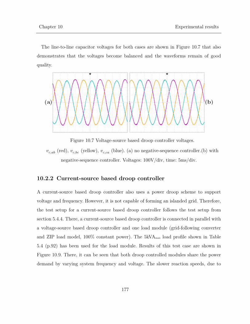
Chapter 10
Experimental results
177
The line-to-line capacitor voltages for both cases are shown in Figure 10.7 that also
demonstrates that the voltages become balanced and the waveforms remain of good
quality.
Figure 10.7 Voltage-source based droop controller voltages.
ᵅ����� (red), ᵅ����� (yellow), ᵅ����� (blue). (a) no negative-sequence controller.(b) with
negative-sequence controller. Voltages: 100V/div, time: 5ms/div.
10.2.2 Current-source based droop controller
A current-source based droop controller also uses a power droop scheme to support
voltage and frequency. However, it is not capable of forming an islanded grid. Therefore,
the test setup for a current-source based droop controller follows the test setup from
section 5.4.4. There, a current-source based droop controller is connected in parallel with
a voltage-source based droop controller and one load module (grid-following converter
and ZIP load model, 100% constant power). The 5kVAmax load profile shown in Table
5.4 (p.92) has been used for the load module. Results of this test case are shown in
Figure 10.9. There, it can be seen that both droop controlled modules share the power
demand by varying system frequency and voltage. The slower reaction speeds, due to

Chapter 10
Experimental results
178
voltage and frequency filtering in the current-source based droop control topology, in-
troduce short term power oscillations between both droop controllers upon fast load
changes. These transients are stronger than in the case of two paralleled voltage-source
based droop controllers. Some additional high-frequency oscillations during second 4 and
8 (Figure 10.9) are introduced, because the load module operates at its maximum output
power and power limiting algorithms are activated. These algorithms determine the
maximum current to be injected based on the system voltage. Any noise in the detected
system voltage amplifies noise in the power limit set-points. Figure 10.8 shows the trans-
former currents that the voltage-source based droop controller injects into the system
during the load profiles. The current transients after a load change are clearly visible.
Figure 10.8 : ᵅ����� for voltage-source based droop controlled module during load
profile defined for test case 1.
During the last segment, the load was turned off and disconnected. Currents:
10A/div; time: 2.5s/div.

Chapter 10
Experimental results
179
Figure 10.9 System voltage (a), frequency (b) and power flow (c)-(d) in a current-
source based droop and voltage-source based droop controlled islanded test grid

Chapter 10
Experimental results
180
10.3 Load plant model
The load plant model generates power references for a grid-following converter based on
a nominal power and the connection voltage. It allows to imitate a combination of con-
stant-impedance, constant-current and constant-power loads that are balanced, three-
phase linear loads.
To test the proper functionality of this model, a voltage-source based droop controller
has been used to form a grid to which the load module was connected. The voltage and
frequency droop scheme was deactivated so that a constant voltage and frequency have
been maintained. The reference voltage changed between 120V and 100V every 5 seconds
to see the response of the load module to it.
The load module configuration changed over time according to Table 10.2.
Table 10.2 ZIP load configuration for presented test case
Time [s] ZIP load configuration P0;Q0
0…12 100% constant power ᵃ�� = 2500ᵃ�;ᵃ�� = 0ᵃ�ᵃ�ᵅ�
12…22 100% constant current ᵃ�� = 2500ᵃ�;ᵃ�� = 0ᵃ�ᵃ�ᵅ�
22…32 100% constant impedance ᵃ�� = 2500ᵃ�;ᵃ�� = 0ᵃ�ᵃ�ᵅ�
32…42 100% constant power ᵃ�� = 0ᵃ�;ᵃ�� = 2500ᵃ�ᵃ�ᵅ�
42…52 100% constant current ᵃ�� = 0ᵃ�;ᵃ�� = 2500ᵃ�ᵃ�ᵅ�
52…70 100% constant impedance ᵃ�� = 0ᵃ�;ᵃ�� = 2500ᵃ�ᵃ�ᵅ�
Figure 10.10 presents recordings from the described test case. It can be seen that
despite local voltage variations caused by the connection transformers, the ZIP load

Chapter 10
Experimental results
181
module is able to operate with constant power, constant current and constant imped-
ance, even under severely changing connection voltages. This holds for both active and
reactive power.
Figure 10.10 Load plant model performance.
Module voltages (a), load module power (b), current (c) and output impedance (d)
during constant-power, constant-current and constant-impedance operation for active
and reactive power

Chapter 10
Experimental results
182
10.4 Photovoltaic plant model
The photovoltaic plant model is a software model executed at real-time and linked to
the converter hardware using the HIL interface definition. To demonstrate the internal
performance of the photovoltaic plant, a test setup with two simulation modules has
been used. One simulation module defines the grid frequency and voltage using the
voltage-source based droop controller and the other module uses a grid-following control
topology together with the PV plant model. Key parameters of the PV model are listed
in Table 10.3. These parameters correspond to the default configuration for this plant
model. Measurement results for two test cases are presented here:
Case 1: Normal operation with steps in the solar insolation values
Case 2: Operation with PV curtailment in effect
Table 10.3 PV model key parameters
Parameter Value
PV array: 4x4 CanadianSolar CS6X-P 315Wpeak
Maximum PV array output at standard light intensity 5040W
Nominal virtual DC-bus voltage 400V
Upper DC-bus voltage threshold for PV curtailment 430V
Lower DC-bus voltage threshold for grid interface curtailment 370V
Assumed VSI efficiency 95%
10.4.1 Normal PV model operation
To demonstrate feasible PV array and MPPT tracker operation, Figure 10.11 shows the
response of the PV array system to a solar insolation step change from 50 ᵃ�/ᵅ�� to

Chapter 10
Experimental results
183
300 ᵃ�/ᵅ��. It can be seen that MPPT tracker and converter adjust quickly to the
changed input and operate steadily at the new operating point. The virtual DC-bus
voltage is quickly regulated to its nominal value after the solar insolation step change
by the virtual DC bus control loop in the HIL grid interface component.
Figure 10.12 shows a similar scenario and demonstrates, that the actual injected active
power in the Microgrid follows the model variables well. A larger drop in the virtual DC-
bus voltage occurs when the solar insolation drops back to 50 ᵃ�/ᵅ�� because the mini-
mum allowed AC output power was set to 0W. This takes away means from the virtual
DC bus controller for fast voltage restoration at low output power.
Figure 10.11 PV plant model variables at a solar insolation step change from
50 ᵃ�/ᵅ�� to 300 ᵃ�/ᵅ��.
PV array voltage (a), PV array output current (b), Virtual DC bus voltage (c) and
PV array output power (d). Total time: 20 seconds, based on graphs (a) and (c).
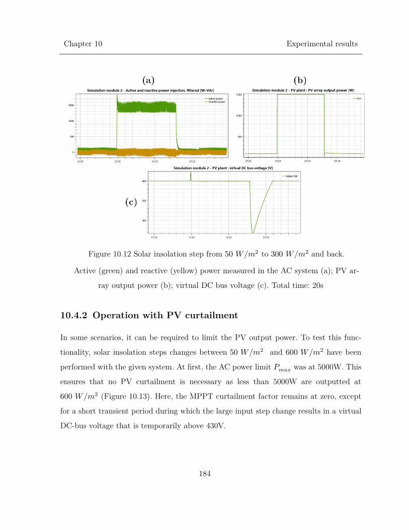
Chapter 10
Experimental results
184
Figure 10.12 Solar insolation step from 50 ᵃ�/ᵅ�� to 300 ᵃ�/ᵅ�� and back.
Active (green) and reactive (yellow) power measured in the AC system (a); PV ar-
ray output power (b); virtual DC bus voltage (c). Total time: 20s
10.4.2 Operation with PV curtailment
In some scenarios, it can be required to limit the PV output power. To test this func-
tionality, solar insolation steps changes between 50 ᵃ�/ᵅ�� and 600 ᵃ�/ᵅ�� have been
performed with the given system. At first, the AC power limit ᵃ���� was at 5000W. This
ensures that no PV curtailment is necessary as less than 5000W are outputted at
600 ᵃ�/ᵅ�� (Figure 10.13). Here, the MPPT curtailment factor remains at zero, except
for a short transient period during which the large input step change results in a virtual
DC-bus voltage that is temporarily above 430V.

Chapter 10
Experimental results
185
After that, ᵃ���� has been set to 2000W (Figure 10.14). This could mimic an inverter
sized smaller than the maximum available PV output. As a result, PV power curtailment
is necessary to keep the AC output power at 2000W or below. During the phase of
600 ᵃ�/ᵅ�� insolation, the PV curtailment factor becomes non-zero, which means that
the PV module voltage is increased beyond its MPP voltage to reduce PV array power
output. A PV curtailment factor of 0.02 means, that the current PV array reference
voltage is increased by 2% of the PV array open-circuit voltage, compared to the last
voltage reference when under MPPT operation. Accordingly, the AC system active power
is limited to about 2000W on average23. As soon as the solar insolation reduces to
50 ᵃ�/ᵅ�� again, the PV curtailment factor returns to zero, which means that MPPT
operation is resumed.
The wide noise band of injected AC power results from unbalanced and non-linear
transformer magnetization currents of the simulation module interfacing transformer.
23 The accuracy of power limiters requires some future work, as the injected active power is slightly
above 2000W. This is functionality is realized in the grid-interfacing control loops and not the PV model.

Chapter 10
Experimental results
186
Figure 10.13 Solar insolation step change from 50 ᵃ�/ᵅ�� to 600 ᵃ�/ᵅ�� and back.
ᵃ���� = 5000ᵃ� .
No PV curtailment. Active and reactive power into grid (a); MPPT curtailment
factor (b); virtual DC bus voltage (c); PV array output (d). Total time displayed: 20s

Chapter 10
Experimental results
187
Figure 10.14 Solar insolation step change from 50 ᵃ�/ᵅ�� to 600 ᵃ�/ᵅ�� and back.
ᵃ���� = 2000ᵃ� .
Hence, PV curtailment is in effect. Active and reactive power into grid (a); MPPT
curtailment factor (b); virtual DC bus voltage (c); PV array output (d). Total time
displayed: 20s.
10.5 DC-bus voltage controller module
The DC-bus voltage controller module’s primary objective is to control the test bed’s
DC-bus voltage to 450V. In order to do so, it connects to the laboratory’s electricity
grid to exchange up to 5kW of power. To demonstrate the proper operation of this
module, the test setup of Figure 10.1 was used again. In this case, the grid-following
converter presented a load to the DC bus.

Chapter 10
Experimental results
188
Using this configuration, measurements showing the DC-bus voltage quality and reg-
ulation are presented. Additionally, a startup and shut down cycle is presented.
In Figure 10.15 it can be seen that the DC-bus voltage ripples remain below
2ᵃ�����−���� under all loading conditions in this test setup. This corresponds to a maxi-
mum ripple of 0.44%ᵃ������� and can be considered sufficient for simulation modules.
During changing DC bus loading conditions, the DC-bus voltage naturally deviates
more. To test this, a load power step change from 0W to 5000W was performed. This
means, that the load module injects about 5000W into the DC bus leading to a tempo-
rary rise of the DC-bus voltage. The result in Figure 10.16 shows that the DC-bus
voltage controller module is capable of restoring the DC-bus voltage to its normal value
within about 10ms. The voltage deviation clearly remains within the defined permissible
protection range24 without triggering any protection action. The voltage deviation is
about 2.3%ᵃ�������, thus still reasonable for a temporary event.
Figure 10.17 shows a full cycle of the DC-bus voltage controller module, including
startup, normal operation (unloaded) and shutdown.
24 410V…490V as defined in appendix A.4.1

Chapter 10
Experimental results
189
Figure 10.15 DC-bus voltage ripples under different loading conditions.
ᵃ��� = 450ᵃ� . Voltage resolution: 1V/div. Time: 5ms/div

Chapter 10
Experimental results
190
Figure 10.16 DC-bus voltage (blue) during load power step change (0W to 5000W).
Yellow: DC current into DC-bus voltage controller module. Voltage: 5V/div, cur-
rent: 10A/div, time: 20ms/div.
Figure 10.17 DC-bus voltage during full operating cycle:
Off, slow capacitor charging through diode rectifier mode of operation, PWM-
based ᵃ��� linear ramp-up, normal operation at 450V, PWM-based ᵃ��� linear ramp-
down, slow capacitor discharging and off. Voltage: 100V/div, time: 2s/div

Chapter 10
Experimental results
191
10.6 Simulation of a 24-hour grid scenario on the test
bed
The final test case presented in this thesis combines all components into one experiment.
The case that was simulated in Chapter 7 has been reproduced on the implemented test
bed. All input parameters and module configurations were the same, except for the
storage module droop gains25. TPS-files26 have been created, so that module configura-
tion, measurements collection, solar insolation and load profile were set automatically.
The simulation has been executed with 20x real-time speed, so that a 24 hour profile
was completed in 72 minutes. All measurements were recorded by hardware and software
created in this thesis. MATLAB was used to plot the measurements taken.
The overall results are shown in Figure 10.18. There, the active and reactive power
flows resemble the behavior of all four modules with their characteristic role. The pho-
tovoltaic plant injects active power dependent on the current solar insolation. The load
plant withdraws power according to its load profile at power factor 0.9. The two storage
modules compensate for any power differences and power losses in the system (for ex-
ample, transformer magnetization). As the PV plant was configured to operate at unity
power factor, it does not supply any reactive power to the load demand. Only the storage
modules have to supply this demand. Accordingly, the voltage level shows significantly
less change due to the PV active power output variations than the system frequency.
25 Large storage module: 0.00003 for P/f droop; 0.0001 for Q/V droop. Small storage module: 0.00004
for P/f droop; 0.0002 for Q/V droop. 26 The TPS file format describes ProfileCommands in a file that can be used by
GlobalSimulationControl

Chapter 10
Experimental results
192
However, the fact that there is some change indicates a coupling between the active and
reactive power droops due to a finite X/R ratio of the AC system.
Figure 10.18 24-hour simulation: power flows.
Active (a) and reactive (b) power; and system frequency (c) and voltages (d). Posi-
tive power: generation, negative power: consumption

Chapter 10
Experimental results
193
Key internal variables from the photovoltaic plant are shown in Figure 10.19. The
virtual DC-bus voltage remains at its nominal value starting after the moment when the
solar irradiation becomes greater than 0 ᵃ� /ᵅ�� and the PV plant DC bus has been
charged (see Figure 10.20 for more details). After 8:00pm, the sun has set and PV output
power reaches zero. This deactivates the PV model computation27. The MPPT tracker
and converter adjust the PV array voltage continuously in order to extract maximum
power at all times when the solar insolation is above 0 ᵃ� /ᵅ��.
Figure 10.19 24-hour simulation: PV plant variables
27 The DC-bus voltage remains at about 400V after 8:00pm, because no shutdown
mechanism or capacitor self-discharge process has been modeled.

Chapter 10
Experimental results
194
Figure 10.20 24-hour simulation: PV plant DC-bus voltage (zoom)
Based on the storage module capacities of 20 kWh and 10 kWh, their SOC changes
during the course of the day (Figure 10.21). Until the PV plant provides enough active
power to the grid, both storage modules are discharged to supply energy to the load and
feed all network losses. The PV plant rapidly charges both storages in the middle of the
day; however, it is necessary to balance out fluctuations around 10:00am and 4:00pm
where the load demand is temporarily higher than the supply of energy by the PV plant.
Compared to the simulation in Chapter 7, the SOC falls lower in the experiment. The
reason for this is the transformer magnetization losses that are at about 150W per sim-
ulation module.
Figure 10.21 24-hour simulation: storage module SOC during the day

Chapter 10
Experimental results
195
10.7 Summary
This chapter presented experimental results on a component scale and a test bed scale
to verify correct behavior of the components and the system designed. Many simulation
results presented in Chapter 5, Chapter 6 and Chapter 7 have been reproduced on the
test bed and implementation-specific aspects have been integrated into the presented
data. While some future work is necessary in detailed aspects, this chapter has demon-
strated that this test bed is capable of replicating islanded Microgrid scenarios. The
available range of variables and parameters allows the investigation of detailed questions
at the same time as bigger picture aspects. Simulating a 24 hour profile took 72 minutes
on this test bed, while a PSIM simulation of this scenario in Chapter 7 required 52
hours. Important functionalities on this test bed can be automated and more test infra-
structure can be added, so that more complex scenarios with more dynamic change over
time can easily be executed without further increase in simulation execution time.

Chapter 11
Conclusions
196
Chapter 11
Conclusions
This thesis has described the design, implementation and evaluation of a Microgrid test
bed with focus on islanded Microgrids.
In Chapter 1, the motivation for Microgrid research and the need for Microgrid test
beds have been discussed. Common test bed approaches have been reviewed. It has been
shown that, by consequently using the Hardware-in-the-loop approach, Microgrid test
beds can be realized with significantly increased flexibility at much lower costs. Derived
from this statement, a research objective has been formulated, that includes expectations
and simplifications for this thesis project.
In Chapter 2, most necessary technologies and concepts for this test bed have been
reviewed, such as the voltage-source inverter, Microgrid converter roles (grid-former,
grid-supporter and grid-feeder), followed by control concepts in the synchronous refer-
ence frame, droop control, PLLs and control of direct parallel connected three-phase,
four-leg VSIs without an AC transformer.
In Chapter 3, the research objective in Chapter 1 has been elaborated further. The
idea of a Hardware-in-the-loop Microgrid test bed has been substantiated with a more
detailed system structure and a concrete definition of requirements on all major system
components, such as voltage and power levels.

Chapter 11
Conclusions
197
Chapter 4 contains the hardware design process for a simulation module. Simulation
module components are described in terms of their functionality and design goals. A
DC-bus voltage controller module was derived from the simulation module hardware and
simulations on it have been presented, as well. For this module, the control topology has
also been discussed. This topology realizes a three-phase, power factor corrected rectifier
to control the DC-bus voltage. Information on necessary mechanical design has been
given. A cost analysis confirmed the superior cost reduction of this test bed compared
to full-scale real Microgrid test implementations.
In Chapter 5, the control loop implementations for the Microgrid converter roles ‘grid-
former’, ‘grid-supporter’ (voltage-source and current-source based) and ‘grid-feeder’ /
’grid-follower’ have been presented along with the definition of the Hardware-in-the-loop
interface for this test bed. The implementations make heavy use of control concepts in
synchronous reference frame (dq0) and include advanced concepts for unbalanced load
currents and improvements in droop control. All control loops have been formulated in
a standardized way so that the change of converter roles can be achieved easily and
quickly.
Chapter 6 dealt with the formulation and implementation of real-time software models
for plant simulation. Plants realized are a three-phase, balanced and linear ZIP load, a
comprehensive photovoltaic plant and a generic storage plant. This chapter concludes
the hardware, model and control design.
In Chapter 8 and Chapter 9, the implementation of software for a simulation module
and the test bed central controller has been discussed. Relevant design approaches and
major functionalities have been outlined to provide a good understanding of the software
developed for this test bed. All software components are designed with a high level of

Chapter 11
Conclusions
198
modularity and flexibility. This enables fast reconfiguration of this test bed to many
different test scenarios through software.
In Chapter 7, PSIM simulations of this test bed have been presented in order to define
a reference case for real test bed experiments presented in Chapter 10. The PSIM sim-
ulations took about 52 hours to simulate a test bed operation of about 20 seconds,
representing 24 hour simulation time. The experimental system operates in real time.
This strongly highlights the limitations of a computer based circuit simulation system
and the advantage of a real test bed, when the level of details and complexity is very
high.
The experimental results in Chapter 10 were presented in a similar manner as simula-
tions beforehand. The experiments have demonstrated the feasibility of this test bed
approach and outlined in details the performance each key component in this test bed
is able to achieve. The chapter closes with the demonstration of a 24 hour run of a small
islanded Microgrid.
During this thesis project a Microgrid test bed has been developed that is a valuable
tool in research and development for Microgrids and power system concepts involving
DERs. Various research concepts have already been implemented together. The feasibil-
ity and compatibility assessment of many techniques in Microgrids can easily be realized
with the current state of this test bed. This test bed can supports work on inverters for
grid applications, Microgrid control and general distribution grid management.

Chapter 12
Future work
199
Chapter 12
Future work
Various major fields of possible future work have been identified during this project:
Single-phase operation. So far, only three-phase devices have been devel-
oped and tested. However, distribution grids have a significant number of sin-
gle-phase units installed. Current simulation modules can be operated in single-
phase mode through changes in control, or single-phase simulation modules
could be developed to reduce cost per module for these modules.
Unbalanced and non-linear load currents. The current test bed mostly
assumes balanced current flows. As in real systems, load currents can be un-
balanced and contain harmonics. Various problems around the sharing of those
currents arise and have not completely been addressed in this thesis.
Distribution grid elements. The current test bed AC grid consists of a single
point of common coupling. Real distribution grids have long feeders with sig-
nificant line impedances, protection gear, capacitors, transformers, load tap
changers and different voltages and network layouts. A realistic and flexible
representation of most this gear is necessary to bring this test bed even closer
to real application cases.

Chapter 12
Future work
200
Grid connection. This test bed has been developed for islanded Microgrid
research. However, Microgrids can also be operated in grid-connected mode,
which can reveal different issues. It can be desirable to introduce a mechanism
to connect this Microgrid to a strong grid or even split the test bed in several
Microgrids. This allows to include a tertiary Microgrid control level as well.
More plant models, more grid interfaces. Significant grid participants
that are not represented in this test bed are hydro-thermal generation, internal
combustion engine based generators, wind turbines and hydroelectric plants.
Some of these plants also require a grid interface model representing electric
machines.
Secondary Microgrid control. This thesis includes an interface for second-
ary Microgrid control, but does not implement any approaches. It might be
desirable to further expand this interface and implement various secondary
control approaches.
Further minor fields of future work can be:
Inclusion of transformer-less simulation modules
Photovoltaic plants with partial shading simulation capabilities
Improvements of average Buck-Boost converter model in discontinuous conduc-
tion mode of operation
Improved sensor signal transmission (current signaling for improved noise im-
munity)
Improved power limiting capability of grid-interfacing control loops (accuracy
and dynamic performance)

201
Derivations
A.1 Virtual impedance in synchronous reference
frame for voltage-source based droop controllers
Figure A.1 depicts a single-line diagram of the CL-filter part of a three-phase VSI
with LCL filter. The capacitors are represented by the controlled voltage source ᵅ�� and
the connection impedance represents the second filter inductance L by its inductance ᵃ��
and its equivalent series resistance ᵃ��. A virtual impedance ᵃ�� = ᵃ�� + ᵅ�ᵱ�ᵃ�� is added in
series.
Figure A.1 Converter output circuit with virtual impedance
Typically, in voltage-source based droop controllers the capacitor voltage ᵅ�� is con-
trolled by a voltage control loop in synchronous reference frame receiving voltage refer-
ences of ᵅ���∗ =
√2 ᵃ������ and ᵅ���
∗ = 0. If the (virtual) voltage drop across the virtual
impedance ᵃ�� is to be accounted for, the voltage control loop has to receive references
representing ᵃ�� instead of ᵃ��. Therefore, the voltage drop across the virtual impedance
ᵅ��� is calculated in order to compute ᵅ�� = ᵅ�� − ᵅ���
.

Appendix A
Derivations
202
Assuming a system at frequency ᵱ� one can write:
ᵃ��⃗ = ᵃ��⃗ − ᵃ��⃗�− ᵃ��⃗�
(A.1)
ᵃ��⃗ = ᵃ��⃗ − ᵅ�ᵱ�ᵃ�ᵃ��⃗ − ᵃ�ᵃ��⃗ (A.2)
Defining ᵃ��⃗ = ᵃ��∠0°:
ᵃ��∠ᵰ���= ᵃ��∠0° − ᵱ�ᵃ��ᵃ��∠�ᵰ���
+ 90°� − ᵃ��ᵃ��∠ᵰ��� (A.3)
Separating into real and imaginary part:
ᵃ�ᵃ��ᵃ��⃗� = ᵃ�� − ᵱ�ᵃ��ᵃ�� cos�ᵰ���
+ 90°� − ᵃ��ᵃ�� cos�ᵰ����
ᵃ�ᵅ��ᵃ��⃗� = −ᵱ�ᵃ��ᵃ�� sin�ᵰ���+ 90°� − ᵃ��ᵃ�� sin�ᵰ���
� (A.4)
Replace 90° offsets with sin/cos function and multiply by √
2:
√2ᵃ�ᵃ��ᵃ��⃗� =
√2ᵃ�� + ᵱ�ᵃ��
√2ᵃ�� sin�ᵰ���
� − ᵃ��√
2ᵃ�� cos�ᵰ����
√2ᵃ�ᵅ��ᵃ��⃗� = −ᵱ�ᵃ��
√2ᵃ�� cos�ᵰ���
� − ᵃ��√
2ᵃ�� sin�ᵰ����
(A.5)
W.r.t selected reference angle and system frequency ᵱ�, the current ᵅ�� can be expressed
in the dq0 reference frame as follows:
ᵅ��� =√
2ᵃ�� cos�ᵰ���� (A.6)
ᵅ��� =√
2ᵃ�� sin�ᵰ���� (A.7)
ᵃ��� = 0 due to the use of Δᵃ� transformers as connection impedance in this thesis.
Also note that for the given system:
√2ᵃ�ᵃ��ᵃ��⃗� = ᵅ���
√2ᵃ�ᵅ��ᵃ��⃗� = ᵅ���
(A.8)

Appendix A
Derivations
203
Using equations (A.6), (A.7) and (A.8) in (A.5) gives:
ᵅ��� =
√2ᵃ�� + ᵱ�ᵃ�� i�� −ᵃ��ᵅ���
ᵅ��� = −ᵱ�ᵃ�� i�� −ᵃ��ᵅ��� (A.9)
ᵅ��� and ᵅ��� can be used as reference values for the voltage controller instead of
ᵅ���∗ /ᵅ���
∗ in order to implement a virtual impedance.
A.2 Virtual impedance in synchronous reference
frame for current-source based droop controllers
A grid-following converter or a current-source based grid-supporting converter control
the amount of active and reactive power injected into the grid. The exact point of power
control is typically after the filter capacitor, so that, following Figure A.1, for ᵅ��� = 0
the injected active and reactive power become:
ᵃ���� = 32
ᵅ���ᵅ��� (A.10)
ᵃ���� = −32
ᵅ���ᵅ��� (A.11)
Power consumption by ᵃ�� = ᵃ�� + ᵅ�ᵱ�ᵃ�� are usually not accounted for.
However, in order to account for the effect of a virtual impedance in a grid-following
converter based controller structure, the reference power can be adjusted accordingly.
Then, the new reference power becomes
ᵃ� ∗ = ᵃ����∗ − ᵃ���
(A.12)
ᵃ�∗ = ᵃ����∗ − ᵃ���
(A.13)

Appendix A
Derivations
204
Where ᵃ����∗ /ᵃ����
∗ are power controller references without virtual impedance and
ᵃ�∗/ᵃ�∗ are power controller references with included virtual impedance effects.
The power consumption by the virtual impedance ᵃ�� can be calculated for sinusoidal
currents based on initial power references and the current capacitor voltage in the dq0
reference frame:
ᵃ���= ᵃ��ᵃ��
� = ᵃ�� � ᵃ�∗
32 ᵅ���ᵅ���
√2�
�
(A.14)
ᵃ���= ᵱ�ᵃ��ᵃ��
� = ᵱ�ᵃ�� � ᵃ�∗
−32 ᵅ���ᵅ���
√2�
�
(A.15)
A.3 Derivation of maximum expected fundamental
VSI RMS output voltage
In order to obtain the minimum value for the VSI DC-bus voltage required, the max-
imum voltage to be produced by the VSI has to be known. This voltage ᵃ�� is dependent
on the AC Microgrid voltage, the power flow and the voltage drops across inductive filter
components.
In the circuit of Figure A.2, the following relationships can be established:
ᵃ��⃗ = ᵅ�ᵱ�ᵃ��ᵃ��⃗ + ᵅ�ᵱ�ᵃ��ᵃ��⃗ + ᵃ��⃗ (A.16)
ᵃ��⃗ = ᵃ��⃗ + ᵃ��⃗ (A.17)
ᵃ��⃗ = ᵃ����
3ᵃ��⃗− ᵅ� ᵃ����
3ᵃ��⃗ (A.18)

Appendix A
Derivations
205
ᵃ�� = ᵃ��⃗ᵅ�ᵱ�ᵃ��
= ᵅ�ᵱ�ᵃ��ᵃ��⃗ + ᵃ��⃗ (A.19)
Therefore ᵃ��⃗ becomes:
ᵃ��⃗ = ᵅ�ᵱ�ᵃ���ᵃ��⃗ + ᵃ��⃗� + ᵅ�ᵱ�ᵃ��ᵃ��⃗ + ᵃ��⃗ (A.20)
Figure A.2 VSI output filter circuit connected to AC Microgrid, single-line diagram.
Using the values from Table A.1 required ᵃ��⃗ for a complex power angle ᵱ� = 0 …360°
and a complex power injection ᵃ� = 5000ᵃ�ᵃ� has been plotted in Figure A.3. The maxi-
mum value occurs at ᵱ� = 90° and is ᵃ��⃗���� = 139.5ᵃ� .
Table A.1 Parameters for ᵃ��⃗���� estimation
Parameter Value
ᵆ�� 1.5mH
ᵆ�� 50μF
ᵆ�� 1.5mH
ᵆ� 5000 VA
ᵆ��⃗ 126ᵃ�∠0°

Appendix A
Derivations
206
Figure A.3 Required ᵃ�� for different complex power injections
A.4 DC-bus protection coordination and sizing
Figure A.4 depicts the high-voltage part of the DC-bus charge/discharge circuit.
Figure A.4 DC-bus charge/discharge circuit

Appendix A
Derivations
207
The purpose of the circuit shown above is to:
1. Provide isolation from the AC bus when DC-bus voltage controller module is
off
2. Slow charging of ᵃ��� during the diode rectifier mode of operation of the startup
process
3. Discharging of ᵃ��� from diode rectifier voltage (280.8ᵃ���) to a safe voltage
during shutdown
4. Reliable and fast discharging of ᵃ��� from full operating voltage (450V) under
load conditions during the emergency shutdown procedure
In order to fulfill purpose 3. and 4. some circuit design has to be done. There are
different limiting factors for this design that are explained next.
At first, ᵃ����� should be large enough to limit the inrush current due to ᵃ��� charging
through the diode rectifier mode of operation to currents within the module rating and
switch rating (13.88ᵃ���� per phase).
Next, ᵃ����� should also be sized in a way that its power rating is not exceeded during
a normal charging or discharging process. Also, a steady-state operation at ᵃ��� = 280.8ᵃ�
should not harm the resistor. Such a situation could arise, if there is another power
source on the DC-bus that did not properly shut down. For an islanded Microgrid, this
case will not happen, however, if, for some reason, the Microgrid AC bus is connected
to a grid, simulation module VSIs can potentially work as diode rectifiers and hold the
DC-bus at 280.8V. Such a scenario has already been used to test the grid-following
converter performance with grid connection.

Appendix A
Derivations
208
Lastly, ᵃ����� has to be sized in a way such that its peak power rating for a certain
time span is not exceeded if an emergency shutdown procedure under load conditions is
initiated.
A power rating that offers a good trade-off between size, cost and power rating is
offered by a certain set of chassis-mount wire wound resistors with a rating of 150W. In
order not to exceed the power rating for ᵃ�����, this resistor has to be:
ᵃ����� ≥ 280.8ᵃ� �
150ᵃ�= 526Ω (12.1)
Therefore the chosen resistor for ᵃ����� is 680Ω, 150W.
A.4.1 DC-bus protection: anti-islanding on the DC-bus
Simulation modules are typically controlled by an inner current control loop for their
AC bus. This means that simulation modules also exhibit behavior similar to a current
source or sink to the DC-bus. In case of an uncoordinated28 emergency shutdown by the
DC-bus voltage controller module, a scenario comparable to islanding of DGs in distri-
bution grids can arise. If the DC-bus voltage controller module initiates an emergency
shutdown, it deactivates its VSI and switches to a path through a discharge resistor.
This resistor will conduct a certain current with the goal to reduce the voltage of ᵃ���.
If there are enough simulation modules on the DC-bus that feed the bus with current
due to their current state of operation, there is a small chance that for a short period of
time, these simulation modules will replace the charge on ᵃ��� that has been absorbed
28 Uncoordinated: Simulation modules do not know about the intention for an emergency shutdown
of the DC-bus voltage controller module that it initiates by itself.

Appendix A
Derivations
209
by ᵃ��� or overcompensate. This can lead to severe overvoltages within milliseconds (as
illustrated in Figure A.5), leading to ruptures of ᵃ�����, varistors and finally IGBTs con-
nected to the DC-bus.
Figure A.5 ᵃ����� power consumption (a) and ᵃ��� overshoot (b)
due to a simulation module feeding in at 6A for 100ms (=50% loading of one simu-
lation module)
In order to protect from this scenario, a comprehensive DC-bus protection scheme
has been designed, inspired by anti-islanding methods for DGs.
First of all, each simulation module senses the DC-bus voltage. If a lower or higher
threshold is exceeded, a simulation module immediately turns off. This shortens possible
islanding time on the DC-bus. Also, ᵃ����� has been introduced. The purpose of this
resistor is, to efficiently lower the DC-bus voltage under common scenarios (lower
resistance than ᵃ�����) and to provide means of introducing perturbations on ᵃ��� that

Appendix A
Derivations
210
will quickly lead to the ᵃ��� thresholds being crossed. A slow PWM scheme between ᵃ�����
and ᵃ����� in different patterns can be employed to facilitate this.
Depending on the size of ᵃ����� there is a window of operational conditions remaining
during which an islanding of simulation modules on the DC-bus cannot be detected by
simulation modules within 100ms.
The ᵃ��� thresholds have been set to ᵃ������� = 410ᵃ� and ᵃ�������� = 490ᵃ� to account
for expected temporary transients during normal operation. The capacitor will hold the
voltage within the thresholds, if simulation modules inject a total current to the bus of
ᵃ���� = ���� …���������
. In order to move this “non-detectable zone” to currents that are unex-
pectedly high, ᵃ����� has to be small. At the same time, a small resistance will result in
high peak power losses, increasing the size and cost of this resistor. A resistor ᵃ����� of
33Ω, 250ᵃ� and short term overloadability of 2500% for one second has been chosen.
This sizing ensures, that ᵃ��� thresholds will only not be crossed, if the injected DC-
bus current is between 13.1A and 14.8A, which is beyond the current rating of one
simulation module ���������� = 11.11ᵃ��. For this non-detectable zone, the CAN bus has to
timely communicate an emergency shutdown of all simulation modules.
A.5 Derivation of average model for buck-boost con-
verter
In this section an average model for a buck-boost converter is derived. This model aver-
ages over one switching period ᵃ�� and models discontinuous and continuous conduction
mode of operation (DCM / CCM). Furthermore, non-ideal parameters of all components
are taken into account.

Appendix A
Derivations
211
Figure A.6 defines all common currents and voltages in the buck-boost converter cir-
cuit used next. In addition to that, voltages across each component are defined as
ᵅ�<���������−����> with its direction following the current direction. Capacitors are mod-
eled as ideal capacitor with a series resistance ᵃ�<��������� ����>, equivalently for the
inductor ᵃ�. Switch and diode are modeled as an ideal voltage source ᵃ�� and ᵃ�� and
series resistance ᵃ�� and ᵃ��, when conducting in order to include voltage drops and
conduction losses.
Figure A.6 Basic (ideal) circuit of a buck-boost converter
In order to derive differential equations describing the converter, three different states
are examined:
1. S1 on and D1 not conducting
2. S2 off and D2 conducting
3. S1 off and D2 not conducting (only in DCM)
Description for converter during state 1:
ᵃ� ᵅ��ᵃ�ᵅ�
= ᵅ��(−ᵃ��� − ᵃ�� − ᵃ��) + ᵅ��� + ᵅ���ᵃ��� − ᵃ�� (A.21)

Appendix A
Derivations
212
ᵃ��ᵃ�ᵅ���ᵃ�ᵅ�
= ᵅ��� − ᵅ�� (A.22)
ᵃ��ᵃ�ᵅ���ᵃ�ᵅ�
= −ᵅ���� (A.23)
ᵅ��� = ᵅ��� + (ᵅ��� − ᵅ��)ᵃ��� (A.24)
ᵅ���� = ᵅ��� − ᵅ����ᵃ��� (A.25)
Description for converter during state 2:
ᵃ� ᵅ��ᵃ�ᵅ�
= ᵅ��(−ᵃ�� − ᵃ��� − ᵃ��) + ᵅ��� + ᵅ����ᵃ��� − ᵃ�� (A.26)
ᵃ��ᵃ�ᵅ���ᵃ�ᵅ�
= ᵅ��� (A.27)
ᵃ��ᵃ�ᵅ���ᵃ�ᵅ�
= ᵅ�� − ᵅ���� (A.28)
ᵅ��� = ᵅ��� + ᵅ���ᵃ��� (A.29)
ᵅ���� = ᵅ��� + (ᵅ�� − ᵅ����)ᵃ��� (A.30)
Description for converter during state 3:
ᵃ� ᵅ��ᵃ�ᵅ�
= 0 (A.31)
ᵃ��ᵃ�ᵅ���ᵃ�ᵅ�
= ᵅ��� (A.32)
ᵃ��ᵃ�ᵅ���ᵃ�ᵅ�
= −ᵅ���� (A.33)
ᵅ��� = ᵅ��� + ᵅ���ᵃ��� (A.34)
ᵅ���� = ᵅ��� − ᵅ����ᵃ��� (A.35)

Appendix A
Derivations
213
The length of state 1 is ᵃ��ᵃ�� and of state 2 and 3 are ᵃ��ᵃ�� and ᵃ��ᵃ��, respectively
(compare to Figure A.7).
Figure A.7 Definition of ᵃ��, ᵃ�� and ᵃ�� (example: inductor current discontinuous)
If the converter is in CCM, ᵃ�� is zero, ᵃ�� = 1 − ᵃ�� and ᵃ�� is the duty ratio as commonly
known. If the converter is in DCM, then there has to be a definition for ᵃ�� and ᵃ��. This
is derived later.
Now, let’s average the states 1, 2 and 3 accordingly to their time of presence during
once switching cycle ᵃ��. By adding the differential equations with their respective duty
cycle and adding those up component for component, an averaged model for the buck-
boost converter can be obtained:
ᵃ�ᵃ�ᵅ��ᵃ�ᵅ�
= ᵅ��[−ᵃ�� − ᵃ��(ᵃ��� + ᵃ����) − ᵃ��(ᵃ��� + ᵃ����)] + ᵃ��ᵃ��� − ᵃ��ᵃ���
+ ᵃ��ᵅ���ᵃ��� + ᵃ��ᵅ����ᵃ��� − ᵃ��ᵃ���� − ᵃ��ᵃ���� (A.36)
ᵃ��ᵃ�ᵅ���ᵃ�ᵅ�
= ᵅ��� − ᵃ�_1ᵅ�� (A.37)
ᵃ��ᵃ�ᵅ���ᵃ�ᵅ�
= ᵃ��ᵅ�� − ᵅ���� (A.38)
ᵅ��� = ᵅ��� + (ᵅ��� − ᵃ��ᵅ��)ᵃ��� (A.39)
iL
td1Ts d2Ts d3Ts
Ts

Appendix A
Derivations
214
ᵅ���� = ᵅ��� + (ᵃ��ᵅ�� − ᵅ����)ᵃ��� (A.40)
ᵃ�� = ᵃ� is an input parameter, thus given. ᵃ�� is a dependent parameter. In order to
find an approximated general formulation for ᵃ�� the rise of inductor current during state
1 (Δᵃ���) can be compared to state 2 (Δᵃ���). Here, voltage drops across parasitic com-
ponents are approximated using the average inductor current:
Δᵃ��� − Δᵃ��� = Δᵃ��|�� (A.41)
������−��−��̅(���+��+��)����
− ������−��−��̅(���+��+��)����
= Δᵃ��|�� (A.42)
Where Δᵃ��|�� is the change of inductor current during one switching period. For a small
enough sampling time an actual implementation can use Δᵃ��|�� from the last iteration
without introducing a large error, when the system dynamics are assumed slow compared
to the sampling frequency ᵃ�������. Then, (A.42) can be solved for ᵃ��:
ᵃ�� =ᵃ���ᵅ��� − ᵅ�� − ᵪ��̅(ᵃ��� + ᵃ�� + ᵃ��)�
ᵅ����− Δᵃ��|��
ᵃ�ᵃ��ᵅ����
(A.43)
This equation is only valid, if ᵃ�� ≤ 1 − ᵃ�� ensuring that the sum of duty cycles is not
larger than one.
ᵃ�� can then be derived from ᵃ��:
ᵃ�� = �1 − ᵃ�� − ᵃ�� ᵃ�� < 1 − ᵃ��0 ᵅ�ᵅ�ℎᵃ�ᵅ�ᵅ�ᵅ�ᵅ�ᵃ�
(A.44)
During DCM, there is a minimum value for the average inductor current ᵪ��̅���� due
to the rise of ᵅ�� in state 1 (compare to Figure A.7). The inductor current is minimal
when the converter is in DCM at steady-state. To find an analytical expression for ᵪ��̅����

Appendix A
Derivations
215
the average current during steady-state DCM operation can be described using the in-
ductor current average during state 1, 2 and 3:
ᵪ��̅�ᵃ�� + ᵪ��̅�ᵃ�� + ᵪ��̅�ᵃ�� = ᵪ��̅���� (A.45)
With reference to Figure A.7:
Δᵃ��2
ᵃ��ᵃ�� + Δᵃ��2
ᵃ��ᵃ�� + 0 = ᵪ��̅���� (A.46)
Where Δᵃ�� = ����−��−��̅(���+��+��)����� . Solved for ᵪ��̅����:
ᵪ��̅���� = ᵃ��ᵅ���
2ᵃ��ᵃ�(ᵃ�� + ᵃ��) (A.47)

Appendix B
Schematics and hardware design
216
Schematics and hardware design
B.1 IPM circuit
Figure B.1 IPM circuit with snubbers, protection, temperature sensor, fan and
PWM control
Fault feedback
2μF
S1
S4
S3
S6
S5
S2
ab
c
D1
D4
D3
D6
D5
D2
100μFV
100μFV
100μFV
100μFV
BP7B-LSNTC
3.3V 2.7kΩ to ADC
to S1-S6
PWM
Microcontroller
Fan (12V DC)

Appendix B
Schematics and hardware design
217
B.1.1 Component values
Table B.1 Power circuit component values
Component Value
ᵆ�� 1.15ᵅ�ᵃ�, 20ᵃ� ̂@ 60ᵃ�ᵅ� + 2ᵃ� ̂@ 20ᵅ�ᵃ�ᵅ�
ᵆ��� 550ᵰ�ᵃ�, 900ᵃ� (film)
Transformer 208Δ/120ᵃ�ᵅ�, 6ᵅ�ᵃ�ᵃ�
IGBT (IPM) 1200ᵃ� , 50ᵃ�
Mitsubishi PM50CL1A120
IGBT (charge/discharge circuit)
1200V, 48A IXYS IXGR24N120C3D1
ᵆ����� 680Ω, 150ᵃ�
ᵆ����� 33Ω, 250ᵃ�
B.2 AC breaker
Figure B.2 AC breaker power circuit schematic

Appendix B
Schematics and hardware design
218
Figure B.3 AC breaker board schematic

Appendix B
Schematics and hardware design
219
B.2.1 AC breaker board microcontroller interface
Table B.2 AC breaker board microcontroller interface: shift register pin assignment
Output
pin
Description Logic
1 Phase A relay state Active-high
2 Phase B relay state Active-high
3 Phase C relay state Active-high
4 Phase N relay state Active-high
5 LED status indication control line 1 See Error! Reference source not
found.
6 LED status indication control line 2
7 User definable (open pin) n/a
8 User definable (open pin) n/a
Table B.3 AC breaker board status LED control signals
LED status indication control
line 1
LED status indication control line
2
LED color
0 0 Off
0 1 Red
1 0 Green
1 1 Off (default)

Appendix B
Schematics and hardware design
220
B.3 Three-phase sensor board
This board can either take a voltage or a current transducer per stage.
Figure B.4 Three-phase sensor board, complete schematic

Appendix B
Schematics and hardware design
221
B.3.1 Three-phase sensor designs
Table B.4 Sensor component values for a 0-550ᵃ��� sensor
Parameter Value Parameter Value
Sensor LEM LV20-P ᵆ������ 84.5Ω
ᵆ����� 39ᵅ�Ω ᵆ��� 8.87kΩ
ᵆ�� Stage omitted ᵆ��� 15kΩ
ᵆ�� Stage omitted ᵆ��� 10ᵅ�ᵃ�
ᵆ�� Stage omitted ᵆ��� 4.7ᵅ�ᵃ�
Table B.5 Sensor component values for a 168ᵃ������� sensor
Parameter Value Parameter Value
Sensor LEM LV20-P ᵆ�� 3kΩ
ᵆ����� 15kΩ ᵆ�� 1kΩ
ᵆ������ 113Ω ᵆ�� 10kΩ
Table B.6 Sensor component values for a 35ᵃ������� sensor
Parameter Value Parameter Value
Sensor LEM LA55-P ᵆ�� 3.3kΩ
ᵆ����� n/a ᵆ�� 1kΩ
ᵆ������ 100Ω ᵆ�� 10kΩ

Appendix B
Schematics and hardware design
222
B.4 SMCU – Microcontroller adapter board

Appendix B
Schematics and hardware design
223
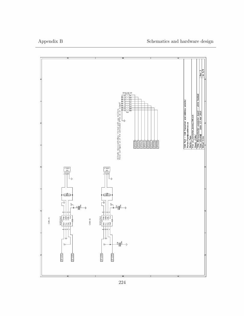
Appendix B
Schematics and hardware design
224

Appendix B
Schematics and hardware design
225

Appendix B
Schematics and hardware design
226

Appendix B
Schematics and hardware design
227

Appendix B
Schematics and hardware design
228

Appendix B
Schematics and hardware design
229

Appendix B
Schematics and hardware design
230

Appendix B
Schematics and hardware design
231
B.5 Filter inductor design
In order to design a filter inductor, requirements and assumption have to be known. For
the 1mH inductor design, these are:
Maximum expected peak current at 60Hz: 22A (15.5Arms = 110% rated cur-
rent)
Current ripples at switching frequency (20.4 kHz): 2A (peak-peak)
This design is based on a toroid inductor design guide29. According to this guide, the
no-load number of turns can be determined to be
ᵃ��� = �ᵃ�[ᵅ�ᵃ�]ᵃ��
=⎷
���10�ᵅ�ᵃ�
88ᵅ�ᵃ�ᵃ� �
= 107 ᵅ�ᵅ�ᵅ�ᵅ�ᵅ� (B.1)
The selected30 iron powder ring core has an ᵃ�� value of 88���� , a relative permeability
of 26ᵰ�, a path length of 18.4cm for the core circle and a volume of 91.4 cm3.
The maximum DC bias is expected to be
ᵃ�� = 107 ᵅ�ᵅ�ᵅ�ᵅ�ᵅ� × 22ᵃ�18.4ᵃ�ᵅ�
127.9 ᵃ�ᵃ�ᵃ�ᵅ�
(B.2)
From manufacturer data of XFLUX cores it can be determined that the permeability
shift due to core saturation effects will be at 85% of the nominal value. Hence, the
number of turns must be increased to keep the inductance high at high DC bias. A linear
interpolation offers a good approximation:
29 http://www.mag-inc.com/design/design-guides/inductor-design-with-magnetics-powder-cores 30 Mag-inc XFLUX 0078735A7

Appendix B
Schematics and hardware design
232
ᵃ��� = ᵃ���ᵅ�ℎᵅ�ᵃ�ᵅ�
= 107 ᵅ�ᵅ�ᵅ�ᵅ�ᵅ�85%
= 126 ᵅ�ᵅ�ᵅ�ᵅ�ᵅ�
The resulting new maximum DC bias will be
ᵃ�� = 126 ᵅ�ᵅ�ᵅ�ᵅ�ᵅ� × 22ᵃ�18.4ᵃ�ᵅ�
= 150.65ᵃ�ᵃ�ᵃ�ᵅ�
(B.3)
The resulting permeability shift decreases to 80%. Typically, the design is considered
sufficient after this iteration. Effects of stray inductances will have a more significant
influence on the resulting inductance than another few iterations.
The full load ᵃ�� value ᵃ��� becomes:
ᵃ��� = 88ᵅ�ᵃ�
ᵃ� � × 0.8 = 70.4���2
(B.4)
With 126 turns, the inductor is expected to have an inductance of 1.40mH at no load
and 1.12mH at no load. Reducing the number of turns to 113 turns yields an expected
inductance value of 0.90mH-1.12mH (during the implementation, the required cable
length has been determined to 48ft).
In order to calculate the expected inductor temperature, the core loss density (CLD)
for the material used must be known. In this case, ᵃ�ᵃ�ᵃ�[20ᵅ�ᵃ�ᵅ�] = ������� .
The resulting core losses due to high frequency switching are:
ᵃ�������� = 75 ᵅ�ᵃ�ᵃ�ᵅ�� × 91.4ᵃ�ᵅ�� = 6.92ᵃ� (B.5)
The losses in the copper wire at full load depend on its resistance:
ᵃ� = 0.00328 Ωᵅ�
× 113 ᵅ�ᵅ�ᵅ�ᵅ�ᵅ� × 0.129 ᵅ�ᵅ�ᵅ�ᵅ�ᵅ�
= 0.0478Ω (B.6)

Appendix B
Schematics and hardware design
233
Where 0.00328 �� is the resistance per meter of an AWG 11 wire. The resulting power
losses are:
ᵃ���������� = (15.5ᵃ�)� × 0.0478Ω = 11.5ᵃ� (B.7)
The total inductor losses at full load are expected to be:
ᵃ�������� + ᵃ���������� = 18.4ᵃ� (B.8)
Using an approximated equation, this results in an expected inductor temperature:
ᵃ���� = ᵃ���� + � ᵃ�ᵅ�ᵅ�ᵃ�ᵅ� ᵅ�ᵅ�ᵅ�ᵅ� (ᵅ�ᵃ�)
ᵅ�ᵅ�ᵅ�ᵃ�ᵃ�ᵃ�ᵃ� ᵃ�ᵅ�ᵃ�ᵃ� (ᵃ�ᵅ��)�
�����
= 25°ᵃ� + �18400ᵅ�ᵃ�271ᵃ�ᵅ�� � = 58.6°ᵃ�
(B.9)
All materials used are rated to at least 120°ᵃ� so that some room for even higher
overload currents is given.

Appendix C
Software
234
Software
C.1 Complex power limiting
This has been adapted from [72].
Code listing 1 Complex power limit transformation algorithm 1: Select channel priority (d/q) 2: If (priority is d) 3: Set d limit to complex limit 4: Compute d channel controller output ᵅ�ᵅ�ᵅ�� 5: Set q limit to �ᵅ�ᵅ�ᵅ�ᵅ�ᵅ��������
� − ᵅ�ᵅ�ᵅ���
6: Compute q channel controller output ᵅ�ᵅ�ᵅ�� 7: else 8: Set q limit to complex limit 9: Compute q channel controller output ᵅ�ᵅ�ᵅ�� 10: Set d limit to �ᵅ�ᵅ�ᵅ�ᵅ�ᵅ��������
� − ᵅ�ᵅ�ᵅ���
11: Compute d channel controller output ᵅ�ᵅ�ᵅ�� 12: end

Appendix C
Software
235
C.2 Additional software components – SMCU firm-
ware
AcBreakerController. Provides control over the AC breaker relay states, the
LED state indication and allows the ProtectionSystem to query the manual
override switch position.
CpuMonitor. Allows to read the current average load for CPU1, CPU2, CLA1
and CLA2.
AddressReader. Provides read access to an 8-bit DIP switch component with
which a CAN address for a simulation module and DC-bus voltage controller
module can be selected. Based on this address the correct sensor calibrations
for a specific module are loaded, as well.
DacGeneration. This is a debugging tool. Using the digital-to-analog outputs
A, B and C, digital values within the microcontroller can be visualized on an
oscilloscope in real-time. This is very useful if processes are to be monitored
that change with frequencies higher than 100 Hz.
DisplayController. This software block communicates with a 2x20 dot matrix
display via I2C bus to output selected messages. The first line always shows
current key sensor readings (simulation module: output active and reactive
power; DC-bus voltage controller module: DC-bus voltage). The second line
cycles a set of current pre-defined status messages that can be queued from any
program component.

Appendix C
Software
236
FanController. Forms the hardware proxy and hardware adapter for a maxi-
mum of two PWM controlled 12V DC fans. Its configuration is realized in the
FanControllerSettings.
InputButtonAdapter. This is a hardware adapter for three buttons on the Mi-
crocontroller adapter board to allow minimal manual control of the module
without communication link (e.g., emergency shutdown).
LEDIndicator. This component controls the status LED indications on the Mi-
crocontroller adapter board.
MeasDataSynchronizer. This class holds a copy of all measurements (MeasDataS-
torage) for use by all TaskScheduler tasks (update rate: 1 kHz). TaskScheduler
tasks must not access the original measurement data directly, because data
integrity is not guaranteed during the runtime of a TaskScheduler task. Instead,
the synchronized data must be used.
StartupSwitchesAdapter. Used only with the DC-bus voltage controller module.
It generates the command signals for the charge/discharge circuit IGBT gate
drivers.
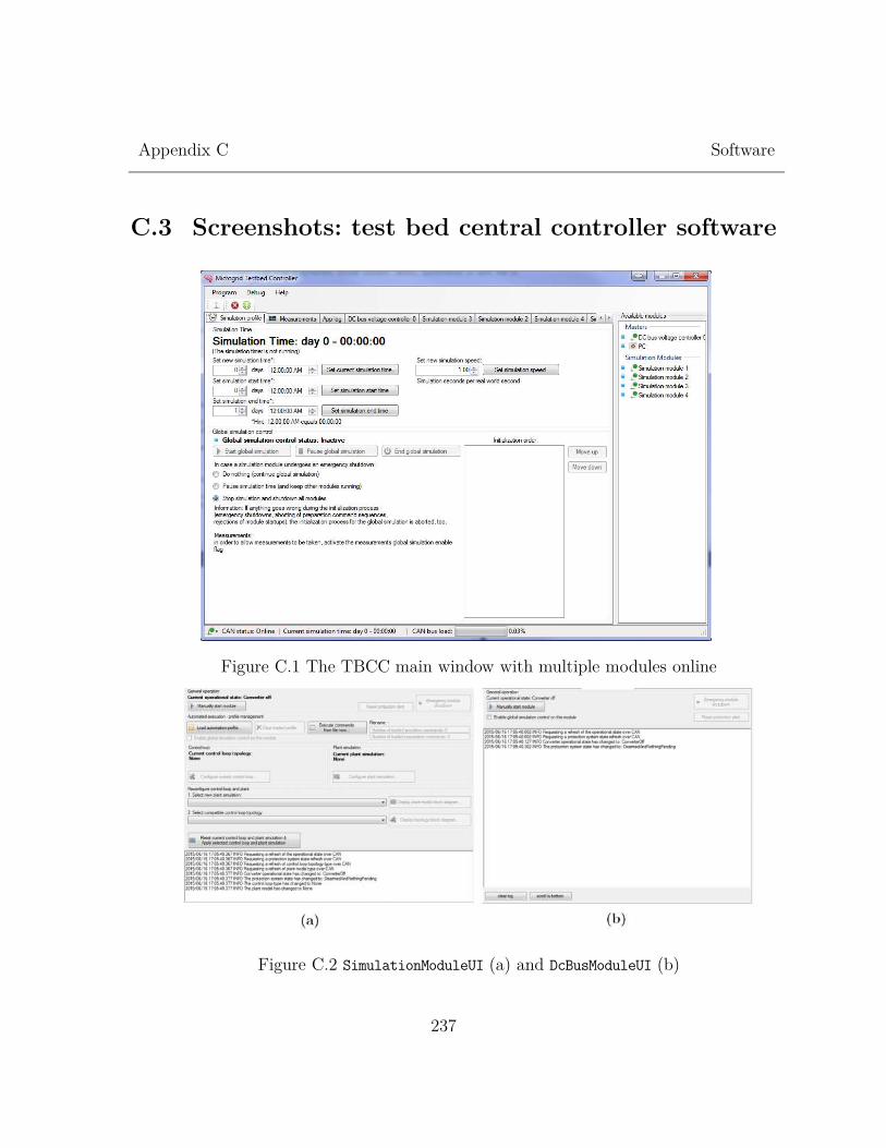
Appendix C
Software
237
C.3 Screenshots: test bed central controller software
Figure C.1 The TBCC main window with multiple modules online
Figure C.2 SimulationModuleUI (a) and DcBusModuleUI (b)

Appendix C
Software
238
Figure C.3 Example plot of a measurement of a PV plant variable
Figure C.4 Profile command display window with six commands loaded

Appendix C
Software
239
Figure C.5 Configuration dialog for the voltage-source based droop controller (a),
PV module parameter estimation after [63], [66] (b)

Appendix D
Bill of materials
240
Bill of materials
D.1 AC breaker box
Table D.1 BOM for one AC breaker unit
Manufacturer Manufacturer part number
Component refer-ences
Quan-tity
Unit Price [CAD]
TEXAS INSTRUMENTS SN74HC08N U3 1 0.67
AVX CORPORATION SR295E104MAR C1 C2 C3 C4 C5 C6
C8 C10 8 0.3 NICHICON (VA) UPJ1V151MPD6TD C7 C9 2 0.47
ON SHORE TECHNOLOGY INC ES1200/12DSFB 0 1 4.44 FCI DE09S064HTLF 0 1 1.76
EDAC INC 621-009-260-042 J1 1 2.38 TE CONNECTIVITY AMP 640455-2 P2 P3 P4 P5 4 0.13 TE CONNECTIVITY AMP 3-643813-2 0 4 0.21
SAMTEC INC TSW-150-07-T-S P1 0.1 2.74 0 0 P6 1 0 0 0 P7 P8 P9 P10 P11 5 0
NORCOMP INC 977-009-020R121 0 1 1.32 FAIRCHILD SEMICONDUC-
TOR 1N4148 D5 D6 D7 D8 4 0.13 FAIRCHILD SEMICONDUC-
TOR (VA) 1N4149TR D1 D2 D3 D4 4 0.13 BUD INDUSTRIES NBF-32018 0 1 31.92

Appendix D
Bill of materials
241
AMETHERM AS32 5R020 0 3 8.21 TOSHIBA SEMICONDUC-
TOR AND STORAGE TC74HC04APF U2 1 0.59 VISHAY SILICONIX IRF640PBF Q1 Q2 Q3 Q4 4 2
VISHAY SEMICONDUCTOR OPTO DIVISION ILQ615-4 U4 1 3.85
TE CONNECTIVITY AMP (VA) 2-520181-2 0 8 0.36
TE CONNECTIVITY AMP (VA) 4-520447-2 0 8 0.49
TE CONNECTIVITY POT-TER & BRUMFIELD T9AP1D52-12 0 4 5.56
STACKPOLE ELECTRON-ICS INC (VA) CF14JT10K0
R1 R2 R3 R4 R12 R13 6 0.13
STACKPOLE ELECTRON-ICS INC (VA) CF14JT13K0 R8 1 0.13
STACKPOLE ELECTRON-ICS INC (VA) CF14JT1K00 R15 R16 R23 R24 4 0.14
STACKPOLE ELECTRON-ICS INC (VA) CF14JT220R
R19 R20 R21 R22 R17 R18 R25 R26 8 0.14
STACKPOLE ELECTRON-ICS INC (VA) CF14JT330R R5 R6 R7 3 0.13
STACKPOLE ELECTRON-ICS INC (VA) CF14JT3K30 R9 R10 R11 R14 4 0.13
NXP 74HC595N U1 1 1.32 ON SHORE TECHNOLOGY
INC ED14DT 14PDIP 2 0.23 ON SHORE TECHNOLOGY
INC ED16DT 16PDIP 2 0.25 NKK SWITCHES M2112LCFW01 0 1 9.79 LITTELFUSE INC V20E140P 0 6 1.27
Total cost per unit, excluding PCB: CAD$ 122.36 (date: Q1/2015).
Total cost per unit, including PCB: CAD$ 132.36 (date: Q1/2015).

Appendix D
Bill of materials
242
D.2 Single-phase DC voltage sensor
For 0-550ᵃ���
Manufacturer
Manufacturer part
number
Component refer-
ences
Quan-
tity
Unit
Price
[CAD]
YAGEO (VA) MFP-25BRD52-15K R6 or R7 1 0.6
PHOENIX CON-TACT 1935161 0 5 0.37
LEM USA INC LV 20-P SENSV 1 42.35
KEMET C317C103K5R5TA C2 or C3 1 0.31
AVX CORPORA-TION SR295E104MAR C9 C10 C12 C13 5 0.3
MURATA ELEC-TRONICS NORTH
AMERICA RPER71H473K2K1A03
B C2 or C3 1 0.3
NICHICON (VA) UPJ1V151MPD6TD C5 C6 C7 C8 4 0.47
NXP SEMICON-DUCTORS (VA) BZX79-B3V0,133 ZA ZB ZC 3 0.22
KINGBRIGHT COMPANY LLC WP7113GD LEDN LEDP 2 0.15
YAGEO MFR-25FBF52-8K87 R6 or R7 1 0.13
YAGEO MFR-25FBF52-84R5 R 1 0.13
TE CONNECTIV-ITY AMP (VA) 5-1625890-8 RL 1 0.13

Appendix D
Bill of materials
243
STACKPOLE ELEC-TRONICS INC (VA) CF14JT620R RLEDP RLEDN 2 0.1
ON SHORE TECH-NOLOGY INC ED08DT 0 1 0.21
LINEAR TECHNOL-OGY LT1126CN8#PBF IC1A IC1B IC1C 1 8.37
VISHAY DALE (VA) RS01039K00FE73 Rin 1 3.1
Total cost per unit, excluding PCB: CAD$ 113.53 (date: Q1/2015).
D.3 Three-phase AC current sensor
For 35ᵃ�������
Manufacturer
Manufacturer
part number
Component refer-
ences Quantity
Unit
Price
[CAD]
YAGEO (VA) MFP-25BRD52-
100R
RSENS1A RSENS1B RSENS1C 3 0.46
PHOENIX CONTACT 1935161 5 0.37
YAGEO (VA) MFP-25BRD52-
3K3 R3A R3B R3C 3 0.46
LEM USA INC LA 55-P SENSI_A SENSI_B
SENSI_C 3 24.86
AVX CORPORATION SR295E104MAR C3 C4 C5 C6 C7 C8
C9 C10 8 0.3
NICHICON (VA) UPJ1V151MPD6T
D C1 C2 2 0.47

Appendix D
Bill of materials
244
NXP SEMICONDUC-TORS (VA) BZX79-B3V0,133 ZA ZB ZC 3 0.22
KINGBRIGHT COM-PANY LLC WP7113GD LEDN LEDP 2 0.15
TE CONNECTIVITY AMP (VA) 2-1676913-6 R4A R4B R4C 3 0.29
TE CONNECTIVITY AMP (VA) 1622796-6 R5A R5B R5C 3 0.42
STACKPOLE ELEC-TRONICS INC (VA) CF14JT620R RLEDP RLEDN 2 0.1
ON SHORE TECHNOL-OGY INC ED08DT 3 0.21
TEXAS INSTRUMENTS LM833N/NOPB IC1A IC1B IC1C 3 1.25
Total cost per unit, excluding PCB: CAD$ 119.85 (date: Q1/2015).
Total cost per unit, including PCB: CAD$ 124.85 (date: Q1/2015).
D.4 Three-phase AC voltage sensor
For 168ᵃ�������
Manufacturer
Manufacturer
part number
Component ref-
erences
Quan-
tity
Unit Price
[CAD]
YAGEO MFR-25FBF52-
113R
RSENS1A RSENDS1B RSENS1C 3 0.1
PHOENIX CONTACT 1935161 0 8 0.37

Appendix D
Bill of materials
245
LEM USA INC LV 20-P
SENSI_A SENSI_B SENSI_C 3 42.35
AVX CORPORATION SR295E104MAR C3 C4 C5 C6 C7
C8 C9 C10 8 0.3
NICHICON (VA) UPJ1V151MPD6TD C1 C2 2 0.47
NXP SEMICONDUC-TORS (VA) BZX79-B3V0,133 ZA ZB ZC 3 0.22
KINGBRIGHT COM-PANY LLC WP7113GD LEDN LEDP 2 0.15
TT ELECTRON-ICS/IRC (VA) GS-3-100-1502-F-LF
RSENS_A RSENS_B RSENS_C 3 0.96
TE CONNECTIVITY AMP (VA) 2-1676913-6 R4A R4B R4C 3 0.29
TE CONNECTIVITY AMP (VA) 1622796-6 R5A R5B R5C 3 0.42
STACKPOLE ELEC-TRONICS INC (VA) CF14JT620R RLEDP RLEDN 2 0.1
ON SHORE TECHNOL-OGY INC ED08DT 0 3 0.21
TEXAS INSTRU-MENTS LM833N/NOPB IC1A IC1B IC1C 3 1.25
Total cost per unit, excluding PCB: CAD$ 193.41 (date: Q1/2015).
Total cost per unit, including PCB: CAD$ 198.41 (date: Q1/2015).

Appendix D
Bill of materials
246
D.5 Microcontroller adapter board
Manufacturer
Manufacturer part
number
Component ref-
erences
Quan-
tity
Unit Price
[CAD]
YAGEO MFR-25FBF52-1K1 R11 1 0.13
YAGEO MFR-25FBF52-10R R91 1 0.13
YAGEO MFR-25FBF52-100R R7 R27 2 0.13
EVERLIGHT ELECTRONICS
CO LTD MV5374C D3 D8 2 0.6
EVERLIGHT ELECTRONICS
CO LTD MV5774C D4 1 0.6
YAGEO (VA) MFP-25BRD52-10K RS5_1 RS5_2
RS5_3 3 0.6
MARKTECH OP-TOELECTRONICS MT240-G-A D1 D2 D5 D6 D7 5 0.43
YAGEO MFR-25FBF52-113R R50 R61 R62 3 0.13
YAGEO (VA) MFP-25BRD52-1K RS4_1 RS4_2
RS4_3 3 0.6
FAIRCHILD SEMI-CONDUCTOR 1N4148 D11 D12 2 0.13
FAIRCHILD SEMI-CONDUCTOR
(VA) 1N4149TR D9 D10 2 0.13
FAIRCHILD SEMI-CONDUCTOR
(VA) 1N5226BTR D13 D14 D15 3 0.16

Appendix D
Bill of materials
247
TEXAS INSTRU-MENTS CD74AC244E U7 1 1.24
TEXAS INSTRU-MENTS TMDXDOCK28377D 0 1 297.03
TDK CORPORA-TION FK24X7R1H105K
C3 C4 C40 C41 C43 C44 6 0.52
BOURNS INC 4609X-101-391LF RR2 1 0.54
BOURNS INC 4609X-101-682LF RR3 1 0.54
AVX CORPORA-TION SR295E104MAR
C2 C5 C8 C9 C10 C11 C12 C13 C14 C15 C16 C17 C18 C19 C24 C25 C26 C27 C28 C29 C30 C31 C32 C33 C34 C35 C36 C37 C38
C39 C42 31 0.3
NICHICON (VA) UPJ1V151MPD6TD C6 C7 C22 C23 2 0.47
COPAL ELEC-TRONICS INC S-2150 SW4 1 4.88
EDAC INC 621-009-260-042 J1 1 2.38
YAGEO MFR-25FBF52-7K15 R15 R17 R67 R69 4 0.13
YAGEO MFR-25FBF52-715R R14 R16 R66 R68 4 0.13
TE CONNECTIV-ITY AMP 640456-6 CONNSPI1 1 0.39
TE CONNECTIV-ITY AMP 640454-2 P2 P3 P4 P5 4 0.17
TE CONNECTIV-ITY AMP 640455-2 P1 P11 P12 3 0.13

Appendix D
Bill of materials
248
TE CONNECTIV-ITY AMP 640455-3 K1 K2 K3 3 0.18
TE CONNECTIV-ITY AMP 640455-5 P6 1 0.26
TE CONNECTIV-ITY AMP 640455-6 CONN_SENS4 1 0.3
TE CONNECTIV-ITY AMP 640455-6 CONN_SENS3 1 0.3
TE CONNECTIV-ITY AMP 1-640455-0
CONN_PWM1 CONN_SENS1 CONN_SENS2 3 0.48
TE CONNECTIV-ITY AMP 4-644540-0 0 3 0.88
TE CONNECTIV-ITY AMP 3-640440-3 0 3 0.32
TE CONNECTIV-ITY AMP 3-640440-4 0 1 0.35
TE CONNECTIV-ITY AMP 3-643813-2 0 3 0.22
TE CONNECTIV-ITY AMP 3-643813-2 0 4 0.22
TE CONNECTIV-ITY AMP 3-644540-5 0 1 0.58
TE CONNECTIV-ITY AMP 3-644540-6 0 1 0.58
TE CONNECTIV-ITY AMP 5-1634503-1 P10 1 2.84

Appendix D
Bill of materials
249
FAIRCHILD SEMI-CONDUCTOR
(VA) BC548CTA Q3 1 0.28
STACKPOLE ELECTRONICS
INC (VA) CF14JT10K0 R87 R90 2 0.14
STACKPOLE ELECTRONICS
INC (VA) CF14JT120R R51 R52 R53 3 0.14
STACKPOLE ELECTRONICS
INC (VA) CF14JT1K00 R71 R75 2 0.14
STACKPOLE ELECTRONICS
INC (VA) CF14JT1K00 R2 R70 2 0.14
STACKPOLE ELECTRONICS
INC (VA) CF14JT20K0 R18 R20 2 0.14
STACKPOLE ELECTRONICS
INC (VA) CF14JT220R R72 R76 R77 R78 4 0.14
STACKPOLE ELECTRONICS
INC (VA) CF14JT2K20 R12 1 0.14
STACKPOLE ELECTRONICS
INC (VA) CF14JT2K70 R8 1 0.14
STACKPOLE ELECTRONICS
INC (VA) CF14JT3K30 R1 R73 R74 3 0.14

Appendix D
Bill of materials
250
STACKPOLE ELECTRONICS
INC (VA) CF14JT3K30
R34 R35 R36 R37 R38 R42 R43 R44 R45 R46 R47 R48
R49 13 0.14
STACKPOLE ELECTRONICS
INC (VA) CF14JT3K90 R21 R22 R23 R24
R25 R26 6 0.14
STACKPOLE ELECTRONICS
INC (VA) CF14JT750R
R28 R29 R30 R31 R32 R33 R54 R55 R56 R57 R58 R59
R60 13 0.14
STACKPOLE ELECTRONICS
INC (VA) CF14JT820R R13 R19 2 0.14
CTS ELECTRO-COMPONENTS 195-8MST RP1 1 1.51
ON SHORE TECHNOLOGY
INC 302-S101 CONNDISP1 1 0.36
ON SHORE TECHNOLOGY
INC ED08DT 0 1 0.21
ON SHORE TECHNOLOGY
INC ED08DT 0 2 0.21
ON SHORE TECHNOLOGY
INC ED14DT 0 4 0.23
ON SHORE TECHNOLOGY
INC ED14DT 0 1 0.23

Appendix D
Bill of materials
251
ON SHORE TECHNOLOGY
INC ED16DT 0 1 0.25
ON SHORE TECHNOLOGY
INC ED20DT 0 1 0.34
E-SWITCH KS-00Q-01 SW2 1 0.73
E-SWITCH KS-00Q-02 SW1 1 0.73
E-SWITCH KS-00Q-03 SW3 1 0.73
MEMORY PRO-TECTION DE-
VICES EP501B 0 1 1.11
VISHAY SEMI-CONDUCTOR
OPTO DIVISION ILD615-4 IC3 1 2.43
VISHAY SILI-CONIX IRF640PBF Q1 Q2 2 2.06
ON SEMICON-DUCTOR LM833NG U5 1 0.79
3M (VA) 3365/10 300SF 0 0.125 2.74
ON SEMICON-DUCTOR MC33079PG U6 1 1.86
MICROCHIP TECHNOLOGY MCP2562FD-E/P IC1 IC2 2 1.54
NEWHAVEN DIS-PLAY INTL
NHD-C0220BIZ-FSW-FBW-3V3M 0 1 13.47
OMRON ELEC-TRONICS INC-
EMC DIV XG4M-1030 0 1 1.23

Appendix D
Bill of materials
252
SAMTEC INC TSW-150-07-T-S various 3 2.82
TOSHIBA SEMI-CONDUCTOR
AND STORAGE TC74HC04APF U1 U2 U4 U8 4 0.61
OHMITE (VA) WHB2K5FET RS3_1 RS3_2
RS3_3 3 0.66812
Total cost per unit, excluding PCB: CAD$ 411.27 (date: Q1/2015).
Total cost per unit, including PCB: CAD$ 441.27 (date: Q1/2015).
D.6 Cost summary
Table D.2 Cost summary for Microgrid test bed housing expenses
Component Price in CAD
(approximated)
Server rack manipulation 700
Power plugs 60
Low-voltage power supplies 335
AC power terminal protection gear (breaker, fuses…), fix-
tures
141
USB-CAN adapter 333
Sum 1569

Appendix D
Bill of materials
253
Table D.3 Cost summary for DC-bus voltage controller module
Component Price in CAD
(approximated)
Heat sink (inventory) 0
IGBTs, power capacitors, power resistors 457
Microcontroller adapter board and microcontroller 440
2x2 gate drivers for discrete IGBTs 210
Fan 25
ᵪ�ᵃ� transformer 785
Sensors 415
Sum 2332
Table D.4 Cost summary for one simulation module
Component Price in CAD
(approximated)
Heat sink (donation) 0
IGBTs and related power components 340
Microcontroller adapter board and microcontroller 441
Sensors 561
LC Power filter components 56
ᵪ�ᵃ� transformer 785
Sum 2183

Bibliography
254
Bibliography
[1] B. Lasseter, “Microgrids [distributed power generation],” in IEEE Power Engineering Society Winter Meeting, 2001, 2001, vol. 1, pp. 146–149 vol.1.
[2] R. H. Lasseter, “Microgrids,” in Power Engineering Society Winter Meeting, 2002. IEEE, 2002, vol. 1, pp. 305–308.
[3] D. E. Olivares, A. Mehrizi-Sani, A. H. Etemadi, C. A. Canizares, R. Iravani, M. Kazerani, A. H. Hajimiragha, O. Gomis-Bellmunt, M. Saeedifard, R. Palma-Behnke, G. A. Jimenez-Estevez, and N. D. Hatziargyriou, “Trends in Microgrid Control,” IEEE Trans. Smart Grid, vol. 5, no. 4, pp. 1905–1919, Jul. 2014.
[4] J. M. Guerrero, J. C. Vasquez, J. Matas, L. G. de Vicuña, and M. Castilla, “Hierar-chical Control of Droop-Controlled AC and DC Microgrids: A General Approach Toward Standardization,” IEEE Trans. Ind. Electron., vol. 58, no. 1, pp. 158–172, 2011.
[5] E. de Jong, R. de Graaff, P. Vaessen, P. Crolla, A. Roscoe, F. Lehfu\s s, G. Lauss, P. Kotsampopoulos, and F. Gafaro, “European white book on real-time power hard-ware-in-the-loop testing,” Eur. Distrib. Energy Resour. Lab. DERlab Rep. No, 2011.
[6] M. Steurer, F. Bogdan, W. Ren, M. Sloderbeck, and S. Woodruff, “Controller and Power Hardware-In-Loop Methods for Accelerating Renewable Energy Integration,” in IEEE Power Engineering Society General Meeting, 2007, 2007, pp. 1–4.
[7] J.-Y. Kim, J. H. Park, and H.-J. Lee, “Coordinated Control Strategy for Microgrid in Grid-Connected and Islanded Operation,” in IFAC World Congress, 2011.
[8] K. Nam, J. Ahn, H. Choi, S. Kim, J. Kim, C. Cho, and J. Jeon, “Establishment of a pilot plant for KERI microgrid system based on power IT development program in Korea,” in Transmission Distribution Conference Exposition: Asia and Pacific, 2009, 2009, pp. 1–6.
[9] S. N. Bhaskara and B. H. Chowdhury, “Microgrids - A review of modeling, control, protection, simulation and future potential,” in 2012 IEEE Power and Energy Soci-ety General Meeting, 2012, pp. 1–7.
[10] “Microgrid Testbed | Golisano Institute for Sustainability | RIT.” [Online]. Available: https://www.rit.edu/gis/facilities/testbeds/microgrid%20testbed.php. [Accessed: 09-May-2015].

Bibliography
255
[11] L. Valverde, F. Rosa, A. J. del Real, A. Arce, and C. Bordons, “Modeling, simulation and experimental set-up of a renewable hydrogen-based domestic microgrid,” Int. J. Hydrog. Energy, vol. 38, no. 27, pp. 11672–11684, Sep. 2013.
[12] X. Wu, X. Yin, Q. Wei, Y. Jia, and J. Wang, “Research on Microgrid and its Appli-cation in China,” Energy Power Eng., vol. 05, no. 04, pp. 171–176, 2013.
[13] Y.-Y. Hong, Y.-Z. Lai, M.-C. Hsiao, Y.-R. Chang, Y.-D. Lee, and H.-C. Huang, “Studies on operation modes for the first outdoor microgrid test bed in Taiwan,” in 2012 IEEE International Conference on Power System Technology (POWERCON), 2012, pp. 1–6.
[14] R. H. Lasseter, J. H. Eto, B. Schenkman, J. Stevens, H. Vollkommer, D. Klapp, E. Linton, H. Hurtado, and J. Roy, “CERTS Microgrid Laboratory Test Bed,” IEEE Trans. Power Deliv., vol. 26, no. 1, pp. 325–332, 2011.
[15] J. Guerrero, “Intelligent Microgrid Project Research in Spain and Denmark,” pre-sented at the JEJU 2011 Symposium on Microgrids, Korea, May-2011.
[16] N. W. A. Lidula and A. D. Rajapakse, “Microgrids research: A review of experi-mental microgrids and test systems,” Renew. Sustain. Energy Rev., vol. 15, no. 1, pp. 186–202, Jan. 2011.
[17] C. N. A. T. 21 A. 2014, “Pulau Ubin micro-grid to be platform for energy-related technologies,” Eco-Business. [Online]. Available: http://www.eco-busi-ness.com/news/pulau-ubin-micro-grid-be-platform-energy-related-technologies/. [Accessed: 08-May-2015].
[18] M. Barnes, A. Dimeas, A. Engler, C. Fitzer, N. Hatziargyriou, C. Jones, S. Pa-pathanassiou, and M. Vandenbergh, “Microgrid laboratory facilities in Europe (UK, GER,...),” in 2005 International Conference on Future Power Systems, 2005, p. 6 pp.–6.
[19] E. Hossain, E. Kabalci, R. Bayindir, and R. Perez, “Microgrid testbeds around the world: State of art,” Energy Convers. Manag., vol. 86, pp. 132–153, Oct. 2014.
[20] “The Perfect Power Microgrid at IIT > ENGINEERING.com.” [Online]. Available: http://www.engineering.com/ElectronicsDesign/ElectronicsDesignArticles/Arti-cleID/6112/The-Perfect-Power-Microgrid-at-IIT.aspx. [Accessed: 09-May-2015].
[21] “CERTS Microgrid laboratory test bed - Pier final project report,” Lawrence Berke-ley National Laboratory, Feb. 2009.

Bibliography
256
[22] F. Huerta, J. K. Gruber, M. Prodanovic, and P. Matatagui, “A Power-HIL microgrid testbed: Smart energy integration lab (SEIL),” in 2014 IEEE Energy Conversion Congress and Exposition (ECCE), 2014, pp. 3998–4003.
[23] F. Huerta, J. K. Gruber, M. Prodanovic, P. Matatagui, and T. Gafurov, “A labora-tory environment for real-time testing of energy management scenarios: Smart En-ergy Integration Lab (SEIL),” in 2014 International Conference on Renewable En-ergy Research and Application (ICRERA), 2014, pp. 514–519.
[24] M. H. Rashid, Power electronics handbook devices, circuits, and applications. Bur-lington, MA: Butterworth-Heinemann, 2011.
[25] N. Mohan, T. M. Undeland, and W. P. Robbins, Power Electronics - Converters, Applications, and Design (3rd Edition). .
[26] J. Lettl, J. Bauer, and L. Linhart, “Comparison of Different Filter Types for Grid Connected Inverter.”
[27] P. A. Dahono, Y. R. Bahar, Y. Sato, and T. Kataoka, “Damping of transient oscil-lations on the output LC filter of PWM inverters by using a virtual resistor,” in , 2001 4th IEEE International Conference on Power Electronics and Drive Systems, 2001. Proceedings, 2001, vol. 1, pp. 403–407 vol.1.
[28] K. H. Ahmed, S. J. Finney, and B. W. Williams, “Passive Filter Design for Three-Phase Inverter Interfacing in Distributed Generation,” in Compatibility in Power Electronics, 2007. CPE ’07, 2007, pp. 1–9.
[29] J. Rocabert, A. Luna, F. Blaabjerg, and P. Rodríguez, “Control of Power Converters in AC Microgrids,” IEEE Trans. Power Electron., vol. 27, no. 11, pp. 4734–4749, Nov. 2012.
[30] K. . De Brabandere, B. Bolsens, J. . Van den Keybus, A. Woyte, J. Driesen, and R. Belmans, “A Voltage and Frequency Droop Control Method for Parallel Inverters,” IEEE Trans. Power Electron., vol. 22, no. 4, pp. 1107–1115, 2007.
[31] N. Pogaku, M. Prodanovic, and T. C. Green, “Modeling, Analysis and Testing of Autonomous Operation of an Inverter-Based Microgrid,” IEEE Trans. Power Elec-tron., vol. 22, no. 2, pp. 613–625, 2007.
[32] Y. A.-R. I. Mohamed and E. F. El-Saadany, “Adaptive Decentralized Droop Con-troller to Preserve Power Sharing Stability of Paralleled Inverters in Distributed

Bibliography
257
Generation Microgrids,” IEEE Trans. Power Electron., vol. 23, no. 6, pp. 2806–2816, Nov. 2008.
[33] E. Barklund, N. Pogaku, M. Prodanovic, C. Hernandez-Aramburo, and T. C. Green, “Energy Management in Autonomous Microgrid Using Stability-Constrained Droop Control of Inverters,” IEEE Trans. Power Electron., vol. 23, no. 5, pp. 2346–2352, 2008.
[34] S.-P. John, “Droop-Controlled Inverters Are Kuramoto Oscillators,” 2012, pp. 264–269.
[35] U. Borup, F. Blaabjerg, and P. N. Enjeti, “Sharing of nonlinear load in parallel-connected three-phase converters,” IEEE Trans. Ind. Appl., vol. 37, no. 6, pp. 1817–1823, Nov. 2001.
[36] R. H. Park, “Two-reaction theory of synchronous machines generalized method of analysis-part I,” Am. Inst. Electr. Eng. Trans. Of, vol. 48, no. 3, pp. 716–727, Jul. 1929.
[37] P. M. Anderson, A. A. Fouad, and Institute of Electrical and Electronics Engineers, Power system control and stability. Piscataway, N.J.: IEEE Press : Wiley-Inter-science, 2003.
[38] D. N. Zmood and D. G. Holmes, “Stationary frame current regulation of PWM inverters with zero steady-state error,” IEEE Trans. Power Electron., vol. 18, no. 3, pp. 814–822, 2003.
[39] R. Teodorescu, F. Blaabjerg, M. Liserre, and P. C. Loh, “Proportional-resonant con-trollers and filters for grid-connected voltage-source converters,” Electr. Power Appl. IEE Proc., vol. 153, no. 5, pp. 750–762, Sep. 2006.
[40] D. Sera, T. Kerekes, M. Lungeanu, P. Nakhost, R. Teodorescu, G. K. Andersen, and M. Liserre, “Low-cost digital implementation of proportional-resonant current con-trollers for PV inverter applications using delta operator,” in 31st Annual Conference of IEEE Industrial Electronics Society, 2005. IECON 2005, 2005, p. 6 pp.–.
[41] A. Luna, C. Citro, C. Gavriluta, J. Hermoso, I. Candela, and P. Rodriguez, “» Ad-vanced PLL structures for grid synchronization in distributed generation,«,” in u International Conference on Renewable Energies and Power Quality, Compostela, Španjolska, 2012.

Bibliography
258
[42] F. Blaabjerg, R. Teodorescu, M. Liserre, and A. V. Timbus, “Overview of Control and Grid Synchronization for Distributed Power Generation Systems,” IEEE Trans. Ind. Electron., vol. 53, no. 5, pp. 1398–1409, 2006.
[43] A. Timbus, M. Liserre, R. Teodorescu, and F. Blaabjerg, “Synchronization methods for three phase distributed power generation systems - An overview and evaluation,” in Power Electronics Specialists Conference, 2005. PESC ’05. IEEE 36th, 2005, pp. 2474–2481.
[44] S. M. Silva, B. M. Lopes, B. J. C. Filho, R. P. Campana, and W. C. Bosventura, “Performance evaluation of PLL algorithms for single-phase grid-connected sys-tems,” in Conference Record of the 2004 IEEE Industry Applications Conference, 2004. 39th IAS Annual Meeting, 2004, vol. 4, pp. 2259–2263 vol.4.
[45] J. C. Vasquez, J. M. Guerrero, M. Savaghebi, and R. Teodorescu, “Modeling, anal-ysis, and design of stationary reference frame droop controlled parallel three-phase voltage source inverters,” in 2011 IEEE 8th International Conference on Power Elec-tronics and ECCE Asia (ICPE ECCE), 2011, pp. 272–279.
[46] P. Hsu and M. Behnke, “A three-phase synchronous frame controller for unbalanced load [invertor operation],” in 29th Annual IEEE Power Electronics Specialists Con-ference, 1998. PESC 98 Record, 1998, vol. 2, pp. 1369–1374 vol.2.
[47] J. Liu, X. Qin, and Z. Yang, “Analysis of Zero-Sequence Circulating Current in Parallel PWM Inverter System with Difference of Carrier Wave Phases,” in Infor-matics in Control, Automation and Robotics, H. Tan, Ed. Springer Berlin Heidelberg, 2011, pp. 453–463.
[48] X. Wang, F. Zhuo, J. Li, L. Wang, and H. Huang, “Modeling and controlling of zero sequence current in directly paralleled 3-phase 4-wire inverter,” in Power Electronics Conference (IPEC), 2010 International, 2010, pp. 2377–2381.
[49] Z. Ye, “Modeling and Control of Parallel Three-Phase PWM Converters,” PhD The-sis, Virginia Polytechnic Institute and State University, Blacksburg, VA, USA, 2000.
[50] A. L. Julian, G. Oriti, and T. A. Lipo, “Elimination of common-mode voltage in three-phase sinusoidal power converters,” Power Electron. IEEE Trans. On, vol. 14, no. 5, pp. 982–989, 1999.

Bibliography
259
[51] M. M. Renge and H. M. Suryawanshi, “Three-Dimensional Space-Vector Modulation to Reduce Common-Mode Voltage for Multilevel Inverter,” IEEE Trans. Ind. Elec-tron., vol. 57, no. 7, pp. 2324–2331, Jul. 2010.
[52] A. K. Gupta and A. M. Khambadkone, “A Space Vector Modulation Scheme to Reduce Common Mode Voltage for Cascaded Multilevel Inverters,” IEEE Trans. Power Electron., vol. 22, no. 5, pp. 1672–1681, Sep. 2007.
[53] H. Zhang, A. von Jouanne, S. Dai, A. K. Wallace, and F. Wang, “Multilevel inverter modulation schemes to eliminate common-mode voltages,” IEEE Trans. Ind. Appl., vol. 36, no. 6, pp. 1645–1653, Nov. 2000.
[54] P. C. Loh, D. G. Holmes, Y. Fukuta, and T. A. Lipo, “Reduced common-mode modulation strategies for cascaded multilevel inverters,” IEEE Trans. Ind. Appl., vol. 39, no. 5, pp. 1386–1395, Sep. 2003.
[55] T. Logenthiran, “Multi-agent system for energy resource scheduling of integrated microgrids in a distributed system,” Electr. Power Syst. Res., vol. 81, no. 1, pp. 138–148, Jan. 2011.
[56] K. Zhuge, “Development of an Efficient Hybrid Energy Storage System (HESS) for Electric and Hybrid Electric Vehicles,” 2013.
[57] R. P. Sallen and E. L. Key, “A practical method of designing RC active filters,” IRE Trans. Circuit Theory, vol. 2, no. 1, pp. 74–85, Mar. 1955.
[58] H. W. Beaty, Ed., Handbook of electric power calculations, 3rd ed. New York: McGraw-Hill, 2001.
[59] J. C. Boemer, K. Burges, P. Zolotarev, J. Lehner, P. Wajant, M. Fürst, R. Brohm, and T. Kumm, “Overview of german grid issues and retrofit of photovoltaic power plants in germany for the prevention of frequency stability problems in abnormal system conditions of the ENTSO-E region continental europe,” in 1st International Workshop on Integration of Solar Power into Power Systems, 2011, vol. 24.
[60] M. Diaz-Aguilo, J. Sandraz, R. Macwan, F. De Leon, D. Czarkowski, C. Comack, and D. Wang, “Field-Validated Load Model for the Analysis of CVR in Distribution Secondary Networks: Energy Conservation,” IEEE Trans. Power Deliv., vol. 28, no. 4, pp. 2428–2436, Oct. 2013.
[61] A. Bokhari, A. Alkan, R. Dogan, M. Diaz-Aguilo, F. De Leon, D. Czarkowski, Z. Zabar, L. Birenbaum, A. Noel, and R. E. Uosef, “Experimental Determination of the

Bibliography
260
ZIP Coefficients for Modern Residential, Commercial, and Industrial Loads,” IEEE Trans. Power Deliv., vol. 29, no. 3, pp. 1372–1381, Jun. 2014.
[62] L. Hassaine, E. OLias, J. Quintero, and V. Salas, “Overview of power inverter topol-ogies and control structures for grid connected photovoltaic systems,” Renew. Sus-tain. Energy Rev., vol. 30, pp. 796–807, Feb. 2014.
[63] M. G. Villalva, J. R. Gazoli, and E. R. Filho, “Comprehensive Approach to Modeling and Simulation of Photovoltaic Arrays,” IEEE Trans. Power Electron., vol. 24, no. 5, pp. 1198–1208, 2009.
[64] J.-H. Jung and S. Ahmed, “Real-time simulation model development of single crys-talline photovoltaic panels using fast computation methods,” Sol. Energy, vol. 86, no. 6, pp. 1826–1837, Jun. 2012.
[65] G. Petrone, G. Spagnuolo, and M. Vitelli, “Analytical model of mismatched photo-voltaic fields by means of Lambert W-function,” Sol. Energy Mater. Sol. Cells, vol. 91, no. 18, pp. 1652–1657, Nov. 2007.
[66] M. G. Villalva, J. R. Gazoli, and E. R. Filho, “Modeling and circuit-based simulation of photovoltaic arrays,” in Power Electronics Conference, 2009. COBEP ’09. Brazil-ian, 2009, pp. 1244–1254.
[67] “Modeling and Simulation of Photovoltaic Arrays - Prof. Dr. Marcelo Gradella Vil-lalva.” [Online]. Available: https://sites.google.com/site/mvillalva/pvmodel. [Ac-cessed: 30-Jun-2015].
[68] A. N. A. Ali, M. H. Saied, M. Z. Mostafa, and T. M. Abdel-Moneim, “A survey of maximum PPT techniques of PV systems,” in 2012 IEEE Energytech, 2012, pp. 1–17.
[69] Natural Resources Canada, “Community Energy Planning - A Resource Guide for Remote Communities in Canada.” Natural Resources Canada, 17-May-2005.
[70] B. P. Douglass, Design patterns for embedded systems in C: an embedded software engineering toolkit, 1st ed. Oxford ; Burlington, MA: Newnes/Elsevier, 2011.
[71] Microsoft, “Model-View-Controller.” [Online]. Available: https://msdn.mi-crosoft.com/en-us/library/ff649643.aspx. [Accessed: 15-Jun-2015].
[72] Western Electricity Coordinating Council, Modeling and Validation Work Group, and Renewable Energy Modeling Task Force, “Generic Solar Photovoltaic System

Bibliography
261
Dynamic Simulation Model Specification,” Western Electricity Coordinating Coun-cil, Sep. 2012.