design of a v-band high-power sheet-beam coupled-cavity traveling-wave · pdf...
TRANSCRIPT

Progress In Electromagnetics Research, Vol. 123, 31–45, 2012
DESIGN OF A V-BAND HIGH-POWER SHEET-BEAMCOUPLED-CAVITY TRAVELING-WAVE TUBE
Y. Liu1, *, J. Xu1, Y. Wei1, X. Xu1, F. Shen1, M. Huang1,T. Tang1, W. Wang1, Y. Gong1, and J. Feng2
1National Key Laboratory of Science and Technology on VacuumElectronics, School of Physical Electronics, University of ElectronicScience and Technology of China, Chengdu 610054, China2National Key Laboratory of Science and Technology on VacuumElectronics, Beijing Vacuum Electronics Research Institute, Beijing100015, China
Abstract—The design and analysis of a high-power wideband sheet-beam coupled-cavity traveling-wave tube operating at V-band ispresented. The interaction circuit employs three-slot doubly periodicstaggered-ladder coupled-cavity slow-wave structure, and a 5 : 1 aspect-ratio sheet electron beam is used to interact with the circuit. Combinedwith design of the well-matched input and output couplers, a 3-Dparticle-in-cell model of the sheet-beam coupled-cavity traveling-wavetube is constructed. The electromagnetic characteristics and the beam-wave interaction of the tube are investigated. From our calculations,this tube can produce saturated output power over 630Watts rangingfrom 58 GHz to 64GHz when the cathode voltage and beam currentare set to 13.2 kV and 300mA, respectively. The correspondingsaturated gain and electron efficiency can reach over 32.5 dB and15.9%. Compared with the circular beam devices, the designed sheet-beam TWT has absolute advantage in power capability, and also it ismore competitive in bandwidth and electron efficiency.
1. INTRODUCTION
The V-band frequency range is a region of the millimeter-wave spectrum that has been developed mainly for inter-satellitecommunications [1]. As the key device, the amplifier criticallydetermines the performance of the whole inter-satellite systems. Due
Received 29 September 2011, Accepted 4 December 2011, Scheduled 12 December 2011* Corresponding author: Yang Liu ([email protected]).

32 Liu et al.
to its outstanding combined performances in power capacity andbandwidth, traveling-wave tube (TWT) is one of the most importantmillimeter-wave amplifiers [2–9]. As a full-metal structure, coupled-cavity has been shown to have excellent performance in powercapability. Consequently, there is considerable interest in the study anddevelopment of V-band coupled-cavity TWT. For example, Hughes-type coupled-cavity has been used to develop a 75Watts, 59–64 GHzTWT [10]. With computer simulation, we also designed a 100 Watts,58–62GHz TWT by using the double-staggered ladder coupled-cavitystructure [11]. However, both of them adopt the circular beam tunnel,the beam current will be restricted, and the maximum achievable powerwill be reduced as the beam tunnel size scale down.
In order to obtain higher power, the sheet electron beamhas been considered for beam-wave interaction in coupled-cavityTWT. A novel coupled-cavity structure for high-power widebandmillimeter-wave TWT, called sheet-beam coupled-cavity, is proposedby Simon J. Cooke etc. [12], as shown in Figure 1. The eigenmodecalculations and linear small-signal analyses by Larsen et al. [13] showthat this structure circuit has a significant gain and wide bandwidthwhen operating in Ka-band. Meanwhile, with the advent of moderncomputation, computer aided simulation has played an important rolein the design and development of the TWT, which can significantlyreduce the time and cost. Then, more and more engineers tend toperform simulation design before experimental study of the TWT [14–16]. In this paper, we will try to employ this novel structure to designa V-band TWT by means of computer simulation.
(a) (b)
Figure 1. (a) Cutaway view of the three-slot doubly periodicstaggered-ladder sheet-beam coupled-cavity solid model (with sheet-beam inserted in the beam channel). (b) The corresponding vacuummodel in our simulation (the background material is metal).
Progress In Electromagnetics Research, Vol. 123, 2012 33
The analysis and design of a V-band sheet-beam coupled-cavityTWT using Ansoft HFSS and CST studio suite [17–19] are presentedhere. In Section 2, the simulation model of the sheet-beam coupled-cavity structure is described in detail. High frequency propertiessuch as dispersion characteristics, beam-wave interaction impedanceare studied and optimized by HFSS. In Section 3, the input andoutput couplers are designed and the transmission characteristics ofthis circuit are obtained. In Section 4, a 3-D particle-in-cell modelof the V-band sheet-beam coupled-cavity TWT is constructed. Andthe beam-wave interaction simulations are performed to predict theoperating characteristics such as saturated output power, gain andelectron efficiency. Section 5 concludes with a summary and descriptionof future work.
2. SLOW-WAVE STRUCTURE DESIGN
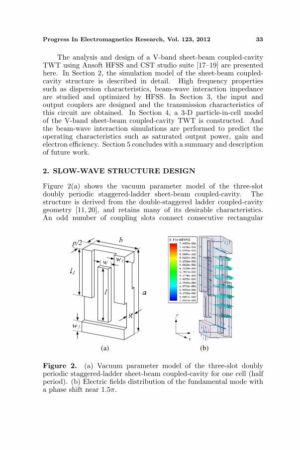
Figure 2(a) shows the vacuum parameter model of the three-slotdoubly periodic staggered-ladder sheet-beam coupled-cavity. Thestructure is derived from the double-staggered ladder coupled-cavitygeometry [11, 20], and retains many of its desirable characteristics.An odd number of coupling slots connect consecutive rectangular
(a) (b)
Figure 2. (a) Vacuum parameter model of the three-slot doublyperiodic staggered-ladder sheet-beam coupled-cavity for one cell (halfperiod). (b) Electric fields distribution of the fundamental mode witha phase shift near 1.5π.
34 Liu et al.
cavities in the waveguide structure. The slots are distributed evenlyaround the periphery, including one slot along a side wall, and thepattern is alternated so that consecutive sets of slots are offset, asin the traditional double-staggered ladder structure [20]. For theremainder of this paper, the z-axis is in the direction of electron beampropagation (the axial direction), the y-axis is in the wide dimensionof the structure, and the x-axis is in the short one.
Figure 2(b) plots the electric fields distribution of the fundamentalmode (mode 1 in Figure 3(a)) for the sheet-beam coupled-cavity witha phase shift near 1.5π. The electric fields are mainly concentratedaround the beam channel and have a predominant symmetric axialfield distribution along the electron beam propagation direction, whichis essential to beam-wave interaction of the TWT.
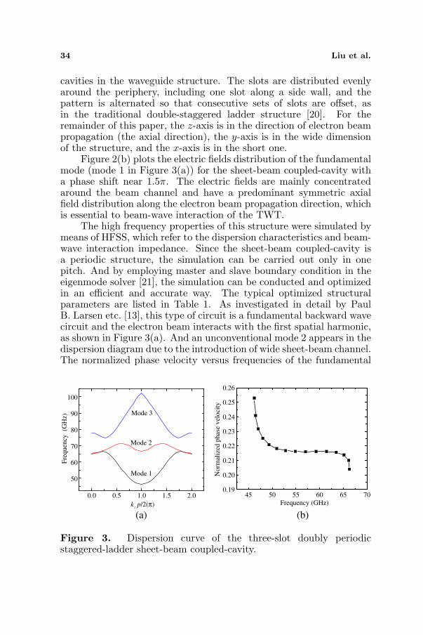
The high frequency properties of this structure were simulated bymeans of HFSS, which refer to the dispersion characteristics and beam-wave interaction impedance. Since the sheet-beam coupled-cavity isa periodic structure, the simulation can be carried out only in onepitch. And by employing master and slave boundary condition in theeigenmode solver [21], the simulation can be conducted and optimizedin an efficient and accurate way. The typical optimized structuralparameters are listed in Table 1. As investigated in detail by PaulB. Larsen etc. [13], this type of circuit is a fundamental backward wavecircuit and the electron beam interacts with the first spatial harmonic,as shown in Figure 3(a). And an unconventional mode 2 appears in thedispersion diagram due to the introduction of wide sheet-beam channel.The normalized phase velocity versus frequencies of the fundamental
0.0 0.5 1.0 1.5 2.0
50
60
70
80
90
100
Mode 3
Mode 2
Fre
qu
ency
(G
Hz)
Mode 1
45 50 55 60 65 700.19
0.20
0.21
0.22
0.23
0.24
0.25
0.26
No
rmal
ized
ph
ase
vel
oci
ty
Frequency (GHz)k p/2(π)z
(a) (b)
Figure 3. Dispersion curve of the three-slot doubly periodicstaggered-ladder sheet-beam coupled-cavity.

Progress In Electromagnetics Research, Vol. 123, 2012 35
Table 1. Parameters for the simulated SWS.
Parameter DimensionsCavity a× b 3.57× 1.98 mm
Cavity height (g) 0.41 mmSlot 1 & 2 width (w1) 0.46 mm
Slot 1 length (l1) 2.02 mmSlot 2 length 1.98 mm
Beam channel (l × w) 2.2× 0.44mmPeriod length (p) 1.64 mm
mode at the first spatial harmonic is also given in Figure 3(b). It showsthat the dispersion curve is quite flat over a broad bandwidth. Andthe phase velocity determines the beam voltage, approximately 13 kV,required for synchronized interaction with the electron beam.
As a measure of the interaction strength between the electronbeam and RF wave, the average interaction impedance over the cross-section of the electron beam (l/2×w/2) is also calculated by the fieldcalculator in the eigenmode solver of HFSS, as shown in the insert ofFigure 4. For calculating the average interaction impedance, we firstlyneed to divide the whole plane into small rectangular meshes. Then,it can be calculated by the following expression
Kaverage =
n∑1
snKn
S(1)
where, sn is the area of the nth mesh, Kn is the on-axis interactionimpedance [22] defined on the center position of the nth mesh, and Sis the whole area of the cross-section. If the area of each mesh is thesame, the expression can be simplified as
Kaverage =
n∑1
Kn
n(2)
The denser is the chosen mesh, the more accurate are thecalculation values. Here, we divide the plane into 400 (20 × 20)rectangular meshes. Then, by calculating the on-axis interactionimpedance of each mesh (Kn), the average interaction impedance overthe whole plane can be obtained by the formula (2), and the results areshown in Figure 4. Compared with the circular beam coupled-cavitystructure, the impedance values are basically at the same level [11].The sheet-beam can increase the beam power by distributing the beam

36 Liu et al.
0
5
10
15
20
25
30
35
45 50 55 60 65 70
Frequency (GHz)
Aver
age
imped
ance
(O
hm
s)Beam cross-section
y
xBeam channelcross-section
w/4 w/2
l/4
l/2
Figure 4. Average interaction impedance over the cross-section ofthe electron beam. (The right inset gives the cross-section view of theelectron beam.).
current over an increased area, which indicates that the sheet-beamcoupled-cavity TWT can obtain higher output power.
3. COUPLER DESIGN
A good coupler between the coupled-cavity circuit and theinput/output waveguide is important for improving tube efficiency,gain and stability over the required bandwidth. It also helps inpreventing the band-edge oscillation at the upper cut-off frequencyof the cavity mode [23]. Therefore, the design and optimization ofcoupler for coupled-cavity is a very important work. However, coupled-cavity is inherently three-dimensional structure and the design ofbroadband, low-VSWR coupler is a complicated process. The availableliteratures on this aspect are relatively sparse and mainly limited to thecircular beam structures [23, 24]. Furthermore, as sheet-beam coupled-cavity structures have more complex mode structure, designing a well-matched coupler would be more difficult.
Fortunately, a good design scheme for the sheet-beam coupled-cavity was proposed by Larsen et a. [25]. They designed an excellentcoupler for ka-band sheet-beam coupled-cavity structure, which wasalso verified by experiments. Therefore, we mainly design the couplerfor V-band sheet-beam coupled-cavity structure according to Larsen’sscheme. As shown in Figure 5(a), the coupler is a three-steppedrectangular waveguide placed into the short edge of the input cavity.The narrow side length of the lowest rectangular waveguide is equalto the cavity height (g). Then, there are mainly five free parameters

Progress In Electromagnetics Research, Vol. 123, 2012 37
(a) (b)
Figure 5. (a) Vacuum parameter model of the coupler. (b) Thetransmission vacuum model of the sheet-beam coupler-cavity circuit.
(c, g1, g2, h1 and h2) to be varied to optimize the VSWR within therange of interest. The transmission model of the sheet-beam coupler-cavity circuit including 25 periods of main section and input/outputcoupler is present, as shown in Figure 5(b). The boundary is set ascopper with the effective conductivity of 3.5 × 10⁷ S/m consideringsurface roughness [26, 27]. Using the transient solver in the CSTMicrowave Studio [18] and by sweeping the free parameters, theoptimal coupler for sheet-beam coupled-cavity structure is obtained.The optimized parameters for the coupler and the simulated thetransmission characteristics are given in Figure 6. The reflectionparameter S11 is almost below −20 dB in the frequency range of 58–64GHz. Together with the inset electric field distribution diagram, itdemonstrates that the designed coupler is well matched to the sheet-beam coupled-cavity circuit over a wide frequency range.
4. BEAM-WAVE INTERACTION SIMULATIONS
In this section, a 3-D particle-in-cell model of sheet-beam coupled-cavity TWT is constructed. The beam-wave interaction simulationsare carried out by using the PIC solver in CST Particle Studio [19] tosubstantiate the amplification capability of the TWT. As reflectionscaused by circuit discontinuities such as the mismatches between theinput/output couplers and the SWS can cause oscillation, severs shouldbe used to suppress these reflections [28]. Then, in order to obtain alarge gain and suppress the oscillation, the whole interaction circuit is

38 Liu et al.
-80
-70
-60
-50
-40
-30
-20
-10
0
S11
S21
Am
pli
tud
e (d
B)
y
z
c = 3.2 mmg = 0.95 mm
g = 1.55 mm
h = 0.85 mm
h = 1.25 mm
1
2
1
2
56 58 60 62 64 66
Frequency (GHz)
Figure 6. Transmission characteristics of the sheet-beam coupled-cavity circuit. (The lower left inset gives the z-component of electricfield distribution at 61 GHz in the longitudinal section).
Figure 7. 3-D particle-in-cell vacuum model of the sheet-beamcoupled-cavity TWT.
divided into two sections. The first section consists of 24 periods andthe other 30 periods, as shown in Figure 7. Here, output port 1 and2 are used as severs for suppressing the oscillation in our simulation.The dimensional parameters are listed in Table 1.
In the simulation, we assume that a sheet electron beam has across sectional area of 1.1 × 0.22mm2 (l/2 × w/2, as shown in theinset of Figure 4) in the central area of the beam channel with 13.2 kVvoltage and 300 mA current, corresponding to a beam aspect ratio of5 : 1 and beam filling factor of 25% with a current density of 124 A/cm2.And a uniform longitudinal magnetic field [29], with reasonable valueof 0.6 Tesla, is used here to confine the sheet electron beam. Theboundary is also specified as copper with the effective conductivity of3.5× 107 S/m.
The typical simulation results at the center frequency of 61GHzare exhibited in Figures 8–14. As can be seen from the power transfercurve in Figure 8, when the input power is small, the output powerincreases linearly with the input power, that is to say, the tube operates

Progress In Electromagnetics Research, Vol. 123, 2012 39
40
45
50
55
60
23 dBm
0 5 10 15 20 25Input power (dBm)
58.45 dBm
Ou
tpu
t p
ow
er (
dB
m)
Figure 8. Power transfer curveat 61 GHz.
-20 0 20 40 60 80 100Z (mm)
800
700
600
500
400
300
200
100
0
-100
Po
wer
(W
)
10 W
700 WOutput power atoutput port 3
Output power atoutput port 1
Figure 9. Growing wave plot asa function of the z-coordinate at61GHz.
-20-10
0102030405060708090
100110
Output
Input
Reflection
0 50 100 150 200Frequency (GHz)
Am
pli
tud
e (d
B(V
/m/G
Hz)
)
Figure 10. Frequency spectrumof input, output and reflectedsignals at 61GHz.
Beam channely
x
Figure 11. The cross-sectionview of the sheet electron beamat the end of the circuit.
in linear zone. But as the input power continues to grow, the tubewill operate in nonlinear zone. When the input power increases to200mW (23 dBm), the tube can be driven up to saturated statewith output power of 700Watts (58.45 dBm), which can also be seenfrom Figure 9. Figure 10 gives the frequency spectrum of input,output and reflected signal. As for the output signal, the spectrumis relatively pure. Although the higher harmonics are also aroused,the amplitudes are much lower than that of the operating frequency of61GHz. Meanwhile, it can be learnt that the reflected power is wellbelow the input power, which implies that the oscillation is unlikely tobe occurred.

40 Liu et al.
Figure 11 shows the cross-section view of the sheet electron beamat the end of the circuit. All of the electrons are well confined inthe beam channel, with no electron intercepted. Figure 12 gives theelectron bunching phenomenon around the end of the circuit. Theaccelerating electrons and retarding electrons are periodically arrangedalong the longitudinal direction, which demonstrates a good beam-wave energy exchange process. Figure 13 shows the phase momentumplot of the bunched electron beam along the longitudinal distance whenthe electron dynamic system has been in steady state. As the electronbeam propagates along the circuit, most of electrons experience acontinuous deceleration along the slow-wave circuit. This continuousinteraction results in a continuously increasing wave amplitude at theoutput port of the TWT, as depicted in Figure 14. The power atoutput port 1 is 10 Watts, corresponding to the gain of 17 dB for thesection one of the circuit. And the signal at output port 3 becomesstable at 700Watts, without oscillation.
Figure 12. The electron bunching phenomenon at 61 GHz.
Figure 13. Phase momentum (pz) plot of the bunched electron beamat 61 GHz.

Progress In Electromagnetics Research, Vol. 123, 2012 41
Figure 14. Input and output signals at 61 GHz.
58 59 60 61 62 63 64
Frequency (GHz)58 59 60 61 62 63 64
Frequency (GHz)
59.0
58.8
58.6
58.4
58.2
58.0
57.8
57.6Sat
ura
ted
ou
tpu
t p
ow
er (
dB
m) 28
26
24
22
20
18
Inp
ut
po
wer
(d
Bm
)
18.5
18.0
17.5
17.0
16.5
16.0
15.5
15.0
Ele
ctro
n e
ffic
ien
cy (
%)
(a) (b)
Figure 15. (a) The saturated output power versus input powerplots cross the bandwidth of 58–64GHz. (b) The saturated electronefficiency versus the frequency.
According to the same method, the TWT at each frequency canbe driven to the saturated state by adjusting the input power. Thesaturated output power versus input power plots across the bandwidthof 58–64 GHz is shown in Figure 15(a). The designed sheet-beamcoupled-cavity TWT can produce saturated output power of over630Watts (58 dBm) in the frequency range of 58–64 GHz, and thecorresponding saturated gain can reach over 32.5 dB. The maximumsaturated output power can reach 700 Watts at 61 GHz. Figure 15(b)gives the saturated electron efficiency versus the frequency, from whichwe can see that the saturated electron efficiency is greater than 15.9%across the bandwidth of 58–64 GHz.
Meanwhile, as the beam current density that we use here isrelatively low (124 A/cm2), the tube can obtain the higher output

42 Liu et al.
power by increasing the current density. And also, the electronefficiency can be further improved by means of phase velocitytapers [30], which will be an important research subject for the sheet-beam coupled-cavity TWT.
5. CONCLUSIONS
The three-slot doubly periodic staggered-ladder coupled-cavity withsheet electron beam is employed in V-band traveling-wave tube.It is believed that this is the first time that 3-D particle-in-cellsimulations have been conducted for a full-scale sheet-beam coupled-cavity traveling-wave tube. The simulation results show that thetube can produce a challenging output power over 630 Watts with abandwidth of 6 GHz, and the corresponding gain and electron efficiencycan reach over 32.5 dB and 15.9%. Compared with the circular beamdevices, the performance of our designed sheet-beam TWT is morecompetitive. Therefore, it is a promising slow-wave structure fordeveloping high-power, wideband and high efficiency millimeter-wavetraveling-wave tubes. Future work will be concentrated on the electronoptical system, especially on the formation, transmission and collectionof the sheet electron beam. Also, the experiment study of this sheet-beam coupled-cavity TWT will be carried out.
ACKNOWLEDGMENT
This work was financially supported in part by Vacuum ElectronicsNational Lab Foundation under Grant 9140C050101110C0501, andin part by the National Science Fund for Distinguished YoungScholars of China under Grant 61125103, and in part by theFundamental Research Funds for the Central Universities under GrantZYGX2009Z003 and ZYGX2010J054.
REFERENCES
1. Kornfeld, G. K., E. Bosch, W. Gerum, and G. Fleury, “60-GHzspace TWT to address future market,” IEEE Trans. ElectronDevices, Vol. 48, No. 1, Jan. 2001.
2. Kesari, V., “Beam-absent analysis of disc-loaded-coaxial waveg-uide for application in gyro-TWT (Part-1),” Progress In Electro-magnetics Research, Vol. 109, 211–227, 2010.

Progress In Electromagnetics Research, Vol. 123, 2012 43
3. Kesari, V., “Beam-present analysis of disc-loaded-coaxial waveg-uide for application in gyro-TWT (Part-2),” Progress In Electro-magnetics Research, Vol. 109, 229–243, 2010.
4. Kesari, V. and J. P. Keshari, “Analysis of a circularwaveguide loaded with dielectric and metal discs,” Progress InElectromagnetics Research, Vol. 111, 253–269, 2011.
5. Mustafa, F. and A. M. Hashim, “Properties of electromagneticfields and effective permittivity excited by drifting plasma wavesin semiconductor-insulator interface structure and equivalenttransmission line technique for multi-layered structure,” ProgressIn Electromagnetics Research, Vol. 104, 403–425, 2010.
6. Mineo, M., A. Di Carlo, and C. Paoloni, “Analytical designmethod for corrugated rectangular waveguide SWS THz vacuumtubes,” Journal of Electromagnetic Waves and Applications,Vol. 24, No. 17–18, 2479–2494, 2010.
7. Li, Z., J. H. Wang, F. Li, Z. Zhang, and M. Chen, “A new insightinto the radiation mechanism of fast and slow traveling waves,”Journal of Electromagnetic Waves and Applications, Vol. 25,No. 13, 1874–1885, 2011.
8. Shi, Z. J., Z. Q. Yang, F. Lan, G. Xi, F. Tao, and Z. Liang,“Investigation of a 30-GHz relativistic diffraction generator witha coaxial reflector,” Journal of Electromagnetic Waves andApplications, Vol. 24, No. 17–18, 2453–2462, 2010.
9. Malek, F., “The analytical design of a folded waveguide travelingwave tube and small signal gain analysis using Madey’s theorem,”Progress In Electromagnetics Research, Vol. 98, 137–162, 2009.
10. Wilson, J. D., P. Ramins, and D. A. Force, “A high-efficiency 59to 64 GHz TWT for intersatellite communications,” Proc. IEDMTech. Dig., 585–588, 1991.
11. Liu, Y., Y. B. Gong, Y. Y. Wei, J. Xu, Z. Y. Duan, andW. X. Wang, “Design of a 100-W V-band coupled-cavity,” China-Japan Joint Microwave Conference (CJMW), 458–460, Hangzhou,China, 2011.
12. Cooke, S. J., B. Levush, and T. M. Antonsen, Jr., “A coupled-cavity slow-wave structure for sheet-beam devices,” Proc. IEEEInt. Vac. Electron. Conf., 487–488, Monterey, CA, 2006.
13. Larsen, P. B., D. K. Abe, S. J. Cooke, B. Levush,T. M. Antonsen, Jr., and R. E. Myers, “Characterization of aKa-band sheet-beam coupled-cavity slow-wave structure,” IEEETrans. Plasma Sci., Vol. 38, No. 6, 1244–1254, Jun. 2010.

44 Liu et al.
14. Shin, Y. M., L. R. Barnett, and N. C. Luhmann, Jr., “Phase-shift traveling-wave-tube circuit for ultrawideband high-powersubmillimeter-wave generation,” IEEE Trans. Electron Devices,Vol. 56, No. 5, 706–712, May 2009.
15. Han, S. T., K. H. Jang, J. K. So, J. I. Kim, Y. M. Shin,N. M. Ryskin, S. S. Chang, and G. S. Park, “Low-voltageoperation of ka-band folded waveguide traveling-wave tube,” IEEETrans. Plasma Sci., Vol. 32, No. 1, 60–66, Feb. 2004.
16. Kim, H. J., H. J. Kim, and J. J. Choi, “MAGIC3D simulationsof a 500-W Ka-band coupled-cavity traveling-wave tube,” IEEETrans. Electron Devices, Vol. 56, No. 1, Jan. 2009.
17. Ansoft HFSS User’s Reference, Ansoft Corp. [Online] Available:http://www.ansoft.com.cn/.
18. CST MWS Tutorials, CST Corp. [Online] Available:http://www.cst-china.cn/.
19. CST PS Tutorials, CST Corp. [Online] Available:http://www.cst-china.cn/.
20. James, B. G. and P. Kolda, “A ladder circuit coupled-cavity TWTat 80–100 GHz,” Proc. IEDM Tech. Dig., Vol. 32, 494–497, 1986.
21. Booske, J. H., M. C. Converse, C. L. Kory, C. T. Chevalier,D. A. Gallagher, K. E. Kreischer, V. O. Heinen, andS. Bhattacharjee, “Accurate parametric modeling of foldedwaveguide circuits for millimeter wave traveling wave tubes,”IEEE Trans. Electron Devices, Vol. 52, No. 5, 685–693, May 2005.
22. Pierce, J. R., Traveling-wave Tubes, Van Nostrand, New York,1965.
23. Christie, V. L., M. Sumathy, L. Kumar, and S. Prasad,“Optimization of waveguide coupler for coupled-cavity TWTusing artificial neural network,” Proc. IEEE International VacuumElectronics Conference (IVEC), 263–264, 2010.
24. Kageyama, T., “The design of the transition region in coupled-cavity TWT,” Proc. IEEE International Vacuum ElectronicsConference (IVEC), 102–103, 2002.
25. Larsen, P. B., D. K. Abe, B. Levush, and T. M. Antosen, Jr.,“Coupling a waveguide input to a sheet-beam coupled-cavityslowe-wave structure,” Proc. IEEE International Vacuum Elec-tronics Conference (IVEC), 209–210, 2011.
26. Wilson, J. D. and C. L. Kory, “Simulation of cold-test parametersand RF output power for a coupled-cavity traveling-wave tube,”IEEE Trans. Electron Devices, Vol. 42, No. 11, Nov. 1995.

Progress In Electromagnetics Research, Vol. 123, 2012 45
27. Tischer, F. J., “Excess conduction losses at millimeter wave-lengths,” IEEE Trans. Microw. Theory Tech., Vol. 24, 853–858,Nov. 1976.
28. Gilmour, A. S., Jr., Principles of Traveling-Wave Tubes, ArtechHouse, Boston, MA, 1994.
29. Nguyen, K. T., J. A. Pasour, T. M. Antonsen, Jr., P. B. Larsen,J. J. Petillo, and B. Levush, “Intense sheet electron beamtransport in a uniform solenoidal magnetic field,” IEEE Trans.Electron Devices, Vol. 55, No. 5, 744–752, May 2009.
30. Wilson, J. D., “Design of high-efficiency wide-bandwidth coupled-cavity traveling-wave tube phase velocity tapers with simulatedannealing algorithms,” IEEE Trans. Electron Devices, Vol. 48,No. 1, Jan. 2001.