design of all-optical switches based on carrier injection in si/sio/sub 2/ split-ridge waveguides...
TRANSCRIPT
3454 JOURNAL OF LIGHTWAVE TECHNOLOGY, VOL. 24, NO. 9, SEPTEMBER 2006
Design of All-Optical Switches Based on CarrierInjection in Si/SiO2 Split-Ridge
Waveguides (SRWs)Fuwan Gan, Felix Jan Grawert, Jan-Malte Schley, Shoji Akiyama, Student Member, IEEE, Jürgen Michel,
Kazumi Wada, Lionel C. Kimerling, Member, IEEE, and Franz X. Kärtner, Senior Member, IEEE
Abstract—All-optical switches based on optical carrier injec-tion in high-index-contrast Si/SiO2 split-ridge-waveguide (SRW)couplers are analyzed. The waveguide devices are suitable for theconstruction of low-loss optical switch matrices as well as fast opti-cal switching. These devices exhibit robustness against fabricationtolerances, improved heat sinking, good carrier confinement, andhigh uniformity in transmission over the entire C-band of opti-cal communications, in contrast to comparable devices based onburied or ridge waveguides. Reasonably low electrical switchingpower of 1–10 mW is predicted for switching frequencies of 1 MHzto 1 GHz. Carrier recombination measurements in thin Si layerspassivated with different oxide layers confirm the feasibility of thedesigned switches and modulators.
Index Terms—All-optical switching, broadband coupler, carrierinjection, split-ridge waveguide (SRW).
I. INTRODUCTION
RAPIDLY increasing network traffic resulting from theworldwide increase in data communications demands
faster, cheaper, and more reliable switching and modulationdevices. In particular, attention has been drawn to optoelec-tronic integrated circuits (OEICs), which combine optical andelectronic functions on a single chip [1]–[5]. OEICs involveintegrated optics that provide large bandwidth, low loss, highspeed, and robustness against external electromagnetic inter-ferences (EMIs) paired with the advantages of large-scale mi-croelectronic circuits, namely the well-established technologyfor fabrication of densely integrated circuits. Future OEICs willcombine optical modulators, switches, detectors, emitters, andother optical components with electronic circuits and logic fortheir control.
Optical switches and modulators are the fundamental compo-nents of OEICs. Light is modulated in these devices by alteringthe reflectivity, transmission, or coupling between waveguidesby changing the refractive index and absorption in either thecore or cladding material of the waveguides. In the siliconplatform, the plasma effect [6], [7] and thermal effect [8] have
Manuscript received January 27, 2006; revised May 31, 2006. This work wassupported by NSF Grant ECS-0322740, DARPA Grant W911NF-04-1-0431,and the Microphotonics Center at the Massachusetts Institute of Technology.
The authors are with the Massachusetts Institute of Technology,Cambridge, MA 02139-4307 USA (e-mail: [email protected]; [email protected];[email protected]; [email protected]; [email protected]; [email protected]; [email protected]; [email protected]).
Color versions of Figs. 1–4 and 7 are available online at http://ieeexplore.ieee.org.
Digital Object Identifier 10.1109/JLT.2006.880157
been proven to be the most effective mechanisms for the im-plementation of optical switches. Silicon high-speed electroop-tic modulators with a small signal modulation bandwidth of1–10 GHz were demonstrated [9]–[11]. Most of the work fo-cused on electro/thermooptic switches [6], [8]; only a few stud-ies have been reported on all-optical switches [5]. In the latter,the flow of signal light is governed by control light at a differentwavelength [5], [12], [13]. In principle, all-optical switchescan work at much faster switching speeds than their electroniccounterparts due to the absence of bandwidth-limiting externalresistance–capacitance (RC) filters in the electrical connectionsat the expense of an optical pulse source. Additionally, all-optical structures generally do have less optical loss becauseconductive regions close to the optical mode, which usuallycause high optical loss, are not needed in this approach.
Silicon is the dominant material of the microelectronicsindustry. The availability of the well-established cost-effectivefabrication processes renders silicon an attractive choice foroptoelectronics for all applications where infrared light beyondthe silicon absorption edge is to be guided, filtered, modulated,and switched [5], [14]. In addition, optical components that canbe manufactured in a CMOS-compatible fabrication processpromise full integrability with CMOS microelectronic circuits.Thus, silicon offers a potential platform to integrate microelec-tronic and optical circuits.
So far, all-optical switches based on ring structures [5]have been demonstrated, which only operate over a limitedwavelength range around resonant frequencies. This motivatesthe search for a broadband modulator design. This work in-vestigates a Mach–Zehnder modulator that uses a split-ridgewaveguide (SRW) that merges the advantages of a buried anda ridge waveguide. The carriers are injected by a third pumpwaveguide carrying light that is efficiently absorbed in theparallel Si-SRW.
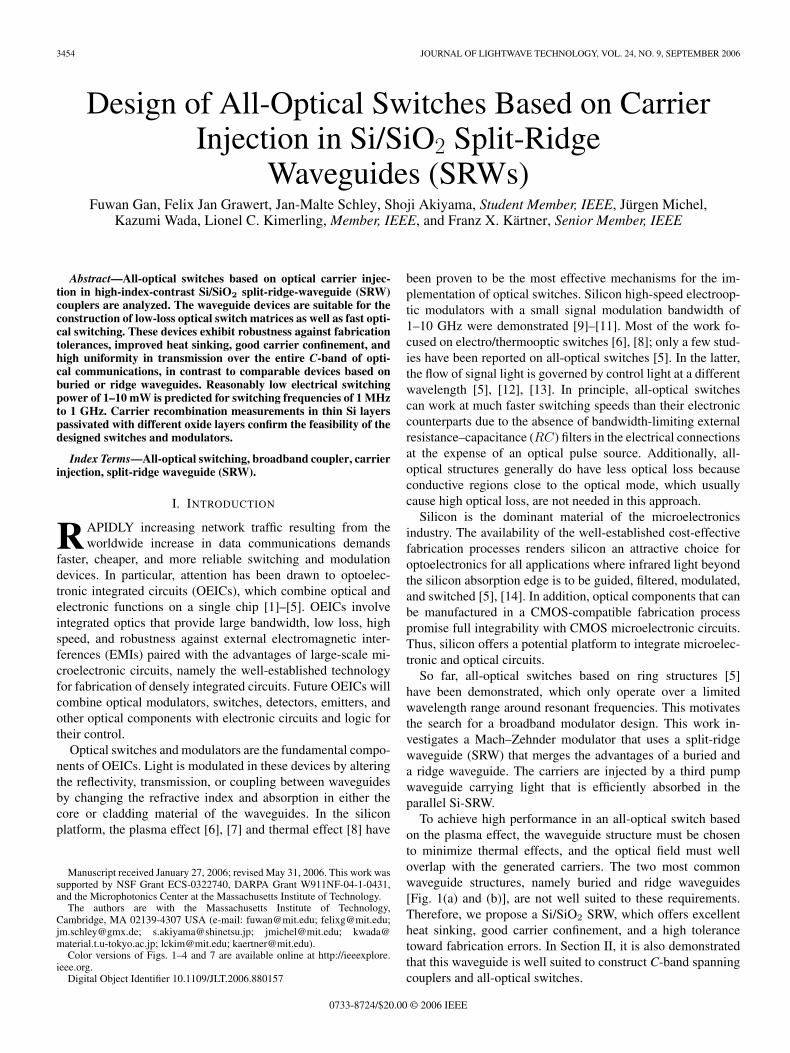
To achieve high performance in an all-optical switch basedon the plasma effect, the waveguide structure must be chosento minimize thermal effects, and the optical field must welloverlap with the generated carriers. The two most commonwaveguide structures, namely buried and ridge waveguides[Fig. 1(a) and (b)], are not well suited to these requirements.Therefore, we propose a Si/SiO2 SRW, which offers excellentheat sinking, good carrier confinement, and a high tolerancetoward fabrication errors. In Section II, it is also demonstratedthat this waveguide is well suited to construct C-band spanningcouplers and all-optical switches.
0733-8724/$20.00 © 2006 IEEE

GAN et al.: DESIGN OF ALL-OPTICAL SWITCHES BASED ON CARRIER INJECTION IN Si/SiO2 SRWs 3455
Fig. 1. Structure layout and single-mode profile for (a) buried waveguide,(b) ridge waveguide, (c) SRW.
In Section III, two architectures for all-optical carrier-injection switches using two or three waveguides are proposed.These switches exhibit large fabrication tolerances and lowpower consumption and show reduced undesired heating. Car-rier lifetime measurements in silicon bulk wafers as well assilicon-on-insulator (SOI) wafers passivated with different ox-ides show that the lifetimes assumed for the switch operationcan be achieved in real devices (Section IV).
The commercial simulator FIMMWAVE [15] was used todo mode solving, wave propagation, and coupling modeling.The program is based around a fully vectorial waveguidesolver based on the film mode matching method. It can findarbitrary order modes and mixed polarization, but it is not timedependent.
II. WAVEGUIDE AND COUPLER DESIGN FOR
ALL-OPTICAL SWITCHES
A. SRW
Waveguides are the most fundamental components of everyintegrated optical device. They ascertain confinement of lightand contain the active medium whose index is changed in thecase considered here and simultaneously act as a heat sink forthe energy deployed. High-index-contrast (HIC) waveguideswith a silicon core and SiO2 cladding offer the advantageof strong light and carrier confinement. Therefore, a shortinteraction length in optical switching applications using theplasma effect in silicon [7] is possible.
Two popular waveguide geometries on the Si/SiO2 platformare buried and ridge waveguides, as shown in Fig. 1(a) and (b).Typical dimensions of a single-mode buried waveguide in thismaterial platform are a width of 0.5 µm paired with a 0.2-µmheight [14]. For waveguides, the height can be rather wellcontrolled by chemical vapor deposition of the individual layersor with the SIMOX [16] or Smartcut process [17]. However,the lateral dimensions are determined by the accuracy of thephotolithography employed and can exhibit large deviationsfrom the design goal. The fabrication tolerances of the buriedsingle-mode waveguide are fairly small and easily deterioratethe performance in a fabricated device. The advantage of theburied waveguide is the tight optical confinement due to a smallmode size, which is often outweighed by strong device heatingcaused by the low thermal conductivity in the surroundingsilicon dioxide. In contrast, ridge waveguides exhibit muchlarger mode sizes and show a much larger fabrication toleranceof several micrometers [18], [19]. However, their open structureleads to low carrier confinement because the carriers can diffuseaway 62 µm within 100 ns in bulk silicon. Most carriers maydiffuse away upon carrier injection, which results in a lowcarrier concentration. Here, an Si/SiO2 SRW is investigatedto overcome these limitations and combine the advantages ofburied and ridge waveguide in a single structure.
An SRW can be considered a buried waveguide on top of aclosely spaced thin Si layer [see Fig. 1(c)]. The whole structureis embedded in SiO2. The thin layer draws part of the modedown from the buried waveguide. The amount of light guided inthe thin Si slab depends on the distance between the slab and theburied waveguide as well as the thickness of the slab. Hence, itsmode spreads out more in a buried waveguide but less in a ridgewaveguide, resulting in a lower center of the mode profile thanin the buried waveguide. Single-mode operation is obtainedby adjusting the vertical dimensions d1 and d2. Only the firsttransverse electric (TE) mode can be highly confined, the firsttransverse magnetic (TM) mode is confined very weakly, andno other modes can be guided. The Si slab makes the claddingeffective index somewhat larger than in the buried waveguideso that the index contrast is weaker than in a buried waveguide.Therefore, the SRW remains in the single mode for largerdimensions than a buried waveguide.
The SRW structure has a number of advantages over theburied and ridge waveguides. First, the insertion of the Si slaballows us to choose a larger width of the waveguide to reducesensitivity to fabrication errors while still maintaining single-mode operation by carefully adjusting the layer thickness. Forexample, at a communications wavelength of around 1.5 µm,a waveguide width of 1 µm, which is twice as large as for acomparable buried waveguide, can be chosen. In addition, thethickness of the isolating SiO2 layer is much smaller than inburied waveguides, resulting in a significant improvement inheat sinking. To achieve good heat sinking, the silicon slabthickness should be larger than 350 nm, and the heat sinkingis less than 5 µm away from the waveguide so that thermalresistance of silicon slab is smaller than the thin SiO2 layer.An electronic carrier-injection modulator design has made fulluse of this feature [20]. In our current proposed device, anSiO2 thickness d1 of less than 100 nm is sufficient, compared

3456 JOURNAL OF LIGHTWAVE TECHNOLOGY, VOL. 24, NO. 9, SEPTEMBER 2006
with 1–2 µm that would be required in a comparable buriedwaveguide, yielding a 10- to 20-fold improvement in thermalconductivity. Finally, the SRW allows for good confinement ofcarriers in the buried section, while they would easily escape inridge waveguides due to the open structure. Thus, the desiredswitching effect can be achieved at lower switching power.
B. Broadband Coupler With SRW
The aforementioned SRW also enables the design of couplersthat are less sensitive to fabrication variations and wavelength.This enables the construction of all-optical switches usingbroadband SRW couplers.
1) Fabrication Tolerances: Small length and thickness vari-ations are unavoidable in waveguide fabrication. We can dif-ferentiate between absolute width variations, i.e., errors thatresult in size changes for all devices on a wafer, and relativevariations, such as different thickness of adjacent waveguidesin an individual waveguide coupler. The coupling efficiency inwaveguide couplers tends to be particularly sensitive to relativeerrors of the adjacent waveguides. For example, the coupling ofa single-mode coupler at the communications wavelength basedon buried waveguides, with a cross-section of 400 × 200 nm, isfundamentally degraded by a deviation in feature size as smallas a few nanometers in the horizontal direction. The verticaldimension can be controlled much more precisely. Therefore,variations in vertical dimension are not considered. Even forstate-of-the-art E-beam fabrication techniques [21], the relativevariations in waveguide width can be controlled to be onlyon the order of 1 nm, which can cause a serious problem. Toobtain a worst-case estimate, we assume a relative variation of2.5 nm in the following calculations. A good design must besufficiently robust against fabrication errors.
In the following, the fabrication tolerance of the SRW cou-pler is investigated based on a simplified one-dimensional (1-D)model analytically and a three-dimensional (3-D) model nu-merically. With the first case, the SRW is modeled as a 1-Dslab waveguide. This approximation is chosen because theweak coupling in the devices studied is proportional to e−αL,which is dominated by the product of coupler length L and thefield decay coefficient (α) in the horizontal direction, whereasthe vertical field decay coefficient is of minor importance. Thecoupler length’s effect on tolerance is not going to be studiedin this paper; more information can be found in [22]. Thehorizontal cladding decay α of the symmetrical TM mode ina slab waveguide is governed by the following transcendentalequation [22]:
tan(kxω/2) =εcoεcl
α
kx(1)
where kx, ω, εco, and εcl are the horizontal wavenumber in thecore region, the core width, and the core and cladding dielec-tric constants, respectively. The relative change of field decayin the slab waveguide cladding ∆α/α0 = (∆α(w0 + ∆w) −∆α(w0))/α(w0) is calculated as a function of slab width inFig. 2. For waveguide widths below 0.5 µm, small variations inrelative thickness lead to a large relative change of field decay∆α/α0. In contrast, for a width of the waveguide exceeding
Fig. 2. Relative change of cladding decay coefficient ∆α/α0 as a functionof slab waveguide width with a waveguide width variation of 2.5 nm at thewavelength of λ = 1.55 µm.
1 µm, the relative change of field decay experiences merelya negligible drop. Thus, a coupler made out of waveguideswider than 1 µm will have considerably less change in cou-pling strength. Fig. 2 illustrates the significant improvement insensitivity against fabrication tolerances of SRW couplers dueto its larger waveguide width.
The insensitivity to fabrication errors has also been nu-merically verified in a 3-D coupler with single-mode SRWsat a communications wavelength of 1.55 µm by performingsimulations with the software FIMMWAVE [15]. For a 100%coupler with the waveguide dimensions w × h = 1 × 0.55 µm,layer thicknesses d1 = 100 nm and d2 = 350 nm [Fig. 1(c)],a 600-nm distance between the two quasi-TE single-modewaveguides, and 365-µm coupling length, our simulations showthat a relative fabrication error of 2.5 nm leads to a tolerabledrop in an output power of 0.11 dB. In contrast, in a quasi-TE single-mode coupler based on buried waveguides withthe dimensions of w × h = 450 × 250 nm, lateral distanced = 400 nm, and coupling length l = 180 µm, the same fab-rication error leads to an 8-dB power penalty. The computationwas done by keeping the waveguide center-to-center distanceconstant and varying the waveguide width only. These numbersillustrate the robustness of the SRW-based coupler with respectto fabrication tolerances.
The insensitivity to fabrication tolerances also leads towavelength insensitivity for a directional coupler because bothchanges in dimension and wavelength can substantially vary thewaveguide mode size and coupling strength. The wavelengthsensitivity of SRW couplers will be discussed in the followingsection.
2) Bandwidth: Another key requirement for all-opticalswitches is broadband behavior covering the entire C-band ofoptical communications with very low OFF-state insertion lossover the full bandwidth. For example, the construction of aswitch matrix with N = 64 channels may need a matrix of N2
couplers. In such a device, an individual channel encountersthe OFF state, i.e., the switch without carrier injection, up toa maximum of 2N − 2 times, whereas the ON state, i.e., theswitch with carrier injection, is encountered only once, whenthe signal is routed to a different channel. For our design,

GAN et al.: DESIGN OF ALL-OPTICAL SWITCHES BASED ON CARRIER INJECTION IN Si/SiO2 SRWs 3457
Fig. 3. Bandwidth for two-waveguide couplers based on buried (dashed) andSRW (solid) waveguides.
we found that the OFF state of each individual coupler is almostfrequency independent and does exhibit very low loss on theorder of only 1% (Fig. 3), neglecting additional waveguidelosses. Thus, the channel passing through the entire matrixof 64 switches would encounter an overall insertion loss ofonly 5.5 dB.
The broadband operation of the SRW coupler results fromthe large width of the waveguide, which induces less opticalconfinement and less wavelength sensitivity. The SRW couplerwith 1 µm width offers a significantly broader bandwidth thanthat based on the buried waveguide with a typical width of lessthan 0.5 µm. We verified this hypothesis also with the softwarepackage FIMMWAVE [15]. Our calculations reveal that theSRW coupler exhibits over 99% transmission over the entireC-band (Fig. 3), whereas the coupler based on buried wave-guides is a much narrower band, and its power transmissiondrops below 94% at both ends of the C-band. For a completeswitch matrix, such a high transmission uniformity of an SRWcoupler would be significant: With a seemingly small loss ofabout 1% in each buried waveguide coupler at 1530 nm, thetotal losses at this wavelength accumulate to maximally only5.5 dB in a 64-channel switch matrix, whereas the signal at thecenter wavelength of 1550 nm remains unattenuated. However,a 64-channel switch matrix based on buried waveguide couplerhas a maximum loss of 34 dB at a wavelength of 1530 nm.This problem is circumvented in the SRW coupler due to itslow variation in transmission over the entire C-band.
III. ALL-OPTICAL SWITCHES
In the last section, we demonstrated the advantage of usingSRWs to achieve a broadband coupler. In this section, we an-alyze two different architectures for all-optical switches basedon SWR couplers. The key attraction of all-optical switches isthe potential for high switching speeds and low insertion loss.The high speed results from the absence of RC lowpass filtersof the electrical drive circuitry, and the absence of significantoptical losses at the signal wavelength typically occurs inswitches due to the absorption of evanescent field componentsin the vicinity of the drive electrodes. All-optical switches havebeen realized at high power levels in large silicon structures
Fig. 4. Sketch of the proposed switches. (a) Two-waveguide switch.(b) Three-waveguide switch.
[23]. However, the high power regime and large dimensions ofthe silicon switches demonstrated to date render them inappro-priate for on-chip integration. Furthermore, recently, the pos-sibility of all-optical switching in the silicon material platformwas demonstrated by the injection of 500-ps pulses in a micror-ing resonator structure, resulting in an ultrafast switch [5]. Here,the design of all-optical ∆β switches is investigated. Switchingis triggered by carrier generation caused by absorbing 800-nmlight, which is coupled into the switch with a dedicated SiNwaveguide (Fig. 4). Our simulations (Sections III-B and C)and carrier lifetime measurements (Section IV) show that suchall-optical switches enable switching with continuous-wave(CW) control light at low optical power levels.
A. Switching Principle and Device Structures
The structures of the carrier-injection switches are depictedin Fig. 4. The switches are based on the SRW coupler discussedin Section II-A and a SiN injection waveguide for transportof the 800-nm modulation light. The modulation light is as-sumed to come from an off-chip source. Two different couplerarchitectures have been explored with two and three waveguideelements for the signal light, respectively (Fig. 4). The couplerconsisting of two waveguides [Fig. 4(a)] is suitable for highswitching speeds (exceeding 1 GHz) since carriers diffuse outof the active region along the signal waveguides. In contrast,the switch depicted in Fig. 4(b) comprises an additional middlesection in which the carriers are generated. The effective carrierlifetime in this structure is longer, since the surrounding isolat-ing material prevents the escape of the carriers, as discussedin Section II-A, such that switching can be maintained withvery low optical power if the surfaces are sufficiently well pas-sivated. The length of the active regions is chosen to allow forefficient coupling of the 800-nm control light from the injectionwaveguide. Numerical simulations show that, for a distancebetween control and signal waveguides of about 10–50 nm

3458 JOURNAL OF LIGHTWAVE TECHNOLOGY, VOL. 24, NO. 9, SEPTEMBER 2006
and for a length of the active zone of about 100 µm, over 90%of the control light is absorbed in the signal waveguide.
In the “OFF state” of the switch, no carriers are injectedinto the active region, and the input waveguide couples fullyto the output waveguide B–D. In this state, the system is ideallylossless, the switch is transparent, and the broadband transfercharacteristics from the input to output shown are in Fig. 3. Inthe case of the two-waveguide switch, coupling occurs directlyto the output waveguide B–D [Fig. 4(a)]; in case of the three-waveguide switch, coupling occurs via a short intermediatecoupling section into which the carriers are injected [Fig. 4(b)].In the “ON state” of the switch, control light entering the SiNwaveguide is absorbed in the active waveguide and changes theindex, which detunes the active waveguide. Now, coupling oflight to the output waveguide B–D is blocked, and almost alllight remains in the input waveguide A–C. The maximum lossin this state can be estimated by assuming that all the inputlight that is still coupled into the active region gets absorbedby the induced free carrier absorption. The next two sectionsdiscuss the performance for the two/three-waveguide switchesin detail.
B. Two-Waveguide All-Optical Switch
Here, we propose an all-optical switching structure capableof high-speed modulation. We start our analysis by investigat-ing the power transfer characteristics as a function of bulk car-rier lifetime, surface recombination, coupler dimensions, andother parameters. For this purpose, we calculate the switchingpower required to switch permanently from one channel to theother. Only the steady-state “ON” and “OFF” conditions areconsidered, and transients are neglected. Finally, we discussthe requirements for carrier lifetime to reach a certain switch-ing speed.
The power transfer characteristics of the device depend onthe changes in the refractive index and the absorption coeffi-cient between ON and OFF states as well as the recombinationtime constant τeff . Using the coupled mode theory, the poweroutput from port D in Fig. 4(a) can be written as [22]
PD = P0κ2
δ2 + κ2sin2(
√δ2 + κ2L) (2)
where L, κ, P0, and δ = (β1 − β2)/2 are the coupler length,the coupling coefficient, the input power into waveguide A,and the wavevector mismatch between the two waveguides,respectively. In the OFF state with δ = 0, the half beat lengthof the coupler is L = π/2κ to obtain full power transfer toport D. In the ON state δ = 0, the maximum power coupling toport D is
PDmax = P0κ2
δ2 + κ2(3)
and therefore, most optical power will remain in the input wave-guide if δ κ without considering absorption.
The transmission characteristics of the two-waveguideswitch in the ON and OFF states have been simulated usingFIMMWAVE. The separation between the two waveguides andthe coupling length are set to 0.6 and 365 µm, respectively.
Fig. 5. Two-waveguide switch performance. (a) Transmission to port D (inpercent). (b) Transmission to port C (in percent). (c) ON–OFF transmission ratio(in decibels).
The ON state is characterized by ∆nc = −0.005 and ∆α =26/cm caused by the carrier density change ∆ne/h = 1.8 ×1018 cm−3 [7]. The simulation results are shown in Fig. 5. Over98% of signal power is transmitted to port D in the OFF stateand more than 91.5% to port C in the ON state over the fullC-band, as shown in Fig. 5(a) and (b). The ON–OFF ratio foroutput port D is around 20 dB, which can be further increasedby increasing the pump power.
Now, we can estimate the required pump power consumptionnecessary to achieve such transmission characteristics. Thepump power can be calculated by
Pp =hc
λpηV gL (4)
where h, c, λp, η, and V are Planck’s constant, speed of light,pump wavelength, transfer efficiency, and active region volume.

GAN et al.: DESIGN OF ALL-OPTICAL SWITCHES BASED ON CARRIER INJECTION IN Si/SiO2 SRWs 3459
The generation rate is calculated by using (7) to be gL = 2 ×10¹⁷/ns · cm3, assuming ∆ne/h = 1.8 × 1018 cm−3 and τeff =10 ns. With λp = 800 nm and η = 95%, a pump power of10 mW is obtained for the given volume V of the active region.
An estimate for the thermal effects can be given based on thepump power used. The 100-nm SiO2 layer for the SRW dom-inates the thermal resistance Rtherm = dSiO2/(κSiO2 ·Aeff) +dSi.slab/(κSi ·Aeff.Slab) 250 K/W (assuming the heat sinkingis 1 µm away from the waveguide). The temperature risesby ∆T = Rtherm · Pp = 2.5 K, with a corresponding indexchange ∆nT = ∆T · 10−4/K = 2.5 × 10⁻⁴. Thus, the indexchanges caused by carrier injection are much larger thanthose due to thermal effects, and ∆nc/∆nT = 5 × 10⁻³/2.5 ×10−4 20 times in this case. Thus, heating effect can beneglected.
Altogether, these calculations show that the two-waveguideswitch has over 90% switching efficiency with a dc switchingpower as low as 10 mW. Carrier effects dominate thermaleffects by more than one order of magnitude, which allows forswitching speeds as fast as the carrier lifetime (Section III-D).The low heating of 2 K in the ON state (Section III-A) allows,for example, the construction of large switch matrices withswitching times approaching 10 ns.
C. Three-Waveguide All-Optical Switch
For many applications, especially switching matrices, muchslower switching times are often acceptable. To cover the slowoptical modulation bandwidth applications, the structure basedon three waveguides [see Fig. 4(b)] is advantageous.
Similar to the two-waveguide switching structure, the cou-pling strength κ and detuning δ determine the power transfercharacteristics. The working principle is shown in Fig. 4(b). Thethree waveguides are designed to have the same propagationconstant β0 without carrier injection. By injecting carriers intothe middle waveguide, the propagation constant in the middlewaveguide can be detuned by δ. According to the coupled modetheory [22], mode amplitudes in the output ports C and D[Fig. 4(b)] are given by
aC(z) = e−jβ0z ×[12−
(δ
8β′ −14
)e−j δ
2 z−jβ′z
+(
δ
8β′ +14
)e−j δ
2 z+jβ′z
](5)
aD(z) = e−jβ0z ×[−1
2−
(δ
8β′ −14
)e−j δ
2 z−jβ′z
+(
δ
8β′ +14
)e−j δ
2 z + jβ′z
](6)
where β′ = 1/2(δ2 + 8|κ|2)1/2. For the OFF state, substitutingaA(z = 0) = 1, |aD(z = L)| = 1, and δ = 0 into (5) and (6),we obtain the half beat length L = π/
√2|κ|. For maximum
power transfer to port C in the ON state, δ should be as largeas possible to keep most of the power in the input waveguide.
Simulations have been done for the three-waveguide couplerto obtain power transfer characteristics. The separation and
Fig. 6. Three-waveguide switch performance. (a) Transmission of port D (inpercent). (b) Transmission of port C (in percent). (c) ON–OFF transmission ratio(in decibels).
coupling length are set to 0.8 and 780 µm, respectively. Theactive region index change is set to 0.01, which is a little largerthan for two-waveguide coupler. Simulation results are shownin Fig. 6. In the OFF state, over 97% of the signal power istransmitted to port D and about 90% to port C in the ON stateover the C-band. The ON–OFF ratio of output port C is around30 dB, which is usually demanded for a switch [see Fig. 6(c)].
Performing the same calculations as for the two-waveguideswitch but using the carrier lifetime τ = 100 ns, the pumppower is estimated to be 2 mW, and the temperature rise is only∆T = 0.42 K. The induced index change is ∆nT = ∆T ×10−4/K = 4.2 × 10⁻⁵. The index change caused by the carrierinjection is, again, significantly larger than thermal effects,which is about ∆nc/∆nT = 10−2/4.2 × 10−5 230 times.Therefore, again, heating effects can be safely neglected.

3460 JOURNAL OF LIGHTWAVE TECHNOLOGY, VOL. 24, NO. 9, SEPTEMBER 2006
Comparing the modeling of two- and three-waveguideswitches, the two-waveguide switch may work well up to100 MHz, or even 1 GHz. The three-waveguide switch canoperate with slower switching speed because of its closedstructure helping to hold the carriers inside the active region.The 30-dB ON–OFF ratio of the three-waveguide switch withrespect to port C is large enough for optical communicationsapplications, and its power consumption and thermal effect areat leat as five times smaller than for the two-waveguide switch.
D. Switching Speed
As mentioned in the previous two sections, the switchingspeed is determined by the effective carrier recombination time.If carriers are injected to bring the switch to the ON state, ittakes several carrier lifetimes τeff for the switch to recoverto the unperturbed state. To design an all-optical switch withswitching speeds of up to 100 MHz, an effective recombinationtime of less than 1 ns is required. This value can be obtained byion-bombarding the active zone [24]. Under this condition, theeffective lifetime is shortened by Shockley–Read–Hall (SRH)recombination [20]. To obtain a switch with speeds of around1 MHz, an effective carrier lifetime of up to 100 ns is needed.Usually, for small thin waveguides, the surface recombinationdominates the recombination process. In order to fabricatethe designed switches, knowledge about the carrier lifetimefor thin Si waveguides with different surface passivation isnecessary.
IV. CARRIER LIFETIME MEASUREMENT
To verify the feasibility of the proposed two/three-waveguideswitches, the carrier lifetime was measured in bulk siliconwafers and SOI wafers, which are fabricated with the SmartCut Technique [17] and passivated with different oxide layers.The relaxation of a carrier density change in a silicon film isdetermined by four effects (i.e., SRH, radiative, Auger, andsurface recombination) [25] and is expressed as
d∆ne
dt= gL(t) −
[1
τSRH+
1τrad
+1
τAug+
1τsur
]∆ne (7)
where
1τrad
=B(2ni + ∆ne)
1τAug
= 3 × 10⁻²⁷(∆ne)1.8
and gL, τSRH, τrad, τsur, and B are the carrier generationrate, SRH, radiative, surface recombination lifetimes, andthe radiative recombination coefficient, respectively. RegularSRH recombination in pure crystalline silicon is on theorder of τSRH ≈ 10 ms [26] and can be neglected. Radiativerecombination in silicon is a minor process because of theindirect band gap [27], and Auger recombination plays onlya significant role at very high carrier density [28]. However,
for thin semiconductor layers, surface recombination is thedominant effect. The lifetime due to surface recombination ina thin layer is given by [25]
τsur =1
Damb
(d
π
)2
+d
2S(8)
where d is the film thickness, S is the surface recombination ve-locity, and Damb is the ambipolar carrier diffusion coefficient.The first item in (8) dominates for strong surface recombination(Sd/Damb 1) and the second term for weak surfacerecombination (Sd/Damb 1). The surface recombinationis determined by the surface recombination velocity S, whichstrongly depends on the surface passivation of the silicon film.
To determine the surface recombination velocity, the carrierlifetimes in both 650-µm-thick bulk crystalline silicon wafersand SOI wafers with a 1.5-µm low P-doped silicon layer(resistivity is around 1–30 Ω · cm) on top of a 3-µm SiO2 layermade by SIMOX [16] are studied. The carrier lifetimes for the650-µm-thick bulk silicon wafer and SOI layers are expectedto be on the order of 500 and less than 10 µs, respectively, atlow injection [25]. The surfaces of both kinds of samples arepassivated with two common types of oxide, namely 1) a naturalthermally grown silicon oxide and 2) an oxide layer made bylow-temperature oxidation (LTO). All oxide layers were 1000 Åthick. The natural oxide was thermally grown at 1000 Cunder atmospheric pressure, and the LTO layer was made ata temperature of 400 C and a pressure of 200 mtorr.
First, we extracted the surface recombination velocity fromthe passivated 650-µm-thick bulk silicon wafers by means ofradio-frequency photo-conductance delay spectroscopy (RF-PCD) [29] (see also [30]). Due to the thick bulk wafer, thecarrier lifetime falls in the range of 10–100 µs such that aslow measurement scheme like the RF-PCD is suitable forits characterization. The surface recombination velocity valuesfor the two different oxides were found to range from a low250 cm/s for the thermal oxide, which leads to a long carrierlifetime in the wafer of 137 µs, to a high surface recombinationvelocity of 1600 cm/s for the LTO (Table I), leading to aneffective carrier lifetime of only 35 µs. These values are ingood agreement with previously published data [25]. Based onthe values for the surface recombination velocity gained fromthe RF-PCD method, we expect overall carrier lifetimes τtotbetween 45 and 260 ns for the 1.5-µm-thick SOI films (seeTable I). Thus, a much faster measurement scheme is necessaryfor their characterization.
A dual-color measurement technique [31] as schematicallyillustrated in Fig. 7 was used to measure the carrier lifetimein the thin SOI layer. The method is capable of measuringlifetimes as short as 30 ns. The reflection from the surface ofthe wafer under test is measured with a low-power probe laserat 1550 nm, which is focused to a spot with a 120-µm radius onthe sample. A 532-nm laser with 80 mW of average power is fo-cused to the same spot size on the sample and brought to overlapwith the probe laser. The 532-nm light has an absorption lengthof 0.94 µm in the sample, such that about 80% of the incidentlight is absorbed in the 1.5-µm silicon film. The 532-nm beamis then modulated sinusoidally at frequencies ranging from

GAN et al.: DESIGN OF ALL-OPTICAL SWITCHES BASED ON CARRIER INJECTION IN Si/SiO2 SRWs 3461
TABLE IMEASUREMENT RESULTS
Fig. 7. Implementation of the dual-color carrier lifetime measurement.
30 kHz to 10 MHz with an acoustooptic modulator (AOM), re-sulting in a time-dependent carrier injection due to the absorp-tion in the sample. Due to the plasma effect (see Section III),the pump light causes a change in both the absorption and therefractive index of the thin silicon film. The reflection from thefilm is measured by lock-in detection. According to (7), forslow modulation of gL(t), the carrier density and the changesin the refractive index and absorption can follow the modulatedlight. However, for fast modulation, the carrier density cannotfollow the modulation. Thus, the corner frequency of the trans-fer characteristic describing index and absorption changes dueto pump light modulation is determined by the carrier lifetimein the sample. This lowpass effect is clearly observed in thecharacterization of the SOI wafer passivated with a thermaloxide (Fig. 8). From the corner frequency of the normalizedreflectivity change, a carrier lifetime of 150 ns is extracted.This value agrees within 50% with the value expected from themeasured value for the surface recombination velocity, whichconstitutes a rather good agreement, taking into account thatthe buried oxide of the SOI wafer is a thermal oxide but thatit is grown during the manufacturing process of the SOI waferunder unknown process conditions.
In contrast, the carrier lifetime of the SOI layers passivatedwith LTO could not be measured with the two-color pump-probe technique. As shown in Fig. 8, in these samples, thenormalized change in reflectivity lies about one order of mag-nitude below the reflectivity change for the sample with thethermal oxide. This fact indicates a carrier lifetime about oneorder of magnitude lower, since the magnitude of the changein reflectivity is proportional to the carrier lifetime at lowfrequencies. From the data at low frequencies, we can infer a
Fig. 8. Modulated reflectivity versus frequency for 1.5-µm-thick SOI waferspassivated by thermal and LTO oxides, respectively.
carrier lifetime at least ten times shorter than in the SOI waferpassivated with a thermal oxide, such that 15 ns can be assumedas an upper boundary for the carrier lifetime in these samples.
In a silicon single-mode waveguide, the layer thickness willbe even much thinner: on the order of 550 nm. For such athin layer, the carrier lifetime is shortened, at least by anotherfactor of 7. Thus, for a 550-nm-thin crystalline silicon layerwith a thermally grown silicon oxide cover layer, we estimatea carrier lifetime on the order of 50–100 ns. This short carrierlifetime enables the fabrication of the two-waveguide switcheswith modulation frequencies of 10 or 100 MHz, depending onwhich passivation layer is used. These measurements verify thefeasibility of the all-optical switches discussed in Section III.
V. CONCLUSION
In conclusion, we have designed an Si/SiO2 SRW that is tol-erant against fabrication errors and has excellent heat sinking.Based on this waveguide, we investigated broadband couplersand two- and three-waveguide all-optical switches. The cou-pler is wavelength-flatted over the C-band and is fabricationinsensitive. The designed switches show low loss, high ON–OFF
ratios up to 30 dB over the full C-band, and low pump-powerconsumption (around 1–10 mW). The switches enable, forexample, the construction of switching matrices with low powerconsumption and operating frequencies of 1 MHz to 1 GHz,depending on the surface passivation of the waveguides. Ofcourse, other means of carrier lifetime control can be employedsuch as ion bombardment.

3462 JOURNAL OF LIGHTWAVE TECHNOLOGY, VOL. 24, NO. 9, SEPTEMBER 2006
REFERENCES
[1] R. A. Soref, “Silicon-based optoelectronics,” Proc. IEEE, vol. 88, no. 12,pp. 1687–1706, Dec. 1993.
[2] G. Abstreiter, Engineering the future of electronics, vol. 5. London,U.K.: Physics World, Mar. 1992, pp. 36–39.
[3] L. C. Kimerling et al., “Monolithic silicon microphotonics,” in SiliconPhotonics, vol. 94, L. Pavesi and D. J. Lockwood, Eds. Berlin, Germany:Springer-Verlag, 2004, pp. 89–119.
[4] M. Salib, L. Liao, R. Jones, M. Morse, A. Liu, D. Samara-Rubio,D. Alduino, and M. Paniccia, “Silicon photonics,” Intel Technol. J., vol. 8,no. 2, May 10, 2004.
[5] V. R. Almeida, C. A. Barrios, R. R. Panepucci, and M. Lipson, “All-optical control of light on a silicon chip,” Nature, vol. 431, no. 7012,pp. 1081–1084, Oct. 28, 2004.
[6] P. Dainesi, L. Thevenaz, and P. Robert, “5 MHz 2 × 2 optical switch insilicon on insulator technology using plasma dispersion effect,” in Proc.27th ECOC, Amsterdam, The Netherlands, 2001, pp. 132–133.
[7] R. A. Soref and B. R. Bennett, “Electrooptical effects in silicon,” IEEE J.Quantum Electron., vol. QE-23, no. 1, pp. 123–129, Jan. 1987.
[8] M. W. Geis, S. J. Spector, R. C. Williamson, and T. M. Lyszczarz, “Sub-microsecond submilliwatt silicon-on-insulator thermooptic switch,” IEEEPhoton. Technol. Lett., vol. 16, no. 11, pp. 2514–2516, Nov. 2004.
[9] A. Liu, R. Jones, L. Liao, D. Samara-Rubio, D. Rubin, O. Cohen,R. Nicolaescu, and M. Paniccia, “High-speed silicon optical modula-tor based on a metal–oxide–semiconductor capacitor,” Nature, vol. 427,no. 6975, pp. 615–618, Feb. 2004.
[10] A. Liu, D. Samara-Rubio, L. Liao, and M. Paniccia, “Scaling the mod-ulation bandwidth and phase efficiency of a silicon optical modulator,”IEEE J. Sel. Topics Quantum Electron., vol. 11, no. 2, pp. 367–372,Mar./Apr. 2005.
[11] Q. Xu, B. Schmidt, S. Pradhan, and M. Lipson, “Micrometre-scale sil-icon electro-optic modulator,” Nature, vol. 435, no. 7040, pp. 325–327,May 19, 2005.
[12] M. Saito and T. Inoue, “Infrared optical switch by use of optically ex-cited free carriers in semiconductors,” Rev. Sci. Instrum., vol. 71, no. 5,pp. 2134–2135, May 2000.
[13] Y. Iida, Y. Omura, and H. Kobayashi, “Single-mode silicon optical switchwith T-Shape SiO2 waveguide as a control gate,” in Proc. IEEE Int. SOIConf., 2001, pp. 119–200.
[14] K. Kidoo Lee, “Transmission and routing of optical signals in on-chip waveguides for silicon microphotonics,” Ph.D. dissertation, Massa-chusetts Inst. Technol., Cambridge, MA, 2001.
[15] Photon Design, FIMMWAVE, 2002. Version 3.41.9.[16] R. A. Soref, E. Cortesi, F. Namavar, and L. Friedman, “Vertically in-
tegrated silicon-on-insulator waveguides,” IEEE Photon. Technol. Lett.,vol. 3, no. 1, pp. 22–24, Jan. 1991.
[17] M. Bruel, “Silicon on insulator material technology,” Electron. Lett.,vol. 31, no. 14, pp. 1201–1202, Jul. 6, 1995.
[18] R. A. Soref, J. Schmidtchen, and K. Pertermann, “Larger single-moderib waveguides in GeSi–Si and Si-on-SiO2,” IEEE J. Quantum Electron.,vol. 27, no. 8, pp. 1971–1974, Aug. 1991.
[19] J. Schmidtchen, A. Splett, B. Schuppert, and K. Pertermann, “Low losssinglemode optical waveguides with large cross-section in silicon-on-insulator,” Electron. Lett, vol. 27, no. 16, pp. 1486–1488, Aug. 1, 1991.
[20] F. Gan and F. X. Kärtner, “High-speed silicon electrooptic modulatordesign,” IEEE Photon. Technol. Lett., vol. 17, no. 5, pp. 1007–1009,May 2005.
[21] D. M. Tennanta, R. Fullowan, H. Takemura, M. Isobe, and Y. Nakagawa,“Evaluation of a 100 kV thermal field emission electron-beam nanolitho-graphy system,” J. Vac. Sci. Technol. B., vol. 18, no. 6, pp. 3089–3094,Nov./Dec. 2000.
[22] H. A. Haus, Waves and Felds in Optoelectronics. Englewood Cliffs, NJ:Prentice-Hall, 1984.
[23] A. Hache and M. Bourgeois, “Ultrafast all-optical switching in a silicon-based photonic crystal,” Appl. Phys. Lett., vol. 77, no. 25, pp. 4089–4091,Dec. 2000.
[24] F. E. Doany, D. Grischkowsky, and C.-C. Chi, “Carrier lifetime versusion-implantation dose in silicon on sapphire,” Appl. Phys. Lett., vol. 50,no. 8, pp. 460–482, Feb. 1987.
[25] R. Hull, Properties of Crystalline Silicon. London, U.K.:INSPEC, IEE, 1999.
[26] E. Yablonovitch and T. Gmitter, “Auger recombination in silicon atlow carrier densities,” Appl. Phys. Lett., vol. 49, no. 10, pp. 543–601,Sep. 1986.
[27] W. Gerlach, H. Schlangenotto, and H. Maeder, “On the radiative recom-bination rate in silicon,” Phys. Status Solidi A, vol. 13, p. 277, 1972.
[28] M. J. Kerr and A. Cuevas, “General parameterization of Auger recombi-
nation in crystalline silicon,” J. Appl. Phys., vol. 91, no. 4, pp. 2173–2480,Feb. 2002.
[29] G. L. Miller, D. A. H. Robinson, and J. D. Wiley, “Contactless mea-surement of semiconductor conductivity by radio frequency-free-carrierpower absorption,” Rev. Sci. Instrum., vol. 47, no. 7, pp. 799–805,Jul. 1976.
[30] G. L. Miller, “Method and apparatus for the contactless monitoring carrierlifetime in semiconductor materials,” US Patent 4 286 215, Aug. 25, 1981.
[31] P.-C. Yang and S. S. Li, “Measurements of film carrier lifetimes in silicon-on-insulator wafers by a contactless dual-beam optical modulation tech-nique,” Appl. Phys. Lett., vol. 61, no. 12, pp. 1408–1410, Sep. 1992.
Fuwan Gan received the B.S. and S.M. degrees inelectrical engineering from Shanghai Jiaotong Uni-versity, Shanghai, China, in 1997 and 2000, respec-tively. He is currently working toward the Ph.D.degrees in electrical engineering and computer sci-ence at the Massachusetts Institute of Technology,Cambridge.
His research interests include all-optical switch-ing, high-speed silicon electrooptic modulators, andintegrated photonic devices and systems.
Mr. Gan is a Student Member of the OpticalSociety of America and LEOS.
Felix Jan Grawert received the M.S. degree from the Georgia Institute ofTechnology, Atlanta, in 2000, the diploma degree from the University ofKarlsruhe, Karlsruhe, Germany, in 2001, and the Ph.D. degree from the Massa-chusetts Institute of Technology (MIT), Cambridge, in 2005, all in electricalengineering.
He was a scholar of the German National Academic Foundation, a Fulbrightscholar, and a Presidential Fellow at MIT. His research interests concentrate onlaser dynamics, mode-locked lasers, and integrated optics.
Dr. Grawert is a member of the Optical Society of America.
Jan-Malte Schley received the diploma degree from the University of Karl-sruhe, Karlsruhe, Germany, in 2002, and the Ph.D. degree from Universityof the Federal Armed Forces, Munich, Germany, in 2005, both in electricalengineering.
From 2003 to 2005, he worked for a large semiconductor company in thedevelopment of a novel Flash memory technology. Currently, he is aiming tobecome a patent attorney.
Dr. Schley is a member of the German Scholarship Foundation.
Shoji Akiyama (S’03) received the B.S. and M.S. degrees in chemistry fromKyoto University, Kyoto, Japan, in 1995 and 1997, respectively, and the Ph.D.degree from the Massachusetts Institute of Technology (MIT), Cambridge,in 2005.
In 1997, he joined Shin-Etsu Chemical Co., Ltd. In 2000, he joined Prof.L. C. Kimerling’s group at the Department of Materials Science and Engineer-ing, MIT. His research interest is microphotonics.

GAN et al.: DESIGN OF ALL-OPTICAL SWITCHES BASED ON CARRIER INJECTION IN Si/SiO2 SRWs 3463
Jürgen Michel received the diploma in physics from the University of Cologne,Cologne, Germany, in 1983 and the Ph.D. degree in applied physics from theUniversity of Paderborn, Paderborn, Germany, in 1987.
He was with the University of Paderborn as a Research Scientist. Priorto joining the Massachusetts Institute of Technology (MIT), Cambridge, in1990, he was with AT&T Bell Laboratories, Holmdel, NJ, as a PostdoctoralMember of the Technical Staff, studying defect reactions and defect propertiesin semiconductor materials. He is currently a Principal Research Associate atthe Microphotonics Center, MIT. He manages and conducts research projectson silicon-based photonic materials and devices and contamination issues insilicon processing. His main focus is currently on optical-clock distributionand coupling and packaging issues in microphotonics and on-chip wavelength-division-multiplexing (WDM) devices. He has authored and coauthored morethan 80 technical articles.
Kazumi Wada received the B.S., M.S., and Ph.D.degrees in instrumentation engineering from KeioUniversity, Yokohama, Japan, in 1973, 1975, and1982, respectively.
He is currently a Professor at the Department ofMaterials Engineering, University of Tokyo, Tokyo,Japan, conducting research of Si microphotonics.Prior to joining the University of Tokyo in 2004, hehas been with the Microphotonics Center, Depart-ment of Materials Science and Engineering, Massa-chusetts Institute of Technology (MIT) Cambridge,
conducting research on silicon-based photonic integrated circuits. Prior tojoining MIT in 1998, he was engaged in research on defects in silicon and III–Vsemiconductor materials and devices, including oxygen precipitation kinetics inSi with the NTT Research Laboratories. His current interest is on-chip opticalinterconnection for high-speed silicon-based large-scale integrations. He hasauthored and coauthored more than 100 refereed journal papers and has edited13 books.
Dr. Wada is a member of the Board of Directors of the Materials ResearchSociety.
Lionel C. Kimerling (M’89) received the S.B. degree in metallurgical en-gineering and the Ph.D. degree in materials science from the MassachusettsInstitute of Technology (MIT), Cambridge, in 1965 and 1969, respectively.
He was formerly the Head of the Materials Physics Research Department,AT&T Bell Laboratories, Holmdel, NJ. He is presently the Thomas LordProfessor of Materials Science and Engineering at MIT. In addition to histeaching duties in electronic, optical, and optoelectronic materials, he is theDirector of the Materials Processing Center, MIT. His current research ison silicon processing addresses, photovoltaic cells, environmentally benignintegrated circuit manufacturing, and monolithic microphotonic devices andcircuits.
Franz X. Kärtner (S’87–M’89–SM’02) was born in Cham, Germany, in 1961.He received the diploma and Ph.D. degrees in electrical engineering from theTechnical University, Munich, Germany, in 1986 and 1989, respectively.
From 1991 to 1993, he was with the Massachusetts Institute of Technology(MIT), Cambridge, as a Feodor–Lynen Research Fellow of the Alexander vonHumboldt Foundation. From 1993 to 1997, he was with the Swiss FederalInstitute of Technology (ETH), Zurich, Switzerland, as a Principal Investigator.After spending 1998 as a Visiting Assistant Professor at MIT, he joined theDepartment of Electrical Engineering, University of Karlsruhe (TH), Karlsruhe,Germany, where he held the Chair for Photonics and Terahertz Technologyand headed the High-Frequency and Quantum Electronics Laboratory. In 2001,he joined the Department of Electrical Engineering and Computer Science,MIT. His current research interests include ultrashort pulse generation, ultrafastphenomena, frequency metrology, and noise in microwave oscillators andoptical devices.
Dr. Kärtner is a member of the German Scholarship Foundation, the GermanPhysical Society, and the Optical Society of America.