design of bandpass delta-sigma modulators: avoiding...
TRANSCRIPT
Baker/Saxena 1
Design of Bandpass Delta-Sigma Modulators:
Avoiding Common Mistakes
R. Jacob Baker and Vishal Saxena
Department of Electrical and Computer Engineering
Boise State University
1910 University Dr., ET 201
Boise, ID 83725
Abstract –Implementation of analog-to-digital converters in the IF stage of a communication receiver can employ bandpass delta-sigma modulation (BPDSM). The benefit of using BPDSM is the ease with which in-phase (I) and quadrature (Q) components of the information can be extracted and translated to DC (to minimize both power and the required operating speeds). BPDSM topologies are commonly based on a cascade of resonators with transfer functions of z−2/(1 + z−2). This talk will show that these topologies, seen frequently in the literature, are always unstable. Discussions concerning the design of BPDSM-based analog-to-digital converters, in the IF stage, will be presented including why two or more paths are required and the details of implementing I/Q demodulation. Finally, examples will be given that show how the design topologies are applied.

Baker/Saxena 2
Low Pass Delta-Sigma Modulation (DSM)
� A low pass second order delta sigma modulator is described by the
following transfer function
� This equation is implemented using
}
( )48476NTF
STF
zzEzzXzY211 1)()()( −− −⋅+⋅=
11
1−− z
1
1
1 −
−
− z
z
Baker/Saxena 3
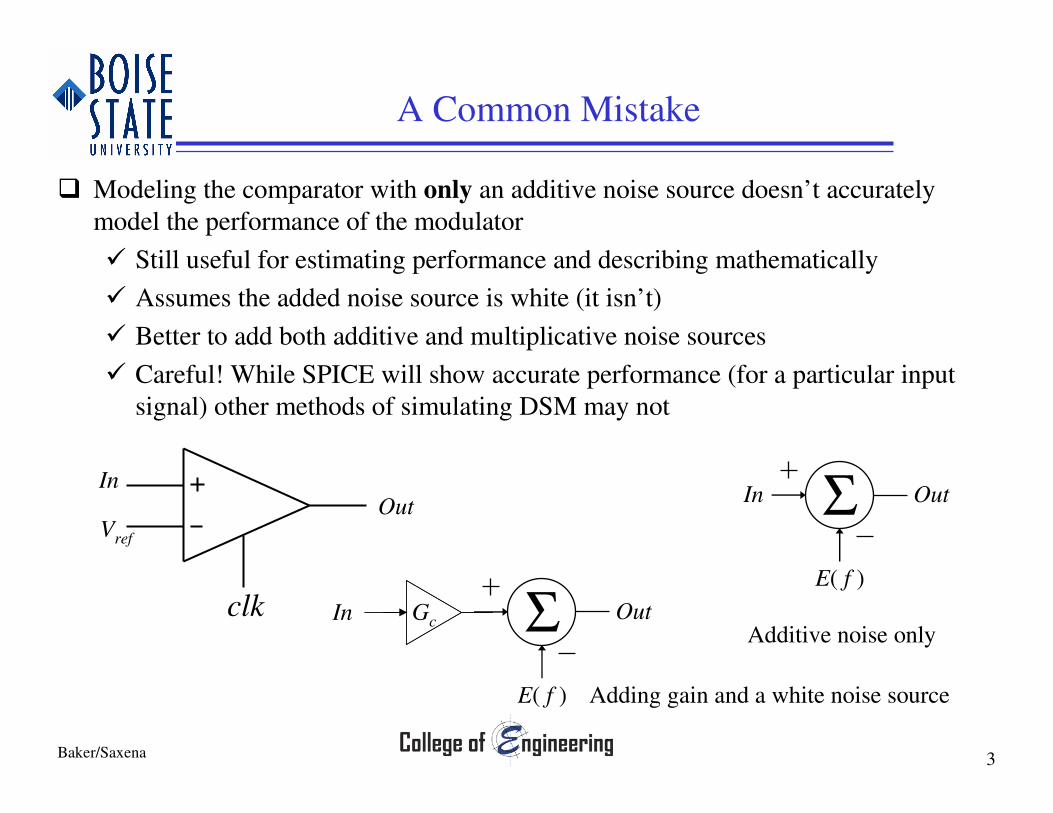
� Modeling the comparator with only an additive noise source doesn’t accurately
model the performance of the modulator
� Still useful for estimating performance and describing mathematically
� Assumes the added noise source is white (it isn’t)
� Better to add both additive and multiplicative noise sources
� Careful! While SPICE will show accurate performance (for a particular input
signal) other methods of simulating DSM may not
A Common Mistake
clk
Vref
InOut
Σ Out
E( f )
GcIn
Adding gain and a white noise source
ΣIn Out
E( f )
Additive noise only

Baker/Saxena 4
� Notice that this equation was derived assuming G1 and G2 are unity
(and they are likely < 1 to keep the integrators from saturating)
� Re-derive the transfer function adding a comparator gain and see that
forward (STF) gain goes to 1 and this equation is valid
Comments on low pass DSM transfer function
11
1−− z
1
1
1 −
−
− z
z
}
( )48476NTF
STF
zzEzzXzY211 1)()()( −− −⋅+⋅=

Baker/Saxena 5
Band Pass Delta-Sigma Modulation (BPDSM)
� A fourth order fs/4 band pass delta sigma modulator (BPDSM) can be
easily obtained by substituting −z−2 for z−1 in the low pass second
order DSM. The transfer function of the resulting band pass
modulator is given as (assuming G1= G2 = 1),
( ) ( )48476876
NTFSTF
zzEzzXzY222 1)()()( −− +⋅+−⋅=
21
1−+ z
2
2
1 −
−
+
−
z
z

Baker/Saxena 6
Redrawing the BPDSM topology
� Implementation of the BPDSM
� The next question we need to answer is how do we implement the
resonators?
� The problem is getting two delays for the feedback paths
21
1−+ z 2
2
1 −
−
+ z
z
Resonators
Phase shift

Baker/Saxena 7
Changing z−1 to z−2
� The integrator block in the low pass modulator becomes a resonator in
the equivalent band pass modulator topology. The low pass to band
pass modulator transformation can be understood as moving the pole
at 1 to +/− j. The modulation noise for the bandpass modulator can
now be written as 42
222cos2.
12)(.)(
=
ss
LSB
Qef
f
f
VfVfNTF π
-1.5 -1 -0.5 0 0.5 1 1.5
-1
-0.8
-0.6
-0.4
-0.2
0
0.2
0.4
0.6
0.8
1
Real Part
Imag
inary
Part
Pole/Zero Plot
z-plane for discrete integrator
0 0.1 0.2 0.3 0.4 0.5 0.6 0.7 0.8 0.9-10
0
10
20
30
40
50
60
70
Frequency (Hz)
Mag
nitu
de (
dB
)
Magnitude Response (dB)
Magnitude response for the integrator

Baker/Saxena 8
Changing z−1 to z−2, continued
-1.5 -1 -0.5 0 0.5 1 1.5
-1
-0.8
-0.6
-0.4
-0.2
0
0.2
0.4
0.6
0.8
1
Real Part
Ima
gin
ary
Part
2
Pole/Zero Plot
0 0.1 0.2 0.3 0.4 0.5 0.6 0.7 0.8 0.9-10
0
10
20
30
40
50
60
70
Frequency (Hz)
Magnitu
de (dB
)
Magnitude Response (dB)
Magnitude response of the resonatorz-plane for the resonators
� Below is the z-plane plot and magnitude response for z2/(z2 + 1)
Baker/Saxena 9
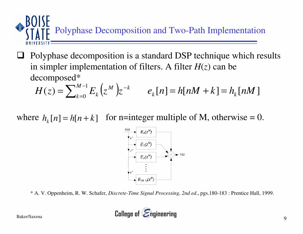
Polyphase Decomposition and Two-Path Implementation
� Polyphase decomposition is a standard DSP technique which results
in simpler implementation of filters. A filter H(z) can be
decomposed*
where for n=integer multiple of M, otherwise = 0.
* A. V. Oppenheim, R. W. Schafer, Discrete-Time Signal Processing, 2nd ed., pgs.180-183 : Prentice Hall, 1999.
][][][ nMhknMhne kk =+=
][][ knhnhk +=
( )∑−
=
−=1
0)(
M
k
kM
k zzEzH

Baker/Saxena 10
Changing z−1 to z−2, continued
� By using two paths we essentially double the sampling frequency.
� This changes z−1 to z−2
� Note that we are actually using fs/2 resonators!
11
1−+ z
1
1
1 −
−
+ z
z
11
1−+ z
1
1
1 −
−
+ z
z

Baker/Saxena 11
Frequency response of the sections
0 0.1 0.2 0.3 0.4 0.5 0.6 0.7 0.8 0.9-10
0
10
20
30
40
50
60
70
Frequency (Hz)
Ma
gnitu
de (
dB
)
Magnitude Response (dB)
0 0.1 0.2 0.3 0.4 0.5 0.6 0.7 0.8 0.9-10
0
10
20
30
40
50
60
70
Frequency (Hz)
Mag
nitu
de (
dB
)
Magnitude Response (dB)
Frequency response of 1/(1 + z−1),
note this is a high-pass response.
fs/2
Using two paths, 1/(1 + z−2), note
that this is a band pass response.
fs/4
Baker/Saxena 12
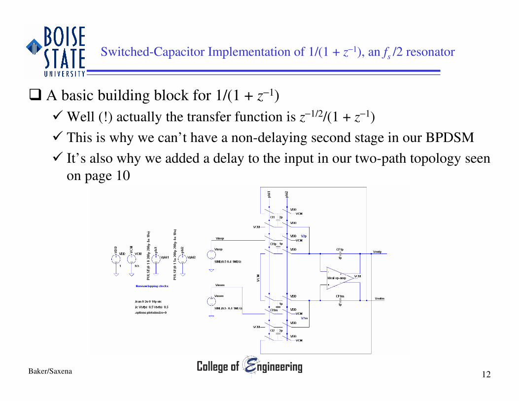
Switched-Capacitor Implementation of 1/(1 + z−1), an fs /2 resonator
� A basic building block for 1/(1 + z−1)
� Well (!) actually the transfer function is z−1/2/(1 + z−1)
� This is why we can’t have a non-delaying second stage in our BPDSM
� It’s also why we added a delay to the input in our two-path topology seen
on page 10
Baker/Saxena 13
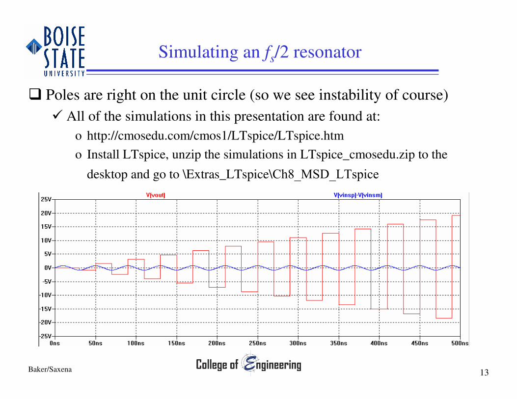
Simulating an fs/2 resonator
� Poles are right on the unit circle (so we see instability of course)
� All of the simulations in this presentation are found at:
o http://cmosedu.com/cmos1/LTspice/LTspice.htm
o Install LTspice, unzip the simulations in LTspice_cmosedu.zip to the
desktop and go to \Extras_LTspice\Ch8_MSD_LTspice

Baker/Saxena 14
Implementation of a BPDSM at fs/4

Baker/Saxena 15
Simulating Operation
� The band pass modulator shapes and moves the quantization noise
away from the IF at 25MHz. We can observe spurious tones for an
input of 25MHz. These tones are due to the limit cycle oscillations in
the system (just like applying a DC signal to a low pass modulator).Input at 25 MHz
Modulation noise
Baker/Saxena 16
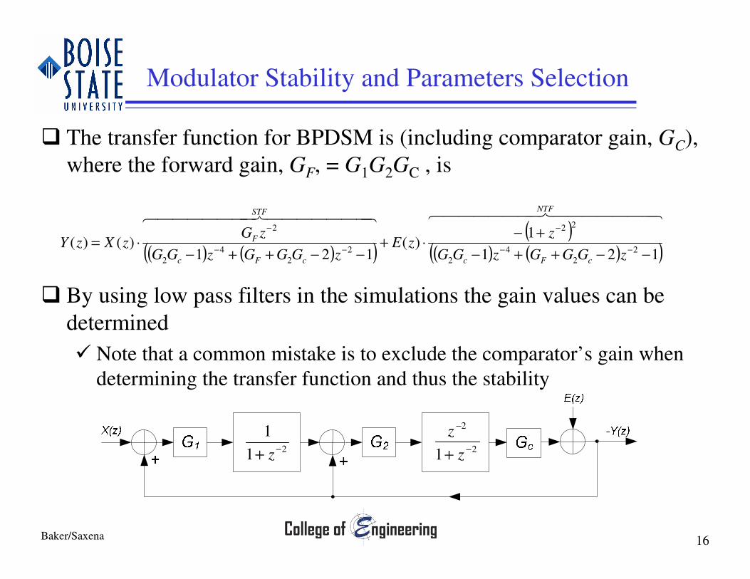
� The transfer function for BPDSM is (including comparator gain, GC),
where the forward gain, GF, = G1G2GC , is
� By using low pass filters in the simulations the gain values can be
determined
� Note that a common mistake is to exclude the comparator’s gain when
determining the transfer function and thus the stability
Modulator Stability and Parameters Selection
21
1−+ z 2
2
1 −
−
+ z
z
( ) ( )( )( )
( ) ( )( )
4444444 84444444 764444444 84444444 76NTF
cFc
STF
cFc
F
zGGGzGG
zzE
zGGGzGG
zGzXzY
121
1)(
121)()(
2
2
4
2
22
2
2
4
2
2
−−++−
+−⋅+
−−++−⋅=
−−
−
−−
−

Baker/Saxena 17
� Using two delaying resonators is a common mistake found in the literature!
� Adding gratuitous delay in the forward or feedback paths of a feedback system
makes the system move towards instability
� The difference between a delaying and non-delaying resonator is simply a
switch in the clock phases (swap the clock connections in the stage)
� This, using a delaying first stage, is also a common mistake found in the
literature covering the design of low pass delta-sigma modulators
� Note that it can be shown, both mathematically and with SPICE simulations,
that a modulator using a cascade of two delaying resonators is impossible to
make stable (so be careful when looking at the published literature!)
A Common Mistake
21
1−+ z 2
2
1 −
−
+ z
z
Using z−2 here in the numerator is bad!!!

Baker/Saxena 18
Digital I/Q Demodulation
� The band pass modulator can be used for fully digital I/Q
demodulation in a heterodyne receiver
� In the examples here the intermediate frequency, IF,= fs/4, is 25Mhz
� For this case, the mixing operation is very simple and can be
accomplished using some simple digital logic
Baker/Saxena 19
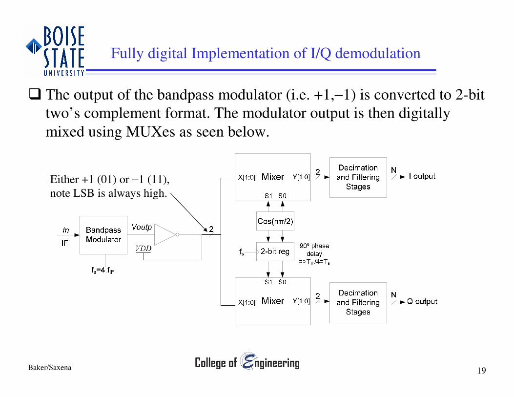
Fully digital Implementation of I/Q demodulation
� The output of the bandpass modulator (i.e. +1,−1) is converted to 2-bit
two’s complement format. The modulator output is then digitally
mixed using MUXes as seen below.
Either +1 (01) or −1 (11),
note LSB is always high.

Baker/Saxena 20
Digital Mixer Implementation using Selectors (aka MUXes)
� The output of the reference generator is, cos(2πfIFnTs) = cos(nπ/2) = 1, 0, −1, 0, ...
sequence, which in 2’s complement format is 01, 00, 11, 00, …sequence.
� Note that the point of doing digital I/Q demodulation is that we move the digital data
down to a low frequency (for a general communication system, like transmission of
voice, this may be in the kHz range)
� Low power can thus be obtained and DSP can be used
Baker/Saxena 21
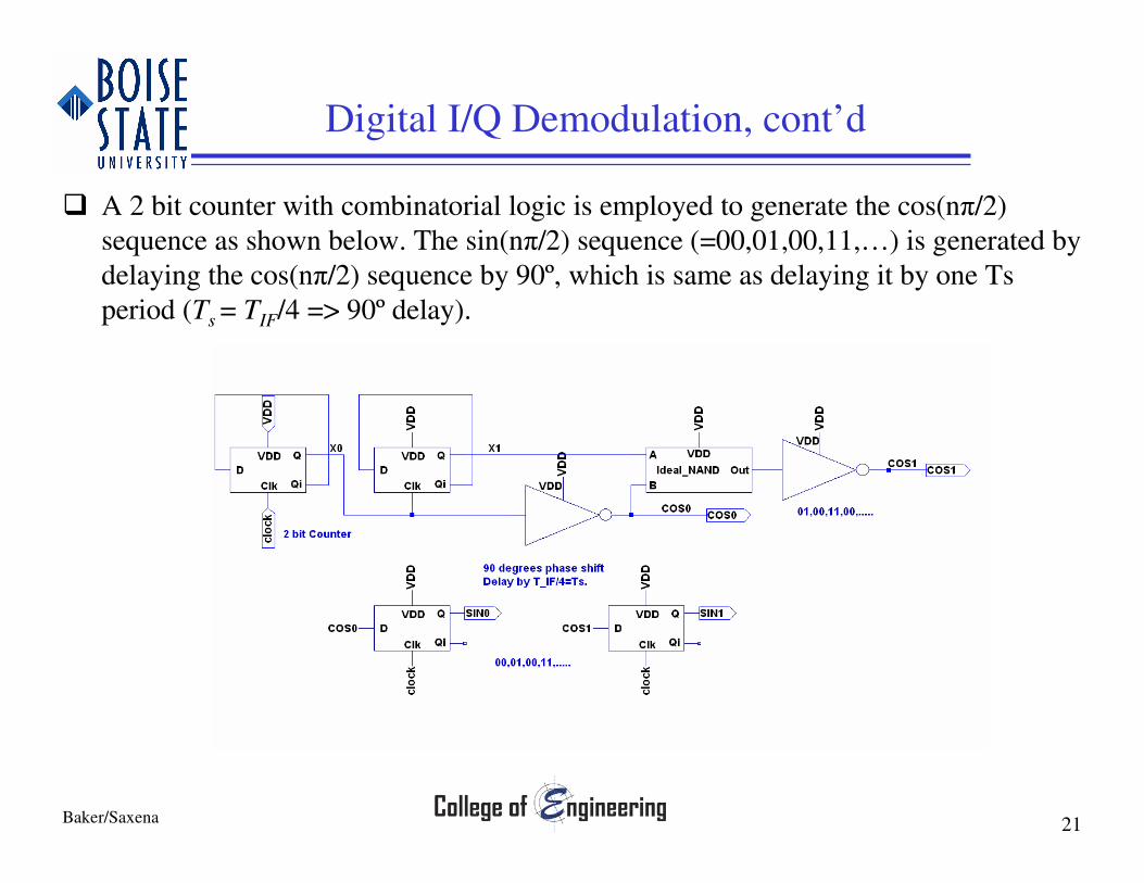
Digital I/Q Demodulation, cont’d
� A 2 bit counter with combinatorial logic is employed to generate the cos(nπ/2)
sequence as shown below. The sin(nπ/2) sequence (=00,01,00,11,…) is generated by
delaying the cos(nπ/2) sequence by 90º, which is same as delaying it by one Ts
period (Ts = TIF/4 => 90º delay).
Baker/Saxena 22
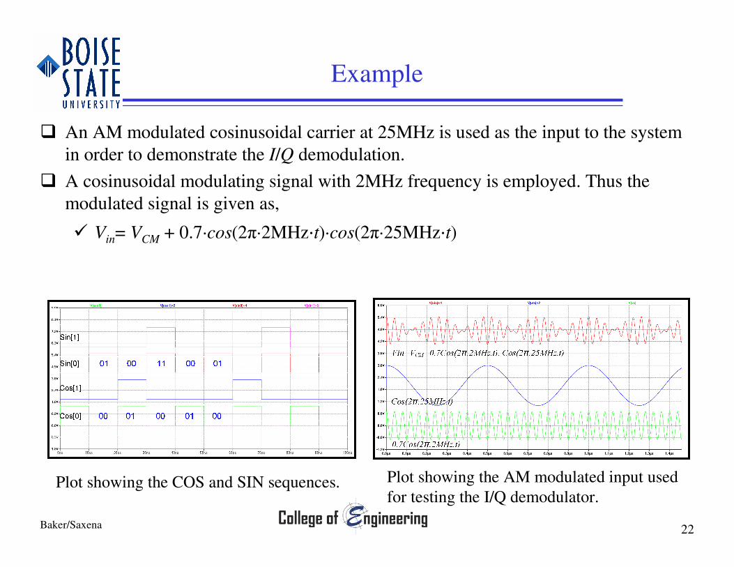
Example
� An AM modulated cosinusoidal carrier at 25MHz is used as the input to the system
in order to demonstrate the I/Q demodulation.
� A cosinusoidal modulating signal with 2MHz frequency is employed. Thus the
modulated signal is given as,
� Vin= VCM + 0.7·cos(2π·2MHz·t)·cos(2π·25MHz·t)
Plot showing the COS and SIN sequences. Plot showing the AM modulated input used
for testing the I/Q demodulator.

Baker/Saxena 23
� An I/Q modulated signal is described as
s(t) = Ac · [mI(t) · cos(2πfct) + mQ(t) · sin(2πfct)]
� Here the I component is mI(t)= 0.7·cos(2π·2MHz·t) and the Q component, mQ(t), is 0 (a DC
voltage of VCM=0.75V).
� Below is an example where we’ve used a modulating signal of 100 kHz (instead of 2 MHz)
� The bottom trace, the I component, shows both the modulated carrier and the final 100
kHz output after filtering (the Q component output is a DC voltage of 0.75 V)
Example, cont’d
Vin
BPM
output
I output
Q output
100KHz cosine

Baker/Saxena 24
Example, cont’d
� Showing the spectrums of the signals at various points in our receiver.
� Note the carrier is 25 MHz and the information is offset from the carrier
by 100 kHz (here 24.9 and 25.1 MHz)
� Note how the in-phase component is shifted down to DC.

Baker/Saxena 25
Showing the Signal in the Baseband
� Seen below is a close up view of the I output component seen on the
previous slide
� Note that the digital data is still moving at full speed!
� Still need to decimate (reduce the digital clocking frequency)
� Prior to decimating we need to pass the data through digital anti-aliasing
filters
o It’s important for low power operation to keep things as simple as possible
Baker/Saxena 26
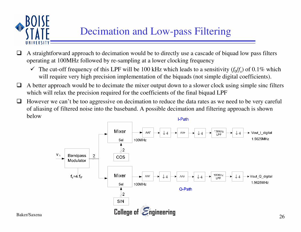
Decimation and Low-pass Filtering
� A straightforward approach to decimation would be to directly use a cascade of biquad low pass filters
operating at 100MHz followed by re-sampling at a lower clocking frequency
� The cut-off frequency of this LPF will be 100 kHz which leads to a sensitivity (f0/fs) of 0.1% which
will require very high precision implementation of the biquads (not simple digital coefficients).
� A better approach would be to decimate the mixer output down to a slower clock using simple sinc filters
which will relax the precision required for the coefficients of the final biquad LPF
� However we can’t be too aggressive on decimation to reduce the data rates as we need to be very careful
of aliasing of filtered noise into the baseband. A possible decimation and filtering approach is shown
below
4↓ 4↓ 4↓
4↓ 4↓ 4↓
Baker/Saxena 27
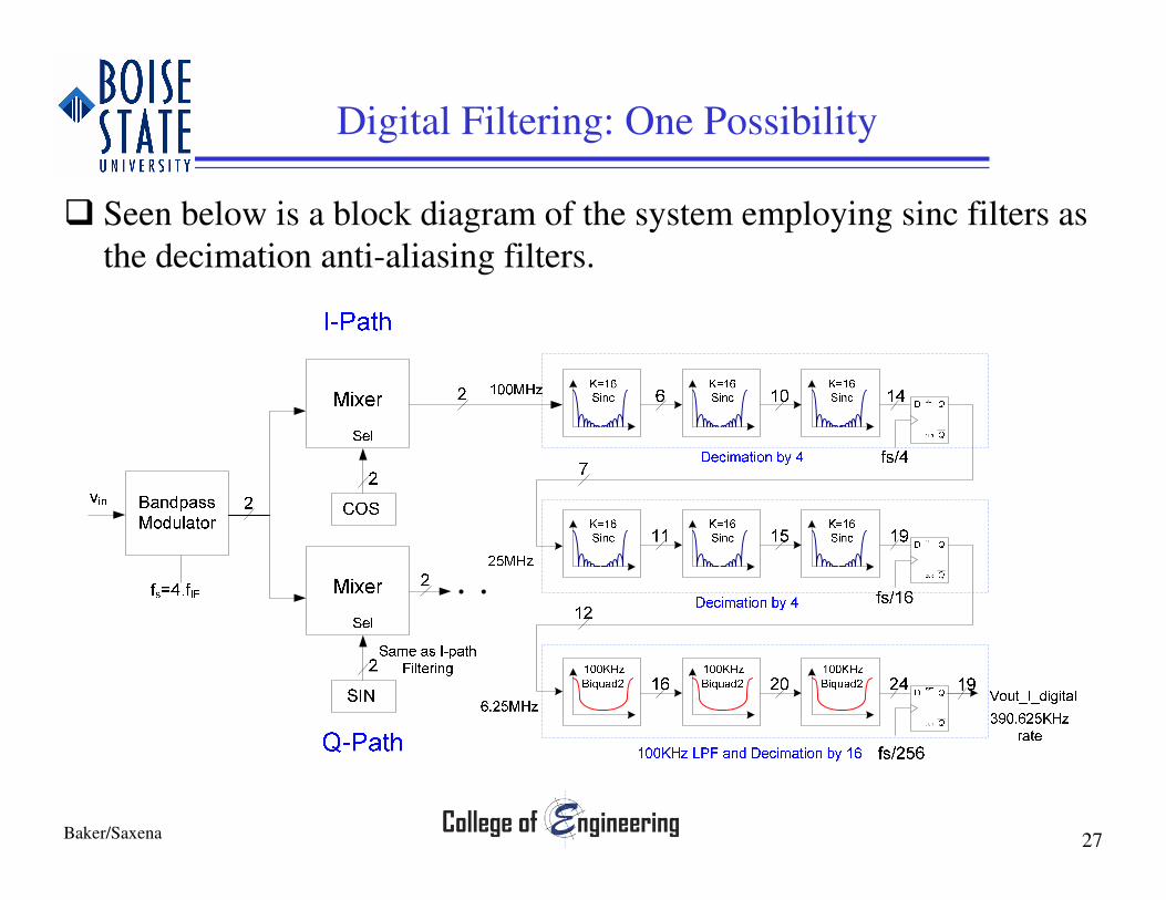
Digital Filtering: One Possibility
� Seen below is a block diagram of the system employing sinc filters as
the decimation anti-aliasing filters.
Baker/Saxena 28
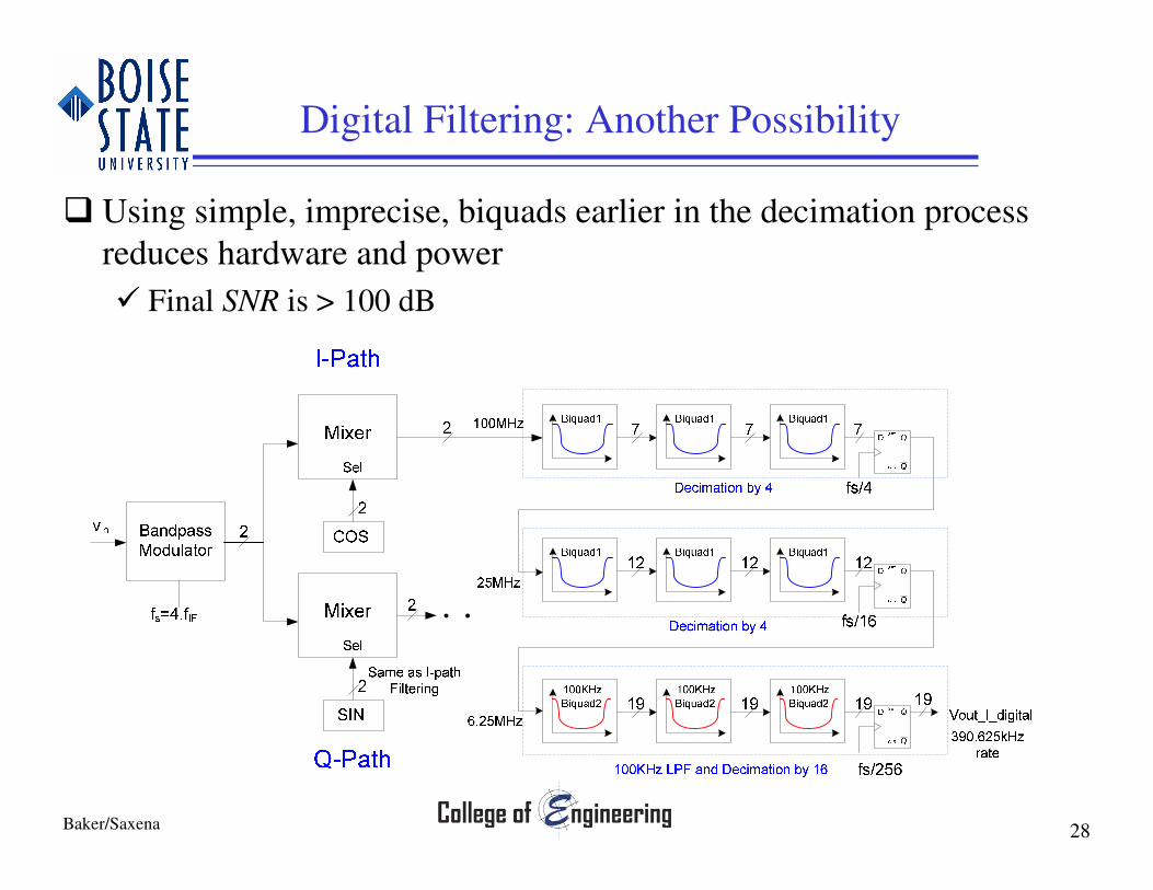
Digital Filtering: Another Possibility
� Using simple, imprecise, biquads earlier in the decimation process
reduces hardware and power
� Final SNR is > 100 dB
Baker/Saxena 29
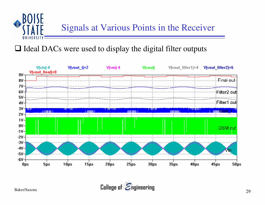
Signals at Various Points in the Receiver
� Ideal DACs were used to display the digital filter outputs

Baker/Saxena 30
Conclusions and Research Directions
� We’ve talked about the implementation of band pass delta-sigma
modulators (BPDSM) for use in heterodyne receivers
� Some common mistakes made when designing BPDSM were
presented and discussed
� Concerns for implementing the digital filtering were discussed
� Research directions include:
� Low power using passive implementations
o Continuous-time circuits using both passive and simple active
implementations are clearly of future importance
� Parallel paths (> 2) to effectively increase SNR
o Reduces the effects of clock jitter
� Of course the digital filtering is important for both power and size