design of current mode signal processing circuit using ... · design of current mode signal...
TRANSCRIPT
Available online www.ejaet.com
European Journal of Advances in Engineering and Technology, 2015, 2(8): 21-43
Research Article ISSN: 2394 - 658X
21
Design of Current Mode Signal Processing Circuit using Current Differencing Transconductance Amplifier
Shalini Chaudhary1, Vinod Kumar Nirala 2, Sanjay Singh1, Pankaj Punia1 and Dheeraj Kumar3
1Department of Electronics and Communication Engineering, Uttaranchal University, Dehradun, India
2Department of Electronics and Communication Engg., Uttarakhand Technical University, Dehradun, India 3Department of Biotechnology, Graphic Era University, Dehradun, India
[email protected] _____________________________________________________________________________________________
ABSTRACT Frequency filters are linear electric circuits that are used in wide area of electronics. They are also the basic building blocks in analogue signal processing. In the last decade, a huge number of active building blocks for analogue signal processing were introduced. However, there is still the need to develop new active elements that offer new possibilities and better parameters. The current, voltage or mixed-mode analog circuits and their various aspects are discussed in the Paper. This work reflects the trend of low-power (LP) low-voltage (LV) circuits for portable electronic and mobile communication systems and the problems of their design. The need for high performance LV circuits encourages the analog designers to look for new circuit Architectures and new LV techniques. This paper presents a high-performance current differencing transconductance Amplifier (CDTA), a recently reported active element, especially suitable for analog signal processing applications. A high linearity CMOS configuration for a CDTA is made up of high linearity input and output stages. It is a resistor less circuit, so it is beneficial to IC implementation in terms of space consideration. The circuit is a second order single input multiple output (SIMO) current-mode filter. This filter can simultaneously realize all basic filter functions high pass, low pass and band pass Responses without any component-matching conditions. All the active and passive sensitivities are low presents a voltage-mode universal filter using a CDTA. It has two inputs and one output. The circuit can simultaneously realize low-pass, band pass, and high pass, band reject and all pass filter functions without changing the circuit topology and passive elements. A voltage-mode Oscillator using CDTA is presented, in which Oscillator has high input impedance and employs four active elements, two grounded capacitors and there is no resistor. Based on the generalized description of the structure various solutions are presented and compared. Universal filter, Adder, Integrator, Second order butterworth filter these circuits are designed in Tanner tool and all results are verified with the help of T Spices imulation results are Included to verify and demonstrate the feasibility of the Oscillator. All the simulation Results using a TSMC 0.35-μm CMOS process model were included to verify the Expected values.
Key words: CMOS based CDTA, Differencing transconductance amplifier, butterworth filter integrator & adder, universal filter _____________________________________________________________________________________
INTRODUCTION
Filters are widely used in analog signal processing to select the particular frequency. Voltage-mode and current-mode circuits such as current conveyors and current feedback operational amplifiers are getting much attention as compared to other active elements due to wider bandwidth, simple circuitry, low power consumptions and dynamic ranges. In the last decade, a huge number of active building blocks were introduced for analogue signal processing. However, there is still the need to develop new active elements that offer new and better advantages. This thesis is, therefore, focused on definition of other novel analog building blocks and, furthermore, novel filter structure designs. In the present days, a number of trends can be noticed in the area of analogue filter and oscillator design, namely reducing the supply voltage of integrated circuits and transition to the current-mode. On the other hand, current-, voltage- and mixed-mode analog circuits design still receives considerable attention of many researches.
In order to increase the speed of circuits for analog signal processing and to decrease the supply voltages of integrated circuits, designers devote their attention to the so-called current mode. It means – simply speaking – that

Chaudhary et al Euro. J. Adv. Engg. Tech., 2015, 2(8):21-43 _____________________________________________________________________________________________
22
the individual circuit elements should interact by means of currents, not voltages. In practice, we can only approach the current mode because a current flowing through circuit element necessarily causes a voltage drop. Choosing proper impedance levels, sufficiently small voltages can be achieved with the aim to eliminate the influence of Miller’s capacitances and other non-idealities. The starts from the idea of a circuit that consists of active elements, whose input and output signals are currents, from passive C or R elements which are connected to these active blocks in the defined, from the point of view of small voltages „watched’ nodes, and from current differencing transconductance amplifier (CDTA) which transfer the given voltages back into currents. The analog filters are mostly used in high speed data communication for signal processing in cable modems, regulation and measurement techniques in electro acoustic applications. The circuits based on current-mode technique are suited for these applications. Nowadays, the applications and advantages in the realization of various active transfer functions, called as universal biquad filters, have received considerable attention. A universal filter may be used in phase locked loop FM stereo demodulators, and crossover networks used in three-way high fidelity loudspeakers. However, a current-mode universal filter has being been more popular than voltage-mode one. This is due to operating in low-voltage environment as in portable and battery powered equipment. Since a low-voltage operating circuit becomes necessary, the current-mode technique is ideally suited for this purpose more than the voltage-mode one. Presently, there is a growing interest in synthesizing the current-mode circuits because of more their potential advantages such as larger dynamic range, higher signal bandwidth, greater linearity, simpler circuitry and lower power consumption.
During the last two decades, research in the field of analog CMOS circuits has gained a lot of interest. Continuous improvements in CMOS technology enabled the integration of (largely digital) complete electronic systems on a single chip. Usually, analog and mixed analog-digital circuits are now found at the interface of such systems with the ‘analog real world’. Furthermore, analog signal processing can be favorable in terms of speed, chip area and power dissipation, especially for low and moderate precision circuits. Linear circuits, like amplifiers and filters, are indispensable analog building blocks. Their properties often critically determine system performance. In order to achieve high performance, circuits are usually designed in such a way, that the transfer function is mainly determined by a few carefully chosen components. Passive components, especially resistors and capacitors, are predominantly used for this purpose. In this approach, active devices like MOS transistors are used to provide sufficient gain. Ideally, they do not influence the transfer function. The underlying motivation is that passive devices are superior with respect to e.g. linearity, accuracy and noise. Although the use of passive components is preferable in many cases, there are also drawbacks. A major one is that electronic control of the value of these components is hardly possible. Such control is often desired in order to compensate for deviations from nominal component values due to fabrication tolerances, temperature variations and ageing. Without self-correction, these deviations will change the transfer function of linear circuits, e.g. resulting in a shift of the pass-band of a filter. Moreover, electronic control of the transfer function is needed in applications with varying signal conditions, e.g. to handle signals with a variable signal amplitude or frequency content. Of course, it is possible to change the value of passive components in discrete steps, e.g. by means of MOS transistor switches. However, if the required resolution is high, this approach becomes impractical. Furthermore, the resistance of the switches often introduces problems and finally, the switching transients may give problems with full continuous-time signal processing.
Operating System and EDA Tools used The operating system and EDA Tools used in thesis are as follows:
Operating System Windows XP
Tool
Tanner EDA Tool S-Edit
T-Spice Pro W-Edit
L-Edit Pr CMOS BASED CDTA
This section introduces the reader with the CDTA (Current Differencing Transconductance Amplifier). As conversation continues, a design method of the CMOS based CDTA with several conditions is discussed. This segment also includes the simulation results of CDTA.
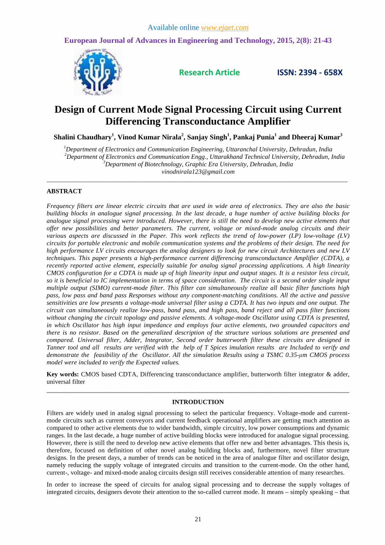
A CDTA consists of an input current differencer and a dual output transconductance stage as shown in Fig.1. The input stage takes the difference of input signals and transfers this difference current to the intermediate z terminal, where this current is converted to voltage via external impedance. A CDTA is a 5-terminal current-mode active building block [9]. It can be also considered as a current operational amplifier, as in Fig.2 (a), and the defining Eqns matrix is given in Fig.2 (b) [25], [21].
Chaudhary et al Euro. J. Adv. Engg. Tech., 2015, 2(8):21-43 _____________________________________________________________________________________________
23
VVII = 0010 00−10 0000 000±gm IIVV
The Eqns derived from the matrix is given below Vp = Vn = 0 (1) Iz = Ip – In (2)
Ix+ = +gmVz (3)
Ix- = -gmVz (4) Considering the deviation of the voltage and current gains from their ideal values, the defining Eqn of the CDTA in Fig.2 (b) becomes:
VVII = 00
α0 00−α0 0000 000±gm IIVV
The modifiefd Eqns are given below Vp = Vn = 0 (5) Iz = αp Ip – αn In (6)
Ix+ = +gmVz (7)
Ix- = -gmVz (8) Where αp and αn are current gains, αp= 1 – εp and αn= 1 – εn. Hence εp and εn are the current tracking errors, and their absolute values are much less than the unit value.
Fig.1 CMOS Description of CDTA
This device, with 2 current inputs and 2 kinds of current output, provides an easy implementation of current-mode active filters. A CDTA is a synthesis of the well-known advantages of the current differencing amplifier and a transconductance amplifier to facilitate the implementation of current-mode active filters [19-26]. The main features of a CDTA are low gain errors (high accuracy), high linearity, high transconductance, and wide frequency response. In addition, high output resistance at terminal X of the CDTA is required to enable easy cascading without the need for additional active elements in applications. The circuit exhibits low output resistance and limited linearity range, which causes deviations in the expected performance of the application circuits employing the CDTA. Improved CMOS configuration of a CDTA is providing low input impedances at ports p and n, very high output impedances at ports z and x, an extended linearity range, and high transconductance. To provide high output impedance values, cascode current mirrors and regulated cascode current mirrors were used in the CDTA structure. Furthermore, the input linearity range of the transconductor section was increased by introducing a cross-coupled configuration. The Current Differencing Transconductance Amplifier (CDTA) is the active element operating in current-mode and can be applied to various circuits such as comparators, second order high pass, second order low pass, second order band pass filters. The differential input current flows over the z terminal. External impedance is usually connected to this node and the voltage over this impedance is converted to the output currents by the output transconductors with transconductance gm for the positive output and -gm for the negative output. The CDTA is free from parasitic input capacitances and it can operate in a wide frequency range due to current mode operation. Some voltage and current mode applications using this element have already been reported in literature.
According to above Eqn and the circuit of Fig.2 (a), the current through terminal z follows the difference of the currents through the terminals p and n (Ip− In), and flows into from terminal z impedance Zz. The voltage drop at

Chaudhary et al Euro. J. Adv. Engg. Tech., 2015, 2(8):21-43 _____________________________________________________________________________________________
24
terminal z is transferred to a current at terminal x (Ix) by a transconductance gain (gm), which is the electronically controllable by an external bias current. The Current Differencing Transconductance Amplifier (CDTA) is the active element operating in current-mode and can be applied to various circuits such as comparators, second order high pass, second order low pass, second order band pass filters.
(a)
(b) Fig.2 (a) CDTA Symbol (b) Behavioral Modal of CDTA [24]
DESIGN METHOD OF A CDTA
Required Parameters The subsequent design practice assumes that provisions for the following parameters are specified:
a) Unity gain bandwidth (GB) b) Load capacitance (CL) c) Range of Input common mode (Iin (min) and Iin (max)) d) Slew rate (SR) e) Power dissipation (Pdiss) f) Voltage swing of Output (Vout (min) and Vout (max)) g) Dc Gain (AV)
Table - 1 Transistors Aspect Ratios Simulation Circuit of CDTA Transistors W(µm) L(µm)
M1, M2 0.45 0.25
M3 1 1
M4, M5, M6, M10 1 0.25
M7, M8, M15, M16, M17, M18 10 0.25
M9, M19, M20 0.25 0.25
M11, M12, M13, M14, M21, M22, M23, M24 5 0.25
Fig.3 Schematic diagram of CDTA [24]

Chaudhary et al Euro. J. Adv. Engg. Tech., 2015, 2(8):21-43 _____________________________________________________________________________________________
25
Properties of CDTA The CDTA is free from parasitic input capacitances and it can operate in a wide frequency range due to current mode operation. Some voltage and current mode applications using this element have already been reported in literature, particularly from the area of frequency filtering: general higher-order filters, biquad circuits, all-pass sections, gyrators, simulation of grounded and floating inductances and LCR ladder structures. Other studies propose CDTA-based high-frequency oscillators. Nonlinear CDTA applications are also expected, particularly precise rectifiers, current-mode Schmitt triggers for measuring purposes and signal generation, current-mode multipliers, etc.
Basic Operation The CDTA element with its schematic symbol in Fig.3 has a pair of low-impedance current inputs and p, n and an auxiliary terminal z, whose outgoing current is the difference of input currents. Here, output terminal currents are equal in magnitude, but flow in opposite directions, and the product of transconductance (gm) and the voltage at the z terminal gives their magnitudes. Therefore, this active element can be characterized with the following Eqns [31].
Vp = Vn = 0 (9) Iz = Ip – In (10) Ix+ = gm.Vz (11)
Where Vz- = Iz.Zz and Zz is the external impedance connected to z terminal of the CDTA. CDTA can be thought as a combination of a current differencing unit followed by a dual-output current differencing transconductance amplifier, DO- CDTA. Ideally, the CDTA is assumed as an ideal current controlled current source and can be described by Ix+ = gm.Vz and Ix- = -gmVz, where Ix+ and Ix- are the output currents, Vz denot external added terminal voltage of CDTA, respectively. Note that gm is a function of the bias current. When this element is used in CDTA, one of its input terminals is grounded. With dual output availability, Ix+ = -Ix- condition is assumed. These currents, which are copied to a general number of output current terminals x, are equal in magnitude but flow in opposite directions.
The (CDTA) is composed of a unity-gain current source controlled by the difference of two input currents and a multi-output transconductance amplifier providing electronic tuning ability through its transconductance gain (gm). Therefore, this device is quite suitable for the synthesis of current-mode filters with electronically tenability properties. Moreover, the use of the CDTA as an active element provides the circuit implementations with a reduced number of passive elements, thereby leading to compact structures in some applications. All these advantages together with its current-mode operation nature make the CDTA a promising choice for implementing the current-mode continuous-time signal processing circuits consecutively.
Assuming that transistors PMOS_5 and NMOS_5 are working in their saturation regions, the transconductance gain (gm) can be expressed as [31].
gm = µCox Ib (12)
where µ and Cox are the carrier mobility and the gate oxide capacitance per unit area, respectively. W is the effective channel width and L is the effective channel length. From Eq. (1.4), it can be shown that the transconductance gain of the CDTA can be electronically controlled by adjusting bias current Ib. Other studies propose CDTA-based high-frequency oscillators. Nonlinear CDTA applications are also expected, particularly precise rectifiers, current-mode Schmitt triggers for measuring purposes and signal generation, current-mode multipliers, etc. CDTA applications do not require the use of external resistors, which are substituted by internal transconductors. Analogously to the well-known ‘gmC’ applications, the ‘CDTA-C’ circuits are formed by CDTA elements and grounded capacitors. Such structures are well-suited for on-chip implementation.
Layout of CDTA The physical layout of error amplifier has been designed using UMC 0.18μm CMOS process technology in cadence virtuoso layout editor. Design Rule Check (DRC) is performed in order to verify that layout fulfills all electrical and geometric rules provided by foundry. The basic design rules are:
Metal 1 to metal 1 spacing 0.24 μm Diffusion contact to poly spacing 0.15 μm Minimum contact size 0.24 μm, 0.24 μm Minimum p+ implant overlap p+ diffusion 0.22 μm Poly to poly spacing 0.24 μm Poly width 0.18 μm Poly to metal spacing 0.28/0.00 μm Minimum poly extension on to field region 0.22 μm
Contact overlap to p+ diffusion 0.1 μm Poly contact to diffusion edge spacing 0.18 μm Metal 1 width 0.24 μm Minimum poly overlap contact 0.1 μm
Poly extension beyond active 0.22 μm Minimum metal area 0.1764 μm2
Minimum contact spacing 0.26 μm N well overlap p+ diffusion 0.43 μm

Chaudhary et al Euro. J. Adv. Engg. Tech., 2015, 2(8):21-43 _____________________________________________________________________________________________
26
Fig.4 Layout diagram of CDTA
Fig.5 Verification of Layout of CDTA using DRC rule

Chaudhary et al Euro. J. Adv. Engg. Tech., 2015, 2(8):21-43 _____________________________________________________________________________________________
27
Fig.6 Current transfer from p and n to z
Fig.7 Variation of z terminal current (Ip parametri c)
Analysis of Simulated Result of CDTA The input terminals current transfer characteristics are shown in Fig.6, obtained when one input is open-circuited (Ip = 0). The input stage transfers the difference of the input currents to the z terminal with good accuracy, as demonstrated in the Fig.3 Since few internal nodes exist over the signal path from the input to the z terminal of the input stage, and high frequency operation is satisfied, exploiting the high frequency capability of current mode signal processing. For the further characteristics of CDTA we can see the variation at z terminal current to the input current if we make the value of Ip parametric. Variation of the dual output transconductance stage’s output currents with respect to the input current is given in Fig.7.

Chaudhary et al Euro. J. Adv. Engg. Tech., 2015, 2(8):21-43 _____________________________________________________________________________________________
28
BUTTERWORTH FILTERS INTEGRATOR & ADDER
In this chapter the reason behind study on Active – RC Butterworth filter are described. The design ladder for the design of Active-RC Butterworth filter is discussed afterwards in this chapter. Further, design with simulations and results of 6th order active-RC Butterworth filter are explained. The different orders of filters are designed, simulated and analyzed in term of pass-band frequency.
Second order Butterworth Filter Active filters are mostly used in communication and signal processing circuits. They are also engaged in a broad range of applications such as medical electronics, etc. Most commonly used active filters. A second order filter can be obtained by coupling two first order active filters; a second order filter can be obtained simply by introducing an additional RC network in the first order filter as shown in Fig. 8. Second order filters are important because higher order filters designed using them.
The filters can be Design by means of operational amplifier as the active element and capacitors and resistors as the passive elements (frequency discriminating part). Improved filter performance is obtained by employing op-amps with superior slew rates and superior gain bandwidths. The filtering application of the circuit is finest represent by the frequency response parameters of the circuit, which define the dissimilarity of the filter circuit gain with admiration to operating frequency [41].
There are a lot of filter approximations that have been used for the filter design. One of the improved used is the Butterworth approximation. Butterworth filter is a category of electronic filter characterized by showing a maximally smooth magnitude response, i.e., no ripple in amplitude of the pass-band. [Difference with Chebyshev] This circuit is depends upon Butterworth transfer functions (or Butterworth polynomials). [For the mathematically disposed, these polynomials stand for a specialized solution to a common Mac Laurin series based upon Taylor series expansion. The filter was named after a British engineer S. Butterworth, who originally shows this response in his research paper ‘On the Theory of Filter Amplifiers’, Wireless Engineer, After Eleven years, Landon present the maximally flat response in his paper ‘Cascade Amplifiers through Maximal Flatness’.
Properties of Butterworth Filter Essential properties of Butterworth filter (these properties are appropriate for all other filters with dissimilar responses):
Filter Order The filter order is important for several reasons. It is straight correlated to the amount of components use in the filter, and for that reason to its physical size, its cost, and the difficulty of the design task. Thus, higher-order filters are further expensive, take up extra space, and are additional tricky to design. The major advantage of a higher order filter is that it gives a steeper roll off slope than a like lower-order filter.
Ultimate Roll off Rate The roll off of Butterworth filter is smooth and monotonic, frequently expressed as the quantity of attenuation in dB for a given ratio of frequencies. The most general units are ‘dB/decade’ and ‘dB/octave’. The ultimate roll off rate must be 20 dB/decade for each filter pole in the statement of a high-pass or low-pass filter and 20 dB/decade for each couple of poles for a band-pass filter, some of those filters will have steeper attenuation curve near the cut-off frequency than others of the similar order.
Attenuation Rate close to the Cut-off Frequency If filter is intended to eliminate a signal very near in frequency to a signal that must be passed, a prickly cut-off characteristic is attractive between those two frequencies.
Transient Response Curve of amplitude response described how a filter response to steady-state with input signals of sinusoidal type. Since a real filter will have far more composite signals apply to its input ports, it is often of attention to know how it will behave below transient circumstances. An input signal made of a step function provides a good indication.
Monotonicity If filters gain slope never changes its sign then its amplitude response called monotonic. In other ways, if with increasing frequency gain always increases or increasing frequency gain always decreases. Perceptibly, this can show only in the response of a high-pass or low-pass filter. Monotonic on both side of the centre frequency can be shown by band pass filter.
Pass-band Ripple Butterworth filters have a very plane pass band with no magnitude ripples. If within its pass-band a filter is not monotonic, the transfer function within the pass-band will show off one or extra ‘bumps’. These bumps are recognized as ‘ripple’. Some application doesn’t necessarily require monotonicity, but do necessitate that the pass-

Chaudhary et al Euro. J. Adv. Engg. Tech., 2015, 2(8):21-43 _____________________________________________________________________________________________
29
band ripple exist limited to some greatest value (typically 1 dB or less). Although band-pass and band-reject filters do not have monotonic transfer functions, they exposed a free of ripple within their pass-bands.
Stop-band Ripple Some of the filter characteristics also have ripple in the stop-bands. We are frequently undisturbed about the quantity of ripple in the stop-band, as long as the signal to be discarded is adequately attenuated. It Shows that the ‘ideal’ filter amplitude output curves are not actually realizable, we must choose a suitable approximation to the ideal response. The word ‘suitable’ may have diverse meanings in diverse situations. The satisfactoriness of filter architecture will depend on numerous consistent factors, counting the amplitude response characteristics, transient response, and physical size of the circuit and cost of implementing the design.
Pass Band Gain Using active filters, it is probable to realize a pass band gain superior than 1. Mainly active filters utilize an amplifier, which determine the pass band gain of the filter. Filters with a flat pass-band gain are frequently used, and such a response is providing by Butterworth filters. A different class of filters known Chebyshev filters, offer a ripple (or overshoots in) pass-band gain.
Second Order Filters Second order filters offer -40 dB/decade roll-off in the stop-band and hence achieve better frequency choice than the first order type. Using second order, or higher-order filters, we can get attractive frequency responses. Consider the two frequency responses shown in Fig.8.
Fig.8 Second Order Low Pass Responses
Butterworth filters give us a realistically flat gain in the pass-band, while the Chebyshev filters give a ripple or overshoot in the frequency response. The trade-off is that at the cut-off frequency, Chebyshev filter shows a higher roll-off rate. These frequency response types are determined the damping factor of the filter circuits.
Damping Factor The damping factor (DF) of an active filter Design described which response characteristics the filter exhibits -whether, Butterworth or Chebyshev or others. The damping factor is provided by the negative feedback Design and is defined by the following Eqn:
DF = 2 - (13)
To achieve a second-order Butterworth response, for example, the damping factor must be 1.414. Therefore, to implement this damping factor, the feedback resistor ratio must be = 2 – DF = 2 – 1.414 = 0.586 (14)
Hence, for a second-order Butterworth response, RF = 0.586 R1.
SECOND ORDER LOW PASS BUTTERWORTH FILTER
A second order low-pass filter provides a - 40 dB/decade roll-off rate [22] in the stop-band. The first order low-pass filter can be converted into a second-order type simply by using an additional RC network (as shown in Fig. 9). A second order filter can be obtained by adding a RC network in the first order filter, second order filters are important because higher order filter designed using them. Butterworth filters give us a realistically flat gain in the pass-band, while the Chebyshev filters give a ripple or overshoot in the frequency response. The trade-off is that at the cut-off frequency, Chebyshev filter shows a higher roll-off rate. These frequency response types are determined the damping factor of the filter circuits.
The circuit shown in Fig.9 is also called a two pole low paas filter because it has two bypass circuits. The two pole of this circuit modify the cut off frequency and the response of the circuit. The gain of the filter is set by R1 and RF, while the high cut-off frequency (fh) is set by RA, CA, RB and CB as follows:

Chaudhary et al _____________________________________________________________________________________________
fh =
| !"# $% | =
Where Af = (1+Rf/R1), the pass-band gain of the filter, f is the frequency of input signal icut-off frequency in Hz.
A second order filter can be obtained by coupling two first order active simply by introducing an additional RC network in the first order filter as shown in 40 dB/decade roll-off in the stop-band and hence achieve better frequency choice than the first order type. Using second order, or higher-order filters, we can get attractive frequency responses. Second order filters are because higher order filters designed using them. The designing of second order lowin Fig.9.
DESIGN PROCEDURE TO DESIGN ACTIVE
The steps used to design an active-RC Butterworth filter are as follows:• An active device is selected for the filter. It may be an op
(DDA) or second generation current• The conditions for the design of active device are laid down giving an importance on the UGB, the supply
voltages used and power dissipation. The design steps for CDTA have been shown in above.• The active device should be design according to the specifications. Simulate the schematic
and check performance of it. • At last lay down specifications for filter. The filter design process starts with the filter user specifying the
transmission characteristics necessary for the filter. A low pass filter transmission is chparameters:
The maximum approved variation in pass The pass-band edging The minimum requisite stop The stop-band edging
• Compute for which order of filter the design can be considered if the four parameters shown above are given. Transfer function of the Butterworth filter can be computed subsequently. The Butterworth lowzeros at ω = ∞, building it an all pole filter. The magnitude function for an Nth order Butterworth filter with a pass-band edge ωp is specified by
|T(jω)| =
At ω = ω
|T(jω)| =
So, the parameter ε calculated the maximum deviation in pass
Amax = 20log
As per the specifications and the transfer function, the determination of order can be in following steps:
Euro. J. Adv. Engg. Tech., 201_____________________________________________________________________________________________
30
&'()')(
| = *
+&,- ./0
band gain of the filter, f is the frequency of input signal i
A second order filter can be obtained by coupling two first order active filters; a second order filter can be obtained simply by introducing an additional RC network in the first order filter as shown in Fig.9. Second order filters offer
band and hence achieve better frequency choice than the first order type. Using order filters, we can get attractive frequency responses. Second order filters are
because higher order filters designed using them. The designing of second order low-pass butterworth filter is shown
Fig.9 Second Order Low Pass BW Filter
DESIGN PROCEDURE TO DESIGN ACTIVE -RC BUTTERWORTH FILTER
RC Butterworth filter are as follows: An active device is selected for the filter. It may be an op-amp, CDTA or Differential Difference Amplifier (DDA) or second generation current- controlled conveyors (CCCII).
of active device are laid down giving an importance on the UGB, the supply voltages used and power dissipation. The design steps for CDTA have been shown in above.The active device should be design according to the specifications. Simulate the schematic
At last lay down specifications for filter. The filter design process starts with the filter user specifying the transmission characteristics necessary for the filter. A low pass filter transmission is ch
The maximum approved variation in pass-band transmission Amax band edging ωp.
The minimum requisite stop-band attenuation, Amin band edging ωs.
Compute for which order of filter the design specifications goes well with. For the Butterworth filter the order can be considered if the four parameters shown above are given. Transfer function of the Butterworth filter can be computed subsequently. The Butterworth low-pass filter exhibits a monotonically declining transmission
, building it an all pole filter. The magnitude function for an Nth order Butterworth filter with a p is specified by
ω)| = &
+&,1- ωω2/34
ω)| = &&,13
calculated the maximum deviation in pass-band transmission, Amax, according toAmax = 20log √1 67
As per the specifications and the transfer function, the determination of order can be in following steps:
Euro. J. Adv. Engg. Tech., 2015, 2(8):21-43 _____________________________________________________________________________________________
(15)
(16)
band gain of the filter, f is the frequency of input signal in Hz and fh is the high
second order filter can be obtained . Second order filters offer -
band and hence achieve better frequency choice than the first order type. Using order filters, we can get attractive frequency responses. Second order filters are important
pass butterworth filter is shown
RC BUTTERWORTH FILTER
amp, CDTA or Differential Difference Amplifier
of active device are laid down giving an importance on the UGB, the supply voltages used and power dissipation. The design steps for CDTA have been shown in above. The active device should be design according to the specifications. Simulate the schematic on the simulation tool
At last lay down specifications for filter. The filter design process starts with the filter user specifying the transmission characteristics necessary for the filter. A low pass filter transmission is characterized with four
specifications goes well with. For the Butterworth filter the order can be considered if the four parameters shown above are given. Transfer function of the Butterworth filter can
ically declining transmission , building it an all pole filter. The magnitude function for an Nth order Butterworth filter with a
(17)
(18)
band transmission, Amax, according to (19)
As per the specifications and the transfer function, the determination of order can be in following steps:

Chaudhary et al Euro. J. Adv. Engg. Tech., 2015, 2(8):21-43 _____________________________________________________________________________________________
31
Determination of ε ε = 1089:;/= − 1 (20)
It can be shown that the first 2N1 derivatives of T comparative to ω are zero at ω=0. This property forms the Butterworth response very flat near ω=0 and gives the response as name maximally flat response. As the order N is increased the degree of pass-band flatness increases.
Determine the filter order, N At the edge of the stop-band (ω= ωs), the attenuation of the Butterworth filter will be
A (w ) = - 20log |&&, 13>? >@A 3B| = 10log|1 + 7 CD CEA F
| (21)
Above Eqn can be used to calculate the filter order required, which is the lowest integer value of N that gives A (ωs) ≥ Amin.
Calculate transfer function, T(s) The transfer function can be calculated as
T(s) = G(ω=)4(JK&)(JK)……(JK 4) (22)
where K is constant which is equal to the required DC gain of the filter.
• Compute the values of feedback resistors in order to get the specific pass-band gain. RF/R1 ratio is set for the required gain. For example, for the 1st order Butterworth filter shown in Fig.8 RF/R1 is held as 1. Pass-band gain of the filter.
Af = 1+ M (23) • Analyses the values of RC components to obtain the desired frequency response. Fix value of capacitors. Take
the smallest feasible value of capacitors because high capacitances acquire more area in the layout. For the distinct pass-band frequency the value of resistance can then be intended as R = 1/2πωpC.
DESIGN OF ACTIVE- RC BUTTERWORTH FILTER OF SECOND O RDER
Active-RC Butterworth filter is the most frequently used filter. Butterworth filter is known for the maximally flat band pass and good transient response given. The steps for the design of 2nd order Active-RC Butterworth filter are as follows.
Selecting the Active Device For the Active-RC filter design initial step is to choose the active component. For the filter, CDTA, DDA, CCC and op-amps are the some options. CDTA has been selected as the active device for that design. The conventional op amp is implementing as the active device in the vast popularity of the active filter architecture. For design purposes, the theory that the op amp is ideal Av = ∞, Rin = ∞, R0 = 0 is usually made, and big amounts of feedback are used to compose the filter gain fundamentally free from the gain of the op amp. A group of realistic filter designs have evolved following approach. It has also become obvious, though, operational amplifier limitations preclude the employ of these filters at very high frequencies, Making a effort to integrate these types of filters have been failed (with the exception of some non-demanding applications), and suitable voltage or current control schemes for outwardly adjusting the filter characteristics do not exist . But CDTAs present improvements in design programmability and simplicity when related to op amp based design as well as compact component count. A lot of the fundamental CDTA based structures employ only CDTAs and capacitors and, so, are good for integration. Element count of these design is frequently very low (e.g., biquadratic filters of second-order can be created with two capacitors and two CDTAs) as compared to VCVS designs. Suitable external or internal, current or voltage control of filter features is achievable by means of these designs. Simulation Circuit of the 2nd order Butterworth Filter This section includes the responses obtained by the schematic level simulations. The schematic drawn in S-Edit unit of Tanner EDA Tool and the simulations are completed in T-Spice unit of Tanner EDA Tool. The 2nd order Butterworth filter schematic is shown in Fig.8. Three stages of 2nd order filters are shown by the schematic. The frequency response of the 2nd order Butterworth filter is shown in Fig.9.

Chaudhary et al Euro. J. Adv. Engg. Tech., 2015, 2(8):21-43 _____________________________________________________________________________________________
32
Fig.10 Schematic diagram of 2nd order low pass BW filter
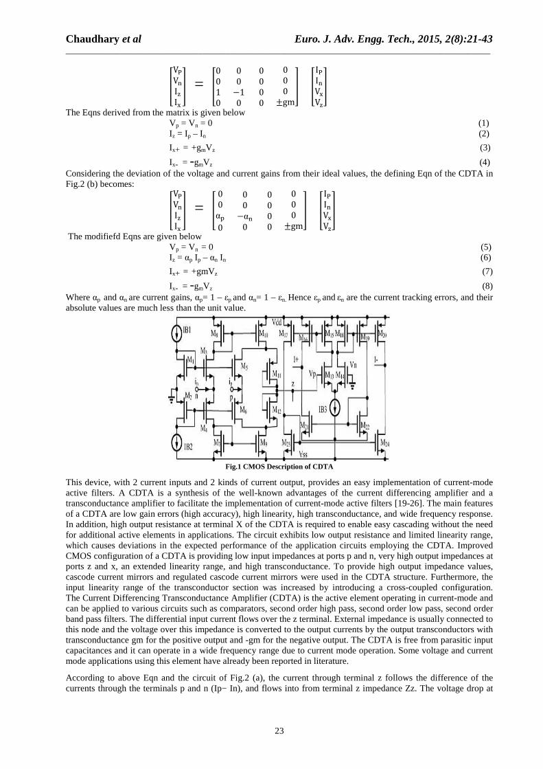
Integrator In integrator circuit the output voltage waveform is the integral of input voltage waveform it is known as integrator or integration amplifier. Such a circuit is designed using current differencing transconductance amplifier (CDTA).
Fig.11 Proposed circuit of Integrator using CDTA
In the designing of Integrator we use only a single CDTA and apply input at the positive terminal of CDTA and a feedback signal is feeded from the negative terminal of CDTA, with a capacitor and resistor. Transfer function of integrator using CDTA In a simple integrator Vi2 at negative terminal and Vi1 at positive terminal from the basic operation of CDTA Iout is the function of input voltages Iout = gm (Ii1 – Ii2) Due to this Iout Voltage across the capacitor. Transfer function of Integrator is
NOPQNR =
STJ) (24)
As we know that the cut-off frequency of the integrator is taken as
f0 = 1/2πR1C1 (25)
By putting the value of R1 C1 in Eqn 22, we can find out the frequency of the Integrator. Practical value of the integrator is 7.55 MHz Theoretical Value: f0 = 1/2πR1C1
R = 10 kΩ, C = 2 pf, f0 = 1/(2 x π x 10 x 103 x 2 x 10-12 )
f0 = 6.83 MHz The theoretical value is matched with the practical value. Simulation circuit of Integrator In the integrator circuit we are using a single CDTA with resistor and a capacitor. The CDTA is designed with the CMOS technology. In the integrator circuit we are applying input at the positive terminal and the feedback is feed from negative terminal of the CDTA And output is taken from the z terminal as shown in the Fig.11 the circuit is obtained by using a basic inverting configuration with a feedback resistor R and a capacitor C as per the desired output we can chose the value of R & C.
Chaudhary et al Euro. J. Adv. Engg. Tech., 2015, 2(8):21-43 _____________________________________________________________________________________________
33
Fig.11 Schematic diagram of integrator using CDTA
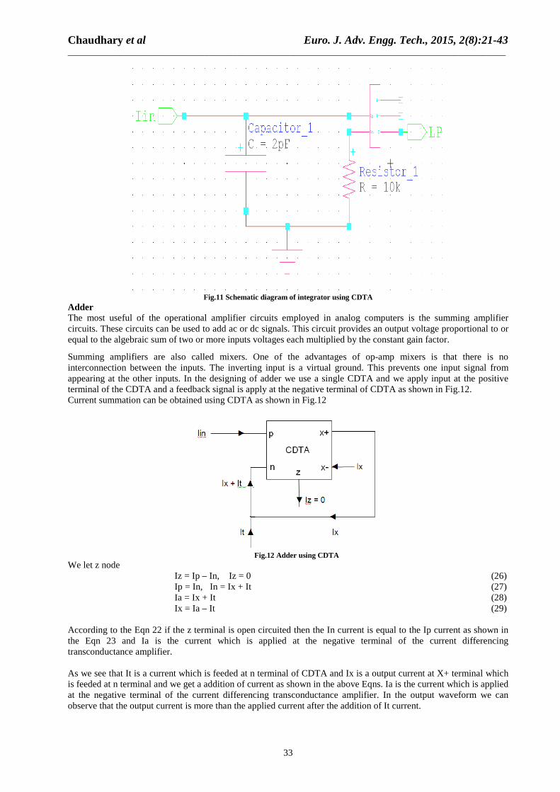
Adder The most useful of the operational amplifier circuits employed in analog computers is the summing amplifier circuits. These circuits can be used to add ac or dc signals. This circuit provides an output voltage proportional to or equal to the algebraic sum of two or more inputs voltages each multiplied by the constant gain factor.
Summing amplifiers are also called mixers. One of the advantages of op-amp mixers is that there is no interconnection between the inputs. The inverting input is a virtual ground. This prevents one input signal from appearing at the other inputs. In the designing of adder we use a single CDTA and we apply input at the positive terminal of the CDTA and a feedback signal is apply at the negative terminal of CDTA as shown in Fig.12. Current summation can be obtained using CDTA as shown in Fig.12
Fig.12 Adder using CDTA
We let z node Iz = Ip – In, Iz = 0 (26) Ip = In, In = Ix + It (27) Ia = Ix + It (28) Ix = Ia – It (29)
According to the Eqn 22 if the z terminal is open circuited then the In current is equal to the Ip current as shown in the Eqn 23 and Ia is the current which is applied at the negative terminal of the current differencing transconductance amplifier. As we see that It is a current which is feeded at n terminal of CDTA and Ix is a output current at X+ terminal which is feeded at n terminal and we get a addition of current as shown in the above Eqns. Ia is the current which is applied at the negative terminal of the current differencing transconductance amplifier. In the output waveform we can observe that the output current is more than the applied current after the addition of It current.

Chaudhary et al Euro. J. Adv. Engg. Tech., 2015, 2(8):21-43 _____________________________________________________________________________________________
34
Fig.13 Schematic diagram of Adder Using CDTA
Simulation Results of the Different Circuits
Fig.14 Frequency response of 2nd order low-pass BW filter
Fig.15 Frequency response of Integrator circuit
Chaudhary et al Euro. J. Adv. Engg. Tech., 2015, 2(8):21-43 _____________________________________________________________________________________________
35
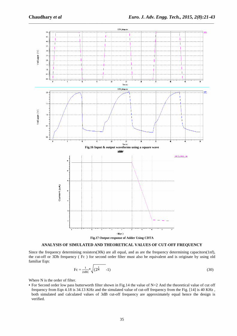
Fig.16 Input & output waveforms using a square wave
Fig.17 Output response of Adder Using CDTA
ANALYSIS OF SIMULATED AND THEORETICAL VALUES OF CUT -OFF FREQUENCY
Since the frequency determining resistors(30k) are all equal, and as are the frequency determining capacitors(1nf), the cut-off or 3Db frequency ( Fc ) for second order filter must also be equivalent and is originate by using old familiar Eqn:
Fc = &
π)*(24 -1) (30)
Where N is the order of filter. • For Second order low pass butterworth filter shown in Fig.14 the value of N=2 And the theoretical value of cut off
frequency from Eqn 4.18 is 34.13 KHz and the simulated value of cut-off frequency from the Fig. [14] is 40 KHz , both simulated and calculated values of 3dB cut-off frequency are approximately equal hence the design is verified.
Chaudhary et al Euro. J. Adv. Engg. Tech., 2015, 2(8):21-43 _____________________________________________________________________________________________
36
• When Iin = 0, the integrator works as a open loop amplifier. This is because the capacitor C acts as an open circuit (XC = infinite) to the input current. The input current charging capacitor C produce an error voltage at the output of integrator as shown in Fig.16, to reduce the error voltage at the output a resistor R is connected with the capacitor C. Thus R limit the low frequency gain and hence minimizes the variation in the output voltage the input signal integrated properly if the time period T of the signal is larger than or equal to RC. That is T ≥ RC.
• According to the Fig.17 the gain is reducing when we increase the frequency at the -3dB point the gain start decreasing at which the practical value of the frequency is 7.55 MHz and the theoretical which is derived from Eqn 3.13 value is 6.83 MHz both value are approximately same. Thus the design is verified.
• The circuit shown in the Fig.13 work as a current adder because we apply 50 µA and get 58 µA so it is clear from Eqn 3.14, 3.15, 3.16, 3.17 calculation that the circuit work as a adder.
UNIVERSAL FILTERS
A current-mode universal filter circuit is described. In this circuit we use single input and three outputs uses two CDTA only, one grounded capacitors. Since all capacitors are grounded, this is beneficial for integrated circuit. The circuit provides basic filtering functions such as lowpass, bandpass and highpass filters simultaneously from the same configuration. Tspice simulation results agree with the theoretical analysis. The passive and active sensitivities are low. The transconductance gain gm of the CDTA is directly proportional to the external bias current Ib which can be written as
gm = Ib/2VT (31) where VT = 26 mV at 27ºC is the thermal voltage.
A biquadratic filter is a very important filter for analog signal processing. There are many applications such as signal processing, TV receivers and wireless communications stages where narrow band pass tuned amplifiers are required such as in video signal applications. Using the second order ZC-CDTA filter structure shown in Fig.18 [3], the proposed circuits is composed of two ZC-CDTAs and two capacitors. The implementation of the circuit is realized without any resistors. Application circuits designed without resistance allow the design of integrated circuit structures occupying less area. The ZC-CDTA filter structure can be implemented at less area compared with 7 other filter applications designed with resistance. For example the second order filter structure given in includes four resistors and two capacitors. The production of the conventional filter structure is more expensive than the ZC-CDTA filter structure. The frequency response of the second order filter structure and the frequency response of the filter structure are shown in Fig.19 respectively. The ZC-CDTA filter structure is a developed version of the CDTA filter structure [7]. The conventional CDTA second order filter structure does not have high impedance high pass filter section. In this work, the fourth order filter is established by cascading second order low pass and high pass filters by the aid of Z copy. Note that the first filter section provides LP filter and the second section yields the HP function. Actually, the HP function is obtained as the current of C2. This current is reflected to the Z-Copy terminal where we obtain easily the BP function as the overall response. Also, note that this is not possible in filter structures employing conventional CDTAs without Z Copy terminal. The biquad filter, which has high quality factors can be designed by using ZCCDTA compared to CDTA filter structure.
FREQUENCY AGILE FILTER APPLICATION OF CDTA
Frequency, bandwidths, modulation can be controllable using computer tools in Software defined radio, or SDR. Reconfigurable receiver is possible to adapt to any frequency, band-width, modulation, etc., corresponding to the standards which were pre-selected. Cognitive radio which searches and uses a suitable band refers to wireless architectures in which a communication system does not operate in a fixed band. Cognitive radio is also built on the Software defined system. The software defined radio system is also applicable to provide a new solution for global positioning system to reply to the needs of five bands containing GPS, GLONASS, Galileo, Beidou, and GNSS. It is inevitable for the biggest possible versatility of future global navigation systems, including GPS, GLONASS, Beidou, GNSS and Galileo. Such architectures require reconfigurable analog elements: LNA, local oscillators, mixers and filters. The Z copied current differencing transconductance amplifier second order filter structure is modified with a feedback system to obtain reconfigurable filter structure.
This structure also called as frequency agile filter. The general second order filter structure which includes band-pass and low-pass output is given in Fig.18. The low-pass and band-pass filter output must be high impedance for current mode reconfigurable applications. The gain at f0 of the band pass output is GBP = 1 and -3 dB bandwidth is gm1 / 2πC1. The gain for the low pass output is gm1gm2. Fig.5.2 shows the second order current mode frequency agile filter general structure developed with second order filter structure. The output of the low pass section is applied to the input as feedback with a gain A obtained from electronically controllable second generation current conveyor.

Chaudhary et al Euro. J. Adv. Engg. Tech., 2015, 2(8):21-43 _____________________________________________________________________________________________
37
Proposed Model In this section design of Universal filter is proposed using CMOS based CDTA. Further frequency response of all three basic filter transfer functions are verified using TANNER TOOL. The signal flow graph for the proposed model is shown in Fig.19.
Fig.18 Model of CDTA based Universal filter
Fig.19 Signal flow graph of the proposed model
The transfer function of the above proposed filter is being derived as follows Transfer function of Low Pass filter
NVWN$% = ST&STST&ST, )3 ST&, ))3J3 (32)
Transfer function of Band Pass filter N(WN$% = )3ST&JST&ST, )3 ST&, ))3J3 (33)
Transfer function of High Pass filter NXWN$% = ))3J3ST&ST, )3 ST&, ))3J3 (34)
The pole angular frequency ωo and quality factor Q are given by:
ωY = ST&ST))3 (35)
Q = ST)ST&)3 (36)
Practical Value of Universal Filter: Cut-off frequency f0 = 2.30 GHz. Theoretical Value calculation for Universal Filter: As we know that the gain formula
gm1 = IB&µCox (37)
ω0 = ST&ST))3 (38) By using Eqns 5.7 & 5.8 we can find out the cut-off frequency of Universal filter as show below:
gm1= ST([\]J3), ST([\]J)
taking values from Tspice file
gm(NMOS_1) = 85x580x1x =.3a &bcd = 444.07x10Ke A/V
gm(NMOS_1) = 85x580x1x =.0a=.3a &bcd = 297.89 x 10Ke A/V
gm1= fff.bg &bch, ig.ji &bch = 370.98 x 10Ke

Chaudhary et al Euro. J. Adv. Engg. Tech., 2015, 2(8):21-43 _____________________________________________________________________________________________
38
gm2= ST(\]J3I, ST([\]Jk)
gm(PMOS_7) = 200 x 230 x 4 x ==.3a &bc3 = 1356.49 x 10Ke A/V
gm(NMOS_7) = 200 x 580 x 1 x a=.3a &bc3 = 1523.15 x 10Ke A/V
gm2 = (&noe.fi,&on) &bch = 1439.81 x 10Ke A/V
ωY = ST&ST))3 = &fni.j ngb.ij &bc3o &bcp & &bc3 = 1031.135 x 10g
f0 = &bn&.&no &bk = 164.044 x 10g = 1.64 GHz
Transconductance of CDTA for Universal filter is approximately choose as
gm = ST&,ST = 905.395 x 10Ke
Then the Frequency of Universal Filter is
ωY = ST&ST))3 = ibo.nio &bch b.o &bc3h = 2.03 GHz.
In this calculation our practical value is 2.30 GHz and our theoretical value is 2.03 GHz, which is shown in the output waveform Fig.19. Through this output frequency response we can compare the calculated value with the practical value and verify the design of universal filter which is designed with the help of current differencing transconductanse amplifier. In the circuit of universal filter we are using 2 CDTA Simulation Circuit of Universal Filter
Fig.20 Schematic diagram of Universal filter
LOW-PASS & BAND-PASS FILTERS
Analog filters are designed to process analog signals, while digital filters process analog signals using digital techniques [18]. Depending on the type of elements used in their construction, filters may be classified as active or passive. Elements used in passive low frequency operations, where LC filters are used for RF or high frequency operation. filters are resistors, capacitors and inductors. And elements used in the active filters are transistors operational amplifiers in addition to resistors and capacitors. The type of elements used to dictate the operating frequency range of the filter. Example, RC filters are commonly used for audio. The response of a practical low-pass filter is divided into two bands a pass-band and stop-band. For certain filters, gain varies up and down (ripples) in the pass-band in the stop-band or in both. How rapidly the gain falls off as the stop-band is entered is known as the roll-off. The roll-off increased by 20 db/decade with each increase in order of the filter [22]. As we know that the order of the filter is equal to the number of resistor-capacitor pair in the circuit. So increasing the circuit complexity by adding an R-C pair increases the circuit’s order and also increases the roll-

Chaudhary et al Euro. J. Adv. Engg. Tech., 2015, 2(8):21-43 _____________________________________________________________________________________________
39
off rate by 20 db/decade. The roll off rate may be specified in db/decade. A decade increase in frequency means that the frequency increased 10 times.
Gain = !"# $% (39)
Low-Pass filter is a filter which passes the low frequency signal and blocks the high frequency signal. A low-Pass filter has a constant gain from 0 Hz to a cutoff frequency fc. Therefore the bandwidth is also fc. At fc the gain is down by 3 db, after that (f > fc) it decreases with the increase in input frequency. The frequency between 0 Hz to fc are known as the pass-band frequencies as shown in the Fig.21. A band-pass filter is a circuit which is designed to pass signals to only in a certain band of frequencies while attenuating all signals outside the band. The main parameters in a band-pass filter are the high and low cutoff frequencies (f1 and fh), the bandwidth (BW) the centre frequency fC.
Δf = (fh – f1) (40) fC = √f1rh (41)
On a log plot, fC is a halfway between fh and f1. This is not true on a linear plot. The selectivity, Q is defined Δf.centre as the ration of bandwidth frequency fC and
Q = tu (42)
Fig.21 (a) Low-Pass Filter response (b) Band-Pass Filter Response
Band-Pass filter is a filter which have a pass-band between two cutoff frequenciesf1 and fh where fh > f1, and two stop bands 0 < f < f1 and f > fh. A Band-Pass filter has a zero gain from 0 Hz to f1 and f > fh, as shown in Fig.21 (b). The current transfer function for Low-pass and Band-pass responses is given as
vVWv$% = wxx3y3z yx z wxx3 (43)
v(Wv$% = yxy3z yx z wxx3 (44)
The filter performance factors ωo, ωo/Q and Q are given as
ωo = S))3 (45)
!| = x (46)
Q = wx3) (47)
From Eqns 4.15 and 4.16, it is clear that ωo can be electronically tuned by g independently of !| and Q can be tuned by C2.
Simulation circuit of Low-pass and Band-pass filter This section includes the responses obtained by the schematic level simulations. The schematic drawn in S-Edit unit of Tanner EDA Tool and the simulations are completed in T-Spice unit of Tanner EDA Tool. As shown in Fig.21.

Chaudhary et al Euro. J. Adv. Engg. Tech., 2015, 2(8):21-43 _____________________________________________________________________________________________
40
Fig.22 Schematic diagram of LP, BP filter using CDTA
Simulation Results of Universal Filters
Fig.23 Output response of the Universal filter
Fig.24 Output response of LP, BP filter

Chaudhary et al Euro. J. Adv. Engg. Tech., 2015, 2(8):21-43 _____________________________________________________________________________________________
41
Analysis of simulated Results • Universal filter shown in Fig.23. Theoretical value of the cut-off frequency from Eqn 4.8 is 2.03 GHz after
calculation and the simulated value of cut-off frequency is 2.30 GHz , both simulated and calculated values of 3dB cut-off frequency are approximately equal hence the designed is verified.
• A proposed model is simulated using TANNER TOOL 13.0. A CDTA was realized by the CMOS technology. The supply voltage were taken Vdd=2.5 V, C1= 1.8pF, C2=3pF realize a frequency response is 937.95 MHz. The simulated magnitude response of low-pass, band-pass taken from the different output terminals are shown in the Fig.24 respectively.
CONCLUSION
In communication systems filters use as an integral part of overall system. According to specifications and the application filters are designed using various ways, Butterworth filter, known for its good transient response and maximally flat pass band is used widely in communication systems data and video transmission. The design procedure is developed for Active-RC Butterworth filter. For this first a selection is made for the active device used. CDTA is selected and a design procedure to design the CDTA is defined. The frequency response is simulated using the T-Spice environment of Tanner EDA tool. The simulated results of the CDTA are in compliance with the theoretical values. The development of a design procedure provides a quick, well-integrated and effective mechanism for estimating the filter parameters. The steps highlighted make it easy to redesign the circuit for different sets of specifications. The design procedure is developed keeping in view few approximations that are made on the basis of basic know-how of the filter responses and the effect of the active device on the frequency response estimated by RC network. The results of SPICE simulation for the versatile Quadrature Oscillator are shown in agreement with the results calculated by use of design Eqns and methodology. Versatile Quadrature Oscillator are designed, has generates frequency of 2.5 MHz, DC Gain of unity. So, these filter specifications are quite favorable with that of the video frequency. Further, Active-RC filters of different orders are designed. The analysis is done to show the change in filter pass-band frequency with increase in order. This analysis validates the results of the filter design. The proposed Universal Filter circuit uses two Cascode CMOS based CDTAs, two capacitors. The main reason for employing Universal filter using Cascode CMOS based CDTA is due to its less complex structure which consumes less amount of area consumes less power and provides high speed of operation. Simulation results verified that Universal filter designing using CMOS based CDTA provides high amount of controllability of circuit parameters as compared to current conveyor and op-amp based Universal filter. Oscillation condition and oscillation frequency can be adjusted independently with the input bias currents. It can provide quadrature sinusoidal signals in both voltage-mode and current-mode simultaneously. This is one method to design a Universal filter and Active-RC Butterworth filter using CDTA. Other active devices like DDA and second generation current- controlled conveyors (CCCII) can also be used. The design can be developed keeping in view low power and low voltages constraints as the filters are now being used in many portable applications that have requirement of low power and low voltages. Methods can be developed to reduce the steep increase in power dissipation and component count with increase in the filter order. Active devices can be designed in such a way that they may not restrict the pass-band frequency from expected pass-band frequency.
REFERENCES [1] AT Bekri and F Anday, Nth-Order Low-Pass Filter Employing Current Differencing Transconductance Amplifiers, Proceeding of the European Conference on Circuit Theory and Design, Cork, 2005, 193-196. [2] A Uygur and H Kuntman, Design of a Current Differencing Transconductance Amplifier (CDTA) and It’s Application on Active Filters, SIU2005: IEEE 13th Signal Processing and Communication Applications Conference, Kayseri, 2005, 340-343. [3] Anisur R Nasir and SN Ahmad, Current-Mode Single-Input Multi-Outputs Universal Filter Employing CDTAs, International Journal of Electronics & Communication Technology, IJECT Vol. 3, Issue 2, April - June 2012 ISSN : 2230-7109 (Online) | ISSN : 2230-9543 (Print ) [4] Adel S Sedra and Kenneth C Smith, Microelectronics Circuits, Oxford University Press, Fifth Edition, 2004. [5] SPR Almazan and MTG de Leon, A 3rd Order Butterworth Gm-C Filter for WiMAX Receivers in a 90nm CMOS Process, 12th International Conference on Computer Modelling and Simulation (UK Sim), 2010, 625-630. [6] E Armağan and H Kuntman, Design of Balanced Differential Pair Based CCCII Circuit and ConFigureurable Frequency Agile Filter Application in 28nm Process, Conference on Electrical and Electronics Engineering Bursa, Turkey, 2012, 257 - 261. [7] E Armagan and H Kuntman, ConFigureurable Frequency Agile Filter Application of Balanced Differential Pair Based CCCII Circuit in 28nm Process, 4th IEEE Latin American Symposium on Circuits and Systems, Cusco, Peru, 2013, 1 - 4.

Chaudhary et al Euro. J. Adv. Engg. Tech., 2015, 2(8):21-43 _____________________________________________________________________________________________
42
[8] R Arslanalp, AT Tola and SS Yilmaz, High Frequency Log Domain All Pass Filter based on KHN Topology, 15th IEEE International Conference on Electronics, Circuits and Systems (ICECS), 2008, 129-132. [9] D Baez-Lopez, G Espinosa, LIV Jurez and FM Hernandez, A Scheme for the KHN State Variable Filter to Improve its High Frequency Performance, Midwest Symposium on Circuits and Systems, 1998, 444-447. [10] D Baez-Lopez, C Cabrera-Oerez, S Bautista-Cadena and JM Ramirez, A Modified Fully Biquadratic State-Variable KHN Filter Using only 3 Op-Amps, Canadian Conference on Electrical and Computer Engineering,1994, 543-544. [11] Razavi Behzad, Design of Analog CMOS Integrated Circuits, Tata McGraw- Hill Publishing Company Limited, Edition 2002. [12] D Biolek, CDTA-Building Block for Current-Mode Analog Signal Processing, European Conference on Circuit Theory and Design, Cracow, Poland, 2003, 397 - 400. [13] L Bouzerara and MT Belaroussi, Low Voltage, Low Power and High Gain CMOS Operational Tansconductance Amplifier, IEEE International Symp. on Circuits and Systems, 2002, 1, 1325-1328. [14] C Acar and S Õzoguz, A New Versatile Building Block: Current Differencing Buffered Amplifier, Microelectronics Journal, 1999, 30, 157-160. [15] Cheng-Chung Hsu, Wu-Shiung Feng, Testable Design of Multiple-Stage OTA-C Filters, IEEE Transactions on Instrumentation and Measurement, 2000, 49 (5), 929-934. [16] Chunlei Shi, Yue Wu, Hassan O Elwan and Mohammed Ismail, A Low-Power High - Linearity CMOS Baseband Filter for Wideband CDMA Applications, IEEE International Symposium on Circuits and Systems, Switzerland, 2000. [17] D Biolek and V Biolkova, CDTA-C Current-Mode Universal 2nd Order Filter, Proceeding of the 5th WSEAS International Conference on Applied Informatics and Communications, Malta, 2005, 411-414. [18] H Daoud, H, S Ben Salem, S Zouari M Loulou, Folded Cascade OTA Design for Wide Band Applications, International Conference on Design and Test of Integrated Systems in Nanoscale Technology, 2006, 437-440. [19] Darwin Cheung, Klaas Bulty and Aaron Buchwaldy, 10-MHz 60-dB Dynamic Range 4th Order Butterworth Low pass Filter, IEEE press, 1997, 248-251. [20] Dinesh Prasad, DR Bhaskar and AK Singh, Universal Current-Mode Biquad Filter using Dual Output Current Differencing Transconductance Amplifier, International Journals of Electronics and Communication, 2009, 63, 497-501. [21] RE El-Queseny, Soliman A Mahmoud and MM Ibrahim, Modelling of Active Compensated KHN Band Pass Filter using Standard Hardware Description Language, International Conference on Microelectronics (ICM), 2009, 70-73. [22] Rajni, Design of High Gain Folded-Cascode Operational Amplifier Using 1.25 um CMOS Technology, International Journal of Scientific & Engineering Research Volume 2, Issue 11, November-2011 ISSN 2229-5518 [23] Ersin Alaybeyoğlu, Hulusi Hakan Kuntman, SY Sun, A New CMOS ZC-CDTA Realization and its Filter Applications, IEEE Eurocon 2013 [24] Firat Kacar, Hulusi Hkan Kuntman, A New Improved CMOS Realization of CDTA and its Filter Applications, Turk J Elec Eng & Comp Sci, Vol.19, No.4, 2011, c TUB¨ ˙ ITAK doi:10.3906/elk-1003-467 [25] Franco Maloberti, Analog Design for CMOS VLSI Systems, Kluwer Academic Publisher, Boston, Dordrecht, London, 2001. [26] A Gerosa, A Ready-to-Use Design Procedure for Operational Transconductance Amplifiers that Minimizes Power Consumption, 8th IEEE International Conference on Electronics, Circuits and Systems, 2001, 949-952. [27] S Haykin, Cognitive Radio: Brain-Empowered Wireless Communications, IEEE Journal on Selected Areas in Communications, 2005, 23, 201 - 220. [28] MA Ibrahim and H Kuntman, A New VM KHN-Filter Suitable for MOSFET-C Technology, Proceedings of the 12th IEEE Conference on Signal Processing and Communications Applications, 2004, 125-128. [29] John G Proakis and Dimtris G Manolakis, Digital Signal Processing: Principles and Algorithms and Applications, Third Edition, 2001. [30] Jie Jin and Chunhua Wang, Current-Mode Universal Tier and Quadrature Oscillator using CDTAS, Turk Journal of Electrical Engineering & Computer Science, 2014, 22, 276-286. [31] MF Abate, A Mixed Signal Tester Standard Tracable AC Calibration of Analog Modules, Proceeding of VLSI Test Seep, New Jersey, 1992, 85–89. [32] M Sagbas and K Fidanboylu, Electronically Tuneable Current-Mode Second-Order Universal Filter using Minimum Elements, Electronics Letters, 2004, 40, 2-4. [33] C Muniz-Montero, A Diaz-Sanchez, and R Gonzalez-Carvajal, A Very Compact KHN Filter with Multidecade Tuning, 18th European Conference on Circuit Theory and Design, 2007, 44-47. [34] C Muniz-Montero, R Gonzalez-Carvajal, A Diaz-Sanchez and JM Rocha, Low Frequency, Current Mode Programmable KHN Filters using Large-Valued Active Resistors, IEEE International Symposium on Circuits and Systems, 2007, 3868-3871.

Chaudhary et al Euro. J. Adv. Engg. Tech., 2015, 2(8):21-43 _____________________________________________________________________________________________
43
[35] S Olmez and U Cam, A Novel Square Root Domain Lossless Integrator and its Application to KHN Biquad Filter Design, International Conference on Electrical and Electronics Engineering (ELECO), 2009, 227-231. [36] FCW Po, Leti Minatec, E DeFoucauld, D Morche and P Vincent, A Power Optimized Transconductance Amplifier and its Application to a 6th Order Low-Pass GMC Filter, 16th IEEE International Conference on Electronics Circuits and Systems, 2009, 631-634. [37] RL Geiger and E Sanchez-Sinencio, Active Filter Design Using Operational Transconductance Amplifiers: A Tutorial, IEEE Circuits and Devices Magazine, 1985, 1. [38] RG Eschuzier, LPT Kerklaan and JH Huising, A 100 MHz 100dB Operational Amplifier with Multipath Nested Miller Compensation, IEEE Journal of Solid State Circuits, 1992, 27, 1709-1717. [39] Raghuwar Sharan Gautam, PK Jain and DS Ajnar, Design of Low Voltage Folded Cascode Operational Transconductance Amplifier with Optimum Range of Gain and GBW in 0.18μm Technology, International Journal of Engineering Research and Applications(IJERA), 2012, 2(1), 566-570. [40] Randall L Geiger and Edgar Sánchez-Sinencio, Active Filter Design Using Operational Transconductance Amplifiers: A Tutorial, IEEE Circuits and Devices Magazine, 1985, 1, 20-32. [41] Roewer and Kleine, A Novel Class of Complementary Folded Cascade OP Amps for Low Voltage, IEEE Journal of Solid- State Circuits, 2002, 37 (8), 1080–1086. [42] Roman Sotner, Zden_ek Hrubos, Bretislav Sevcik, Josef Slezak, Jiri Petrzela and Tomas Dostal, An Example of Easy Synthesis of Active Filter and Oscillator using Signal Flow Graph Modification and Controllable Current Conveyors, Journal of Electrical Engineering, 2011, 62 (5), 258–266. [43] SC Dutta Roy, On Maximally Flat Sharp Cutoff Low-Pass Filters, IEEE Trans. Audio Electroacomst. 1971, AU-19, 58-63. [44] M Uddin Shaber and S Signell, Fully Differential Gain-Boosted OTA Design for Pipeline DA-Converter in 180nm CMOS Technology, 12th IEEE International Conference on Electronics, Circuits and Systems, 2005, 1-4. [45] Wang Chunhua, Zou Deshu, Yan Jianzhuo, Shi Chen, A MOCCII Current-Mode KHN Filter and its Non-Ideal Characteristic Research, 4th International Conference on ASIC, 2001, 289- 292. [46] William L Brown and Andrew YJ Szeto, Reconciling Spice Results and Hand Calculations: Unexpected problems, IEEE Transaction on Education, 2000, 43(1):43-51. [47] X Zheng, BJ Maundy, EI El-Masry and IG Finvers, A Novel Low-Voltage Operational Transconductance Amplifier and its Applications, IEEE Int. Symp. Cir. System, Geneva, 2000. [48] M Yavari and O Shoaei, Low-Voltage Low-Power Fast-Settling CMOS Operational Transconductance Amplifiers for Switched-Capacitor Applications, IEEE Proceedings on Circuits, Devices and Systems, 2004, 151 (6), 573-578. [49] S Yamacli, S Ozcan and H Kuntman, Resistorless Tuneable KHN-Filter in Current Mode with CCCIIs and Grounded Capacitors, 15th IEEE International Conference on Electronics, Circuits and Systems, 2008, 324-327.