design of digital circuits (s4) - tu clausthaltech · design of digital circuits (s4) chapter 2,...
TRANSCRIPT

Design of Digital Circuits (S4)
Chapter 2, Part 1
Synthesis and logic optimizationSection 2.1 Register transfer synthesis
to 2.3 Binary decision diagram
Prof. G. Kemnitz
Institute of Informatics, Technical University of ClausthalMay 14, 2012
Prof. G. Kemnitz · Institute of Informatics, Technical University of Clausthal May 14, 2012 1/135

RT synthesis1.1 Register1.2 Combinational circuits1.3 Processing + sampling1.4 Latches1.5 Constraints1.6 Entwurfsfehler1.7 Zusammenfassungf1.8 Aufgaben
Logikoptimierung2.1 Umformungsregeln2.2 Optimierungsziele2.3 Konjunktionsmengen
Prof. G. Kemnitz · Institute of Informatics, Technical University of Clausthal May 14, 2012 1/135

2.4 KV-Diagramme2.5 Quine und McCluskey2.6 Aufgaben
BDD3.1 Vereinfachungsregeln3.2 Operationen mit ROBDDs3.3 ROBDD ⇒ minimierte Schaltung3.4 Aufgaben
Prof. G. Kemnitz · Institute of Informatics, Technical University of Clausthal May 14, 2012 2/135

Synthesis
Search for circuit with the same function. Problem timing:
can be solved only for run time tolerant circuits(optimization, technology mapping etc. change timing)no pre-specified delay ⇒ simulation model without delaysame function ⇒ same output values when the outputsignals are valid
compare window
v0 v1
w0 w1
clock
simulation output withwith hold and delay times
simulation outputsyntheses description
Prof. G. Kemnitz · Institute of Informatics, Technical University of Clausthal May 14, 2012 2/135

Synthesis descriptions are simplified simulation models:
without delay times (no after statements, no waitstatements etc.)without check of validity and other plausibility tests (nooutput of text messages, no pseudo value for �invalid etc.).
After resolving hierarchy it consists of:
pre-designed circuits, which synthesis transfers unchangedcombinatorial processes with undelayed signal assignmentsandsampling processes with undelayed signal assignments andwithout check of setup and input hold conditions.
Prof. G. Kemnitz · Institute of Informatics, Technical University of Clausthal May 14, 2012 3/135

1. RT synthesis
RT synthesis
Prof. G. Kemnitz · Institute of Informatics, Technical University of Clausthal May 14, 2012 4/135
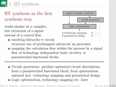
1. RT synthesis
RT synthesis as the firstsynthesis step
register transfer synthesis
logic optimization
circuit generator
geometrical designtechnology mapping
works similar as a compiler,but extraction of a signalinstead of a control flow
resolving hierarchy⇒ circuitstructure out of predesigned subcircuit an processesmapping the calculation flow within the process by a signalflow of technology independent basic circuitry orparametrized functional blocks
Circuit generators: produce optimized circuit descriptionsfrom a parametrized functional block; local optimization,optional incl. technology mapping and geometrical design.Logic optimization, technology mapping etc. later
Prof. G. Kemnitz · Institute of Informatics, Technical University of Clausthal May 14, 2012 5/135

1. RT synthesis
Mapping control flow ⇒ signal graph
is already without timing an ill posed problem:
for most imperative functional descriptions no circuit existswith the same functionmultiple ways to describe the same circuitsmall changes in description allows new completely differentinterpretations
Twist the objective:
How the description must look, so that the synthesis createsa correct circuit?
How registers, combinatorial circuits, etc. have to be described,so that the synthesis recognize them.
Prof. G. Kemnitz · Institute of Informatics, Technical University of Clausthal May 14, 2012 6/135
1. RT synthesis 1. Register
Register
Prof. G. Kemnitz · Institute of Informatics, Technical University of Clausthal May 14, 2012 7/135

1. RT synthesis 1. Register
Description and extraction of registers
Simulation model (all ready simplified):
process(T)beginif RISING EDGE(T) thenif x’LAST EVENT>ts then --- check setup condition
y <= invalid after thr, x after tdr;
elsey <= invalid after thr;
end if;end if;
end process;
further simplifications for synthesis:
no means to describe timing, validity, ...no check of setup and input hold conditionsno text output (warnings, error messages).
Prof. G. Kemnitz · Institute of Informatics, Technical University of Clausthal May 14, 2012 8/135

1. RT synthesis 1. Register
--- Register template with initialisation
process(I, T)beginif I=’1’ then--- or if I=’0’ then
y <= initialization value;elsif RISING EDGE(T) then--- or elsif FALLING EDGE(T) then
y <= x;end if;
end process;
--- without initialisation
process(T)beginif RISING EDGE(T) then--- orr elsif FALLING EDGE(T) then
y <= x;end if;
end process;
T/Tactive clock edge
rising edgefalling edge
x y
table datatype (bit,bitvector, number, ...)
tTyptTyp
tTyp
xI
T/Tactive clock edge
initialization signal
yx
rising edgefalling edge
low aktivehigh active
I/I/0
tTyp tTyp
in binary signals conver-
Prof. G. Kemnitz · Institute of Informatics, Technical University of Clausthal May 14, 2012 9/135

1. RT synthesis 1. Register
Sample process ⇔ register
given are three sampling processes
signal a,b,c,d: STD LOGIC;
signal K,L,M: STD LOGIC VECTOR(2 downto 0);
no initialization; sampling withthe rising edge of a
process(a)beginif RISING EDGE(a) thenK(0) <= d;K(1) <= K(0);K(2) <= K(1);
end if;end process;
Initialization with c = 1; samplingwith the falling edge of b
process(b, c)beginif c=’1’ thenL <= ”000”;
elsif FALLING EDGE(b)thenL <= K;
end if;end process;
Prof. G. Kemnitz · Institute of Informatics, Technical University of Clausthal May 14, 2012 10/135

1. RT synthesis 1. Register
Initialization with c = 1; samplingwith the raining edge of a
process(a, c)beginif c=’1’ then
M <= ”010”;elsif RISING EDGE(a)thenM <= K;
end if;end process;
inputs, outputs and parameters of the described registers
data input signal d K(0) K(1) K K
data output signal K(0) K(1) K(2) L M
bit width 1 1 1 3 3
clock signal a ↑ a ↑ a ↑ b ↓ a ↑
initialization signal – – – c (H) c (L)
initialization value – – – 000 010
↑ – rising edge; ↓ – falling edge; H – high active; L – low activeProf. G. Kemnitz · Institute of Informatics, Technical University of Clausthal May 14, 2012 11/135

1. RT synthesis 1. Register
Register transfer synthesis
extraction of the terminals and parameters of all describedregistersForwarding the data to circuit generators; generation of theregisters
The designer
must stick to the description templatesmay summarize all registers withe the same initializationand sampling conditions in one sampling process
Advantage of less processes
less calculation effort for simulationless time critical transitions between different clocked circuitparts
Prof. G. Kemnitz · Institute of Informatics, Technical University of Clausthal May 14, 2012 12/135

1. RT synthesis 2. Combinational circuits
Combinational circuits
Prof. G. Kemnitz · Institute of Informatics, Technical University of Clausthal May 14, 2012 13/135

1. RT synthesis 2. Combinational circuits
Synthesis description of a combinational circuits
imperative behavioral model of a combinatorial circuit:
if one of the input signal switches, new calculation of theoutput; no memory
Description template:
process with all input signals in the sensitivity liststore interim results in the calculation in variables (notsignals!)no further processing of interim results from previouswake-up datesin each path of control a value must be assigned to eachoutput signal.
additional simplifications for synthesis: no delay, no check forvalidity
Prof. G. Kemnitz · Institute of Informatics, Technical University of Clausthal May 14, 2012 14/135

1. RT synthesis 2. Combinational circuits
If synthesis finds a process which complies with all rules:
extract of the control flow
substitute operators by logic gates
produce case distinctions by multiplexers.
Prof. G. Kemnitz · Institute of Informatics, Technical University of Clausthal May 14, 2012 15/135

1. RT synthesis 2. Combinational circuits
Circuits of basic gates
ba
&
ba ≥1
ba ≥1
y
y <= a or b
y <= a nor b
y
ba
=1
ba
=1
a
01
b
ay
s
ba
& y
y <= a and b
y
y <= a nand b
signal a, b, s, y: tBit ;
y
y
y <= a xor b
y <= a xnor b
y <= not aif s=1 theny<= a;
else y<= b;end if ;
(tBit: BIT, BOOLEAN or STD LOGIC; BOOLEAN: TRUE 7→ 1, FALSE 7→0; using STD LOGIC the pseudo values for �invalid� etc. remainsunused)
Prof. G. Kemnitz · Institute of Informatics, Technical University of Clausthal May 14, 2012 16/135

1. RT synthesis 2. Combinational circuits
Description & extraction of gates
signal x: STD LOGIC VECTOR(4 downto 0);
signal y: STD LOGIC VECTOR(1 downto 0);
...process(x)variable v: STD LOGIC VECTOR(1 downto 0);
beginA1: v(0):= x(0) and x(1);A2: v(1):= v(0) nor x(3);
A3: y(0)<=(v(0) andx(2)) or v(1);
A4: y(1)<=((not x(4))
or x(3)) nand v(1);
end process;
x2
x1
x0
y1
y0
v0
v1x3
x4
&&
≥1&
≥1
A1
A2
A3
≥1
A4
Prof. G. Kemnitz · Institute of Informatics, Technical University of Clausthal May 14, 2012 17/135

1. RT synthesis 2. Combinational circuits
From case distinctions to multiplexers
if control flow branches by �If� or �Case� instructionsoutput or interim values has to be assign in each branchIf-Elsif becomes a multiplexer chain
signal a, b, c, p, q, y: STD LOGIC;
...process(a, b, c, p, q)beginif p=’1’ then y<=a;elsif q=’1’ then y<=b;else y<=c;end if;
end process;
01 0
1a
b
c
pq
y
instead of �Else� it is also possible to overwrite a defaultvalue (even for signals):
y<=c;if p=’1’ then y<=a; end if;
Prof. G. Kemnitz · Institute of Informatics, Technical University of Clausthal May 14, 2012 18/135

1. RT synthesis 2. Combinational circuits
Parametrized functional blocks
operators with bit vector operands⇒ functional blocks with bit sizes as parametersarithmetic operation and compare (>, ≥ etc.)⇒ additional parameter: number representationselect statements with more than two cases⇒ additional parameters: selection values for each datainput
register transfer synthesis:
extraction of functional blocks and its parameters
circuit generators:
building the circuits out of basic gates; optional incl.technology mapping, ...
Prof. G. Kemnitz · Institute of Informatics, Technical University of Clausthal May 14, 2012 19/135

1. RT synthesis 2. Combinational circuits
Select statement ⇒ parametrized multiplexer
signal s: STD LOGIC VECTOR(1 downto 0);
signal x1,x2,x3,x4, y: STD LOGIC VECTOR(3 downto 0);
...
process(s, x1, x2, x3,x4)
begincase s iswhen ”00” => y <= x1;when ”01” => y <= x2;when ”10” => y <= x3;when others => y <= x4;
end case;end process;
00
01
11
10y
x1
x2
x3
x4
s2
4
4
4
4
4
parameters: data bit size and select valueslast selection value must be �others�1
1On one hand selection values such as �0X�, �XU� are forbidden insynthesis descriptions, on the other hand a case-statement has to take intoaccount the whole range of selection values.
Prof. G. Kemnitz · Institute of Informatics, Technical University of Clausthal May 14, 2012 20/135

1. RT synthesis 2. Combinational circuits
Bit comparators
x0 = 0x0x1 x0 6= 0 x0 = 1 x0 6= 1 x1 = x0 x1 6= x0
x0
x1=1
x0
x1==x0 x0x0 x0
01 FALSE TRUE(0) (1)0 1 FALSE TRUE TRUE FALSE FALSE TRUE(0) (1) (1) (0) (0) (1)
1 1 TRUE FALSE(1) (0)
00 TRUE FALSE FALSE TRUE TRUE FALSE(1) (0) (0) (1) (1) (0)
branch values in if-statements are generally produced bycomparisonsin synthesis the Boolean values �false� and �true� aremapped to the value range {0, 1}
Prof. G. Kemnitz · Institute of Informatics, Technical University of Clausthal May 14, 2012 21/135

1. RT synthesis 2. Combinational circuits
Arithmetical operations (+, −, *) and >, ≥ etc.
only defined for number and bit vector types
the circuit to be generated depends on the numberrepresentation (natural, whole numbers, floating point, ...)
types of bit vectors for number representation in this lecture:
--- for unsignd whole numbers
tUnsigned is array (NATURAL range <>) of STD LOGIC;
--- for signd whole numbers
tSigned is array (NATURAL range <>) of STD LOGIC;
defined together with the arithmetical, logical and compareoperations in the package �Tuc.Numeric Synth�
Prof. G. Kemnitz · Institute of Informatics, Technical University of Clausthal May 14, 2012 22/135

1. RT synthesis 2. Combinational circuits
Data flow symbols for compare operators
n
n
n
n
n
n
n
n
n
n
n
n
0 elseb
a
0 elseb
a
0 elseb
a
0 elseb
a
0 elseb
a
/=
<
<=
>
>=
1 if a = b0 else
==b
a
1 a 6= b
1 if a < b
1 if a ≤ b
1 if a > b
1 if a ≥ b
signal a, b: t[Un]signed(n-1 downto 0);
parameters:
bit size n
data type (signed or unsigned whole numbers) 2
2Other number types will not be used for synthesis in this lecture.
Prof. G. Kemnitz · Institute of Informatics, Technical University of Clausthal May 14, 2012 23/135

1. RT synthesis 2. Combinational circuits
Addition, subtraction and multiplication
signal a: T[Un]signed(n-1 downto 0);
signal b: T[Un]signed(m-1 downto 0);
constant c: T[Un]signed(m-1 downto 0);
a−ca+c
a+b a−b
max(n,m)n−c
n
m
n
n+c
max(n,m)
max(n,m)
m
n
∗ c
m
n
*
n+m
n+ma*b
a*c
max(n,m)a−b
a a
abb
a
a
+ba
ba
subtractor multiplieradder
sum and difference have the bit size of the larges operandthe bit size of a product is the sum of the bit sizes of theoperandsoperations not listed here (division, power) are generallyrealized by an operation sequence
Prof. G. Kemnitz · Institute of Informatics, Technical University of Clausthal May 14, 2012 24/135
1. RT synthesis 2. Combinational circuits
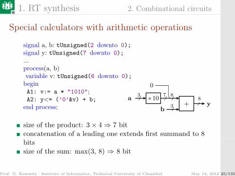
Special calculators with arithmetic operations
signal a, b: tUnsigned(2 downto 0);
signal y: tUnsigned(7 downto 0);
...process(a, b)variable v: tUnsigned(6 downto 0);
beginA1: v:= a * "1010";A2: y<= (’0’&v) + b;
end process;
a
0
+8
y
7
3
83
b
∗ 10
size of the product: 3× 4⇒ 7 bitconcatenation of a leading one extends first summand to 8bitssize of the sum: max(3, 8) ⇒ 8 bit
Prof. G. Kemnitz · Institute of Informatics, Technical University of Clausthal May 14, 2012 25/135

1. RT synthesis 2. Combinational circuits
Circuit with adder, comparator, multiplexer andgates
signal a, b, y: tUnsigned(3 downto 0);
signal e, f: STD LOGIC;
...process(a, b, e, f)beginif (a>"0011") and (e or f) =’1’ theny <= a+b;
elsey <= b;
end if;end process;
4
4
44+
a
b
≥1
>&
ef
0011
y10
Prof. G. Kemnitz · Institute of Informatics, Technical University of Clausthal May 14, 2012 26/135

1. RT synthesis 2. Combinational circuits
One select statement, multiple multiplexers
w2w1t1 t2
t1
t1
t1
w2w1 =>=>=>
casewhenwhenwhen
end case;
s is
w3w4
t2
t2
t2w3
else
w4
w3
else
{w1,w2,w3, ...}s
usonst
t1, t2 – any bit or bitvector type
u := a;u := b;
Mux1
v := c;v := d;
Mux2
u :=uelse;
a
b d
c
vu
vsonst
v :=velse;
assignment of a default value before the select statementoverwrite the default value for select values assigning adifferent value
Prof. G. Kemnitz · Institute of Informatics, Technical University of Clausthal May 14, 2012 27/135

1. RT synthesis 2. Combinational circuits
Describing a truth table by a case statement
signal x: STD LOGIC VECTOR(3 downto 0);
signal y: STD LOGIC;
...
process(x)begincase x iswhen "1000"|"0100"|"0010"|"0001"
=> y <= ’1’;
when others => y <= ’0’;
end case;end process;
x0x1x2x3 y
00
0
000
01
11
1 0
00 0
0
11110else
Prof. G. Kemnitz · Institute of Informatics, Technical University of Clausthal May 14, 2012 28/135

1. RT synthesis 3. Processing + sampling
Processing + sampling
Prof. G. Kemnitz · Institute of Informatics, Technical University of Clausthal May 14, 2012 29/135

1. RT synthesis 3. Processing + sampling
Combinatorial circuit and sampling register
Combining combinatorial circuitry with the subsequent registerin a sampling process reduces simulation effort; changes indescription starting from a pure combinatorial process:
clock instead all input signal in the sensitivity listaligning signal assignments to the active clock edgeoptional initialization (in addition initialization signal in thesensitivity list etc.)
process(I, T)
if I=active theny <= initial value;
elsif active clock edge of T thenoutput calculation of the processing function;
y <= assigning the processing result;
end if;
end process;
Prof. G. Kemnitz · Institute of Informatics, Technical University of Clausthal May 14, 2012 30/135

1. RT synthesis 3. Processing + sampling
Combinatorial circuit with output register
signal a, b, y: STD LOGIC VECTOR(4 downto 0);
signal T, e, f: STD LOGIC;
...process(T)beginif RISING EDGE(T) then
if (a>"0011") and(e or f) =’1’ then
y<= a+b;
elsey<=b;
end if;end if;
end process;
4
4
44 4+
a
b
≥1
>&
ef
0011T
combinatorialcircuit
samplingregister
y
1
0
Prof. G. Kemnitz · Institute of Informatics, Technical University of Clausthal May 14, 2012 31/135

1. RT synthesis 3. Processing + sampling
Output register with conditional sampling
signal x, y: STD LOGIC VECTOR(n-1 downto 0);
signal T, E: STD LOGIC;
...process(T)beginif RISING EDGE(T) then
if E=’1’ theny<=x;
end if;end if;
end process;
nn n
n
n n
01
T
x
E
y
x
E
T
x
E
y
registers may store values for multiple clocks; describingconditional sampling:
multiplexer between input and actual valueregister extension by an enable input
Prof. G. Kemnitz · Institute of Informatics, Technical University of Clausthal May 14, 2012 32/135

1. RT synthesis 3. Processing + sampling
Sampled signal may processed further
signal y: tUnsigned(3 downto 0);
signal T, I, V, R: STD LOGIC;
...process(T, I)beginif I=’1’ theny<="0000";
elsif RISING EDGE(T) thenif V=’1’ then y<=y+"1";elsif R=’1’ then y<=y-"1";end if;
end if;end process;
4
4
4
444
01
01 x
I
y
+1
−1
I TVR
in combinatorial circuits a feedback of the form�y<=y+”1”� is not allowed
Prof. G. Kemnitz · Institute of Informatics, Technical University of Clausthal May 14, 2012 33/135
1. RT synthesis 3. Processing + sampling
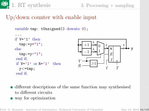
Up/down counter with enable input
variable tmp: tUnsigned(3 downto 0);
...if V=’1’ thentmp:=y+"1";
elsetmp:=y-"1";
end if;if V=’1’ or R=’1’ theny<=tmp;
end if;
4
4440
1
+1
−1
IRV ≥1
x y
I
T
E
different descriptions of the same function may synthesisedto different circuitsway for optimization
Prof. G. Kemnitz · Institute of Informatics, Technical University of Clausthal May 14, 2012 34/135

1. RT synthesis 3. Processing + sampling
Variables as data storage in sampling processes
signal T, x, y: STD LOGIC;
...process(T)variable z: STD LOGIC VECTOR(2 downto 0);
beginif RISING EDGE(T) theny <= z(2); z(2):=z(1);
z(1):=z(0); z(0):=x;
end if;end process;
z1 z2y
T
z0x
variables, which are read before assignment in the controlflow, store data for one clock period; behavior of a registervariables are only readable and writable within a process /can can not be used for terminal signals
Prof. G. Kemnitz · Institute of Informatics, Technical University of Clausthal May 14, 2012 35/135

1. RT synthesis 3. Processing + sampling
Behavior of conditional variable assignments
signal T, a, b, c, y0, y1: STD LOGIC;
...
process(T)variable v: STD LOGIC;
beginif RISING EDGE(T) thenA1: y0 <= v xor a;
if b=’1’ thenA2: v:= c;
end if;A3: y1 <= v xor a;
end if;
end process;
0
1c
T
a
b=1
=1
y0
y1
A1 und A2
variable vstatement
variable vstatement A3
A1: �v� is assigned at least one clock earlier (registeroutput)A3: �v� may be assigne in the same clock (register input)
Prof. G. Kemnitz · Institute of Informatics, Technical University of Clausthal May 14, 2012 36/135

1. RT synthesis 3. Processing + sampling
Variables that store data may represent in a synthesized circuitdifferent circuit points.
The description of registers by variables
is for that error-prone
should be used deliberately.
Prof. G. Kemnitz · Institute of Informatics, Technical University of Clausthal May 14, 2012 37/135
1. RT synthesis 4. Latches
Latches
Prof. G. Kemnitz · Institute of Informatics, Technical University of Clausthal May 14, 2012 38/135

1. RT synthesis 4. Latches
Latches, stage triggered memory element
signal E: STD LOGIC; signal x, y: tTyp;
...
process(x, E)
variable tE:DELAY LENGTH;
beginif E=’1’ theny <= invalid after th, x after td;
end if;--- check setup condition
if RISING EDGE(E) then
tE:=now;
elsif Falling EDGE(E) and (NOW-tE<tsor x’LAST EVENT<ts) theny <= invalid;
end if;end process;
tdtd
>ts>ts
th th
Lx
E
tTyp
E
x ytTyp
01
01
01
tTyp
VorhaltezeittsE Freigabeeingang
Verzogerungszeittdth Haltezeit
Bit- oder Bitvek-tortyp
x
E
y
Prof. G. Kemnitz · Institute of Informatics, Technical University of Clausthal May 14, 2012 39/135

1. RT synthesis 4. Latches
einfachere Schaltung als Register; genutzt zurAufwandsminimierungdas Freigabesignal ist zeit- und glitch-empfindlich
Die Synthesebeschreibungsschablone ist das stark vereinfachteSimulationsmodell:
ohne Zeitangabenohne Kontrolle der Vor- und Nachhaltebedingungenohne Berechnung der Gultigkeitsfenster
process(x, E)
beginif E=’1’ theny <= x;
end if;end process;
Auch wenn die Kontrollen fehlen, mussen die Vor- undNachhaltebedingungen erfullt sein.
Prof. G. Kemnitz · Institute of Informatics, Technical University of Clausthal May 14, 2012 40/135

1. RT synthesis 4. Latches
Die Tucken einer Latch-Schaltung am Beispiel
signal x1, x2, y:
std logic vector(n-1 downto 0);
...
process(x1, x2)
beginif x1=x2 theny <= x1;
end if;end process;
tdth
Lx
E
w3w1 w4
w2 w3
01E
x1
x2
y
==x2
x1
F1 F2
F1: moglich Invalidierung des gespeicherten WertesF2: moglicher Ubernahmefehler bei Ubereinstimmung
Prof. G. Kemnitz · Institute of Informatics, Technical University of Clausthal May 14, 2012 41/135

1. RT synthesis 4. Latches
Blockspeicher mit Latches
signal E: std logic;
signal a: std logic vector(1 downto 0);
signal x, s, q, y0, y1, y2, y3, s:
std logic vector(3 downto 0);
...
Dec:process(a)begincase a is
when "00" => s <= "0001";
when "01" => s <= "0010";
when "10" => s <= "0100";
when others => s <= "1000";
end case;
end process;
Ex
Ex
Ex
Ex
y1
y0
y2
y3
q0
q1
q2
q3
&
&
&
&
s0s1s2s3
Dec
x
E
00 10 01 1111
s0
s1
E
q0
q1
a
a
01
01
01
01
01
Prof. G. Kemnitz · Institute of Informatics, Technical University of Clausthal May 14, 2012 42/135

1. RT synthesis 4. Latches
Und:process(s, E)
beginif E=’1’ then q <= s;
else q <= "0000";
end if;
end process;
Latch0:process(x, q(0))
beginif q(0)=’1’ then y0<=x; end if;
end process;...
Ex
Ex
Ex
Ex
y1
y0
y2
y3
q0
q1
q2
q3
&
&
&
&
s0s1s2s3
Dec
x
E
a
Latch-Schaltungen sind nur mit einer bestimmten Struktur undAnsteuerung laufzeitrobust
UND-Verknupfung mit E unmittelbar vor denFreigabeeingangen der LatchesE muss inaktiv sein, wenn die Signale si invalid sindlaufzeitkritische Teile als vorentworfene Schaltungeneinbinden
Prof. G. Kemnitz · Institute of Informatics, Technical University of Clausthal May 14, 2012 43/135

1. RT synthesis 4. Latches
Latch zur Variablennachbildung inAbtastprozessen
signal T, a, b, c, y: std logic;
...
process(T)variable v: std logic;
beginif rising edge(T) then
if b=’1’ thenv:= c;
end if;y <= v xor a;
end if;
end process;
=1 ya
xE
c
bT
0
1=1 y
abT
c
bei einem Latch ist der Ubernahmewert sofort, nicht erst imFolgetakt am Ausgang verfugbar; erspart Multiplexerb muss mit Latch ein glitch-freies Abtastsignal seinProf. G. Kemnitz · Institute of Informatics, Technical University of Clausthal May 14, 2012 44/135

1. RT synthesis 5. Constraints
Constraints
Prof. G. Kemnitz · Institute of Informatics, Technical University of Clausthal May 14, 2012 45/135

1. RT synthesis 5. Constraints
Constraints
Zusatzinformationen fur die Synthese;Festlegungen/Empfehlungen fur
die Struktur und die Technologieabbildung (z.B. �keep�,um die Wegoptimierung bestimmter Signale undTeilschaltungen zu verbieten)die Platzierung (z.B. Zuordnung zwischen Anschlusssignalenund Schaltkreispins)maximale Verzogerungszeiten (Taktfrequenz oder -periode,Eingabe-Register-Verzogerung etc.)
Fur Praktikum (ise/Versuchsboard mit Xilinx-FPGA):Beschreibung der Pin-Zuordnung und der Taktfrequenz in derucf-Datei (user constraints file):
<loc> ..
Prof. G. Kemnitz · Institute of Informatics, Technical University of Clausthal May 14, 2012 46/135
1. RT synthesis 6. Entwurfsfehler
Entwurfsfehler
Prof. G. Kemnitz · Institute of Informatics, Technical University of Clausthal May 14, 2012 47/135

1. RT synthesis 6. Entwurfsfehler
Entwurfsfehler und Fehlervermeidung
Synthesebeschreibungen haben ihre typischen Entwurfsfehler,darunter auch einige die nur das Zeitverhalten und/oder dieZuverlassigkeit der synthetisierten Schaltung beeintrachtigen unddadurch schwer zu finden sind.
Prof. G. Kemnitz · Institute of Informatics, Technical University of Clausthal May 14, 2012 48/135

1. RT synthesis 6. Entwurfsfehler
Speicherverhalten in kombinatorischen Prozessen
x1
x2y
z
not z;
not sz;not z;
zb;not
&
0
1
0
1
0
1
0
1
0
1
0
1process
begin
end process;
(x1);variable
process
begin
end process;
(x1, x2);
sz <= x1 and x2;
processvariable
begin
end process;
z := x1 and x2;
(x1, x2);
y <=
yF2 <=
z := x1
(x1, x2);processvariable
begin
end process;z := x1
and x2;
and x2;yF3 <=
yF1 <=
x2
x1
y
yF1
yF2
yF3
signal x1, x2, sz, y, yF1, yF2, yF3:
z: z:
z:
FehlverhaltenSoll-Verhalten
F2 F3
F1korrekt
warte
;
; ;
;
STD LOGIC
STD LOGIC STD LOGIC
STD LOGIC
F1: fehlendes Signal in der Weckliste; F2: Signal statt Variableals Zwischenspeicher; F3: Variablenwert vor der Zuweisungausgewertet
Prof. G. Kemnitz · Institute of Informatics, Technical University of Clausthal May 14, 2012 49/135

1. RT synthesis 6. Entwurfsfehler
Fallunterscheidung mit fehlender Zuweisung
signal x1, x2, x3 y: std logic vector(3 downto 0);
signal s: std logic vector(1 downto 0);
...process(s, x1, x2, x3)
begincase s iswhen "00" => y <= x1;
when "01" => y <= x2;
when "10" => y <= x3;
when others => null;--- Korrektur: y <= x3 statt null
end case;end process;
4
4
4
4
4
4
4
400x1
01
sonstx3
x2 y
s2
&s
yLx
E
00x1
01
10x3
x2
2
auch wenn ein Auswahlwert nicht auftreten kann, ist in einerMultiplexerbeschreibung ein Wert zuzuweisen
Prof. G. Kemnitz · Institute of Informatics, Technical University of Clausthal May 14, 2012 50/135

1. RT synthesis 6. Entwurfsfehler
Fehlersymptome:
nicht synthetisierbar oder unerwarteter Latch-Einbau
Fehlervermeidung
Verwendung der Kurzform �nebenlaufige Signalzuweisung�,im Beispiel aus UND und Inverter:
y <= not (x1 and x2);
spater fur beliebig komplexe kombinatorische Schaltungen:
signal x: tEingabe;
signal y: tAusgabe;
function f(x: tEingabe) return tAusgabe;
...
y <= invalid after th, f(x), after td ;
Synthesebeschreibung ohne grau unterlegte Teilenebenlaufige Signalzuweisungen und Funktionen konnen keinSpeicherverhalten beschreiben / keinen der skizziertenFehler enthalten
Prof. G. Kemnitz · Institute of Informatics, Technical University of Clausthal May 14, 2012 51/135

1. RT synthesis 6. Entwurfsfehler
Bosartige Timing-Probleme
Symptome:
zulassige Taktfrequenz laut Synthsereport zu niedrig
messbare Zeitprobleme an den Anschlusssignalen
Anderung der Beschreibung zeigt keine Wirkung
Fehlerwirkung nicht mit Simulation nachstellbar / nichtreproduzierbar
Ursache sind in der Regel fehlende oder falsche Zeit-Constraints
Constraint-Doku lesen und Constraints richtig beschreiben
Prof. G. Kemnitz · Institute of Informatics, Technical University of Clausthal May 14, 2012 52/135

1. RT synthesis 6. Entwurfsfehler
Gutartige Timing-Probleme
Symptome:
Zusatzverzogerungen um ganze Taktperioden
Fehlerwirkung mit Simulation nachstellbar
typische Ursachen
Zwischenergebnisse in Abtastprozessen in Signalen stattVariablen weitergereicht
Variablenwerte vor der Wertzuweisung ausgewertet
Denkfehler im Algorithmus und in der Ablaufplanung
Prof. G. Kemnitz · Institute of Informatics, Technical University of Clausthal May 14, 2012 53/135

1. RT synthesis 6. Entwurfsfehler
Nicht synthetisierbar
ungeeignete Funktion, z.B. kein gerichteter Berechnungsfluss
x2x3
0110
0 0setzen
speichern
y
rucksetzen
t2 · td
td
Gesamtschaltung x1 = 0 x1 = 1, x2 = x3 = 0
0
1y
G1 G2 G3y
≥1
G1
=1
≥1 ≥1
≥1
G2G3
yx1
x2
x3
G2G3
x2
x3
a)
b)
c)
y
Speicher- oder Schwingungsverhalten bei der Simulation
ungeeignete Beschreibungsstruktur
Wenn das simulierte Verhalten ok. ist, ausweichen aufbewahrte Beschreibungsschablonen (Doku desSyntheseprogramms lesen)
Prof. G. Kemnitz · Institute of Informatics, Technical University of Clausthal May 14, 2012 54/135
1. RT synthesis 7. Zusammenfassungf
Zusammenfassungf
Prof. G. Kemnitz · Institute of Informatics, Technical University of Clausthal May 14, 2012 55/135
1. RT synthesis 7. Zusammenfassungf
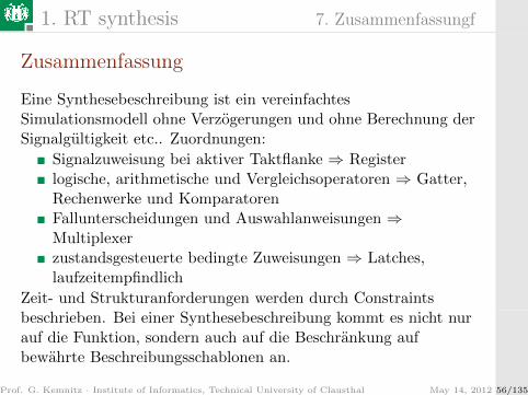
Zusammenfassung
Eine Synthesebeschreibung ist ein vereinfachtesSimulationsmodell ohne Verzogerungen und ohne Berechnung derSignalgultigkeit etc.. Zuordnungen:
Signalzuweisung bei aktiver Taktflanke ⇒ Registerlogische, arithmetische und Vergleichsoperatoren ⇒ Gatter,Rechenwerke und KomparatorenFallunterscheidungen und Auswahlanweisungen ⇒Multiplexerzustandsgesteuerte bedingte Zuweisungen ⇒ Latches,laufzeitempfindlich
Zeit- und Strukturanforderungen werden durch Constraintsbeschrieben. Bei einer Synthesebeschreibung kommt es nicht nurauf die Funktion, sondern auch auf die Beschrankung aufbewahrte Beschreibungsschablonen an.
Prof. G. Kemnitz · Institute of Informatics, Technical University of Clausthal May 14, 2012 56/135

1. RT synthesis 8. Aufgaben
Aufgaben
Prof. G. Kemnitz · Institute of Informatics, Technical University of Clausthal May 14, 2012 57/135

1. RT synthesis 8. Aufgaben
Aufgabe 2.1: Registerextraktion
signal K,L,M,N,P,Q: std logic vector(7 downto 0);
signal c: std logic vector(1 downto 0);
process(c(0))beginif rising edge(c(0)) thenL <= K;
end if;end process;
process(c(1))beginif rising edge(c(1)) thenN<=M; M<=L;
end if;end process;
process(c(1))beginif falling edge(c(1)) thenP<=L; Q<=P;
end if;end process;
Anschlusssignale,Ubernahmebedingungenetc. aller beschriebenenRegister suchen
Signalflussplan zeichnen
Prof. G. Kemnitz · Institute of Informatics, Technical University of Clausthal May 14, 2012 58/135

1. RT synthesis 8. Aufgaben
Aufgabe 2.2: Beschreibung als synthesefahigerkombinatorischer Prozess
01
01 +
≥1
&
01
y
s1
4
4
tUnsigned(3 downto 0)
STD LOGIC4
44
4
4
ab
s0
44
44
Prof. G. Kemnitz · Institute of Informatics, Technical University of Clausthal May 14, 2012 59/135
1. RT synthesis 8. Aufgaben
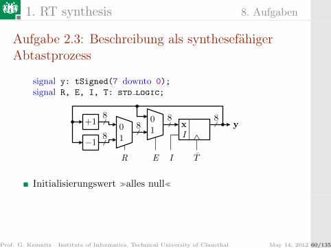
Aufgabe 2.3: Beschreibung als synthesefahigerAbtastprozess
signal y: tSigned(7 downto 0);
signal R, E, I, T: std logic;
+1
−1
01
01
yxI
8
88
8 8
R E I T
Initialisierungswert �alles null�
Prof. G. Kemnitz · Institute of Informatics, Technical University of Clausthal May 14, 2012 60/135

1. RT synthesis 8. Aufgaben
Aufgabe 2.4: Synthesefahige Beschreibung mitmoglichst wenig Prozessen
signal T, I, x, x del, y: std logic;
IxI
x’
Reg2GReg1
==
T
xy
Initialwert �0�
Prof. G. Kemnitz · Institute of Informatics, Technical University of Clausthal May 14, 2012 61/135

1. RT synthesis 8. Aufgaben
Aufgabe 2.5: Synthesefahige Beschreibung desAutomaten
0100
1011
00011011
000110
11
00
011011
00 01 10
00011011
000110
11
00
011011
00 01 10
d)
s x :
s+ = fs(x, s)y
x xI
ss+
2
2
2
y = fa(x, s)fa(x, s)
I T
fs(x, s)
Prof. G. Kemnitz · Institute of Informatics, Technical University of Clausthal May 14, 2012 62/135

1. RT synthesis 8. Aufgaben
Aufgabe 2.6: Extraktion des Signalflussplans
signal x, tmp, acc, y: std logic vector(3 downto 0);
signal op: std logic vector(1 downto 0);
signal T: std logic;...
process(T)beginif rising edge(T) thencase op iswhen "00" => acc <= x;
when "01" => acc <= acc + tmp;
when "10" => acc <= acc - tmp;
when others => null;end case;
end if;tmp <= x;
end process;
y <= acc;Prof. G. Kemnitz · Institute of Informatics, Technical University of Clausthal May 14, 2012 63/135

2. Logikoptimierung
Logikoptimierung
Prof. G. Kemnitz · Institute of Informatics, Technical University of Clausthal May 14, 2012 64/135

2. Logikoptimierung
Definition 1
Eine n-stellige logische Funktion ist eine Abbildung einesn-Bit-Vektors aus freien binaren Variablen auf eine abhangigebinare Variable:
f : Bn → B mit B = {0, 1}bzw.
y = f (xn−1, xn−2, . . . , x0) mit y, xi ∈ {0, 1}
(y – abhangige Variable; xi freie Variablen).
Jede logische Funktion kann durch praktisch unbegrenztviele logische Ausdrucke und Schaltungen nachgebildetwerden.Die Register-Transfer-Synthese extrahiert logischeFunktionen in Form von kombinatorischenTeilschaltungsbeschreibungen.
Prof. G. Kemnitz · Institute of Informatics, Technical University of Clausthal May 14, 2012 65/135

2. Logikoptimierung
Anschließende Vereinfachung:
Vereinfachung logischer Ausdrucke mit Hilfe derSchaltalgebra (dieser Abschnitt)Darstellung der logischen Ausdrucke zur Vereinfachung alsbinare Entscheidungsdiagramme (nachster Abschnitt).
Bereits behandelte Vereinfachungstechniken:
Konstanteneliminationbeseitigt alle Operationen, bei denen freie Variablen mitkonstanten Werten belegt sind; reduziert die Stelligkeit unddie Anzahl der OperationenVerschmelzungfasst gleiche Berechnungsschritte mit gleichen Operandenzusammen und reduziert so die Anzahl der Operationen
Prof. G. Kemnitz · Institute of Informatics, Technical University of Clausthal May 14, 2012 66/135

2. Logikoptimierung 1. Umformungsregeln
Umformungsregeln
Prof. G. Kemnitz · Institute of Informatics, Technical University of Clausthal May 14, 2012 67/135
2. Logikoptimierung 1. Umformungsregeln
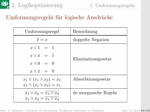
Umformungsregeln fur logische Ausdrucke
Umformungsregel Bezeichnung
¯x = x doppelte Negation
x ∨ 1 = 1
x ∨ x = 1
x ∧ 0 = 0
x ∧ x = 0
Eliminationsgesetze
x1 ∨ (x1 ∧ x2) = x1x1 ∧ (x1 ∨ x2) = x1
Absorbtionsgesetze
x1 ∨ x2 = x1 ∧ x2x1 ∧ x2 = x1 ∨ x2
de morgansche Regeln
Prof. G. Kemnitz · Institute of Informatics, Technical University of Clausthal May 14, 2012 68/135
2. Logikoptimierung 1. Umformungsregeln
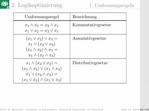
Umformungsregel Bezeichnung
x1 ∧ x2 = x2 ∧ x1x1 ∨ x2 = x2 ∨ x1
Kommutativgesetze
(x1 ∨ x2) ∨ x3 =x1 ∨ (x2 ∨ x3)
(x1 ∧ x2) ∧ x3 =x1 ∧ (x2 ∧ x3)
Assoziativgesetze
x1 ∧ (x2 ∨ x3) =(x1 ∧ x2) ∨ (x1 ∧ x3)x1 ∨ (x2 ∧ x3) =
(x1 ∨ x2) ∧ (x1 ∨ x3)
Distributivgesetze
Prof. G. Kemnitz · Institute of Informatics, Technical University of Clausthal May 14, 2012 69/135

2. Logikoptimierung 1. Umformungsregeln
Beweis der Umformungsregeln
Aufstellen und Vergleich der Wertetabellen.
Fur die de morganschen Regeln gilt z.B.:
x1 x2 x1 ∨ x2 x1 ∧ x2 x1 ∧ x2 x1 ∨ x2
0 0 1 1 1 1
0 1 1 1 0 0
1 0 1 1 0 0
1 1 0 0 0 0
Prof. G. Kemnitz · Institute of Informatics, Technical University of Clausthal May 14, 2012 70/135
2. Logikoptimierung 1. Umformungsregeln
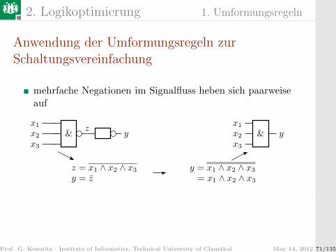
Anwendung der Umformungsregeln zurSchaltungsvereinfachung
mehrfache Negationen im Signalfluss heben sich paarweiseauf
z = x1 ∧ x2 ∧ x3
y = z
&x1
x2
x3
&x1
x2
x3
yyz
y = x1 ∧ x2 ∧ x3
= x1 ∧ x2 ∧ x3
Prof. G. Kemnitz · Institute of Informatics, Technical University of Clausthal May 14, 2012 71/135

2. Logikoptimierung 1. Umformungsregeln
doppelte Anwendung der Eliminationsgesetze
& y1
y = (x1 ∧ x1︸ ︷︷ ︸0
) ∧ x2 = 0 ∧ x2︸ ︷︷ ︸0
= 0 = 1
x2
x1 y
Prof. G. Kemnitz · Institute of Informatics, Technical University of Clausthal May 14, 2012 72/135

2. Logikoptimierung 1. Umformungsregeln
Anwendung des Absorbtionsgesetzes
&
&
≥1
&x1
x2y
Assoziativgesetz:Absorbtionsgesetz:
gegeben Funktion: y = (x1 ∧ x2) ∧ (x2 ∨ x3)y = x1 ∧ (x2 ∧ (x2 ∨ x3))y = x1 ∧ x2
x1
x2
x3
y
Suchproblem: in gegebenen AusdruckenAnwendungsmoglichkeiten fur die Gesetze finden
Prof. G. Kemnitz · Institute of Informatics, Technical University of Clausthal May 14, 2012 73/135
2. Logikoptimierung 1. Umformungsregeln
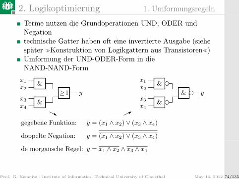
Terme nutzen die Grundoperationen UND, ODER undNegationtechnische Gatter haben oft eine invertierte Ausgabe (siehespater �Konstruktion von Logikgattern aus Transistoren�)Umformung der UND-ODER-Form in dieNAND-NAND-Form
x1
x2
x3
x4
&
≥1
&
x1
x2
x3
x4
&
&
&y y
y = (x1 ∧ x2) ∨ (x3 ∧ x4)
y = (x1 ∧ x2) ∨ (x3 ∧ x4)
y = x1 ∧ x2 ∧ x3 ∧ x4de morgansche Regel:
doppelte Negation:
gegebene Funktion:
Prof. G. Kemnitz · Institute of Informatics, Technical University of Clausthal May 14, 2012 74/135

2. Logikoptimierung 1. Umformungsregeln
Umformung der ODER-UND-Form in die NOR-NOR-Form
≥1
≥1
&
x1
x2
x3
x4
x1
x2
x3
x4≥1
≥1
≥1
yy
y = (x1 ∨ x2) ∧ (x3 ∨ x4)
y = (x1 ∨ x2) ∧ (x3 ∨ x4)
y = x1 ∨ x2 ∨ x3 ∨ x4
gegebene Funktion:
doppelte Negation:
de morgansche Regel:
Prof. G. Kemnitz · Institute of Informatics, Technical University of Clausthal May 14, 2012 75/135

2. Logikoptimierung 2. Optimierungsziele
Optimierungsziele
Prof. G. Kemnitz · Institute of Informatics, Technical University of Clausthal May 14, 2012 76/135

2. Logikoptimierung 2. Optimierungsziele
Optimierungsziele
minimale Gatteranzahl
minimale Chipflache
minimaler Stromverbrauch
minimale Verzogerung etc.
Regel zur Geschwindigkeitsoptimierung: Baume statt Ketten
Pfad der langsten Verzogerung
tdOp tdOp tdOp tdOptdOp tdOp
tdOp
tdOp
tdOp
x0
x1
x2 x3 x5 x6x4
y y
x0
x1
x6
x5
x4
x3
x2
tdKette = n · tdOp
tdBaum ≥ log2(n) · tdOp
b)a)
◦ assoziative Operation (Zusammenfassungsreihenfolge vertauschbar)
Prof. G. Kemnitz · Institute of Informatics, Technical University of Clausthal May 14, 2012 77/135

2. Logikoptimierung 2. Optimierungsziele
oft unterscheiden sich die Losungen fur minimalen Aufwand undmax. Geschwindigkeit etc.
langster Pfad
=1
=1
=1
y2
y1
y0
x3
x2
x1
x0
a)
=1=1
=1=1
x2
x1
x0
x3
y0y1
y2c)
b)
te Losungen
Verzogerungminimale
minimalerAufwand
Aufwand
andere optimier-
max
minmin max
Signalverzogerung
Prof. G. Kemnitz · Institute of Informatics, Technical University of Clausthal May 14, 2012 78/135

2. Logikoptimierung 3. Konjunktionsmengen
Konjunktionsmengen
Prof. G. Kemnitz · Institute of Informatics, Technical University of Clausthal May 14, 2012 79/135

2. Logikoptimierung 3. Konjunktionsmengen
Logikminimierung mit Konjunktionsmengen
klassische Verfahren
KV-Diagramm: graphisches VerfahrenQuine-McCluskey: gleicher Algorithmus als Suchproblem
Konjunktion: Term, der direkte oder invertierteEingabevariablen UND-verknupft, z.B.:
x3 ∧ x2 ∧ x1 ∧ x0 = x3x2x1x0 (K1010)︸ ︷︷ ︸verkurzte Schreibweisen
Minterm: Konjunktion, die alle Eingabevariablen entweder indirekter oder in negierter Form enthalt.
Satz: Jede logische Funktion lasst sich durch eine Mengevon Konjunktionen darstellen, die ODER-verknupftwerden.
Prof. G. Kemnitz · Institute of Informatics, Technical University of Clausthal May 14, 2012 80/135

2. Logikoptimierung 3. Konjunktionsmengen
Beweis: Jede logische Funktion lasst sich durch eineWertetabelle darstellen. Jeder Zeile einerWertetabelle ist ein Minterm zugeordnet, der genaudann Eins ist, wenn die Zeile ausgewahlt ist.
Die Funktion ist entweder die
ODER-Verknupfung der Minterme, fur die y = 1 ist
xn−1 x0x1x2
· · ·
(programmierbar)ODER-Matrix
y0 y1 y2 ym−1
· · ·
(1 aus 2n - Decoder)UND-Matrix
2n vollstandige Konjunk-tionen (Produktterme)
· · ·
negierte ODER-Verknupfung der Minterme, fur die y = 0 ist.
Prof. G. Kemnitz · Institute of Informatics, Technical University of Clausthal May 14, 2012 81/135

2. Logikoptimierung 3. Konjunktionsmengen
x2 x1 x0 Konjunktion y x2 x1 x0 Konjunktion y
0 0 0 x2x1x0 (K000) 0 1 0 0 x2x1x0 (K100) 1
0 0 1 x2x1x0 (K001) 1 1 0 1 x2x1x0 (K101) 1
0 1 0 x2x1x0 (K010) 0 1 1 0 x2x1x0 (K110) 1
0 1 1 x2x1x0 (K011) 0 1 1 1 x2x1x0 (K111) 0
Entwicklung nach den Einsen: {K001, K100, K101, K110} ⇒y = x2x1x0 ∨ x2x1x0 ∨ x2x1x0 ∨ x2x1x0
Entwicklung nach den Nullen: {K000, K010, K011, K111} ⇒y = x2x1x0 ∨ x2x1x0 ∨ x2x1x0 ∨ x2x1x0
= x2x1x0 ∧ x2x1x0 ∧ x2x1x0 ∧ x2x1x0
= (x2 ∨ x1 ∨ x0) (x2 ∨ x1 ∨ x0) (x2 ∨ x1 ∨ x0) (x2 ∨ x1 ∨ x0)
Prof. G. Kemnitz · Institute of Informatics, Technical University of Clausthal May 14, 2012 82/135

2. Logikoptimierung 3. Konjunktionsmengen
Vereinfachungsgrundlage
Satz: Zwei Konjunktionen, die sich nur in derInvertierung einer Variablen unterscheiden, konnenzu einer Konjunktion mit einer Variablen wenigerzusammengefasst werden.
Schritt ODER-Verknupfung Konjunktionsmenge
1 . . . ∨ x2x1x0 ∨ x2x1x0 ∨ . . . {. . . , K100, K101, . . .}2 . . . ∨ x2x1 (x0 ∨ x0) ∨ . . .
3 . . . ∨ x2x1 ∨ . . . {. . . , K10∗, . . .}
nur Abweichung in Stelle EinsWert von x1 �don’t care�, in VHDL ’-’eine Konjunktion weniger
Prof. G. Kemnitz · Institute of Informatics, Technical University of Clausthal May 14, 2012 83/135

2. Logikoptimierung 4. KV-Diagramme
KV-Diagramme
Prof. G. Kemnitz · Institute of Informatics, Technical University of Clausthal May 14, 2012 84/135
2. Logikoptimierung 4. KV-Diagramme
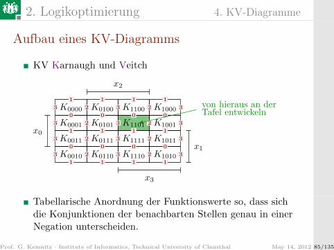
Aufbau eines KV-Diagramms
KV Karnaugh und Veitch
K0010
K0011
K0001
K0000 K0100
K0101
K0111
K0110
K1100
K1101
K1111
K1000
K1001
K1010
K1011
K11102
2
2
2
2
2
2
2
3
3
3
3
3
3
3
3
3
3
3
3
0 0 0 0
0 0 0 0
1 1 1 1
1 1 1 1
1 1 1 1
x0
x1
x3
x2
Tafel entwickelnvon hieraus an der
Tabellarische Anordnung der Funktionswerte so, dass sichdie Konjunktionen der benachbarten Stellen genau in einerNegation unterscheiden.
Prof. G. Kemnitz · Institute of Informatics, Technical University of Clausthal May 14, 2012 85/135

2. Logikoptimierung 4. KV-Diagramme
Zusammenfassen der ausgewahlten Konjunktionen zuBlocken der Kantenlange eins, zwei oder vier:
K000-
K-11-
K10--
K-10-
y = 0y = 1
K0010
K0011
K0001
K0000 K0100
K0101
K0111
K0110
K1100
K1101
K1111
K1000
K1001
K1010
K1011
K1110
K001-
2
2
2
2
2
2
2
2
3
3
3
3
3
3
3
3
3
3
3
3
0 0 0 0
0 0 0 0
1 1 1 1
1 1 1 1
1 1 1 1
x0
x1
x3
x2
Minimierte Konjunktionsmenge der Einsen
{K000-, K-11-, K10--} ⇒ y = x3x2x1 ∨ x2x1 ∨ x3x2
Minimierte Konjunktionsmenge der Nullen:
{K001-, K-10-} ⇒ y = x3x2x1 ∨ x2x1Prof. G. Kemnitz · Institute of Informatics, Technical University of Clausthal May 14, 2012 86/135

2. Logikoptimierung 4. KV-Diagramme
Praktische Arbeit mit KV-Diagrammen
Geordnete Tabelle mit FunktionswertenOptimierungsziel: moglichst große und moglichst wenigeBlockeBlocke durfen sich uberlagern
x0
x1
x2
x3
0
1 1 1
1
1
1
0 0
0
0
000
0 0
d
b
c
d
a
a: x3x1x0
b: x2x1x0
c: x3x2x0
y = x3x1x0 ∨ x3x1x0 ∨ x3x2x0 ∨ x3x2x0
d: x3x2x0
Prof. G. Kemnitz · Institute of Informatics, Technical University of Clausthal May 14, 2012 87/135
2. Logikoptimierung 4. KV-Diagramme
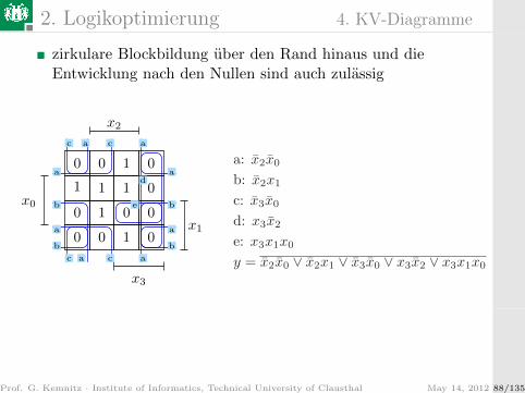
zirkulare Blockbildung uber den Rand hinaus und dieEntwicklung nach den Nullen sind auch zulassig
x0
x2
x3
0
1 1 1
1
1
1
0 0
0
0
000
0 0x1
d
e
a
c a c a
a
b
a
c a
b
bb
a c
a
y = x2x0 ∨ x2x1 ∨ x3x0 ∨ x3x2 ∨ x3x1x0
a: x2x0
b: x2x1
c: x3x0
d: x3x2
e: x3x1x0
Prof. G. Kemnitz · Institute of Informatics, Technical University of Clausthal May 14, 2012 88/135

2. Logikoptimierung 4. KV-Diagramme
KV-Diagramme mit don’t-care-Feldern
don’t-care-Felder kennzeichnen Eingabemoglichkeiten, dieim normalen Betrieb nicht auftretenihr Wert wird so festgelegt, dass sich moglichst wenige undmoglichst große Blocke bilden lassen
x2
x1
x3
x0
1
1
0
00
0
1 1 -
-
-
-
0
1
1
1
b c
d
a
e
d a: x1x0
b: x2x1x0
c: x3x1x0
d: x3x2x0
e: x3x2x1
y = x1x0 ∨ x2x1x0 ∨ x3x1x0
∨x3x2x0 ∨ x3x2x1
Prof. G. Kemnitz · Institute of Informatics, Technical University of Clausthal May 14, 2012 89/135

2. Logikoptimierung 4. KV-Diagramme
KV-Diagramme fur zwei- und dreistelligeFunktionen
Verringerung der Anzahl der Nachbarfelder, die sich in einerNegation unterscheiden auf drei bzw. zweiHalbierung der Hohe und/oder der Breite
K001
K000 K010
K011
K110
K111
K100
K101
K010
K011
K001
K000 K100
K101
K111
K110
K01
K10
K11
K00
0 0 0 0
0
0
0
0
2
2
2
2
0 0
1
1
2 2 2
2 2 2
1 1
1 1
1
1
1
1
1
1
x0
x1
x0
x1
x2
x0
x1
x2
Prof. G. Kemnitz · Institute of Informatics, Technical University of Clausthal May 14, 2012 90/135
2. Logikoptimierung 4. KV-Diagramme
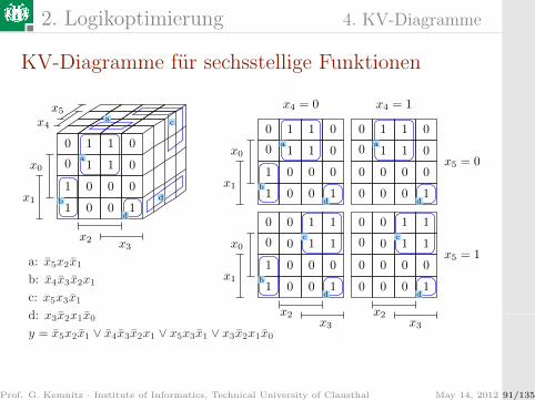
KV-Diagramme fur sechsstellige Funktionen
x0
x1
x2 x3
x0
x1
x0
x1
x2x3
x2x3
0
1 1
1 0
0
0
0
0
1
1
1
0
0
0 1
0
1 1
1 0
0
0
0
0
1
1
1
0
0
0 10
1
1
0
0
01
1
0
0
0 1
0
0 1
1
0
1
1
0
0
00
0
0 1
0
0
0
0
1
1
0
1 1
1 0
0
0
0
0
1
0
0
0 1
0
0
x4
x5x4 = 0 x4 = 1
x5 = 0
x5 = 1
b
c
d
a
b
d
a
b
c
d
d
c
d
a
d
a
a: x5x2x1
b: x4x3x2x1
c: x5x3x1
d: x3x2x1x0
y = x5x2x1 ∨ x4x3x2x1 ∨ x5x3x1 ∨ x3x2x1x0
Prof. G. Kemnitz · Institute of Informatics, Technical University of Clausthal May 14, 2012 91/135
2. Logikoptimierung 4. KV-Diagramme
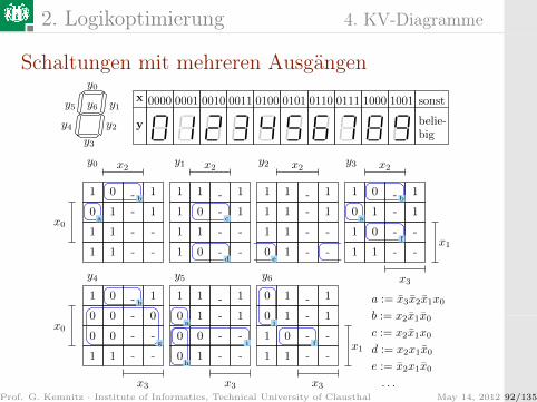
Schaltungen mit mehreren Ausgangen
x
y
x0
x0
x1
x1
x2 x2 x2 x2
x3
x3x3x3
y0
y2y4
y6
y3
y1y5 0000 0001 0010 0011 0100 0101 0110 0111 1000 1001
belie-
sonst
big
0
01
1
11
1 1
1
1-
-
-
-
-
-
0
0
0
1
1
1
11
1
1
-
-
-
-
-
-0
1
1
1 1
1
1 1
1
1
-
-
-
-
-
-
1
1
1
1
1
1 1
10
0
-
-
-
-
-
-
0
0
01
1 1
1
1 1
1
-
-
-
-
-
-
. . .
1
10
0 0
00
-
-
-
-
-
-
1
0
1
0
0
0 0
1 1
1
1
1
1-
-
-
-
-
-
y0 y1 y2 y3
y4 y5 y6
a := x3x2x1x0
b := x2x1x0
c := x2x1x0
d := x2x1x0
e := x2x1x0
a
b
a
b
f
e
c
d
j
f
b
a
h
ig
Prof. G. Kemnitz · Institute of Informatics, Technical University of Clausthal May 14, 2012 92/135

2. Logikoptimierung 4. KV-Diagramme
signal x: std logic vector(3 downto 0);
signal y: std logic vector(6 downto 0);
...process(x)variable a,b,c,d,e,f,g,h,i,j: std logic;
begina := not x(3) and not x(2) and not x(1) and x(0);
b := x(2) and not x(1) and not x(0);
c := x(2) and not x(1) and x(0);
d := x(2) and x(1) and not x(0);
e := not x(2) and x(1) and not x(0);
...
y(0)<=not(a or b);
y(1)<=not(c or d);
y(2)<=not e;
...
end process;
x3x3x3
x0
x2 x2 x2
x1
0
01
1
11
1 1
1
1-
-
-
-
-
- 0
1
1
1 1
1
1 1
1
1
-
-
-
-
-
-
1
1
1
1
1
1 1
10
0
-
-
-
-
-
-
y0 y1 y2
a
b
e
c
d
Prof. G. Kemnitz · Institute of Informatics, Technical University of Clausthal May 14, 2012 93/135

2. Logikoptimierung 4. KV-Diagramme
Beispiel fur einen Automatenentwurf
R/N
A B
CD
V/L
R/LV/KR/K
V/M
R/M
V/NH/N H/M
H/LH/K
00(A)01(B)10(C)11(D)
01(H)00(V)
00(A)
01(B)10(C)11(D)
01(H)
00(K)01(L)10(M)11(N)
00(V)
01(L)10(M)11(N)00(K)
10(R)
11(N)00(K)01(L)10(M)
V, A, KSymbol H, B, L R, C, M D, N
s, s+y
Zustand, Folgezustand (je 2 Bit)Eingabesignal (2 Bit)x
Ausgabesignal
a) b)
c)
10(R)
11(D)00(A)01(B)10(C)
s+ = fs(x, s)
01(B)00(A)
10(C)11(D)
s x
00Code 01 10 11
symbolische Eingabewertesymbolische Zustande
V, H, RA, B, C, D
symbolische AusgabewerteK, L, M, N
y = fa(x, s)
Zustandscodierung ist so gewahlt, dass y = s+ gilt
Prof. G. Kemnitz · Institute of Informatics, Technical University of Clausthal May 14, 2012 94/135
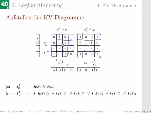
2. Logikoptimierung 4. KV-Diagramme
Aufstellen der KV-Diagramme
s1 s1
x1
x0
s0 s0
0
1
0
1 0 1
0 1
- - - -
1
1 1
0
0
1 0 1
0
- - - -
1 0 0 1
s+0 = y0s+1 = y1
0
V
H
R
-
A B D C A B D C
0 1aa
b
aaa
d
c
b e
y0 = s+0 = s0x0 ∨ s0x0
y1 = s+1 = s1s0x1x0 ∨ s1s0x1 ∨ s1s0x1 ∨ s1x1x0 ∨ s1s0x1 ∨ s1x0
Prof. G. Kemnitz · Institute of Informatics, Technical University of Clausthal May 14, 2012 95/135

2. Logikoptimierung 4. KV-Diagramme
Vom KV-Diagramm zur Schaltung
Auswahl der zu verwendenden Gatter und Speicherzellen(Technologieabbildung)
Beispielbausteinsystem: Inverter + NAND-Gatter mitunterschiedlicher Eingangsanzahl + 1-Bit-Register mitRucksetzeingangGleichungsumformung mit de morganscher Regel
y0 = s+0 = s0x0 ∨ s0x0 = (s0x0) (s0x0)
y1 = s+1 = s1s0x1x0 ∨ s1s0x1 ∨ s1s0x1 ∨ s1x1x0 ∨ s1s0x1 ∨ s1x0
= (s1s0x1x0) (s1s0x1) (s1s0x1) (s1s0x1) (s1x0)
Prof. G. Kemnitz · Institute of Informatics, Technical University of Clausthal May 14, 2012 96/135

2. Logikoptimierung 4. KV-Diagramme
y0 = s+0 = (s0x0) (s0x0)
y1 = s+1 = (s1s0x1x0) (s1s0x1) (s1s0x1) (s1s0x1) (s1x0)
&Rx
s0s0 x1x1s1s1 x0x0
Rx
s0
y0
&
&
&
&
&
&
&
y1
s1&
x0
x1
I
T⇒Web-Projekt:
P2.2/Test VRZ.vhdl
Prof. G. Kemnitz · Institute of Informatics, Technical University of Clausthal May 14, 2012 97/135

2. Logikoptimierung 5. Quine und McCluskey
Quine und McCluskey
Prof. G. Kemnitz · Institute of Informatics, Technical University of Clausthal May 14, 2012 98/135

2. Logikoptimierung 5. Quine und McCluskey
Optimierung nach Quine & McCluskey – Prinzip
Alternatives tabellenbasiertes Minimierungsverfahren, dasgleichfalls auf der Zusammenfassung von Konjunktionen, die sichnur in einer Negation unterscheiden, basiert:
{. . . , K100, K101, . . .} ⇒ {. . . , K10∗, . . .}Zusammenstellen der Menge aller Minterme, fur die derFunktionswert Eins (bzw. Null) ist ⇒ quinesche Tabellenullter OrdnungSuche in der quineschen Tabelle nullter Ordnung alleMoglichkeiten zur Bildung einer Konjunktion mit einerdon’t-care-Stelle und abhaken der erfassten Konjunktionen⇒ quinesche Tabelle erster Ordnungetc.Ausdrucksminimierung mit Hilfe der Abdeckungstabelle derPrimterme
Prof. G. Kemnitz · Institute of Informatics, Technical University of Clausthal May 14, 2012 99/135

2. Logikoptimierung 5. Quine und McCluskey
Aufstellen der quineschen Tabellen
x0
x1
x2
x3
0
1
3
2
4
5
7
6
8
9
10
11
12
13
14
15
2 01008 1 0 0 0
3 1 1005 1 10010 1 10 012 1 1 0 0
7 1 1 1013 1 1 1014 1 1 1 0
100 -2, 3102, 10 - 0
8, 12 1 0 0-1 0 0-8, 10
1 10 -3, 71 10 -5, 71 1- 05, 13
1 1 0-12, 141 1 0 -12, 131 1 0-10, 14
1 - 0-8, 10, 12, 14
x1x2x3 x0 x1x2x3 x0
x1x2x3 x0
Visualisierung der Block-bildungsmoglichkeiten
mit einem KV-Diagramm
√√
nullte Ordnungquinesche Tabelle
√√√√√√√
erste und zweite Ordnungquinesche Tabellen
√
√
√
P1
P2
P3
P7
P6
P5
P4
√
moglicher Vierererblockmogliche Zweierblocke
√abgedeckte Konjunktionen
PrimtermPi
2
3
4
5
6
7
1
1
Prof. G. Kemnitz · Institute of Informatics, Technical University of Clausthal May 14, 2012 100/135

2. Logikoptimierung 5. Quine und McCluskey
die Konjunktionen sind in den quineschen Tabellen nach derAnzahl der Einsen im zugehorigen Bitvektor geordnet
Zusammenfassung nur moglich, wenn sich die Anzahl derEinsen genau um Eins unterscheidet.
Abhaken der Konjunktionen mitZusammenfassungsmoglichkeit
Prof. G. Kemnitz · Institute of Informatics, Technical University of Clausthal May 14, 2012 101/135

2. Logikoptimierung 5. Quine und McCluskey
Auswahl der PrimtermeAufstellen der AbdeckungstabelleSuche einer minimalen Abdeckungsmenge
x0
x2
x3
x1
0
1
3
2
4
5
7
6
8
9
10
11
12
13
14
15
genutzte Primterme ungenutzte Primterme
2 3 5 7 8 10 12 13 14
P7
P3
P4
P6
P2
P1
P5
1
1
2
3
4
5
6
7
Losungsmenge: {P1, P2, P5, P7}:y = x3x0︸︷︷︸
P1
∨ x3x2x1︸ ︷︷ ︸P2
∨x3x2x0︸ ︷︷ ︸P5
∨x3x2x1︸ ︷︷ ︸P7
Prof. G. Kemnitz · Institute of Informatics, Technical University of Clausthal May 14, 2012 102/135

2. Logikoptimierung 5. Quine und McCluskey
Die quineschen Tabellen wachsen im ungunstigen Fallexponentiell mit der Stelligkeit der Funktion.Praktische Programme arbeiten bei großen Funktionen mitHeuristiken und mit unvollstandigen quineschen Tabellen.
Zusammenfassung des Gesamtabschnitts:
die Vereinfachung logischer Ausdrucke erfolgt mit Hilfe vonUmformungsregelnDie Optimierungsziele – geringer Schaltungsaufwand,geringe Verzogerung etc. – widersprechen sich zum Teil.Die beiden klassischen systematischenOptimierungsverfahren – die Optimierung mitKV-Diagrammen und das Verfahren von Quine undMcCluskey – basieren auf der Vereinfachung vonKonjunktionsmengen.
Prof. G. Kemnitz · Institute of Informatics, Technical University of Clausthal May 14, 2012 103/135

2. Logikoptimierung 6. Aufgaben
Aufgaben
Prof. G. Kemnitz · Institute of Informatics, Technical University of Clausthal May 14, 2012 104/135

2. Logikoptimierung 6. Aufgaben
Aufgabe 2.7: Schaltungsumformung
Wandeln Sie die Schaltung in eine Schaltung aus NAND-Gatternund Invertern um.
≥1
&
&
y
x2
x1
x0
Prof. G. Kemnitz · Institute of Informatics, Technical University of Clausthal May 14, 2012 105/135

2. Logikoptimierung 6. Aufgaben
Aufgabe 2.8: Schaltungsminimierung mitKV-Diagrammen
Lesen Sie aus den KV-Diagrammen minimierte logischeAusdrucke ab.
x0
x1
x2
x3
x0
x1
x3
x2
1 1
1
1
0
00
-
1 1
1
1
0
-
b)a)
- -
1 1 1
1
1
1
0
0
0
000
0 0
1 1
Prof. G. Kemnitz · Institute of Informatics, Technical University of Clausthal May 14, 2012 106/135
2. Logikoptimierung 6. Aufgaben
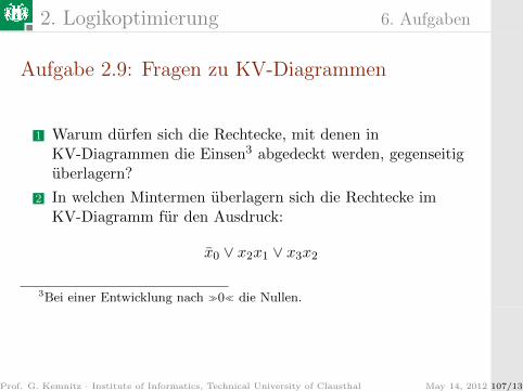
Aufgabe 2.9: Fragen zu KV-Diagrammen
1 Warum durfen sich die Rechtecke, mit denen inKV-Diagrammen die Einsen3 abgedeckt werden, gegenseitiguberlagern?
2 In welchen Mintermen uberlagern sich die Rechtecke imKV-Diagramm fur den Ausdruck:
x0 ∨ x2x1 ∨ x3x2
3Bei einer Entwicklung nach �0� die Nullen.
Prof. G. Kemnitz · Institute of Informatics, Technical University of Clausthal May 14, 2012 107/135
2. Logikoptimierung 6. Aufgaben
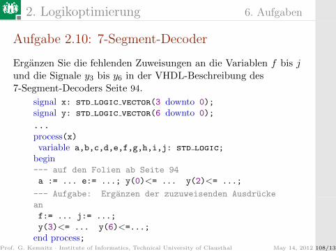
Aufgabe 2.10: 7-Segment-Decoder
Erganzen Sie die fehlenden Zuweisungen an die Variablen f bis jund die Signale y3 bis y6 in der VHDL-Beschreibung des7-Segment-Decoders Seite 94.
signal x: std logic vector(3 downto 0);
signal y: std logic vector(6 downto 0);
...process(x)variable a,b,c,d,e,f,g,h,i,j: std logic;
begin--- auf den Folien ab Seite 94
a := ... e:= ...; y(0)<= ... y(2)<= ...;
--- Aufgabe: Erganzen der zuzuweisenden Ausdrucke
an
f:= ... j:= ...;
y(3)<= ... y(6)<=...;end process;
Prof. G. Kemnitz · Institute of Informatics, Technical University of Clausthal May 14, 2012 108/135

2. Logikoptimierung 6. Aufgaben
x
y
x0
x0
x1
x1
x2 x2 x2 x2
x3
x3x3x3
y0
y2y4
y6
y3
y1y5 0000 0001 0010 0011 0100 0101 0110 0111 1000 1001
belie-
sonst
big
0
01
1
11
1 1
1
1-
-
-
-
-
-
0
0
0
1
1
1
11
1
1
-
-
-
-
-
-0
1
1
1 1
1
1 1
1
1
-
-
-
-
-
-
1
1
1
1
1
1 1
10
0
-
-
-
-
-
-
0
0
01
1 1
1
1 1
1
-
-
-
-
-
-
. . .
1
10
0 0
00
-
-
-
-
-
-
1
0
1
0
0
0 0
1 1
1
1
1
1-
-
-
-
-
-
y0 y1 y2 y3
y4 y5 y6
a := x3x2x1x0
b := x2x1x0
c := x2x1x0
d := x2x1x0
e := x2x1x0
a
b
a
b
f
e
c
d
j
f
b
a
h
ig
Prof. G. Kemnitz · Institute of Informatics, Technical University of Clausthal May 14, 2012 109/135
2. Logikoptimierung 6. Aufgaben
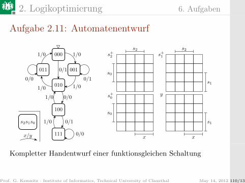
Aufgabe 2.11: Automatenentwurf
s0
s1
s2
s0
s1
s2
x x
s2s1s0
x/y
0/0
000
010
100
111
011 001
1/0 1/0
1/0
0/10/0
1/0
1/0
1/0 0/1
0/0
0/1
s+0y
s+2 s+1
Kompletter Handentwurf einer funktionsgleichen Schaltung
Prof. G. Kemnitz · Institute of Informatics, Technical University of Clausthal May 14, 2012 110/135
2. Logikoptimierung 6. Aufgaben
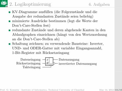
KV-Diagramme ausfullen (die Folgezustande und dieAusgabe der redundanten Zustande seien beliebig)minimierte Ausdrucke bestimmen (legt die Werte derDon’t-Care-Stellen fest)redundante Zustande und deren abgehende Kanten in denAblaufgraphen einzeichnen (hangt von den Wertzuordnungan die Don’t-Care-Stellen ab)Schaltung zeichnen; zu verwendende Bausteine: Inverter,UND- und ODER-Gatter mit variabler Eingangsanzahl,1-Bit-Register mit Rucksetzeingang
xR
Datenausganginvertierter Datenausgang
DateneingangRucksetzeingang
Takteingang
Prof. G. Kemnitz · Institute of Informatics, Technical University of Clausthal May 14, 2012 111/135

2. Logikoptimierung 6. Aufgaben
Aufgabe 2.12: Schaltungsminimierung nach Quineund McCluskey
Gegeben ist die Menge Minterme, fur die der Funktionswert�1� ist:
K ∈ {100000, 100100, 101010, 101110, 111110, 110000,
011000, 101011, 101111, 101000, 101001}
Aufstellen der quineschen Tabellen
Aufstellen der Tabelle der Primterme
Suche der minimalen Abdeckungsmenge
Prof. G. Kemnitz · Institute of Informatics, Technical University of Clausthal May 14, 2012 112/135

3. BDD
BDD
Prof. G. Kemnitz · Institute of Informatics, Technical University of Clausthal May 14, 2012 113/135

3. BDD
Binares Entscheidungsdiagramm
(BDD – binary decision diagram)
Zusammensetzung einer Funktion aus binarenEntscheidungenRekursive Definition: Eine binare Entscheidung ist eineKonstante oder eine Entscheidung zwischen binarenEntscheidungen
0 110
Entscheidung anhandeiner binaren Variablen
binare Entscheidung
Konstante
xi
Prof. G. Kemnitz · Institute of Informatics, Technical University of Clausthal May 14, 2012 114/135

3. BDD
Wertetabelle als binares Entscheidungsdiagramm
0
0
1
1 10
0 1 1 0
0110
0 00 1
011 1
yx1 x0 x0
x1 x1
Prof. G. Kemnitz · Institute of Informatics, Technical University of Clausthal May 14, 2012 115/135

3. BDD
Binaren Entscheidungsdiagramm als Programm
0
0
1
1 10
0 1 1 0
x0
x1 x1
if x0=’0’ then
if x1=’0’ then
y<=’0’;else
y<=’1’;end if;
else
if x1=’0’ then
y<=’1’;else
y<=’0’;end if;
end if;
Prof. G. Kemnitz · Institute of Informatics, Technical University of Clausthal May 14, 2012 116/135

3. BDD 1. Vereinfachungsregeln
Vereinfachungsregeln
Prof. G. Kemnitz · Institute of Informatics, Technical University of Clausthal May 14, 2012 117/135

3. BDD 1. Vereinfachungsregeln
Unreduziertes binares Entscheidungsdiagramm
Abkurzung: BDD (binary decision diagram)
0 0
0 1 0 1 0 1 0 1
11
0 1
1 0 0 1 0 1 1 0
x0
x1
x2 x2
x2
x1x1
Baumdirekt ablesbar aus der Wertetabelle
Prof. G. Kemnitz · Institute of Informatics, Technical University of Clausthal May 14, 2012 118/135

3. BDD 1. Vereinfachungsregeln
Vereinfachungsregeln
Verschmelzung gleicher TeilgraphenLoschen von Knoten mit zwei gleichen Nachfolgern
0 1100 11 0
Knoten-elimination
10
xjxi
≡
xi xj
Verschmelzung gleicher Teilbaume
xi
Offensichtliche Optimierungsvoraussetzung: gleicheAbfragereihenfolge auf allen Entscheidungswegen
Prof. G. Kemnitz · Institute of Informatics, Technical University of Clausthal May 14, 2012 119/135

3. BDD 1. Vereinfachungsregeln
Geordnetes binares Entscheidungsdiagramm
Gleiche Abfragereihenfolge auf allen Entscheidungswegen.Abkurzung:
OBDD (ordered binary decision diagram)
0 0
0 1 0 1 0 1 0 1
11
0 1
1 0 0 1 0 1 1 0
x0
x1 x1
x2 x2 x2 x2
Bezeichnung fur ein vereinfachtes binares Entscheidungsdiagr.:
ROBDD (reduced ordered binary decision diagram)
Prof. G. Kemnitz · Institute of Informatics, Technical University of Clausthal May 14, 2012 120/135
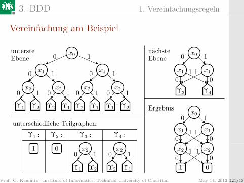
3. BDD 1. Vereinfachungsregeln
Vereinfachung am Beispiel
0 1
0 1
0 1 0 1
0
0 1 0 1
1
Υ2Υ2Υ2
0 1
0
0
10
01
1
1
10
01
0 1 0 1
Υ2 Υ2
10
1
01
Υ1 Υ1 Υ1Υ1
0Υ1 Υ1
unterste
unterschiedliche Teilgraphen:
Υ2
nachste
Ergebnis
EbeneEbene
Υ3 :Υ1 : Υ2 : Υ4 :
x0
x1 x1
x2 x2 x2 x2
x2 x2
x0
x1 x1
x0
x1 x1
x2 x2
Υ3 Υ4
Prof. G. Kemnitz · Institute of Informatics, Technical University of Clausthal May 14, 2012 121/135

3. BDD 2. Operationen mit ROBDDs
Operationen mit ROBDDs
Prof. G. Kemnitz · Institute of Informatics, Technical University of Clausthal May 14, 2012 122/135

3. BDD 2. Operationen mit ROBDDs
Zweistellige Operationen mit ROBDD
fur zwei beliebige Teilbaume, bei denen im obersten Knotendieselbe Variable ausgewertet wird, verschiebt sich dieOperation eine Entscheidungsebene tiefer
1010 0 1
Υ3 Υ4Υ2Υ1Υ4Υ1 Υ2
xixixi
beliebige zweistellige binare Operation
Υ3
⋄⋄ ⋄
⋄
in einem ROBDD erfolgen auf allen Wegen dieEntscheidungen in derselben Reihenfolge
Prof. G. Kemnitz · Institute of Informatics, Technical University of Clausthal May 14, 2012 123/135
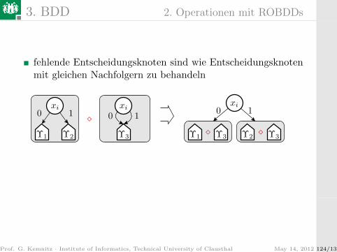
3. BDD 2. Operationen mit ROBDDs
fehlende Entscheidungsknoten sind wie Entscheidungsknotenmit gleichen Nachfolgern zu behandeln
10 100 1
Υ3 Υ3Υ1 Υ2
xi
Υ1Υ3 Υ2
xixi
⋄⋄ ⋄
Prof. G. Kemnitz · Institute of Informatics, Technical University of Clausthal May 14, 2012 124/135

0 1
0 1
0 1
0 1
0 1 0 1
0 10
0
11
0 1 0 1
0 1
0 1
00 1 0 11 10
0 1
10
0 1 0 1
0 1
0 1 1 1
0 1
x0
x0 x1
x1 x1
x0
x1 x1
x0
x1 x1
x0
x1
dungsebenen tieferOperation zwei Entschei-
dungsebene tieferOperation ein Entschei-
∨
ODER-Verknupfungx1 ∨ x0
Ausfuhrung der
Vereinfachung
Operation auf deruntersten Ebene
∨ ∨ ∨ ∨
∨∨

0 1
0 1
0 1
0
11
1
10
0
0
0 1 0 1
101
0
0 1
0 1
0
1
0 1
0
0
1
10 1
00 0 11 01 1 0 1
0 0 1 0
10
1 01 0 0
0 11 0
x3
x2
x3
x1
x2
x1
x3
x2
x1
x3 x3
x3
x2
x1
x3
x2
x1
x3
dungsebenen tieferOperation zwei Entschei-
∧
Verknupfung(x1 ∨ x2) ∧ x3
Ausfuhrung derOperation auf deruntersten Ebene
∧ ∧ ∧ ∧
dungsebenen tieferOperation drei Entschei-
Vereinfachung
∧∧

3. BDD 3. ROBDD ⇒ minimierte Schaltung
ROBDD ⇒ minimierte Schaltung
Prof. G. Kemnitz · Institute of Informatics, Technical University of Clausthal May 14, 2012 127/135

3. BDD 3. ROBDD ⇒ minimierte Schaltung
Entscheidungsknoten als Signalflussumschalter
Entscheidungsknoten ⇒ binarer Umschalter im Datenfluss(Multiplexer); 3-stellige logische Funktion
0 1
x2
x1
s
0
0 0 1
11 0
1 y = x1s ∨ x2s
01
s
x2
x1
s
x1 x2
y
y
b
a
a: x1sb: x2s
minimiert mit einem KV-Diagramm:
y = x1s ∨ x2s
Prof. G. Kemnitz · Institute of Informatics, Technical University of Clausthal May 14, 2012 128/135

3. BDD 3. ROBDD ⇒ minimierte Schaltung
eine konstante Eingabe ⇒ 2-stellige logische Funktion
x1 = 0 : y = (0 ∧ s) ∨ x2s = x2s
x1 = 1 : y = (1 ∧ s) ∨ x2s = s ∨ x2s = s ∨ x2
x2 = 0 : y = x1s ∨ (0 ∧ s) = x1s
x2 = 1 : y = x1s ∨ (1 ∧ s) = x1s ∨ s = x1 ∨ s
zwei konstante Eingaben ⇒ 1-stellige logische Funktion
x1 = 0; x2 = 1 : y = (0 ∧ s) ∨ (1 ∧ s) = s
x1 = 1; x2 = 0 : y = (1 ∧ s) ∨ (0 ∧ s) = s
&
y
ys
x2
01
s
x2
0
≥1
y
ys
x1
01
s
1
x1
ys
y01
s
0
1y
01
s
s y
0
1
· · ·
Prof. G. Kemnitz · Institute of Informatics, Technical University of Clausthal May 14, 2012 129/135
3. BDD 3. ROBDD ⇒ minimierte Schaltung
Entscheidungsdiagramm als Signalflussplan
0
0
10
01
1
1
10
0 1
x1
x0
x2
x1
x2
(k2)
(k1)
(k4)
(k3)
(k5)
y
(k2)
(k1)
(k3)
x1
x0
(k4)
(k5)
01
01
01
x2
x2
Prof. G. Kemnitz · Institute of Informatics, Technical University of Clausthal May 14, 2012 130/135

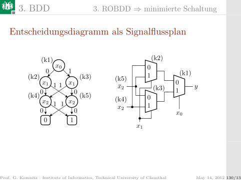
3. BDD 3. ROBDD ⇒ minimierte Schaltung
Abfragereihenfolge und Schaltungsaufwand
Zielfunktion: y = (x1 ∨ x0) ∧ x2
1
1
10
0
0 10
01
0 1
0 1 0 1
&&&
&
y
0 1
Abfragereihenfolge: x0-x1-x2
y
≥1
Abfragereihenfolge: x2-x1-x0
x1
y
x0
x1
x2
x0
x1
x2
x0
x1 x2
x2
x1
x0 x0
&
≥1x2
Abfragereihenfolge x0 − x1 − x2: 1 Multiplexer, 1 UND, 1InverterAbfragereihenfolge x2−x1−x0: 1 ODER, 1 UND, 1 Inverter
Prof. G. Kemnitz · Institute of Informatics, Technical University of Clausthal May 14, 2012 131/135

3. BDD 3. ROBDD ⇒ minimierte Schaltung
ein ROBDD mit einer vorgegebenen Abfragereihenfolge isteine eindeutige Darstellung fur eine logische Funktion
eine n-stellige logische Funktion lasst sich (nur) durch(n− 1)! verschiedene ROBDDs darstellen (mit Ausdruckenist die Anzahl der Darstellungsmoglichkeiten unbegrenzt)
Losungsraum nicht auf UND-ODER-/ODER-UND-Strukturbeschrankt
Optimierung durch Variation der Abfragereihenfolge; oftgute Optimierungsergebnisse
Ausnutzung der Eindeutigkeit der Darstellung fur den Testauf Gleichheit von logischen Funktionen, z.B. einer Ist- undeiner Soll-Funktion, ohne die Schaltungen mit allenEingabevariationen simulieren zu mussen
Prof. G. Kemnitz · Institute of Informatics, Technical University of Clausthal May 14, 2012 132/135

3. BDD 4. Aufgaben
Aufgaben
Prof. G. Kemnitz · Institute of Informatics, Technical University of Clausthal May 14, 2012 133/135
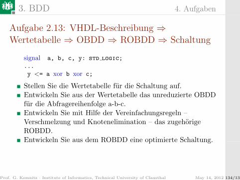
3. BDD 4. Aufgaben
Aufgabe 2.13: VHDL-Beschreibung ⇒Wertetabelle ⇒ OBDD ⇒ ROBDD ⇒ Schaltung
signal a, b, c, y: std logic;
...
y <= a xor b xor c;
Stellen Sie die Wertetabelle fur die Schaltung auf.Entwickeln Sie aus der Wertetabelle das unreduzierte OBDDfur die Abfragereihenfolge a-b-c.Entwickeln Sie mit Hilfe der Vereinfachungsregeln –Verschmelzung und Knotenelimination – das zugehorigeROBDD.Entwickeln Sie aus dem ROBDD eine optimierte Schaltung.
Prof. G. Kemnitz · Institute of Informatics, Technical University of Clausthal May 14, 2012 134/135

3. BDD 4. Aufgaben
Aufgabe 2.14: ROBDD⇒Wertetabelle, Schaltung
0
0
1
10
1
10
x0
x1
x2
Stellen Sie die Wertetabelle auf.
Bilden Sie das Entscheidungsdiagramm durch einenDatenflussplan nach.
Prof. G. Kemnitz · Institute of Informatics, Technical University of Clausthal May 14, 2012 135/135