design of low voltage improved performance current mirror
TRANSCRIPT
Control Theory and Informatics www.iiste.org
ISSN 2224-5774 (Paper) ISSN 2225-0492 (Online)
Vol.4, No.2, 2014
26
Design of Low Voltage Improved performance Current Mirror Nidhi Tarun, Shruti Suman, P. K. Ghosh
ECE Department
Faculty of Engineering and Technology
Mody University of Science & Technology
Lakshmangarh, Sikar, Rajasthan, India
Abstract
This paper proposes a low voltage current mirror circuit with low input impedance and high output impedance. These improvements are obtained by adding an amplifier which provides biasing voltage to the transistors. Its operation and results are compared with conventional and cascode current mirror circuits. The circuits are designed using Tanner EDA Tool in 90nm CMOS technology with 0.8V supply voltage. Simulation results shows that the minimum output voltage is reduced to 0.1 V, also input resistance is reduced to 0.179kΩ and consumes only 46µW power.
Keywords: Current mirror, Input resistance Output resistance, Input compliance voltage, Output compliance voltage.
1. Introduction
In analog circuit design, current mirror is used as a fundamental building block for a large number of integrated circuits like OTAs (operational trans-conductance amplifiers), Current Conveyors, CFOAs (current feedback operational amplifiers), filters etc [S. Chatterjee, Y. Tsividis, and P. Kinget (2005)]. Efficiency of a Current Mirror has had a direct impact on the overall performance of these integrated circuits. Relevant performance parameters of current mirrors in these applications include linearity in current transfer, power consumption, minimum supply voltage, input and output resistances [Paul R Gray, Paul J Hurst, Stephen H Lewis and Robert G. Meyer, A. S., Smith, K. C. (2005)]. One of the major drawbacks in conventional current mirror is their high input impedance and low output impedance. Many literatures have studied the problems of input impedance [S. C. Terry, M. M. Mojarradi, B. J. Blalock, and J. A. Richmond (2005), B. Aggarwal, and M. Gupta (2009), X.-G. Zhang and E. I. El-Masry (2004)]. Further a voltage amplifier is inserted between the drain and gate of input transistor to decrease the input impedance and also several possible implementations of the amplifier are studied. However these configurations suffer from poor stability problem. The better performance is achieved in case of using a differential amplifier [Nairn, D. G, Salama (1990)]. However drawback of differential amplifier is that it requires high supply voltage and more power consumption. The active input regulated cascode (AIRC) is further introduced with differential amplifiers in both input and output sides of current mirror and the circuit is claimed to have very low input and high output resistances [Serrano, T., Linares Barranco, B. (1994)]. Further, a current mirror is proposed which achieves low input impedance using flipped voltage follower (FVF) scheme. This scheme has some disadvantages of transient and bandwidth performance degradation, circuit complexity, and higher power consumption. Also it requires careful design of biasing network [Carvajal, R., Ramirez-Angulo, J., Lopez Martin, A., Torralba.A (2005)]. Current Mirrors based on alternative architectures such as bulk-driven, floating-gate, subthreshold etc are also presented. Bulk-driven based Current Mirror suffers from a lot of parasitics and reduced swing. In sub threshold current mirrors, the trans-conductance of the mirroring transistors is very low and hence their bandwidth is very poor also the current matching accuracy of these mirrors is also very low [Ramirez Angulo, J.Sawant, M.S. Lopez Martin, A., & Carvajal, R. G. Compact (2005), Naresh Lakkamraju, Ashish Kumar Mal (2011), Bradley A. Minch (2012)].
A current mirror is proposed which has low voltage, low input and high output impedances. The principle of operation of proposed current mirror is compared with simple current mirror. One of the major drawbacks of the conventional current mirrors is rather high input impedance, while especially in current mode signal processing the node impedances have to be very small. In fact this impedance has a substantial effect on overall dynamic range and frequency response of the circuit.
2. Conventional Current Mirror
A conventional Current Mirror structure (Figure 1) uses M1 in diode-connected configuration and the input

Control Theory and Informatics www.iiste.org
ISSN 2224-5774 (Paper) ISSN 2225-0492 (Online)
Vol.4, No.2, 2014
27
voltage inV is required to pump input current inI into the input port of the mirror. As evident, inV depends solely on the biasing conditions of M1, which operates in saturation. Its trans-conductance 1mg decides the input impedance inR of the Current Mirror.
For Conventional current mirror, input compliance voltage inV is given by
iIVV intin β/2+= (1)
where,
tV is the threshold voltage , iβ = L
WCOXµ , µ is the carrier mobility, OXC is oxide capacitance. W and L
refer to the width and length of the MOS transistors. The input current inI is given as
2
1
1 )( tGSoxin VVL
WCI −= µ (2)
From Figure 1, transistor M1 operating in saturation region which drives transistor M2 also in saturation and MOS transistor works as a constant current source. From equation (1) the lower limit of input voltage inV of conventional current mirror is restricted to at least the value of the threshold voltagetV . If the input current inI is too low, this drives transistor M1 into sub-threshold region. The desired characteristics for current mirror circuit are to work under sub threshold operation, its input voltage refin VV = is sufficiently low (≤100 mV). To force M1 and M2 into sub-threshold region, one needs to increase the aspect ratios
L
Wof these transistors
which in turn lower the value of input voltageinV . But circuits based on sub-threshold have poor frequency response and these circuits cannot be used in high frequency applications.
The output compliance voltage outV required for Conventional Current Mirror is given by
)(satDSout VV = (3)
where,
)(satDSV is drain to source saturated voltage.
The conventional current mirror suffers two major drawbacks; it requires an input compliance voltage which is always greater than a threshold voltage tV and its output impedance is low. So this structure cannot provide requisite gains. One practice is to increase the output impedance of such a structure is to use cascode structure at the output port. The cascode Current Mirror of Figure 2 is the example of enhanced output impedance current mirror [P.E. Allen and D.R. Holberg, Holt, Rinehart and Winston(1987), R.L. Geiger, P.E. Allen, and N.R. Strader, D.A. Johns, K. Martin(1990), S.S. Rajput and S.S. Jamuar(2002)].
The input compliance voltage of cascode current mirror is given as
iintin IVV β/222 += (4)
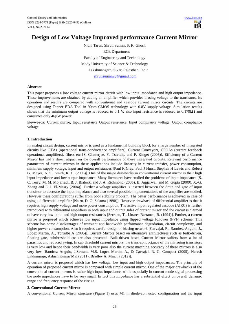
Input voltage of cascode current mirror is double of the input compliance voltage obtained with conventional current mirror of Figure 1. Hence, for low voltage applications, cascade current mirror shown in Figure 2 is not suitable and the analogue designers prefer single transistor at the input port while keeping the cascode structure at the output port as shown in Figure 3. Problem with this circuit is to provide suitable biasing voltage )( bV for charging the gate of M3.
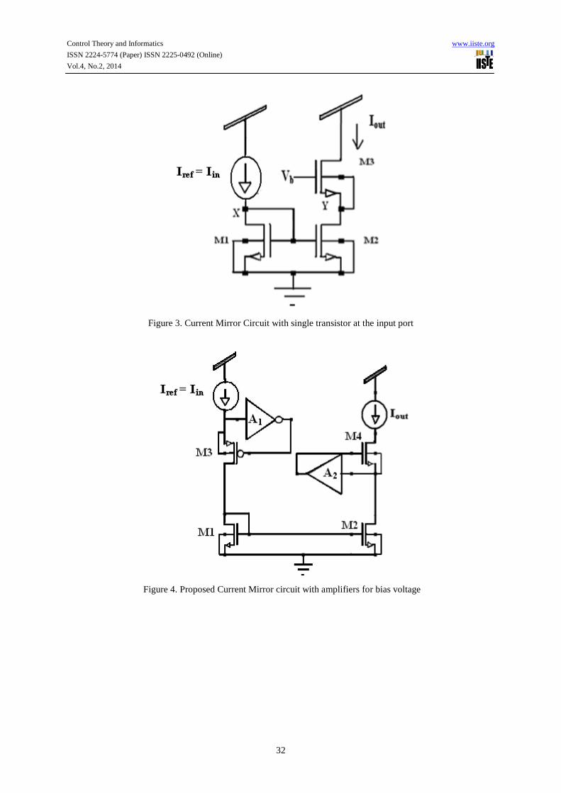
3. Proposed Current Mirror
In order to provide suitable biasing amplifiers of gain A1 and A2 are inserted in the proposed design which provides suitable biasing voltage to turn on transistor M3 and M4 respectively and provides high gain when working in saturation, as shown in Figure 4. Once transistor M4 is turned on, same output resistance as in cascode current mirror is observed. To obtain low input impedance, we incorporate transistor M3 in series with the input terminal of the basic circuit of the current mirror and use an amplifier of gain ‘-A1’ to control the gate voltage of transistor M3, Amplifier of gain A2. Any increment in source voltage of transistor M3 (because of injected input current) causes its gate voltage to decrease ‘-A1’ times this works as stronger sink of input current which results in input impedance decrement by ‘A1’.
Figure 5 shows transistor level implementations of this idea which shows the amplifier can be implemented by only two transistors which act as a simple inverter for which input voltage is obtained as:

Control Theory and Informatics www.iiste.org
ISSN 2224-5774 (Paper) ISSN 2225-0492 (Online)
Vol.4, No.2, 2014
28
53 dssgin VVV += (5)
For the amplifier to have the significant gain required for perfect operation of the circuit, transistors M5 and M6 should operate in saturation region. If either of M5 or M6 is not in saturation condition, amplifier gain reduces and finally leading to increase in input impedance.
3.1 Input Resistance Analysis
Figure 6 shows the small signal equivalent circuit for the proposed circuit in which the direction of p-type current mirrors are drawn opposite to the direction of n-type. From Figure 7 we get,
insggs VVV == 65 (6)
054 == ss VV (7)
))(( 6566553 dsdsgsmgsmgs rrVgVgV +−= (8)
indsdsmmgs VrrggV ))(( 65653 += (9)
With reference to the basic proposed circuit of Figure 4, the voltage gain A1 is defined as
in
gs
V
VA 3
1 −= (10)
Using equation (6) to (9), this simplifies to
))(( 15651 dsdsmm rrggA += )/()( 6565 dsdsmm gggg ++= (11)
33311
)(1
dsingsmdsm
inin rIVgrg
IV ++
= (12)
3331
)(1
dsingsmm
in rIVgg
I ++
≅ (13)
inSggs VAVVV )1( 1333 +−=−= (14)
31331
)1(1
dsinindsmm
inin rIVArgg
IV ++−
= (15)
+=+ 3
1133
1)1( ds
mindsmin r
gIArgV (16)
The input impedance inR then obtained as
)1(1)1(1
1
133
3
133
31
++≅
++
+
==Arg
r
Arg
rg
I
VR
dsm
ds
dsm
dsm
in
inin (17)
From analysis it is clearly observed that the input resistance of proposed current mirror circuit depends on the amplification gain A1. Higher the amplification gain, the lower will be the input resistance and in order to achieve higher gain, it is necessary that both transistor M7 and M8 (PMOS and NMOS) should work in saturation region.
3.2 Output Resistance Analysis
The small signal circuit for calculating the output resistance of proposed current mirror is given in Figure 7. Applying KCL at the output node in Figure 7 we get-
)( 4444 sodsgsmuto VVrVgI −+= (18)
444444 )( sdsodssgmout VrVrVVgI −+−= (19)
442 / sg VVA = (20)
42 Sgs VAV = (21)

Control Theory and Informatics www.iiste.org
ISSN 2224-5774 (Paper) ISSN 2225-0492 (Online)
Vol.4, No.2, 2014
29
444244 )1( sdsodsgsmout VrVrAVgI −+−= (22)
24 dsouts rIV = (23)
Putting all the values, we get
442244 ))1(1( dsodsdsdsmout rVrrArgI =+−+ (24)
The output impedance oR is given as
)1(/ 42224 dsdsdsmoutoo rrArgIVR ++== (25)
2424 ArrgR dsdsmo = (26)
Output resistance of proposed mirror circuit is equivalent to cascode current mirror and also it depends on amplification gain A2. Higher the amplification gain of amplifier, more will be its output resistance.
4. Simulation Results for existing current mirrors
Simulations are carried on Tanner EDA Tool on 90nm CMOS technology utilizing 1 V power supply. Input characteristic, output characteristic and frequency response of existing current mirror are simulated. The bias current is taken as 50 µA on which the ac input current is superimposed.
4.1 Input characteristic of Conventional and Cascode current mirror
Figure 8 shows the input characteristic of conventional current mirror circuit which shows a variation of input current from 0 to 1.5 mA over the input voltage varying from 0 to 1.0 volts. Because of single transistor at the input side in conventional current mirror, it shows minimum input compilance voltage of 0.4 V. For a companion, the input characteristic of cascode current mirror circuit is shown in figure 9. A notable change in input characteristic of cascode current mirror is obtained due to reduced resistance. The minimum input compilance voltage in this case is 0.6V.
4.2 Output characteristic of Conventional and Cascode current mirror circuit
In VLSI design, output resistance of current mirror should high so that proper matching between circuits will take place. Ideally it should be infinite but practically its value is limited. Figures 10 and 11 shows the output characteristics of conventional current mirror and cascode current mirror, respectively. Cascode current mirror shows better results because of cascoding (one transistor over another). The reduction in output current of Figure 11 as compared to Figure 10 is an indication that the output resistance of cascode current mirror is high.
4.3. Frequency response of Conventional and Cascode Current Mirror circuit
The bandwidth of operation of conventional current mirror is wider than that of cascode current mirror, as evident from the frequency response characteristic of circuits shown in Figure 12 for conventional and Figure 13 for cascode current mirrors. Formation of series capacitance increases the bandwidth in conventional current mirror while in cascode current mirror, there is parasitic capacitance in parallel which degrade its frequency response.
5. Simulation Results for proposed current mirror
5.1 Input characteristic of proposed Current Mirror circuit
It is desirable for low voltage operation that M1 and M2 operate either in sub-threshold or in saturation region. PMOS transistor is added in series with NMOS transistor which works as a current source. By applying proper biasing voltage, the turn on condition of PMOS transistor will ensure NMOS transistor to work in saturation region. Also when M7 and M8 enter into saturation region, this in turn, lowers the input resistance. The minimum input voltage of proposed current mirror is obtained as 0.3V. Figure 14 shows the input characteristic of proposed current mirror.
5.2 Output characteristic of Proposed Current Mirror circuit
The minimum output voltage of the proposed current mirror is reduced to 0.1V as observed from Figure 15. Also high swing at output is obtained. Reduction in )min(outV is because of cascoding of transistors.
5.3 Frequency response of proposed Current Mirror circuit
The current through M4 should be small enough to keep M4 in sub-threshold region. Correspondingly W/L ratio should also be large. This will increase the device capacitance and bandwidth. Figure 16 shows a frequency response of proposed current mirror. From this figure a bandwidth of 98.45 MHz is obtained.

Control Theory and Informatics www.iiste.org
ISSN 2224-5774 (Paper) ISSN 2225-0492 (Online)
Vol.4, No.2, 2014
30
6. Conclusion
A novel structure to improve conventional current mirror’s input impedance and output impedance is introduced. The principle of the input impedance reduction and increment of output impedance is discussed. A comparison between the features of the proposed current mirror and the basic and cascode current mirrors is presented both in analytic and simulation format. It is shown that input impedance is reduced and output impedance is increased significantly as compared to that of the simple current mirror. Simulations are carried on Tanner EDA Tool on 90nm CMOS technology are presented to demonstrate the performance validation of the proposed current mirror. As is shown the proposed current mirror achieves low input impedances and high output impedance without degrading other specifications.
References
S. Chatterjee, Y. Tsividis, and P. Kinget , "0.5-V analog circuit techniques and their application in OTA and filter design," IEEE Journal of Solid-State Circuits, vol.40, no.12, pp. 2373- 2387, December, 2005. Paul R Gray, Paul J Hurst, Stephen H Lewis and Robert G Meyer (1984) ,“Analysis and design of Analog Integrated Circuits” by John Wiley & sons.
Sedra, A. S., and Smith, K. C. Microelectronics circuits (5th ed . 2005).. New York: Oxford University Press.
S. C. Terry, M. M. Mojarradi, B. J. Blalock, and J. A. Richmond, “Adaptive gate biasing: a new solution for body-driven current mirrors”, ACM Great Lakes Symposium on VLSI, pp.472~477, April, 2005. B. Aggarwal, and M. Gupta, “Low-voltage cascode current mirror based on bulk-driven MOSFET and FGMOS techniques,” Intternational Conference on Advances in Recent Technologies in Communication and Computing, pp. 473-477, October, 2009. X.-G. Zhang, and E. I. El-Masry, "A regulated body-driven CMOS current mirror for low-voltage applications," IEEE Transactions on Circuits and Systems II: Express Briefs , vol.51, no.10, pp. 571- 577, October, 2004. Nairn, D. G., and Salama, C. A. T. (1990). Current mode algorithmic analog to digital converters. IEEE Journal of Solid State Circuits, 25, 997–1004.
Yuan, F., and Sun, B. (2002). A comparative study of low-voltage CMOS current-mode circuits for optical communications. In Circuits and systems, 45th midwest symposium on IEEE (Vol. 1, pp. I-315–I-319).
Serrano, T., and Linares-Barranco, B. (1994). The active input regulated cascode current mirror. IEEE Transactions on Circuits and Systems-I: Fundamental Theory and Application, 41(6), 464–467.
Carvajal, R., Ramirez-Angulo, J., Lopez Martin, A., Torralba, A., Galan, J., Carlosena, A., et al. (2005).
The flipped voltage follower A useful cell for low voltage low power circuit design. IEEE Transactions on Circuits and Systems.
Ramirez Angulo, J, Carvajal. R. G. and Torralba.A. (2004). Low supply voltage high-performance CMOS current mirror with low input and output voltage requirements. IEEE Transactions on Circuits and Systems-II.
Ramirez-Angulo, J. Sawant, M. S. Lopez Martin and Carvajal (2005). “ Compact implementation of high performance CMOS current mirror”. Electronics Letters.
Naresh Lakkamraju, Ashish Kumar Mal “Low Voltage High Output Impedance Bulk Driven Regulated Cascode Current Mirror” IEEE- 2011.
Bradley A. Minch,” Low-Voltage Cascode Current Mirror with Enhanced Dynamic Performance” IEEE Trans. Circ. Syst. II, Oct. 2012.
P.E. Allen and D.R. Holberg, CMOS Analog Circuit Design, Holt, Rinehart and Winston, Inc. New York, 1987.
R.L. Geiger, P.E. Allen, and N.R. Strader VLSI Design Techniques for Analog and Digital Circuits. Mc-Graw Hill: New York, 1990.
D.A. Johns and K. Martin, Analog Integrated Circuit Design. John Wiley & Sons, Inc., New York, 1997.
S.S. Rajput and S.S. Jamuar, “Current mirrors Essential units for analog circuit structures.” IETE 2002.
Ms. Nidhi Tarun is pursuing M.Tech. from Mody University of Science and Technology, Lakshmangarh, Sikar, Rajasthan, India. She has completed her B. Tech. from Rajasthan Technical university, India, in the year 2010.

Control Theory and Informatics www.iiste.org
ISSN 2224-5774 (Paper) ISSN 2225-0492 (Online)
Vol.4, No.2, 2014
31
Her Research Interests are in the field of VLSI Design.
Ms. Shruti Suman did M.Tech. from Mody Institute of Technology and Science Lakshmangarh, Sikar, Rajasthan, India in the year 2012. She has completed B.E. from Rajeev Gandhi Technical University, Bhopal, India, in the year 2010. She is working as Assistant Professor in ECE Department, Mody University of Science and Technology, Lakshmangarh, Sikar, Rajasthan (India).Her Research Interests are in Analog and Digital VLSI Design. She has over 7 papers to her credits in International Journals /Conferences including IEEE.
Dr. P. K. Ghosh was born in Kolkata, India in 1964. He received his B.Sc (Hons in Physics), B.Tech and M.Tech degrees in 1986, 1989, and 1991, respectively from Calcutta University. He earned Ph.D. (Tech) degree in Radio Physics and Electronics in 1997 from the same University. He served various institutions, namely, National Institute of Science and Technology (Orissa), St. Xavier’s College (Kolkata), Murshidabad College of Engineering and Technology (West Bengal), R. D. Engineering College (Uttar Pradesh) and Kalyani Government Engineering College (West Bengal) before he joined Mody University of Science and Technology (Rajasthan). To his credit, he has more than 50 research papers in Journals of repute and conference proceedings. He is life member of Indian Society for Technical Education (ISTE), New Delhi. His research interests are in the areas of VLSI circuits & devices, wireless communications and signal processing.
Figure 1. Conventional Current Mirror circuit
Figure 2. Cascode Current Mirror circuit
Control Theory and Informatics www.iiste.org
ISSN 2224-5774 (Paper) ISSN 2225-0492 (Online)
Vol.4, No.2, 2014
32
Figure 3. Current Mirror Circuit with single transistor at the input port
Figure 4. Proposed Current Mirror circuit with amplifiers for bias voltage

Control Theory and Informatics www.iiste.org
ISSN 2224-5774 (Paper) ISSN 2225-0492 (Online)
Vol.4, No.2, 2014
33
Figure 5. Transistor level implementation of Proposed Current Mirror circuit
Figure 6. Small signal analysis of proposed circuit for calculating input resistance

Control Theory and Informatics www.iiste.org
ISSN 2224-5774 (Paper) ISSN 2225-0492 (Online)
Vol.4, No.2, 2014
34
Figure 7. Small signal analysis of proposed circuit for calculating output resistance
Figure 8. Input characteristic of Conventional Current Mirror circuit

Control Theory and Informatics www.iiste.org
ISSN 2224-5774 (Paper) ISSN 2225-0492 (Online)
Vol.4, No.2, 2014
35
Figure 9. Input characteristic of Cascode Current Mirror circuit
Figure 10. Output characteristic of Conventional Current Mirror circuit

Control Theory and Informatics www.iiste.org
ISSN 2224-5774 (Paper) ISSN 2225-0492 (Online)
Vol.4, No.2, 2014
36
Figure 11. Output characteristic of Cascode Current Mirror circuit
Figure 12. Frequency response of Conventional Current Mirror circuit

Control Theory and Informatics www.iiste.org
ISSN 2224-5774 (Paper) ISSN 2225-0492 (Online)
Vol.4, No.2, 2014
37
Figure 13. Frequency response of Cascode Current Mirror circuit
Figure 14. Input characteristic of proposed Current Mirror circuit

Control Theory and Informatics www.iiste.org
ISSN 2224-5774 (Paper) ISSN 2225-0492 (Online)
Vol.4, No.2, 2014
38
Figure 15. Output characteristic of Proposed Current Mirror circuit
Figure 16. Frequency response of Proposed Current Mirror circuit Table1. Comparison between Conventional, Cascode and proposed Current Mirrors at 90 nm technology
Conventional Current Mirror
Cascode Current Mirror Proposed Current Mirror
Supply Voltage 1.0V 1.0V 0.8V
Minimum Input Voltage 0.4 0.6 0.3
Minimum Output Voltage 0.2 0.1 0.1 Input Resistance 0.2020KΩ 59.460KΩ 0.1790KΩ Output Resistance 125.16 KΩ 2.756MΩ 6.247MΩ
Bandwidth 876MHz 95.8 KHz 98.45MHz
Power Consumption
52.8 µW
74.186 µW
46 µW