design of microprogrammedcontrol units (mcu) using vhdl
TRANSCRIPT
1
Design of Microprogrammed Control Units (MCU) usingVHDL Description
Arvutitehnika erikusus

Arvutitehnika erikursus 2
Hardwired control unit
CLOCK
S5 A S6
D Q
¬Q
D Q
¬Q
&
A hardwired control unitaccomplishes a conditional transfer of control from step 5 to step 6 (STOP example).
This is the one-hot state assignment approach in which a separate flip-flop is dedicated to each state in the controller.

Arvutitehnika erikursus 3
Hardwired control unit
DATA PATH UNIT
CONTROL UNIT
CLOCK
S5 A S6
D Q
¬Q
D Q
¬Q
&

Arvutitehnika erikursus 4
Microprogrammed control unit
DATA PATH UNIT
CONTROL UNIT
conditions
c w-ba
a
a wCONTROLbSIGNALS
AGP
MAR MIRROM

Arvutitehnika erikursus 5
Block diagram for a MCU
conditions
c w-ba
a
a wCONTROLb
SIGNALS
AGP
MAR MIRROM
MAR - a-bit address registerROM - memory with 2a w-bit wordsMIR - w- bit instruction registerAGP - address generating logic
In a microprogrammed control unit, the values of control signals are read from an appropriate address location in a ROM (instead of being generated by combinational logic gates).The contents of each address in the ROM are called a control word.

Arvutitehnika erikursus 6
Basic microprogrammed control unit (example)
We use two-way branching address generation
Each control word contains 64 bits of dataThe condition select field (CW(63:40)) contains information needed to select the input condition signal that is used to compute the address of the next instruction.In the BMCU we use a “one-hot” code to select the condition signal
63 40 39 32 31 0
CS NAD LCS
Control WordNext Address field
If Ci is selected and Ci = 1 then address NAD field is the address of the next control word to be fetched. If Ci = 0, then the memory address [MAR] is incremented to compute the next address.

Arvutitehnika erikursus 7
Control word
63 62 61 40
CS23 CS22 CS21 . . . CS0
Condition Select Field (CS)
31 30 29 0
LCS31 LCS30 LCS29 . . . LCS0
Level Control Signal Field (LCS)
The maximum number of control signals is 32. ROM size is 256 words.
Every designer must observe the constraints imposed by the controller. These constraints include such things as the number of control signals that can be generated, the number of status signals that can be handled, and limits imposed by the address generation logic.

Arvutitehnika erikursus 8
Address generation logic
The correct sequence of control signals is obtained by generating the proper sequence of addresses at the ROM inputs.
The address generating logic varies considerably from design to design and is a major contributor to the constraints imposed by the controller.
Timing signals for the control unit and the data unit must be closely coordinated.
The controller works best if the sequencing of addresses is relatively simple. Usually, the address generating logic circuit (AG) is a counter with the option to parallel load a new address when one wishes to jump to a new point in the control sequence. If the controller usually goes to the next higher sequential address for the next set of control signal values (increment) with just an occasional need to parallel load a new address (branch), the AG can be a low complexity circuit.

Arvutitehnika erikursus 9
Address generation logic organization (example)
AS
8 8 MAR
8 next8 address
NAD
0MUX
1
INC
Address Generation Logic for BMCU can be designed using a vector multiplexer.
AS = (CW(63))(C23) + (CW(62))(C22) + … + (CW(40))(C0)
CS(23) CS(22) CS(0)

Arvutitehnika erikursus 10
Synthesis of microprogrammed controllers
1. Prepare a table showing all transitions from each state and the conditions that define each transition by scanning the statements in the VHDL description.2. Make a list of the conditions from step 1. After the assignment of ROM addresses to states, some of these conditions may not be needed.3.Identify a reset state.4. Assign a ROM address to each state.5. Remove the redundant signals from the condition list created in step2 and assign the condition signals to the condition inputs in an arbitrary manner.6. Create a list of transfers during each state and a list of outputs required during each state.7. From the list of transfers and outputs created in step 6, generate a list of control signals needed to time the transfers and outputs.8. Draw a block diagram showing the condition and control signals produced.9. Determine the ROM program using the information in the lists produced in
steps 1-8. This procedure is similar to that performed by an assembler program.

Arvutitehnika erikursus 11
Table of transitions created by executing step 1
PS NS Condition
S0 S0 R + ¬AS1` ¬R
S1 S2 ¬RS0 R
S2 S3 ¬RS0 R
S3 S4 ¬RS0 R
S4 S5 ¬RS0 R
S5 S1 ¬R & AS0 R + ¬A
Arvutitehnika erikursus 12
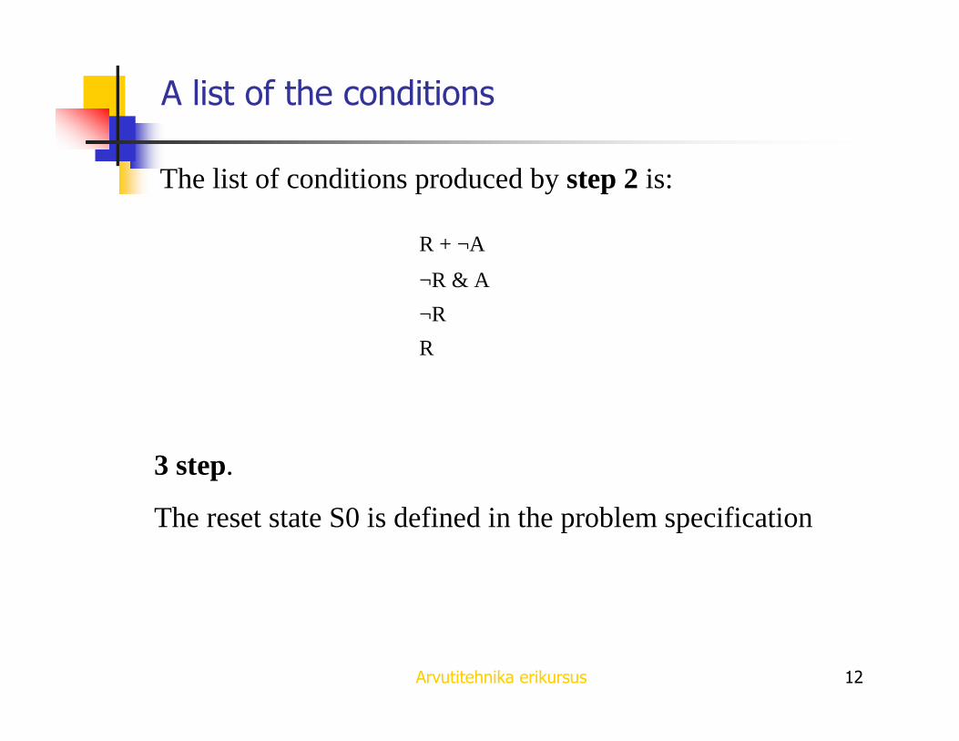
A list of the conditions
The list of conditions produced by step 2is:
R + ¬A
¬R & A
¬R
R
3 step.
The reset state S0 is defined in the problem specification

Arvutitehnika erikursus 13
Assignment of a ROM address to each state (4)
4.1. Let variable P be the current state.
Let LC represent the location counter which contains the next available memory address.
4.2. Assign state P to address LC. If all states are assigned to memory addresses, then stop.
Otherwise go to step 3.
4.3. To determine the number of ROM addresses needed to implement state P, let NSP be
the number of next states for state P.
Although the optimum assignment of addresses instep 4 is a difficult problem, the following simple approach will produce a reasonableassignment in a short time.
Programming the ROM for a controller is often accomplished using a tool similar to an assembler.

Arvutitehnika erikursus 14
The number of ROM addresses needed to P
4.3.1. If NSP=1, set LC=LC+1. Only one ROM address is needed. If the next state is not yet assigned, set P equal to the next state, mark the next state with an I (for increment), and go to step 2. If the next state is already assigned to a ROM location, then mark the next state with B (for branch), arbitrarily select any unassigned state for P, and go to step 2.
4.3.2. If NSP>1, and if all states are already assigned to ROM addresses, then NSP memory locations are required to implement state P. Mark all next states with B, set LC=LC+NSP, arbitrarily select any unassigned state for P, and go to step2.
4.3.3. If NSP>1, and if at least one of the next states of P are not assigned to a ROM address, then arbitrarily set Q equal to one of the unassigned next states of P (this is where the optimality breaks down-choice for Q). NSP-1 memory locations are required for state P. Mark Q with I, mark all other next states of P with B, set LC=LC+NSP-1, set P=Q, and go to step2.

Arvutitehnika erikursus 15
ROM address assignment
P-current state variable; LC-location counter; NSP-the number of next states for P;Q-state variable;
LC=LC+NSP-1
Q:=ArbUnasSt
Other B
P:=Q
Q mark I
All are Ass?
LC:=LC+NSP
All mark B
yes
no
I
LC:=P
NSP=1
Ass?
LC:=LC+1
B
P:=ArbUnasSt
P:=Reset LC:=0
yes
no
no yes
?!

Arvutitehnika erikursus 16
ROM address assignment (example STOP)
PS NS Condition Type
S0 S0 R + ¬A BS1` ¬R I
S1 S2 ¬R IS0 R B
S2 S3 ¬R IS0 R B
S3 S4 ¬R I
S0 R BS4 S5 ¬R I
S0 R BS5 S1 ¬R & A B
S0 R + ¬A B

Arvutitehnika erikursus 17
ROM addresses assigned to steps (Step 4)
The next available address would be address 7 because state S5 requires two memory locations.
State ROM address
S0 0S1 1
S3 3S4 4S5 5
S2 2

Arvutitehnika erikursus 18
Assignment of conditions (Step 5)
An arbitrary assignment of conditions to the condition input of the control unit:
Input Condition
C23 R
C22 R + ¬A
C21 ¬R & A
The condition signals that must be passed from the data unit to the control unit are those that correspond to lines of the table (list of transitions) that are marked with a B (branch).
Note that condition ¬R is not needed because all next states requiring condition ¬R are marked with I (increment) indicating that the transitions will be accomplished by incrementing the MAR.

Arvutitehnika erikursus 19
A list of transfers (Step 6)
State Transfer Cond Done Cond Z Cond
S0 - - 0 1 - -
S1 Shift SR 1 0 1 - -
S2 Shift SR 1 0 1 - -
S3 Shift SR 1 0 1 - -
S4 Shift SR 1 0 1 - -
S5 - - 1 1 SR 1
Note that condition 1 means an unconditional transfer or output.In this example, all transfers and outputs are unconditional.
Steps 1 and 6 are separated into two steps for clarity only.

Arvutitehnika erikursus 20
A list of control signals (Step 7)
Output Signal Transfer/Output
LCS31 SHIFT SR <= D & SR[3:1]
LCS30 DONE_CONTROL DONE = 1, Z = SR
The assignment of control signals to the output ports is arbitrary.
Since there are only two distinct output situations, the Outputs can be controlled by one control signal called DONE_CONTROL. There is only one transfer required, indicated by control signal SHIFT.

Arvutitehnika erikursus 21
Block diagram showing intermodule signals
F
F
R A D
C23DONE
…C22C21
4SHIFT
ZDONE_CONTROL
C20 C23… C22
C21C0
CONTROLUNIT
LCS31LCS30
DATAUNIT

Arvutitehnika erikursus 22
STOP block-diagram
DATA PATH UNIT
CONTROL UNIT
C21, C22, C23 2
conditions
microoperationsstatus signals
control signals
SHIFT, DONE_CONTROL
3
DONE
Z
4
RAD

Arvutitehnika erikursus 23
ROM contents for control ROM of STOP
CS NAD LCS
23 22 21 20…0 7 … 0 31 30 29…0CWORDbit 63 62 61 60…40 31 30 29…0
State Address
S0 0 0 1 0 0 … 0 0000000 0 0 ----S1 1 1 0 0 0 … 0 0000000 1 0 ----S2 2 1 0 0 0 … 0 0000000 1 0 ----S3 3 1 0 0 0 … 0 0000000 1 0 ----S4 4 1 0 0 0 … 0 0000000 1 0 ----S5 5 0 0 1 0 … 0 0000001 0 1 ----S5 6 0 1 0 0 … 0 0000000 0 1 ----
C22-the condition for branch (labeled B) operation (R + ¬A ); C21--- (¬R & A);
LCS31---SHIFT; LCS30---DONE_CONTROL

Arvutitehnika erikursus 24
Hardwired vs microcoded control unit
Control units can either be microcoded or hardwired.
The primary advantages of microcoded controller are as follows.� A standard design can be developed for series of devices. The only difference is in the values of control signals that are stored in the ROM.� Design changes are easier to accommodate. � Design time and design cost is greatly reduced because the hardware is already designed and debugged.
The primary disadvatages are:� Slower operation when compared to hardwired design because the read time for the ROM must be accommodated.� The microcoded design will also be more costly for small devices because it includes a ROM and two registers at a minimum.� Using a standard controller limits the designer to the use of features built into the controller. More features implies higher cost. Everyone must pay the higher cost , even if they do not use all of the features of the controller. The controller design is a trade-off between flexibility and cost.