design of multiplierless prototype filter for two-channel ... · windowing method has been used for...
TRANSCRIPT

IET Circuits, Devices & Systems
Research Article
Design of multiplierless prototype filter fortwo-channel filter bank using hybrid methodin FCSD space
IET Circuits Devices Syst., pp. 1–12& The Institution of Engineering and Technology 2016
ISSN 1751-858XReceived on 1st April 2016Revised on 15th September 2016Accepted on 5th October 2016doi: 10.1049/iet-cds.2016.0124www.ietdl.org
Ila Sharma1 ✉, Anil Kumar1,3, Girish Kumar Singh2, Heung-No Lee3
1PDPM Indian Institute of Information Technology Design and Manufacturing Jabalpur, Jabalpur 482011, MP, India2Indian Institute of Technology Roorkee, Roorkee 247667, Uttrakhand, India3School of Electrical Engineering and Computer Science (EECS), Gwangju Institute of Science and Technology (GIST) Korea,
Gwangju 61005, Korea
✉ E-mail: [email protected]
Abstract: In this work, a hybrid method-based design of multiplierless two-channel filter bank has been proposed with agiven stopband attenuation (As) and roll-off factor. Windowing method has been used for efficient design of a prototypefilter with novelty of exploiting quantised coefficients in canonical sign digit (CSD) and factorised canonical sign digit(FCSD) space by merging the concept of particle swarm optimisation and artificial bee colony algorithm. The quantisedfilter coefficients are optimised by varying cut-off frequency such that the magnitude response of prototype filter isapproximately reduced to 0.707 at quadrature frequency. The implemented filter is synthesised using target fieldprogrammable gate arrays XC3S500E-4-FG320 on Xilinx Spartan 3E starter board. The performances of designedprototype filter is compared with the earlier published works in terms of reconstruction error, amplitude distortion,slices, flip-flops, four-input lookup tables and adders. The synthesis results demonstrate that the significant reductionin hardware is achieved in term of adder gain. For filter order, N = 32, and word length 12, the adder gain achieved inCSD and FCSD is 41.77 and 43.07%, respectively, while for N = 30, it is 35.44% in CSD and 36.70% in FCSD, respectively.
1 Introduction
Since last few decades, the multirate filter banks have emerged as anattractive field of research due to their ability of decomposing asignal into different subbands or recombining different subbandsinto one signal. The basic type of filter bank is a two-channel filterbank, also known as quadrature mirror filter (QMF) bank, which ismost widely used and preferred in numerous applications such aschannel estimation, audio and video processing and smart antenna[1, 2]. The concept of QMF was initially introduced fordecomposition of speech signal into subbands for elimination ofaliasing distortion [3]. In QMF, input signal is divided into twosubbands with parallel connected low- and high-pass filterfollowed by the decimator having factor 2:1 as shown in Fig. 1.These decimated signals are fed as inputs to interpolator andfiltered by the same set of low- and high-pass filters, and thenrecombined as reconstructed output signal [3].
The earlier research was initially focused on design of a QMF; lateron, efficient subband coders for audio and video signals have beendeveloped [3]. For efficient design of QMF, several techniquesbased on linear optimisation [4–9], gradient-based techniques [10–12] and closed form method [13, 14] have been proposed. Recently,nature inspired evolutionary algorithms have become the promisingapproach for designing filter bank due to their multidimensional andmulti-parametric strategy of solving a problem. Therefore, severalauthors have used these techniques such as genetic algorithm (GA)[15], particle swarm optimisation (PSO) [16], modified PSO [17],quantum PSO [18], memetic algorithm [19], artificial bee colony(ABC) algorithm [20], cuckoo search algorithm [21, 22] fordesigning two- and M-channel filter banks. The literature reviewreflects that these optimisation techniques are better option fordesigning multirate filter banks due to their efficiency of dealinglinear and nonlinear multivariable problems with both equality andinequality constraint in random search space.
In several applications, it is needed to design the digital filters andfilter banks such that they can satisfy the variety of design
specifications in numerous applications along with efficient designstructures realised in hardware. When the filter is synthesised,continuous filter coefficients are firstly quantised, and thenrepresented in suitable binary form. Quantisation is needed inpractical implementation of filter to restrict the length ofcontinuous filter coefficients up to a favourable limit but this mayeven fail to meet the prescribed specifications of filters. The basiccomponents involved in the implementation of digital filter or filterbank are adder and multiplier [23, 24]. Multipliers are the mostpower and area consuming elements than adders [25, 26]. Thesemultipliers can be replaced by a simple adder and shifter, ifsuitable representation of coefficients is chosen. Canonical signdigit (CSD) number system was used for efficient representation offilter coefficients, which completely eliminates the multipliers fromthe circuit, and the circuit becomes multiplier less [24–26].Another number system is factorized canonical sign digit (FCSD),which is a modified form of CSD, where the coefficients arerepresented in factor CSD form [23–27]. Quantisation causes filterto deviate from its idealistic response; and hence, the multiplierless circuit suffers from poor performance. Therefore, authors haveused GA to get optimal value of quantised CSD represented filtercoefficients to improve the filter performance [28, 29]. Recently,several authors have exploited differential evolution (DE), PSO,ABC, gravitational search algorithm and harmony search algorithm(HSA) for designing optimal digital filter banks [30, 31]. In thesetechniques, initially prototype filter coefficients were determined tosatisfy perfect reconstruction (PR) using linear search optimisation,and then these coefficients after quantisation were optimised forminimising the complex objective function using differentevolutionary techniques. Authors have proposed a new techniqueusing meta-heuristic algorithms for non-uniform filter bank [32].This was further modified using frequency response masking in[33], while a new technique using modified HSA for continuouslyvariable bandwidth sharp multiplier less finite impulse response(FIR) filters was proposed in [34]. Authors have exploited thelinear programming and DE for designing digital filter bank and
1

Fig. 1 QMF bank
filter, respectively, in [35, 36]. The literature review on filter banksreflects that extensive work has been done towards designing offilter banks using continuous prototype filter coefficients byexploiting optimisation and non-optimisation techniques to achievePR and desired filter bank characteristics. For realisation andimplementation purpose, as discussed above, several techniqueswere reported in literature, in which continuous filter coefficientswere quantised and encoded in CSD form, and further, these wereoptimised using evolutionary techniques. There is no techniqueavailable in the literature which can simultaneously optimise thequantised CSD or FCSD coefficients using single optimisationtechnique that yields PR.
Therefore, in above context, this paper presents a hybridPSO-based optimal design of a prototype filter for QMF in CSDand FCSD space with realisation of filter on field programmablegate array (FPGA). Proposed technique is more efficient than otherexisting techniques as instead of using complex objective function,simple objective function is used in which, quantised CSD andFCSD coefficients of prototype filter are computed at quadraturefrequency using hybrid PSO. ABC and PSO have also beenexamined with the same design procedure for comparing theperformance of proposed two-channel filter bank. Prototype filterdesigned by using above optimisation is realised on FPGA usingSpartan 3E starter board target XC3S500E-4-FG320 device. Threedifferent structures such as direct form, transformed and symmetricstructures are synthesised for designed filter. Finally, an efficientsymmetric structure is preferred to synthesise and represent theproposed optimised filter in CSD and FCSD form with reducednumber of adder, slices, flip-flops and input lookup tables (LUTs).
2 Analysis of two-channel filter bank
In a two-channel QMF bank, the input signal x(n) is divided into twosubbands using low- and high-pass analysis filters H0(z) and H1(z),respectively, as shown in Fig. 1 [3–8, 12, 14]. The reconstructedsignal Y(z) at the output of a typical two-channel QMF bank is [3,12, 14]
Y (z) = T z( )X z( ) + A z( )X z( ), (1)
where T(z) is the distortion transfer function defined as
T (z) = 1
2H0 z( )G0 z( ) + H1 z( )G1 z( ) (2)
and A(z) represents the aliasing distortion given as
A(z) = 1
2H0 −z( )G0 z( ) + H1 −z( )G1 z( ). (3)
By putting G1(z) =−H0(−z) and G0(z) =−H1(−z), in (3), the aliasingdistortion is completely eliminated and transfer function T(z)becomes as [3]
T (z) = 1
2H2
0 z( ) + H20 −z( )[ ]
. (4)
2
For PR, following equation must be satisfied [3]
H0 ejv( )∣∣ ∣∣2 + H0 ej(v−p)( )∣∣ ∣∣2= 1. (5)
Window-based design of a filter is mostly preferred due to closedform expression with less computational complexity. In thisproposed method, prototype filter of QMF bank is designed usingwindowing techniques such as Kaiser, Blackman, Cosh andExponential windows [3–8, 12, 14]. The concept of roll-off factor(RF) is exploited to achieve overlapping between the adjacentchannels. Generally, value of RF between 0 and 1 is taken whichgives better performance and also determines the stopband edgefrequency [8, 12, 14]. Detailed discussion on design of filter withwindow function and RF can be found in the references therein[3–8, 12, 14].
3 Overview of CSD/FCSD representation andrealisation of filter
CSD is a ternary number representation, where the number isencoded as {1, 0 and −1} with minimum number of uniquelyrepresented signed power of two terms (SPTs), unlike in signeddigit number system, where given number is represented withdistinct SPTs. Concept of CSD was initially introduced to improvethe speed in arithmetic computation [23–27]. It has canonicalproperty that every non-zero bits in CSD digits, i.e. {+1} and{−1} cannot be contiguous with each other, and thus, for givenn-bit number, at most n/2 number of non-zero digits is present [23,24]. As a result, for CSD representation, least numbers of non-zerodigits are present which reduces the requirement of SPTs forrepresentation of given number [23–25]. It is found that about33% of SPTs are reduced, when CSD encoding scheme is used[23–25]. If x represents any fractional number, then in CSD space,it can be represented as [23–27]
x =∑Lk=1
Sk2−Pk , (6)
where Sk is {1, 0, −1} and Pk = 0, 1,…, L, M. Here, M represents aword length (WL), and L is the maximum number of non-zero digits[23–27].
In digital filters, adders and multipliers are the basic componentsused in realisation, where continuous filter coefficients are quantisedinto desirable bits, and then represented into SPTs. In CSD,multipliers are totally eliminated by realising them in terms ofadders and shifters, circuit becomes multiplierless with minimalnumber of SPTs, and efficient realisation of filter is establishedthat consumes less area and low power with reduced computationcomplexity [23–27]. FCSD is a modification of CSD, wherefactorised coefficients are taken in representation of filter with lessnumber of adders [22–25, 35, 36]. In conversion of continuouscoefficients to quantised CSD or FCSD coefficients, performanceof filter is degraded due to quantisation effects. Therefore, efficientoptimisation techniques are needed to enhance the performance offilter by mitigating these effects. Detailed study on CSD numbersystem with look up tables can be found in references [23–27] andthereon. These filters are synthesised by using various platformssuch as Xilinx and Cadence. Verilog and VHSIC hardwaredescription language (VHDL) are preferred in implementation ofdigital filters over traditional approaches due to low cost,flexibility and easy realisation on target field programmable gatearrays (FPGAs) devices [3]. Structural representation of digitalfilter with basic building blocks is an important step in hardwareor software implementation. The transfer function (H(z)) of adigital FIR filter is given as [3]
H z( ) = a0 + a1z−1 + · · · + aN−1z
−(N−1). (7)
Filter can be realised in distinct manner using various forms ofstructures. Efficiency of a structure depends upon how the fewer
IET Circuits Devices Syst., pp. 1–12& The Institution of Engineering and Technology 2016
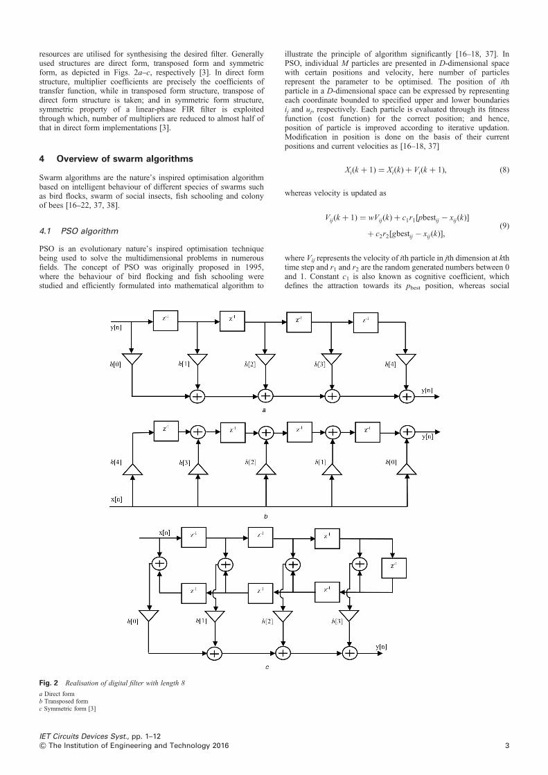
resources are utilised for synthesising the desired filter. Generallyused structures are direct form, transposed form and symmetricform, as depicted in Figs. 2a–c, respectively [3]. In direct formstructure, multiplier coefficients are precisely the coefficients oftransfer function, while in transposed form structure, transpose ofdirect form structure is taken; and in symmetric form structure,symmetric property of a linear-phase FIR filter is exploitedthrough which, number of multipliers are reduced to almost half ofthat in direct form implementations [3].
4 Overview of swarm algorithms
Swarm algorithms are the nature’s inspired optimisation algorithmbased on intelligent behaviour of different species of swarms suchas bird flocks, swarm of social insects, fish schooling and colonyof bees [16–22, 37, 38].
4.1 PSO algorithm
PSO is an evolutionary nature’s inspired optimisation techniquebeing used to solve the multidimensional problems in numerousfields. The concept of PSO was originally proposed in 1995,where the behaviour of bird flocking and fish schooling werestudied and efficiently formulated into mathematical algorithm to
Fig. 2 Realisation of digital filter with length 8
a Direct formb Transposed formc Symmetric form [3]
IET Circuits Devices Syst., pp. 1–12& The Institution of Engineering and Technology 2016
illustrate the principle of algorithm significantly [16–18, 37]. InPSO, individual M particles are presented in D-dimensional spacewith certain positions and velocity, here number of particlesrepresent the parameter to be optimised. The position of ithparticle in a D-dimensional space can be expressed by representingeach coordinate bounded to specified upper and lower boundariesij and uj, respectively. Each particle is evaluated through its fitnessfunction (cost function) for the correct position; and hence,position of particle is improved according to iterative updation.Modification in position is done on the basis of their currentpositions and current velocities as [16–18, 37]
Xi(k + 1) = Xi(k)+ Vi(k + 1), (8)
whereas velocity is updated as
Vij(k + 1) = wVij(k)+ c1r1[pbestij − xij(k)]
+ c2r2[gbestij − xij(k)],(9)
where Vij represents the velocity of ith particle in jth dimension at kthtime step and r1 and r2 are the random generated numbers between 0and 1. Constant c1 is also known as cognitive coefficient, whichdefines the attraction towards its pbest position, whereas social
3

Fig. 3 Flow chart of proposed methodology using hybrid method
Table 2 Device utilisation summary
Logic utilisation Used Available Utilisation,%
number of slice flip-flops 420 9312 4number of four-input LUTs 1875 9312 20number of occupied slices 1194 4656 25number of slices containing onlyrelated logic
1194 1194 100
number of slices containingunrelated logic
0 1194 0
total number of four-input LUTs 1905 9312 20number used as logic 1875number used as a route-thru 30number of bonded input outputblocks (IOBs)
31 232 13
number of global clock MUX buffer(BUFGMUXS)
1 24 4
average fan-out of non-clock nets 1.85
coefficient c2 determines the influence towards swarm, and w is theinertia weight [16–18, 37].
4.2 ABC algorithm
The concept of ABC algorithm was firstly introduced by Karaboga,based on the foraging behaviour of honey bees for solving
Table 1 Design statistics and cell usage
input output (IOs) 31basic elements (BELS) 5433ground (GND) 1inversion (INV) 282LUT1 29LUT2 1375LUT3 94LUT4 96MULT_AND 122-to-1 multiplexer for carry logic with general output (MUXCY) 1731plus collector supply line voltage in a common NPN circuit (VCC) 1XOR for carry logic with general output (XORCY) 1812flip flops/latches 420D flip-flop with clock enable and asynchronous clear (FDCE) 420clock buffers 1global clock buffer (BUFGP) 1in out (IO) buffers 30input buffer (IBUF) 16output buffer (OBUF) 14
4
multimodal and multidimensional problem [38]. In ABC, the foodsource N is defined in D-dimension, where number of dimensionrepresents the parameters to be optimised. Then, food sourcepositions are randomly initialised. The total generated solutions areexpressed using N ×D matrix. Consider Si = (Si1, Si2, …, SiD),which exhibits the ith solution of population in D-dimension,where i = 1, …, N [20–22, 37]. Initially, populations are generatedusing [37]
Si,j = Smin ,j + rand(0, 1)× (Smax ,j − Smin ,j), (10)
where Smin,j and Smax,j show the lower and upper limit of jthdimension, respectively. Food source is assigned to employed beesto calculate the fitness function (nectar amount). Now, new foodsource (Vi,) is determined, using employed bee (Si) from itscurrent position to the neighbourhood position as [20–22, 37]
Vi,j = Si,j + fi,j × (Si,j − Sk,j), (11)
where fi, j is randomly selected number with range (1, −1), whilerange of k is (1, 2, …, N) and D is (1, 2, …, M ). Then, positionwith best fitness value is selected by comparison and assigned as anew population member. If the new position (solution) providesminimum value of objective function than previously obtained,then old position is replaced by new one. Similarly, onlooker beesalso select the quality of food through comparison by means ofprobability in fitness function. This can be expressed as [20–22, 37]
pi =0.9× Fitnessi
Fitnessmax × 0.1. (12)
After selecting the food source Si by onlooker, modification in Si isdone by (13), and the onlooker bee also employs greedy selection. Ifoptimum value of fitness function is not obtained in specified no ofsteps, called as ‘limit’, then the food source are abandoned and thebee becomes scout bee. Then, scout bee provides new solution offood source randomly [20–22, 37]. Procedure is repeated until thebest solution representing improved value of objective function isobtained.
5 Hybrid optimisation method for two-channelfilter bank
This hybrid method is based on joint approach of ABC and PSO.Originally, this concept of hybrid methodology was given by Rafiet al. and used in the design of multirate filter bank [11, 16].Superiority of this algorithm lies on its search mechanism, whichensures the optimality of solution and saves from trapping in localminima. In this method, concept of limit (control parameter forgeneration of scouts) and trials (iterations) of scout bee from ABC
IET Circuits Devices Syst., pp. 1–12& The Institution of Engineering and Technology 2016

Fig. 4 Convergence of proposed hybrid method
a Variation of objective function with respect to swarm sizeb Variation of RE with respect to swarm sizec Variation of objective function with respect to iterationsd Variation of RE with respect to iterations
are employed on the updated particles of PSO [11, 16]. Whenposition of particles updated as according to PSO algorithmdescribed in Section 4.1, for a given number of trials and withinthe limit defined in ABC algorithm given in Section 4.2, fails tohave optimum value of fitness function in limit numbers of trial,then the position and velocity are replaced by particles having bestsolution (gbest) [11, 16]. In this way, population matrixes areupdated according to velocity updation, after that values invelocity and position matrix are checked for limits. Finally,objective function is evaluated by using new population, and thequality of respective solutions is checked. During this procedure, ifsolution is not improved, then its current value is replaced by gbestvalue, and the velocity corresponding to that unimproved solutionis replaced by the current velocity corresponding to gbest. In thisway, the swarm is updated which exhibits the property of optimalpoint exploration that finally controls the solutions from trappingin local minima. However, the results obtained from theseswarm-based techniques are not proved as global; therefore,average of 10 solutions has been taken as optimised results. In thispaper, two-channel filter bank has been designed using this hybridPSO method, which utilises the efficiency of PSO and ABC bydesigning optimal prototype filter, and then filter bank.
5.1 Problem formulation
In this hybrid method, particles are initialised with random velocityand position within the limit of passband edge frequency (ωp) and
IET Circuits Devices Syst., pp. 1–12& The Institution of Engineering and Technology 2016
stopband edge frequency (ωs) as lower and upper limit calculatedas [3, 6–8, 11–14]
vs =(1+ RF)p
2(13)
and
vp =p
2. (14)
Then, order of a prototype filter is estimated using As, ωp and ωs
[3, 6–8, 11–14]
N = (As − 7.95)
14.95Df, (15)
where
Df =vs − vp
( )
2. (16)
Here, particles represent the cut-off frequency (ωc), which is used todesign efficient prototype filter using window function, and thederived continuous filter coefficients are quantised and representedin CSD and FCSD form. These CSD and FCSD quantised filtercoefficients are optimised such that the magnitude response ofprototype filter approach to 0.707. For this purpose, an objective
5

Fig. 5 Comparison of magnitude response and reconstruction error of proposed prototype filter designed with continuous coefficients with different WL
a Magnitude response of proposed prototype filter for order N = 30 with different WLsb Zoom plot of RE with different WLs
Table 4 Performance parameters in analysis of the of differentstructures for proposed prototype filter with WL 14
Parameters Directform
Transposedform
Symmetricform
Availableresources
slices 683 414 527 4656flip-flops 420 778 420 9312LUTs 865 765 569 9312adder 30 30 30 –multiplier 31 31 15 –
function is constructed as error between the magnitude responseimaging (MRI) of a prototype filter H (ejπ/2) in ideal conditiongiven by (20) and magnitude response (MRD) of designed filter atquadrature frequency.
H0(ejp/2)
∣∣ ∣∣ = 0.707. (17)
Thus, the objective function is defined as
w = abs MRI−MRD[ ]. (18)
Table 3 Parameter variations of proposed filter with different WLs
Filters N As(dB) AD RE
WL = 8 30 54.81 0.097054 0.03006WL = 10 30 61.65 0.008 0.0203WL = 12 30 70.38 0.0045 0.0053WL = 14 30 75.71 0.0027 0.0025WL = 16 30 78.12 0.0017 0.0023continuous coefficients [13] 30 81.98 0.00163 0.0019
Table 5 Performance parameters of proposed prototype filter in CSDand FCSD space in symmetric structure with order 30
Parameters CSD(14 bit)
CSD(12 bit)
FCSD(14 bit)
CSD(12 bit)
Availableresources
slices 816 629 786 599 4656flip-flops 420 348 420 348 9312LUTs 1167 849 1134 816 9312adder 62 51 60 49 –multiplier 0 0 0 0 –
IET Circuits Devices Syst., pp. 1–126 & The Institution of Engineering and Technology 2016
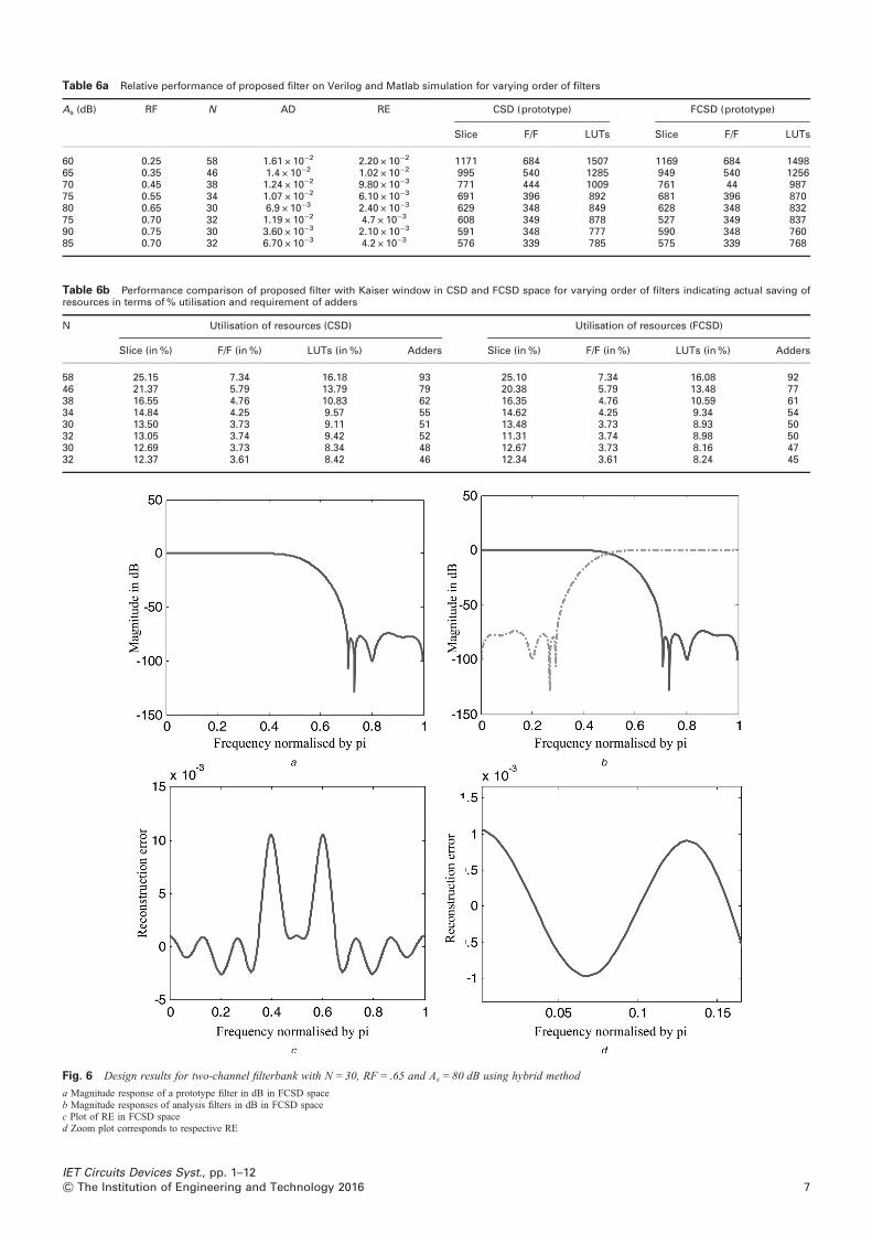
Table 6a Relative performance of proposed filter on Verilog and Matlab simulation for varying order of filters
As (dB) RF N AD RE CSD (prototype) FCSD (prototype)
Slice F/F LUTs Slice F/F LUTs
60 0.25 58 1.61 × 10⁻² 2.20 × 10⁻² 1171 684 1507 1169 684 149865 0.35 46 1.4 × 10⁻² 1.02 × 10⁻² 995 540 1285 949 540 125670 0.45 38 1.24 × 10⁻² 9.80 × 10⁻³ 771 444 1009 761 44 98775 0.55 34 1.07 × 10⁻² 6.10 × 10⁻³ 691 396 892 681 396 87080 0.65 30 6.9 × 10⁻³ 2.40 × 10⁻³ 629 348 849 628 348 83275 0.70 32 1.19 × 10⁻² 4.7 × 10⁻³ 608 349 878 527 349 83790 0.75 30 3.60 × 10⁻³ 2.10 × 10⁻³ 591 348 777 590 348 76085 0.70 32 6.70 × 10⁻³ 4.2 × 10⁻³ 576 339 785 575 339 768
Fig. 6 Design results for two-channel filterbank with N = 30, RF = .65 and As = 80 dB using hybrid method
a Magnitude response of a prototype filter in dB in FCSD spaceb Magnitude responses of analysis filters in dB in FCSD spacec Plot of RE in FCSD spaced Zoom plot corresponds to respective RE
Table 6b Performance comparison of proposed filter with Kaiser window in CSD and FCSD space for varying order of filters indicating actual saving ofresources in terms of% utilisation and requirement of adders
N Utilisation of resources (CSD) Utilisation of resources (FCSD)
Slice (in %) F/F (in%) LUTs (in %) Adders Slice (in %) F/F (in %) LUTs (in%) Adders
58 25.15 7.34 16.18 93 25.10 7.34 16.08 9246 21.37 5.79 13.79 79 20.38 5.79 13.48 7738 16.55 4.76 10.83 62 16.35 4.76 10.59 6134 14.84 4.25 9.57 55 14.62 4.25 9.34 5430 13.50 3.73 9.11 51 13.48 3.73 8.93 5032 13.05 3.74 9.42 52 11.31 3.74 8.98 5030 12.69 3.73 8.34 48 12.67 3.73 8.16 4732 12.37 3.61 8.42 46 12.34 3.61 8.24 45
IET Circuits Devices Syst., pp. 1–127& The Institution of Engineering and Technology 2016

Fig. 7 Design results for two-channel filterbank with N = 32, RF = 0.70 and As = 85 dB using hybrid method
a Magnitude response of a prototype filter in dB in FCSD spaceb Magnitude responses of analysis filters in dB in FCSD spacec Plot of RE in FCSD spaced Zoom plot corresponds to respective RE
Here, initially a prototype filter is designed using Kaiser windowfor a given specifications of stopband attenuation and channeloverlapping; then the derived filter coefficients are quantised, and
Table 7 Relative performance of proposed filter with different window function
Algorithm Window As (dB) Order
hybrid method Kaiser 80 30hybrid method Kaiser 85 32hybrid method Blackman 80 30hybrid method Blackman 85 32hybrid method Cosh 80 30hybrid method Cosh 85 32hybrid method Exponential 80 30hybrid method Exponential 85 32ABC Kaiser 80 30ABC Kaiser 85 32ABC Blackman 80 30ABC Blackman 85 32ABC Cosh 80 30ABC Cosh 85 32ABC Exponential 80 30ABC Exponential 85 32PSO Kaiser 80 30PSO Kaiser 85 32PSO Blackman 80 30PSO Blackman 85 32PSO Cosh 80 30PSO Cosh 85 32PSO Exponential 80 30PSO Exponential 85 32
8
their magnitude response (MRD) at quadrature frequency iscomputed and compared with MRI. If this is comparable, thenremaining filters are designed using this quantised prototype filter.
s for different window functions
RF AD RE CPU (s)
0.65 6.9 × 10⁻³ 2.40 × 10⁻³ 20.39410.70 6.70 × 10⁻³ 4.2 × 10⁻³ 20.1180.65 3.601 × 10⁻³ 1.811 × 10⁻³ 20.4210.70 4.870 × 10⁻³ 2.621 × 10⁻³ 20.1420.65 6.145 × 10⁻² 5.112 × 10⁻³ 20.1460.70 7.543 × 10⁻³ 2.922 × 10⁻³ 21.0040.65 8.291 × 10⁻² 5.41 × 10⁻³ 20.4820.70 7.891 × 10⁻³ 4.721 × 10⁻³ 20.1540.65 3.22 × 10⁻² 7.271 × 10⁻³ 23.0560.70 7.69 × 10⁻³³ 6.40 × 10⁻³ 22.9760.65 8.77 × 10⁻³ 7.91 × 10⁻³ 23.1240.70 6.70 × 10⁻³ 5.17 × 10⁻³ 23.4460.65 6.39 × 10⁻³ 5.721 × 10⁻³ 23.0580.70 7.413 × 10⁻³ 5.922 × 10⁻³ 23.1160.65 7.91 × 10⁻³ 8. 21 × 10−3 22.8480.70 8.55 × 10⁻³ 7.22 × 10⁻³ 22.8620.65 8.874 × 10⁻³ 2.573 × 10⁻³ 21.8180.70 7.667 × 10⁻² 2.6983 × 10⁻³ 21.960.65 8.296 × 10⁻³ 2.871 × 10⁻³ 21.8410.70 9.047 × 10⁻³ 2.9123 × 10⁻³ 21.9310.65 2.227 × 10⁻² 6.721 × 10⁻³ 21.8680.70 2.624 × 10⁻² 4.658 × 10⁻³ 21.9150.65 1.678 × 10⁻² 6.394 × 10⁻³ 21.6380.70 1.873 × 10⁻² 4.110 × 10⁻³ 21.784
IET Circuits Devices Syst., pp. 1–12& The Institution of Engineering and Technology 2016

The proposed method designs multiplierless QMF that gives less REin single optimisation. This procedure can be summarised into thefollowing steps and flowchart as described in Fig. 3.
Step 1: Specify the design specifications such as stopbandattenuation (As) RF, N, ωs and ωp using (16)–(18). Population sizexi, iteration, limit and trials for scout bee.Step 2: Set the parameters for optimisation algorithm, initialisepopulation as xi and iteration. Here, population represents cut-offfrequency taking randomly in the range of ωp and ωs as lower andupper limit, respectively.Step 3: Employ window functions to calculate the coefficients ofprototype filter. Convert it into the quantised filter coefficients andrepresent as CSD and FCSD.Step 4: Evaluate the fitness function j for each value of xi from (21).Step 5: Update velocity and particle using (10) and (11), respectively.Step 6: Compare the fitness value of present fitness j (xi(t + 1)) withPbest fitness j (xi(t)). If current value is better than the previous one,i.e. j (xi(t + 1)) < j (xi(t)), assign Pbest as present position andupdate gbest. If previous value was better than current one, i.e. j(xi(t + 1)) >j (xi(t)), then increase trail counter by 1.Step 7: Check whether counter is reached at maximum limit or not. Ifnot, go to Step 9. If yes, replace velocity and position of particle,assign Pbest as present position and update gbest.Step 8: Check whether the tolerance is ≤j. If yes, design QMF bankand find optimised value of quantised coefficients and represent it intoCSD and FCSD. If no, go back to Step 6 and follow the next steps.
Designed filter is also synthesised in FPGA. Spartan 3E starterboard with XC3S500E-4-FG320 is taken for realisation of a
Fig. 8 Parameter variations of proposed prototype filter using hybrid method in
a Variations in terms of number of occupied slicesb Variations in terms of number of occupied LUTsc Variations in terms of number of occupied Flip-Flopsd Variations in terms of number of Adders
IET Circuits Devices Syst., pp. 1–12& The Institution of Engineering and Technology 2016
prototype filter using Verilog. Firstly, different structures forproposed prototype filter are synthesised, i.e. direct form, transposedform and symmetric form, respectively [3]. Performance of thesestructures is compared in terms of slices, adder/substractor, numberof flip-flop and LUTs. The detail description with device summeryand performance is shown in Tables 1 and 2. Slices give theinformation regarding area of utilisation, and also indicate the usednumber of slices out of given number of slices for the target FPGAused. Utilisation of Flip-flop shows the number of registers required,and LUTs is the look up tables. On the basis of observations andanalytical facts in this paper, symmetric structure is chosen asefficient structure for realisation. While the application of CSD andFCSD makes filter multiplier less.
6 Results and discussions
Several design examples are included to demonstrate the efficiencyof proposed algorithm in CSD and FCSD space. Performanceparameters such as amplitude distortion, and reconstruction error(RE) computed using respective (22) and (23), are measured tocompare and analyse the effectiveness of proposed method, whilecomputation time is measured as central processing unit (CPU)time in seconds.
RE = maxv
10log10 H0(ejv)
∣∣ ∣∣2 + H0(ej(v−p))
∣∣ ∣∣2( ){ }. (19)
eam(v) = 1− H0 ejv( )∣∣ ∣∣2 + H0 ej(v−p)( )∣∣ ∣∣2( )
. (20)
FPGA with CSD and FCSD for varying orders with WL = 12
9

Table 8 Low pass (LP) filter coefficient for N = 30
h(n) Continuous coefficients CSDequivalent
Binaryequivalent
h(1) = h(30) −2.40489883441211e-05 −00000000000 100000000000h(2) = h(29) −0.000125579104961639 −00000000000 100000000000h(3) = h(28) 0.000477614559451155 00000000000+ 000000000001h(4) = h(27) 0.000622780499123109 00000000000+ 000000000001h(5) = h(26) −0.00252145586450629 000000000−0− 111111111011h(6) = h(25) −0.00128701262054909 000000000−0+ 111111111101h(7) = h(24) 0.00836836098311965 0000000+000+ 000000010001h(8) = h(23) 0.000572533130657355 00000000000+ 000000000001h(9) = h(22) −0.0212176414068199 00000−0+0+0+ 111111010101h(10) = h(21) 0.00571505185658366 0000000+0−00 000000001100h(11) = h(20) 0.0459520285038893 0000+0−000−0 000001011110h(12) = h(19) 0.0280089646265064 00000−00+00− 111111000111h(13) = h(18) 0.0987589219271596 000−0+00−0−0 111100110110h(14) = h(17) 0.118178823282509 000+000−00+0 000011110010h(15) = h(16) 0.472056431723514 0+000−00+00− 001111000111
Table 9b Power consumption in the proposed method
Frequency 5 MHz 8 MHz 10 MHz 14 MHz
power, mW 41 58 61 79
For designing the filter, parameters of the proposed hybrid PSOalgorithm are chosen based on experiment, where convergence ofobjective function and RE is observed as shown in Fig. 4. InFigs. 4a and b, convergence of hybrid algorithm with respect toswarm size is shown. Here, swarm size is varied in step size of 5,up to 50 population size, while the number of iterations is kept asconstant. Similarly, Figs. 4c and d show the convergence ofalgorithm for varying iteration with step size of 10, whilepopulation was kept constant. Finally, based on these observations,in this paper, population size is kept at 50; maximum number ofiterations has been chosen as 100.
6.1 Design examples
Example I: The prototype filter of a QMF has been designed withAs = 80 dB and RF = 0.65. The stopband edge frequency (ωs) iscomputed by (18), which is equal to 0.775π and (ωp) is 0.5π.Using these values, N is estimated as 30.
Performance of the proposed filter using hybrid method is alsoexamined for different WL such as 8, 10, 12, 14 and 16 as shownin Fig. 5a, while impact of different WL on the performance of
Table 9a Devise utilisation summary and performance summery ofproposed filter
Logic device utilisation summary Delay, power and frequencyrequired to implement the
circuit
logic utilisation used available minimum period 69.872ns
number of slice flipflops
420 9312 maximumfrequency
14.312MHz
number of four-inputLUTs
1875 9312 minimum inputarrival time before
clock
3.158 ns
number of occupiedslices
1194 4656 maximum outputrequired time after
clock
4.283 ns
number of slicescontaining onlyrelated logic
1194 1194 maximum delay 0.20100
number of slicescontaining unrelatedlogic
0 1194 total power 80.98mW
total number offour-input LUTs
1905 9312
number used aslogic
1875
number used as aroute-thru
30
number of bondedIOBs
31 232
number ofBUFGMUXs
1 24
average fanout ofnon-clock nets
1.85
10
designed filter on RE is depicted in Fig. 5b. It can be observedfrom Fig. 5 that WL= 8 gives worst performance, while WL 12and 14 give comparable performance, while WL 16 providesalmost same performance. So in this paper, WL of 14 and 12 issuggested as good choice for implementing filter using proposedmethodology. The obtained results are also summarised in Table 3.
The proposed optimal filter using hybrid method algorithm is alsosynthesised using Verilog in Spartan 3E XC3S500E target FPGAdevice. Three different structures: direct form, transposed form andsymmetric form are synthesised for designing a filter as illustratedin design Example I. The obtained results are summarised in Table 4.
From Table 4, it is observed that the symmetric structure is anefficient structure for realising the proposed digital filter as itconsumes less amount of slices and multipliers, when comparedwith direct and transposed form. Representation of proposed filtercoefficients in CSD and FCSD eliminates the multiplier from thecircuit, and circuit becomes multiplier less. This multiplierlesscircuit is synthesised using symmetric structure, and the results aresummarised in Tables 5 and 6.
Example II: A QMF has been designed with As = 80 dB and RF =0.65. ωs is computed as 0.775π and ωp is 0.5π. Using these values,N is estimated as 30. The designed results obtained with theproposed scheme are shown in Fig. 6.
Example III: In this design example, QMF has been designed withAs = 85 dB and RF = 0.60. In this case, order of filter is 32. Thesequantised coefficients are represented in CSD and FCSD forms.The simulation results obtained are shown in Fig. 7.
Similarly, Kaiser window has been used for designing QMF inFCSD space for different design specifications. The design resultsobtained are tabulated in Table 6a, while the design resultsobtained using other windows such as Blackman, Cosh andExponential are listed in Table 7.
The designed filter is implemented on Xilinx using Verilog, andthe obtained results are summarised in Table 6, in terms of slices,flip-flops and LUTs for the case of CSD and FCSD. In Table 4a,for different values of RF, orders of filter are calculated and finallytwo-channel filter bank is designed. It is evident from Table 6athat the proposed filter based on hybrid algorithm utilises lessslices and LUTs, ∼344 slices and 770 LUTs, respectively. Thebest amplitude distortion obtained with this technique is 1.69 ×10⁻³ for N = 144 and M = 8 with As = 80.
In Table 6b, performance of the proposed filter is compared inCSD and FCSD space in terms of hardware resources such asslices, LUTs registers, flip-flops and total numbers of adders/substractor, and is also shown in Fig. 8. It is observed that the
Table 10a Relative performance of proposed filter with differentexisting algorithms
Filter N WL Total adder Adder gain (%)
algorithm in [38] 33 13 79algorithm in [39] 27 13 67 15.18algorithm in [40] 29 12 57 27.84algorithm in [41] 28 8 56 29.11algorithm in [42] 28 11 54 31.64algorithm in [43] 29 10 29 62.13algorithm in [44] 59 10 69 –proposed (CSD) (As = 80) 30 12 51 35.44proposed (FCSD) (As = 80) 30 12 50 36.70proposed (CSD (As = 85) 32 12 46 41.772proposed (FCSD) (As = 85) 32 12 45 43.07
IET Circuits Devices Syst., pp. 1–12& The Institution of Engineering and Technology 2016

Table 10b Performance comparison of proposed multiplierless filter with considering more description of the hardware resources
Filter WL PRE Adder Slice LUT Delay (ns) Flip-flops
algorithm in [45] 14 – 416 – 7136 – –algorithm in [46] 12 5.122 × 10⁻³ 44 – – – –algorithm in [47] 8 – – 287 379 2.713 196algorithm in [48] 14 9.118 × 10⁻³ 486 – 9584 – –algorithm in [49] 12 7.126 × 10⁻² 223 – 2048 – –algorithm in [50] 14 – 561 – 4488 – –proposed 12 2.10 × 10⁻³ 96 1171 1507 70 684
number of slices, LUTs and adders are less in FCSD when comparedwith CSD. However, the total number of required registers(flip-flops) remains the same.
The proposed method is also applicable for higher order filters,which has been tested for a prototype filter with higher order suchas N = 100. For this case, AD = 6.03 × 10⁻³, RE = 8.145 × 10⁻³
and 120 numbers of adder are required for the implementation. Ithas been observed that, for higher orders filter also, number ofadders and response of filter directly depends on size of WL.
6.2 Comparison with other methodologies
Comparison of the proposed methodology with other swarm-basedtechniques such as PSO and ABC is shown in Table 7. Whereprototype filter of a QMF has been designed with different valueof N, As and RF. It has been observed that the hybrid methodoutperforms among PSO and ABC algorithms with significantimprovement in RE and amplitude distortions. In Table 8, oneexample of designed filter has been tabularised for analysing thedistributed SPTs for respective filter coefficients, the tabulated –and + signs show the number of SPTs here. Tables 9a and bconsist of devise utilisation and performance summary of designedfilter on FPGA. For this purpose, the generated file has beensynthesised on Xilinx Spartan 3E target device. Performance ofthe proposed prototype is also compared with other methods [39–44]. Results are compared and summarised in Table 10a.Reduction in number of adders is indicated by adder gain,computed as
Addergain =Totaladder − Calculatedadder
Totaladder× 100. (21)
From Table 10, it can be observed that the multiplierless prototypefilter in a two-channel filter bank designed by the hybrid techniquewith 12 bit of WL requires fewer amounts of adders: 46 withadder gain of 41.77%, while by FCSD, required number of addersare 45, with adder gain of 43%. In literature, for the design of amultiplier less two-channel filter bank, many techniques have beenreported, where two separate optimisation methods have been usedwith complex objective function, which consumes large run time.While in the proposed method, single optimisation is employedthat results in less computation time with significant improvementin amplitude distortion and RE. In Table 10b, performance of theproposed multiplier less filters considering more description ofhardware resources for comparing the performance with otherFPGA-based work is shown.
7 Conclusion
In this paper, an optimal design of a prototype filter for atwo-channel filter bank is presented using hybrid PSO algorithm.The coefficients are quantised and optimised using singleoptimisation algorithm. Proposed prototype filter has also beensynthesised in FPGA using target XC3S500E-4-FG320 device.Symmetric structure with WL 12 has been reported as good choicein realisation of the prototype filter. Several design examples withvarious window function using swarm-based techniques have also
IET Circuits Devices Syst., pp. 1–12& The Institution of Engineering and Technology 2016
been examined for designing the prototype filter in CSD and FCSDspace to further record the significance of proposed methodology.The performance of proposed hybrid method-based prototype filteris also compared with the existing algorithms, and it has beenfound that the designed prototype filter using hybrid methodconsumes less number of hardware resources and satisfies thedesired frequency response characteristics.
8 References
1 Kong, D., Xia, X.-G., Jiang, T., et al.: ‘Channel estimation in CP-OQAM-OFDMsystems’, IEEE Trans. Signal Process., 2014, 62, (21), pp. 5775–5786
2 Blanco-Velasco, M., Cruz-Roldán, F., Moreno-Martínez, E., et al.: ‘Embeddedfilter bank-based algorithm for ECG compression’, Signal Process., 2008, 88,(6), pp. 1402–1412
3 Mitra, S.K., Kuo, Y.: ‘Digital signal processing: a computer-Based approach’(McGraw-Hill, New York, 2006, 2nd edn.)
4 Creusere, C.D., Mitra, S.K.: ‘A simple method for designing high-quality prototypefilters for M-band pseudo QMF banks’, IEEE Trans. Signal Process., 1995, 43, (4),pp. 1005–1007
5 Jain, A., Saxena, R., Saxena, S.C.: ‘A simple alias-free QMF system withnear-perfect reconstruction’, J. INDIAN Inst. Sci., 2005, 85, (1), pp. 1–10
6 Kumar, A., Singh, G.K., Anand, R.S.: ‘Near perfect reconstruction quadraturemirror filter’, Int. J. Electr. Comput. Energ. Electron. Commun. Eng., 2008, 2,(1), pp. 25–28
7 Kumar, A., Singh, G.K., Kuldeep, B.: ‘An improved and simplified approach fordesigning cosine modulated filter bank using window technique’, J. Math.Model. Algorithms, 2011, 10, (3), pp. 213–226
8 Kumar, A., Kuldeep, B.: ‘Design of M-channel cosine modulated filter bank usingmodified exponential window’, J. Franklin Inst., 2012, 349, (3), pp. 1304–1315
9 Shaeen, K., Elias, E.: ‘Prototype filter design approaches for near perfectreconstruction cosine modulated filter banks – a review’, J. Signal Process.Syst., 2014, 81, (2), pp. 183–195
10 Sahu, O.P., Soni, M.K., Talwar, I.M.: ‘Marquardt optimization method to designtwo-channel quadrature mirror filter banks’, Digit. Signal Process., 2006, 16, (6),pp. 870–879
11 Kumar, A., Rafi, S.M., Singh, G.K.: ‘A hybrid method for designing linear-phasequadrature mirror filter bank’, Digit. Signal Process., 2012, 22, (3), pp. 453–462
12 Kumar, A., Singh, G.K., Anand, R.S.: ‘An improved method for the design ofquadrature mirror filter banks using the Levenberg-Marquardt optimization’,Signal, Image Video Process., 2013, 7, (2), pp. 209–220
13 Bergen, S.W.A., Antoniou, A.: ‘An efficient closed-form design method forcosine-modulated filter banks using window functions’, Signal Process., 2007,87, (5), pp. 811–823
14 Kumar, A., Singh, G.K., Anand, R.S.: ‘A closed form design method for thetwo-channel quadrature mirror filter banks’, Signal, Image Video Process., 2009,5, (1), pp. 121–131
15 Manoj, V.J., Elias, E.: ‘Design of multiplier-less nonuniform filter banktransmultiplexer using genetic algorithm’, Signal Process., 2009, 89, (11),pp. 2274–2285
16 Upendar, J., Gupta, C.P., Singh, G.K.: ‘Design of two-channel quadrature mirrorfilter bank using particle swarm optimization’, Digit. Signal Process., 2010, 20,(2), pp. 304–313
17 Rafi, S.M., Kumar, A., Singh, G.K.: ‘An improved particle swarm optimizationmethod for multirate filter bank design’, J. Franklin Inst., 2013, 350, (4),pp. 757–769
18 Tan, F., Zhang, T., Gao, C., et al.: ‘Optimal design of cosine modulated filter banksusing quantum-behaved particle swarm optimization algorithm’. 2011 FourthInternational Congress on Image and Signal Processing IEEE, 2011,pp. 2280–2284
19 Zhang, T., Tan, F., Yi, C., et al.: ‘An optimized design of non-uniform filter banksbased on memetic algorithm’. 2013 Sixth International Congress on Image andSignal Processing (CISP) IEEE, 2013, pp. 1194–1199
20 Agrawal, S.K., Sahu, O.P.: ‘Artificial bee colony algorithm to design two-channelquadrature mirror filter banks’, Swarm Evol. Comput., 2015, 21, pp. 24–31
21 Kuldeep, B., Singh, V.K., Kumar, A., et al.: ‘Design of two-channel filter bankusing nature inspired optimization based fractional derivative constraints’, ISATrans., 2015, 54, pp. 101–116
22 Kuldeep, B., Kumar, A., Singh, G.K.: ‘Design of multi-channel cosine-modulatedfilter bank based on fractional derivative constraints using cuckoo searchalgorithm’, Circuits Syst. Signal Process., 2015, 34, (10), pp. 3325–3351
11

23 Avizienis, A.: ‘Signed-digit number representations for fast parallel arithmetic’,IEEE Trans. Electron. Comput., 1961, EC-10, (3), pp. 389–400
24 Hewlitt, R.M., Swartzlantler, E.S.: ‘Canonical signed digit representation for FIRdigital filters’. 2000 IEEE Workshop on SiGNAL PROCESSING SYSTEMS.SiPS 2000. Design and Implementation (Cat. No.00TH8528) IEEE, 2000,pp. 416–426
25 Park, S.Y., Cho, N.I.: ‘Design of signed powers-of-two coefficient perfectreconstruction QMF bank using CORDIC algorithms’, IEEE Trans. CircuitsSyst. I Regul. Pap., 2006, 53, (6), pp. 1254–1265
26 Pan, S.-T.: ‘A canonic-signed-digit coded genetic algorithm for designing finiteimpulse response digital filter’, Digit. Signal Process., 2010, 20, (2), pp. 314–327
27 Goel, N., Nandi, A.: ‘Design of FIR filter using FCSD representation’. 2015 IEEEInt. Conf. on Computational Intelligence & Communication Technology IEEE,2015, pp. 617–620
28 Ababneh, J.I., Bataineh, M.H.: ‘Linear phase FIR filter design using PSO andgenetic algorithms’, Digit. Signal Process., 2008, 18, (4), pp. 657–668
29 Mercier, P., Kilambi, S.M., Nowrouzian, B.: ‘Optimization of FRM FIR digitalfilters over CSD and CDBNS multiplier coefficient spaces employing a novelgenetic algorithm’, J. Comput., 2007, 2, (7), pp. 20–31
30 George, J.T., Elias, E.: ‘Reconfigurable channel filtering and digital downconversion in optimal CSD space for software defined radio’, AEU—Int. J. Electron. Commun., 2014, 68, (4), pp. 312–321
31 Soleimani, A.: ‘Combine PSO and CSD to design finite impulse response filter’,Soft Comput., 2014, 19, (2), pp. 407–419
32 Bindiya, T.S., Elias, E.: ‘Modified metaheuristic algorithms for the optimal designof multiplier-less non-uniform channel filters’, Circuits Syst. Signal Process., 2013,33, (3), pp. 815–837
33 Bindiya, T.S., Elias, E.: ‘Design of multiplier-less sharp transition widthnon-uniform filter banks using gravitational search algorithm’, Int. J. Electron.,2014, 102, (1), pp. 48–70
34 George, J.T., Elias, E.: ‘Design of multiplier-less continuously variable bandwidthsharp FIR filters using modified harmony search algorithm’, Int. J. Inf. Technol.Manag., 2014, 14, (1), pp. 5–25
35 Misra, D., Dhabal, S., Venkateswaran, P.: ‘Quadrature mirror filter bank withcanonical signed digit representation using linear optimization algorithm’. Proc.of the 2015 Third Int. Conf. on Computer, Communication, Control andInformation Technology (C3IT) IEEE, 2015, pp. 1–6
36 Reddy, K.S., Sahoo, S.K.: ‘An approach for FIR filter coefficient optimizationusing differential evolution algorithm’, AEU—Int. J. Electron. Commun., 2015,69, (1), pp. 101–108
37 Karaboga, D.: ‘An idea based on honey bee swarm for numerical optimization’,Tech. Rep., TR06, Erciyes Univ., 2005, (TR06), p. 10
12
38 Feng, Z.G., Teo, K.L.: ‘A discrete filled function method for the design of FIRfilters with signed-powers-of-two coefficients’, IEEE Trans. Signal Process.,2008, 56, (1), pp. 134–139
39 Xu, F., Xilinx Asia Pacific Pte. Ltd., S., Chang, C.H., Jong, C.C.: ‘Design oflow-complexity FIR filters based on signed-powers-of-two coefficients withreusable common subexpressions’, Comput. Des. Integr. Circuits Syst. IEEETrans., 2007, 26, (10), pp. 1898–1907
40 Jheng, K.-Y., Jou, S.-J., Wu, A.-Y.: ‘A design flow for multiplier less linear-phaseFIR filters: from system specification to Verilog code’. 2004 IEEE Int. Symp. onCircuits and Systems (IEEE Cat. No.04CH37512) IEEE, 2004, pp. V-293–V-296
41 Yli-Kaakinen, J., Saramaki, T.: ‘A systematic algorithm for the design of multiplierless FIR filters’. ISCAS 2001. The 2001 IEEE Int. Symp. on Circuits and Systems(Cat. No.01CH37196) IEEE, 2001, pp. 185–188
42 Chandra, A., Chattopadhyay, S.: ‘A novel approach for coefficient quantization oflow-pass finite impulse response filter using differential evolution algorithm’,Signal Image Video Process., 2012, 8, (7), pp. 1307–1321
43 Ye, W.B., Yu, Y.J.: ‘Single-stage and cascade design of high order multiplier lesslinear phase FIR filters using genetic algorithm’, IEEE Trans. on Circuits andSystems I: Regular Papers, 2013, 60, (11), pp. 2987–2997
44 Ye, W.B., Yu, Y.J.: ‘Two-step optimization approach for the design of multiplierless linear-phase FIR filters’, IEEE Trans. on Circuits and Systems I: RegularPapers, 2015, 62, (5), pp. 1279–1287
45 Kalathil, S., Elias, E.: ‘Design of multiplier-less sharp non-uniform cosinemodulated filter banks for efficient channelizers in software defined radio’, Eng.Sci. Technol. Int. J., 2016, 19, (1), pp. 147–160
46 Sharma, I., Kumar, A., Singh, G.K.: ‘An efficient method for designingmultiplier-less non-uniform filter bank based on hybrid method using CSEtechnique’, Circuits Syst. Signal Process., 2016, pp. 1–23, doi: 10.1007/s00034-016-0351-2
47 Rashidi, B.: ‘High performance and low-power finite impulse response filter basedon ring topology with modified retiming serial multiplier on FPGA’, IET SignalProcess., 2013, 7, (8), pp. 743–753
48 Sakthivel, V., Elias, E.: ‘Design of low complexity sharp MDFT filter banks withperfect reconstruction using hybrid harmony-gravitational search algorithm’, Eng.Sci. Technol. Int. J., 2015, 18, (4), pp. 648–657
49 Bindiya, T.S., Elias, E.: ‘Meta-heuristic evolutionary algorithms for the designof optimal multiplier-less recombination filter banks’, Inf. Sci., 2016, 339,pp. 31–52
50 Illa, A., Haridas, N., Elias, E.: ‘Design of multiplier-less FIR filters withsimultaneously variable bandwidth and fractional delay’, Eng. Sci. Technol. Int.J., 2016, 19, (3), pp. 1160–1165
IET Circuits Devices Syst., pp. 1–12& The Institution of Engineering and Technology 2016