design of power factor correction circuit using · pdf fileis now part of on semiconductor and...
TRANSCRIPT

To learn more about ON Semiconductor, please visit our website at www.onsemi.com
Is Now Part of
ON Semiconductor and the ON Semiconductor logo are trademarks of Semiconductor Components Industries, LLC dba ON Semiconductor or its subsidiaries in the United States and/or other countries. ON Semiconductor owns the rights to a number of patents, trademarks, copyrights, trade secrets, and other intellectual property. A listing of ON Semiconductor’s product/patent coverage may be accessed at www.onsemi.com/site/pdf/Patent-Marking.pdf. ON Semiconductor reserves the right to make changes without further notice to any products herein. ON Semiconductor makes no warranty, representation or guarantee regarding the suitability of its products for any particular purpose, nor does ON Semiconductor assume any liability arising out of the application or use of any product or circuit, and specifically disclaims any and all liability, including without limitation special, consequential or incidental damages. Buyer is responsible for its products and applications using ON Semiconductor products, including compliance with all laws, regulations and safety requirements or standards, regardless of any support or applications information provided by ON Semiconductor. “Typical” parameters which may be provided in ON Semiconductor data sheets and/or specifications can and do vary in different applications and actual performance may vary over time. All operating parameters, including “Typicals” must be validated for each customer application by customer’s technical experts. ON Semiconductor does not convey any license under its patent rights nor the rights of others. ON Semiconductor products are not designed, intended, or authorized for use as a critical component in life support systems or any FDA Class 3 medical devices or medical devices with a same or similar classification in a foreign jurisdiction or any devices intended for implantation in the human body. Should Buyer purchase or use ON Semiconductor products for any such unintended or unauthorized application, Buyer shall indemnify and hold ON Semiconductor and its officers, employees, subsidiaries, affiliates, and distributors harmless against all claims, costs, damages, and expenses, and reasonable attorney fees arising out of, directly or indirectly, any claim of personal injury or death associated with such unintended or unauthorized use, even if such claim alleges that ON Semiconductor was negligent regarding the design or manufacture of the part. ON Semiconductor is an Equal Opportunity/Affirmative Action Employer. This literature is subject to all applicable copyright laws and is not for resale in any manner.

Application Note AN4121Design of Power Factor Correction Circuit Using FAN7527B
www.fairchildsemi.com
©2002 Fairchild Semiconductor Corporation
1. IntroductionThe FAN7527B is an active power factor correction(PFC)controller for boost PFC application which operates in thecritical conduction mode. It turns on MOSFET when theinductor current reaches zero and turns off MOSFET whenthe inductor current meets the desired input current referencevoltage as shown in Fig. 1. In this way, the input currentwaveform follows that of the input voltage, therefore a good
power factor is obtained.
1-1. Internal Block DiagramIt contains following blocks. • Error amplifier (E/A)• Zero current detection (Idet)• Switch current sensing (CS)• Input voltage sensing (MULT)• Switch drive (OUT)
Rev. 1.0.1
.
Figure 2. Block diagram of the FAN7527B
Inductor Peak Current
Inductor CurrentInductor Average Current
GatingSignal
Figure 1. Inductor Current Waveform
INV1
2
Vea(-)
Error Amp
Vref
++++−−−−
OVPCurrentDetector
Isovp=30uAIdovp=40uA
++++−−−−
Vref
Vm2 Vref~Vref+2.5V
2.25V
Static OVP
++++−−−−
EA_OUT
6
GND
)( Vref2Vm1VmVmoK
−−−−⋅⋅⋅⋅====
Multiplier
++++−−−−
Vm1
Vmo
0 ~ 3.8V
8pF
40k
++++−−−−
++++−−−−
2.5V Ref
InternalBias
Timer R
7
Vcc
5
4
3
8Vcc
Idet
CS
MULT
OUTDriveOutput
0.25V
Veao(L)=2.25V
R
Q
S
UVLO
6.5V
Zero CurrentDetector
Current SenseComparator
1.8V
2V 1.5V
12V 9V11.5V 8.5V
7.2V

AN4121 APPLICATION NOTE
2
©2002 Fairchild Semiconductor Corporation
2. Device Block Description2-1. Error Amplifier and Over Voltage Protection Block The sensed and divided output voltage is fedback to the erroramplifier inverting input(INV) to regulate the output voltage. The non-inverting input is internally biased at 2.5V.The error amp output(EA_OUT) is internally connected tothe multiplier and is pinned out for the loop compensation.Generally, the control loop bandwidth of PFC converter isset below 20Hz to get a good power factor. In this application, a capacitor is connected between INV andEA_OUT. However, in case of over voltage condition, the E/A must be saturated low as soon as possible, but the narrow E/A bandwidth slows down the response. To makethe over voltage protection fast, the soft OVP and dynamic
OVP is added. The FAN7527B monitors the current flowinginto the EA_OUT pin. If the monitored current reaches about30uA, the output of multiplier is forced to be decreased, thusreducing the input current drawn from the mains(soft OVP).If the monitored current exceeds 40uA, the OVP protectionis triggered(dynamic OVP), then the external power transistor is switched off until the current falls below about10uA. In this case, it disables some internal blocks reducingthe quiescent current of the chip to 2mA. However, if theover voltage lasts so long that the output of E/A goes below2.25V, then the protection is activated(static OVP) keepingthe output stage and the external power switch turned off.The operation of the device is re-enabled as the E/A outputgoes back into its linear region.
OV
1R
2R
INV1
2
++++−−−−
Vea(-)
Error Amp
Vref
++++−−−−
OVPCurrentDetector
Isovp=30uAIdovp=40uA
++++−−−−
Vref
Vm2 Vref~Vref+2.5V
2.25V
Static OVP
OutputStage
Multiplier
2-2. MultiplierA single quadrant, two input multiplier is the critical elementthat enables this device to get power factor correction. Oneinput of multiplier(Pin 3) is connected to an external resistordivider which monitors the rectified ac line voltage. Theother input is internally driven by a DC voltage which is thedifference between error amplifier output (Pin 2) and reference voltage, Vref. The multiplier is designed to have anextremely linear transfer curve over a wide dynamic range,0V to 3.8V for Pin 3, and 2.25V to 6V for error amplifieroutput under all line and load conditions.The multiplier output controls the current sense comparatorthreshold voltage as the ac voltage traverses sinusoidallyfrom zero to peak line. This allows the inductor peak currentto follow the ac line thus forcing the average input current tobe sinusoidal. In other words, this has the effect of forcingthe MOSFET on-time to track the input line voltage, resulting in a fixed drive output on-time, thus making the pre-converter load appear to be resistive to the ac line.
The equation below describes the relationship between multiplier output and its inputs.Vmo = K × Vm1 × (Vm2 - Vref)K : Multiplier gainVm1: Voltage at Pin 3Vm2: Error amp output voltageVmo: Multiplier output voltage
Figure 3. Error Amplifier and OVP Block

APPLICATION NOTE AN4121
3
©2002 Fairchild Semiconductor Corporation
Figure 5. Current Sense Circuit
++++−−−−
Vmo
8pF
40k4
CS
Current SenseComparator
1.8V
Rsense
2-3. Current Sense ComparatorThe current sense comparator adopts the RS latch configuration to ensure that only a single pulse appears at thedrive output during a given cycle. MOSFET drain current issensed using an external sense resistor in series with theexternal MOSFET. When the sensed voltage exceeds thethreshold set by the multiplier output, the current sense comparator turns off the MOSFET and resets the PWMlatch. The latch ensures that the output remains in a low stateafter the MOSFET drain current falls back to zero.The peak inductor current under the normal operating condition is controlled by the multiplier output, Vmo. Theabnormal operating condition occurs during pre-converter
start-up at extremely high line or as output voltage sensing islost. Under these conditions, the multiplier output and current sense threshold will be internally clamped to 1.8V.Therefore, the maximum peak switch current is limited to:
Ipk(max) = 1.8V / Rsense
In the FAN7527B, an internal R/C filter has been included toattenuate any high frequency noise that may be present onthe current waveform. This circuit block eliminates the needfor an external R/C filter otherwise required for proper operation of the circuit.
INV1
2
Vea(-)
Error Amp
Vref
OVPCurrentDetector
Isovp=30uAIdovp=40uA
++++−−−−
Vref
Vm2 Vref~Vref+2.5V
++++−−−−
EA_OUT
)( Vref2Vm1VmVmoK
−−−−⋅⋅⋅⋅====
Multiplier
Vm1Vmo
0 ~ 3.8VMULT
0.25V
Veao(L)=2.25V
Current SenseComparator
1.8V
OVP
3
Figure 4. Multiplier block

AN4121 APPLICATION NOTE
4
©2002 Fairchild Semiconductor Corporation
2-4. Zero Current DetectorFAN7527B operates as a critical conduction current modecontroller. The zero current detector switches on the externalMOSFET as the voltage across the boost inductor reverses,just after the current through the boost inductor has gone tozero. The slope of the inductor current is indirectly detectedby monitoring the voltage across an auxiliary winding andconnecting it to the zero current detector Pin 5. Once the inductor current reaches ground level, the polarityof the voltage across the winding is reversed. When the Idetinput falls below 1.5V, the comparator output is triggered tothe low state. To prevent false tripping, 0.5V hysteresis is
provided. The zero current detector input is protected internally by two clamps. The upper 7.2V clamp preventsinput over voltage breakdown while the lower 0.75V clampprevents substrate injection. An internal current limit resistorprotects the lower clamp transistor in case the Idet pin isshorted to ground accidentally. A watchdog timer function isadded to the IC to eliminate the need for an external oscillator when used in stand-alone applications. The timerprovides a means to start or restart the pre-converter automatically if the drive output has been off for more than150us after the inductor current reached zero.
Figure 6. Zero Current Detector Block
++++−−−−
5
Idet
6.5V
Zero CurrentDetector
2V 1.5V
To F/F
Vin
7.2V
2-5. Output DriveThe FAN7527B contains a single totem-pole output stagedesigned specifically for a direct drive of power MOSFET.The drive output is capable of up to 500mA peak currentwith a typical rise and fall time of 130ns, 50ns respectivelywith a 1.0nF load. Additional circuitry has been added tokeep the drive output in a sinking mode whenever the UVLOis active. This characteristic eliminates the need for an external gate pull-down resistor. Internal voltage clampingensures that the output driver is always lower than 14V whensupply voltage exceeds the rated Vgs of the external MOSFET. This eliminates an external zener diode and extrapower dissipation associated with it that otherwise isrequired for the reliable circuit operation.
3. Circuit Components Design3-1. Power stage design1) Boost inductor design
The boost inductor value is determined by the minimum
switching frequency limitation. The minimum switching frequency has to be above the audio frequency. The switching period is maximum when the input voltage ishighest at maximum load condition. TS(max) is a function ofVin(peak) and VO. It can have maximum value at highest lineor at lowest line according to VO. Check TS(max) atVin(peak_min) and Vin(peak_max) , then take the higher valuefor the maximum switching period. The boost inductor valuecan be obtained by (5)
ton
LIL peak( ) t( )
Vin peak( ) ωt( )sin
--------------------------------------------------- L2I
in peak( ) ωt( )sin
Vin peak( ) ωt( )sin
---------------------------------------------------- (1)= =
L2Iin peak( )Vin peak( )-------------------------------=

APPLICATION NOTE AN4121
5
©2002 Fairchild Semiconductor Corporation
2) Auxiliary winding design
The auxiliary winding voltage is lowest at the highest line.So the number of auxiliary winding can be obtained by (7).
3) Input capacitor design
The voltage ripple of the input capacitor is maximum whenthe line is lowest and the load is heaviest. If fsw(min) >> fac ,the input current can be assumed to be constant during aswitching period.
toff LIL peak( ) t( )
VO Vin peak( ) ωt( )sin–------------------------------------------------------------ (2)=
L2Iin peak( ) ωt( )sin
VO Vin peak( ) ωt( )sin–------------------------------------------------------------=
Iin peak( )2VOIO
η Vin peak( )⋅--------------------------------- (3)=
TS ton toff+=
2LIin peak( )1
Vin peak( )----------------------------- ωt( )sin
VO Vin peak( ) ωt( )sin–----------------------------------------------------------------+
(4)=
4LVOIO max( )η
----------------------------------------- 1
V2in peak( )
-------------------------------- 1Vin peak( ) VO Vin peak( )–( )------------------------------------------------------------------------------+
=
TS max( )
4LVOIO max( )η
----------------------------------------- 1
V2in peak( )
-------------------------------- 1Vin peak( ) VO Vin peak( )–( )------------------------------------------------------------------------------+
(5)=
L η
4fsw min( )VOIO max( )1
V2in peak( )
-------------------------------- 1Vin peak( ) VO Vin peak( )–( )------------------------------------------------------------------------------+
-------------------------------------------------------------------------------------------------------------------------------------------------------------------------------------------(6)=
NauxVCC NP⋅
VO2 2
π-----------Vin HL( )–
-------------------------------------------------= 7( )
max)_( peakinI
max)_(2 peakinI⋅⋅⋅⋅
2/ont
ont
InputCurrent
InductorCurrent
The input capacitor must be larger than the value calculatedby (8). And the maximum input capacitance is limited by theinput displacement factor(IDF), defined as IDF≡cosθ .Therefore the input capacitor must be smaller than Cin(max) calculated by (12).
Cin2
∆Vin max( )---------------------------
0
ton2
----------
∫⋅≥
Iin peak_max( )2 Iin peak_max( )⋅
ton
------------------------------------------t– dt
ton Iin peak_max( )⋅
2 ∆Vin max( )⋅----------------------------------------------≥ 8( )
L I
2O max( ) V
2O⋅ ⋅
∆Vin max( ) V3in peak_max( )⋅
-----------------------------------------------------------------------≥
Va VA Vin peak( ) ωt( )cos= = 9( )
ia Ia ωt( )cos=
iA ia ic Ia ωt( )cos ωCinVin peak( ) ωt( )sin–=+= 10( )
θ tan1– ωCinVin peak( )
Ia--------------------------------------= 11( )
Cin max( )Ia
ωVin peak( )----------------------------- cos
1–IDF( )( )tan=
2VOIO
ωV2in peak_max( )
-------------------------------------------- cos1–
IDF( )( )tan= 12( )
Figure 7. Input Current and Inductor Current Waveform during a Switching Cycle

AN4121 APPLICATION NOTE
6
©2002 Fairchild Semiconductor Corporation
Figure 8. Input voltage and current displacement due to input filter capacitance
inL
inC PFCCircuit
aiAi
AV aV++++
−−−−
++++
−−−−
Input Filter
Ci
Re
Im
aiCi
Ai
θθθθ
AV
4) Output capacitor designThe output capacitor is determined by the relation betweenthe input power and the output power. As shown in Fig. 10,the minimum output capacitance is determined by (14).
Figure 9. PFC configuration
Figure 10. Diode current and output voltage waveform
5) MOSFET and diode selectionMaximum MOSFET rms current is obtained by (15) and theconduction loss of the MOSFET is calculated by (16). WhenMOSFET turns on the MOSFET current rises slowly so theturn on loss is negligible. MOSFET turn off loss and MOSFET discharge loss are obtained by (17) and (18)respectively. The switching frequency of the critical conduction mode boost PFC converter varies according tothe line condition and load condition. Therefore the switching frequency is the average value during a lineperiod. The total MOSFET loss can be calculated by (19)and then a MOSFET can be selected considering MOSFET thermal characteristic.
And the MOSFET gate drive resistor is determined by (20).
PFCL
OA
D
OC
DI OI
++++
−−−−OV
++++
−−−−inV
inI
Pin Iin rms( )Vin rms( ) 1 cos– 2ωt( )( ) IDVO= =
IDIin rms( )Vin rms( )
VO
------------------------------------------ 1 cos– 2ωt( )( )=
IO 1 cos– 2ωt( )( )= 13( )
))2cos(1()( tII OavgD ωωωω−−−−====
OI
O
OO C
IV
ωωωω====∆∆∆∆
OV
CO min( )IO max( )
2πfac ∆VO max( )⋅----------------------------------------------≥ 14( )
IQrms IL peak_max( )16---
4 2Vin LL( )9πVO
-------------------------------–=
2 2 VOIO max( )⋅ηVin LL( )
-------------------------------------------- 16---
4 2Vin LL( )9πVO
-------------------------------–= 15( )
Pon I2Qrms RDSon⋅= 16( )
Pturn off–16---VOIL peak_max( ) tf fsw⋅ ⋅=
23
-------V
2O IO max( )⋅
ηVin LL( )----------------------------------- tf fsw⋅ ⋅= 17( )
Pdisch earg43---Coss.Vo V
2O fsw⋅ ⋅= 18( )
PMOSFET Pon Pturn-off Pdisch earg+ += 19( )

APPLICATION NOTE AN4121
7
©2002 Fairchild Semiconductor Corporation
The value is calculated on the assumption that the gate-source voltage should be a square waveform, i.e, abrupt changes with no rising or falling time.Thus the drive current can not reach 500mA during the rising or falling time although Rg of 32Ω is used.10Ω is recommended as the Rg in order to the MOSFET switching loss. The experimental results shows that the gate peak current goes up to 300mA with 10Ω.Diode average current can be calculated by (21). The totaldiode loss can be calculated by (22) and then a diode can beselected considering diode thermal characteristic.
3-2. Control circuit design1) Output voltage sensing resistor and feedback loop design R1 is determined by the maximum output over voltage, ∆Vovp and R2 is determined by (23).
The feedback loop bandwidth must be narrower than 20Hzfor the PFC application. Therefore a capacitor is connectedbetween INV and EA_OUT to eliminate the 120Hz ripplevoltage by 40dB. The error amp compensation capacitor canbe calculated by (24). To improve the power factor, Ccompmust be increased than the calculated value. And to improvethe system response, Ccomp must be lowered than the calculated value.
2) Zero current detection resistor designIdet current should be less than 3mA, therefore zero currentdetection resistor is determined by (25).
3) Start-up circuit designTo start-up the FAN7527B, the start-up current must be supplied through a start-up resistor. The resistor value is calculated by (26) and (27). The start-up capacitor must supply IC operating current before the auxiliary windingsupplies IC operating current maintaining Vcc voltage higherthan the UVLO voltage. Therefore the start-up capacitor is designed by (28).
The recommended RST values according to CST values areshown on table 1. To make the Vcc voltage stable, use RSTvalues listed on the table or lower RST values than the listedvalues. Higher RST values can cause the system unstable,therefore don't use higher RST values.
4) Line voltage sense resistor and current sense resistor design The maximum line voltage sensing gain is determined by(29) at the highest line.
Calculate the pin 3 voltage at the lowest line using Gin(max)by (30). Then the current sense resistor is determined by(31), (32) and (34). Once the current sense resistor is determined, then the minimum line voltage sensing gain,Gin(max) is determined by (31).
RgVOmax
IOmax
------------------ 16V500mA-------------------- 32Ω= => 20( )
IDavg IO max( )= 21( )
PDiode VfIDavg= 22( )
R1
R2
-------VO 2.5–
2.5----------------------- R1
∆VOVP
40µA-------------------=,=
R2
2.5R1
VO 2.5–-----------------------=, 23( )
Ccomp1
0.01 2π 120Hz R1⋅ ⋅ ⋅-----------------------------------------------------------= 24( )
Ridet
Naux VO⋅NP 3mA⋅-------------------------->
Table 1: Recommended RST , CST values
CST RST
22uF 100kΩ
33uF 120kΩ
47uF 120kΩ
68uF 120kΩ
RST
Vin peak_min( ) Vth st( )max–ISTmax
---------------------------------------------------------------------≤ 26( )
PRstV
2in rms_max( )
RST
-------------------------------------= 1W≤ 27( )
CST
Idcc
2π fac HY ST( )min⋅ ⋅----------------------------------------------------≥ 28( )
VPIN3 Vin peak_max( )Rin2
Rin1 Rin2+-----------------------------⋅=
Vin peak_max( ) Gin max( ) 3.8V<⋅= 29( )
VO m( ) K Vin peak_min( )R
in2R
in1R
in2+
----------------------------------∆Vm2 max( ) (30)⋅ ⋅=
RsenseVO m( )
IL peak_max( )----------------------------------------- K Vin peak_min( )
Rin2R
in1R
in2+
----------------------------------⋅ ⋅=<
2.5⋅ VηVin peak_min( )4 VOIO max( )⋅
------------------------------------------------ (31)⋅
Rsense1.8V
IL peak_max( )----------------------------------------- 1.8V
ηVin peak_min( )4 VOIO max( )⋅
------------------------------------------------=< 32( )
PRsense
2VOIO max( )
ηVin peak_min( )------------------------------------------------
2
Rsense
⋅ ⋅= 1W< 33( )
Rsense1W2
---------ηVin peak_min( )
VOIO max( )------------------------------------------------
2
⋅< 34( )

AN4121 APPLICATION NOTE
8
©2002 Fairchild Semiconductor Corporation
And attach 1nF capacitor in parallel with R2 to reduce theswitching ripple voltage.
4. Design ExampleA 100W converter is designed to illustrate the design proce-dure. The system parameters are as follows.
• Maximum output power : 100W• Input voltage range : 85Vrms~265Vrms• Output voltage : 400V• AC line frequency : 60Hz• PFC efficiency : 90%• Minimum switching frequency : 33kHz• Input displacement factor(IDF) : 0.97• Input capacitor ripple voltage : 24V• Output voltage ripple : 8V• OVP set voltage : 440V
4-1. Inductor designThe boost inductor is determined by (6). Calculate it at boththe lowest line and the highest line and choose the lowervalue. The calculated value is 604uH. To get the calculateinductor value, EI3026 core is used and the primary windingis 58 turns. The air gap is 0.80mm at both legs of the EI core.The auxiliary winding is determined by (7) and the auxiliarywinding is 4 turns.
4-2. Input capacitor designThe minimum input capacitance is determined by the inputvoltage ripple specification. The calculated minimum inputcapacitor value is 0.58uF. And the maximum input capacitance is restricted by IDF. The calculated value is0.94uF. The selected value is 0.88uF for the input capacitors (sum of all capacitors connected to the input).
4-3. Output capacitor designThe minimum output capacitor is determined by (14) and thecalculated value is 83uF. The selected value is 100uF capacitor.
4-4. MOSFET and diode selectionBy (15)~(19), 500V/4.6A MOSFET IRFS840B is selectedand by (21)~(23), and 600V/1A diode BYV26C is selectedby (21)~(22).
4-5. Output voltage sense resistor and feedback loop design The upper output voltage sense resistor is 1.0MΩ and the bottom output voltage sense resistor is 6kΩ plus 10kΩ variable resistor. A variable resistor is used to adjust the output voltage. To improve the power factor, the error amp compensation capacitance must be larger than 0.132uF by (24). Therefore 1uF capacitor is used.
4-6. Zero current detection resistor designThe calculate value is 430Ω and the selected value is 22kΩ.
4-7. Start-up circuit designThe maximum start-up resistor is 1 MΩ and the minimum is 70kΩ by (26)~(27). Our selection is 120kΩ. And the start-up capacitance must be larger than 10.6uF by (28). The selected value is 47uF.
4-8. Line voltage sense resistor and current sense resistor designThe maximum input voltage sensing gain is determined by(29). Using the calculated value, the current sense resistanceis determined by (31), (32) and (34). The maximum currentsense resistance is 0.48Ω and the selected value is 0.4Ω.Then the minimum input voltage sensing gain is determinedby (30). If we choose the input voltage sense bottom resistorto be 22kΩ then the maximum input voltage sense upperresistance and the minimum input voltage sense upper resistance can be obtained from Gin(min) and Gin(max) . The selected value is 1.8MΩ.Fig. 11 shows the designed application circuit diagram andtable 2~11 show the application circuit components lists of32W, 64W, 100W, 150W and 200W application.

APPLICATION NOTE AN4121
9
©2002 Fairchild Semiconductor Corporation
Figure 11. Application circuit diagram
F1
AC INPUT
5678
OU
T
Vcc
GN
D
Idet
INV
EA
_OU
T
MU
LT
CS
FAN7527B1 2 3 4
V1
C1
C3 C4
LF1C2
NTC
BD1
C5
R1
R2C9
C6
R3 R5
T1
D1
C7R7
R6R8
D2
VR1
C8
Q1
R9
D3

AN4121 APPLICATION NOTE
10
©2002 Fairchild Semiconductor Corporation
Table 2: FAN7527B 32W Wide-Range Application Circuit Components list
Part Number Value Note Manufacturer
R1 1.8MΩ 1/4W -
R2 22kΩ 1/4W -
R3 120kΩ 1W -
R5 22kΩ 1/4W -
R6 10Ω 1/4W -
R7 1.33Ω 1W -
R8 1MΩ 1/4W -
R9 6kΩ 1/4W -
VR1 103 Variable resistor -
C1 47nF, 275vac Box-Cap -
C2 100nF, 275vac Box-Cap -
C3, 4 2200pF, 3000V Y-Cap -
C5 0.1µF, 630V Miller-Cap -
C6 47µF, 35V Electrolytic -
C7 1µF MLCC -
C8 22µF, 450V Electrolytic -
C9 1nF, 25V Ceramic -
BD1 600V/4A Bridge Diode -
D1, 3 75V, 150mA 1N4148 -
D2 600V, 1A BYV26C -
LF1 45mH Line Filter -
T1 1.84mH(140T:11T) EI2519 -
Q1 500V, 2.3A FQPF4N50 Fairchild
F1 250V, 3A Fuse -
V1 470V 471 -
NTC 10Ω 10D09 -

APPLICATION NOTE AN4121
11
©2002 Fairchild Semiconductor Corporation
Table 3: FAN7527B 32W 220Vac Application Circuit Components list
Part Number Value Note Manufacturer
R1 1.8MΩ 1/4W -
R2 18kΩ 1/4W -
R3 120kΩ 1W -
R5 22kΩ 1/4W -
R6 10Ω 1/4W -
R7 3.0Ω 1W -
R8 1MΩ 1/4W -
R9 6kΩ 1/4W -
VR1 103 Variable resistor -
C1 47nF, 275vac Box-Cap -
C2 100nF, 275vac Box-Cap -
C3, 4 2200pF, 3000V Y-Cap -
C5 0.1µF, 630V Miller-Cap -
C6 47µF, 35V Electrolytic -
C7 1µF MLCC -
C8 22µF, 450V Electrolytic -
C9 1nF, 25V Ceramic -
BD1 600V/4A Bridge Diode -
D1, 3 75V, 150mA 1N4148 -
D2 600V, 1A BYV26C -
LF1 45mH Line Filter -
T1 1.76mH(122T:10T) EI2219 -
Q1 500V, 2.3A FQPF4N50 Fairchild
F1 250V, 3A Fuse -
V1 470V 471 -
NTC 10Ω 10D09 -

AN4121 APPLICATION NOTE
12
©2002 Fairchild Semiconductor Corporation
Table 4: FAN7527B 64W Wide-Range Application Circuit Components list
Part Number Value Note Manufacturer
R1 1.8MΩ 1/4W -
R2 22kΩ 1/4W -
R3 120kΩ 1W -
R5 22kΩ 1/4W -
R6 10Ω 1/4W -
R7 0.68Ω 1W -
R8 1MΩ 1/4W -
R9 6kΩ 1/4W -
VR1 103 Variable resistor -
C1 47nF, 275vac Box-Cap -
C2 150nF, 275vac Box-Cap -
C3, 4 2200pF, 3000V Y-Cap -
C5 0.33µF, 630V Miller-Cap -
C6 47µF, 35V Electrolytic -
C7 1µF MLCC -
C8 68µF, 450V Electrolytic -
C9 1nF, 25V Ceramic -
BD1 600V/4A Bridge Diode -
D1, 3 75V, 150mA 1N4148 -
D2 600V, 1A BYV26C -
LF1 45mH Line Filter -
T1 0.9mH(80T:6T) EI2820 -
Q1 500V, 3.1A IRFS830B Fairchild
F1 250V, 3A Fuse -
V1 470V 471 -
NTC 10Ω 10D09 -

APPLICATION NOTE AN4121
13
©2002 Fairchild Semiconductor Corporation
Table 5: FAN7527B 64W 220Vac Application Circuit Components List
Part Number Value Note Manufacturer
R1 1.8MΩ 1/4W -
R2 18kΩ 1/4W -
R3 120kΩ 1W -
R5 22kΩ 1/4W -
R6 10Ω 1/4W -
R7 1.5Ω 1W -
R8 1MΩ 1/4W -
R9 6kΩ 1/4W -
VR1 103 Variable resistor -
C1 47nF, 275vac Box-Cap -
C2 150nF, 275vac Box-Cap -
C3, 4 2200pF, 3000V Y-Cap -
C5 0.22µF, 630V Miller-Cap -
C6 47µF, 35V Electrolytic -
C7 1µF MLCC -
C8 68µF, 450V Electrolytic -
C9 1nF, 25V Ceramic -
BD1 600V/4A Bridge Diode -
D1, 3 75V, 150mA 1N4148 -
D2 600V, 1A BYV26C -
LF1 45mH Line Filter -
T1 1.1mH(90T:7T) EI2820 -
Q1 500V, 3.1A IRFS830B Fairchild
F1 250V, 3A Fuse -
V1 470V 471 -
NTC 10Ω 10D09 -
APPLICATION NOTE AN4121
14
©2002 Fairchild Semiconductor Corporation
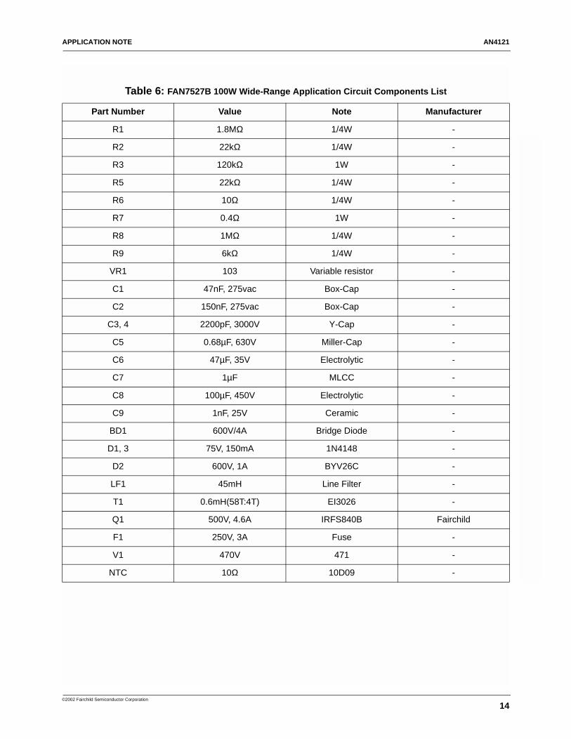
Table 6: FAN7527B 100W Wide-Range Application Circuit Components List
Part Number Value Note Manufacturer
R1 1.8MΩ 1/4W -
R2 22kΩ 1/4W -
R3 120kΩ 1W -
R5 22kΩ 1/4W -
R6 10Ω 1/4W -
R7 0.4Ω 1W -
R8 1MΩ 1/4W -
R9 6kΩ 1/4W -
VR1 103 Variable resistor -
C1 47nF, 275vac Box-Cap -
C2 150nF, 275vac Box-Cap -
C3, 4 2200pF, 3000V Y-Cap -
C5 0.68µF, 630V Miller-Cap -
C6 47µF, 35V Electrolytic -
C7 1µF MLCC -
C8 100µF, 450V Electrolytic -
C9 1nF, 25V Ceramic -
BD1 600V/4A Bridge Diode -
D1, 3 75V, 150mA 1N4148 -
D2 600V, 1A BYV26C -
LF1 45mH Line Filter -
T1 0.6mH(58T:4T) EI3026 -
Q1 500V, 4.6A IRFS840B Fairchild
F1 250V, 3A Fuse -
V1 470V 471 -
NTC 10Ω 10D09 -

APPLICATION NOTE AN4121
15
©2002 Fairchild Semiconductor Corporation
Table 7: FAN7527B 100W 220Vac Application Circuit Components List
Part Number Value Note Manufacturer
R1 1.8MΩ 1/4W -
R2 18kΩ 1/4W -
R3 120kΩ 1W -
R5 22kΩ 1/4W -
R6 10Ω 1/4W -
R7 0.8Ω 1W -
R8 1MΩ 1/4W -
R9 6kΩ 1/4W -
VR1 103 Variable resistor -
C1 47nF, 275vac Box-Cap -
C2 150nF, 275vac Box-Cap -
C3, 4 2200pF, 3000V Y-Cap -
C5 0.47µF, 630V Miller-Cap -
C6 47µF, 35V Electrolytic -
C7 1µF MLCC -
C8 100µF, 450V Electrolytic -
C9 1nF, 25V Ceramic -
BD1 600V/4A Bridge Diode -
D1, 3 75V, 150mA 1N4148 -
D2 600V, 1A BYV26C -
LF1 45mH Line Filter -
T1 0.8mH(75T:5T) EI2820 -
Q1 500V, 4.6A IRFS840B Fairchild
F1 250V, 3A Fuse -
V1 470V 471 -
NTC 10Ω 10D09 -

APPLICATION NOTE AN4121
16
©2002 Fairchild Semiconductor Corporation
Table 8: FAN7527B 150W Wide-Range Application Circuit Components List
Part Number Value Note Manufacturer
R1 1.8MΩ 1/4W -
R2 22kΩ 1/4W -
R3 120kΩ 1W -
R5 22kΩ 1/4W -
R6 10Ω 1/4W -
R7 0.25Ω 1W -
R8 1MΩ 1/4W -
R9 6kΩ 1/4W -
VR1 103 Variable resistor -
C1 330nF, 275vac Box-Cap -
C2 330nF, 275vac Box-Cap -
C3, 4 2200pF, 3000V Y-Cap -
C5 1µF, 630V Miller-Cap -
C6 47µF, 35V Electrolytic -
C7 1µF MLCC -
C8 150µF, 450V Electrolytic -
C9 1nF, 25V Ceramic -
BD1 600V/6A Bridge Diode -
D1, 3 75V, 150mA 1N4148 -
D2 600V, 1.5A SUF15J -
LF1 45mH Line Filter -
T1 0.495mH(54T:4T) EI4035 -
Q1 500V, 13.4A FQA13N50 Fairchild
F1 250V, 3A Fuse -
V1 470V 471 -
NTC 10Ω 10D09 -

AN4121 APPLICATION NOTE
17
©2002 Fairchild Semiconductor Corporation
Table 9: FAN7527B 150W 220Vac Application Circuit Components List
Part Number Value Note Manufacturer
R1 1.8MΩ 1/4W -
R2 22kΩ 1/4W -
R3 120kΩ 1W -
R5 22kΩ 1/4W -
R6 10Ω 1/4W -
R7 0.5Ω 1W -
R8 1MΩ 1/4W -
R9 6kΩ 1/4W -
VR1 103 Variable resistor -
C1 330nF, 275vac Box-Cap -
C2 330nF, 275vac Box-Cap -
C3, 4 2200pF, 3000V Y-Cap -
C5 1µF, 630V Miller-Cap -
C6 47µF, 35V Electrolytic -
C7 1µF MLCC -
C8 150µF, 450V Electrolytic -
C9 1nF, 25V Ceramic -
BD1 600V/6A Bridge Diode -
D1, 3 75V, 150mA 1N4148 -
D2 600V, 1A BYV26C -
LF1 45mH Line Filter -
T1 0.56mH(46T:3T) EI3026 -
Q1 500V, 5.3A FQPF9N50 Fairchild
F1 250V, 3A Fuse -
V1 470V 471 -
NTC 10Ω 10D09 -

AN4121 APPLICATION NOTE
18
©2002 Fairchild Semiconductor Corporation
Table 10: FAN7527B 200W Wide-Range Application Circuit Components List
Part Number Value Note Manufacturer
R1 2.2MΩ 1/4W -
R2 27kΩ 1/4W -
R3 120kΩ 1W -
R5 22kΩ 1/4W -
R6 10Ω 1/4W -
R7 0.15Ω 1W -
R8 1MΩ 1/4W -
R9 6kΩ 1/4W -
VR1 103 Variable resistor -
C1 330nF, 275vac Box-Cap -
C2 330nF, 275vac Box-Cap -
C3, 4 2200pF, 3000V Y-Cap -
C5 1µF, 630V Miller-Cap -
C6 47µF, 35V Electrolytic -
C7 1µF MLCC -
C8 220µF, 450V Electrolytic -
C9 1nF, 25V Ceramic -
BD1 600V/6A Bridge Diode -
D1, 3 75V, 150mA 1N4148 -
D2 600V, 1.5A SUF15J -
LF1 45mH Line Filter -
T1 0.4mH(76T:5T) CM330060(troidal core) ChangSung
Q1 500V, 13.4A FQA13N50 Fairchild
F1 250V, 3A Fuse -
V1 470V 471 -
NTC 10Ω 10D09 -

APPLICATION NOTE AN4121
19
©2002 Fairchild Semiconductor Corporation
Table 11: FAN7527B 200W 220Vac Application Circuit Components List
Part Number Value Note Manufacturer
R1 2.2MΩ 1/4W -
R2 22kΩ 1/4W -
R3 120kΩ 1W -
R5 22kΩ 1/4W -
R6 10Ω 1/4W -
R7 0.4Ω 1W -
R8 1MΩ 1/4W -
R9 6kΩ 1/4W -
VR1 103 Variable resistor -
C1 330nF, 275vac Box-Cap -
C2 330nF, 275vac Box-Cap -
C3, 4 2200pF, 3000V Y-Cap -
C5 1µF, 630V Miller-Cap -
C6 47µF, 35V Electrolytic -
C7 1µF MLCC -
C8 220µF, 450V Electrolytic -
C9 1nF, 25V Ceramic -
BD1 600V/6A Bridge Diode -
D1, 3 75V, 150mA 1N4148 -
D2 600V, 1.5A SUF15J -
LF1 45mH Line Filter -
T1 0.4mH(52T:4T) EI3530 -
Q1 500V, 13.4A FQA13N50 Fairchild
F1 250V, 3A Fuse -
V1 470V 471 -
NTC 10Ω 10D09 -

AN4121 APPLICATION NOTE
20
©2002 Fairchild Semiconductor Corporation
NomenclatureIL(peak) (t) : inductor current peak value during one switching cycle
IL(peak) : inductor current peak value during one AC line cycle
IL(peak_max) : maximum inductor current peak value
IL (t) : inductor current
ID : boost diode current
Iin (t) : input current
Iin (peak) : input current peak value
Iin (peak_max) : maximum of the input current peak value
Iin (rms) : input current RMS value
IQrms : MOSFET rms current
IDrms : diode rms current
IDavg : diode average current
IO : output current
IO (max) : maximum output current
Vin (t) : input voltage
∆Vin (max) : maximum input voltage ripple
Vin (peak) : input voltage peak value
Vin (peak_max) : maximum input voltage peak value
Vin (peak_min) : minimum input voltage peak value
Vin (rms) : input voltage RMS value
Vin (rms_max) : maximum input voltage RMS value
Vin (rms_min) : minimum input voltage RMS value
Vin (LL) : low line rms input voltage
Vin (HL) : high line rms input voltage
VO : output voltage
∆VO (max) : maximum output voltage ripple
∆VOVP : maximum output over voltage
PO : output power
PO(max) : maximum output power
Pin : input power
η : converter efficiency
ton : switch on time
toff : switch off time
tf : MOSFET current falling time
TS : switching period
fac : AC line frequency
ω : AC line angular frequency
fSW : switching frequency
fSW(max) : maximum switching frequency
fSW(min) : minimum switching frequency
L : boost inductance
CO : output capacitance
Cin : input capacitance
η : converter efficiency
Naux : auxiliary winding turn number
NP : boost inductor turn number
Ccomp : compensation capacitance
Ridet : zero current detection resistance
RST : start-up resistance
R1 : output voltage divider top resistance
R2 : output voltage divider bottom resistance
Rin1 : input voltage divider top resistance
Rin2 : input voltage divider bottom resistance
Rsense : current sense resistance
ISTmax : maximum start-up supply current
CST : start-up capacitance
HY(ST)min : minimum UVLO hysteresis
K : multiplier gain
Gin (min) : minimum input voltage sense gain
Gin (max) : maximum input voltage sense gain

APPLICATION NOTE AN4121
21
©2002 Fairchild Semiconductor Corporation

AN4121 APPLICATION NOTE
5/30/02 0.0m 002Stock#ANxxxxxxxxx
2002 Fairchild Semiconductor Corporation
DISCLAIMER FAIRCHILD SEMICONDUCTOR RESERVES THE RIGHT TO MAKE CHANGES WITHOUT FURTHER NOTICE TO ANY PRODUCTS HEREIN TO IMPROVE RELIABILITY, FUNCTION OR DESIGN. FAIRCHILD DOES NOT ASSUME ANY LIABILITY ARISING OUT OF THE APPLICATION OR USE OF ANY PRODUCT OR CIRCUIT DESCRIBED HEREIN; NEITHER DOES IT CONVEY ANY LICENSE UNDER ITS PATENT RIGHTS, NOR THE RIGHTS OF OTHERS.
LIFE SUPPORT POLICY FAIRCHILD’S PRODUCTS ARE NOT AUTHORIZED FOR USE AS CRITICAL COMPONENTS IN LIFE SUPPORT DEVICES OR SYSTEMS WITHOUT THE EXPRESS WRITTEN APPROVAL OF THE PRESIDENT OF FAIRCHILD SEMICONDUCTOR CORPROATION. As used herein:
1. Life support devices or systems are devices or systems which, (a) are intended for surgical implant into the body, or (b) support or sustain life, or (c) whose failure to perform when properly used in accordance with instructions for use provided in the labeling, can be reasonably expected to result in significant injury to the user.
2. A critical component is any component of a life support device or system whose failure to perform can be reasonably expected to cause the failure of the life support device or system, or to affect its safety or effectiveness.
www.fairchildsemi.com

www.onsemi.com1
ON Semiconductor and are trademarks of Semiconductor Components Industries, LLC dba ON Semiconductor or its subsidiaries in the United States and/or other countries.ON Semiconductor owns the rights to a number of patents, trademarks, copyrights, trade secrets, and other intellectual property. A listing of ON Semiconductor’s product/patentcoverage may be accessed at www.onsemi.com/site/pdf/Patent−Marking.pdf. ON Semiconductor reserves the right to make changes without further notice to any products herein.ON Semiconductor makes no warranty, representation or guarantee regarding the suitability of its products for any particular purpose, nor does ON Semiconductor assume any liabilityarising out of the application or use of any product or circuit, and specifically disclaims any and all liability, including without limitation special, consequential or incidental damages.Buyer is responsible for its products and applications using ON Semiconductor products, including compliance with all laws, regulations and safety requirements or standards,regardless of any support or applications information provided by ON Semiconductor. “Typical” parameters which may be provided in ON Semiconductor data sheets and/orspecifications can and do vary in different applications and actual performance may vary over time. All operating parameters, including “Typicals” must be validated for each customerapplication by customer’s technical experts. ON Semiconductor does not convey any license under its patent rights nor the rights of others. ON Semiconductor products are notdesigned, intended, or authorized for use as a critical component in life support systems or any FDA Class 3 medical devices or medical devices with a same or similar classificationin a foreign jurisdiction or any devices intended for implantation in the human body. Should Buyer purchase or use ON Semiconductor products for any such unintended or unauthorizedapplication, Buyer shall indemnify and hold ON Semiconductor and its officers, employees, subsidiaries, affiliates, and distributors harmless against all claims, costs, damages, andexpenses, and reasonable attorney fees arising out of, directly or indirectly, any claim of personal injury or death associated with such unintended or unauthorized use, even if suchclaim alleges that ON Semiconductor was negligent regarding the design or manufacture of the part. ON Semiconductor is an Equal Opportunity/Affirmative Action Employer. Thisliterature is subject to all applicable copyright laws and is not for resale in any manner.
PUBLICATION ORDERING INFORMATIONN. American Technical Support: 800−282−9855 Toll FreeUSA/Canada
Europe, Middle East and Africa Technical Support:Phone: 421 33 790 2910
Japan Customer Focus CenterPhone: 81−3−5817−1050
www.onsemi.com
LITERATURE FULFILLMENT:Literature Distribution Center for ON Semiconductor19521 E. 32nd Pkwy, Aurora, Colorado 80011 USAPhone: 303−675−2175 or 800−344−3860 Toll Free USA/CanadaFax: 303−675−2176 or 800−344−3867 Toll Free USA/CanadaEmail: [email protected]
ON Semiconductor Website: www.onsemi.com
Order Literature: http://www.onsemi.com/orderlit
For additional information, please contact your localSales Representative
© Semiconductor Components Industries, LLC