design of robust energy-efficient digital...
TRANSCRIPT

DESIGN OF ROBUST ENERGY-EFFICIENT DIGITAL CIRCUITS
USING GEOMETRIC PROGRAMMING
A DISSERTATION
SUBMITTED TO THE DEPARTMENT OF ELECTRICAL
ENGINEERING
AND THE COMMITTEE ON GRADUATE STUDIES
OF STANFORD UNIVERSITY
IN PARTIAL FULFILLMENT OF THE REQUIREMENTS
FOR THE DEGREE OF
DOCTOR OF PHILOSOPHY
Dinesh Patil
March 2008

c© Copyright by Dinesh Patil 2008
All Rights Reserved
ii

I certify that I have read this dissertation and that, in my opinion, it is fully
adequate in scope and quality as a dissertation for the degree of Doctor of
Philosophy.
(Mark Horowitz) Principal Adviser
I certify that I have read this dissertation and that, in my opinion, it is fully
adequate in scope and quality as a dissertation for the degree of Doctor of
Philosophy.
(Stephen Boyd)
I certify that I have read this dissertation and that, in my opinion, it is fully
adequate in scope and quality as a dissertation for the degree of Doctor of
Philosophy.
(S. S. Mohan)
Approved for the University Committee on Graduate Studies.
iii

iv

Abstract
Power dissipation has become a critical design constraint in all digital systems. Designers
must focus on creating energy-efficient circuits to achievethe highest performance within a
specified energy budget or dissipate the lowest energy for a given performance. In addition,
as technology scales, increasing process variations can significantly degrade circuit timing
and power. These variations must be accounted for during design to produce robust circuits
that guarantee a desired performance after fabrication.
This thesis focuses on the automated design of robust energy-efficient digital circuits.
Using device sizes, and supply and threshold voltages as variables, we formulate the energy-
efficient circuit design problem as a Geometric Program. GPsare a special class of convex
optimization problems and can be solved efficiently. We develop analytical models of gate
delay and energy, and include different design scenarios like changing logic styles, dis-
crete threshold voltages, wire resistances and capacitances, signal slope constraints and so
on in the optimization. To facilitate design entry and post-optimization analysis, we have
built the Stanford Circuit Optimization Tool (SCOT). As a design case study we explore
the energy-delay tradeoff of different 32bit adder topologies using SCOT. These tradeoff
curves show that adders with an average fanin of two per stagehaving the fewest logic
stages and smallest wire overhead are most energy-efficient.
Gate delay uncertainties due to process variations cause a spread in the overall circuit
v

delay. We show how deterministic sizing, which optimizes the nominal delay ignoring
process variations, can make the overall delay much worse under variations because it
results into many critical paths that may contain small devices.
To solve this problem, we propose two heuristics that guide the optimizer to create a
solution that comes close to optimizing the performance that guarantees a desired yield.
First, we augment the gate delay models with standard deviation delay margins. Second,
we use a “soft max” function to combine path delays at converging nodes. Using these
heuristics retains the original GP form of deterministic sizing and therefore incurs only a
modest computational overhead. The improvement in robustness over deterministic sizing
depends on the circuit topology and the extent of variationsspecified by the technology.
For a 90nm technology, assuming a 15% standard deviation in the delay of a 1µ wide drive
transistor, results show that using the proposed heuristictechniques of statistical sizing with
the correct statistical estimate of overall energy improves the energy-delay tradeoff curve
by 10% for 32-bit adders.
vi

Acknowledgements
In all these years of my Ph.D., I have gained immensely in knowledge and perspective from
many people. I feel fortunate to have had the opportunity of working with some of the best
people in my field and to have brushed shoulders with some of the brightest students.
First and foremost, I would like to thank my adviser, Prof. Mark Horowitz, who, quite
simply, taught me “how to think”. I am constantly amazed by his depth of understanding
and I am grateful for his patience during all the time I took tounderstand new ideas, get the
big picture and learn habits of effective research. His honest critique has taught me to be
a good reviewer of my own work. I only hope that someday I will come close to his level
of thinking. I also had the privilege of working with Prof. Stephen Boyd, who mentored
me as my co-adviser. Along with his enthusiasm and his valuable insights in optimization,
he taught me the value of consistency and precision in technical writing and presentation
that makes for lucid, beautiful papers. I am very grateful for his excellent teaching and
support throughout my research. I would also like to thank Dr. S. S. Mohan for reviewing
my thesis and inspiring me with his constant smile and industry, both during my internship
at Barcelona Design Inc. and during my thesis writing. I am thankful to Prof. Krishna
Saraswat and Prof. Thomas Lee for many insightful discussions I have had with them.
My incredible research group at Stanford consists of brilliant people from many dif-
ferent technical backgrounds. I have learned a lot from their work habits. I thank my
vii

seniors Ken Mai, Ron Ho, Dean Liu and Vladimir Stojanovic forinitializing me into cir-
cuit design and for their invaluable guidance and tips. Ron continues to be my mentor at
Sun Microsystems. I thank my group-mates Samuel Palermo, Hae-Chang Lee, Elad Alon,
Vicky Wong, Valentin Abramzon, Amir Amirkhany, Bita Nezamfar, Francois Labonte, Jim
Weaver, Alex Solomatnikov, Amin Firoozshahian, Xiling Shen and Omid Azizi, for all
their company and friendship during courses, research projects and out-door trips. I would
also like to thank Sunghee Yun and Seung-Jean Kim from Prof. Boyd’s research group for
their invaluable support and contribution towards my research.
Special thanks are due to Teresa Lynn and Penny Chumley for being great admins and
promptly resolving my administrative issues with amazing ease. I am grateful to MARCO
C2S2 for funding my research and providing a platform for collaborating with the industry.
I would also like to thank Dr. Arash Hassibi, for giving me theopportunity of interning at
Barcelona Design Inc.
Words cannot express my gratitude to all my friends at Stanford. They have enriched
my life with many wonderful thoughts and inspiring ideas. I thank them for making my
stay on campus so enjoyable and memorable. I thank the members of Dhwani, the Indian
music group at Stanford, for the great times I have had playing some beautiful music, and
Pt. Habib Khan, for sharing his knowledge of music with me. I thank Poorvi for her
understanding and support, while I stole time from her to give to my thesis.
Finally, I would like to offer my gratitude to my mom Nisha Patil, my dad Dilip Patil
and my grand parents. Every success of my life is ultimately the consequence of their
relentless efforts to see that I get the best of education. I dedicate this thesis to them.
viii
Contents
Abstract v
Acknowledgements vii
List of Tables xiii
List of Figures xvii
List of Symbols and Acronyms xx
1 Introduction 1
2 Energy, delay and scaling 5
2.1 Modeling CMOS energy and delay . . . . . . . . . . . . . . . . . . . . . .6
2.1.1 CMOS transistor characteristics . . . . . . . . . . . . . . . . .. . 7
2.1.2 Dynamic energy model . . . . . . . . . . . . . . . . . . . . . . . . 10
2.1.3 Leakage energy model . . . . . . . . . . . . . . . . . . . . . . . . 11
2.1.4 Modeling gate delay . . . . . . . . . . . . . . . . . . . . . . . . . 12
2.2 Technology Scaling . . . . . . . . . . . . . . . . . . . . . . . . . . . . . . 18
2.3 Process variability . . . . . . . . . . . . . . . . . . . . . . . . . . . . . .. 21
ix

3 Optimization for energy-efficiency 25
3.1 Digital circuit sizing . . . . . . . . . . . . . . . . . . . . . . . . . . . .. 26
3.2 Optimization framework . . . . . . . . . . . . . . . . . . . . . . . . . . .29
3.2.1 Digital circuit design problem as a Geometric Program. . . . . . . 30
3.2.2 Prior work in performance-energy optimization . . . . .. . . . . . 32
3.3 GP compatible models . . . . . . . . . . . . . . . . . . . . . . . . . . . . 34
3.3.1 Modeling gate delay . . . . . . . . . . . . . . . . . . . . . . . . . 34
3.3.2 Modeling leakage energy . . . . . . . . . . . . . . . . . . . . . . . 35
3.3.3 Stanford Circuit Optimization Tool (SCOT) . . . . . . . . .. . . . 36
3.4 Circuit case study: 32-bit adder . . . . . . . . . . . . . . . . . . . .. . . . 38
3.4.1 Adder topologies . . . . . . . . . . . . . . . . . . . . . . . . . . . 39
3.4.2 Design Constraints . . . . . . . . . . . . . . . . . . . . . . . . . . 43
3.4.3 Results and analysis . . . . . . . . . . . . . . . . . . . . . . . . . 44
3.4.4 Adder design space . . . . . . . . . . . . . . . . . . . . . . . . . . 55
3.5 Summary . . . . . . . . . . . . . . . . . . . . . . . . . . . . . . . . . . . 56
4 Optimization for robustness 59
4.1 Estimating performance bounds . . . . . . . . . . . . . . . . . . . . .. . 61
4.1.1 Performance bounds via stochastic dominance . . . . . . .. . . . 63
4.1.2 Performance bounds via surrogate netlists . . . . . . . . .. . . . . 65
4.1.3 Monte Carlo analysis . . . . . . . . . . . . . . . . . . . . . . . . . 70
4.1.4 Bound estimates for representative circuits . . . . . . .. . . . . . 72
4.2 Effect of ignoring process variations . . . . . . . . . . . . . . .. . . . . . 74
4.3 Exact statistical sizing . . . . . . . . . . . . . . . . . . . . . . . . . .. . . 76
4.3.1 Balance of sensitivities . . . . . . . . . . . . . . . . . . . . . . . .80
4.3.2 Non-scalability of the exact solution . . . . . . . . . . . . .. . . . 83
x

4.3.3 Previous work in robust sizing . . . . . . . . . . . . . . . . . . . .85
4.3.4 Basic idea for robust sizing . . . . . . . . . . . . . . . . . . . . . .86
4.4 Heuristic techniques for robust sizing . . . . . . . . . . . . . .. . . . . . 87
4.4.1 Adding delay margins (ADM) . . . . . . . . . . . . . . . . . . . . 87
4.4.2 Using soft-max (USM) for merging path delays . . . . . . . .. . . 88
4.4.3 Validating USM and ADM with two Gaussian delay variables . . . 90
4.5 Applying robust sizing heuristics . . . . . . . . . . . . . . . . . .. . . . . 91
4.6 Including variations in energy . . . . . . . . . . . . . . . . . . . . .. . . 97
4.7 Summary . . . . . . . . . . . . . . . . . . . . . . . . . . . . . . . . . . . 101
5 Conclusions 103
5.1 Future work . . . . . . . . . . . . . . . . . . . . . . . . . . . . . . . . . . 105
A Geometric programming basics 107
A.1 Monomial and posynomial functions . . . . . . . . . . . . . . . . . .. . . 107
A.2 Standard form Geometric Program . . . . . . . . . . . . . . . . . . . .. . 109
A.2.1 Simple extensions of GP . . . . . . . . . . . . . . . . . . . . . . . 110
A.3 Generalization . . . . . . . . . . . . . . . . . . . . . . . . . . . . . . . . . 111
A.3.1 Generalized geometric program . . . . . . . . . . . . . . . . . . .114
B Stanford Circuit Optimization Tool 117
B.1 Modeling issues in important circuit scenarios . . . . . . .. . . . . . . . . 118
B.1.1 Signal rise/fall time constraints . . . . . . . . . . . . . . . .. . . . 119
B.1.2 Transmission gate circuits . . . . . . . . . . . . . . . . . . . . . .119
B.1.3 Local feedback - keepers . . . . . . . . . . . . . . . . . . . . . . . 120
B.1.4 Pulse width constraints . . . . . . . . . . . . . . . . . . . . . . . . 121
B.1.5 Modeling dual-rail gate delay . . . . . . . . . . . . . . . . . . . .122
xi

B.1.6 Handling discrete variables . . . . . . . . . . . . . . . . . . . . .. 123
Bibliography 125
xii

List of Tables
4.1 Estimates ofQ0.95(Td) on different combinational digital circuits. Delay
values are in FO4. . . . . . . . . . . . . . . . . . . . . . . . . . . . . . . . 73
4.2 SSTA of robust sizing using Pelgrom’s model. Delays are in FO4. The
originalQ0.95(Td) is for deterministic sizing. . . . . . . . . . . . . . . . . 95
4.3 Results of robust sizing techniques in case whereσ ∝ µ. Delays are in FO4. 96
xiii

xiv

List of Figures
1.1 Growing number of digital systems across a wide power-performance range 2
2.1 Forms of energy dissipation in CMOS circuits. The graphsshows the cur-
rents associated with the corresponding energy dissipation. . . . . . . . . . 6
2.2 3D view of the NMOS transistor . . . . . . . . . . . . . . . . . . . . . . .8
2.3 Effect of loading conditions on the accuracy of our additive slope delay model 15
2.4 Delay of a stack of NMOS transistors activated at the intermediate input . . 17
2.5 Step delay model validation for a stack of 2 NMOS transistors . . . . . . . 18
2.6 Scaling oftox, Vdd, Vth with gate length . . . . . . . . . . . . . . . . . . . 20
2.7 Types of process variations . . . . . . . . . . . . . . . . . . . . . . . .. . 22
3.1 Energy-efficiency tradeoff space of a digital circuit block . . . . . . . . . . 25
3.2 Gate delay constraints for the circuit sizing problem . .. . . . . . . . . . . 27
3.3 An example circuit netlist with boundary signals . . . . . .. . . . . . . . . 28
3.4 Modeling the negative exponential ofIleak with a monomial . . . . . . . . . 37
3.5 CPL dot diagram of selected adders with their (R, T, L, F ). Solid lines and
circles are PG signals and PG combine cells, dashed lines anddiamonds are
carry signals and carry generate cells, and empty circles represent wires or
buffers. . . . . . . . . . . . . . . . . . . . . . . . . . . . . . . . . . . . . 40
xv

3.6 E-D curves for the three radix 2 corner adders. . . . . . . . . .. . . . . . . 45
3.7 Change inVdd andVths across the E–D space for a Sklansky adder. . . . . . 46
3.8 Energy consumed in wires. . . . . . . . . . . . . . . . . . . . . . . . . . .48
3.9 Comparison of Sklansky adder E–D curves to its closest neighbors and to
a 2-bit sum select scheme. . . . . . . . . . . . . . . . . . . . . . . . . . . 49
3.10 Comparison of Sklansky domino and dual-rail domino tree adders. . . . . . 50
3.11 Comparison of the linear adder to closest tree adders. The Brent Kung
adder is also shown for reference. . . . . . . . . . . . . . . . . . . . . . .51
3.12 E–D tradeoff curves of 32-bit and 27-bit Sklansky adders of different radices. 54
3.13 Effect of external buffering on radix 2 Sklansky (left)and Brent Kung
(right) adders. . . . . . . . . . . . . . . . . . . . . . . . . . . . . . . . . . 55
3.14 32-bit adder E-D space.Cload = 100fF . . . . . . . . . . . . . . . . . . . 56
4.1 Possible improvement inQ95 E–D curve with design for robustness . . . . 60
4.2 κ required for estimating the upper bound ofQα(Td) . . . . . . . . . . . . 70
4.3 Accuracy of timing bounds to actualQ0.95(Td), normalized to unity . . . . 74
4.4 Monte Carlo analysis on a deterministically sized 32-bit adder . . . . . . . 75
4.5 µ − σ scatter plot for deterministic sizing . . . . . . . . . . . . . . . . . .76
4.6 Example circuit for exact solution of the statistical design problem . . . . . 77
4.7 Modeling inverse CDF with max of 4 monomial terms . . . . . . .. . . . 79
4.8 Comparison of robust design to nominal design . . . . . . . . .. . . . . . 80
4.9 A simple circuit with symmetric structure but differentloads . . . . . . . . 81
4.10 Tradeoff between mean delays for the sameQ0.95(Td) . . . . . . . . . . . 82
4.11 Change in the optimal mean with the ratio of energy between the two chains 83
4.12 A simple circuit with two dependent paths . . . . . . . . . . . .. . . . . . 84
xvi

4.13 Delay PDFs with comparable means but different variances produce long
tails at converging nodes . . . . . . . . . . . . . . . . . . . . . . . . . . . 85
4.14 Validating USM and ADM for the84th percentile point . . . . . . . . . . . 91
4.15 Validating USM and ADM for the95th percentile point . . . . . . . . . . . 92
4.16 Improvement inQ0.95(Td) for a 32-bit LF adder usingκ = 1.5 andp = 30 . 93
4.17 µ–σ scatter plot for all paths of 32bit LF adder (Tpath = path delay) . . . . . 94
4.18 Fleak and normalizedµ(Ij) (4.17) as a function of transistor width . . . . . 99
4.19 Improvement in the energy-delay tradeoff curve for the95th percentile de-
lay due to statistical design . . . . . . . . . . . . . . . . . . . . . . . . . .100
B.1 Block diagram of Stanford Circuit Optimization Tool (SCOT) . . . . . . . 119
B.2 Local feedback in logic circuits: keepers and feedback inverters . . . . . . 121
B.3 Combinational logic block CL with pulse width constraints on a sub-block S 122
B.4 Schematic of the CCC that generates the bit sum for carry=0 in a 2bit sum
select ling adder. Special commands shown on the bottom right are neces-
sary to avoid choosing false transistor paths for delay . . . .. . . . . . . . 123
B.5 Snapping of discrete variables causes sub-optimality .. . . . . . . . . . . 124
xvii

xviii

List of Symbols and Acronyms
Vdd Supply voltage . . . . . . . . . . . . . . . . . . . . . . . . . . . . . . . . . . . . . .. . . . . . . . . . . . . . . 6
Vth Threshold voltage . . . . . . . . . . . . . . . . . . . . . . . . . . . . . . . . . . .. . . . . . . . . . . . . . . 3
VthN NMOS threshold voltage . . . . . . . . . . . . . . . . . . . . . . . . . . . . . . .. . . . . . . . . . . 43
VthP PMOS threshold voltage . . . . . . . . . . . . . . . . . . . . . . . . . . . . . . .. . . . . . . . . . . . 43
tox Gate oxide thickness . . . . . . . . . . . . . . . . . . . . . . . . . . . . . . . . .. . . . . . . . . . . . . 19
vsat Saturation velocity of carriers in silicon . . . . . . . . . . . . . .. . . . . . . . . . . . . . . . 9
Cox Gate oxide capacitance . . . . . . . . . . . . . . . . . . . . . . . . . . . . . . .. . . . . . . . . . . . . . 8
Vod Gate overdrive (Vdd - Vth) . . . . . . . . . . . . . . . . . . . . . . . . . . . . . . . . . . . . . . . . . . . 9
Ec Critical electrical field . . . . . . . . . . . . . . . . . . . . . . . . . . . . .. . . . . . . . . . . . . . . . . 9
Lmin Minimum gate length . . . . . . . . . . . . . . . . . . . . . . . . . . . . . . . . . .. . . . . . . . . . . 16
Id Transistor drive current . . . . . . . . . . . . . . . . . . . . . . . . . . . . .. . . . . . . . . . . . . . . . 6
Idsat Transistor saturation current . . . . . . . . . . . . . . . . . . . . . . . .. . . . . . . . . . . . . . . . .8
Ileak Leakage current . . . . . . . . . . . . . . . . . . . . . . . . . . . . . . . . . . . . .. . . . . . . . . . . . . . .6
SEC Single Error Correction . . . . . . . . . . . . . . . . . . . . . . . . . . . . . .. . . . . . . . . . . . . . 73
DED Double Error Detection . . . . . . . . . . . . . . . . . . . . . . . . . . . . . . .. . . . . . . . . . . . . 73
xix

xx

Chapter 1
Introduction
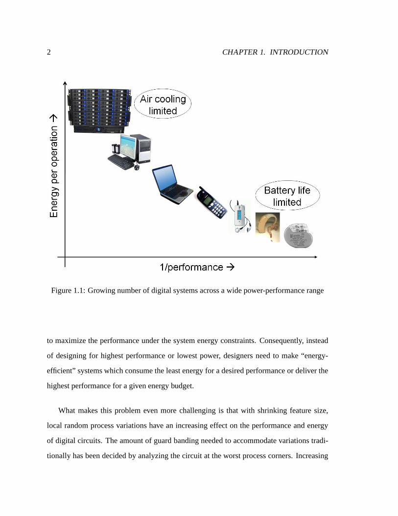
For the past three decades, technology scaling has enabled us to develop faster, smaller,
cheaper logic gates [60], leading to their use in many systems spanning a wide range of
power and performance. Figure 1.1 shows a few example systems starting from the very
low power battery operated devices like hearing aids and pacemakers on the lower right
to high-power high-performance servers and mainframes on the upper left. The power
consumption of a pacemaker is around10µW [97], while modern high end processors
dissipate around 100W [57, 50]. Even though the power consumption of these systems
differ by over 6 orders of magnitude, energy-efficiency is a crucial factor in all of them. In
portable devices, power dissipation directly affects the battery life, therefore these systems
have to minimize their energy consumption while deliveringthe required performance. For
high performance devices, maximum energy dissipation is constrained by power delivery
and cooling system costs. Not only has it become increasingly difficult to supply the high
currents needed by high-end microprocessors, the cost effective air cooling limit, which sits
at around 100W, means that to increase the performance, we need to decrease the energy per
operation to keep the chip power dissipation within this limit. The goal in these systems is
1
2 CHAPTER 1. INTRODUCTION
Figure 1.1: Growing number of digital systems across a wide power-performance range
to maximize the performance under the system energy constraints. Consequently, instead
of designing for highest performance or lowest power, designers need to make “energy-
efficient” systems which consume the least energy for a desired performance or deliver the
highest performance for a given energy budget.
What makes this problem even more challenging is that with shrinking feature size,
local random process variations have an increasing effect on the performance and energy
of digital circuits. The amount of guard banding needed to accommodate variations tradi-
tionally has been decided by analyzing the circuit at the worst process corners. Increasing

3
local random variability means that our current method of guard banding can give very pes-
simistic values for the guard band. Since it does not consider the averaging effect of these
variations, it causes the circuit to be over-designed, which adversely affects its energy-
efficiency. Process variations hurt in many other ways as well. The exponential dependence
of leakage energy onVth causes the overall average leakage energy to increase significantly
with Vth variation. Thus in designing for the highest performance point without respecting
Vth variability, the leakage for most fabricated chips will be unacceptable, wasting a lot of
energy. To minimize this loss of energy-efficiency during fabrication, design optimization
must account for process variations.
Robust energy-efficient design can be done at many levels of system design hierarchy
– problem formulation, architecture, circuits and devices. This thesis focuses on robust
energy-efficient circuit design. The design variables are circuit topology, logic style, tran-
sistor sizes, and supply and threshold voltages. The designmetrics are the specified perfor-
mance and energy, while the boundary constraints include input signal arrival times, output
loads and signal transition times. We formulate the digitalcircuit design optimization prob-
lem as aGeometricProgram (Appendix A). A GP is a special type of convex optimization
problem which can be efficiently solved using interior pointmethods [10]. To facilitate de-
sign entry and analysis, we created SCOT – the Stanford Circuit Optimization Tool, which
was useful for creating optimized designs using Geometric Programming. We analytically
model the energy and delay of digital circuit blocks as GP compatible mathematical func-
tions of the design variables. Using this tool, we have investigated the energy-efficiency
of different adder topologies and extracted the overall energy-delay tradeoff curve of 32bit
adders. Such energy-delay tradeoff curves can be used at upper levels in the design hierar-
chy to create energy-efficient architectures.
To make the design robust against random process variations, models for saturation
4 CHAPTER 1. INTRODUCTION
and leakage current variation are incorporated in the design optimizer itself. While doing
this exactly can be difficult, we have developed efficient heuristics to guide the optimizer
in choosing appropriate values of the design variables, with a modest overhead in design
time. Depending on the topology, the resulting designs can be significantly more robust to
the process variations than the nominal designs.
Chapter 2 describes the aspects of CMOS technology scaling that cause the two big
issues we face today – power dissipation and process variability. Next, Chapter 3 looks at
the power dissipation problem without considering variations. It describes our formulation
of the energy-efficient digital circuit design problem using analytical energy and delay
models and uses these models to do a case-study using a 32-bitadder to show how the
optimization framework works. Although circuits designedthis way are energy-efficient,
they are not optimal in the face of process variations. Chapter 4 starts by describing ways
of analyzing circuit timing with uncertain gate delays. We show the negative effect of of
process variations on otherwise optimally designed digital circuits. With this motivation
we discuss efficient techniques to include process variability in the design optimizer to
generate statistically robust circuits.

Chapter 2
Energy, delay and scaling
Power is now a critical issue for integrated circuit designers. Before describing methods
of addressing this issue by creating energy efficient designs, this chapter will look at the
basic mechanisms that cause energy dissipation and delay inCMOS circuits. We will then
create simple, but accurate models that will allow us to estimate these quantities for arbi-
trary CMOS gates, and use these models to explain why power has increased during the
past 30 years of scaling, and why the power problem has gottenmuch worse recently. Next
we turn our attention to another factor that affects energy-efficiency – process variabil-
ity. Given that devices have manufacturing tolerances, we need to add margins to ensure
that the manufactured designs meet spec. This has traditionally been done using “corner
files” information about the worst-case points in the manufacturing flow. With technology
scaling, local fluctuations across a single die have become more critical. This chapter ex-
plains why these on-die variations are critical, and how they affect the design optimization
problem.
5

6 CHAPTER 2. ENERGY, DELAY AND SCALING
2.1 Modeling CMOS energy and delay
There are three main sources of energy dissipation in CMOS circuits as shown in Figure
2.1.
10
time timetime
(a) Charging current (b) Short circuit current (c) Leakage current
VddVddVdd
gnd
gndgndgnd
Id
I d
IscI s
c
I lea
k
Ileak
CloadCloadCload
Q = CloadVdd
Figure 2.1: Forms of energy dissipation in CMOS circuits. The graphs shows the currentsassociated with the corresponding energy dissipation.
1. Dynamic energyconsists of the energy dissipated in charging and discharging gate,
diffusion and wire capacitances while switching a signal.
2. Signal transitions are never instantaneous. Whenever a gate switches, the pull up
and pull down devices may be simultaneously on for a brief period until the input
transition is complete, causing short circuit crow-bar current to flow between the
power rails. The energy dissipated in this way during signaltransition forms the
Crow-bar energy.

2.1. MODELING CMOS ENERGY AND DELAY 7
3. A static source-drain leakage current flows through a transistor even when the tran-
sistor is off, i.e. when the gate source voltageVgs is well belowVth. Energy dissipated
statically due to this sub-threshold conduction constitutes theLeakage energy.
The total energy dissipation is the sum of all these components over all gates and wires in
the netlist.
Modeling circuit delay is slightly more difficult as it is determined by the slowest sig-
nal path during each clock cycle. As a digital signal propagates through the circuit, it turns
some transistors on and others off. These transistors then drive their output nodes, charg-
ing and discharging different capacitances and changing the state of other transistors which
drive the next output nodes. The delay of a path of logic is thesum of signal transition
delays through the transistor stages along the path. As delay at every stage consists of
charging or discharging a load capacitanceC to or from voltageV using the driving tran-
sistor’s drain currentI, the delay per stage can be written askCV/I, wherek is a constant.
The drive currentI and the gate capacitance of a transistor are both directly proportional
to the its width. Consequently, if the load capacitanceC is a fixed multiple of the driving
transistor’s gate capacitance, thekCV/I delay becomes independent of transistor sizing. It
depends only on the intrinsic driving properties of the devices in the technology. Therefore,
kCV/I delay measured in this way is a good metric for defining the speed of a technology.
2.1.1 CMOS transistor characteristics
In order to correctly model the transistor currentI, it is important to understand the CMOS
transistor behavior and include in the device model all the important factors that affect
delay and energy of CMOS circuits. Figure 2.2 shows a 3D view of a typical NMOS device
structure that has been scaled over the years. For transistors with long channel length, the
lateral source-drain electric field is small and the channelcarrier velocityν is proportional

8 CHAPTER 2. ENERGY, DELAY AND SCALING
Figure 2.2: 3D view of the NMOS transistor
to the channel electric fieldE.
ν = µE,
whereµ is the mobility, which is largely constant over the operating range. In this scenario,
the drain current in saturationIdsat for a transistor of widthW and lengthL can be modeled
quite accurately by the simple quadratic formula [72]
Idsat =W
2LµCoxV
2od, (2.1)
2.1. MODELING CMOS ENERGY AND DELAY 9
whereVod is the overdrive voltage given byVod = (Vdd − Vth)1 . BecauseIdsat for a
transistor depends only on theW/L ratio, the drive current for a cluster of transistors can
be found easily by modeling each one of them as resistors [34](where the resistance is
proportional toL/W ) and finding the effective resistance of the cluster using the series-
parallel formula for resistors. For example, the current through a stack of two devices can
be modeled as
Idsat ∝1
L1
W1+ L2
W2
,
while for parallel devices we can write
Idsat ∝ W1/L1 + W2/L2.
However, all modern transistors exhibit the so called “highfield effects” which make this
simple modeling very inaccurate. AsL is reduced the lateral field increases and the rela-
tionship between the carrier velocity and electric field starts to saturate [88]. Carriers are
velocity saturated to avsat of around107cm/s in silicon. With short channels, the drain
depletion region forms a larger part of the channel length and voltage on the drain also can
lead to changing the barrier to inversion, thus affecting the Vth. This effect is known as
Drain Induced Barrier Lowering or DIBL [88, 65]. Finally, the low-lateral-field mobility is
affected by the vertical gate field [82]. We use the Meyer saturation current model [89] to
effectively capture all these important effects.
In this model,Idsat of a MOS transistor is given by
Idsat =WvsatCoxV
2od
Vod + EcL, (2.2)
wherevsat is the saturation velocity andEc is the critical lateral electric field that sets the
1As we are talking about digital circuits with rail to rail signal transitions, we useVdd as ourVgs.

10 CHAPTER 2. ENERGY, DELAY AND SCALING
onset of velocity saturation.
Ec =2vsat
µeff
.
Here, the effective mobilityµeff , is itself a function ofVdd andVth as it depends on the
vertical electric field [89]. The magnitude ofEcL relative toVod determines the extent of
velocity saturation and therefore the short channel behavior. WhenEcL >> Vod, the lateral
field is small, so velocity saturation is small andIdsat obeys the square law relationship.
The influence of a strong horizontal field in short channel transistors keeps the device in
saturation well beyond the(Vgs − Vth) level of the long channel device. With velocity
saturation, the drain saturation voltage is given by [89]
Vdsat =(Vgs − Vth)EcL
(Vgs − Vth) + EcL.
For devices below 130nm, this is much lower than(Vdd−Vth) as devices remain in velocity
saturated mode for a substantial portion of their drain voltage swing.
2.1.2 Dynamic energy model
As inputs to a logic circuit change, signals at different nets transition to new values, charg-
ing and discharging the corresponding capacitances. If a capacitanceC swings by a voltage
Vswing through a supply ofVdd, the total energy spent by the supply is the product of the
charge placed on the capacitor and the supply voltage, givenasCVswingVdd. Usually, the
circuit swings are equal toVdd, therefore average total dynamic energy per operation can
be calculated as a sum of the dynamic energy dissipated at each of then nets in the circuit.
Edyn = V 2dd
n∑
i=1
αiCi (2.3)

2.1. MODELING CMOS ENERGY AND DELAY 11
Here, Ci is the sum of the wire capacitance, gate capacitance of the fan-out gates and
parasitic capacitance of the driving transistor stage on net i. The switching activity factor
αi measures the average transition frequency of neti. For a given transition frequency at
the inputs,αi is calculated by fast logical switch level simulation of thecircuit.
Crow-bar current also only occurs during transitions and isgenerally lumped in with
the dynamic power. While it depends on rate of change of the input, it usually is a small
fraction of the dynamic energy and causes a small error if ignored in energy estimation.
The accuracy of the energy model really lies in estimating the different device and wire
capacitances accurately. The MOS gate and diffusion capacitances depend on the applied
voltage. However, for a rail to rail switching transition, the average capacitance gives a
good estimate for power calculation.
2.1.3 Leakage energy model
The current model explained in Section 2.1.1 predicts that there is no drain current when
Vod ≤ 0. However, CMOS transistors do have leakage currents when they are “switched
off”. CMOS gates leak all the time as this leakage current flows through the switched off
transistors. The leakage energy per cycle is the sum of the energy in all the gates in a
circuit.
Eleak = VddTcycle
m∑
i=1
Igate,i (2.4)
Here,m is the number of gates,Igate,i is the weighted sum of the leakage currents of the
gatei over its various logic states andTcycle is the clock cycle time.
Igate,i =∑
j
pjIj(Vdd, Vth,j), (2.5)
12 CHAPTER 2. ENERGY, DELAY AND SCALING
wherepj is the probability of statej andIj is the leakage current in that state, which de-
pends on the width andVth of leaking transistors. Leakage current reduces significantly
with stacking [39], so we consider only those logic states that have a single leaking tran-
sistor between the power rails. The leakage in a gate is distributed between its pull-up
and pull-down stacks according to the proportion of time theother stack is active. In other
words, it depends on the average time the output remains in state 0 or 1 respectively. This is
calculated by measuring the duty factor simultaneously with the switching activity factors
to obtain a good first order estimate ofpj. For a single leaking transistor of widthW , Ij
can be modeled as [63]:
Ij = I0W exp(−(Vth,j − γDVdd)
nbfVT
) (2.6)
whereI0 is a constant,γD is the DIBL coefficient,VT is the thermal voltage equal to
kBT/q, kB being the Boltzman constant andnbf accounts for the body-factor describing
the efficiency of gate to channel coupling [88]. The magnitude by whichVth must change to
cause an order of magnitude change inIj is called sub-threshold slope and can be calculated
asln(10)nbfVT. For most CMOS devices, this value is around 80-100mV/decade.
2.1.4 Modeling gate delay
We have extended the Meyer velocity saturated current model[15, 89] for a transistor to
obtain the delay of CMOS gates. To calculate this delay correctly, it is necessary to consider
the entire path from the power rails to the charging load. Thus for modeling the delay of a
transistor stage we define a stage (gate) as a Channel Connected Component (CCC) [21, 12]
where inputs are only connected to gate terminals. A CCC is defined as the largest group

2.1. MODELING CMOS ENERGY AND DELAY 13
of transistors having their source/drain terminals connected through conducting channels2.
Most common logic gates like inverter, NAND and NOR gates fall in this category. As we
shall see below, tearing circuits into CCCs makes it possible to model the delay of CMOS
gates analytically.
For sake of explanation, we will consider the process of a load capacitance being dis-
charged by an NMOS pull-down stack. The analysis for PMOS pull-up is similar. The fall
delay for discharging a load capacitanceCload to Vdd/2 by applying a rising step input to
the driver NMOS transistor is given by
τstep =CloadVdd
2Id,
where the discharging currentId is given by Equation 2.2. However this model greatly
underestimates the delay in real circuits because of two reasons. Firstly, the input is never
a step but has a finite rise and fall time. This turns on the driver transistor slowly and
contributes to the stage delay. Usually the stage delays arecomparable, so the output does
not crossVswing/2 until the input is well beyond theVdd/2 point. In such cases the input
slope just adds a simple delay term [35]. With this assumption, we can estimate the fall
delayτd by
τd =CloadVdd
2Id+ f(τin), (2.7)
whereτin is the input transition time andf(τin) is the added delay. By approximating
the shape of input transition and the driver current build upas linear, an input with finite
transition time can be considered as a delayed step. This delay,f(τin) is given as [35]
f(τin) = 0.5Vth
Vdd
τin.
2Some transistors are connected to power rails (supply and ground)

14 CHAPTER 2. ENERGY, DELAY AND SCALING
To assess the accuracy of this model, consider a two inverterdelay path driven by a step
input and driving a fixed load. The size of the second stage is fixed while the size of the
first is changed to present inputs with different transitiontimes to the second stage. Figure
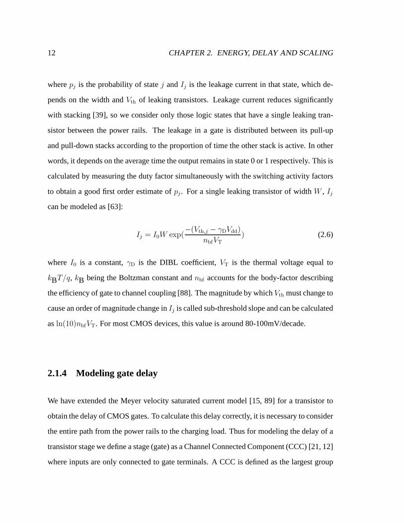
2.3(a) shows the relative error in the estimating the extra delay added to the second due to
its non-zero input transition time. The X axis represents the delay of the first stage relative
to that of the second stage. If the input to the second stage transitions relatively quickly
(i.e. the delay of the first stage is relatively small), the error is less, while for very slowly
changing inputs, the error is large. However, if we measure the delay of the entire path, we
can see that the error in estimating the total delay due to non-zero input transition time is
significantly reduced.
While this error may still be important in timing “analysis”, we care about how it af-
fects optimal “design”. Usually, optimal sizing ensures that stage delays and therefore the
input and output transition times, are comparable. A light loading condition can occur dur-
ing sizing if the transistors in a lightly loaded side path hit their minimum size constraint
while the critical path is heavily loaded. However, in such cases the delay of the entire side
path itself is already small compared to the critical path delay and so does not affect the
sizing. In addition, we constrain the delay of every stage toavoid slowly changing signals
for signal integrity reasons. This reduces the error in delay estimation. The second issue
in accurate delay modeling is that during switching, the gate and drain voltages of the tran-
sistor are changing simultaneously and because of DIBL,Vth is also changing. Therefore
the discharging current is actually changing throughout the output transition andId should
represents an average discharging current. Hence for improved accuracy, we modified the
expression ofIdsat in Equation 2.2 by adding two additional fitting parametersa andb to
give
Id = aWvsatCox(bVdd − Vth)
2
(bVdd − Vth) + EcL.
2.1. MODELING CMOS ENERGY AND DELAY 15
0.3 1 5−20
0
20
40
60
80
100
120
relative stage delay
%er
ror
inad
diti
on
ald
elay
(a) Error in slope effect
0.3 1 5−5
0
5
10
15
20
relative stage delay
%er
ror
into
tald
elay
(b) Error in total delay
Figure 2.3: Effect of loading conditions on the accuracy of our additive slope delay model
Parametera is the averaging coefficient andb accounts for DIBL3 As we are optimizing
for Vdd andVth, we choose these parameters to best fit the entire range of desirableVdd and
Vth.
The above equations can easily model the delay of an inverter, but complex gates are
made of multiple series and parallel stacks of transistors.To model their delay we need
to model the current of a stack of transistors. As was alreadymentioned, modern devices
are velocity saturated and so cannot be combined as resistors. The issue is clear from
Equation 2.2. Unlike the long channel transistor, increasingL of a velocity saturated device
does not reduce the current proportionately. Therefore, a stack of two identical transistors
behaves like a transistor with the same width but twice the length, as opposed to a transistor
with same length with half the width as is true in quadratic transistors. This can be easily
accounted for if all devices in the stack are of equal width, because then we can model that
as a long transistor with the same width. However, in custom design, transistors in a stack
can have different sizes depending on the delay at their gateinputs. For such cases, the
3The values ofa andb used for our 90nm technology are respectively 0.9 and 1.12 for PMOS and 0.7 and1.1 for NMOS.

16 CHAPTER 2. ENERGY, DELAY AND SCALING
current model needs to be generalized to estimate the drive current of a stack of transistors
with unequal widths. The velocity saturated flow of carriersin a stack of transistors can be
thought of as water flowing under pressure in connected pipesof different diameters. Here
the flow of water is restricted mostly by the thinnest pipe, while the length of a thicker
pipe has a relatively small effect on the flow rate. Using thisidea, we model a stack ofn
transistors as an equivalent transistor with an effective width Weff and effective lengthLeff
given as
Weff = min(W1, . . . , Wn),
Leff = Weff
n∑
i=1
Li/Wi,
whereWi andLi are the width and length of theith series transistor. As devices in a digital
circuit are usually of minimum lengthLmin , we can rewriteLeff as
Leff = LminWeff
n∑
i=1
1/Wi.
Thus the equivalent width is set by the most velocity saturated device and the length is set
by the averaged length of all transistors weighted by their widths. This allows us to size
different transistors in the stack. If all widths are equal,the equations result in an equivalent
transistor with the same width and lengthnLmin as expected.
The delay of a stack also consists of discharging4 the intermediate capacitances. If the
switching input is at the bottom of the chain (closer to powerrails), then it has to discharge
all the intermediate nodes. In this case we decompose the fall delay as a sum of fall delays
where each intermediate capacitor is discharged by the chain below it, similar to the Elmore
4charging for PMOS

2.1. MODELING CMOS ENERGY AND DELAY 17
[23] delay calculation as shown in Figure 2.4. Note that the capacitors that are in the same
gnd
gndgnd
gnd
gnd
Cpar1Cpar1
Cpar2
= +
CloadCload
Figure 2.4: Delay of a stack of NMOS transistors activated atthe intermediate input
state before and after the transition are not included in calculating the delay. Therefore we
have no term for capacitorC3 in the figure.
Figure 2.5 shows the validation of our model against spice simulations for step input to
a stack of two NMOS devices as in a NAND gate. Let the width of the NMOS closer to
the output beW1 and the width of NMOS closer to ground beW2. The models are more
accurate near the point whereW1 = W2. The error in the estimate shown in Figure 2.5(a)
is due to our assumption that the intermediate node is atVdd prior to discharge. In Figure
2.5(b), the error in modeling the delay from top transistor switching comes mainly due to
ignoring charge build up in the capacitor at the intermediate node during the transition.
If the intermediate capacitor is relatively large for the bottom transistor (widthW2) and
comparable to the load capacitance, it can act as a virtual ground causing a smaller delay5
and longer transition tail for the output [34].
An interesting effect of velocity saturation is that asVdd is reduced, the relative reduc-
tion in the current of a stack of transistors is higher than that of a single transistor. This
is expected because with reducingVdd, the single transistor is less velocity saturated and
therefore has a larger current relative to the stack of transistors, which suffered less velocity
5as calculated as the delay between the input reaching half-swing to output reaching half-swing

18 CHAPTER 2. ENERGY, DELAY AND SCALING
0.2 1 55
10
15
20
25
30
35
40
W2/W1 (log scale)
del
ayin
ps
Spicemodel
(a) Bottom transistor switching
0.2 1 55
10
15
20
25
30
W2/W1 (log scale)
del
ayin
ps
Spicemodel
(b) Top transistor switching
Figure 2.5: Step delay model validation for a stack of 2 NMOS transistors
saturation to begin with. This is important for sizing, as itmeans that for the same drive
capability, a stack of transistors (as in a NAND or NOR gate) has to be sized bigger rela-
tive to the single transistor stage (as in an inverter) asVdd is reduced. This effect is neatly
captured by the(Vod + EcLeff ) term of the drive current model.
The accuracy of the delay model remains well within 10% for chains of up to four tran-
sistors for reasonableCload and intermediate parasitic capacitors and input signal transition
times (τin) are comparable to the output signal transition times. Structures with up to four
transistor stack include almost all the usual CMOS logic gates. In larger gates where there
are many parallel stacks of transistors connected to the output, the model may underesti-
mate the overall delay of a particular transistor stack as itdoes not consider the intermediate
parasitic capacitance from other partially turned on stacks.
2.2 Technology Scaling
Over the years, the IC industry has successfully implemented Dennard scaling to improve
performance. In 1974 Dennard proposed constant field scaling [19], where the electric
fields in a MOS device are kept constant by scaling voltages with lithographic dimensions.
2.2. TECHNOLOGY SCALING 19
Scaling the feature size by the scaling factorα (α ≈ 0.7) per generation improved the delay
per switching event by1/α. The gate capacitance per micron remained constant as both
the device lengthL and the oxide thicknesstox scaled byα. The device current per micron
also remained constant because the scaling ofL andtox was offset by the scaling ofVdd and
Vth. This follows from Equation 2.1. This trend continued even in the velocity saturated
device regime as can be observed by implementing scaling in Equation 2.2. Consequently,
the CV/I figure improved by1/α in every generation. This improvement in switching
delay enabled a1/α increase in the clock frequencyfclk. Improved circuit techniques like
deeper pipelining allowedfclk to be increased further. With the gate capacitance per unit
areaCarea increasing by1/α due to scaling oftox, the dynamic energy per switching event
per unit area given asCareaV2 decreased by1/α. Combined with slightly greater than1/α
increase infclk, the dynamic power per unit areaCareaV2fclk thus increased only slightly
in this period.
During this time the contribution of sub-threshold leakageto the overall power was
negligible asVth values were large. Thus Dennard scaling kept the power density under
control while improving the processing speed. However, as described in Section 2.1.3
sub-threshold leakage current grows exponentially withVth, and non-scalability of thermal
voltagekBT/q with device dimensions means that for a given operating temperature, the
sub-threshold slope would remain constant at around 80-100mV/decade [88]. This means
that asVth reduces during scaling, the leakage current will increase exponentially and at
some point cannot be ignored, because it would contribute substantially to the overall chip
power. This happened aroundL = 130nm and consequentlyVth scaling slowed down.
Because the delay is related inversely to(Vdd − Vth), and increases significantly asVdd
approachesVth, Vdd scaling too slowed down to maintain adequate performance. Figure
2.6 shows the deviation from ideal scaling for some design parameters from industrial data

20 CHAPTER 2. ENERGY, DELAY AND SCALING
collected over the past two decades [66]. While the benefit ofconstant power density from
Figure 2.6: Scaling oftox, Vdd, Vth with gate length
Dennard scaling was no longer available, device dimensionscontinued to scale, increasing
density and lowering cost, but also increasing power density per generation [88]. Power
delivery and heat removal costs constrain the overall chip power in air cooled systems to
around 100W. To be within this limit, frequency scaling has slowed down considerably this
decade. Systems are running slower than the fastest allowedby technology and perfor-
mance improvement is sought in other ways, like processing many instruction threads in
parallel [75, 47, 71] rather than processing each one quickly. Foundries have also stepped
up to provide technology that enables energy-aware design by offering multipleVth devices
[85]. In addition, designers are also trying to use multiplesupply voltages [56, 77, 91, 14]
on a single chip to achieve the timing in critical areas whilesaving leakage energy at other
places.

2.3. PROCESS VARIABILITY 21
To effectively use all these device and design options, the way we approach design
needs to change. It is not enough to build the fastest circuitand then slow it down by
changing a single design variable like the supply voltage. Optimization is required to cor-
rrectly choose among these different options. The next chapter addresses this issue.
2.3 Process variability
The structures fabricated on silicon never exactly replicate the intended layout due to in-
evitable mechanical and lithographic variations. Variations arise from stepper misalign-
ment, error in defining exact boundaries as the lithographicwavelength is higher than the
etching dimensions, layout-pattern-dependent ion-implantation changes, fluctuations in the
countably finite number of active dopant atoms in the scaled body of the MOSFET and so
on. For a circuit to meet the specs amidst these variations, it is traditionally designed to
work under differentcorner conditions of the fabrication technology. These representthe
best and worst case devices for varying parameters likeVth, Vdd, temperature, mobility and
so on. The device model corner files are provided by the foundry for every technology
node. If a design meets the specification in simulation in theworst process corner, then it
is guaranteed that almost all the fabricated designs will meet the timing.
With scaling, the relative magnitude of variations is increasing significantly [5]. If not
accounted properly, the chip may be extremely under-designed making it hard to meet its
design specifications and in some cases, to fail functionally as well. It is important to
understand these variations to design robust circuits. From a design point of view, we
classify these variations into three categories as shown inFigure 2.7, based on the amount
of correlation among the devices on a chip .

22 CHAPTER 2. ENERGY, DELAY AND SCALING
Figure 2.7: Types of process variations
1. Global/Chip-to-chip: Variations caused by factors external to the chip, whereinpa-
rameters for all the devices in the chip change in the same wayfall in this category.
In other words the variations in all devices on the chip are completely correlated.
It includes all the lot-to-lot, wafer-to-wafer and on-die chip-to-chip variations. Be-
cause they affect all devices on the chip in the same way, theycan be compensated
by designing aggressively, leaving an appropriate guard band from the design spec,
depending on the desired yield. If these are the only kind of variations, the appropri-
ate value can be obtained by doing the traditional corner based simulations. Another
solution for small perturbations in one of the process parameters is to compensate for
it by changing some other design variable post fabrication.For example,Vdd of the
chip can be set after fabrication to make the chip meet the desired specs.
2. Correlated within chip: Variations in which the varying parameter for different de-
vices is correlated due to their proximity or similarity in layout fall in this category.
The correlation distance can span from inter-device spacing to the chip dimensions.
These variations cause parts of the chip to run slower or havea higher power density.
One way to compensate for them is to assume they are part of theglobal variations.
Better solutions include making a uniform layout to minimize layout dependent vari-
ations or using adaptive post fabrication tuning mechanisms for different blocks on

2.3. PROCESS VARIABILITY 23
the chip to individually get them into spec.
3. Local independent: These variations have extremely short correlation distances.
The parameter varies independently from device to device irrespective of their dis-
tance or layout. The main causes for these variations are thefluctuation in number of
dopant atoms and randomness in photo etching causing lengthvariations due to line
edge roughness. As technology scales, the effect of these variations is growing signif-
icantly [64]. A small absolute change in the countably finitenumber of active dopant
atoms can cause a large relative variation inVth. As the feature size approaches
the resolution of the photo-chemical process in resist, line edge roughness becomes
more important. Clearly it is not feasible to compensate forsuch variations for every
transistor using any of the methods used for the other types of variations. However,
due to their short correlation distances, these variationstend to average out as the
device area is increased. This is the key result used in designing circuits tolerant to
these variations. A lot of research has been done to model such variations. Pelgrom’s
model [70], which says that the variance of a parameter is inversely proportional to
the device area (LW ) is a universally accepted model for these variations. To the first
order this can be extended to express the variation in drive current and consequently,
the transistor stage delay as function of the size of the driving transistor.
σ(Id)2 ∝ 1√
LW(2.8)
More sophisticated models will be presented in Section 4.6.
Variations can also occur at run time due to changes in the environment, like fluctuations
in Vdd and temperature. However, from a design point of view, they are like correlated
within chip variations. So they can either be included in global variations, which means

24 CHAPTER 2. ENERGY, DELAY AND SCALING
designing in their worst case corner, or circuit level adaptive techniques can also be used to
regulate them at run time [90, 16]. Variations can also occurdue to aging of a device, like
the Negative Bias Temperature Instability (NBTI) that affects PMOS devices. As before
these variations can either be assumed global or dealt with using adaptive techniques. In
this thesis, we shall focus on design optimization for circuits with local random variations
using Pelgrom’s equations to model them.
Variations in physical parameters result in variations in drive and leakage current, which
lead to variations in circuit delay and energy. It is extremely unlikely that variations will
improve both delay and energy of the chip as that means all parameters of all devices
improved. Instead, variations cause many fabricated chipsto not meet the energy-delay
specification of the original design. We want to create an optimization method that opti-
mizes the efficiency of circuits that are actually produced.The only way of doing this is to
include the information about process variations in the design flow and generate a “robust”
design, which would better tolerate the uncertainties in manufacturing. Incorporating vari-
ations exactly is usually a very hard problem [8], so Chapter4 describes approximate but
effective solution for generating robust circuits.

Chapter 3
Optimization for energy-efficiency
In this chapter we describe the energy-efficient circuit design problem without considering
variations. After setting up the problem as a convex optimization problem we briefly talk
about the Stanford Circuit Optimization Tool (SCOT) and describe experiments done with
it to explore the relation between energy-efficiency and topology of 32bit adders.
Consider the “energy-delay” space of a typical digital circuit block as shown in Figure
3.1(a). For a given application specification, the fastest possible circuit may already exceed
(a) Pareto-optimal energy-delay tradeoff curve (b) Trading marginal costs to improve design
Figure 3.1: Energy-efficiency tradeoff space of a digital circuit block
the maximum energy limit, while the design may just have to meet the desired delay spec as
25

26 CHAPTER 3. OPTIMIZATION FOR ENERGY-EFFICIENCY
shown by the vertical dotted line on the right. If we gather all the possible slower designs
built by tweaking the sizing,Vdd, Vth, topology and so on, we would see that there is a
curve that bounds these designs on the lower side. Each pointon this curve represents an
energy-efficient design at that energy-delay specification, since none of the other designs
are better in both. This curve is called the Pareto-optimal tradeoff curve and designs on this
curve have a number of interesting properties. Most importantly, all their design variables
must be in balance, i.e the marginal cost in energy for changein delay is same [10] for
all the variables that the designer can adjust1. This must be true, else we can “sell” the
expensive variable, buy back on the cheaper one, and get a design better in energy with
the same delay or vice versa. Figure 3.1(b) shows this situation for a hypothetical two
variable design. If design variable A has a higher marginal energy cost than variable B,
we can make the design slower using A, reducing the energy andthen speed it back to the
original delay using B, increasing the energy by a lesser amount. Overall we would get a
design with the same delay but lower energy, which is not possible if the original design
was energy-efficient.
This chapter creates a mathematical framework to obtain this Pareto-optimal Energy-
Delay (E-D) curve for a given circuit topology. These E-D curves can then be used at the
higher level to choose the right design for the energy and delay constraints of the system.
3.1 Digital circuit sizing
To understand the energy-efficient circuit design problem,lets look at how digital circuit
sizing is done today using circuit sizing tools. A typical digital circuit can be thought of
as pools of combinational logic sandwiched between flip-flops. The clock edges driving
1This condition may not hold if the design variable has reached the end of its allowable range.

3.1. DIGITAL CIRCUIT SIZING 27
the flip-flops set the timing constraints on the combinational blocks. As every block has to
meet the cycle time, the clock period is set by the longest path in the slowest block. The
goal of a circuit sizer is to set the sizes of devices in these combinational blocks so that they
meet the cycle time, while obeying area and energy constraints. Simultaneously, they have
to meet other design constraints like maximum and minimum device size, input and output
loading, signal rise/fall time constraints and so on. Most circuit sizers [17] model the gate
delay in a static or data independent fashion. In this, the output transition time of a gate is
set to be the worst case transition time for all input combinations. For example, the delay
gateso
To other
T1
T2
T3
d1−o
d2−o
d3−o
Tout
Cload
Figure 3.2: Gate delay constraints for the circuit sizing problem
of a typical three input gate shown in Figure 3.2 is given by
Tout = maxi=1,2,3
(Ti + di−o). (3.1)
whereTi is the signal arrival time of inputi anddi−o, the typical gate delay from inputi to
the outputo, is a function of the load capacitanceCload, transistor sizesW , channel length

28 CHAPTER 3. OPTIMIZATION FOR ENERGY-EFFICIENCY
L, supply voltageVdd, threshold voltageVth, oxide thicknesstox, and mobilityµ:
di−o = f(Cload, W, L, Vdd, Vth, tox, . . .). (3.2)
Different circuit sizing programs use different methods toestimatedi−o, including cir-
cuit simulation, analytical formulations or table look up.Irrespective of how the gate delays
are estimated, the resulting sizing problems looks very similar as they are primarily gov-
erned by Equation 3.1.
These gates are then connected in a Directed Acyclic Graph (DAG) to form a combina-
tional logic netlist as shown in Figure 3.3. The Primary Inputs (PIs) are typically assumed
PI1
PI2
PI3
PI4
PO1
PO2
Figure 3.3: An example circuit netlist with boundary signals
to arrive at timeTin = 02, and the delay of the circuitTd is given as the maximum of signal
arrive timesTout at any of the Primary Outputs (POs) that go to the flip-flop inputs. The
static delay formulation is convenient because it allows usto obtain the circuit delay in
terms of simple sum andmax operations. The goal of the sizer is to set the widths of the
transistors in the gates (or sizes of the standard cells) to optimize the delay, power and area
of the circuit. In some cases one wants to minimize the delay,while meeting the power and
2or some known time as specified by the previous block

3.2. OPTIMIZATION FRAMEWORK 29
area constraints. At other times, one wants to meet the timing constraint, while minimizing
the area. Without loss of generality, in this work, we chose the optimization problem as
minimizing the delay under energy (or area) constraints. Each of the gate delays depends
on the sizes of the driving gate itself, and the sizes of the gates it is driving. We can express
di−os as a function of the the widths of the transistors in the circuit (or the sizes of standard
cells) and other factors like wire capacitances,Vdd, Vth, as explained in Section 2.1.4.
di−o = µ(W, Vdd, Vth, Cload, . . .)
In the deterministic sizing problem, the expression for a particulardi−o is assumed to return
a number that represents the delay of that gate. We called thefunction for thedi−o, µ(),
signifying the average delay, since if there was random variation in the gate delay one would
use some form of average value for sizing. Using this gate delay model, one possible circuit
sizing problem can easily be stated as - minimize the cycle timeTd, while keeping widths,
slew rates, area within their specified limits. In the following sections we shall describe the
mathematical framework for solving such optimization problems.
3.2 Optimization framework
The canonical representation of an optimization problem isas follows:
minimize f0(x)
subject to fi(x) ≤ 1, i = 1, . . . , m,
gi(x) = 1, i = 1, . . . , p,
(3.3)

30 CHAPTER 3. OPTIMIZATION FOR ENERGY-EFFICIENCY
where,f0(x) is the objective andfi(x) and gi(x) represent the inequality and equality
constraints. The problem is convex if the objective is convex and constraints represent a
convex set. For example, iff0(x), fi(x) andgi(x) are linear inx, the resulting problem is
a linear program. Convex problems have the nice property that any local minimum is also
the global minimum. Besides, many specific forms of convex problems have an efficient
solution algorithm, thereby allowing one to solve large problems.
3.2.1 Digital circuit design problem as a Geometric Program
If the objective and constraint functions in Eq. 3.3 are posynomials, the resulting optimiza-
tion problem becomes a Geometric Program (GP). The detaileddescription of a posyno-
mial and other aspects of a GP are explained in Appendix A. Geometric Programs are not
convex in their original form but can be converted into a convex optimization problem by
change of variables and constraints using logarithmic transformation.
The models of performance metrics of digital and analog circuits are very amenable
to posynomial modeling [33, 1, 11]. Section 3.3 explains howwe model gate delay and
energy as posynomials, creating a GP from the circuit optimization problem. In addition,
every gate in a digital circuit connects to a relatively small number of other gates. Hence,
barring global constraints like area and energy, most of thedelay constraints are local and
involve only a small number of design variables. Therefore the matrices involved in the
optimization are sparse. Exploitation of sparsity leads tofurther improvement in solution
efficiency.
For circuit sizing purposes,f0(x) in Eq. 3.3, becomes the overall circuit delayTd
while the constraints describe the boundary conditions anddesign constraints [7, 6]. Some
examples are given below.

3.2. OPTIMIZATION FRAMEWORK 31
1. Area/Energy: While exact formulation of area is difficult, as it is dependent on place-
ment and wire count, it is usually formulated as the sum of allthe transistor widths
or standard cell footprint areas. In case of standard cells,the areas are curve fitted
as a posynomial function of their sizes. In any case, area is aweighted sum of the
sizing variables, with positive weights. Energy is also thesum of energies dissipated
in the different switching capacitors and leaking idle gates. It is a function of device
widths,Vdd andVth.
2. Input capacitance and Output load constraints: Output load is the capacitance the
circuit has to drive, while input capacitance is the maximumallowed capacitance on
any of the primary inputs as seen by the previous block in the signal path.
3. Device width,Vdd andVth bounds: Fabrication limits place bounds on device width.
Vdd is bounded by reliability on the upper end and subthreshold region on the lower
end, whileVth bounds are typically given by the device manufacturers to bound it
between high leakage on the lower side to subthreshold operation on the upper end.
4. Slope constraints: For signal integrity reasons the riseand fall time of digital signals
are constrained on every net to be within a given limit throughout the netlist.
5. Transistor ratios inside a gate: Pre-charge and keeper transistors in dynamic logic
are sized in ratio to the NMOS pull down stack, so that they cantrack the pull down
strength.
To formulate this optimization problem and facilitate design entry and analysis, we built a
tool at Stanford, called the Stanford Circuit OptimizationTool. This tool has leveraged the
rich prior work in circuit sizing. Some of the key results that we used are described next.

32 CHAPTER 3. OPTIMIZATION FOR ENERGY-EFFICIENCY
3.2.2 Prior work in performance-energy optimization
Circuit sizing is an old problem and designers have developed many simple rules to manu-
ally size custom circuits. If the circuit is symmetric for all inputs, like a memory decoder,
it can be reduced to a single critical path, and can be sized for highest speed using simple
equations [87]. However, for most real circuits with many re-converging paths, these man-
ual techniques are only a rough guide, because with global area/energy constraints, optimal
sizing is difficult – it requires optimizing many variables simultaneously. To solve these
complex circuits more effectively, many circuit sizing tools have been developed.
As early as 1985, Fishburn and Dunlop showed using simple delay equations that the
path delay is a posynomial and the circuit sizing problem forminimum delay is a GP, which
meant that the problem had a single global minimum. They developed a sizing tool called
TILOS (TImed LOgic Synthesizer) [24], which used path enumeration in every iteration to
find the gate with the largest sensitivity to the overall delay and change its size to improve
timing. This took many iterations and the convergence to theoptimal design was extremely
slow. At that time there were no good algorithms to solve large scale GP.
More recently, in 1999, IBM developed a circuit sizing tool called Einstuner [17]. Ein-
stuner used static timing formulation to avoid path enumeration and used fast simulation
to calculate the sensitivity of the overall delay to gate sizes. This enabled more accurate
modeling of the sensitivities using Spice simulations, at the cost of losing the guaranteed
convexity of the problem and adding computation time. Einstuner used a generic non-linear
solver.
Since TILOS, many efficient interior point algorithms were developed to solve convex
problems like GPs [10]. These not only made sizing quicker, but now energy constraints
could be included to do energy constrained sizing. Researchers have combined the static
timing formulation of the sizing problem and the simple delay equations [87] to solve the

3.2. OPTIMIZATION FRAMEWORK 33
energy-delay optimization problem and obtain the E-D tradeoff of circuits.
But in this era of velocity saturated transistors, the simple delay equations are not
accurate enough, especially over a range ofVdd andVth and in custom design scenario
where it may be desirable to size all devices in a gate individually for maximum energy-
efficiency. Some work has been done to address this issue, including accurately modeling
the gate delay by fitting a posynomial of the design variablesto simulation results [42].
The choice of multipleVth devices and possibility of using multiple supply voltages led
many researchers to explore energy reduction techniques through simultaneousVdd, Vth as-
signment [36, 2, 84, 44, 83]. One commonly followed idea is tosize lowVth gates to meet
the cycle time and then convert the non-critical ones to highVth [2]. The Vdd assignment
algorithms allowed multipleVdds on the chip and ensured that only the highVdd gates can
drive the lowVdd ones to avoid leakage in PMOS [99, 92]. Use of level converters was also
explored [37, 48].
Researchers in our research group and at University of California at Berkeley had used
the above ideas in an ad hoc manner to explore the E-D tradeoffof a specific circuit, by
generating a GP and solving it in matlab [54]. This motivatedus to build a generic tool
for getting E-D tradeoffs of other digital circuits. For this we needed a clean and easy de-
sign entry to explore different topologies, automatic generation of gate delay and energy
models, efficient automatic solution of the resulting GP andprovision for back annotation
in spice or schematics for seeing the results. As presented in the previous chapter, we de-
cided to use analytical modeling based on physics for calculating the gate delaysdi−o. An
analytical model provides better circuit intuition as it clearly shows the sensitivity of vari-
ous parameters to the gate delay. This also helps in changingthe model as the technology
changes. Variation in delay due to variations in different device parameters can also be ob-
tained easily by taking derivatives. To avoid the path enumeration problem, we use block

34 CHAPTER 3. OPTIMIZATION FOR ENERGY-EFFICIENCY
based static formulation for delay propagation. The tool also allowed us to extend the cir-
cuit analysis by adding Monte Carlo simulations for statistical timing analysis in presence
of local variations as we will explain in the next chapter. Our algorithms for robust design
were also implemented easily with our own tool.
3.3 GP compatible models
Except for dynamic energy, the analytical models presentedin the previous chapter are not
in posynomial form in general. Posynomials can be thought ofas modified polynomials
where exponents are allowed to be real but the coefficients are restricted to be positive real
numbers. Our modeling needs to be accurate in a certain rangeof sizing,Vdd, Vth, signal
rise and fall times etc. With some rearrangement and posynomial transformation in some
parts of the original equations, we can make them GP compatible in that range.
3.3.1 Modeling gate delay
If we expand the step delay equation for a stack of transistors using Eq. 2.2, we obtain
τstep =CloadVdd
2WeffvsatCox(
1
Vod+
EcLeff
V 2od
). (3.4)
While formulating the gate delay constraints, the added delay due toτin is absorbed in the
delay of the fan-in gate. The expressions1/Vod and1/V 2od can be expanded to posynomials
with arbitrary accuracy using
1
1 − x= 1 + x2 + x3 + x4 + . . . , x < 1,

3.3. GP COMPATIBLE MODELS 35
or by fitting a posynomial over the range ofVdd andVth used in design. To capture the
true nature of mobility change withVth andVdd, we expandµeff so thatEc becomes a
function of the design variables. The empirically derived FET carrier mobility equation
(for electrons) is [15]
µeff =540
1 + (Vdd+Vth
5.4tox)1.85
.
Even with this transformation the analytical model remainsa posynomial, although it be-
comes complex. If the range ofVdd andVth is small, this complexity can be removed by
assumingµeff and thereforeEc to be some fixed average value in the range of interest. Hav-
ing included the effect ofVdd andVth, thedi−o can be obtained by considering all chains
activated by the inputi that can contribute to drive the outputo and taking the maximum
of these delays, for static problem formulation. The delaysfor a CCC thus obtained are a
generalized posynomials [10] of its transistor widths and other design variables.
While the model allows each transistor to be sized individually, in standard cell based
designs, all the transistors in the cell are sized together using one sizing variable. If the
width of each transistor in the cell can be obtained as a function of the cell size, then the
delay equations can be written for standard cells too. However, it is far more convenient
to fit a posynomial [10] on the tables in the standard cell library to express cell delay,
area, input capacitances, etc., as a function of the cell size. This simplifies the problem
of choosing the correct standard cell sizes after optimization from a few discrete values
available in the standard cell library.
3.3.2 Modeling leakage energy
In order to include the leakage energy in the energy constraint, it should be expressed as
a posynomial. A GP becomes convex by logarithmic transformation of its variables and

36 CHAPTER 3. OPTIMIZATION FOR ENERGY-EFFICIENCY
constraints [10]. Therefore, for any function to be compatible with GP, i.e. to be modeled
accurately as a posynomial, it has to be convex in the log domain – also called log-log
convex [9]. While the functionexp((−µ(Vth)/nVT)) in the leakage energy equation (Eq.
4.17) is convex, it cannot be accurately modeled using posynomials over a large range of
Ileak aslog(Ileak) is not a convex function oflog(Vth). However, note that leakage current
varies over three orders of magnitude for the desired range of Vth. Once the leakage of a
gate falls below a certain value, its contribution to the overall energy is very small and its
precise estimate is not crucial. Hence we only need to accurately model the leakage for the
low Vth range, where the leakage current can contribute significantly to the overall energy.
Figure 3.4 shows how fitting a monomial to leakage current causes large relative errors
in the low leakage region while showing good accuracy in the high leakage portion. The
log-log plot clearly shows that the best convex fit to a concave function is to model it with
a straight line. A straight line in log-log domain is a monomial in the normal co-ordinates.
We use this monomial to model the transistor leakage current.
3.3.3 Stanford Circuit Optimization Tool (SCOT)
The circuit design problem is formulated using analytical delay, area and energy models
and solved using a commercial solver called MOSEK [61], which is a suite of routines for
solving convex optimization problems. Wrapper programs are used around this package to
enable the design entry as a Spice netlist, assimilation of the device model data into equa-
tions, conversion of netlist schematic into the canonical optimization problem format and
post analysis of the results, including back-annotation for validation in Spice or visualiza-
tion in schematic editor. The models and equations are in theform of generalized posyno-
mials (Appendix A). The details of the tool are presented in Appendix B. Many non-convex
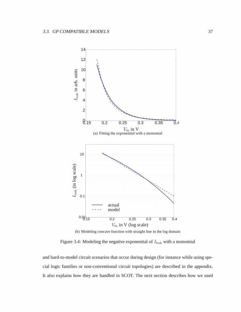
3.3. GP COMPATIBLE MODELS 37
0.15 0.2 0.25 0.3 0.35 0.40
2
4
6
8
10
12
14
Vth in V
I lea
kin
arb.
un
its
(a) Fitting the exponential with a monomial
0.15 0.2 0.25 0.3 0.35 0.40.01
0.1
1
10
Vth in V (log scale)
I lea
k(in
log
scal
e)
actualmodel
(b) Modeling concave function with straight line in the log domain
Figure 3.4: Modeling the negative exponential ofIleak with a monomial
and hard-to-model circuit scenarios that occur during design (for instance while using spe-
cial logic families or non-conventional circuit topologies) are described in the appendix.
It also explains how they are handled in SCOT. The next section describes how we used

38 CHAPTER 3. OPTIMIZATION FOR ENERGY-EFFICIENCY
SCOT on 32-bit adders to derive the overall E-D tradeoff of CMOS 32-bit addition.
3.4 Circuit case study: 32-bit adder
Adder structures are ubiquitous in modern digital systems and are often present in criti-
cal timing blocks. Consequently, designers have studied adder topologies extensively and
have developed many techniques to improve addition algorithms [96]. While initial papers
[62, 46, 55, 30] focused mainly on performance, recent research [100, 67, 54] has also
focused on energy, now a critical issue in digital design. Using SCOT, we extended this
work by systematically exploring 32-bit custom designed adder topologies for their energy-
efficiency [68]. We developed a relation between topological choices and energy-efficiency
by comparing the Pareto-optimal E-D tradeoff curves of selected adder topologies in dif-
ferent logic styles, based on sizing, supply voltage and threshold voltage optimization.
Many architectures in different logic styles have been proposed, so adders are a rich area
to explore. In addition, their layout is well known, so we canestimate the wire capacitance
in different topologies and logic styles with good confidence. To run this experiment, we
made schematics of several 32-bit adders with proper wire load estimates, and generated
their E-D tradeoff curves. The lower bound of all curves gives the overall E-D tradeoff
curve for 32-bit addition and indicates which topology and logic style is most energy-
efficient for each region of the E-D space. These curves are discussed in Section 3.4.3.
In order to distinguish different adder topologies for energy-efficiency, before dis-
cussing these results, the next section describes the topological parameters that affect en-
ergy and delay. Next we describe the design constraints thatwe include in the optimization.
The results and insights obtained using this tool are described in Section 3.4.3, where we
compare the Pareto-optimal E-D tradeoff curves of various adders for a common set of

3.4. CIRCUIT CASE STUDY: 32-BIT ADDER 39
design constraints.
3.4.1 Adder topologies
We focus on circuits that add twoN bit numbers to produce anN + 1 bit result. This
operation basically consists of “propagating” the carry “generated” at any of the bit po-
sitions to all the higher positions. The final carry at each bit is then XORed with the bit
sum to produce the sum at that bit position. Thus adder topologies can be separated into
their Sum Generation Logic (SGL) that produces the bit sums and their Carry Propagation
Logic (CPL) [94]. As CPL dominates the adder delay and energy, we use the following
four parameters of the CPL (based on Harris’s work [28]) to describe adder topologies.
1. Radix (R): In tree adders, we defineR as the average number of bits combined at
each logic stage3 of the CPL. In linear carry-skip or carry-select adders, R refers
to the average number of bits combined per stage to generate ablock Propagate-
Generate (PG) term.
2. Logic depth (L): L indicates the total number of stages in the CPL, and is at least
logRN for anN-bit adder. Note that the number of logic stages in the adder can be
more thanL.
3. Fanout (F ): F represents the maximum logical branching seen by any stage in the
CPL.
4. Wiring tracks (T ): T measures the maximum number of wires running across the bit
pitch between any successive levels of the CPL.
3To avoid confusion between a logic operation and the number of transistor stages needed to implementit, we consider every stage, including simple inversion, asa logic stage

40 CHAPTER 3. OPTIMIZATION FOR ENERGY-EFFICIENCY
2
1
0
3
45
2
1
0
4
3
2
1
0
3
4
2
1
0
3
4
2
1
0
4
3
5
2
1
0
3
4567
msb inputs
logi
cde
pth
a) Kogge Stone (2,4,8,2)
b) Knowles 4421 (2,2,4,5)
c) Sklansky 4421 (2,1,4,9)
d) Ladner Fischer 1 (2,1,5,5)
e) Brent Kung (2,1,7,2)
f) Han Carlson 1 (2,4,5,2)
Figure 3.5: CPL dot diagram of selected adders with their (R, T, L, F ). Solid lines andcircles are PG signals and PG combine cells, dashed lines anddiamonds are carry signalsand carry generate cells, and empty circles represent wiresor buffers.
For ease of visualization, CPL is usually represented usingdot diagrams, where the dots
mean logical operations on PG signals. The inputs are bit PG signals and the outputs are the
final carries to the different bit locations. Figure 3.5 shows the CPL dot diagrams of selected
16-bit radix 2 adder topologies with differentT , L andF numbers. For carry generation,
R, L, F , andT are inter-dependent [28]. Brent-Kung, Sklansky [80] and linear ripple-carry
adders have the least number of wire tracks (T = 1). Kogge-Stone and Sklansky adders are
examples of minimum logic depth adders [46]. Kogge-Stone and linear ripple-carry adders
haveF = 2, while a 32-bit Sklansky adder hasF = 17. For a given radix, Kogge-Stone
(KS), Brent-Kung (BK) and Sklansky4 maximize one of the three parametersT , L, and
4The Sklansky CPL design belongs to the Ladner-Fischer [49] family of adders. However Sklanky’sadder [80] predates Ladner-Fischer adders and can be easilyreduced to Ladner-Fischer design with removal

3.4. CIRCUIT CASE STUDY: 32-BIT ADDER 41
F respectively while minimizing other two. The Knowles, Ladner-Fischer (LF) and Han-
Carlson (HC) topologies [46] tradeoff two of these three parameters keeping the third fixed
[28]. Simple linear adders can also be described usingR, T , L andF . For example, the
32-stage ripple-carry adder can be said to have(R, T, L, F ) = (1, 1, 32, 2). A carry skip
and/or sum-select scheme in linear adders can be similarly described based on how they
modify the topology.
For complete analysis, we consider the following frequently occurring design scenarios.
1. External buffering: Inverters can be added at all the inputs or all the outputs of the
adder to best match the load it is driving, without changing its R, T , andL num-
bers, though with a possible inversion of the resulting sum.Hence for a given adder
topology and design constraints, we optimize with all possible external buffering and
choose the best of the tradeoff curves. This allows for a faircomparison between
adders with differentL.
2. Internal buffering and restructuring: Logic functions can be evaluated using a sin-
gle complex high fanin (higher valency) gate or a series of smaller low fanin (lower
valency) gates. The radixR is smaller in the latter case5. In our definition, R depends
on the number of stages needed to do a particular logic operation on a given number
of input bits. Thus, inverters appended to a complex gate in the middle of the crit-
ical path (as opposed to external buffering) reduces the overall radix. For example,
a domino gate that consumes four bits and generates a 4-bit PGterm has a radix of
2, because the dynamic gate and the inverter are two separatestages of computation.
of conditional-sum logic. Hence in this paper, we will use refer the Ladner-Fischer adder with highest F asSklansky design.
5In adder literature, radix typically refers to the logic operation and “valency” refers to its implementation.However, from circuits point of view a higher radix CPL implemented with lower valency gates behavessimilar in energy-delay to a lower radix CPL. Hence, for extracting the E-D tradeoff, we consider valencyand radix as equivalent and use radix in this research.

42 CHAPTER 3. OPTIMIZATION FOR ENERGY-EFFICIENCY
A radix 4 domino design would consist of alternating 4 input dynamic and 4 input
static stages. Even for the same radix, however, one can havetwo different designs.
For example, a 4 input gate followed by an inverter and a two level tree of 2 input
gates are both radix 2, but use different implementations. In these cases, we pick the
best of the two designs for comparison.
3. Sum selection:The SGL usually consists simply of XOR logic. However, in sum
select adders, the SGL generates a pair of speculative sums,to be correctly chosen
when the respective carry arrives. Sum selection is a very common technique used
for high performance adders today [62, 100]. Because only every kth carry needs to
be generated and fanned out tok muxes, ak-bit sum selection scheme re-distributes
the logical fanout of the CPL by increasing the fanout of the final carry tok. This can
potentially change theF of the CPL, independent of itsR,T andL, creating multiple
adders with the sameR,T andL numbers. Because the CPL is a more critical part of
the adder, we first find the most energy-efficient CPL structure and then explore the
related sum selection techniques. The CPL and SGL, being in parallel, are almost
independent for optimization purposes. This sequential procedure should therefore
give optimal results.
4. Ling adders [51]: These use a reformulation of the Propagate-Generate (PG) equa-
tions of tree adders. Because Ling’s equations are also associative and fall into a
tree structure, they can be described usingR, T , L andF . In this work, we look at
the best PG adder structures and then compare them with similarly constructed Ling
adders. Sum selection schemes are separately explored in both cases.

3.4. CIRCUIT CASE STUDY: 32-BIT ADDER 43
3.4.2 Design Constraints
In our analysis we focus on three principal design metrics: energy, delay, and output load
(Cout). We optimize adders for sizing, supply (Vdd) and threshold voltages (VthN andVthP).
For a given Cout, we generate E-D tradeoff by optimizing the delay at different total energy
constraints.
Most of the critical wires in an adder run across bits and thustheir lengths are set by the
bit pitch. Wires along the bit pitch generally have lengths set by the number of transistors in
that bit pitch, hence we capture these using fixed capacitances. This assumption is invalid in
cases of high energy, when gate sizes become very large. However, in this region, transistor
capacitances dominate the wire capacitances anyways, so the resulting sizing errors should
be small.
We constrained the input capacitance (Cin) at any input to beless than 25fF, or roughly
15µm of transistor width. This is a reasonable load within the driving capability of library
flip-flops in a 90nm CMOS technology. Except at the high energypoints, this constraint
does not come into play.
For small loads, if the Cin constraint is active, the adder has already entered the region
of diminishing performance returns for added energy. For large loads, external buffering at
the output of the adder is always more efficient than increasing the sizes of the gates in the
adder. Adding inverters at the output generally reduces therequired input capacitance to
fall within the specified Cin constraint. To check the effectof a Cin constraint we optimize a
few adders without the input constraint and show that it makes little difference. Reasonable
signal slopes are maintained at every net, by limiting the delay of every logic stage. The
minimum transistor width is constrained to0.25µm. Vdd ranges from 0.5V to 1.3V, while
Vths range continuously from about 0.2V to 0.4V. Both are commonfor all gates in the
netlist. All dynamic gates have footers, keepers and intermediate precharge transistors,

44 CHAPTER 3. OPTIMIZATION FOR ENERGY-EFFICIENCY
which are used for stacks of three or more transistors. The sizes of all these peripheral
devices are ratioed to their respective NMOS pull-down transistors in order to track their
sizes under optimization. The final XOR gate for sum generation (or sum select mux) is
static in all cases except for dual-rail domino circuits.
The activity factor of nets can differ by orders of magnitudeespecially in domino
adders. This means the gates on low activity nets can potentially be sized larger and still
not dissipate too much dynamic energy. The sizes however, donot blow up because they
are still constrained by the Cin.
Because different topologies have different logic depth, fanout, and internal loading and
hence can be optimal under different load conditions, we generate the pareto-optimal E-D
tradeoff curves for different values of Cout.
3.4.3 Results and analysis
The delay of anN-bit adder primarily depends on how fast the carry reaches each bit
position. Parallel prefix logic networks [46], which use tree structures to compute the
carry, are very efficient for largeN [87]. Hence, for a systematic traversal of adders, we
start with the three corner radix 2 parallel prefix adders based onL, T andF (Section 3.4.1)
built in static CMOS logic. We will show later in this sectionthat 2 is the optimal radix.
We first consider the corner adders – Kogge-Stone, Brent-Kung and Sklansky – de-
signed in 90nm static CMOS logic. We specify the delay in FO46, which is 31ps7 for our
technology. Figure 3.6 shows the pareto-optimal E-D tradeoffs of these adders for Cout =
25fF and Cout = 100fF. The adder designs include external buffering if necessary. Figure
3.6(b) also shows the E-D curve for a Sklansky adder with no input capacitance constraint.
6An FO4 delay is the delay of single inverter driving 4 copies of itself from a step input. The FO4 delayis typically used to characterize the technology speed.
7While the FO4 delay changes withVdd andVth, the unit used here is measured at nominalVdd andVth.
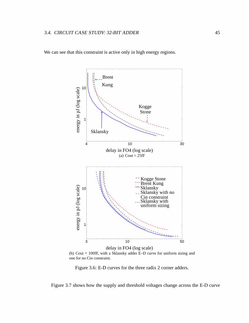
3.4. CIRCUIT CASE STUDY: 32-BIT ADDER 45
We can see that this constraint is active only in high energy regions.
4 10 30
1
10
delay in FO4 (log scale)
ener
gy
inp
J(lo
gsc
ale)
Brent
Kung
KoggeStone
Sklansky
(a) Cout = 25fF
3 10 50
1
10
delay in FO4 (log scale)
ener
gy
inp
J(lo
gsc
ale) Brent KungKogge Stone
SklanskySklansky with noCin constraintSklansky withuniform sizing
(b) Cout = 100fF, with a Sklansky adder E–D curve for uniform sizing andone for no Cin constraint.
Figure 3.6: E-D curves for the three radix 2 corner adders.
Figure 3.7 shows how the supply and threshold voltages change across the E-D curve

46 CHAPTER 3. OPTIMIZATION FOR ENERGY-EFFICIENCY
for a Sklanksy adder. WhenVdd reaches its upper bound, the threshold voltages continue
to decrease. At the lower bound ofVdd, the design becomes infeasible due to signal slope
constraints, even thoughVths have not hit their upper bounds. If the input activity factor is
increased (decreased), the supply and threshold voltages both decrease (increase), increas-
ing (decreasing) the leakage power in relation to the increase (decrease) in active power.
4 10 400
0.5
1
1.5
4 10 400.15
0.2
0.25
0.3
delay in FO4 (log scale)
volta
ge
inV
volta
ge
inV
VddVthP
VthN
Figure 3.7: Change inVdd andVths across the E–D space for a Sklansky adder.
The E-D curves show diminishing returns as we go towards either higher performance
or lower energy. At higher energies, as device sizes continually increase, the effect of
wires and Cout decreases. After a certain point, the gates would largely be driving their
own parasitic capacitance and further improvement in delaywould not be possible. With
Cin constrained, after a certain energy, the design becomesidentical to one based solely
on logical effort [87], for which the marginal cost of energyfor improvement in delay is
infinite. Similarly, as energy is lowered, the supply and threshold voltage both change
(see Figure 3.7) until the design enters a region where, analogous to the minimum delay
solution, the marginal cost in delay for lowering the energyis very high.

3.4. CIRCUIT CASE STUDY: 32-BIT ADDER 47
The three radix 2 adders in Figure 3.6 each minimize two parameters out ofL, T and
F , at the cost of the third. Our experiments indicate that the Sklansky adder, which has
the highestF , but smallestL and T , is the most energy efficient. Clearly, these three
parameters do not trade equally with each other.
A large logical fanout at a particular stage does not necessarily imply that that stage
will be slow. What matters to the delay is theelectrical fanout (due to capacitive loading).
In a Sklansky adder, at everynth stage of the CPL tree, the carry drives2n + 1 gates. After
optimal sizing, we find that of these2n +1 PG combine gates at the(n+1)th stage, the one
gate that drives2n+1 + 1 PG combine cells at the next stage (or the largest load in general)
is sized much larger than the others, resulting in an overallelectrical fanout closer to 2.
This optimization of electrical-vs-logical fanout arisesdue to the possibility of differential
sizing of the gates at the same stage. With its highestF of 17, Sklansky adder can take
maximum advantage of differential sizing.
Unlike F , L has a real cost. A Brent-Kung adder has the sameT , but almost twice the
L as the Sklansky adder. This may seem useful for driving a large Cout, but inverters are
far more efficient than P/G gates and can always be padded to a lower logic depth design
to make up for the required gain at lower energy cost.
Like L, T also has real costs. A largerT means a higher portion of the total energy
consumed in wires. With its smallestT of 1, the Sklansky design spends most of the
energy budget in driving useful logic, with the least amountwasted in wires. A Kogge-
Stone adder, having the largestT , suffers from high energy loss to result in poor energy
efficiency. Figure 3.8 shows the percentage of total adder energy8 consumed in wires for
the three adders. Note that wire energy changes withVdd, which changes with the optimal
E-D point.
8This excludes the energy consumed in output loads (Cout).

48 CHAPTER 3. OPTIMIZATION FOR ENERGY-EFFICIENCY
0 10 20 30 400
5
10
15
20
25
SklanskyKogge StoneBrent Kung
delay in FO4
%o
fto
tale
ner
gy
Figure 3.8: Energy consumed in wires.
At lower energies, resources are constrained and adders with fewer gates have an ad-
vantage. The Brent Kung adder is most economical in gate count. Hence it comes closer to
Sklansky at lower energies, unlike Kogge-Stone, which has acomparable number of gates
to Sklansky, but more wires.
To confirm our inferences about the Sklansky design we optimized its two closest radix
2 adders – a LF adder with an extra logic level ((R, T, L) = (2, 1, 6)) and a Knowles
adder with an extra wire track ((R, T, L) = (2, 2, 5)). We also optimized a 2-bit sum select
Sklansky adder to check if reduced fanout (F = 8) in Sklansky CPL at the cost of increased
fanout for the final carry gives any benefit. We found that the cost of generating the condi-
tional sum in SGL was more than the advantage of having CPL andSGL in parallel. The
results shown in Figure 3.9 confirm that Sklansky was better than its three closest relatives.
Due to lower gate count, the selected Ladner-Fischer adder tends to compete with Sklansky
adder at lower energies.

3.4. CIRCUIT CASE STUDY: 32-BIT ADDER 49
4 10 40
1
10
Sklansky
delay in FO4 (log scale)
ener
gy
inp
J(lo
gsc
ale)
Sklansky 2bit sum selectKnowles 84421Ladner Fischer 1
Figure 3.9: Comparison of Sklansky adder E–D curves to its closest neighbors and to a2-bit sum select scheme.
Other logic styles and topologies
Given that the effect of loading and parasitics is similar inall logic styles, the topology that
is the most energy-efficient in one, will be the most energy-efficient in the other as well.
Following are the results of our experiments on other logic styles designed on the basis of
the results from static CMOS logic.
1. Domino and dual rail designs: We made Sklansky designs in radix 2 domino and
dual rail domino logic9. Similar to the static case, a fully dynamic 2-bit sum select
scheme does not give any benefit. However, a 2-bit sum select using static SGL im-
proves the energy-efficiency due to lower activity factor inthe SGL. On the other
hand, dual-rail designs consume almost twice the energy compared to domino de-
signs with the only benefit that the XORs in the SGL are faster.Hence they are better
9Because the fanin of the domino gate (dynamic gate and inverter) is 4, some researchers [100] call thisradix 4.

50 CHAPTER 3. OPTIMIZATION FOR ENERGY-EFFICIENCY
than the domino designs only at high energy by a small amount.Figure 3.10 shows
the E-D curves of selected Sklansky domino/dual-rail topologies.
3 10 30
1
10
delay in FO4 (log scale)
ener
gy
inp
J(lo
gsc
ale)
domino Ling
domino PG with max 5 transistor stack
domino PG 2b sum sel withstatic SGL & max 4 tran. stack
domino PG with max 4 tran. stack
domino Ling 2b sumsel. with static SGL
dual rail Ling
Figure 3.10: Comparison of Sklansky domino and dual-rail domino tree adders.
Ling adder performs about 5% better in delay than the PG adderif only 4 transistor
stacks are allowed, but it is worse than an equivalent PG adder (which will have a 5
transistor stack in the first dynamic gate). However, as mentioned before in Section
2.1.4, our modeling of the parasitic delay is most optimistic in the 5 stack gate, so
we expect the two designs to be comparable in practice. Due tolarge fanin right at
the inputs, the Cin constraint becomes active in these adders pretty early on, which
is why the 4 stack PG adder looks better at higher energy.
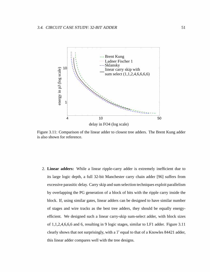
3.4. CIRCUIT CASE STUDY: 32-BIT ADDER 51
4 10 50
1
10
Brent KungLadner Fischer 1Sklanskylinear carry skip withsum select (1,1,2,4,6,6,6,6)
delay in FO4 (log scale)
ener
gy
inp
J(lo
gsc
ale)
Figure 3.11: Comparison of the linear adder to closest tree adders. The Brent Kung adderis also shown for reference.
2. Linear adders: While a linear ripple-carry adder is extremely inefficient due to
its large logic depth, a full 32-bit Manchester carry chain adder [96] suffers from
excessive parasitic delay. Carry skip and sum selection techniques exploit parallelism
by overlapping the PG generation of a block of bits with the ripple carry inside the
block. If, using similar gates, linear adders can be designed to have similar number
of stages and wire tracks as the best tree adders, they shouldbe equally energy-
efficient. We designed such a linear carry-skip sum-select adder, with block sizes
of 1,1,2,4,6,6,6 and 6, resulting in 9 logic stages, similarto LF1 adder. Figure 3.11
clearly shows that not surprisingly, with aT equal to that of a Knowles 84421 adder,
this linear adder compares well with the tree designs.

52 CHAPTER 3. OPTIMIZATION FOR ENERGY-EFFICIENCY
While their L is comparable forN = 32 bits, the logic depth of linear adders in-
creases faster than that of a tree structure, where it is logarithmic with N . For exam-
ple, forN = 64, L for Sklansky adder increases by unity, whereas for the best linear
adder, it increases by 3. Hence linear adders are less efficient for higherN .
Optimal radix
From our definition of the radix, a logical operation performed onN inputs inp stages has
a radix oflogpN regardless of the kind of gates used. For delay,p is optimal (popt) when
each stage has a delay of about a FO4 [87]. The value ofpopt depends on the load and the
kind of gates used in the design. A gate doing more logic than simple inversion requires
more effort and hence is inherently slower. Thus gates in higher radix adders are inherently
slower. Accounting for this logical effort, calculation shows that for all reasonable adder
loads (where Cout is at least about Cin), the number of stagesin a minimum logic depth
radix 2 adder is about equal to or less than their respectivepopt. The logic depth of higher
radix adders may fall short ofpopt but that can be made up by external buffering. Even for
bigger adders (i.e.N ≥ 32), popts for R ≥ 2 are about the same [29] and big enough to
accommodate the logic depth of all adders withR ≥ 2.
Although for minimum delay, the delay per stage should be equal, the inherent slowness
of the higher fanin gates (in higher radix adders) coupled with higher logical fanout per
stage restricts the delay per stage to be always higher than acertain amount10. Also, because
parasitic delay grows at least as the square of the number of inputs [96], the parasitic delay
of higher fanin gates dominates any gain from the reducedL, given that inverters need
to be padded to reachpopt stages. Complex high fanin gates like the ones that produce the
group generate signals grow in the number of parallel transistor stacks as well, significantly
10for reasonable output load (Cout) on the adder.

3.4. CIRCUIT CASE STUDY: 32-BIT ADDER 53
increasing their parasitic delay. Therefore a radix of 2 is optimal for delay.
From the energy point of view, using higher fanin gates does not save on switching
activity. Adders being multiple output structures, the intermediate signals generated by
using trees of lower fanin gates are typically used for othercomputation. Also, while
the propagate function benefits from having a large fanin gate, as it is an AND function
and activity factor reduces with more inputs, switching simulations show that the generate
operation maintains the switching factor. Hence overall, higher fanin PG cells have only a
marginal reduction of switching activity over trees of lower fanin cells. For domino designs
however, because NMOS is faster than PMOS, it is better to have series NMOS stacks in
the dynamic gate than having PMOS stacks in the following static stage. Hence the gates
with four input dynamic gates followed by an inverter are more efficient than gates with
two input dynamic stage followed by a two input static stage.Note that the radix is 2 in
both cases.
To validate our intuition, we designed static CMOS 32-bit Sklansky adder, one with
radix 3 and another with radix√
6 (using alternate 3 bit and 2 bit combine stages). To
avoid the irregularity of a 32-bit radix 3 adder, we also designed 27-bit adders with radix 2
and 3. Figure 3.12 compares the E-D tradeoff and confirms our understanding. The results
remain unchanged for Cout = 25f.
Effect of buffers on energy-efficiency
External buffers increases the number of stages in the adder. Hence one might expect that
while they are useful for adders with small logic depth driving large loads, they would be
inefficient for an adder withL that is already at or bigger than the optimalL. However,
inverters are the most efficient drivers. Hence, in additionto buffering, padding inverters
at the output leads to a reduction in the size of the complex gates that precede them, thus

54 CHAPTER 3. OPTIMIZATION FOR ENERGY-EFFICIENCY
4 10 40
1
10
delay in FO4 (log scale)
ener
gy
inp
J(lo
gsc
ale)
27bitradix 2
27bit radix 3
32bit radix√
6
32bit radix 2
32bit radix 3
Figure 3.12: E–D tradeoff curves of 32-bit and 27-bit Sklansky adders of different radices.
saving energy. The reduction of gate sizes on the side paths helps to reduce the load on
the critical path and more than compensates for the increased delay due to the extra logic
stage. Figure 3.13 shows that while buffering is inefficientin the high energy region due
to the delay added by the extra inverter stage(s), as the energy budget is reduced, the same
design padded with a single inverter stage does much better than the original. The potential
increase in delay by adding an extra logic stage is more than compensated by the energy
benefit from smaller SGL gates, even in the Brent Kung adder, which already has a large
L. In fact, all the E-D curves shown in this paper are with a single inverter padding, except
for the dual rail ling adder design, which was more efficient without external buffering.
This is expected, because there the outputs are already driven by the inverter of the dual
rail domino gate. Selective padding of different paths can possibly bring more gains, but
would affect the logical functionality of the design.

3.4. CIRCUIT CASE STUDY: 32-BIT ADDER 55
4 5 64
10
5 64
10
delay in FO4delay in FO4en
erg
yin
pJ
(log
scal
e)
ener
gy
inp
J(lo
gsc
ale)
no bufferingno buffering
1 inv.1 inv.2 inv.2 inv.
Figure 3.13: Effect of external buffering on radix 2 Sklansky (left) and Brent Kung (right)adders.
3.4.4 Adder design space
The E-D tradeoff curves of the different adders across different logic styles intersect at
points where one adder achieves better energy efficiency than the other. Static adders are
good at low performance regions because, with lower switching activity factor and no clock
load, they consume lower energy; but they saturate quickly as higher performance is de-
sired, due to inherently slower gates (large logical effort). With lower logical effort gates,
dynamic adders have potentially higher performance and at higher energy they perform
much better than their static counter parts. The overall Pareto-optimal curve is the lower
bounding curve of all these curves. It gives an indication ofthe E-D space of optimally
designed adders. Figure 3.14 shows the complete 32-bit adder E-D space. Incidently, at or
before the point where Cin constraint becomes active, the next logic family takes over the
pareto-optimal curve. We can also observe that sensitivityof energy-efficiency toR,T , and
L depends on the location on E-D curve. At low energy side, wiretracksT have a large

56 CHAPTER 3. OPTIMIZATION FOR ENERGY-EFFICIENCY
3 10 40
1
10
delay in FO4 (log scale)
ener
gy
inp
J(lo
gsc
ale)
Sklansky static CMOS
Slkansky dom. Ling 2b sum sel.Sklansky dual rail Ling
Figure 3.14: 32-bit adder E-D space.Cload = 100fF
weight because they consume a greater portion of the energy budget. At low delay points
logic depth L matters more because every added stage adds a minimum delay, which causes
external buffering to be inefficient at high energies and enables the Kogge-Stone E-D curve
to cross the Brent-Kung one.
3.5 Summary
The goal of a circuit sizer is to optimally allocate the givenarea/energy among the different
devices in the netlist for maximum possible performance. The delay and energy of a gate
can be accurately modeled as posynomials. While the total energy is just a sum of many
posynomial terms, the overall delay can be easily obtained using sum andmax operations
on gate delays, with static signal timing propagation in thecircuit netlist. Using these

3.5. SUMMARY 57
elements, the deterministic circuit optimization problemcan be cast as a Geometric Pro-
gram, which can be solved efficiently. Although some important circuit issues like slope
constraints and transmission gate timing constraints are either difficult to model and/or in-
herently non-convex, suitable work-around can be obtainedin a convex framework, to drive
the optimizer to do correct sizing.
We developed this optimization framework in a tool called SCOT. SCOT helped us to
efficiently obtain the tradeoff curves for different 32-bitadder topologies. This information
not only helped us to gain valuable insights regarding the factors that make circuits energy-
efficient, but also gave us an overall picture of the energy-delay design space of 32-bit
adders.
The optimization shown in this chapter did not include variations as one of the param-
eters. In the next chapter, we will show how variations can significantly reduce the yield
of optimized designs and then describe the solutions we havecome up with to tackle the
statistical design problem.

58 CHAPTER 3. OPTIMIZATION FOR ENERGY-EFFICIENCY
Chapter 4
Optimization for robustness
In Chapter 2, we described the different process variationsthat can occur during fabrica-
tion. Variations cause the delay and energy of the fabricated designs to have a distribution
around the original specifications. Thus variations cause the fabricated chips designed for
one design point to scatter over a region in the energy-delayspace as shown in Figure
4.1(a). Some of these designs still lie on the Pareto-optimal curve and are therefore energy-
efficient. These can be binned for selling them with different energy-delay specs. It is very
unlikely that variations may result in a design that beats the Pareto-optimal curve, as it is
extremely unlikely that all the parameters in the chip are improved in the right direction.
Most of the scattered designs are on the upper-right of the Pareto-optimal curve, and there-
fore not energy-efficient. The parametric yield1 of a design is defined as the percentage of
functional fabricated designs that meet or exceed the specs. If we desire a certain yield in
the scenario in Figure 4.1(a), the specification of the product will have to be relaxed. This
gives us a new energy-delay tradeoff curve for the fabricated designs that meet the new
specs. This curve can be greatly inferior to the curve we designed for. We really want to
1as opposed to functional yield which is the percentage of designs that have no functional defects. Unlessthere is ambiguity, henceforth in this thesis, we will referto parametric yield simply as yield
59

60 CHAPTER 4. OPTIMIZATION FOR ROBUSTNESS
optimize the efficiency of the circuits that are actually produced (i.e the yield curve). In-
cluding the process variation information in the circuit design process can lead to design of
robust circuits that would tolerate variations better. Such a design methodology where vari-
ation information is incorporated in the design phase itself is called “statistical design”, as
opposed to the traditional “deterministic design” where all device parameters are assumed
to be fixed to some average value or are assumed to be completely correlated with each
other. The design resulting from the use of only the nominal or average parameter values is
referred to as “nominal design”, while the design resultingfrom statistical design method-
ology will be termed as “robust design”. As shown in Figure 4.1(b), a robust design has a
tighter distribution and hence suffers a smaller degradation of the original Pareto-optimal
curve.
(a) Q95 E–D curve of nominal design (b) Improved E–D curve for robust design
Figure 4.1: Possible improvement inQ95 E–D curve with design for robustness
Under variations, the delay and energy of a circuit become random variables with a
Probability Density Function (PDF) which depends on the PDFof the individual gate de-
lays and energies. The robust Pareto-optimal tradeoff curve for a particular yield, say,α
can be obtained by optimizing such thatα percentile of the implementations have specs
that are better than the one we designed for. In this chapter we will attempt to solve this

4.1. ESTIMATING PERFORMANCE BOUNDS 61
statistical design problem.
The techniques to statistically handle delay and energy aredifferent due to the way
delay and energy relate to the design variables. We shall first focus on delay variations
and then focus on energy. In order to understand how individual gate delay variations
contribute to the overall delay distribution, we describe different methods of estimating the
circuit timing under gate delay uncertainty [45]. These analysis techniques will be useful
as a guide to statistical design. Using statistical analysis, we show how local independent
process variations adversely affect the delay of deterministically optimized designs from
the previous chapter. It is feasible to solve the statistical design problem exactly in some
special simple circuits. We discuss the formulation of the exact solution of statistical design
problem. The exact solution is extremely tedious to apply totypical circuits. To overcome
this problem we have derived some effective heuristics based on insights from the exact
solution and statistical analysis, which we shall describenext.
4.1 Estimating performance bounds
Consider the overall circuit delayTd, given by
Td = max{d(p) | p ∈ P},
whereP denotes the set of all paths andd(p) represents the delay of pathp. We will
consider energy estimates in Section 4.6. The PDF ofTd depends on the extent and nature
of process variations. Several scalar performance measures can be used to characterize the
delay metric of the circuit. Examples include:
• Expected value:µ(Td).

62 CHAPTER 4. OPTIMIZATION FOR ROBUSTNESS
• Probability of missing a targetT0: prob(Td ≥ T0).
• Expected tardiness:µ(max{Td − T0, 0}).
• α-percentile ofTd: Qα(Td) = inf{t : prob(Td ≤ t) ≥ α},
whereinf{} is the infimum2 of a set of numbers.
Exact Statistical Static Timing Analysis (SSTA) which extends the traditional Static
Timing Analysis (STA) by propagating PDFs instead of numbers is very difficult, except in
a few special cases. The problem is that the evaluation of gate delay as given in Equation
3.1 involves both, addition and maximum of random variables. While there are common
families of distributions that are closed under addition, and others that are closed under
maximum (or minimum), no practical family of distributionsfor gate delay is closed under
both.
We can, however, say many things about the distribution ofTd. For example, if gate
delayD is Gaussian, then delay of each path through the netlist is a Gaussian andTd
is the maximum of a number of correlated Gaussian random variables. There are many
bounds and asymptotics known for such distributions [78]. Ageneral and common ap-
proach is based on approximating or bounding the distributions of the gate output timings,
by recursively bounding (or approximating) the delay distribution of gatei in combination
with bounds (or approximations) of the distributions of thesignal arrival times at its input
[20, 22, 26, 52, 58, 74, 79, 95]. LetTnom represent the delay of the nominal design where
the gate delays are assumed to be fixed to their mean values. When the distribution ofD is
very tight, i.e., D is very close to its meanµ(D) with high probability, we expectTnom to
give a good approximation ofTd.
2The infimum of a subset of some set is the greatest element, notnecessarily in the subset, that is less thanor equal to all other elements of the subset.

4.1. ESTIMATING PERFORMANCE BOUNDS 63
In fact,Tnom is always an underestimator ofTd, in the following sense.
Tnom = T (µ(D)) ≤ µ(Td) = µ(T (D)), (4.1)
whereT () represents the overall circuit delay as a function of gate delays. This holds
for any distribution onD. One interpretation of this inequality is that by adding zero-
mean statistical variation to any gate delay, we can only increase the expected value of the
overall delay. This inequality is a direct application of Jensen’s inequality [10], along with
the observation thatT () is a convex function of the gate delays. Convexity follows since
T () is the maximum of a set of sums – a linear function – of gate delays [10].
Equality holds in (4.1) if and only if there is a unique path that is always critical [32].
The criticality of a path is defined as the fraction of manufactured instances it has the high-
est delay. Similarly the criticality of a gate can be defined as the fraction of manufactured
circuits in which it appears on a critical path. If there are relatively few paths with high
criticality, the difference between the left and righthandsides of (4.1) can be relatively
small. In other cases,e.g.when all gates uniformly have low criticality, the difference can
be relatively large as we shall see in Section 4.2.
4.1.1 Performance bounds via stochastic dominance
Let FU(t) = prob(U ≤ t) denote the Cumulative Distribution Function (CDF) of the
scalar random variableU. A scalar random variableX is said to bestochastically less than
or equal toanother scalar random variableY (denoted byX ≤st Y) if FX(t) ≥ FY(t)
holds for all t. Stochastic inequality can also be expressed in terms of percentiles. Let
Qα(U) = inf{t : prob(U ≤ t) ≥ α} denote theα-percentile ofU. Then,X ≤st Y if and
only if Qα(X) ≤ Qα(Y), for all α ∈ (0, 1). All of the performance measures described

64 CHAPTER 4. OPTIMIZATION FOR ROBUSTNESS
in the beginning of Section 4.1 are monotone with respect to stochastic dominance. For
example, ifX ≤st Y, the expected tardiness ofX is no more than the expected tardiness
of Y.
A basic result is that for any random variablesX1, . . . ,Xp, no matter what their joint
distribution is, their maximum is always stochastically greater than or equal to each of
them:
Xi ≤st max{X1, . . . ,Xp}, i = 1, . . . , p.
SinceTd is the maximum of all path delays, it is always stochastically greater than or
equal to the delay of any path, no matter what the duration distributions are, and whether or
not they are independent. We conclude that for each of the performance measures described
in Section 4.1, the maximum of the performance measure over all paths is a lower bound
on the performance measure ofTd. For example, theα-percentile ofTd satisfies
maxp∈P
Qα(Dp) ≤ Qα(Td), (4.2)
whereP is the set of all paths, andDp is the delay of pathp. This gives us a method
for obtaining a lower bound on a performance measure when thedurations are Gaussian.
In this case, each path delay is Gaussian, and its performance measure can be calculated
exactly as a function of its mean and variance. By taking the maximum of these measures
over all of the paths (or a subset) we obtain a lower bound on the performance measure for
Td. (Unfortunately, there is no simple recursion, like in static timing analysis to calculate
Tnom, for calculating the maximum of theα-percentile over all paths.)
For future use, we give a very simple lower bound on percentiles ofTd. By Jensen’s
inequality,Tnom is a lower bound onµ(Td). Since gate delays are non-negative and have
close to Gaussian or otherwise well behaved distributions,we can argue that for every path,

4.1. ESTIMATING PERFORMANCE BOUNDS 65
its expected delay is less than or equal to itsα-percentile for values ofα of interest, such
asα = 0.95.
µ(Di1 + · · ·+ Dik) ≤ Qα(Di1 + · · · + Dik), ∀ p = (i1, . . . , ik) ∈ P. (4.3)
With this assumption,Tnom is a lower bound on theα-percentile ofTd:
T (µD) = maxp=(i1,...,ik)∈P
{µ(Di1) + · · ·+ µ(Dik)} ≤ Qα(Td). (4.4)
4.1.2 Performance bounds via surrogate netlists
A hypothetical netlist where the delay of every gatei, di is fixed and given bydi = µ(Di)+
κiσ(Di), whereσ(U) denotes the standard deviation of a scalar random variableU, is
called a surrogate netlist of the original netlist. We callκi ≥ 0 the margin coefficients.
Note that the original netlist is the surrogate netlist withall margin coefficients zero. We
can derive some bounds on the percentiles (or other measures) of Td from the STA of its
surrogate netlist for proper choice of margin coefficients.
We consider the case in which the gate delay distributions are independent and Gaus-
sian. The delay of pathp = (i1, . . . , ik) is also Gaussian, and itsα-percentile can be
expressed as
Qα(Dp) = µ(Di1) + · · ·+ µ(Dik) + Φ−1(α)(σ(Di1)
2 + · · ·+ σ(Dik)2)0.5
where
Φ(α) =1√2π
∫ α
−∞e−t2/2 dt (4.5)
is the CDF of a unit Gaussian variable.

66 CHAPTER 4. OPTIMIZATION FOR ROBUSTNESS
We will now relateQα(Dp) to the delay of a path in a surrogate netlist, using the
Cauchy-Schwartz inequality
(u21 + · · ·+ u2
k)0.5 ≥ a1u1 + · · · + akuk, (4.6)
provideda21 + · · · + a2
k ≤ 1. This gives
Qα(Dp) ≥ µ(Di1) + · · ·+ µ(Dik) + Φ−1(α)(a1σ(Di1) + · · · + akσ(Dik)),
provideda21+· · ·+a2
k ≤ 1. Note that the righthand side here is the delay of the pathp, in the
surrogate netlist withκi = Φ−1(α)ai. This operation essentially allows us to break open
the root mean square (RMS) calculation of the standard deviation of a path and convert it
into additive terms.
We can make several simple choices of theai so that the requirementa21 + · · ·+ a2
k ≤ 1
holds for every path. One simple choice is
ai = l−1/2max ,
wherelmax is the maximum length of any path in the netlist. Another choice is
ai = l−1/2i ,
where
li = max{l(p) | pathp contains gatei}
is the length of the longest path that contains gatei.
The quantitylmax is readily computed using recursion as used in STA wherelmax =

4.1. ESTIMATING PERFORMANCE BOUNDS 67
Tnom with all gate delays equal unity. A variation on this recursion can be used to efficiently
calculate the quantitiesli. We use a STA recursion to compute the length of the longest path
from inputs to gatei, and another recursion, starting at the outputs and workingbackward,
to find the length of the longest path from each gatei to any output. We add these two
quantities at each node to obtainli.
The bounds above, along with (4.2), imply that the delay of the surrogate netlistTnom,
with the choice of margin coefficients
κi = Φ−1(α)lmax−1/2, (4.7)
or the more sophisticated choice
κi = Φ−1(α)l−1/2i , (4.8)
is a lower bound onα-percentile ofTd. Note that the timing of a surrogate netlist can be
computed efficiently using STA.
The same lower bound on theQα(Td) holds with correlated Gaussian duration distri-
butions, provided that the covariance of any two gate delaysis nonnegative. When this is
the case, the standard deviation of the delay of any path is less than or equal to the standard
deviation when the gate delays have the same standard deviations, but are uncorrelated.
It is also possible to obtainupper boundson a performance measure, such as theα-
percentile ofTd, that have a similar form. As an example, we consider the casewhere the
gate delays are Gaussian and can be correlated. Let|P| be the total number of paths from
sources to sinks andY1, . . . ,Y|P| denote the delays of all such paths,i.e.,
Td = max{Y1, . . . ,Y|P |}.
68 CHAPTER 4. OPTIMIZATION FOR ROBUSTNESS
Let Z1, . . . ,Z|P| denoteindependentrandom variables whose distributions are identical to
those ofY1, . . . ,Y|P|, respectively, that is,
Td = max{Z1, . . . ,Z|P|}.
A basic result on stochastic comparison between random variables shows that
Td ≤st Td.
It follows that theα-percentile ofTd is less than or equal to that ofTd
Qα(Td) ≤ Qα(Td).
Now the idea is to computeQα(Td), which is relatively easy. SinceZi are independent of
each other, the righthand side can be expressed as
Qα(Td) = inf{t |
|P|∏
i=1
FZi(t) ≥ α
}. (4.9)
We do not know whatinf{t} is, but we are looking for an upper bound. So let us chooset
that is high enough to satisfy Eq. 4.9 as
t = maxi=1,...,|P|
(µ(Zi) + Φ−1(α1/|P|)σi(Zi)).
SinceZi are Gaussian, we haveFZi(t) ≥ α1/|P|, and hence
∏|P|i=1 FZi
(t) ≥ α. This along
with (4.9) leads to the inequality
Qα(Td) ≤ maxi=1,...,|P|
(µ(Zi) + Φ−1(α1/|P|)σi(Zi)).

4.1. ESTIMATING PERFORMANCE BOUNDS 69
We now show how to relate the righthand side of the inequalityabove to the delay of a
path in a surrogate netlist. LetZi be the delay of a path consisting of gatesi1, . . . , ik:
Zi = Dii + · · ·Dik .
Since(x21 + · · ·x2
k)0.5 ≤ x1 + · · ·+ xk for xi ≥ 0, we have
µ(Zi) + Φ−1(α1/|P|)σi(Zi) =k∑
j=1
µDij + Φ−1(α1/|P|)( k∑
j=1
σij (Dij)2)0.5
≤k∑
j=1
(µ(Dij) + Φ−1(α1/|P|)σij (Dij)
).
The righthand side is the delay of the pathp = (i1, . . . , ik) in the netlist with gate delays
µ(Di) + Φ−1(α1/|P|)σi(Di). Now, we have the bound
Qα(Td) ≤ γ,
whereγ is the delay of the surrogate netlist with gate delaysµ(Di) + κσi(Di), where
κ = Φ−1(α1/|P|).
The values ofκ required to obtain the upper bound taper off roughly as the log of the
number of paths as shown in Figure 4.2. For example, for a netlist where the number of
all paths is3000, the choice ofκ = 4.14 gives an upper bound for its0.95-percentile. Of
course, the upper bound thus obtained on theα-percentile is tighter if paths in a netlist are
mostly independent.
To summarize, we have described some computationally efficient and relatively simple
performance bounds. These bounds require only the means andvariances of the gate delay,

70 CHAPTER 4. OPTIMIZATION FOR ROBUSTNESS
100
101
102
103
104
105
1061
2
3
4
5
6
κ
# of paths
α = 0.9α = 0.95α = 0.99
Figure 4.2:κ required for estimating the upper bound ofQα(Td)
and may not be as accurate as others that have been proposed,e.g., the one given in [4],
which rely on the same information. But the main purpose of the bounds given in this sec-
tion is not statisticalanalysiswhich can be done efficiently and accurately by Monte Carlo
analysis. The bounds given in this section can be used to provide bounds on suboptimality
of a statisticaldesignand develop heuristics for robust sizing. We describe this in Sec-
tion 4.4. In Section 4.1.4, we shall see how these bounds perform on some representative
circuits.
4.1.3 Monte Carlo analysis
While exact analysis of the distribution ofTd is very difficult, Monte Carlo methods can
be used to approximately compute the distribution, along with the performance measures
or other quantities of interest. In this section we describebasic Monte Carlo analysis of a
netlist; more sophisticated methods can be used to get higher accuracy with fewer samples,
4.1. ESTIMATING PERFORMANCE BOUNDS 71
or combine Monte Carlo simulation with bounding methods [13, 81, 86].
In basic Monte Carlo analysis, we drawM independent samplesd(1), . . . , d(M) from the
distribution of the random duration vectorD, and createM distinct netlist instantiations.
For each instance, we can efficiently evaluate its delay using STA, to obtainT (1)nom, . . . , T (M)
nom .
The sampled delaysT (1)nom, . . . , T (M)
nom , are, of course, independent samples from the distri-
bution ofTd.
Percentile estimation
To estimateQα(Td) from the samplesT (1)nom, . . . , T (M)
nom , we first re-order them so that
T (1)nom ≤ · · · ≤ T (M)
nom .
Once re-ordered,T (k)nom is called thekth order statisticof Td. A simple estimateQα(Td) of
the percentile is given by
Qα(Td) = T (⌈Mα+1⌉)nom
where⌈x⌉ denotes the integral part ofx ∈ R. This estimate is asymptotically consistent
and its variance is inversely proportional toM under the mild assumption that the PDF of
Td, fTd(Qα(Td)), is always positive [93].
Criticality index estimation
Under mild assumptions, any instance of the circuit has a unique critical path, with prob-
ability one3. The criticality index of a gate or a path from an input to an output can be
estimated by counting the fraction of the realizations in which it is critical. These estimates
3For instance, if the distribution ofD is continuous, then the joint distribution of path delays iscontinuous,and so the probability that the delays of any two paths are thesame is zero [93].

72 CHAPTER 4. OPTIMIZATION FOR ROBUSTNESS
are consistent, and the variance of the estimation error is inversely proportional toM [25].
Criticality indexes are computed during the Monte Carlo simulations.
4.1.4 Bound estimates for representative circuits
Table 4.1 shows the results of the our statistical analysis experiments on different circuits.
Figure 4.3 shows the same information in a bar graph. The circuits starting with “c” are IS-
CAS’85 benchmark circuits [27]. The delays are in FO44. These circuits represent different
building blocks of a digital system and have different topological characteristics that will
affect the tightness of the bounds we obtain. For example, dec8-256 has all its paths almost
identical while add32BK has a unique path with highest number of gate stages. We assume
independent gate delay variations and use Pelgrom’s model described in Section 2.3 with
parameters such that the standard deviation of the drive current (σ(Id)) for 1µ minimum
length device width is 15%. For calculatingσ(Id) for a stack of transistors,Leff andWeff as
modeled in Equation 2.8 are used. As our focus is first on robust sizing, for these analyses,
we use a simplified version of our delay model by fixingVdd andVth to nominal values.
The circuits used here are sized to be roughly in the middle oftheir area-delay tradeoff
curves for reasonable loads. We use area constraint (instead of energy) as we are focusing
only on delay variations and area given as the sum of the widths is relatively invariant with
process variations.
The results show that accuracy of the bounds is highest for a single inverter chain and
reduces as the circuits become more complex. The gross inaccuracy of the upper bounds
primarily results from two reasons. First, contrary to our assumption for evaluating the
upper bound, paths in a typical circuit share many common gates and therefore are highly
correlated. Second, as the paths get longer, the error between taking the sum of the gate
41FO4 = 31ps in our technology.

4.1. ESTIMATING PERFORMANCE BOUNDS 73
delay standard deviations vs. taking their root means square value increases. The latter ex-
plains why the upper bound is inferior even in the inv5 benchmark, which is a single chain
of inverters. The lower bound estimate is worse when only a few gate stages dominate
the delay variation of the dominating paths, because the lower bound underestimates their
effect by dividing their sum by the square root of the path length5 (Eq. 4.8). Observing the
sizing in inv5 reveals that the relatively smaller fanout near the input of the chain compen-
sates for the higherσ(Id) due to relatively smaller devices there, resulting in comparable
variances for all gate stages. This explains the accuracy ofthe lower bound estimate.
Table 4.1: Estimates ofQ0.95(Td) on different combinational digital circuits. Delay valuesare in FO4.
Name detail #gates #paths Q0.95(Td) Tnom lower upperMonte Carlo bound bound
inv5 5 inv. chain 5 1 7.5 7.4 7.5 7.8inv52 2 chains of 5,2 inv. 7 2 4.6 4.3 4.5 4.9
dec8-256 8b decoder 680 2560 17.3 15.4 16 20.5sh32 32b 5 stage shift 206 3008 18.5 16 17 23.4
add32KS Kogge Stone adder 709 7260 15.5 14.2 14.3 23.7add32BK Brenk Kung adder 431 6216 15.1 13.1 13.4 22.4add32Sl Sklansky adder 475 6428 15.8 13.6 13.8 22.1c1355 32b SEC 558 303000 22.8 20.2 20.8 37.3c1908 16b SEC/DED 430 839000 30.6 26.1 26.8 55c2670 12b ALU/control 963 17500 21.7 17.5 17.8 32.3c3540 8b ALU w/ bcd & shift 961 3655000 33.3 27.8 28.3 58.1c432 27channel interrupt ctrl 165 25000 21.5 18.4 18.7 33.8c499 32b SEC 518 12300 18 15.9 16.5 28c5315 9b ALU 1626 291000 31.1 26.8 27.2 51.3c7552 32b add/cmp 1993 239000 32.3 30.6 31 61.6c880 8b ALU 389 9000 21.3 18.1 18.5 34.4
Equipped with tools for analyzing the statistical behaviorof a netlist, in the next section
5The worst case occurs when one gate stage significantly dominates the delay variation of a statisticallycritical path with many stages.

74 CHAPTER 4. OPTIMIZATION FOR ROBUSTNESS
0
0.5
1
1.5
2
2.5
3
in
v5
inv5
2
dec
8-2
56
sh3
2
add
32
KS
add
32
BK
add
32
Sl
c13
55
c19
08
c26
70
c35
40
c43
2
c49
9
c53
15
c75
52
c88
0
Tnom
Lower bound estimate aboveTnom
Q0.95(Td) above lower bound estimate
Upper bound estimate aboveQ0.95(Td)
Fra
ctio
n
Figure 4.3: Accuracy of timing bounds to actualQ0.95(Td), normalized to unity
we will see how optimization ignoring uncertainty is inadequate in producing good designs
after fabrication.
4.2 Effect of ignoring process variations
The optimization in previous chapter assumed that there areno local process variations.
Figure 4.4 shows the result of doing Monte Carlo simulationsfor delay of a 32-bit static
Sklansky adder assuming the same variation model as in the previous section. If all the gate
delay variations were fully correlated, all devices would change in the same way, causing
the PDF to be symmetrical around the nominal delayTnom. However, with independent

4.2. EFFECT OF IGNORING PROCESS VARIATIONS 75
0.6 0.7 0.8 0.9 1 1.1 1.2 1.3 1.40
2
4
6
8
10
12
14
16
Tnom95% delay byMonte Carlo analysis
worst caseguard banddelay
cost of variation
Circuit delay in ns
Dis
trib
utio
n
Figure 4.4: Monte Carlo analysis on a deterministically sized 32-bit adder
gate delays, the figure shows that interestingly, no part of the delay PDF even touches the
nominal value. If we want 95% percent of the chips to meet the cycle time, then the cycle
time specification has to be pushed out by almost 30%. This pushing out of delay PDF
with variations can be explained by observing the mean-standard deviation (µ − σ) scatter
plot of the adder as shown in Figure 4.5. In this plot, the X axis represents the mean and
the Y axis represents the standard deviation (σ) of the path delays. Each dot in the graph
represents one path. Since the optimizer is unaware about variations, it has no information
about the Y axis. From its point of view, as long as the delay isless than or equal to the max
delay, the overall cycle time will not get worse. This assumptions leads to two problems.
The first is that there is a wall of equally critical paths on the right edge of the graph. Since
the cycle time is the max of these path delays, with variations, every additional critical path
does hurt, since it means that it is more likely that one of those paths will be slower than

76 CHAPTER 4. OPTIMIZATION FOR ROBUSTNESS
0.3 0.4 0.5 0.6 0.7 0.820
40
60
80
100
120
µ(Tpath) in ns
σ(T
path
)in
ps
Figure 4.5:µ − σ scatter plot for deterministic sizing
nominal.
The second problem is that the sizer may downsize gates in critical paths, unaware of
the fact that smaller gates have larger delay variations. Itdoes not take steps to reduce
the uncertainty of the path delay even in cases where it mighttake only a slight sizing
perturbation to reduce the variation of a path.
These effects combine to make the design sensitive to variations, which is exactly what
we are trying to avoid. This problem with conventional sizing programs is the one that we
will address in the rest of the chapter.
4.3 Exact statistical sizing
In order to get a yield ofα at our specified design point, the correct objective for delay
of the design would beQα(Td). It is possible to express it analytically and hence solve

4.3. EXACT STATISTICAL SIZING 77
the statistical sizing problem exactly for some simple circuits. Figure 4.6 shows the inv52
circuit with two inverters chains C1 and C2, connected to thesame input and having two
outputs with timingsT1 andT2 respectively. Assuming that the input arrives at timet = 0,
t = T1
t = T2t = 0
t = TdCload1
Cload2
gnd
gndin
Figure 4.6: Example circuit for exact solution of the statistical design problem
the overall timing is given byTd. With deterministic sizing, we would haveT1 = T2 =
Tnom and C1 having fewer stages will be sized smaller with more delay per stage. Now
assuming Gaussian delays with Pelgrom’s model for variations, C1 has a larger variance
due to smaller devices and less averaging. This will result in a long tail in the delay PDF
of the fabricated inv52 designs, which is what we want to tighten.
With Gaussian gate delays, the path delays are also Gaussian. Assuming thatT1 ∼
N(µ1, σ1) andT2 ∼ N(µ2, σ2), Td will have a distribution given by themax() of two
Gaussian random variables. Suppose that our goal is to size the circuit to minimize the
95th percentile delayQ0.95(Td). This will ensure that 95% of the fabricated designs will
make the delay we specify. We know thatP (Td ≤ Q0.95(Td)) = 0.95. Let P (T1 ≤
Q0.95(Td)) = p1 andP (T2 ≤ Q0.95(Td)) = p2, wherep1 andp2 represent the percentiles

78 CHAPTER 4. OPTIMIZATION FOR ROBUSTNESS
for individual paths. As the two paths are structurally independent,
P (Td ≤ Q0.95(Td)) = P (T1 ≤ Q0.95(Td) ∩ T2 ≤ Q95(Td))
= P (T1 ≤ Q0.95(Td)) · P (T2 ≤ Q0.95(Td))
= p1 · p2 = 0.95.
(4.10)
This forms our first constraint. To meet theQ0.95(Td) spec, the distributions ofT1 andT2
have to be tighter thanTd so that we have the following constraints
Qp1(T1) ≤ Q0.95(Td),
Qp2(T2) ≤ Q0.95(Td).
(4.11)
As T1 andT2 are Gaussian,Qp1(T1) andQp2(T2) can be obtained by adding a suitable
number ofσ1, σ2 to µ1, µ2 respectively. This suitable number ofσ deviations can be ob-
tained in terms ofp1 and p2 using the inverse CDF function (Eq. 4.5). For Gaussian
distribution,σ is a log-log convex function ofp for p > 0.71. Figure 4.7 shows modeling
of inverse CDF with max of monomialsf(p), around our desired point of 0.95. Thusf(p)
represents the number ofσ deviations for a particular probability. Now we can write the
percentile delay as
Qp1(Ti) = µi + f(pi)σi.
Assuming thatµ1,σ1,µ2 andσ2 are posynomial function of the device sizes, the GP can
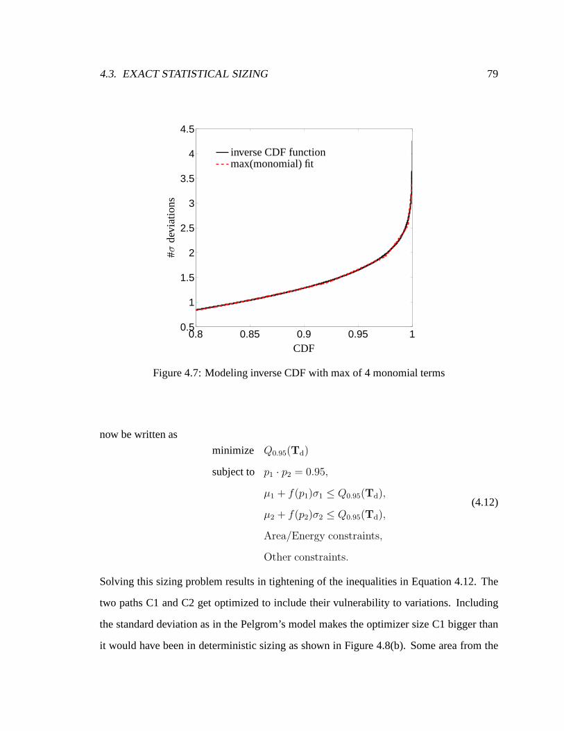
4.3. EXACT STATISTICAL SIZING 79
0.8 0.85 0.9 0.95 10.5
1
1.5
2
2.5
3
3.5
4
4.5
CDF
#σd
evia
tion
s
inverse CDF functionmax(monomial) fit
Figure 4.7: Modeling inverse CDF with max of 4 monomial terms
now be written as
minimize Q0.95(Td)
subject to p1 · p2 = 0.95,
µ1 + f(p1)σ1 ≤ Q0.95(Td),
µ2 + f(p2)σ2 ≤ Q0.95(Td),
Area/Energy constraints,
Other constraints.
(4.12)
Solving this sizing problem results in tightening of the inequalities in Equation 4.12. The
two paths C1 and C2 get optimized to include their vulnerability to variations. Including
the standard deviation as in the Pelgrom’s model makes the optimizer size C1 bigger than
it would have been in deterministic sizing as shown in Figure4.8(b). Some area from the

80 CHAPTER 4. OPTIMIZATION FOR ROBUSTNESS
bigger chain C2 is given to the smaller chain. The push back onµ(T1) andσ(T1) more than
compensates for the slight increase inµ(T2) andσ(T2) to give a betterQ0.95(Td). Figure
60 80 100 120 140 160 1800
10
20
30
40
50
delay in ps
dis
trib
utio
n
Q0.95(Td)
deterministicrobust
(a) Improvement in PDF
0 1 2 3 40
0.5
1
1.5
2
2.5
3
3.5
4
det. sizes (µm)
stat
.si
zes
(µm
)same size line
stat. sizes
(b) Size adjustment for robust design
Figure 4.8: Comparison of robust design to nominal design
4.8(a) shows the improvement in the PDF ofTd after statistical design. While the circuit is
now sized sub-optimally from a deterministic point of view,in presence of variations, the
statistics of the overall delay are dominated only by one of the paths. In circuits with many
outputs, more paths would be pushed back from being critical.
4.3.1 Balance of sensitivities
In the previous section, improvement in the mean delay of thesmaller chain makes up for its
relatively worse standard deviation to result in overallQ0.95(Td) improvement. While there
are many combinations of means and standard deviations thatcan give the sameQ0.95(Td),
under area constraints, the optimal choice is the one where the ratio of area sensitivity to
sensitivity of the delay metric (in this case,Q0.95(Td)), is the same for all the variables. We

4.3. EXACT STATISTICAL SIZING 81
can re-arrange the condition of optimality as
∂Q0.95(Td)∂µ1
∂A∂µ1
=
∂Q0.95(Td)∂µ2
∂A∂µ2
⇒∂Q0.95(Td)
∂µ1
∂Q0.95(Td)∂µ2
=∂A∂µ1
∂A∂µ2
(4.13)
whereA is the total area of the circuit. We cannot write this condition for Tnom in nomi-
nal design, asTnom is not differentiable inµ1,26. Now, for Q0.95(Td), the sensitivity ratio
changes with different combinations of means and standard deviations, but the equality
always remains7. To show this, let us consider a simpler version of the above circuit in
Figure 4.9. Assume that the loads on the two chains are unequal with some ratior, r > 1
C
rC
gnd
gnd
Figure 4.9: A simple circuit with symmetric structure but different loads
and for the gate delaysσ ∝ µ8. We will changer to see how the optimal area-delay point
moves with changing area distribution. Starting with nominal design we haveµ1 = µ2 and
so it follows thatσ1 = σ2. The load on path 1 is the larger of the two. Therefore, we can
redistribute the sizing between the two inverters such thatµ1 increases whileµ2 decreases
6This ratio is unity for increasingµ1,2, because if any path becomes slower, the delay is given by thatpath. The ratio is undetermined for decreasingµ1,2 because if any path becomes faster, then it no longerdetermines the circuit delay and its sensitivity becomes zero.
7assuming none of the variables hit their range limits8This is done to make the problem simpler by eliminating two variables

82 CHAPTER 4. OPTIMIZATION FOR ROBUSTNESS
keeping theQ0.95(Td) constant. Figure 4.10 shows the curve of constantQ0.95(Td) with
changing means obtained by taking many Monte-Carlo samplesin MATLAB. Clearly, in-
crease inµ1 causes greater and greater decrease inµ2 until theQ0.95 of the first path delay
itself equalsQ0.95(Td) at which point the curve becomes vertical.
0 0.05 0.1 0.15 0.2 0.25 0.3 0.350
0.1
0.2
0.3
0.4
0.5
0.6
0.7
0.8
0.9
1
increase inµ1 in #σ
dec
reas
einµ
2in
#σ
Figure 4.10: Tradeoff between mean delays for the sameQ0.95(Td)
While delay is inversely related to the size of the gates, area is directly proportional to
it. So with only sizing as our variable, we can write the totalcircuit area as
A = K(r/µ1 + 1/µ2),
whereK is some constant. Let us evaluate the area at every point on the constantQ95(Td)
curve and take the minimum, for different values of load ratio r. Figure 4.11 shows how
ther is same as the slope of the curve in Figure 4.10 at different points. If there are more

4.3. EXACT STATISTICAL SIZING 83
0 5 10 15 200
0.1
0.2
0.3
ratio of energy (r)
op
timal
incr
ease
inµ1
in#σ
Figure 4.11: Change in the optimal mean with the ratio of energy between the two chains
such parallel paths, the ratio of the sensitivities to area and Qα(Td) for all of them would
be equal. As a result some paths would be pushed back from being critical.
From this principle, we can infer that if all paths in a circuit are structurally identical
and drive the same load, then the optimal robust sizing will be no different from the deter-
ministic one, because given a fixed overall area every path will have the same sensitivity
to the overallQ0.95(Td), the same area cost, and therefore an equal share of the area as
any other path. Therefore one path cannot be pushed back fromthe other critical one. As-
suming that variations are size dependent, the only improvement can come from re-sizing
devices within a path to make the path delay distribution tighter.
4.3.2 Non-scalability of the exact solution
While the exact solution easily solves the robust design problem for inv52, it is not suitable
for typical circuits. For instance, for the circuit shown inFigure 4.12, which is a minor

84 CHAPTER 4. OPTIMIZATION FOR ROBUSTNESS
modification on inv52 circuit in Figure 4.6,T1 andT2 are not independent and so the95th
percentile boundary of their joint distribution cannot be given by the simple product of
gnd
gndin
Cload1
Cload2
Figure 4.12: A simple circuit with two dependent paths
probabilitiesp1 andp2. A more complicated constraint describing an ellipsoidal region is
needed. The situation gets even more complicated as the number of paths and the inter-
connections between them increase. We can see from Table 4.1that the number of paths in
circuit netlists grows exponentially with the size, makingit computationally impractical to
enumerate all the paths for robust sizing.
Another method to avoid enumerating all paths is to propagate delay PDFs throughout
the netlist in the same fashion as the static timing formulation in deterministic design.
However, as mentioned before, no practical family of distributions are closed under sum
andmax operations. Figure 4.13 shows an example of a nand gate with inputs having
gaussian distributions with comparable means but very different variance. The PDF of
the output timing shows a long tail which is hard to define witha set of few parameters,
especially as we care about the95th, a point that lies on this tail.
A simpler solution is therefore needed to capture variations during optimization. In the
following sections we describe our heuristics that get us most of the benefit of robust sizing

4.3. EXACT STATISTICAL SIZING 85
7 8 9 10 11 12 130
1
2
3
4
delay units
PD
FN(10, 1)N(10.1, 0.1)
(a) Two Gaussian path delays
9 10 11 12 13 14 150
0.2
0.4
0.6
0.8
1
1.2
delay units
PD
F
(b) delay at the converging node
Figure 4.13: Delay PDFs with comparable means but differentvariances produce long tailsat converging nodes
with only modest computational cost over deterministic sizing.
4.3.3 Previous work in robust sizing
The non-practicality of the exact solution for typical circuits led to a lot of research in the
area of sizing for robustness under variations [38, 73, 98, 31]. One idea involved aug-
menting the objective function in the deterministic sizingproblem to include a penalty for
outputs coming closer to the critical output [98], thereby reducing the number of critical
paths. The penalty coefficient had to be carefully chosen to prevent the optimizer from
choosing incorrect sizing to reduce the objective functionby focusing on the penalty in-
stead of the overall delay. Another path based approach [73]identifies the non-critical
paths responsible for the delay spread by defining adisutility function for gate and path
delays that includes both means and variances of the delay random variables. Sizing is
done to minimize thedisutility of non-critical paths responsible for timing yield loss. As
the algorithm has to enumerate paths, its complexity, and hence the solution time grows

86 CHAPTER 4. OPTIMIZATION FOR ROBUSTNESS
quickly with the circuit size. A simulation based approach using static delay formulation is
presented in [38] where approximate formulae are used to calculate the mean and variance
of the max of Gaussian distributions at every iteration. These formulae are complex to
solve and not amenable to analytical expressions. Besides,being non-convex, the conver-
gence is slow and approximating a distribution with a long tail as Gaussian is error-prone
as shown in Figure 4.13. Other algorithms [31] improve the delay statistics by adding area
to selectively upsize smaller devices. While this improvesthe delay statistics, increasing
area (energy) usually improves performance. The key is to improve performance with the
same area or energy constraint as that for the deterministicdesign.
4.3.4 Basic idea for robust sizing
Sizing problems generally have a broad “flat” region around the timing minima. This means
that in most cases small perturbations have small effects onthe nominal circuit delay. In
the deterministic method, the sizer puts most of the effort in getting to that lowest point in a
relatively flat region. But this design point might be very sensitive to variations because at
this point many paths are critical. In addition, many of these paths may be critical because
they contain small devices, which can increase the delay uncertainty. The idea is to get
robustness using these small sizing perturbations.
We can use two main insights from the exact statistical solution to formulate efficient
heuristics. Given a deterministically sized inv52 circuit, we saw in Section 4.3 how robust
sizing pushes back on one of the paths. This is the first thing we would like to achieve [98].
Secondly, if the uncertainty depends on the device size, then in addition to the pushing
back on paths, we need to adjust the device sizes within a to reduce the uncertainty. By
having a penalty for uncertainty that prevents the sizer from making bad choices about path
delays and device sizes, we might be able to achieve much of the benefit of considering the
4.4. HEURISTIC TECHNIQUES FOR ROBUST SIZING 87
complete distribution of the exact solution [69].
4.4 Heuristic techniques for robust sizing
Given that propagating accurate PDFs is impractical and modeling them as Gaussian causes
loss of information in the PDF tail, the key question is how topropagateQ0.95 of net tim-
ings. In addition, as many efficient means of solving the deterministic sizing problem have
been developed, is there a way to make the robust sizing look like the deterministic sizing
so that we can leverage the already existing solutions? To answer these questions, we seek
to modify the deterministic optimization problem to make itmore variation aware, while
maintaining the GP framework that allows efficient solutions. We propose the follow-
ing two techniques based on the performance bounds estimation methods using surrogate
netlists and the sensitivity analysis described in Sections 4.1.2 and 4.3.1 respectively.
4.4.1 Adding delay margins (ADM)
We propose to augment the gate delaysdi−o in (3.1) to obtaindi−o defined as
di−o = µ(di−o) + κjσ(di−o). (4.14)
The margin coefficientsκj introduced in Section 4.1.2 help to account for process variations
by adding to every gatej, a delay penalty term that is proportional to its delay uncertainty.
Margin coefficients provide the tradeoff between the mean and variance at the gate
level. The choice ofκ depends on what percentile of the distribution one is optimizing
for, but only weakly. This added margin is just a hint to the optimizer to try to minimize
uncertainty along critical paths. It is not a precise method. Section 4.1.2 described different

88 CHAPTER 4. OPTIMIZATION FOR ROBUSTNESS
choices ofκj that can be used for margining. Even if theQ0.95(Td) estimate at some given
κ is not good, a scaled value might help. In general it is hard topredict what value will
produce a result that is closest to the nominal delay (and hence to the optimal result as
nominal delay is a lower bound on theQ0.95(Td)). In fact, in our solution we try different
values ofκj and choose the value that yields the best result from SSTA using Monte Carlo
simulations. Useful values ofκ range from 1 to about 4. The region around minimum
Q0.95(Td) is flat so that with a granularity of 0.5, we can easily cover the entire range with
7 optimizations and SSTAs. The results of using this technique are presented in Section
4.5.
4.4.2 Using soft-max (USM) for merging path delays
SinceTout in Equation 3.1 is a maximum of a set of input delays that are random, the
distribution ofTout is shifted to the right of all the input delay distributions.This shift
is more pronounced when several of the input arrival time distributions are close to the
dominant one, and negligible when, say, only one of the inputs dominate the distribution.
To take into account the right shift caused by taking the maximum of a set of random
variables, we propose to use asoft maximumfunctionsmaxp defined as
smaxp(x) =(∑
|xi|p)1/p
,
wherep is the exponent that represents the penalty for closeness ofarguments and the
sum accounts for increase in uncertainty with every extra input. USM steers the optimizer
away from sizing many paths to be critical, a bad situation for delay statistics. While it
approaches themax function asymptotically, the soft max retains in spirit thefact that
under variations even a path with smaller nominal delay can contribute to the delay spread

4.4. HEURISTIC TECHNIQUES FOR ROBUST SIZING 89
at the converging node. To simulate the propagation ofQ0.95 of signal arrival times in the
netlist, USM is applied in conjunction with ADM.
USM is not only an enhancement to ADM, in some cases where ADM is ineffective, it
is necessary for robust sizing. For example, in the circuit presented in Section 4.3.1, with
σ(D) ∝ µ(D), ADM by itself just results in delay scaling without any sizing improvement
over the deterministic case. USM forces the paths to be unequal by modeling their pushing
effect on the overall delay PDF and leads to a better (not necessary optimal) distribution of
area between the two inverters.
Combining ADM and USM, we can write the equation forTout for the gate in Figure
3.2 by modifying Equation 3.1 as
Tout =( ∑
i=1,2,3
|Ti + Di−o|p)1/p
.
Using this relation as the delay propagation equation retains the computational merits of
the deterministic sizing problem (like sparsity), making the algorithm scalable to larger
circuits. Moreover, if theµ(di−o) andσ(di−o) of gate delays are generalized posynomials
then the problem can still be cast as a Generalized GeometricProgram (GGP) [10], leading
to efficient solutions. A crude search loop in the(p, κ) space around the basic optimiza-
tion routine can easily be implemented to obtain the best statistical sizing (as validated by
SSTA). In our experience the bestp varies over a range of 30 for different circuits depend-
ing on their topology. Within this range, the sensitivity ofQ0.95(Td) is small so that a
granularity of 10 suffices.

90 CHAPTER 4. OPTIMIZATION FOR ROBUSTNESS
4.4.3 Validating USM and ADM with two Gaussian delay variables
To show how ADM and USM together simulate the statistical delay propagation, let us
perform a simple MATLAB experiment. Consider two Gaussian random delay variables
R1 andR2. To keep the probability of negative samples negligible, let µ(R1) = 20 and
σ(R1) = 1 while we sweepµ(R2) from 15 to 25 andσ(R2) from 0.2 to 3. LetY =
max(R1,R2). We seek to modelQ0.84(Y) (i.e.the percentile corresponding to 1σ increase
over the mean) andQ0.95(Y) of the random variableY. We first find these values using
Monte Carlo simulation. These are plotted as solid curves ofvaryingµ(R2) for changing
values ofσ(R2) in Figures 4.14(a) and 4.15(a). We then defineQ0.84(Y) andQ0.95(Y) as:
Q0.84(Y ) = smaxp1(µ(Ri) + 1σ(Ri)), i = 1, 2
Q0.95(Y ) = smaxp2(µ(Ri) + 1.65σ(Ri)), i = 1, 2(4.15)
and attempt to fitQ0.84(Y) andQ0.95(Y) by choosing the rightp. The model fit is shown
in dashed curves. The values ofκ must be equal toΦ−1(0.84) = 1 andΦ−1(0.95) =
1.65 in order to fit the asymptotic regions where one distributioncompletely dominates the
other. The values ofp (p1 andp2 in Equation 4.15) change to represent how smoothly
the percentile lines curve, as shown in Figures 4.14(b) and 4.15(b). The plots in Figures
4.14 and 4.15 show that oursmaxp andκσ margins give close estimates of theQ0.84(Y)
andQ0.95(Y) for specific values ofp andκ. HereR1 andR2 represent the delay of two
converging paths which can vary over a significant range fromeach other in their mean and
standard deviation. The value ofp decreases as the extent of variations increases, reflecting
a higher penalty for paths with high variance coming closer.
For simplicity, we use uniformp andκ for all gates in the circuit. As mentioned before,
in practice, a range of 30 suffices forp. Values ofp exceeding the range are associated with
relatively small variations that do not dominate the overall delay. This range is chosen from
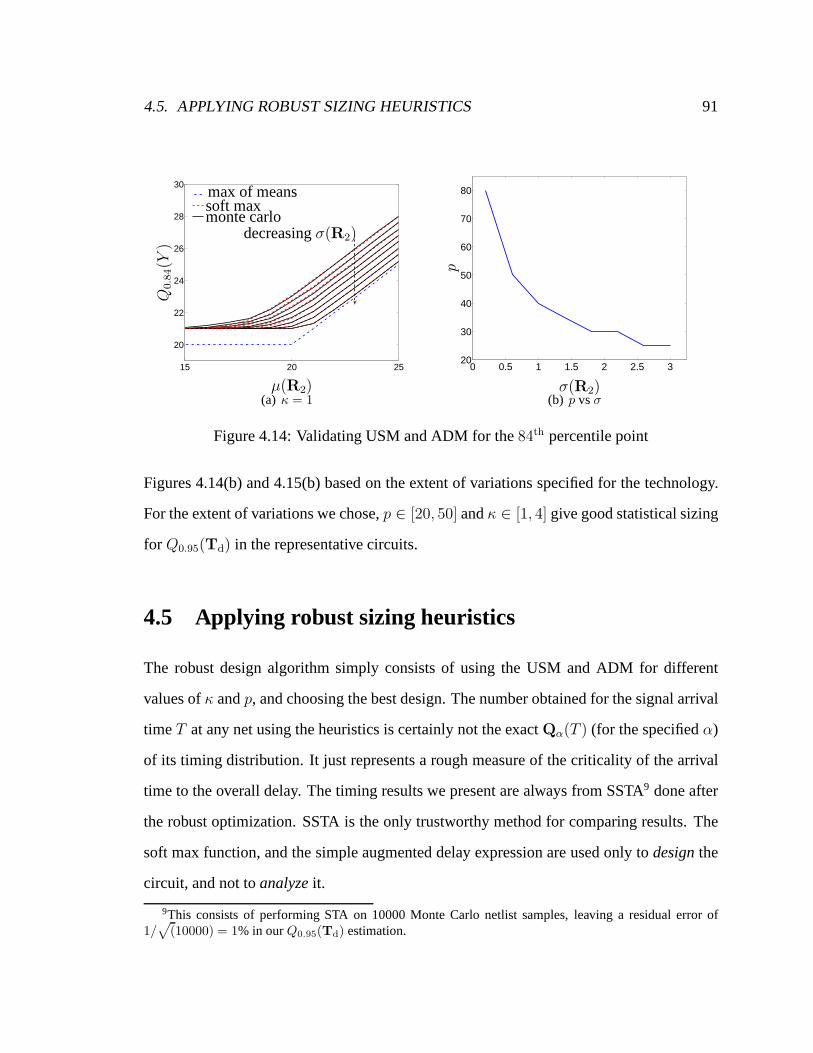
4.5. APPLYING ROBUST SIZING HEURISTICS 91
15 20 25
20
22
24
26
28
30
µ(R2)
Q0.8
4(Y
)
max of meanssoft maxmonte carlo
decreasingσ(R2)
(a) κ = 1
0 0.5 1 1.5 2 2.5 320
30
40
50
60
70
80
σ(R2)
p
(b) p vsσ
Figure 4.14: Validating USM and ADM for the84th percentile point
Figures 4.14(b) and 4.15(b) based on the extent of variations specified for the technology.
For the extent of variations we chose,p ∈ [20, 50] andκ ∈ [1, 4] give good statistical sizing
for Q0.95(Td) in the representative circuits.
4.5 Applying robust sizing heuristics
The robust design algorithm simply consists of using the USMand ADM for different
values ofκ andp, and choosing the best design. The number obtained for the signal arrival
timeT at any net using the heuristics is certainly not the exactQα(T ) (for the specifiedα)
of its timing distribution. It just represents a rough measure of the criticality of the arrival
time to the overall delay. The timing results we present are always from SSTA9 done after
the robust optimization. SSTA is the only trustworthy method for comparing results. The
soft max function, and the simple augmented delay expression are used only todesignthe
circuit, and not toanalyzeit.
9This consists of performing STA on 10000 Monte Carlo netlistsamples, leaving a residual error of1/
√(10000) = 1% in ourQ0.95(Td) estimation.

92 CHAPTER 4. OPTIMIZATION FOR ROBUSTNESS
15 20 25
20
22
24
26
28
30
µ(R2)
Q0.9
5(Y
)
(a) κ = Φ−1(0.95) = 1.65
0 0.5 1 1.5 2 2.5 3
30
40
50
60
70
80
90
σ(R2)
p(b) p reduces withσ(R2)
Figure 4.15: Validating USM and ADM for the95th percentile point
For testing the efficacy of our heuristics, we assume a general dependence of delay
variation on transistor size given as
σ(D)
µ(D)∝ 1
(LW )α, α ≥ 0, (4.16)
whereα is the degree of dependence on size. For Pelgrom’s model,α = 0.5. Here we
show the results forα = 0.5 andα = 0. The variation in both cases is normalized to have
15% of relative standard deviation in the drive current (σ(Id)/Id) for 1µ minimum length
device.
Figure 4.16 shows the delay distribution improvement for 32-bit adder after using the
ADM and USM techniques assuming Pelgrom’s variation model.TheQ0.95(Td) improves
by more than 20% over the deterministic design. The reason for this improvement becomes
clear by observing theµ-σ scatter plot for this design shown in Figure 4.17. The high
variance critical paths resulting from deterministic sizing are pushed back from dominating
the overall delay, at the cost of modest increase in the delay(and variance) of the low
variance paths, resulting in overall reduction ofQ0.95(Td). The total area is redistributed

4.5. APPLYING ROBUST SIZING HEURISTICS 93
0.75 0.8 0.85 0.9 0.95 1 1.05 1.1 1.150
5
10
15
20
25
30
35
40
Tcycle in ns
dis
trib
utio
n
deterministic sizing
robust sizing
Figure 4.16: Improvement inQ0.95(Td) for a 32-bit LF adder usingκ = 1.5 andp = 30
to upsize the high variance paths. The heuristics seek to achieve the optimality condition
described in Section 4.3.1 by balancing the sensitivity ofQ0.95(Td) to different path delays
with their marginal cost of area. The delay of the circuit is now dominated by a fewer
critical paths.
Table 4.2 shows the results of using our heuristics on the benchmark circuits introduced
in Section 4.1.2. To get an upper bound on the sub-optimalityof our solution, we use
Tnom as our lower bound estimate onQ0.95(Td). This upper bound is shown in the last
column. Note that we cannot use the tighter lower bound described in Section 4.1.2 for sub-
optimality calculation as we do not have the optimal sizing to begin with. Results shows
that using ADM and USM heuristics combined give an improvement of anywhere from 0
to 24% ofTnom depending on the netlist topology. Due to inherent structural symmetry, the
decoder dec8-256, 32 bit logarithmic shifter/rotator sh32and single error correction (SEC)

94 CHAPTER 4. OPTIMIZATION FOR ROBUSTNESS
0.3 0.4 0.5 0.6 0.7 0.820
40
60
80
100
120 Deterministic sizing
0.3 0.4 0.5 0.6 0.7 0.820
40
60
80
100
120 Robust sizing
µ(Tpath) in ns
σ(T
path
)in
ps
µ(Tpath) in ns
σ(T
path
)in
ps
Figure 4.17:µ–σ scatter plot for all paths of 32bit LF adder (Tpath = path delay)
circuits c1355 and c499 have many of theirQ0.95(Td) equally sensitive to many of their
paths and consequently show very small statistical improvement over deterministic sizing.
In particular, the improvement in decoders is strictly due to redistribution of width within a
single path (like the inv5 circuit). Naturally, lesser improvement over deterministic sizing
means higher sub-optimal bound. Even circuits with identical logical function (add32KS,
add32BK and add32Sk) can have different improvements basedon their topologies. While
add32KS has many paths of similar length, add32BK has a single long path with many
small side paths. In deterministic sizing, the optimizer downsizes many of these side paths
making them critical. These small paths suffer from large variability. Consequently, under
identical design constraints,Q0.95(Td) degrades the most for add32BK under variations.

4.5. APPLYING ROBUST SIZING HEURISTICS 95
Table 4.2: SSTA of robust sizing using Pelgrom’s model. Delays are in FO4. The originalQ0.95(Td) is for deterministic sizing.
circuits orig. Tnom unif. UK + κ ∝ KSq + imprvmnt maxQ0.95(Td) κ smax() 1√
lismax() in Q0.95(Td) subopt
UK KSq in % Tnom in % Tnom
inv5 8.3 7.4 7.5 7.5 7.5 7.5 10 3inv52 5 4.3 4.6 4.6 4.7 4.6 9 8
dec8-256 17.3 15.3 17.3 17.3 17.3 17.3 0 13sh32 19 16 18.4 18.3 18.4 18.3 4 14
add32KS 17.7 13.3 16.1 15.4 15.7 15.4 18 15add32BK 17.2 12.9 14.5 14.2 14.2 14.2 24 10add32Sl 16.7 13.1 15.1 14.9 15.1 14.9 14 14c1355 22.9 20 22.4 22.1 22.2 22.1 4 10c1908 30.7 25.8 30 28.3 28.9 28.3 9 9c2670 22.8 17.6 20.3 18.6 19 18.6 24 6c3540 34.1 27.7 32.2 30.1 30.3 30.1 15 9c432 22.6 17.8 20.2 19 19 19 20 7c499 18.1 15.8 17.9 17.6 17.8 17.6 3 11c5315 32.9 26.7 29.3 28.4 28.4 28.3 17 6c7552 35.8 30.5 33 32.2 32.4 32.2 12 5c880 23.2 18.3 19.8 19.3 19.5 19.3 21 5
However, this also means that add32BK stands to gain the mostfrom statistical sizing.
The heuristics prevent the side paths from being downsized to criticality while maintaining
a reasonable overall delay. As expected, add32KS gains the least because of having a
more uniform topology. The topology of add32Sk falls in the middle of the two extremes.
However, under identical design constraints, Sklansky topology still wins as it achieves the
smallestTnom that makes up for its poorer gains from statistical design due to its topology
Table 4.3 show similar results for the case whereσ(Id) ∝ µ(Id). In this case, because
the variations for two stages with equal relative loading isthe same regardless of the driver
size, having small devices is not bad. The improvement inQ0.95 thus comes only from
sizing the paths relative to one another, which is clear fromgetting no improvement in the

96 CHAPTER 4. OPTIMIZATION FOR ROBUSTNESS
inv5 benchmark. Exact statistical sizing on inv5 and inv52 also shows negligible improve-
ment in robustness. In fact, using uniform margin coefficients for ADM without USM
is ineffective as it just scales the delay model and hence results in deterministic sizing10.
Here we rely largely on USM to get us the robust design. The statistical behavior of ALU
Table 4.3: Results of robust sizing techniques in case whereσ ∝ µ. Delays are in FO4.
circuits det. Tnom unif. UK + κ ∝ KSq + imprvmnt suboptQ0.95(Td) κ smax() 1/
√li smax() in Q0.95(Td) u. bound
UK KSq in % Tnom in % Tnom
inv5 8.3 7.4 8.3 8.3 8.3 8.3 0 12inv52 5 4.3 5 4.8 5 4.8 3 14
dec8-256 18.8 15.3 18.8 18.8 18.8 18.8 0 23sh32 19.6 16 19.6 19.4 19.6 19.4 1 21
add32KS 16 13.3 16 15.5 16 15.5 4 16add32BK 15.3 12.9 15.3 14.5 15.3 14.5 6 13add32Sl 16 13.1 16 15.3 16 15.3 5 17c1355 22.3 20 22.3 22 22.3 22 1 10c1908 29 25.8 29 28.1 29 28.1 3 9c2670 21 17.6 21 18.9 20.9 18.9 12 7c3540 31.9 27.7 31.9 30.3 31.9 30.3 6 9c432 20.8 17.8 20.8 19.5 20.8 19.5 7 10c499 17.8 15.8 17.8 17.6 17.8 17.6 1 11c5315 31.4 26.7 31.4 28.9 31.4 28.9 9 8c7552 34.8 30.5 34.8 32.7 34.8 32.7 7 7c880 20.7 18.3 20.7 19.8 20.6 19.8 5 8
and control logic benchmark c2670 is governed mainly by having many really short paths
along with really long ones11. Therefore it shows marked improvements over deterministic
design in both variation cases .
We can see from Eq. 4.16 that the absolute variation in delay,represented byσ(D),
increases with lowering the size of the effective driver transistor or increasing the delay of
10In fact, this is nothing but using some worst case corner, as defined by theκ value, which naturally doesno change the sizing.
11Here short and long is based on the number of stages

4.6. INCLUDING VARIATIONS IN ENERGY 97
that stage. Therefore a simple method to curb variations is to limit the minimum device
size in deterministic sizing so that all devices are sized away the portion where1/√
size
is high. The disadvantage of this simple method is that it uniformly constraints all devices
without considering the sensitivity of the overall delay totheir delay variation. An alterna-
tive simple method is to constraint the delay per stage in deterministic sizing. This would
keep the non-critical but otherwise highly variation-prone paths well sized. Again, this
method has the disadvantage of constraining all stages uniformly to over size even statisti-
cally non-dominant stages. The ADM and USM techniques effectively include both these
techniques by upsizing and improving the delay only the statistically dominant stages as
indicated by the sensitivity ofQ0.95(Td) to the delay variation of different stages.
4.6 Including variations in energy
While accounting for delay variations is made complicated by the sum and max operations,
the total energy is simply the sum of energy dissipated in every gate and interconnect. As
the number of these elements is usually quite large, the PDF of the total energy dissipation
is quite narrow for local independent variations and its mean is a good estimate for the
energy of the circuit. Dynamic energy is the sum of energy dissipated in all the switching
capacitors (Equation 2.3). Assuming 10% local temporal variations inVdd, we useµ(V 2dd)
in our expressions. Note that this value is bigger thanµ2(Vdd).
µ(V 2dd) = µ2(Vdd) + σ2(Vdd)
for Gaussian distribution ofVdd. The local variations in individualCis are averaged out by
summing over a large number of gates.
Just like calculating the correctµ(V 2dd) for dynamic energy, care should be taken to

98 CHAPTER 4. OPTIMIZATION FOR ROBUSTNESS
calculate the correct average leakage energy. Assuming that Vth in Equation 2.6 has a
Gaussian distribution,Ij has a log-normal distribution and its average value is greater than
that obtained by usingµ(Vth) in (2.6) as shown below [43].
µ(Ij) = I0 exp(−µ(Vth,j) − γDVdd
nVT
+σ2(Vth,j)
2(nVT )2) (4.17)
In other words, the mean of leakage current is increased by a factorFleak given as
Fleak = exp(σ2(Vth)
2(nVT )2).
Clearly,Fleak increases exponentially with the variation inVth. The effect ofVth variation
on the transistor leakage current is shown in Figure 4.18. The dependence ofσ2(Vth) on
sizing through Pelgrom’s model causesFleak to shoot up as the devices get smaller. The
same plot also compares the average leakage current in the presence of variations (4.17)
to the nominal value usingVth fixed to its mean, as a function of transistor width. The
currents are normalized to the nominal leakage current of a1µ wide transistor. Interestingly,
due to variations, as the width reduces, the average leakagedoes not get smaller, in fact,
it can actually increase! At larger widthsFleak approaches unity and hence the average
leakage asymptotically reaches the nominal value. This canbe viewed as lowering of the
effective threshold voltage for leakage in presence of variations. The DIBL factor term
can be adjusted similarly for local variations inVdd. Fleak can be as high as 6 or 7 for
smaller devices. In a deterministic approach, the optimizer, unaware of this factor, sets
many devices to have small sizes and lowVth to obtain a good drive with lower input
capacitance. This is bad as the highσ(Vth) for small devices exponentially increases the
leakage current, contrary to the assumptions made by the deterministic optimizer.
With the inclusion ofVth andVdd as design variables, we can expressσ(Id) as a function

4.6. INCLUDING VARIATIONS IN ENERGY 99
0 0.5 1 1.5 2 2.5 3 3.5 4 4.5 50
1
2
3
4
5
6
0 0.5 1 1.5 2 2.5 3 3.5 4 4.5 51
2
3
4
5
6
7
Width in µ
No
rmal
ized
µ(I
j)
Fle
ak
Fleak
statisticalµ(Ij)
nominalIj
Figure 4.18:Fleak and normalizedµ(Ij) (4.17) as a function of transistor width
of variations inVth and the current factorβ [70]. For simplicity we modelσ(Id) based on
the alpha power law current model [76] as
σ2(Id)
I2d
=σ2(Vth)
V 2od
+σ2(β)
β2
whereσ2(β) accounts for variation inβ due to variations in channel length, mobility etc..
We assume that these these two sources of variations are independent. Using Pelgrom’s
model we can express the local variation inVth for a stack of transistors as
σ2(Vth) ∝ 1
LeffWeff.
The relative variation inβ also has the same dependence. The quadratic model is made
only to formulateσ(Id) and produces a small error in calculating delay variation which is

100 CHAPTER 4. OPTIMIZATION FOR ROBUSTNESS
calculated from Equation 2.7 as
σ(τd) =dτd
dId
σ(Id).
Using the above equations andVth, Vdd and sizing as design variables, we can obtain the
6 8 10 12 14 16 18 20 220
0.5
1
1.5
2
2.5
3
3.5
4
4.5
delay in FO4
ener
gy
inp
J
deterministic design
robust designVdd,Vth and sizing
Vdd,Vth and sizing
8%
Figure 4.19: Improvement in the energy-delay tradeoff curve for the95th percentile delaydue to statistical design
Q0.95 energy-delay tradeoff curves for different circuits. Figure 4.19 shows a minimum of
8% improvement in the energy-delay tradeoff curve forQ0.95(Td) of a 32bit adder. The
improvement at the higher delay side is mainly due to curbingdelay variations from device
sizing, while the gain at the higher energies is mainly from includingVth variations in
estimating leakage energy.
4.7. SUMMARY 101
4.7 Summary
Process variations cause uncertainties in gate delays which lead to uncertainty in the overall
delay of the circuit. Calculating the complete PDF or a percentile point of the overall delay
precisely is difficult, but upper and and lower bounds of a particular percentile point can
be efficiently calculated by performing STA on surrogate netlists using additional margins
on individual gate delays. Monte Carlo methods can also be used to estimate the PDF and
percentile points.
Deterministic sizing results into many equally critical paths which is statistically worse
for delay. The optimizer downsizes many of these paths to contain smaller gates which,
according to Pelgrom’s model, exhibit larger delay uncertainty and significantly increase
the delay variance of that path and thus the overall delay. For robustness against process
variations, the correct problem to solve is to minimize someα percentile of the overall
delay (Qα(Td)) rather than minimizing the nominal delay. In this case the optimizer will
distribute the resources (area or energy) between different paths, and different gates within
a path, such that the ratio of sensitivity ofQα(Td) to sensitivity of area or energy is the
same for all gate delays.
While the exact formulation of this statistical design problem is possible for a few
simple circuits, it is extremely tedious for most circuits.However, the optimizer just needs
to be prevented from making bad choices of making many paths critical and downsizing
gates in the process. The two heuristic techniques described in this chapter – of addingσ
delay margins to gate delay expressions and using soft max function to combine path delays
at converging nodes – are effective in designing robust circuits by steering the optimizer
to push back on non-critical paths and avoid small devices inpaths dominating the overall
delay. Thus, no propagation of delay PDFs is required and similar to the deterministic
sizing, the statistical sizing problem can be cast as a GP, with modest overhead.

102 CHAPTER 4. OPTIMIZATION FOR ROBUSTNESS
Results of applying these heuristics show that the improvement in robustness depends
strongly on the topology. Circuits with many structurally identical paths benefit less from
statistical design as no path delay can be traded with another for sizing. The bigger the
asymmetry among the logical paths in the netlist, the largeris the benefit of statistical
design over deterministic one.
As energy is the sum of many terms, sum of the average energiesfor all gates and nets
is a good estimate for the overall energy. However, leakage energy increases exponentially
with decreasingVth and hence is statistically dominated by the lowVth devices. Therefore,
the average leakage is not the leakage of an average device, the variance ofVth – which
depends inversely on device size –also affects the value. Asthis variation depends on
sizing, we can steer the optimizer away from using highly leaky devices that will degrade
the energy of the circuit. Using the proposed heuristic techniques of statistical sizing with
the correct estimate of energy give a robust design having a much better energy-delay
tradeoff curve under process variations.

Chapter 5
Conclusions
With high end microprocessors facing steep cooling costs and rising demands for longer
battery life in portable devices, energy-efficiency is crucial in digital systems today. For
energy-efficiency, the ratios of marginal cost (or sensitivity) of delay and energy to all the
user tunable design variables – sizing,Vdd, Vth, logic style and topology should be equal,
so that no variable can be traded off with another for a betterdesign. For continuous vari-
ables, like sizing,Vdd andVth, the circuit design problem can be formulated as a Geometric
Program, which can be solved very efficiently. The Stanford Circuit Optimization Tool
facilitates schematic design entry, automatic problem formulation and post-optimization
timing analysis. We used this tool to generate optimal designs for different topologies and
logic styles of a 32-bit adder, which served as our case study. By overlapping the different
tradeoff curves we generated the overall energy-delay tradeoff curve for 32-bit addition
spanning a range of 60x in energy and 10x in delay. This curve not only allows designers
to find the best design for given specifications, but also provides the information about the
energy and delay costs (or gains) involved in changing to a different specification.
With shrinking feature size, local random process variations are becoming increasingly
103

104 CHAPTER 5. CONCLUSIONS
detrimental to circuit performance. While the goal should be to optimize for the efficiency
of circuits that are actually produced, in fact, ignoring process variations by using fixed
parameters during optimization can actually make the design more vulnerable to process
variations. Making all paths critical, which is the optimalcondition for deterministic sizing,
pushes out the overall delay under variations. At the same time, ignoring the exponential
dependence of leakage energy onVth results into designs that consume excessive static
power after fabrication.
For an optimal statistical solution that results in a robustdesign, the ratio of sensitivities
of a specified percentile delay point (as opposed to nominal delay) and energy should be
made equal for all the design variables. We show that this problem can be solved exactly
for certain circuit topologies for some distributions. However, it is impractical to solve for
most typical circuits. Instead, simple heuristics can be used to get most of the benefit of
statistical sizing. We have developed two heuristics that effectively include process vari-
ations during optimization and approximately solve the statistical design problem for all
topologies. We add standard deviation margins to the mean delay model used in determin-
istic sizing and use “softmax”, instead ofmax() to combine delays at converging nodes.
Unlike deterministic sizing, these heuristics effectively target two aspects of a robust design
– resizing stages with high delay uncertainty within the critical paths, and pushing back on
paths that need not be critical and/or have a high delay variance.
Because the total energy is a sum of many varying terms, the average total energy is
a relatively good estimate of the overall energy. However due to nonlinear dependence of
dynamic energy onVdd and leakage energy onVth, the average energy is not the same as
the energy calculated with average values ofVdd andVth. It depends on the variations in
these parameters. These variations add a factor that must beconsidered to determine the
correct estimate of energy in statistical optimization.

5.1. FUTURE WORK 105
The proposed heuristic method for designing robust energy-efficient circuits largely
retains the original GP formulation for deterministic design problem so we can still leverage
the benefit of efficient GP solutions. The extent to which a given circuit can be made robust
is highly dependent on its topology. For structurally symmetric circuits like the decoder,
the robust design is same as the nominal design, while for designs where there is a large
disparity in sensitivities, either due to different numberof stages in different paths, or
different loads at different outputs, the improvement can be up to 30% assuming Pelgrom’s
model for variations.
5.1 Future work
The idea of balancing the ratio of marginal energy-delay cost across all design variables can
be used at other levels of design hierarchy to create energy-efficient systems. In particular,
at the micro-architecture level, it can be used to allocate the optimal amount of energy
to different functional units, cache, load-store units andso on depending on their marginal
costs to the overall performance and energy of the system. SCOT enables us to generate the
Pareto-optimal E-D tradeoff curves of different circuit blocks. These curves can be used in
another tool that takes in the architecture and optimizes for different performance-energy
points. Work is ongoing in our group to develop architecturelevel energy-performance
models that enable design of energy-efficient systems usingthe energy-delay models for
different circuit blocks [3]. A similar approach can be usedto design devices aimed for a
particular circuit requirement. An example for BJTs is presented in Ref. [41].
Ensuring a particular overall parametric yield involves a statistical design methodol-
ogy that deals with all the three different kinds of variations, namely, global chip-to-chip,
correlated within-chip and local random variations. As discussed in Section 2.3, design

106 CHAPTER 5. CONCLUSIONS
techniques exist for dealing with the first two. This thesis focused on designing robust cir-
cuits for local random variations. The next step is to generate a complete statistical solution
by integrating the proposed algorithms in the existing design flow.

Appendix A
Geometric programming basics
The following material is taken from Ref. [9].
A.1 Monomial and posynomial functions
Let x1, . . . , xn denoten real positive variables, andx = (x1, . . . , xn) a vector with compo-
nentsxi. A real valued functionf of x, with the form
f(x) = cxa1
1 xa2
2 · · ·xan
n , (A.1)
wherec > 0 andai ∈ R, is called amonomial function, or more informally, amonomial
(of the variablesx1, . . . , xn). We refer to the constantc as thecoefficientof the monomial,
and we refer to the constantsa1, . . . , an as theexponentsof the monomial. As an example,
2.3x21x
−0.152 is a monomial of the variablesx1 andx2, with coefficient2.3 andx2-exponent
−0.15.
Any positive constant is a monomial, as is any variable. Monomials are closed under
multiplication and division: iff andg are both monomials then so arefg andf/g. (This
107

108 APPENDIX A. GEOMETRIC PROGRAMMING BASICS
includes scaling by any positive constant.) A monomial raised to any power is also a
monomial:
f(x)γ = (cxa1
1 xa2
2 · · ·xan
n )γ = cγxγa1
1 xγa2
2 · · ·xγan
n .
The term ‘monomial’, as used here (in the context of geometric programming) is similar
to, but differs from the standard definition of ‘monomial’ used in algebra. In algebra,
a monomial has the form (A.1), but the exponentsai must be nonnegative integers, and
the coefficientc is one. Throughout this thesis, ‘monomial’ refers to the definition given
above, in which the coefficient can be any positive number, and the exponents can be any
real numbers, including negative and fractional.
A sum of one or more monomials,i.e., a function of the form
f(x) =K∑
k=1
ckxa1k
1 xa2k
2 · · ·xankn , (A.2)
whereck > 0, is called aposynomial functionor, more simply, aposynomial(with K terms,
in the variablesx1, . . . , xn). The term ‘posynomial’ is meant to suggest a combination of
‘positive’ and ‘polynomial’.
Any monomial is also a posynomial. Posynomials are closed under addition, multipli-
cation, and positive scaling. Posynomials can be divided bymonomials (with the result
also a posynomial): Iff is a posynomial andg is a monomial, thenf/g is a posynomial.
If γ is a nonnegative integer andf is a posynomial, thenfγ always makes sense and is a
posynomial (since it is the product ofγ posynomials).
Let us give a few examples. Supposex, y, andz are (positive) variables. The functions
(or expressions)
2x, 0.23, 2z√
x/y, 3x2y−.12z

A.2. STANDARD FORM GEOMETRIC PROGRAM 109
are monomials (hence, also posynomials). The functions
0.23 + x/y, 2(1 + xy)3, 2x + 3y + 2z
are posynomials butnot monomials. The functions
−1.1, 2(1 + xy)3.1, 2x + 3y − 2z, x2 + tan x
are not posynomials (and therefore, not monomials).
A.2 Standard form Geometric Program
A geometric program(GP) is an optimization problem of the form
minimize f0(x)
subject to fi(x) ≤ 1, i = 1, . . . , m,
gi(x) = 1, i = 1, . . . , p,
(A.3)
wherefi are posynomial functions,gi are monomials, andxi are the optimization variables.
(There is an implicit constraint that the variables are positive, i.e., xi > 0.) We refer to the
problem (A.3) as a geometric program instandard form, to distinguish it from extensions
we will describe later. In a standard form GP, the objective must be posynomial (and it
must be minimized); the equality constraints can only have the form of a monomial equal
to one, and the inequality constraints can only have the formof a posynomial less than or
equal to one.

110 APPENDIX A. GEOMETRIC PROGRAMMING BASICS
As an example, consider the problem
minimize x−1y−1/2z−1 + 2.3xz + 4xyz
subject to (1/3)x−2y−2 + (4/3)y1/2z−1 ≤ 1,
x + 2y + 3z ≤ 1,
(1/2)xy = 1,
with variablesx, y andz. This is a GP in standard form, withn = 3 variables,m = 2
inequality constraints, andp = 1 equality constraints.
We can switch the sign of any of the exponents in any monomial term in the objective
or constraint functions, and still have a GP. For example, wecan change the objective in
the example above tox−1y1/2z−1 + 2.3xz−1 + 4xyz, and the resulting problem is still a
GP (since the objective is still a posynomial). But if we change the sign of any of the
coefficients, or change any of the additions to subtractions, the resulting problem is not a
GP. For example, if we replace the second inequality constraint with x + 2y − 3z ≤ 1, the
resulting problem isnot a GP (since the lefthand side is no longer a posynomial).
A.2.1 Simple extensions of GP
Several extensions are readily handled. Iff is a posynomial andg is a monomial, then the
constraintf(x) ≤ g(x) can be handled by expressing it asf(x)/g(x) ≤ 1 (sincef/g is
posynomial). This includes as a special case a constraint ofthe formf(x) ≤ a, wheref
is posynomial anda > 0. In a similar way ifg1 andg2 are both monomial functions, then
we can handle the equality constraintg1(x) = g2(x) by expressing it asg1(x)/g2(x) = 1
(sinceg1/g2 is monomial). We can maximize a nonzero monomial objective function, by
minimizing its inverse (which is also a monomial).
A.3. GENERALIZATION 111
As an example, consider the problem
maximize x/y
subject to 2 ≤ x ≤ 3,
x2 + 3y/z ≤ √y,
x/y = z2,
(A.4)
with variablesx, y, z ∈ R (and the implicit constraintx, y, z > 0). Using the simple
transformations described above, we obtain the equivalentstandard form GP
minimize x−1y
subject to 2x−1 ≤ 1, (1/3)x ≤ 1,
x2y−1/2 + 3y1/2z−1 ≤ 1,
xy−1z−2 = 1.
It’s common to refer to a problem like (A.4), that is easily transformed to an equivalent GP
in the standard form (A.3), also as a GP.
A.3 Generalization
In this section we describe extensions of GP that are less obvious than the simple ones
described in Section A.2.1. This leads to the idea ofgeneralized posynomials, and an
extension of Geometric Programming calledGeneralized Geometric Programming.
We say that a functionf of positive variablesx1, . . . , xn is ageneralized posynomialif
it can be formed from posynomials using the operations of addition, multiplication, positive
(including fractional) power, and maximum.

112 APPENDIX A. GEOMETRIC PROGRAMMING BASICS
Let us give a few examples. Supposex1, x2, x3 are positive variables. The function
max{1 + x1, 2x1 + x0.2
2 x−3.93
}
is a generalized posynomial, since it is the maximum of two posynomials. The function
(0.1x1x
−0.53 + x1.7
2 x0.73
)1.5
is a generalized posynomial, since it is the positive power of a posynomial. All of the
functions appearing in the examples of the two previous sections, as the objective or on the
lefthand side of the inequality constraints, are generalized posynomials.
As a more complex example, the function
h(x) = (1+max{x1, x2})(max
{1 + x1, 2x1 + x0.2
2 x−3.93
}+
(0.1x1x
−0.53 + x1.7
2 x0.73
)1.5)1.7
is a generalized posynomial. This can be seen as follows:
• x1 andx2 are variables, and therefore posynomials, soh1(x) = max{x1, x2} is a
generalized posynomial.
• 1+x1 and2x1+x0.22 x−3.9
3 are posynomials, soh2(x) = max{1 + x1, 2x1 + x0.2
2 x−3.93
}
is a generalized posynomial.
• 0.1x1x−0.53 + x1.7
2 x0.73 is a posynomial, soh3(x) =
(0.1x1x
−0.53 + x1.7
2 x0.73
)1.5is a
generalized posynomial.
• h can be expressed ash(x) = (1 + h1(x)) (h2(x) + h3(x))1.7 (i.e., by addition, mul-
tiplication, and positive power, fromh1, h2, andh3) and therefore is a generalized
posynomial.

A.3. GENERALIZATION 113
Generalized posynomials are by definition, closed under addition, multiplication, posi-
tive powers, and maximum, as well as other operations that can be derived from these, such
as division by monomials. They are also closed under composition in the following sense.
If f0 is a generalized posynomial ofk variables, for which no variable occurs with a nega-
tive exponent, andf1, . . . , fk are generalized posynomials, then the composition function
f0(f1(x), . . . , fk(x))
is a generalized posynomial.
A very important property of generalized posynomials is that they satisfy the log con-
vexity property that posynomials satisfy. Iff is a generalized posynomial, the function
F (y) = log f(ey)
is a convex function: for anyy, y, and anyθ with 0 ≤ θ ≤ 1, we have
F (θy + (1 − θ)y) ≤ θF (y) + (1 − θ)F (y).
In terms of the original generalized posynomialf and variablesx and x, we have the
inequality
f(xθ1x
1−θ1 , . . . , xθ
nx1−θn ) ≤ f(x1, . . . , xn)θf(x1, . . . , xn)1−θ,
for anyθ with 0 ≤ θ ≤ 1.

114 APPENDIX A. GEOMETRIC PROGRAMMING BASICS
A.3.1 Generalized geometric program
A generalized geometric program(GGP) is an optimization problem of the form
minimize f0(x)
subject to fi(x) ≤ 1, i = 1, . . . , m,
gi(x) = 1, i = 1, . . . , p,
(A.5)
whereg1, . . . , gp are monomials andf0, . . . , fm are generalized posynomials. Since any
posynomial is also a generalized posynomial, any GP is also aGGP.
While GGPs are much more general than GPs,they can be mechanically converted to
equivalent GPs[10] As a result, GGPs can be solved very reliably and efficiently, just like
GPs. The conversion from GGP to GP can be done automatically by a parser as it parses
the expressions describing the problem. The GP modeler onlyneeds to know the rules for
forming a valid GGP, which are very simple to state. There is no need for the user to ever
see, or even know about, the extra variables introduced in the transformation from GGP to
GP.
Unfortunately, the name ‘generalized geometric program’ has been used to refer to
several different types of problems, in addition to the one above. For example, some authors
have used the term to refer to what is usually called asignomial program1, a very different
generalization of a GP, which in particular cannot be reduced to an equivalent GP, or easily
solved.
Once we have the basic idea of a parser that scans a problem description, verifies that
it is a valid GGP and transforms it to GP form (for numerical solution), we can add several
1A signomial is a function with the same form as a posynomial (i.e., (A.2), where the coefficientscj areallowed to be negative. A signomial program (SGP) is a generalization of a geometric program, which hasthe form of a GP, but the objective and constraint functions can be signomials
A.3. GENERALIZATION 115
useful extensions. The parser can also handle inequalitiesinvolving negative terms in ex-
pressions, negative powers, minima, or terms on the righthand side of inequalities, in cases
when they can be transformed to valid GGP inequalities. For example, the inequality
x + y + z − min{√xy, (1 + xy)−0.3} ≤ 0 (A.6)
(which is certainly not a valid generalized posynomial inequality) could be handled by a
parser by first replacing the minimum with a variablet1 and twoupper bounds, to obtain
x + y + z − t1 ≤ 0, t1 ≤√
xy, t1 ≤ (1 + xy)−0.3.
Moving terms around (by adding or multiplying) we obtain
x + y + z ≤ t1, t1 ≤√
xy, t1t0.32 ≤ 1, 1 + xy ≤ t2,
which is a set of posynomial inequalities. (Of course we haveto be sure that the transfor-
mations are valid, which is the case in this example.)
The fact that a parser can recognize an inequality like (A.6)and transform it to a set
of valid posynomial constraints is a double-edged sword. The ability to handle a wider
variety of constraints makes the modeling job less constrained, and therefore easier. On
the other hand, few people would immediately recognize thatthe inequality (A.6) can be
transformed, or understandwhy it is a valid inequality. A user who does not understand
why it is valid will have no idea how to modify the constraint (e.g., add terms, change
coefficients or exponents) so as to maintain a valid inequality.

116 APPENDIX A. GEOMETRIC PROGRAMMING BASICS

Appendix B
Stanford Circuit Optimization Tool
The tool consists of five major components made up of perl scripts, C++ code and interface
to other stand-alone tools like schematic editors (SUE), IRSIM, MOSEK, SPICE and so
on. A brief description of the sections in the order of their use is as follows.
1. Schematic Entry: The netlist is entered in a schematic editor like SUE [59], with the
design constraints specified as annotated comments. To facilitate automatic model-
ing, the user is restricted to using Channel Connected Components (CCCs) (defined
in Section 3.3.1) as the basic logic gates while making circuits. The spice file gen-
erated from SUE is then modified with perl scripts to extract all the commands from
the SUE comments and flatten the design hierarchy to the CCC level. SCOT uses the
modified spice file as its main input.
2. Generating Models and Switching Statistics: Analytic delay and leakage models
are generated for each CCC type in the modified netlist using equations for transistor
current models for a chain of transistors as explained in Section 2.1.4. The activity
and duty factors necessary for dynamic and leakage power expressions are generated
by performing switch level simulations using IRSIM.
117

118 APPENDIX B. STANFORD CIRCUIT OPTIMIZATION TOOL
3. Problem formulation : Using the delay-energy models, the activity and duty factors,
and netlist connectivity, this part of the software generates the sizing-Vdd-Vth alloca-
tion problem as a Geometric Program with the constraints andobjectives specified
by the user.
4. GP solver: The formulated Geometric program (GP) is solved using MOSEK [61].
The solution file contains the optimal values of the objective function and design
variables.
5. Post Analysis: The user can also specify post analysis operations like SSTA, draw-
ing PDFs, obtaining path delays and variances and so on. Thissection consists of
various scripts to back annotate the MOSEK results in Spice file or schematics, for
verification and/or visualization.
More elaborate description of each section is provided in the user manual for the tool [18].
B.1 Modeling issues in important circuit scenarios
The gate delay and energy can be accurately modeled as posynomials. The calculation of
overall circuit delay also leads to convex timing constraints. This facilitates the formulation
of the sizing problem as a GP. However, there are important constraints of a real design that
are either not convex or are hard to model. Following are someof the important scenarios
covered in the optimizer. The aim is to use a work-around in a way that leads to the correct
sizing for the real design constraint.
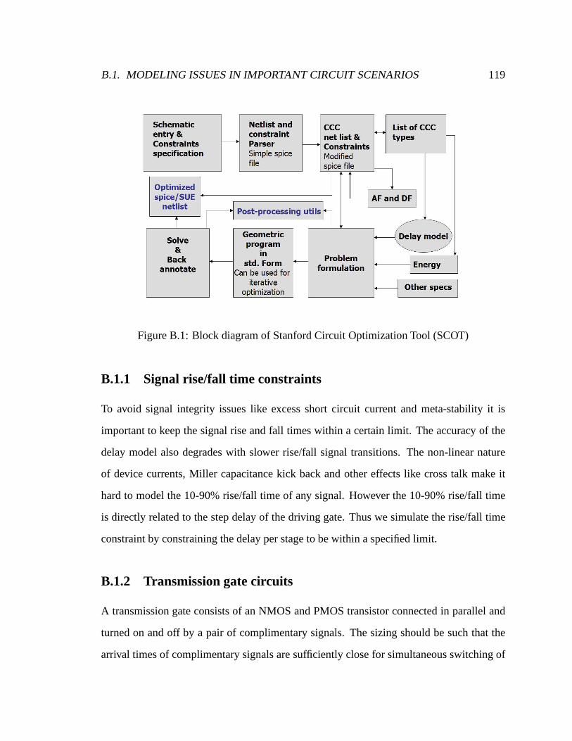
B.1. MODELING ISSUES IN IMPORTANT CIRCUIT SCENARIOS 119
Figure B.1: Block diagram of Stanford Circuit OptimizationTool (SCOT)
B.1.1 Signal rise/fall time constraints
To avoid signal integrity issues like excess short circuit current and meta-stability it is
important to keep the signal rise and fall times within a certain limit. The accuracy of the
delay model also degrades with slower rise/fall signal transitions. The non-linear nature
of device currents, Miller capacitance kick back and other effects like cross talk make it
hard to model the 10-90% rise/fall time of any signal. However the 10-90% rise/fall time
is directly related to the step delay of the driving gate. Thus we simulate the rise/fall time
constraint by constraining the delay per stage to be within aspecified limit.
B.1.2 Transmission gate circuits
A transmission gate consists of an NMOS and PMOS transistor connected in parallel and
turned on and off by a pair of complimentary signals. The sizing should be such that the
arrival times of complimentary signals are sufficiently close for simultaneous switching of

120 APPENDIX B. STANFORD CIRCUIT OPTIMIZATION TOOL
both devices. The improvement in the drive strength due to having two parallel transistors
of opposite kinds has to be modeled accurately for proper sizing of CCCs that contain a
transmission gate. While constraining the complimentary signals to arrive within a certain
time window is a non-convex constraint, what we care for is correct sizing that will enable
it. We model the arrival time of both the inputs of the transmission gate as the maximum
of their actual individual arrival times. This way the circuit generating the complimentary
signal is forced to speed paths leading to both the inputs, making them as close to each
other as possible. Examination of optimized circuits showsthat indeed this technique is
successful. With the assurance of almost simultaneous switching, we model the delay of
the transmission gate by using the same drive current expression as that of a CMOS gate,
with a higher effective width of the switching transistor. In our work, the width NMOS and
PMOS devices in a transmission gate is kept the same.
B.1.3 Local feedback - keepers
Figure B.2 shows two examples where local feedback is used inthe form of keepers in
dynamic logic and feedback inverters in latches. It is necessary to recognize the transistors
in the local feedback paths while sizing. First, their effect on forward signal propagation
due to parasitic capacitive loading and current fighting (ifany) should be considered. The
feedback devices have to be large enough to maintain the value the node against leakage,
and small enough to not prevent the node transition due to current fighting. SCOT allows
these two sided constraints to be included easily within theCCC itself. Having ensured
the transition, the increase in delay due to current fightingcan be taken into account by
assuming a higher effective load capacitance at that node. For sizing purposes, this works
well and enables the sizing of keepers and feedback inverters. Secondly, the delay through
the feedback path is not a part of the signal propagation delay through the circuit. In

B.1. MODELING ISSUES IN IMPORTANT CIRCUIT SCENARIOS 121
^*localcnst: WN /6 < WPK;
�^*localcnst: WPK < 0.3 WN;
WPK
WN
Vdd
gnd
clk
clk
out
in1
in2
inK
(a) dynamic 2 input nand gate
clk
clkclk b
clk b
gnd
Vdd
inK
data Q
(b) simple hold latch
Figure B.2: Local feedback in logic circuits: keepers and feedback inverters
SCOT, users can specify the inputs to feedback devices by naming them in a special way.
The optimizer then ignores the timing arcs that go through them. This also means ignoring
the timing arcs of any logic that feeds the keeper device alone. These circuits are then sized
based on other constraints like the signal rise/fall constraints and so on. To size self-reset
logic gates, additional pulse width constraints have to included for every gate to ensure a
good timing margin for reset.
B.1.4 Pulse width constraints
Certain circuits like pulse-mode flip-flops are designed to have a fixed pulse width between
two particular nets. This is usually done with an inverter chain. Figure B.3 shows a cartoon
where the problem is to optimize the entire combinational circuit CL for energy-efficiency
while designing sub-circuit S to have a fixed timing pulseTpulse between two nets n1 and n2.
The delay of sub-circuit S,Tckt, assuming n1 as the input would be a posynomial. Ideally
we would like to have a constraint such asTckt = Tpulse. However, equality involving a
posynomial is not allowed in GP. We can try to implement this constraint by specifying the
inequalitiesTckt ≤ Tpulse andTckt ≥ Tpulse. While the former is acceptable, the latter is

122 APPENDIX B. STANFORD CIRCUIT OPTIMIZATION TOOL
S
CL
n2n1inputs outputs
Tckt
Tpulse
Figure B.3: Combinational logic block CL with pulse width constraints on a sub-block S
still not a valid GP constraint1. A possible work around is to add the following constraints
instead.
Tckt ≤ Tpulse, Tn1 + max(Tpulse, Tckt) ≤ Tn2.
Here,Tn1 andTn2 are the signal arrival times at nets n1 and n2. The first constraint forces
the pulse to be no wider thanTpulse, while the second provides room for slowing S to the
point whereTckt = Tpulse. Unless the minimum size or slope constraint becomes active,
this is usually achieved in practice because downsizing S toachieveTpulse saves energy that
can be distributed to other parts of the circuit.
B.1.5 Modeling dual-rail gate delay
Dual rail domino gates like the one shown in Figure B.4 have complimentary input-pairs
that the gate delay modeling algorithm may mistake for independent inputs. This will result
in modeling the delay for the path that contains both the input and its complement. This
is clearly incorrect as such a path can never be sensitized. To avoid this in SCOT, the user
can specify a pair of inputs as complimentary inputs in the schematics so that the delay
1as it does not represent a convex space in the log-log domain.
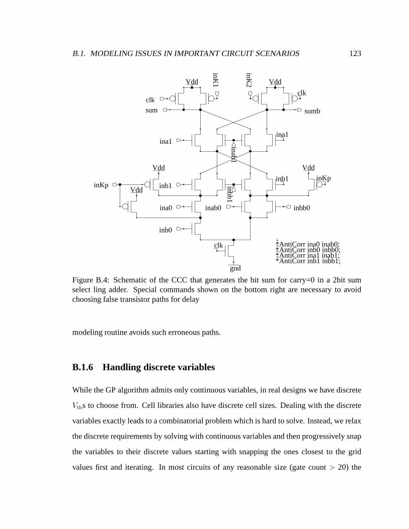
B.1. MODELING ISSUES IN IMPORTANT CIRCUIT SCENARIOS 123
Vdd
VddVdd
VddVdd
gnd
clk
clkclk
*AntiCorr ina0 inab0;
*AntiCorr ina1 inab1;*AntiCorr inb0 inbb0;
*AntiCorr inb1 inbb1;
ina0 inab0
ina1ina1 inab1
inb0
inbb0
inb1inb1
inbb1
sum sumb
inKpinKp
inK1
inK2
Figure B.4: Schematic of the CCC that generates the bit sum for carry=0 in a 2bit sumselect ling adder. Special commands shown on the bottom right are necessary to avoidchoosing false transistor paths for delay
modeling routine avoids such erroneous paths.
B.1.6 Handling discrete variables
While the GP algorithm admits only continuous variables, inreal designs we have discrete
Vths to choose from. Cell libraries also have discrete cell sizes. Dealing with the discrete
variables exactly leads to a combinatorial problem which ishard to solve. Instead, we relax
the discrete requirements by solving with continuous variables and then progressively snap
the variables to their discrete values starting with snapping the ones closest to the grid
values first and iterating. In most circuits of any reasonable size (gate count> 20) the

124 APPENDIX B. STANFORD CIRCUIT OPTIMIZATION TOOL
sensitivity of delay to individual device sizes orVths is very small. We observed less than
6 8 10 12 14 16 18 200.5
1
1.5
2
2.5
3
3.5
4
4.5
fixedVdd,Vth
variableVdd, Vth
Vth snapped to grid
delay in FO4
ener
gy
inp
J
Figure B.5: Snapping of discrete variables causes sub-optimality
1% degradation in 32-bit adder designs from using discreteVths. However, snapping does
lead to visible sub-optimality under some conditions. Figure B.5 shows the energy-delay
tradeoff curves for two optimizations on a 32bit adder, one in whichVdd andVth are fixed
to nominal values and the other in which they are variable with three discreteVths. Each
device has its ownVth. Naturally the latter results in a better tradeoff, as it hasmore
variables to design with. However, near the energy-delay points where the nominal values
of Vdd andVth are already very close to the optimal, designing with variable Vdd andVth
and then snapping can lead to a worse design. However the effect is negligible.

Bibliography
[1] M. Hershenson, S. Boyd, and T. Lee. Design of Pipeline Analog-to-Digital Convert-
ers via Geometric Programming. InProceedings of the IEEE/ACM International
Conference on Computer Aided Design, pages 317–324, November 2002.
[2] S. Augsburger and B. Nikolic. Combining dual-supply, dual-threshold and transistor
sizing for power reduction. InProceedings of the IEEE International Conference on
Computer Design: VLSI in Computers and Processors, pages 316–321, September
2002.
[3] O. Azizi, J. Collins, D. Patil, H. Wang, and M. Horowitz. Processor performance
modeling using symbolic simulation. To be presented atThe IEEE International
Conference on Computer Design: VLSI in Computers and Processors, April 2008.
[4] D. Bertsimas, K. Natarajan, and C.-P. Teo. Probabilistic combinatorial optimiza-
tion: Moments, semidefinite programming and asymptotic bounds. SIAM Journal
on Optimization, 15(1):185–209, 2005.
[5] S. Borkar, T. Karnik, S. Narendra, J. Tschanz, A. Keshavarzi, and V. De. Parameter
variations and impact on circuits and microarchitecture. In Proceedings of the40th
IEEE/ACM Design Automation Conference, pages 338–342, June 2003.
125

126 BIBLIOGRAPHY
[6] S. Boyd and S.-J. Kim. Geometric Programming for circuitoptimization. InPro-
ceedings of International Symposium on Physical Design (ISPD), pages 44–46,
April 2005.
[7] S. Boyd, S.-J. Kim, D. Patil, and M. Horowitz. Digital circuit sizing via geometric
programming.Operations Research, 53(6):899–932, 2005.
[8] S. Boyd, S.-J. Kim, D. Patil, and M. Horowitz. A heuristicmethod for statistical
digital circuit sizing. InProceedings of SPIE, volume 6156, 2006.
[9] S. Boyd, S.-J. Kim, L. Vandenberghe, and A. Hassibi. A tutorial on Geometric
Programming.Optimization and Engineering, 8(1):67–127, 2007.
[10] S. Boyd and L. Vandenberghe.Convex Optimization. Cambridge University Press,
2004.
[11] S. Boyd, L. Vandenberghe, A. El Gamal, and S. Yun. Designof robust global power
and ground networks. InProceedings ACM/SIGDA Symposium on Physical Design
(ISPD), pages 60–65, April 2001.
[12] R. E. Bryant. A switch-level model and simulator for MOSdigital systems.Trans-
action on Computers, C-33:160–177, Feb 1984.
[13] J. Burt and M. Garman. Conditional Monte Carlo: A simulation technique for
stochastic network analysis.Management Science, 18(1):207–217, September 1971.
[14] N. Chabini, I. Chabini, E. Aboulhamid, and Y. Savaria. Methods for minimizing
dynamic power consumption in synchronous designs with multiple supply voltages.
IEEE Transactions on Computer-Aided Design of Integrated Circuits and Systems,
22(3):346–351, 2003.
BIBLIOGRAPHY 127
[15] K. Chen, H. Hu, P. Fang, M. Lin, and D. Wollesen. Predicting CMOS speed with
gate oxide and voltage scaling and interconnect loading effects. IEEE Transactions
on Electron Devices, 44(11):1951–1957, 1997.
[16] T. Chen and S. Naffziger. Comparison of Adaptive Body Bias (ABB) and Adap-
tive Supply Voltage (ASV) for improving delay and leakage under the presence of
process variation.IEEE Transactions on VLSI systems, 11(5):888–899, Oct 2003.
[17] A. Conn, I. Elfadel, W. Molzen Jr., P. O’Brien, P. Strenski, C. Visweswariah, and
C. Whan. Gradient-based optimization of custom circuits using a static-timing for-
mulation. InProceedings of the36th IEEE/ACM Design Automation Conference,
pages 452–459, June 1999.
[18] D. Patil and S.-J. Kim. The Stanford Circuit Optimization Tool (SCOT) User
Guide, 2006. Available fromhttp://www.stanford.edu/class/ee371/
tools/SCOT_UserGuide.pdf .
[19] R. H. Dennard, F. H. Gaensslen, H. N. Yu, V. L. Rideout, E.Bassous, and A. R.
LeBlanc. Design of ion-implanted mosfets with very small physical dimensions.
IEEE journal of solid state circuits (JSSC), 9(5):256–268, Oct 1974.
[20] L. Devroye. Inequalities for the completion times of stochastic PERT networks.
Mathematics of Operations Research, 4(4):441–447, 1979.
[21] A. Dharchoudhury and S. M. Kang. Analytical fast timingsimulation of MOS cir-
cuits driving RC interconnects. InProceedings of10th International Conference on
VLSI design, pages 111–116, Jan 1997.
[22] B. Dodin. Bounding the project completion time distribution in PERT networks.
Operations Research, 33:862–881, 1985.

128 BIBLIOGRAPHY
[23] W. Elmore. The transient response of damped linear networks with particular regard
to wideband amplifiers.Journal of Applied Physics, 19(1):55–63, 1948.
[24] J. Fishburn and A. Dunlop. TILOS: A posynomial programming approach to tran-
sistor sizing. InDigest of Technical Papers of IEEE International Conference on
Computer-Aided Design (ICCAD), pages 326–328, 1985.
[25] P. Glasserman.Monte Carlo Methods in Financial Engineeting. Springer-Verlag,
2003.
[26] J. Hagstrom and N. Jane. Computing the probability distribution of project duration
in a PERT network.Networks, 20:231–244, 1990.
[27] M. C. Hansen, H. Yalcin, and J. P. Hayes. Unveiling the ISCAS-85 benchmarks: A
case study in reverse engineering.IEEE Design & Test of Computers, 16(3):72–80,
1999.
[28] D. Harris. A taxonomy of parallel prefix networks. InRecord of the Thirty-
Seventh Asilomar Conference on Signals, Systems and Computers, pages 2213–
2217, November 2003.
[29] D. Harris. Logical effort of higher valency adders. InRecord of the Thirty-
Eighth Asilomar Conference on Signals, Systems and Computers, pages 1358–1362,
November 2004.
[30] D. Harris and I. Sutherland. Logical effort of carry propagate adders. InProceeding
of the the Thrity-Seventh Asilomar Conference on Signals, Systems & Computers,
pages 873–878, 2003.
BIBLIOGRAPHY 129
[31] M. Hashimoto and H. Onodera. A performance optimization method by gate sizing
using statistical static timing analysis. InProceedings of the International Sympo-
sium on Physical Design (ISPD), pages 111–116, may 2000.
[32] U. Heller. On the shortest overall duration in stochastic acyclic network.Methods
of Operations Research, 42:85–104, 1981.
[33] M. Hershenson, S. Boyd, and T. Lee. Optimal design of a CMOS op-amp via geo-
metric programming.IEEE Transactions on Computer-Aided Design of Integrated
Circuits and Systems, 20(1):1–21, January 2001.
[34] M. A. Horowitz. Timing models for MOS circuits. PhD thesis, Stanford University,
1984.
[35] M. A. Horowitz. Lecture notes of ee313, Digital MOS integrated circuits, 2000.
Available fromhttp://eeclass.stanford.edu/ee313/ .
[36] W. Hung, Y. Xie, N. Vijaykrishnan, M. Kandemir, M. Irwin, and Y. Tsai. Total
power optimization through simultaneously multiple-VDD multiple-VTH assignment
and device sizing with stack forcing. InProceedings of International Symposium on
Low Power Electronics and Design (ISLPED), pages 144–149, August 2004.
[37] F. Ishihara, F. Sheikh, and B. Nikolic. Level conversion for dual-supply systems.
IEEE Transactions on Very Large Scale Integration (VLSI) Systems, 12(2):185–195,
2004.
[38] E. T. A. F. Jacobs and M. R. C. M. Berkelaar. Gate sizing using a statistical delay
model. InProceedings of Design and Test in Europe (DATE) Conference.
130 BIBLIOGRAPHY
[39] M. Johnson, D. Somasekhar, L.-Y. Chiou, and K. Roy. Leakage control with efficient
use of transistor stacks in single threshold CMOS.IEEE Transactions on Very Large
Scale Integration (VLSI) Systems, 10(1):1–5, February 2002.
[40] S. Joshi and S. Boyd. An efficient method for large-scalegate sizing. To appear in
IEEE Transactions on Circuits and Systems, Submitted in December 2006.
[41] S. Joshi, S. Boyd, and R. W. Dutton. Optimal doping profiles via Geometric Pro-
gramming.IEEE Transactions on Electron devices, 52(12):2660–2675, Dec 2005.
[42] K. Kasamsetty, M. Ketkar, and S. Sapatnekar. A new classof convex functions for
delay modeling and its application to the transistor sizingproblem. IEEE Transac-
tions on Computer-Aided Design of Integrated Circuits and Systems, 19(7):779–788,
July 2000.
[43] J. F. Kenney and E. S. Keeping.Mathematics of Statistics, Part 2. Van Nostrand,
second edition.
[44] M. Ketkar and S. Sapatnekar. Standby power optimization via transistor sizing and
dual threshold voltage assignment. InProceedings of the IEEE/ACM international
Conference on Computer-Aided Design, pages 375–378, November 2002.
[45] S.-J. Kim, S. Boyd, S. Yun, D. Patil, and M. Horowitz. A heuristic for op-
timizing stochastic activity networks with applications to statistical digital cir-
cuit sizing. Optimization and Engineering, 8(4):397–430, 2007. Available from
www.stanford.edu/ ˜ boyd/heur_san_opt.html .
[46] S. Knowles. A family of adders. InProceedings of14th IEEE Symposium on Com-
puter Arithmetic, pages 30–34, 1999.

BIBLIOGRAPHY 131
[47] P. Kongetira, K. Aingaran, and K. Olukotun. Niagara: a 32-way multithreaded Sparc
processor.IEEE Micro, 25:21–29, Mar-Apr 2005.
[48] S. Kulkarni and D. Sylvester. High performance level conversion for dualVDD de-
sign.IEEE Transactions on Very Large Scale Integration (VLSI) Systems, 12(9):926–
936, 2004.
[49] R. E. Ladner and M. J. Fischer. Parallel prefix computation. Journal of ACM,
27(4):831–838, Oct 1980.
[50] A. S. Leon, K. W. Tam, J. L. Shin, D. Weisner, and F. Schumacher. A power-efficient
high-throughput 32-thread SPARC processor.IEEE Journal of Solid-State Circuits,
42:7–16, 2007.
[51] H. Ling. High speed binary adder.IBM Journal of Research and Development,
25(3):126–130, May 1981.
[52] A. Ludwig, R. Mohring, and F. Stork. A computational study on bounding the
makespan distribution in stochastic project networks.Annals of Operations Re-
search, 102:49–64, 2001.
[53] M. Mani, A. K. Singh, and M. Orshansky. Joint design-time and post-silicon mini-
mization of parametric yield loss using adjustable robust optimization. In(ICCAD)
IEEE/ACM International Conference on Computer-Aided design., pages 19–26, Nov
2006.
[54] D. Markovic, V. Stojanovic, B. Nikolic, M. Horowitz, and R. Brodersen. Methods
for true energy-performance optimization.IEEE Journal of Solid-State Circuits,
39(8):1282–1293, 2004.

132 BIBLIOGRAPHY
[55] S. Mathew, M. Anders, R. Krishnamurthy, and S. Borkar. A4GHz 130-nm address
generation unit with 32-bit sparse-tree adder core.IEEE Journal of Solid State Cir-
cuits, 38(5):689–695, 2003.
[56] S. K. Mathew, M. A. Anders, B. Bloechel, T. Nguyen, R. K. Krishnamurthy, and
S. Borkar. A 4-GHz 300-mW 64-bit integer execution ALU with dual supply volt-
ages in 90-nm CMOS.IEEE Journal of Solid-State Circuits, 40(1):44–51, Jan 2005.
[57] R. McGowen, C. A. Poirier, C. Bostak, J. Ignowski, M. Millican, W. H. Parks, and
S. Naffziger. Power and temperature control on a 90-nm Itanium family processor.
IEEE Journal of Solid-State Circuits, 41:229–237, 2006.
[58] I. Mejilson and A. Nadas. Convex majorization with an application to the length of
critical path.Journal of Applied Probability, 16:671–677, 1979.
[59] Micro Magic Inc. SUE Design Manager datasheet, 2004. Available fromhttp:
//www.micromagic.com/tools/sue_datasheet.html .
[60] G. Moore. Cramming more Components into Integrated Circuits. Electronics Mag-
azine, 38(8):256–268, April 1965.
[61] MOSEK ApS. The MOSEK Optimization Tools Version 3 User’s Manual and Ref-
erence, 2002. Available fromhttp://www.mosek.com .
[62] S. Naffziger. A sub-nanosecond0.5µm 64b adder design. InIEEE International
Solid-State Circuits Conference Digest of Technical Papers, pages 362–363, Febru-
ary 1996.
BIBLIOGRAPHY 133
[63] S. Narendra, V. De, S. Borkar, D. A. Antoniadis, and A. P.Chandrakasan. Full-chip
subthreshold leakage power prediction and reduction techniques for sub-0.18-µm
CMOS. IEEE Journal of Solid-State Circuits, 39(3):501–510, 2004.
[64] S. Nassif. Within chip variability analysis. InInternational Electron Devices Meet-
ing (IEDM) Technical Digest, pages 283–286, Dec 1998.
[65] T. N. Nguyen and J. D. Plummer. Physical mechanisms responsible for short-channel
effects in MOS devices. InInternational Electron Devices Meeting (IEDM) Techni-
cal digest, pages 596–599, 1981.
[66] E. J. Nowak. Maintaining the benefits of CMOS scaling when scaling bogs down.
IBM Journal of Research and Development, 46(2/3):169–180, May 2002.
[67] V. G. Oklobdzija, B. R. Zeydel, H. Q. Dao, S. Mathew, and R. Krishnamurthy. Com-
parison of high-performance VLSI adders in the energy-delay space.IEEE Trans-
actions on Very Large Scale Integration (VLSI) Systems, 13(6):754–758, june 2005.
[68] D. Patil, R. Ho, O. Azizi, R. Ananthraman, and M. Horowitz. Robust energy-
efficient adder topologies. InProceedings of18th IEEE Symposium on Computer
Arithmetic, pages 30–34, 2007.
[69] D. Patil, S. Yun, S.-J. Kim, S. Boyd, and M. Horowitz. A new method for design
of robust digital circuits. InProceedings of6th International Symposium on Quality
Electronic Design (ISQED), 2005.
[70] M. Pelgrom, C.-J. Duinmaijer, and A.-P.-G. Welbers. Matching properties of MOS
transistors.IEEE Journal of Solid State Circuits, 24(5):1433–1439, October 1989.

134 BIBLIOGRAPHY
[71] D. C. Pham, T. Aipperspach, D. Boerstler, M. Bolliger, R. Chaudhry, D. Cox, P. Har-
vey, P. M. Harvey, H. P. Hofstee, C. Johns, J. Kahle, A. Kameyama, J. Keaty, Y. Ma-
subuchi, M. Pham, J. Pille, S. Posluszny, M. Riley, D. L. Stasiak, M. Suzuoki,
O. Takahashi, J. Warnock, S. Weitzel, D. Wendel, and K. Yazawa. Overview of
the architecture, circuit design, and physical implementation of a first-generation
Cell processor.IEEE Journal of Solid-state circuits, 41:179–196, Jan 2006.
[72] R. F. Pierret.Semiconductor device fundamentals. Addison-Wesley, 1996.
[73] S. Raj, S. B. K. Vrudhula, and J. Wang. A methodology to improve timing yield
in the presence of process variations. InProceedings of the41st IEEE/ACM Design
Automation Conference (DAC), pages 448–453, San Diego, California, Jun 2004.
[74] P. Robillard and M. Trahan. The completion times of PERTnetworks.Operations
Research, 25:15–29, 1976.
[75] S. Rusu, S. Tam, H. Muljono, D. Ayers, and J. Chang. A dual-core multi-threaded
Xeon processor with 16MB L3 cache. InIEEE International Solid-State Circuits
Conference Digest of Technical Papers, pages 315–324, Feb 2006.
[76] T. Sakurai and A. Newton. Alpha-power law MOSFET model and its application
to CMOS inverter delay and other formulas.IEEE Journal of Solid-State Circuits,
25(2):584–593, 1990.
[77] V. Sandararajan and K. K. Parhi. Synthesis of low power CMOS VLSI circuits using
dual supply voltages. InProceedings of35th Design Automation Conference, June
1999.
[78] R. Serfling.Approximation Theorems of Mathematical Statistics. Wiley, New York,
1980.

BIBLIOGRAPHY 135
[79] A. Shogan. Bounding distributions for a stochastic PERT network.Networks, 7:359–
381, 1977.
[80] J. Sklansky. Conditional-sum addition logic.IRE Transactions on Electronic Com-
puters, EC-9:226–231, June 1960.
[81] R. Van Slyke. Monte Carlo methods and the PERT problem.Operations Research,
11:839–860, 1963.
[82] C. G. Sodini, P. K. Ko, and J. L. Moll. The effect of high fields on MOS device and
circuit performance.IEEE Transactions of Electron Devices, 31:1386–1393, Oct
1984.
[83] A. Srivastava and D. Sylvester. Minimizing total powerby simultaneousVdd/Vth
assignment.IEEE Transactions on Computer-Aided Design of Integrated Circuits
and Systems, 23(5):665–677, 2004.
[84] A. Srivastava, D. Sylvester, and D. Blaauw. Power minimization using simulata-
neous gate sizing dual-Vdd and dual-Vth assignment. InProceedings of the41st
Design Automation Conference, pages 783–787, jun 2004.
[85] L. Su, R. Schulz, J. Adkisson, K. Beyer, G. Biery, W. Cote, E. Crabbe, D. Edel-
stein, J. Ellis-Monaghan, E. Eld, D. Foster, R. Gehres, R. Goldblatt, N. Greco,
C. Guenther, J. Heidenreich, J. Herman, D. Kiesling, L. Lin,S. H. Lo, J. McKenna,
C. Megivern, H. Ng, J. Oberschmidt, A. Ray, N. Rohrer, K. Tallman, T. Wagner,
and B. Davari. A high-performance sub-0.25µm CMOS technology with multiple
thresholds and copper interconnects. InSymposium on VLSI Technology Digest of
Technical Papers, pages 18–19, June 1998.

136 BIBLIOGRAPHY
[86] R. Sullivan and J. Hayya. A comparison of the Method of Bounding Distributions
(MBD) and Monte Carlo simulation for analyzing stochastic acyclic networks.Op-
erations Research, 28(3):614–617, May-Jun. 1980.
[87] I. Sutherland, B. Sproull, and D. Harris.Logical Effort: Designing fast CMOS
Circuits. Morgan Kaufmann Publishers, San Francisco, CA, 1999.
[88] Y. Taur and T. H. Ning.Fundamentals of modern VLSI devices. Cambridge Univer-
sity Press, ninth edition, 2006.
[89] K.-Y. Toh, P.-K. Ko, and R. Meyer. An engineering model for short channel MOS
devices.IEEE Journal of Solid-State Circuits, 23(4):950–958, 1988.
[90] J. W. Tschanz, J. T. Kao, S. G. Narendra, R. Nair, D. A. Antoniadis, A. P. Chan-
drakasan, and V. De. Adaptive body bias for reducing impactsof die-to-die and
within-die parameter variations on microprocessor frequency and leakage.IEEE
Journal of Solid-State Circuits, 37(11):1396–1402, Nov 2002.
[91] N. Tzartzanis, W. W. Walker, H. Nguyen, and A. Inoue. A 34word×64b 10R/6W
write-through self timed dual-supply-voltage register file. In IEEE International
Solid-State Circuits Conference Digest of Technical Papers, pages 338–339, Feb
2002.
[92] K. Usami and M. Horowitz. Clustered voltage scaling technique for low-power
design. InProceedings of the 1995 International Symposium on Low Power Design,
pages 3–8, San Diego, CA, June 1995.
[93] A. van der Vaart.Asymptotics Statistics. Cambridge University Press, 1998.

BIBLIOGRAPHY 137
[94] Y. Wang and K. K. Parhi. A unified adder design. InRecord of the35th Asilomar
Conference on Signals, Systems and Computers, volume 1, pages 177–282, 2001.
[95] G. Weiss. Stochastic bounds on distributions of optimal value functions with applica-
tions to PERT, network flows and reliability.Operations Research, 34(4):595–605,
1986.
[96] N. Weste and D. Harris.CMOS VLSI Design: A Circuits and Systems Perspective.
Addison Wesley, third edition, 2004.
[97] L. S. Y. Wong, S. Hossain, A. Ta, J. Edvinsson, D. H. Rivas, and H. Naas. A very
low-power CMOS mixed-signal IC for implantable pacemaker applications. IEEE
Journal of Solid-State Circuits, 39:2446–2456, 2004.
[98] P. N. Strenski D. J. Hathaway X. Bai, C. Visweswariah. Uncertainty aware circuit
optimization. InProceedings of the39th IEEE/ACM Design Automation Conference
(DAC).
[99] Y.-J. Yeh, S.-Y. Kuo, and J.-Y. Jou. Converter-free multiple-voltage scaling tech-
niques for low-power CMOS digital design.IEEE Transactions on Computer-Aided
Design of Integrated Circuits and Systems, 20(1):172–176, 2001.
[100] R. Zlatanovici and B. Nikolic. Power-performance optimal 64-bit carry-lookahead
adders. InProceedings of the29th European Solid-State Circuits Conference (ESS-
CIRC), pages 321–324, 2003.