design, prototype, and manufacture of a circuit level ... · down to 5 volts in order to power the...
TRANSCRIPT
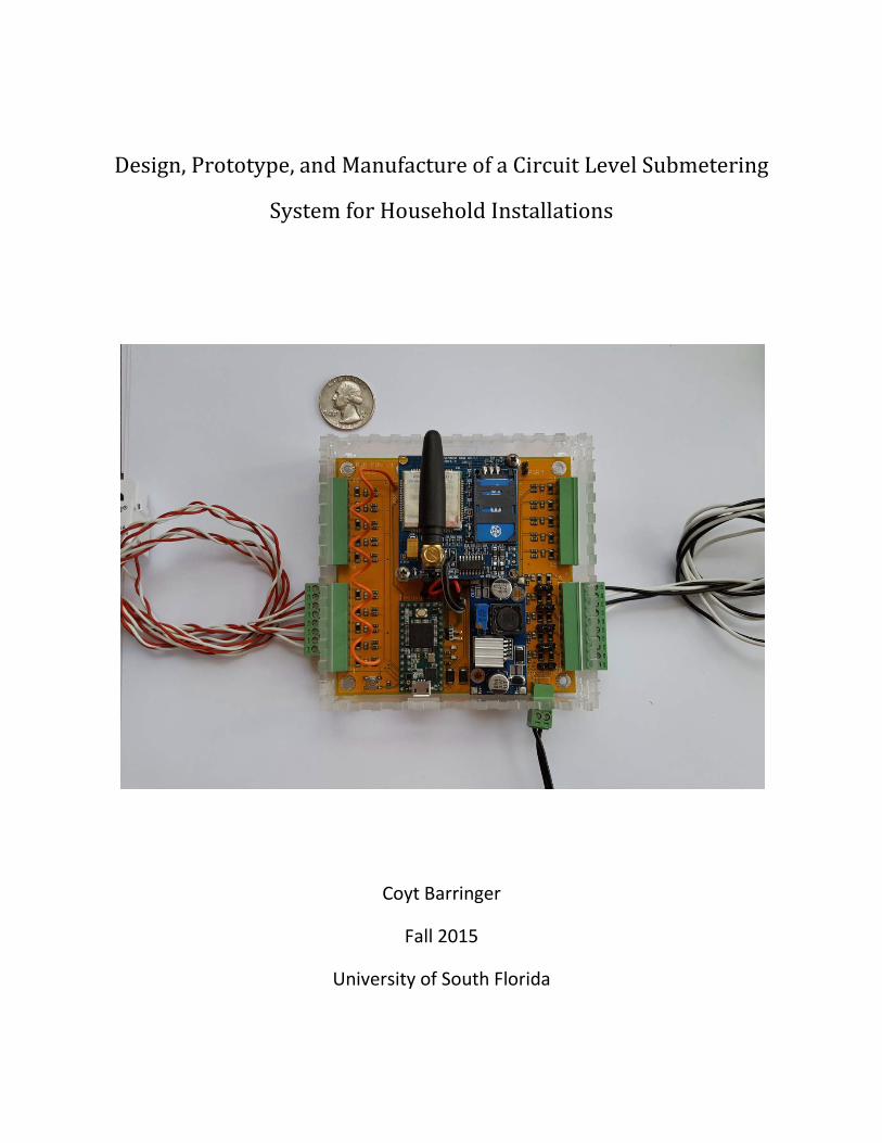
Design, Prototype, and Manufacture of a Circuit Level Submetering
System for Household Installations
Coyt Barringer
Fall 2015
University of South Florida

2
Introduction
Engineering and business often go hand in hand. The following project is a direct result
of this relationship. Over the summer of 2015 a startup business was formed with the intention
of designing, building, and selling a device to allow landlords of multi-tenant properties to
accurately record and bill tenants for their power usage. Further business details aside, several
constraints were placed on the product including its proposed functionality, size, ease of
installation, and price. The overall system would consist of two parts – a hardware component
installed in the property to be monitored, and a remote server for collecting, analyzing, and
displaying the recorded data. This technical report will detail the design, prototype, and
manufacture of the former, as this was the task of the author. The first half of the following
discussion is organized into a system overview followed by details of each subsystem. The
remainder will present the work performed in a semi-chronological order.
System Architecture and Constraints
Before hardware could be designed, an outline for the system was thought up based on
several constraints. It was decided that the power monitoring functionality would work by the
use of small clip on current transformers, or CTs, attached to every circuit in the house. In this
way, current draw, and thus power, on each circuit can be measured. Alternatives to CT’s, such
as Hall Effect sensors, current shunts, and Rogowski coils were considered, but CT’s were
chosen due to cost and ease of use. These CTs would be installed on the wires immediately
leaving the circuit breakers in the standard household breaker box. The benefit of this method
lies in the isolating properties of CT’s. With clip on CT’s, no wire inside the breaker box needs to
be disconnected to install the current monitoring system. Furthermore, a wide range of
inexpensive CT’s are available which met the design requirements. The majority of household
circuit breakers are rated at 30A, so a CT with an upper limit of this value was chosen. Dechang
Electronics model SCT-006 30A split core current transformer was ultimately chosen because it
met a low price point of $2.50 per CT, had a very small size allowing several in a breaker box,
and met the electrical requirements [1]. Collecting current data to this CT will be discussed
later. 20 SCT-006 CT’s would be needed per metering system as this is an estimate of the
3
number of 30A breakers in the average household breaker box. Designs were also implemented
allowing up to five larger CT’s to be attached for monitoring of 240V appliances such as air
conditioning units, water heaters, stoves, etc…
Telemetry methods were carefully selected so the accumulated power data would not
be lost in transit to the internet connected server for display. Two separate internet
connections were implemented - the first and main method was the use of the new ESP8266 by
Espressif, a small microcontroller with built in Wi-Fi capability. This chip allows the power
monitoring system to connect to a household Wi-Fi network. The second method is via a GSM
cellular modem, specifically the SIMCOM SIM900 quad-band module. This module allows
TCP/IP data containing the power readings to be transmitted to the internet if Wi-Fi is not
available. Both of these devices were selected due to their low cost (~$5 for the ESP8266 and
~$20 for the SIM900) as well as their ease of use and thorough online documentation. As an
additional feature and the 3rd wireless device on the system, a small and inexpensive UHF data
radio/modem was added. This modem allows future sensor nodes to be designed and linked to
the power monitoring system creating a Home Area Network or HAN if you will.
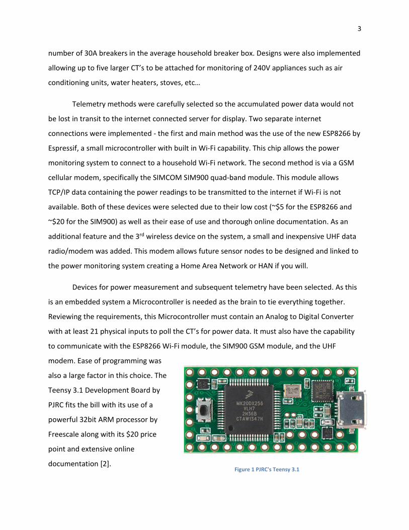
Devices for power measurement and subsequent telemetry have been selected. As this
is an embedded system a Microcontroller is needed as the brain to tie everything together.
Reviewing the requirements, this Microcontroller must contain an Analog to Digital Converter
with at least 21 physical inputs to poll the CT’s for power data. It must also have the capability
to communicate with the ESP8266 Wi-Fi module, the SIM900 GSM module, and the UHF
modem. Ease of programming was
also a large factor in this choice. The
Teensy 3.1 Development Board by
PJRC fits the bill with its use of a
powerful 32bit ARM processor by
Freescale along with its $20 price
point and extensive online
documentation [2]. Figure 1 PJRC's Teensy 3.1
4
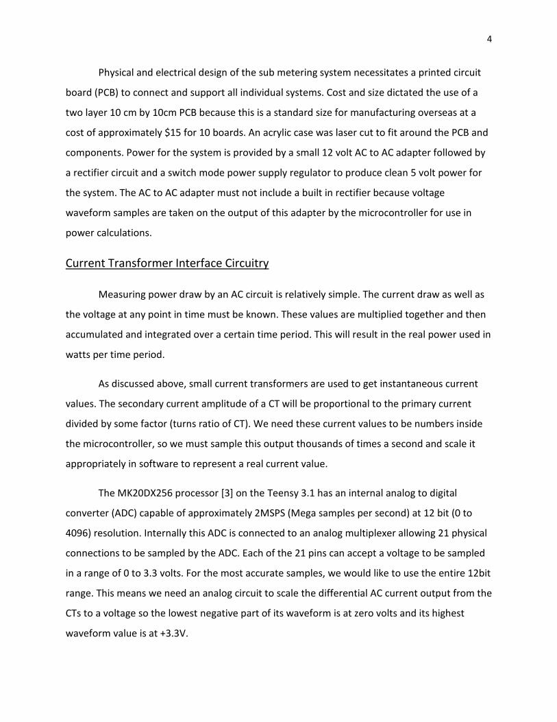
Physical and electrical design of the sub metering system necessitates a printed circuit
board (PCB) to connect and support all individual systems. Cost and size dictated the use of a
two layer 10 cm by 10cm PCB because this is a standard size for manufacturing overseas at a
cost of approximately $15 for 10 boards. An acrylic case was laser cut to fit around the PCB and
components. Power for the system is provided by a small 12 volt AC to AC adapter followed by
a rectifier circuit and a switch mode power supply regulator to produce clean 5 volt power for
the system. The AC to AC adapter must not include a built in rectifier because voltage
waveform samples are taken on the output of this adapter by the microcontroller for use in
power calculations.
Current Transformer Interface Circuitry
Measuring power draw by an AC circuit is relatively simple. The current draw as well as
the voltage at any point in time must be known. These values are multiplied together and then
accumulated and integrated over a certain time period. This will result in the real power used in
watts per time period.
As discussed above, small current transformers are used to get instantaneous current
values. The secondary current amplitude of a CT will be proportional to the primary current
divided by some factor (turns ratio of CT). We need these current values to be numbers inside
the microcontroller, so we must sample this output thousands of times a second and scale it
appropriately in software to represent a real current value.
The MK20DX256 processor [3] on the Teensy 3.1 has an internal analog to digital
converter (ADC) capable of approximately 2MSPS (Mega samples per second) at 12 bit (0 to
4096) resolution. Internally this ADC is connected to an analog multiplexer allowing 21 physical
connections to be sampled by the ADC. Each of the 21 pins can accept a voltage to be sampled
in a range of 0 to 3.3 volts. For the most accurate samples, we would like to use the entire 12bit
range. This means we need an analog circuit to scale the differential AC current output from the
CTs to a voltage so the lowest negative part of its waveform is at zero volts and its highest
waveform value is at +3.3V.
5
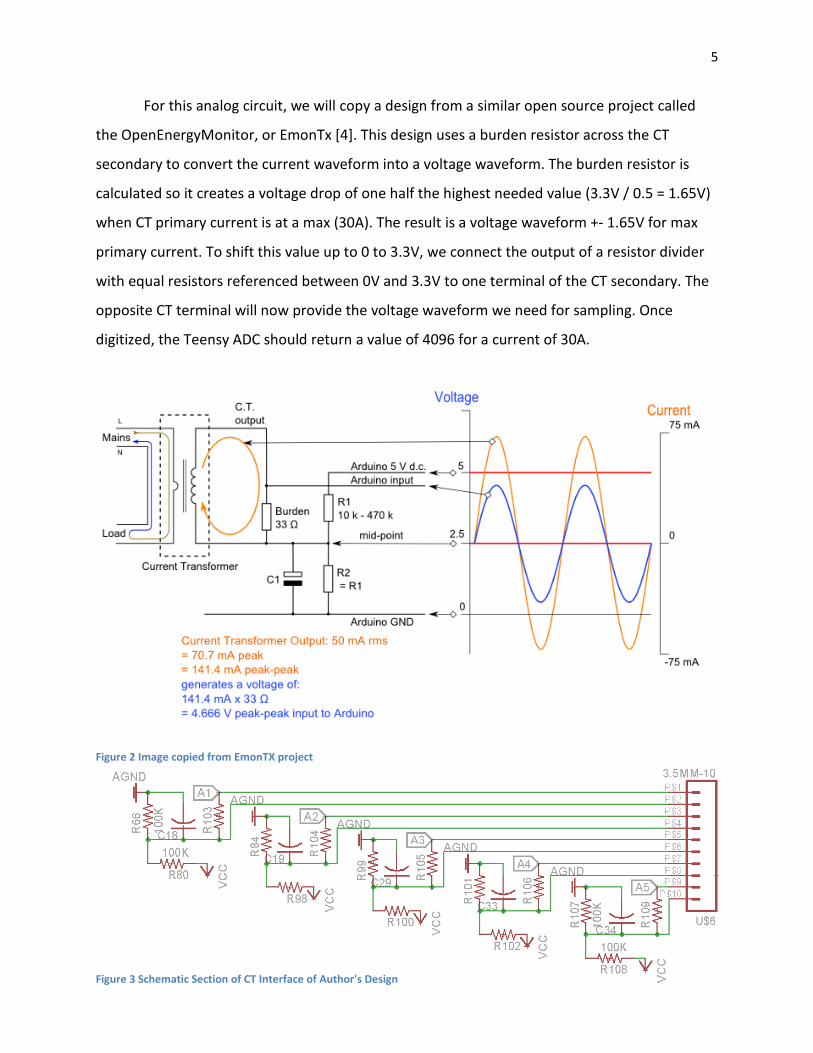
For this analog circuit, we will copy a design from a similar open source project called
the OpenEnergyMonitor, or EmonTx [4]. This design uses a burden resistor across the CT
secondary to convert the current waveform into a voltage waveform. The burden resistor is
calculated so it creates a voltage drop of one half the highest needed value (3.3V / 0.5 = 1.65V)
when CT primary current is at a max (30A). The result is a voltage waveform +- 1.65V for max
primary current. To shift this value up to 0 to 3.3V, we connect the output of a resistor divider
with equal resistors referenced between 0V and 3.3V to one terminal of the CT secondary. The
opposite CT terminal will now provide the voltage waveform we need for sampling. Once
digitized, the Teensy ADC should return a value of 4096 for a current of 30A.
Figure 2 Image copied from EmonTX project
Figure 3 Schematic Section of CT Interface of Author's Design

6
With this analog circuit design, component values were calculated to interface the 30A
SCT-006 YHDC CT’s as well as 80A SCT-010 YHDC CT’s for 240V appliance measurements.
For SCT-006: 30A:37.5mA or 1:800 turns ratio
𝑆𝑆𝑆𝑆𝑆𝑆𝑆𝑆𝑆𝑆𝑆𝑆𝑆𝑆𝑆𝑆𝑆𝑆 𝑃𝑃𝑆𝑆𝑆𝑆𝑃𝑃 𝐶𝐶𝐶𝐶𝑆𝑆𝑆𝑆𝑆𝑆𝑆𝑆𝐶𝐶 = 30𝐴𝐴𝑟𝑟𝑟𝑟𝑟𝑟∗ √2800
= 53𝑚𝑚𝑚𝑚
𝐼𝐼𝑆𝑆𝑆𝑆𝑆𝑆𝐼𝐼 𝐵𝐵𝐶𝐶𝑆𝑆𝑆𝑆𝑆𝑆𝑆𝑆: (3.3𝑉𝑉÷ 2)53𝑚𝑚𝐴𝐴
= 31.132 𝑂𝑂ℎ𝑚𝑚𝑚𝑚
𝑃𝑃𝑆𝑆𝑆𝑆𝑃𝑃 𝑃𝑃𝑆𝑆𝑃𝑃𝑆𝑆𝑆𝑆 𝐷𝐷𝐷𝐷𝑚𝑚𝑚𝑚𝐷𝐷𝐷𝐷𝑆𝑆𝐶𝐶𝐷𝐷𝑆𝑆𝑆𝑆: 53𝑚𝑚𝑚𝑚 ∗ 3.3𝑉𝑉 = 0.1748 𝑊𝑊𝑆𝑆𝐶𝐶𝐶𝐶𝑚𝑚
31 Ohm +- 1% 0.25W Burden Resistor was chosen
For SCT-010: 1:3000 turns ratio
𝑆𝑆𝑆𝑆𝑆𝑆𝑆𝑆𝑆𝑆𝑆𝑆𝑆𝑆𝑆𝑆𝑆𝑆 𝑃𝑃𝑆𝑆𝑆𝑆𝑃𝑃 𝐶𝐶𝐶𝐶𝑆𝑆𝑆𝑆𝑆𝑆𝑆𝑆𝐶𝐶 = 80𝐴𝐴𝑟𝑟𝑟𝑟𝑟𝑟∗ √23000
= 37.7𝑚𝑚𝑚𝑚
𝐼𝐼𝑆𝑆𝑆𝑆𝑆𝑆𝐼𝐼 𝐵𝐵𝐶𝐶𝑆𝑆𝑆𝑆𝑆𝑆𝑆𝑆: (3.3𝑉𝑉÷ 2)37.7𝑚𝑚𝐴𝐴
= 43.75 𝑂𝑂ℎ𝑚𝑚𝑚𝑚
𝑃𝑃𝑆𝑆𝑆𝑆𝑃𝑃 𝑃𝑃𝑆𝑆𝑃𝑃𝑆𝑆𝑆𝑆 𝐷𝐷𝐷𝐷𝑚𝑚𝑚𝑚𝐷𝐷𝐷𝐷𝑆𝑆𝐶𝐶𝐷𝐷𝑆𝑆𝑆𝑆: 37.7𝑚𝑚𝑚𝑚 ∗ 3.3𝑉𝑉 = 0.1244 𝑊𝑊𝑆𝑆𝐶𝐶𝐶𝐶𝑚𝑚
44 Ohm +- 1% 0.25W Burden Resistor was chosen
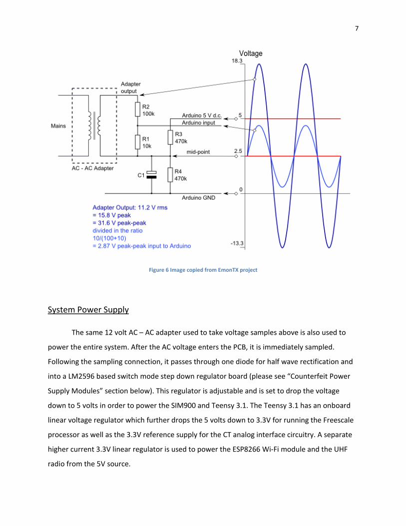
Voltage Transformer Interface Circuitry
Circuitry used to interface with and sample the household voltage waveform is nearly
identical to the circuitry used to scale the CTs discussed above. Again, a great diagram showing
this method taken from the EmonTX project is below [4]. Ultimately, a 174KOhm resistor and a
10KOhm resistor were used for the main divider.
Figure 4 SCT-006 CT
Figure 5 STC-010 CT
7
Figure 6 Image copied from EmonTX project
System Power Supply
The same 12 volt AC – AC adapter used to take voltage samples above is also used to
power the entire system. After the AC voltage enters the PCB, it is immediately sampled.
Following the sampling connection, it passes through one diode for half wave rectification and
into a LM2596 based switch mode step down regulator board (please see “Counterfeit Power
Supply Modules” section below). This regulator is adjustable and is set to drop the voltage
down to 5 volts in order to power the SIM900 and Teensy 3.1. The Teensy 3.1 has an onboard
linear voltage regulator which further drops the 5 volts down to 3.3V for running the Freescale
processor as well as the 3.3V reference supply for the CT analog interface circuitry. A separate
higher current 3.3V linear regulator is used to power the ESP8266 Wi-Fi module and the UHF
radio from the 5V source.
8
All power on the system comes from either a 5V USB connection built into the Teensy
3.1 or from the 5V Switch Mode Regulator. These two sources are isolated from each other by
use of diodes so either source can power the board, but power will not be able to flow
backwards into the USB connection as this could damage a computer.
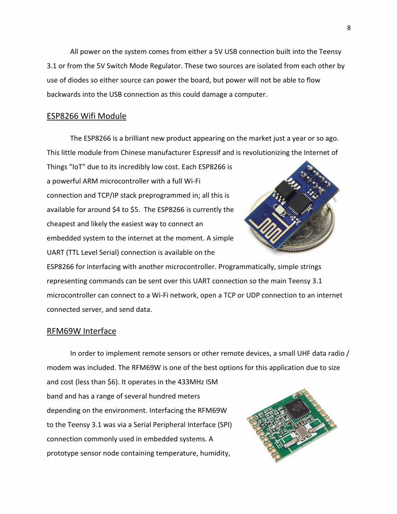
ESP8266 Wifi Module
The ESP8266 is a brilliant new product appearing on the market just a year or so ago.
This little module from Chinese manufacturer Espressif and is revolutionizing the Internet of
Things “IoT” due to its incredibly low cost. Each ESP8266 is
a powerful ARM microcontroller with a full Wi-Fi
connection and TCP/IP stack preprogrammed in; all this is
available for around $4 to $5. The ESP8266 is currently the
cheapest and likely the easiest way to connect an
embedded system to the internet at the moment. A simple
UART (TTL Level Serial) connection is available on the
ESP8266 for interfacing with another microcontroller. Programmatically, simple strings
representing commands can be sent over this UART connection so the main Teensy 3.1
microcontroller can connect to a Wi-Fi network, open a TCP or UDP connection to an internet
connected server, and send data.
RFM69W Interface
In order to implement remote sensors or other remote devices, a small UHF data radio /
modem was included. The RFM69W is one of the best options for this application due to size
and cost (less than $6). It operates in the 433MHz ISM
band and has a range of several hundred meters
depending on the environment. Interfacing the RFM69W
to the Teensy 3.1 was via a Serial Peripheral Interface (SPI)
connection commonly used in embedded systems. A
prototype sensor node containing temperature, humidity,
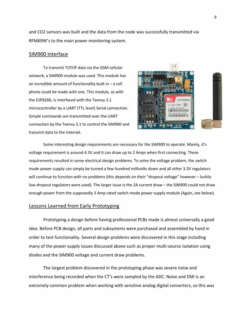
9
and CO2 sensors was built and the data from the node was successfully transmitted via
RFM69W’s to the main power monitoring system.
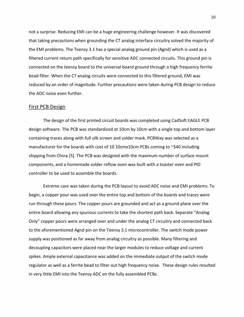
SIM900 Interface
To transmit TCP/IP data via the GSM cellular
network, a SIM900 module was used. This module has
an incredible amount of functionality built in – a cell
phone could be made with one. This module, as with
the ESP8266, is interfaced with the Teensy 3.1
microcontroller by a UART (TTL level) Serial connection.
Simple commands are transmitted over the UART
connection by the Teensy 3.1 to control the SIM900 and
transmit data to the internet.
Some interesting design requirements are necessary for the SIM900 to operate. Mainly, it’s
voltage requirement is around 4.3V and It can draw up to 2 Amps when first connecting. These
requirements resulted in some electrical design problems. To solve the voltage problem, the switch
mode power supply can simply be turned a few hundred millivolts down and all other 3.3V regulators
will continue to function with no problems (this depends on their “dropout voltage” however – luckily
low dropout regulators were used). The larger issue is the 2A current draw – the SIM900 could not draw
enough power from the supposedly 3 Amp rated switch mode power supply module (Again, see below).
Lessons Learned from Early Prototyping
Prototyping a design before having professional PCBs made is almost universally a good
idea. Before PCB design, all parts and subsystems were purchased and assembled by hand in
order to test functionality. Several design problems were discovered in this stage including
many of the power supply issues discussed above such as proper multi-source isolation using
diodes and the SIM900 voltage and current draw problems.
The largest problem discovered in the prototyping phase was severe noise and
interference being recorded when the CT’s were sampled by the ADC. Noise and EMI is an
extremely common problem when working with sensitive analog digital converters, so this was
10
not a surprise. Reducing EMI can be a huge engineering challenge however. It was discovered
that taking precautions when grounding the CT analog interface circuitry solved the majority of
the EMI problems. The Teensy 3.1 has a special analog ground pin (Agnd) which is used as a
filtered current return path specifically for sensitive ADC connected circuits. This ground pin is
connected on the teensy board to the universal board ground through a high frequency ferrite
bead filter. When the CT analog circuits were connected to this filtered ground, EMI was
reduced by an order of magnitude. Further precautions were taken during PCB design to reduce
the ADC noise even further.
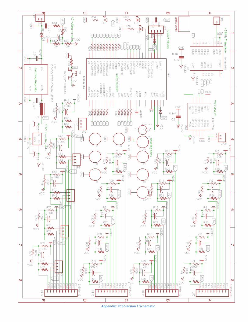
First PCB Design
The design of the first printed circuit boards was completed using CadSoft EAGLE PCB
design software. The PCB was standardized at 10cm by 10cm with a single top and bottom layer
containing traces along with full silk screen and solder mask. PCBWay was selected as a
manufacturer for the boards with cost of 10 10cmx10cm PCBs coming to ~$40 including
shipping from China [5]. The PCB was designed with the maximum number of surface mount
components, and a homemade solder reflow oven was built with a toaster oven and PID
controller to be used to assemble the boards.
Extreme care was taken during the PCB layout to avoid ADC noise and EMI problems. To
begin, a copper pour was used over the entire top and bottom of the boards and traces were
run through these pours. The copper pours are grounded and act as a ground plane over the
entire board allowing any spurious currents to take the shortest path back. Separate “Analog
Only” copper pours were arranged over and under the analog CT circuitry and connected back
to the aforementioned Agnd pin on the Teensy 3.1 microcontroller. The switch mode power
supply was positioned as far away from analog circuitry as possible. Many filtering and
decoupling capacitors were placed near the larger modules to reduce voltage and current
spikes. Ample external capacitance was added on the immediate output of the switch mode
regulator as well as a ferrite bead to filter out high frequency noise. These design rules resulted
in very little EMI into the Teensy ADC on the fully assembled PCBs.

11
Fascinating Problem: Counterfeit LM2596 Chips
The switch mode regulator board at the heart of the power monitoring system’s power
supply is a very cheap and very common module found with the internet search “LM2596 Buck
Converter Module”. These little boards can
take in 4V to 40V and produce a regulated
output voltage of the user’s choice. The
circuit is simple and is based on a reference
design from the original TI LM2596 Simple
Switcher Chip. These boards are advertised with a 3A output and cost around $1 each. The 3A
output was not expected from a cheap board, but just the ~1.5A max draw from the SIM900
was causing some of these modules to fail.
Figure 7 LM2596 Fixed-Voltage Reference Schematic
Initial PCB Design Professional PCB from PCBWay

12
The first warning is obvious: price. A search for only the LM2596 IC on the reputable
website DigiKey lists this component alone at $2.31. The whole module shown above costs less
than $1. Furthermore, an article was written by Kerry D. Wong [6] discussing his analysis of
these converters and his discovery that the majority are counterfeit. Wong shows the switching
frequency of a real LM2596 to be 150 kHz as specified in the datasheet and finds the switching
frequency of the cheap modules to be only 50 kHz. To confirm this theory, several different
modules purchased for use in this project were tested by viewing the waveform on the output
(pin 2) of the LM2596 chip (fig. 8 & 9). The oscilloscope measurements confirm the fake
LM2596 chips have a switching frequency of 50 kHz and a good LM2596 has a switching
frequency of exactly 150 kHz. The regulator board with the good LM2596 had no problem
supplying the needed current to the SIM900 and other board components. If these modules are
considered for use in any design, be wary of this problem. In the future, this circuit will be
designed onto the PCB in a custom manner and will use a real LM2596 or other genuine power
supply control IC from a reputable dealer.
Installation, Testing, and the Road Forward
At this point, we have designed and built several circuit level sub metering system
prototypes. Initial embedded code was written in C for these systems by other team members
Figure 8 Fake LM2596 Waveform (54 kHz) Figure 9 Real LM2596 Waveform (150 kHz)

13
(credit to USF EE student Alejandro Robles for embedded code architecture) and most basic
technical problems were resolved. A working system was the result. Power measurements on
all 20 CT’s were between 5% and 10% accurate before calibration. The installation, testing, and
calibration processes are ongoing at the moment. Several prototypes have been installed in the
Author’s apartment breaker box as well as in other team members’ breaker boxes in order to
collect real power data for the development of the internet web application for graphing and
displaying the power data (right side
picture).
In this process, some
fundamental problems with the
business model arose. Namely, the goal
was to record individual tenant power
consumption in a multi-unit household.
This was to be done by recording and
totaling power usage on only the
household circuits solely belonging to
that individual tenant. Unfortunately
household wiring is often extremely
chaotic; this makes tallying power
consumption based on individual room
extremely difficult. Solutions to this
problem are still being discussed.
A second PCB design with vast improvements to the original is also being planned. The
goal of the second would be to reduce cost significantly by integrating power supply circuitry,
the standalone MK20DX256 microcontroller, and the SIM900 chip onto the PCB without the use
of pre-built development modules such as the Teensy 3.1 board used above. A redesigned
power supply system would use a continuously charged Lithium Polymer battery to ensure
power during a power outage. A battery system could be used as a current buffer for the

14
intermittent high current draw of the SIM900 and other components allowing a vast reduction
in size and cost of the power supply circuitry; read, no more LM2596 problems. 120V AC line
voltage would be introduced to the board and the AC - AC adapter eliminated. This will allow
direct AC line voltage sampling by the ADC and should improve overall accuracy of power
measurements when compared to sampling on the secondary of an AC – AC adapter as
originally used. These 2nd PCB design improvements are significantly more complex and are still
being developed. In the meantime, a smaller intermediate system is being built.
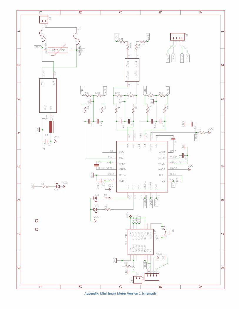
Mini Smart Meter
Before the second complex 20+ CT sub metering system is developed, it was decided
that a small “Smart Meter” would be designed in order to test several new ideas. This mini
Smart Meter would use only 2 CT’s to record, to a very high accuracy, the main power supply to
an entire household just as a utility installed Smart Meter would. It was to be as small and as
inexpensive as possible in order to easily rest inside a normal breaker box; specifically, a price
point around $50 and a PCB size smaller than a business card. The heart of the design uses a
Cirrus Logic CS5480 Three Channel Energy Measurement IC [7] along with an ESP8266 WI-FI
chip for data transmission to the internet. The CS5480 is an Analog Front End Energy
Measurement device which is preprogrammed to tabulate power data when attached to
sensors such as CTs. The ESP8266 simply reads power data from this chip and sends it over the
internet.
Images of the designed PCB are shown below. This PCB is being prepared for order from
PCBWay and assembly, programming, and testing will follow. The onboard analog circuitry was
designed based on the CS5480 reference designs provided by Cirrus Logic [2]. The small PCB,
only 2 inches by 2.7 inches, features full AC line isolation and protection with onboard power
supply, CS5480 chip with support circuitry, ESP8266 microcontroller with WI-FI connectivity,
and connections to two Dechang Electronics SCT-016 CTs for full 240V 120A service split phase
household power measurement. See appendix for full schematic.

15
Conclusion
Development of the metering systems discussed above was an extremely interesting
and rewarding engineering challenge; many aspects of engineering and business must be used
together to build a successful system. We began by describing the goals and initial design
decisions and progressed into technical aspects of those decisions. Some decisions, such as the
use of the LM2596 power supply due to low cost, led to unforeseen problems requiring time
and money to resolve later. Low cost components aren’t always a problem as demonstrated by
the ESP8266 WI-FI module and the low cost PCBWay PCB manufacturer. Making a WI-FI
enabled enabled system just a couple years ago would have been cost prohibitive as would
getting any PCBs professionally made. In reality, this is just the beginning of development for
these metering systems. The level of success upon completion of the Mini Smart Meter will
drive further design and business decisions with regard to the next version of the more
advanced circuit level sub metering system.
Mini Smart Meter PCB Design

16
References
[1] Dechang Electronics Co. (YHDC) Current Transformers
http://www.yhdc.com/en/product/category/Spilt-core-current-transformer/
[2] PJRC Teensy 3.1 Development Board
https://www.pjrc.com/store/teensy31.html
[3] Freescale MK20DX256VLH7 Microcontroller Data Sheet
https://www.pjrc.com/teensy/K20P64M72SF1RM.pdf
[4] Open Energy Monitor Project (EmonTX)
http://openenergymonitor.org/emon/modules/emonTxV3
[5] PCBWay Custom PCB Manufacturer
http://www.pcbway.com/
[6] Kerry D. Wong “LM2596 DC-DC Converter Module Testing”
http://www.kerrywong.com/2015/07/24/lm2596-dc-dc-converter-module-testing/
[7] Cirrus Logic CS5480 Three Channel Energy Measurement IC Datasheet
http://www.cirrus.com/en/pubs/proDatasheet/CS5480_F3.pdf
Appendix Items Follow Below
17
Appendix: PCB Version 1 Schematic
18
Appendix: Mini Smart Meter Version 1 Schematic