designing faster cmos sub-threshold circuits utilizing ......designing faster cmos sub-threshold...
TRANSCRIPT

Designing Faster CMOS Sub-threshold Circuits Utilizing Channel Length Manipulation
by
Farhad Ramezankhani, B. Sc., M. A. Sc.
A thesis submitted to the Faculty of Graduate and Postdoctoral
Affairs in partial fulfillment of the requirements for the degree of
Master of Applied Science
inElectrical and Computer Engineering
Ottawa-Carleton Institute for Electrical and Computer EngineeringCarleton University
Department of Electronics Ottawa, Ontario, Canada
September 2012
© 2012, Farhad Ramezankhani

1+1Library and Archives Canada
Published Heritage Branch
Bibliotheque et Archives Canada
Direction du Patrimoine de I'edition
395 Wellington Street Ottawa ON K1A0N4 Canada
395, rue Wellington Ottawa ON K1A 0N4 Canada
Your file Votre reference
ISBN: 978-0-494-93510-1
Our file Notre reference ISBN: 978-0-494-93510-1
NOTICE:
The author has granted a nonexclusive license allowing Library and Archives Canada to reproduce, publish, archive, preserve, conserve, communicate to the public by telecommunication or on the Internet, loan, distrbute and sell theses worldwide, for commercial or noncommercial purposes, in microform, paper, electronic and/or any other formats.
AVIS:
L'auteur a accorde une licence non exclusive permettant a la Bibliotheque et Archives Canada de reproduire, publier, archiver, sauvegarder, conserver, transmettre au public par telecommunication ou par I'lnternet, preter, distribuer et vendre des theses partout dans le monde, a des fins commerciales ou autres, sur support microforme, papier, electronique et/ou autres formats.
The author retains copyright ownership and moral rights in this thesis. Neither the thesis nor substantial extracts from it may be printed or otherwise reproduced without the author's permission.
L'auteur conserve la propriete du droit d'auteur et des droits moraux qui protege cette these. Ni la these ni des extraits substantiels de celle-ci ne doivent etre imprimes ou autrement reproduits sans son autorisation.
In compliance with the Canadian Privacy Act some supporting forms may have been removed from this thesis.
While these forms may be included in the document page count, their removal does not represent any loss of content from the thesis.
Conformement a la loi canadienne sur la protection de la vie privee, quelques formulaires secondaires ont ete enleves de cette these.
Bien que ces formulaires aient inclus dans la pagination, il n'y aura aucun contenu manquant.
Canada
Abstract
The Reverse-Short-Channel Effect in MOSFETs decreases the threshold voltage of a
transistor at longer channel lengths. Due to the exponential relation between the current
and threshold voltage in the sub-threshold region, increasing the channel length may
result in a maximum point in the current curve versus the channel length. Increasing the
channel length also increases the capacitances involve in the delay. A method based on
this behaviour is proposed to find the optimal channel lengths that maximize the Current-
over-Capacitance (CoC) of a transistor. The CoC method is extended to serial and
parallel transistor connections. The effectiveness of the CoC method is verified by
incorporating the obtained optimum channel lengths in ring oscillators consisting of
Inverter, NAND, NOR, and AOI gates. An improvement of 95% in the operation
frequency is achieved compared to the popular minimum-size sub-threshold circuits.
Using the optimum channel lengths in a 32-bit Carry-Look-Ahead adder shows about
50%, 20%, and 60% improvements in the delay, energy, and EDP, respectively compared
to the minimum-size version. The method is applied to the TSMC 65 nm, TSMC 90 nm,
IBM 130 nm, and TSMC 180 nm CMOS technologies.

In the Name of God,
the Compassionate, the Merciful

Acknowledgements
Whoever doesn ‘t thank others, hasn't indeed thanked God.
I wish to extend my utmost thanks to my thesis supervisor, Dr. Maitham Shams for
his guidance, support and patience. Working with him was a pleasant experience and the
time spent with him is an invaluable asset for me.
I would like to thank Professors Calvin Plett, Ralph Mason, Niall Tait, and Mustapha
Yagoub for their careful review and contributions to the thesis.
I would like to thank the staff members at the Department of Electronics,
especially, Blazenka Power, Anna Lee, Rob Vandusen, Nagui Mikhail, and Scott Bruce.
I would also like to thank my friends Dr. Reza Yousefi, Behzad Yadegari, Morteza
Nabavi, Xing Zhou, and Bai Zhanjun for their technical and moral assistance.
I would also like to thank CMC Microsystem and their technology partners for access
to the design tools used in the research for this thesis.
On a personal note, I wish to thank my lovely wife and daughter, for their love,
patience, and support throughout my studies.

Dedication
This dissertation is dedicated to ...
my wife, and our lovely daughter
for their unconditional love, patience, and support,
my father’s soul,
fo r believing in me and for his support and encouragement. His absence
is deeply felt.
Contents1 Introduction................................................................................................................1
1.1 Motivation............................................................................................................1
1.2 Thesis Objective.................................................................................................. 3
1.3 Thesis Organization............................................................................................4
2 Literature Review: ULP and Sub-threshold Circuits.............................................. 5
2.1 ULP Applications................................................................................................ 6
2.2 Why Sub-threshold?.......................................................................................... 10
2.3 Roadmap of Sub-threshold Circuits Design................................................... 14
2.4 Chapter Summary............................................................................................19
3 Background............................................................................................................. 20
3.1 MOSFET............................................................................................................20
3.1.1 Current....................................................................................................... 21
3.1.2 Threshold Voltage.................................................................................... 24
3.1.3 Capacitances..............................................................................................29
3.1.4 Leakage Currents.......................................................................................32
3.2 Quality Metrics of a Digital Circuit.................................................................33
3.2.1 Propagation Delay.....................................................................................33
3.2.2 Power Consumption................................................................................. 35
3.2.3 Energy Consumption................................................................................ 36
3.2.4 Voltage Transfer Characteristics............................................................. 38
3.3 Chapter Summery............................................................................................. 39
4 MOSFET Behavior in Sub-threshold Region....................................................... 40
4.1 Threshold Voltage Variation............................................................................ 40
4.2 Current Behaviour.............................................................................................44

4.3 MOSFET Capacitances.................................................................................... 49
4.4 Leakage Currents..............................................................................................54
4.5 Sub-threshold Slope..........................................................................................58
4.6 Chapter Summary.............................................................................................59
5 Delay Optimization in Sub-threshold Circuits....................................................... 60
5.1 Current-over-Capacitance (CoC).....................................................................60
5.2 Delay versus Channel Length.......................................................................... 64
5.3 Maximizing the Frequency of a RO.................................................................68
5.4 Primitive and Complex Logic Gates................................................................73
5.5 Chapter Summary............................................................................................. 79
6 Implications and Applications..................................................................................80
6.1 Increasing Vdd versus Channel-length Manipulation.................................... 80
6.2 32-bit CLA Adder............................................................................................. 83
6.3 Driving Large-Loads.........................................................................................86
6.4 Chapter Summary............................................................................................. 88
7 Conclusion................................................................................................................. 89
7.1 Summary............................................................................................................89
7.2 Contributions..................................................................................................... 91
7.3 Future work....................................................................................................... 91
List of References............................................................................................................ 93
VI

List o f Figures
Figure 2.1 Normalized static current for an inverter versus Vdd in 90 nm and 130 nm
technologies at minimum sizes.............................................................................................11
Figure 2.2 Static and Dynamic energy (a) and total energy (b) versus Vdd for 29-inverter
RO in 130 nm technology at minimum size..........................................................................12
Figure 2.3 Energy vs. Frequency (top) and I0J I 0« ratio vs. V d d (bottom) simulated in
130 nm technology.................................................................................................................. 15
Figure 3.1 structure of an n-channel MOSFET (NMOS).................................................... 20
Figure 3.2 Current vs. Fgs in logarithmic scale.....................................................................23
Figure 3.3 Cross-section of a MOS transistor along the width showing LOCOS (a) and
STI (b) isolation and their effect on threshold voltage.........................................................25
Figure 3.4 Charge sharing between source/drain depletion regions and the channel
depletion region resulting in threshold roll-off.................................................................... 26
Figure 3.5 DIBL in a short-channel device...........................................................................27
Figure 3.6 HALO doping effects on threshold voltage of short and long-channel
transistors.................................................................................................................................28
Figure 3.7 MOSFET Capacitances........................................................................................29
Figure 3.8 (a) Representation of MOSFET capacitances, (b) decomposition of
source/drain junction capacitance to bottom and sidewall components............................. 29
Figure 3.9 Dependence of gate capacitance of an NMOS transistor to gate voltage 31
Figure 3.10 Propagation delay for an inverter driving another inverter with input and
output signals approximated as ramps...................................................................................34
Figure 3.11 Minimum energy point..................................................................................... 37
Figure 3.12 Typical inverter VTC......................................................................................... 38
Figure 4.1 Threshold voltage versus the channel width at Lm =120 nm(left), and
threshold voltage versus the channel length at lFmin=160nm (right) for IBM 130 nm
technology............................................................................................................................... 41
Figure 4.2 Threshold voltage versus W at Vdd=0.2 V for a PMOS transistor in different
technology nodes at L=Lm ....................................................................................................42

Figure 4.3 Threshold voltage versus W at F d d= 0 .2 V for an NMOS transistor in
different technology nodes at L=Lm .................................................................................... 42
Figure 4.4 Threshold voltage versus L at F dd~ 0 .2 V for a PMOS transistor in different
technology nodes at W=Wmi„.................................................................................................43
Figure 4.5 Threshold voltage versus L at F dd= 0 -2 V for an NMOS transistor in different
technology nodes at W=Wmm.................................................................................................43
Figure 4.6 Super-threshold current for a PMOS transistor at F dd= 1 V versus L and W, in
IBM 130nm CMOS (NMOS transistor shows the same behavior).....................................44
Figure 4.7 Top figure shows normalized 1/Z and exp(Vcs — Vth) /n v T) factors
individually plotted versus L. The bottom figure shows normalized ML X exp(VGS —
Vth) /n v T) and normalized current at Fdd=0.2 V for TSMC 65 nm LP CMOS kit for a
PMOS-lvt transistor at W=Wmin=120 nm.......................................................................... 45
Figure 4.8 Top figure shows normalized 1/Z, and exp(VGS — Vth) /n v T) factors
individually plotted versus L. The bottom figure shows normalized 1/ZX exp(VGS —
Vttl) /n v T) and normalized current at Fdd=0.2 V for TSMC 65 nm LP CMOS kit for a
PMOS-svt transistor at VF=VFmm=120 nm.......................................................................... 46
Figure 4.9 Sub-threshold current versus W in different technology nodes at F d d= 0 .2 V
and Zmjn.................................................................................................................................... 47
Figure 4.10 Sub-threshold current versus L in different technology nodes at F dd= 0 .2 V
and lFmjn................................................................................................................................... 48
Figure 4.11 Sub-threshold current versus the channel length for an NMOS transistor in
IBM 130 nm technology at Wmi„. The maximum point becomes smaller as the supply
voltage increases..................................................................................................................... 49
Figure 4.12 L\max versus FDd at Wmin................................................................................... 50
Figure 4.13 Gate capacitances versus gate voltage for an NMOS transistor in IBM
130 nm for two different Fds- Cgg is equal to the sum of the other three capacitances. ..51
Figure 4.14 Drain-body junction capacitance versus Fds for an NMOS in IBM 130 nm
technology at two different Fss............................................................................................. 52
Figure 4.15 Gate and drain capacitances versus the channel width and channel length for
an NMOS in IBM 130 nm at F ds^ F ds^ ^ V.......................................................................53

Figure 4.16 Ctotai versus the channel length (left) and versus the channel width (right) for
an NMOS in IBM 130 nm for two sets of voltages that are used in delay modeling and
estimation.................................................................................................................................53
Figure 4.17 Test benches used for leakage currents measurement......................................55
Figure 4.18 I0« and /on versus L (@ lTmjn) left figure, and versus W (@ i min) right figure
for PMOS transistor in IBM 130 nm technology at Fdd=0.2 V.......................................... 56
Figure 4.19 7on / h n versus L and versus W (@Lmj„) at FDd=0.2 ..........................57
Figure 4.20 Sub-threshold slope versus W (@ Zmjn) (left) and versus L (@ JFmjn)(right)
for NMOS and PMOS transistors.......................................................................................... 58
Figure 5.1 An inverter driving an identical inverter. High-to-low and low-to-high
transitions are illustrated.........................................................................................................62
Figure 5.2 CoC versus L for NMOS and PMOS transistors in IBM 130 nm technology at
Fdd= 0 .2 V ........................................................................................................................................... 62
Figure 5.3 CoC versus L for PMOS-lvt in TSMC 65 nm LP at two different supply
voltages.................................................................................................................................... 63
Figure 5.4 Lcocmax versus Fdd................................................................................................ 64
Figure 5.5 Delay versus Lp and Ln for an inverter driving an identical inverter. 3D plot
(top) and contour plot (bottom) simulated in IBM 130 nm at Fdd=0.2 V .........................65
Figure 5.6 Delay contours versus Lp and Ln in TSMC 65 nm at Fdd=0.2 V......................66
Figure 5.7 Delay versus supply voltage measured for three different sets of transistors
sizing........................................................................................................................................67
Figure 5.8 VTC for an inverter plotted for four sets of channel lengths in 65 nm at
Fdd=0.2 V. Both NMOS and PMOS transistors are “lvt” types......................................... 71
Figure 5.9 A RO with NAND2 logic gates connected in its worst-case scenario 73
Figure 5.10 Pull-down (a) and pull-up (b) networks for a NAND2 logic gate connected in
the worst case scenario........................................................................................................... 74
Figure 5.11 LcoCmax versus Fdd for different connection topologies of transistors used as
a building blocks for logic gates............................................................................................78
Figure 6.1 Energy per operation and frequency vs. Fdd for a 29- INV RO in the 65 nm
technology at Z,mjn=60 nm.......................................................................................................80

Figure 6.2 Energy per operation and frequency vs. Vdd for a 29- INV RO in the 65 nm
technology at !Fmin=120 nm................................................................................................... 81
Figure 6.3 Energy per operation and frequency vs. Vdd for a 29- INV RO in the 65 nm
technology at JFmjn=120 nm................................................................................................... 83
Figure 6.4 EDP versus Vdd for a 29-INV RO simulated for four different sets of transistor
sizes in the 65 nm technology................................................................................................ 84
Figure 6.5 Block diagram for a 4-bit CLA adder [15]......................................................... 84
Figure 6.6 Driving a large load with a chain of three inverters...........................................87
Figure 6.7 Output signal of a chain driving a large load at Fdd=0.2 V and Wmin=120 nm
in the 65 nm technology......................................................................................................... 87
x

List o f Tables
Table 2.1 Low-power techniques for high-performance digital circuits [19]...................... 7
Table 2.2 Micro-sensor networks applications [17].............................................................. 8
Table 2.3 Example of power harvesting mechanism and their typical power densities...... 9
Table 2.4 Leakage power savings from voltage reduction (constant leakage current)...... 11
Table 2.5 Summary of Sub-threshold papers........................................................................ 18
Table 3.1 Approximation for MOSFET capacitances [80]..................................................31
Table 4.1 The leakage currents for NMOS and PMOS transistors in each technology at
their minimum acceptable sizes............................................................................................. 55
Table 5.1 Delay measured for three different sets of transistor sizing at Fdd=0.2 V........ 67
Table 5.2 Frequency for a RO with 9 and 29 inverters simulated for two different sets of
transistor sizing at Fdd=0.2 V................................................................................................69
Table 5.3 Frequency in a 29 inverter RO simulated for three sets of channel lengths at
Fdd=0.2 V................................................................................................................................70
Table 5.4 Frequency for a 29 inverter RO in different supply voltages for three different
sets of channel lengths for TSMC 65 nm LP........................................................................70
Table 5.5 Noise margins for an inverter in three sets of channel length compared to that
of the minimum size inverter. Energy per cycle and frequency operation of a 29 inverter
RO compared for these four sets of channel lengths............................................................72
Table 5.6 LcoCmax for transistor configuration shown in Figure 5.10 at Fdd=0.2 V...........74
Table 5.7 LcoCmax for different combinations of MOSFETs at Fdd-0.2 V.........................75
Table 5.8 Simulation results for RO consisting of 29 of each logic gate for four sets of
channel lengths at Fdd= 0.2 V................................................................................................ 77
Table 6.1 Simulation results for a 32-bit CLA adder in the 65 nm technology at Fdd=0.2.
..................................................................................................................................................85
Table 6.2 Simulation results for a three-inverters chain driving a large load at Fdd= 0.2 V.
86
xi

Table 6.3 Simulation results for a three-inverters chain driving a large load at Fdd=0.2 V.
In each intermediate node three minimum-size inverters are connected in parallel as off-
path logic gates........................................................................................................................88

List of SymbolsSymbol Definition Unit
05 Surface Potential V
Cjo Junction Capacitance at zero bias F
n Built-in potential V
eSi Permittivity of Silicon F/m
Cox Vacuum Permittivity F/m
M Charge Mobility cm2/(V.s)
fin Electron mobility cm2/(V.s)
Mp Hole Mobility cm2/(V.s)
C Capacitance F
Cav Average Capacitance F
Cdep Depletion Layer Capacitance per Unit Area F/cm2
C gg Total Gate Capacitance F
C db Drain to Body Capacitance F
C sb Source to Body Capacitance F
Q Junction Capacitance per Unit Area F/cm2
Cjsw(Cjswg) Side-wall Junction Capacitance per Unit Length F/cm
Cox Field Oxide Capacitance F/cm2
Edyn Dynamic Energy Consumption J
Es t Static (Leakage) Energy Consumption J
E t Total Consumed Energy J
Ids Drain-Source Current A
Idsat Saturation current A
Igate Gate Leakage Current A
Ijunct Source and Drain Junctions Leakage Current A
I leakage Leakage Current A
iNav NMOS Transistor Average Current A
/off Transistor “O ff’ Current A

Ion Transistor “On” Current A
lon-av Average ON current A
IPav PMOS Transistor Average Current A
Isc-av Average Short-Circuit Current A
hub Sub-threshold leakage current A
L Transistor Length m
LcoCmax Channel Length Resulting in Maximum CoC m
L d Lateral Diffusion m
I>Dmin Channel Length Resulting in Minimum Delay m
I Emin Channel Length Resulting in Minimum Energy m
Lfmax Channel Length Resulting in Maximum Frequency m
U m a x Channel Length Resulting in Maximum Current m
M j Junction Grading Coefficient
n Sub-threshold Slope Factor
Nsxib Substrate Doping cm
P c Fitting Parameter in the Alpha Power law
P dyn Dynamic Power Consumption W
Psc Short-Circuit Power Consumption W
PsT Static Power Consumption W
Psw Switching Power Consumption W
P v Fitting Parameter in the Alpha Power law
Qdep Depletion Charge per Unit Area C/<
s Sub-threshold Slope mV
tax Gate Oxide Thickness m
tp Propagation Delay s
tphl High-to Low Propagation Delay s
tplh Low-to High Propagation Delay s
Vdd Supply Voltage V
Vds Drain-Source Voltage V
Vdsat Saturation Voltage V
xiv

Vfb Flat-band Voltage V
Vm Gate-Source Voltage V
Vr Revers Bias On Junction V
vt Thermal Voltage V
V,h Threshold Voltage V
Vth„ NMOS Transistor Threshold Voltage V
Vthp PMOS Transistor Threshold Voltage V
W Transistor Width m
WdeP Width of Depletion Region under the Gate m
a 1)Switching Activity Factor
2) Velocity Saturation Index
(pst Surface Potential at Threshold Condition V
/? Transconductance A/V2
Vm Minimum input voltage to an inverter that is V
considered a logic “1”
Vn Maximum input voltage to an inverter that is V
considered a logic “0”
Foh Minimum Output Voltage of an Inverter that V
Indicate a logic “1”
Vol Maximum Output Voltage of an Inverter that V
Indicate a logic “0”
xv

List of AbbreviationsAbbreviation Definition
CoC Current-over-Capacitance
CPL Complementary Pass-Transistor-Logic
DIBL Drain Induced Barrier Lowering
DVL Dual-Value-Logic
EDP Energy Delay Product
GND Ground
INWE Inverse Narrow Width Effect
LOCOS Local-Oxidation of Silicon
lvt Low-voltage-threshold
MOSFET Metal-Oxide-Semiconductor Field Effect Transistor
NMOS n-Channel MOSFET
NWE Narrow Width Effect
PDP Power Delay Product
PMOS p-Channel MOSFET
PTL Pass-Transistor-Logic
RSCE Reverse Short Channel Effect
SCE Short Channel Effect
SNM Static Noise Margin
SRAM Static Random-Access Memory
STI Shallow Trench Isolation
svt Standard-voltage-threshold
UDVS Ultra-Dynamic-Voltage-Scaling
ULP Ultra-Low-Power
VTC Voltage Transfer Characteristics
xvi
1 Introduction
In the area of VLSI system design, considerable attention has been given to the
design of high-performance processors and memories. However, in recent years, the
demand for Ultra-Low-Power (ULP) applications has grown significantly. This
tremendous demand has mainly been due to the fast growth of portable electronics
market. Users are interested in having their portable devices operating for longer times
per charge. Hence, in these applications, energy-efficiency is of primary importance.
Several approaches have been explored by researchers to reduce the power
consumption in a digital circuit. The most straight forward method to reduce the power
consumption is utilizing supply voltages lower than the nominal ones. According to [1],
operating at supply voltages less than the threshold voltage of transistors, called sub
threshold operation, reduces the energy consumption by an order of magnitude. In
addition, the minimum energy operation, i.e., operating at a supply voltage where the
energy consumption is at its lowest, also occurs in the sub-threshold region [1]. This,
however, causes drastic performance degradation due to significant decrease in the
driving current.
In some ULP applications such as biomedical devices, where operation frequencies
are low and the main challenge is to keep the energy-consumption level as low as
possible, sub-threshold design is the best solution. However, the challenge is to widen the
span of the operation frequency of sub-threshold circuits to the level of mid-performance
applications with no or minimal cost in energy.
1.1 Motivation
A number of projects have been performed to make the sub-threshold circuits more
suitable for higher frequency applications. These projects spread from the transistor-level
to system-level solutions [2] [3] [4] [5] [6] [7].
1

An effective way for enhancing the speed of sub-threshold circuits is to manipulate
the dimensions of the transistors. Two of my teammates have chosen to study the effect
of the transistor channel width on the speed of sub-threshold circuits. They came up with
valuable results in their Master’s theses [6] [7]. They proposed methods on finding
optimum channel widths that improve the delay drastically. They also introduced a novel
technique on using several parallel-transistors instead of a single wide transistor. They
applied their methods to different types of circuits, from simple Ring Oscillators (RO), to
a more complicated 32-bit Carry-Look-Ahead (CLA) adder, and the results were
considerable.
However, I decided to look into the problem from another aspect. I decided to study
the effect of the channel length on the sub-threshold circuits’ behaviour. I obtained this
idea when I was doing my first studies on the feasibility of Pass-Transistor-Logic (PTL)
design in this mode of operation. I came across several papers that had the same idea but
with a number of major drawbacks.
The first paper that suggests channel length manipulations in the sub-threshold
design improvement is [8]. In this paper authors have utilized Reverse-Short-Channel-
Effects (RSCE) in their designs. This work suffers from a number of shortcomings. First,
their PMOS transistor is apparently improperly biased. I biased a PMOS transistor in
TSMC 130 nm technology kit and plotted the current versus the channel length through
simulation in Cadence CAD tool. I found that if we bias the PMOS transistor in a wrong
way, the plot will be the same as the current plot presented in the paper. This mistake
resulted in using a non-optimal channel length for PMOS transistors. Second, the
derivative obtained for the current with respect to the channel length is mathematically
incorrect. I found this mistake by calculating the derivative by hand. In addition this
result is not carried on in designing discussed circuits in the paper. Third, although it is
known that minimum-sized sub-threshold circuits perform competitively well, no
comparison is reported between their proposed circuits and minimum-size transistor
circuits. Fourth, the authors applied their findings to some ISCAS test benches and
showed that the performance and power consumption improved. ISCAS test benches use
transistor sizing that are more suitable for super-threshold operation, where the Inverse-
Narrow-Width Effect (INWE) and RSCE are not observed.
2

The second paper that uses longer channel length in the sub-threshold region is [9].
In this work, the channel length is manipulated to achieve the minimum-energy
consumption for power supplies between 300 to 700 mV that cannot be usually
considered as sub-threshold operation modes. This work does not address any speed
improvements and comparisons to circuits with minimum-size transistors.
There are several other papers that study the channel length effect on the performance
and energy improvement in the sub-threshold region, such as [2] [10] [11]. In none of
them a methodology to find the optimum channel length minimizing the delay is
presented.
Accordingly, I decided to study the effect of channel length manipulation on the
behaviour of a transistor in the sub-threshold region, and utilize the results in designing
digital circuits block. In this work, my main research focus is on the frequency and delay
optimizations. However, in some cases where there is a need to discuss the energy
consumption, it is addressed as well.
1.2 Thesis Objective
This thesis follows the objectives listed below.
• To study the behaviour of a MOSFET in the sub-threshold region with respect
to its dimensions.
• To perform a comparative study of the effects of the channel width and
channel length manipulation on important parameters of MOSFETs such as
the threshold voltage, current, capacitances, sub-threshold slope, and on-
current to off-current ratio (7on/ /off)-
• To exploit the sub-threshold behaviour of transistors to find the optimum
channel length for minimizing the delay.
• To propose a design methodology for delay optimization for sub-threshold
circuits through transistors’ channel length manipulation.
• To apply the methodology to design some common circuits and verify its
effectiveness.
3

1.3 Thesis Organization
After this introductory chapter, the second chapter presents a historical background
of the origin of ULP applications, challenges, and the offered solutions for them. Sub
threshold operation is introduced as the best candidate to solve the problems of many
ULP circuits. Challenges in designing a sub-threshold circuit are addressed and the
potentials of different research areas are presented.
The third chapter covers the background information that is needed in studying the
transistor behaviour study and digital circuits figure of merits.
In Chapter 4, we present a detailed study on transistor’s important parameters with
respect to its dimensions, such as the threshold voltage, current, capacitances, and sub
threshold slope.
In Chapter 5, based on the current and capacitance behaviour presented in Chapter 4,
the Current-over-Capacitance (CoC) method is presented. First, the CoC method is
developed for one transistor to find its optimum channel length. Then, this method is
extended for serial and parallel combinations. The effectiveness of the optimum channel
lengths is verified by incorporating them in different ROs.
In Chapter 6, some applications of our proposed methodology are presented. The
obtained optimum channel lengths in Chapter 5 are used in a 32-bit CLA adder and a
chain of inverters driving a large load. Improvements in both the delay and energy are
reported.
Finally, Chapter 7 presents the concluding remarks.
4

2 Literature Review: ULP and Sub-threshold
Circuits
When the first integrated electronic circuit built on a single slice of Germanium by
Jack Kilby in 1958 at Texas Instruments in Dallas, nobody knew that this invention will
revolutionize electronics market, and consequently the life of everyday [12]. Now,
several decades later, his invention known as Integrated Circuits (ICs), is being used in a
wide range of applications, from high-technology space crafts to small toys for kids.
The ICs world is accustomed at this point to following the Moore's Law. In 1965,
Gordon Moore observed that the number of transistors that can be most economically
manufactured on a chip doubles every 18 months [13]. Since that time, the IC industry
has maintained the astonishing exponential trend, which Moore first observed, by
continuing to scale down the size of transistors to have faster, cheaper, and less power
consuming ICs (i.e., Dennard’s Scaling Law) [14].
The traditional goal has been to reduce the minimum feature size by 30% with each
new technology. This scaling, theoretically, results in 30% and 50% reduction in logic
gate’s delay and chip area, respectively. Likewise, active power should decrease for a
given circuit due to smaller transistors and lower supply voltages [3]. Obviously, this
scaling cannot go on forever because transistors cannot be smaller than atoms. Dennard
Scaling Law has already begun to slow. In 1990s, experts agreed that the scaling would
continue for at least a decade, but in 2009, they predicted that Moore’s Law will continue
for another decade [15].
Despite the reduction of power consumption in each individual transistor caused by
scaling, the total power consumption per chip has drastically increased due to the
exponential growth in the number of integrated devices per chip and the increase in the
clock frequency. A power consumption of 8 W is reported for an Intel Pentium CPU
operating at 75 MHz, whilst the power consumption is increased to 150 W for a newer
CPU generation, Core 2 Extreme QX9775 operating at 3.2 GHz [16]. This increase in
5

the power consumption that is noticeable in high-performance applications such as
microprocessors, introduces new challenges to both fabrication and circuit design
engineers, like the need for special packaging for the quick removal of the produced heat
inside the chip and designing more stable circuits with respect to temperature variations
inside the chip. Therefore, exploring design methodologies for low-power circuit is of
great importance.
In addition to the heat problem, demands for portable battery-operated devices have
increased significantly over the last decades. Taking a laptop as an example, consumers
are strongly calling for laptops with lower price but much longer running time per charge.
Furthermore, in some applications like implantable biomedical devices, where changing
the battery needs a surgery, a small battery should work for tens of years inside the
patient’s body. Also, while the number of transistors integrated on a chip doubles every
18 months based on the Moore’s Law, the capacity density of batteries doubles only
every 10 years [17]. Hence, the energy consumption becomes a bottleneck rather than the
performance for many applications.
All of this attention to the power and energy consumption in circuit design has
created a significant research potential for minimizing or at least reducing the energy or
power consumption. In the following, first, a brief history of ULP applications is
presented. Then, the sub-threshold operation is introduced as a solution for most ULP
applications. The challenges in the design of sub-threshold circuits are discussed next.
Thereafter, the previous related sub-threshold work is reported to address how
researchers have faced these challenges and what are the drawbacks of their researches.
2.1 ULP Applications
The first ULP application goes back to 60’s when the Centre Electronique Horloger
Neuchatel developed an electronic wristwatch that consuming less than 30 pA from a
1.3 V supply voltage [18]. This was the only ULP application for 30 years, until a couple
of decades ago that the new class of ULP applications were introduced. ULP applications
are categorized into high performance and low to medium performance. In the first
6
group, performance and power (energy) consumption have the same level of importance.
Table 2.1 summarizes digital circuit techniques in these kinds of applications.
Table 2.1 Low-power techniques for high-performance digital circuits [19].
Design hierarchy Reported low-power digital techniques
1 - Using more efficient DSP algorithms to
Algorithmic level eliminate unnecessary computation and reduce
the number of computation
1- ISA extension
2- Scenario based mapping, rescheduling, etc.
3- Preserving data correlation and reference
Mapping and architecture levellocality, reducing memory access
4- Common expression elimination, pre-
computation, etc.
5- Using suitable pipelining and parallelism,
enabling low supply voltage/frequency
1- Multiple supply voltage (MVS)
2- Dynamic voltage scaling (DVS)
3- Dynamic voltage-firequency scaling (DVFS)
System level 4- Multiple clock domains
5- Dynamic- Variable threshold voltage (adaptive
body biasing)
6- Sleep and power down modes
1 - Power gating, clock gating
2- Logic sizing and re-structuring
Circuit level 3- Adiabatic logic circuits
4- Low power SRAM and DRAM
5- Power efficient DC-DC level converter
1- Multiple threshold CMOS
Device level2- Low temperature CMOS
3- Silicon-on-Insulator
4- Low power packaging
7

In the second group of ULP applications power and more specifically energy is a
fundamental constraint. These ULP applications do not require the ultimate performance
of high-end processors. Among them, Radio-Frequency Identifier (RFID) tags and
Micro-sensor networks are attracting more attentions. RFID tags are used to wirelessly
identify an object, an animal or a person [20]. Micro-sensor networks refer to the physical
hardware that provides sensing, processing, and wireless communication. These networks
consist of thousands of distributed nodes that sense and process data and send it to the
end-user. Micro-sensors are used in habitat monitoring [21], environment observation and
forecasting systems [22], structural monitoring [23], and health monitoring [24] [25].
Other examples for micro-sensor networks include automotive industries, military
applications for early biological and chemical weapons detection, and traffic density
monitoring in cities. Table 2.2 lists some micro-sensor networks applications. For each
application, the associated sampling rates (in Hz) and the sample precision (in bits per
sample) are also indicated.
Table 2.2 Micro-sensor networks applications [17]
Application Sample Rate (in Hz) Sample Precision (in bits)
Body temperature 0.1-1 8
Heart Rate 0.8-3.2 1
Blood Pressure 50-100 8
BiomedicalElectro-Enccephlo-
Graph (EEG)100-200 16
Applications Electro-Cardio-Graph100-250 8
(ECG)
Electro-Myo-Graph
(EMG)100-5000 8
Hearing Aids 15000-44000 16
Ambient light level 0.017-1 16
Climate Ambient noise level 0.017-1 16
Monitoring Barometric pressure 0.017-1 8
Wind direction 0.2-100 8
Automotive Engine temperature 100-150 16
Industry Tire pressure 100-150 16
8

The low-power techniques listed in Table 2.1 are not effective enough for the
applications listed in Table 2.2. These entire applications share a common characteristic:
their low computational load, and a common constraint: tiny power or energy
consumption. Indeed, these applications either have to operate for a long time on small
batteries or harvest energy from the ambient.
In some micro-sensor networks applications, especially biomedical applications,
where the micro-sensor should be implanted inside the patient’s organ, the battery have to
be very small and long-lasting. As a reference, a 1 cm Lithium battery has 1.5 KJ of
capacity, which means it can deliver 10 pW of power over five years [26]. In some other
kinds of micro-sensor networks, they gain their energy by harvesting it from the ambient.
Table 2.3 lists the typical power harvesting mechanisms and their typical delivered power
densities. The power available from these sources depends on the area of the power
source and environmental conditions at any given time. It is reasonable to expect tens of
pW to be harvested from the ambient energy. Therefore, according to the capacity of the
batteries and power harvesting mechanisms, micro-sensor nodes must keep their average
power consumption in the 10-100 pW range [27],
Table 2.3 Example of power harvesting mechanism and their typical power densities.
Mechanism Power Density (pW/em2)
Electromagnetic Vibration [28] 4
Piezoelectric Vibration [29] 500
Electrostatic Vibration [30] 3.8
Thermoelectric [31] 60
Solar-Direct sunlight [32] 3700
Solar-Indoor [32] 3.2
Notice that, the important figures of merit to consider are different, depending on the
energy or power source. In battery-operated systems, the energy to perform an operation
has to be low enough to have a reasonable battery life span. While, for environment
energy harvesting systems, where the available energy that can be harvested is limited but
9

ample time is available, the power has to be minimized. Because the energy source
remains available, the fact that an operation takes more energy is less important than
keeping the circuit power below the available constraint.
2.2 Why Sub-threshold?
As presented in the previous section, there are many ULP applications that need
small battery size and small amount of produced heat, especially in biomedical
applications to prevent any damage to the tissues [24]. It seems that lowering the supply
voltage is the best solution to meet the requirements of such applications. Both energy
and power consumption depend on the supply voltage, i.e., lowering the power supply
will decrease both. Now, there is a question to be answered. What is the minimum limit
of the power supply? Can we reduce the supply voltage indefinitely?
Swanson and Meindl studied the limits of voltage scaling in the early 1970s [33].
They showed in theory that an inverter could maintain its functionality till Tdd- 4vj,
where Fdd is the supply voltage and vj is the thermal voltage, which is 26 mV at room
temperature. Soon after, they implemented a RO and found 100 mV as the minimum
practical limit for the supply voltage [34]. In [35], the authors claimed a minimum
operational voltage of 48 mv, theoretically, and verified it by SPICE simulations in the
0.18 pm technology.
Operating in this new range of supply voltage, which is less than transistors’
threshold voltage, is referred as Sub-threshold operation. This mode of operation involves
using a supply voltage in the 0.2 to 0.4 V range that is substantially lower than the
nominal supply voltage (which fall to in the 0.9 to 1.2 V range) for the modem CMOS
technologies.
Decreasing the power supply reduces both the active and static consumed power by a
circuit. The static or leakage power ( P st) in a circuit is given by
P s t = F d d X /u a k (2 - 1)
where 7uak is the leakage current. Lowering the supply voltage is the most
straightforward way of reducing the leakage power consumed by the circuit. For
10

example, if we reduce Fdd from its nominal value in the 130 nm technology, Fdd= 1-2 V,
to a Fdd in the sub-threshold region, e.g., Fdd=0.2 V, Pst decreases six times, providing
that the leakage current is constant. Table 2.4 shows a saving in Pst by 2.25-6 times, only
from the supply voltage reduction assuming a fixed leakage current.
Table 2.4 Leakage power savings from voltage reduction (constant leakage current).
Nominal Fdd (V)
Sub-threshold FDD (V) 0.9 1 1.1 1.2
0.4 2.25X 2.5X 2.75X 3X
0.3 3 X 3.3X 3.7X 4X
0.2 4.5X 5X 5.5X 6X
Since lowering the supply voltage also decreases the leakage current, in the real case,
savings in the static power by reducing Fdd are even more than those reported in Table
2.4. Figure 2.1 shows a five times reduction in the leakage current when the supply
voltage scales down from 1.1 V to 0.2 V. Combining the changes in the leakage current
with the results of Table 2.4 leads to a saving of 6.5 to 30 times in P s t -
5.5
4.5
o>
3.5
2.5
130 nm 90 nm
1.5
0.1 0.2 0.3 0.4 0.5 0.6 0.7 0.8
vddMFigure 2.1 Normalized static current for an inverter versus VDD in 90 nm and 130 nm technologies at minimum sizes.
11

One of the side effects of operating in the sub-threshold region is a significant
increase in the delay, due to the very small on-current. Delay in sub-threshold circuits is
orders of magnitude more than that of super-threshold circuits. However, they are still
useful in many ULP applications with low speed, as described in Section 2.1.
Due to the significant increase in the delay for circuits operating in the sub-threshold
region, the static or leakage energy ( E st ) increases as the supply voltage reduces. The
Static energy depends on how fast an operation takes place. In spite of the static power
reduction by lowering the supply voltage, the static energy increases (Figure 2.2 (a)). On
the other hand, since the dynamic energy is proportional to Fdd , it decreases
quadratically by lowering Fdd (Figure 2.2 (a)). The total energy, which is the sum of the
static and dynamic energies, decreases until the static energy becomes dominant and
creates a minimum point, as illustrated in Figure 2.2(b). This minimum-energy point
consistently occurs at the sub-threshold region [1] [36] [37].
x 10.-1? x 10 5
-14 x 10.-H5 3.5
E dyn+ E st
0 0.5 1.5
(a) (b)
Figure 2.2 Static and Dynamic energy (a) and total energy (b) versus V0D for 29-inverter RO in 130 nm technology at minimum size.
12

When Vittoz and Fellrath demonstrated the first analog circuit operating in the sub
threshold region at the 1976 European Solid-State Circuits Conference (ESSCIRC) [38],
the audience suggested that such circuits could not be reliable, as they operate with the
leakage current [39]. Thanks to the wrist-watch application, analog sub-threshold circuits
received more attention than digital sub-threshold circuits until the 1999 IEEE/ACM
International Symposium on Low-Power-Electronics and Design (ISLPED), where
Soelemen and Roy showed that operation of CMOS and pseudo-NMOS logic gates down
to 0.3 V leads to nearly two orders of magnitude power-delay product (PDP) saving in a
0.35 pm technology [40].
After [1] and [40], despite the all challenges -to be introduced later- in the sub
threshold circuits design, ULP sub-threshold circuits came out of the shadow and turned
into a vibrant research area in digital electronics. Till 2008, a decade after Soeleman’s
first paper in sub-threshold logic, there had been numerous successful sub-threshold
circuits implementations. Among the most advanced ones was a complete sub-threshold
microcontroller with an embedded SRAM and a DC-DC converter in a 65 nm technology
for biomedical applications designed in collaboration between MIT and Texas Instrument
[4]-
Although sub-threshold circuits originated for low-performance ULP applications, it
does not mean that they are not applicable in high-performance circuits. When high-
performance systems enter into the sleep mode to reduce the power consumption, some
circuits are still operating to monitor the status of the whole system to decide the wake up
time. One existing example is a standby leakage-reduction system that uses a feedback
loop and Canary SRAM cells to the set standby Fdd to minimize the leakage while
protecting the data in the SRAM [41]. Sub-threshold operation seems ideal for the sleep
mode circuits.
Additionally, many high-performance systems, such as microprocessors used in
laptops and smart phones, spend a large fraction of time with a smaller operational load
than their maximum operational load. Sub-threshold operation can be used during these
periods for the background computation that do not require high throughputs. This can
reduce on-die temperature and energy cost. One practical implemented circuit is a
13
combination of multi-Fdd with a small set of power switches to perform a flexible
dynamic voltage scaling [42] [43].
Finally, the growing potential of large-scale microprocessors combined with their
power constraints, which is becoming more prominent for these systems than before, (as
their operation frequency grows rapidly) has opened a new research path for the sub
threshold and near-threshold computing in parallel architectures such as many-core
microprocessors [44].
2.3 Roadmap o f Sub-threshold Circuits Design
Sub-threshold operation seems the best match for ULP applications as their usage are
daily increasing. However, there are some challenges that sub-threshold designs face.
Sub-threshold researches are focused on overcoming these challenges. These challenges
are discussed in the following.
1- When the supply voltage drops below the threshold voltage, the transistor current
still remains above zero. A nonzero gate-to-source ( F g s) voltage that is less than
transistor threshold voltage still produces a current that is larger than the off-
current, /0fr ( i.e., the transistor current when Fbs=0 V). This finite ratio of the on-
current, 70n, to 70ff lets sub-threshold digital gates behave statically in a similar
fashion to the super-threshold gates. However, their transient behaviour is much
slower than the super-threshold ones, due to the small drive currents. The
frequency of operation in the sub-threshold region is orders of magnitude smaller
than that of the super-threshold region. For instance, Figure 2.3 (top) shows that
reducing the power supply from its nominal value, 1.1 V, to the sub-threshold
value, 0.2 V, reduces the operating frequency by three orders of magnitude for
about 20 times reduction in the total energy per operation.
2- As shown in Figure 2.3 (bottom), the I0J I0ff ratio reduces about three orders of
magnitude when the supply voltage reduces from its nominal value to the sub
threshold value. This reduction in the / on/ / o f f ratio can lead to reliability
problems. For example, for certain gates with parallel leaking path (e.g., NOR
gates) or in keepers, degraded I0J /0ff ratio results in a bad functionality.
14

3- Process-Voltage-Temperature (PVT) variations that become more prominent in
modem CMOS technologies, affect the transistor threshold voltage and
consequently the current, both in the super-threshold and sub-threshold regions.
However, this effect is more obvious in the sub-threshold region because of the
exponential relation between the current and threshold voltage (i.e., 1D oc
exp(Vcs — Vth), where V& is the threshold voltage of transistor).
Despite the mentioned challenges, researchers have successfully developed
techniques to build relatively fast and robust sub-threshold digital circuits ranging from
small gates and SRAMs to processors. Overcoming these challenges needs a wide
collaborative research at every design hierarchy level. Some of the important research
topics are listed below.
• Device Optimization for Sub-threshold Operation: Standard transistors are
super-threshold transistors and optimized for operation in their nominal
.-13
FDD=1.1 V
E= 32 0, f= 665 MHz
.-14 Kdd=0.2 V
E= 1.4 fJ, f= 446 KHzt l l t l
UJ
.-15
f( Hz)
10
410
.210
)°l_______' r_______ I_______r • •______ I_______ I_______L0.1 0.2 0.3 0.4 0.5 0.6 0.7 0.8 0.9 1
101.1
Figure 2.3 Energy vs. Frequency (top) and I0Jhn ratio vs. V0D (bottom) simulated in 130 nm technology.
15

supply voltages for high-performance applications. It is an established fact
that the doping profile and level in conventional transistors are designed to
mitigate the Short-Channel-Effects (SCE), e.g., punch-through. However, In
the sub-threshold region the supply voltage is small and SCEs are not
significant. It means that many of the process steps to produce special drain
and source region or channel doping tuning are not any more necessary for
transistors operating in the sub-threshold region [45]. On the other hand, the
gate oxide thickness should be optimized for this region of operation.
Reducing the oxide thickness does not always impose a positive effect in sub
threshold operation. Reducing the oxide thickness decreases the sub-threshold
slope [46], which is desirable for this mode of operation, and in parallel,
increases the gate capacitance that causes more delay and energy
consumption. Hence, the oxide thickness should be optimized for sub
threshold operation. Also, a new transistor structure, called the Double Gate
MOSFET, is introduced for sub-threshold operation, that shows a more ideal
sub-threshold slope. In this kind of transistors a longer channel length can be
used to have more robust ULP circuits [3] [46] [47],
• Transistor Modelling: Unlike the super-threshold, where good and valid
models are established for current and capacitances, in the sub-threshold
region there is a need to model transistors. Many of researchers are working
on this topic [48] [49] [50] [51].
• Transistor Sizing: There is a great need to speed up sub-threshold circuits to
expand ULP circuits applications to higher frequencies. A conventional
method to increase the speed of a circuit in the super-threshold region is,
increasing manipulating the channel width of the transistors through applying
the method of logical effort. Such methods are very powerful as long as
digital circuits operate in the super-threshold region. However, applying
logical effort for sub-threshold operation is quite different, because the
current may not show a linear relation with the channel width [52] [53] [54]
[55] [56]. On the other hand, in most super-threshold circuits the channel
length is set to its minimum value. But, it has been shown that increasing the
16

channel length to few folds of its minimum value improves the performance
of circuits operating in the sub-threshold region [2] [8] [9] [10] [11].
• Logic Families and Circuit Styles: Some of circuit topologies that operate
well under the super-threshold conditions might not be suitable for operating
in the sub-threshold region, and vice versa. For example, pass-transistor-logic
(PTL) families suffer from a threshold voltage drop in the super-threshold
operation. To overcome this issue, keepers or transmission gates are
introduced that increase the number of transistors and, as a result, the power
consumption. Whilst, in the sub-threshold region there is no threshold voltage
drop [57]. Reduced IotJI0« ratio in the sub-threshold region forces the designer
to design more robust circuits. Some introduced techniques cannot be used in
the super-threshold. For instance, Dynamic- V&-CMOS (DVTCMOS) uses
transistors with gate and body tied together. DVTCMOS has the same
characteristics as a conventional MOSFET in the “off ” state. But, in the “on”
state the threshold voltage reduces producing a larger on-current. This
improves the /0n//0ff ratio [58]. Sub-threshold logic circuits are slow and make
these circuits more suitable for adiabatic computation [59]. Many studies
have been performed on XOR gates, adder circuits, and some fundamental
blocks use in sub-threshold digital circuits [60] [61] [62] [63].
• Energy Minimization: While energy minimization is not of primary
importance for high-performance systems operating in the super-threshold
region, it is a major topic in the sub-threshold design. Sub-threshold design
has been introduced to meet the energy constraints in ULP applications.
Hence, the designer in this area should be aware of the effect of different
variables like Fdd, Fth, and transistor sizes. In [1] [9] [36] [64] [65] [66] [67]
[68] [69] analytical models are introduced to find the optimal Fdd, Fth, and
transistor sizes to obtain the minimum energy consumption.
• SRAM Design: Energy-efficient sub-threshold design cannot succeed without
robust and dense SRAMs. SRAM is an important component of many ICs,
and it can contribute a large fraction of the active and static energy. The
widely used 6T SRAM cell fails to operate in sub-threshold [70]. Reduced
17

7on//o ff ratio complicates the reading and writing steps in the sub-threshold
region. So, it is important to have SRAMs compatible with the sub-threshold
systems. Some samples of research on sub-threshold SRAMs are presented in
[10] [11] [71] [72].
• Architecture and System Level Design: Since an entire system may not be
able to operate completely in the sub-threshold region, there is a need for
periodic switching between the nominal supply voltage and sub-threshold
supply voltage [35] [42] [37], Also, connecting different parts of a system
operating in different voltages needs DC/DC level converters [4]. In addition,
pipelining and parallel architectures can increase the speed of sub-threshold
circuits [43] [44].
Table 2.5 lists a summary of sub-threshold research topics. Although, no commercial
applications have yet adapted this approach, it is expected that sub-threshold and near
threshold circuits will make their way into commercial products.
Table 2.5 Summary of Sub-threshold papers
Category Existing Reference
Device Optimization [2] [45] [46] [47]
Transistor Modeling [48] [49] [50] [51]
Transistor Sizing [8] [52] [53] [54] [55] [56]
Logic Style [57]
Cell Library [73] [74]
Circuit Level [5] [38] [40] [58] [59] [60] [61] [62] [63]
Energy Minimization [1] [9] [36] [64] [65] [66] [67] [67] [68] [69]
SRAM [10] [11] [41] [70] [71]
System Level Solution [27] [35] [42] [37]
Architecture Level [43] [44]
Processors [1] [4] [72]
Applications [21] [23] [24] [25]
18

2.4 Chapter Summary
The trend of electronics market shows an increasing tendency toward portable
devices with light batteries but long life. To increase the span of batteries life time, ULP
techniques have been developed since a couple of decades ago. Decreasing the supply
voltage, which is the simplest approach, has introduced the sub-threshold region of
operation as a strong candidate for ULP circuits. In this region, circuits consume the
minimum energy, however, face several challenges. Among the challenges, the low speed
is the most important one. Many research projects are being carried out to increase the
speed of sub-threshold circuits in order to extend their application domain to higher
frequency devices.
In the following chapter we will review the basic characteristics of a MOSFET and
digital circuits.
19

3 Background
In this introductory chapter, a brief description of MOSFET properties is given to
serve as a background for the subsequent chapters. Also, some of impoifant metrics and
features of a CMOS digital circuit, such as propagation delay, power and energy
consumption, are presented at the end of this chapter. Studying this brief introduction
makes it easier to understand the effect of transistor sizing on the delay optimizing and
the energy consumption, to be discussed in later chapters.
3.1 MOSFET
Figure 3.1 shows the structure of an n-channel MOSFET transistor (NMOS). The
MOSFET is a four-terminal device. It is usually a symmetric device in which there is no
physical difference between the source and drain terminals. The diodes created between
the source and drain junctions and the substrate must be reversed-biased for the normal
operation of the MOSFET. It means that in an NMOS the substrate is connected to most
negative voltage (i.e., GND) and in a PMOS the substrate is connected to the most
positive potential (i.e., Pdd) in the circuit. The channel width ( W) and channel length (L)
have important effect on the transistor current. Also, these dimensions have direct effects
on MOSFET capacitances and, consequently, on the propagation delay and energy
consumption (Sections 3.2.1-3.2.3).
n+ n+
Si02 Gate Oxidep-sub
Figure 3.1 structure of an n-channel MOSFET (NMOS).
20

3.1.1 Current
The most well-known MOSFET current model is Shockley model [75] that is valid
only for long-channel transistors. Typically, when the dimensions of transistors shrink to
submicron, some small-geometry effects like velocity saturation become prominent and
this simple model is not valid any more. A simple short-channel model is proposed as the
alpha-power law model by T. Sakurai et al [76] as
( 0 < Vth C u to ff
/d s = } /d sa t W Vd s < V dsat 1 ygs > y th L i n e a r (3_1)
Vdsat Vds > Vdsat J Saturation
where
j — P — V a *dsat ~ c 2
VdSat = P „ C /2 (3-2)
w €oxP= H C o x T ) VGT = Vg s - V th; Cox = —
** cOX
Pc, Pv, a are three parameters that can be determined from curve fitting of I-V plot.
Parameter a is called the velocity saturation index, p is the mobility of mobile charges,
Cox is the gate-oxide capacitance per unit area, eox is the permittivity of SiC^, tox is
oxide thickness, Vgs is the gate-to-source voltage, and Vth is the threshold voltage of the
transistor.
In transistors with long channels or low VDD, a reaches 2 and they display a quadratic
I-V characteristic in the saturation region as proposed by Shockley. As transistors
become shorter, velocity saturation prevails and a goes toward 1.
In both, the proposed model by Shockley and Sakurai, the current for V8, < Vth (i.e.,
Sub-threshold region) is considered to be 0. However, in real transistors, even in this
region there is a current flowing from the drain to source. For circuits operating in the
super-threshold mode ( i.e.,Vg s > Vth), the sub-threshold curmet is considered a leakage.
21

But for low-power or ultar low-power applications, operating in the sub-threshold region,
this small current is the main operatio current. In the remaining part of this section a brief
introduction of the sub-threshold current is presented.
The sub-threshold current may be expressed as [15]
Vgs-Vth /Us = fivT-e1Jie uvt (1 — e vt j (3-3)
where /? is introduced in equation (3-2), vT = K T /q is the thermal voltage, and n is the
sub-threshold slope factor that varies by the depletion region characteristics and is
typically in the range of 1.3 to 1.7. Parameter n is expressed as [77]
n = l + ^ £ (3-4)^ O X
where Cdep denotes the capacitance per unit area of the depletion layer under the gate
area. Parameter n can be rewritten as
n = 1 + ^ = 1 + 6si^ dep « i + 3 J g L (3-5)^ o x £ q x / * o x ” d e p
where Wdep is the width of depletion region under the gate and €si is the permittivity of
Silicon.
Equation (3-3) reveals two interesting properties. First, as Vds exceeds a few vT,
1 — e vt becomes 1 and the current becomes independent of Fds. Second, the slope of
lds on a semi-logarithmic scale equals
d(log10Ids) N 1 „ „— ------- = (.log10e) — (3-6)aVgs nvT
The inverse of this quantity is called the sub-threshold slope, S
S = n vTLnlO = 2.3vT [1 + 3 r ^ - J V/dec (3-7)V W d ep J
22

In order to turn off the transistor by lowering vgs in the sub-threshold region, S must
be as small as possible. Parameter 5 is typically in the range of 70 to 100 mV/dec. In the
extreme case where the oxide thickness reaches zero, sub-threshold slope reaches
60 mV/dec at room temperature [46]. In Figure 3.2 the current versus is plotted in
semi- logarithmic scale. The three regions of operation and the sub-threshold slope are
identified.
Saturationregion
s-
1/5. a.
Figure 3.2 Current vs. Vv in logarithmic scale.
The magnitude of S limits the threshold voltage scaling. For example for
5=100 mV/dec and the threshold voltage of 200 mV, the “on current” is only two orders
of magnitude higher than the “off current”, which results in low noise margins and a
weak performance for digital circuits.
Comparing Equations (3-2) and (3-3) shows that in the super-threshold region, the
current has a nearly linear relation with the threshold voltage, while its relation to the
threshold voltage in the sub-threshold region is an exponential relation. This implies that
any small changes in the threshold voltage do not have a significant effect on the current
in the super-threshold region. However, in the sub-threshold region, a small change in the
threshold voltage causes a big change in the current. More detailed studies on the current
behaviour are presented in Chapter 4.
23

3.1.2 Threshold Voltage
To have a better understanding of the effects of transistor sizing on the threshold
voltage and, consequently, on the current, a simple quantitative expression is introduced
for the threshold voltage [78]
Va = Vfb + 0 st + T !E (3' 8>kOX
where Vfb is the flat-band voltage, 0st is surface potential at the threshold edge, Qdep is
the depletion region charge. The first and second terms in Equation (3-8) are fixed for a
given technology and depend on the doping levels of the substrate and poly silicon [79].
But the third term dependent on the transistor sizes. It means that changing the size of a
transistor changes its threshold voltage. Four important phenomena that relate the
threshold voltage variations to the transistor dimensions are introduced in next sections.
3.1.2.1 Effect o f Channel Width
A decrease in the channel width changes the threshold voltage and, as a result,
changes the sub-threshold current. There are mainly two ways by which the channel
width modulates the threshold voltage: Narrow-Width Effect (NWE) and Inverse Narrow-
Width Effect (INWE).
NWE: In older technologies where Local Oxidation o f Silicon (LOCOS) is used to
isolate two adjacent transistors, the existence of fringing field extends the depletion
region to outside of the defined channel width. Hence, the depletion charge in the
bulk increases. According to Equation (3-8), this causes a rise in threshold voltage, as
shown in Figure 3.3(a). This effect becomes more prominent as the channel width
decreases, and the depletion region under the fringing field becomes comparable to
the depletion region formed under the gate by the vertical field.
The second method by which the NWE changes the threshold voltage is the higher
doping level at the edge of the channel due to the encroachment of the channel stop
dopants under the gate. Thus, a higher voltage is needed to completely invert the
channel [80].
24
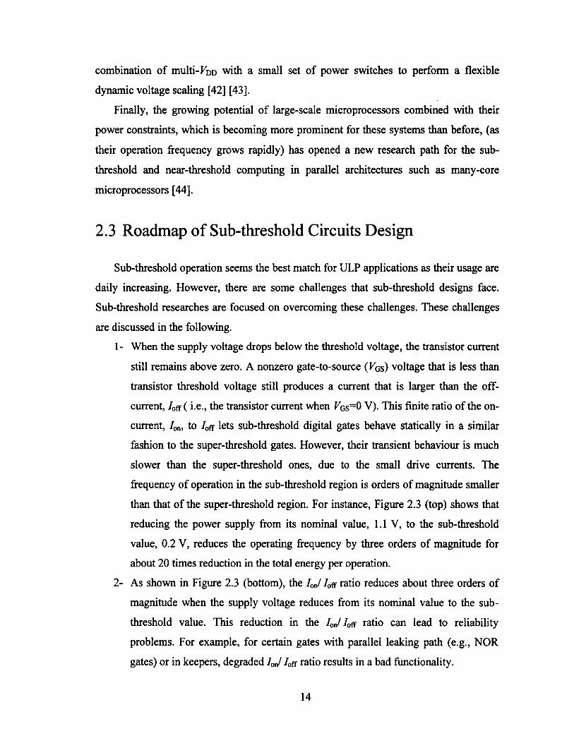
INWE: As integration density increased in CMOS digital circuits, LOCOS
technology caused problem because of the so called “bird’s beak” phenomenon, due
to the lateral oxidation. Shallow Trench Isolation (STI) with a vertical field oxide,
improves the area efficiency in device isolation. As depicted in Figure 3.3(b),
extensive gathering of the fringing field lines appears on the side of the depletion
region under the gate. This phenomenon can be modeled as an effective increase in
gate oxide capacitance [46]. According to Equation (3-8), this increase in gate oxide
with constant Qdep (AQdep ~ 0) causes a reduction in the threshold voltage as the
transistor width becomes narrower.
Therefore, we note the LOCOS cause a threshold roll-up while STI causes a
threshold roll-off as he channel width decreases.
LOCOS
A Q dev * 0
W I--
=> Qa
=>(t\
VtH‘
^ Qdep Qdep 4" A Qdep
ep T => vth T Eq. (2-8)
ireshold roll-up)
^ NWE
k W
W i
* V*=> (th
Vth
=> Cox T & A Qdep ~ 0
i Eq. (2-8)
reshold roll-off)
^N iN W Ek IV
(a) (b)
Figure 3.3 Cross-section of a MOS transistor along the width showing LOCOS (a) and STI (b) isolation and their effect on threshold voltage.
25

3.1.2.2 Effect o f Channel length
The channel length has its own effect on the threshold voltage. Two main phenomena
that the channel length impacts the threshold voltage come from the SCE and the RCSE.
SCE: In devices with long channels, the gate is completely responsible for depleting
the substrate to produce Qdep- In very short channel devices, part of the depletion is
accomplished by merging the depletion regions of the source and the drain with the
depletion region under the gate, as shown in Figure 3.4. Hence, lower is required
to deplete the substrate, i.e., decreasing the channel length decreases the threshold
voltage. This phenomenon is referred as charge sharing between the source and drain
depletion regions and the channel depletion region.
| +44-M4-H4-H
n + K 3 H ______________±Jr'
n+------------------------ ^
Depleted by- A —
Depleted by
S/D Gate
p-substrate
L i =* Charge sh arin g betw een S&.D dep le tion reg io n and Channel dep letion
^ Qdep ^ Vth ^
=> (threshold roll-off)
Figure 3.4 Charge sharing between source/drain depletion regions and the channel depletion region resulting in threshold roll-off.
Another SCE phenomenon related to the threshold voltage is drain-induced barrier
lowering (DIBL). As the drain voltage increases, the channel becomes more
attractive for the mobile charges. In other words, the potential barrier for the mobile
charges is lowered as shown in Figure 3.5 . This results in lowering the threshold
voltage lowering. As the channel length become shorter, DIBL becomes more
noticeable.
DIBL has a couple of undesirable effects that degrade the circuit performance. First,
DIBL reduces the output impedance, which is not desirable in most analog
26

applications [77]. Second, at extremely short channel lengths, DIBL causes the gate
voltage to fail in turning off the transistor completely. This means more leakage
current from the drain to source even when the transistor is in the “o ff’ state [81].
RCSE: Both “charge sharing of the source/drain depletion region and the channel
depletion region” and “DIBL” are particularly pronounced in lightly doped substrates
[46]. To mitigate these undesired phenomena, which make a threshold roll-off as the
channel length decreases, in modem CMOS technologies non-uniform p+ HALO
doping in the source-body and drain-body boundaries are used. More highly doped
substrate near the edge of the channel reduces the charge sharing effects from source
and drain depletion regions. Also, these highly doped regions at the channel edges
make the junction depletion widths smaller [8]. This reduction in the depletion
region width close to the source and drain junctions make the distance between the
source and drain longer, which leads to a reduction in the DIBL phenomenon.
Although HALO implementation supresses the charge-sharing and DIBL effects on
the threshold roll-off as the channel length decreases, it has its side effects. One of
the side effects which is related to the threshold voltage, is the threshold roll-up as
p-substrate
VDS T =» Depletion region widen near drain
Qdep in drian vicin ity T Qdep 00 su rfa ce potential
=> s u r f ace potential T
=> Voltage Barrier fo r electrons fr o m source to drian I * V th i
=» (threshold roll-off)
Figure 3.5 DIBL in a short-channel device.
27

the channel length decreases. When the channel length becomes shorter, HALO
regions in the source and drain vicinities merge together and causes an increase in
the doping level under the gate in the channel area. It means that for depleting the
surface, a larger gate voltage is needed. As the channel length becomes longer and
the distance between the HALO regions increases, the surface doping decreases
along the channel, which causes the threshold voltage reduction. The effect of HALO
doping in a short-channel device and in a long one is illustrated in Figure 3.6.
Note that the HALO is not only near the source/drain, but also it is underneath the
inversion channel. By doing this, the effect on threshold is minimal.
vysssssssssss/
HALO
Short-channel
NMOS
Long-channel
NMOS
L i => HALOs m erge => High su rfa ce doping => Qdep T => Vth T
L T => HALOs seperate => Low su rfa ce doping =» Qdep I => Vth I
1 with HALO, negligible DIBL (small Vds)
2 with HALO, noticeable DIBL (large Vds)
3 without HALO
► L
Figure 3.6 HALO doping effects on threshold voltage of short and long-channel transistors.
28

3.1.3 Capacitances
In order to understand the dynamic behaviour of MOSFETs, beside the current and
the threshold voltage, we need to study MOSFET different capacitances.
Between every two of the four terminals of an MOSFET a capacitance exists, as
illustrated in Figure 3.7. The capacitance between source and drain, however, is
negligible [15]. Figure 3.8 relates the capacitances to the geometry of an MOSFET.
D
Figure 3.7 MOSFET Capacitances.
sr®
Depletion LayerInversion
Layer
Figure 3.8 (a) Representation of MOSFET capacitances, (b) decomposition of source/drain junction capacitance to bottom and sidewall components.
29
According to Figure 3.8, the capacitances shown can be explained as below
• Ci: Oxide capacitance between the gate and the channel, expressed as
• C2: Depletion capacitance between the channel and the substrate, defined as
where Wdep is the width of depletion layer given by
w dtp = V(2<rsi0 s) / ( ? A U ) [15], 0 S is the surface potential and b is the
substrate doping.
• C 3 and C 4: Gate capacitances to source/drain due to the overlap of the gate
ploy with source/drain. Because of fringing field, these capacitances cannot
be simply written as WLDC0X. In MOSFET models, Cgdovand Cgsov represent
the overlap capacitances per unit width.
• C 5 and C(,: Junction capacitances between source/drain and the substrate. As
illustrated in Figure 3.8 (b), these capacitances are divided into the bottom
and sidewall capacitances. They depend on both the area and perimeter of the
source/drain. The area is A=WE and P=2(W+E) (Figure 3.8). The total
junction capacitance is
where Cj is the capacitance per unit area between the bottom of junction and
the substrate, Cjsw is the capacitance per unit length between the 3 sidewalls
of the junction and the substrate that are not facing the channel, and Cjswg is
the capacitance per unit length between the sidewall of the junction and the
substrate that faces the channel. All these capacitances (Cj, Cjsw, and Cjswg)
are functions of the source/drain voltages. For example, Cj may be expressed
Cx = C0XWL = WL — (3-9)
c 2 = C ^ W L = wa-^i (3-10)
C5 — C6 - CjA + CjSW(P — W ) + Cjswg W (3-11)
as [77]
(3-12)
30

where Cj0 is the junction capacitance at zero bias, is the built-in voltage,
Mj is the junction grading coefficient, and F r is the reverse voltage across the
junction. Cjsw and CjSwg can be expressed similar to (3-12), but C;0 must be
replaced by CJSW0 and Mj with MjSW or Mjswg.
Table 3.1 summarize the relation between the capacitances in Figure 3.7 and Figure 3.8.
Table 3.1 Approximation for MOSFET capacitances [80].
Figure 3.7
Capacitances
Figure 3.8
CapacitancesRelating Expression
Cdbi C<SB C5, C6 CjA+ Cjsw (W+2E)+CjswgW
Region of operation
OFF Triode Saturation
Cgs C3, C4 CgsovW Cj/2 + CgsovW 2C J3 + CgsovW
Cgd C3, c4 CgdovW Ci/2 + CgsovW CgdovW
Cgb Ci, C2 CiC2/(C! + C2) 0 0
All capacitances connected to the gate of the MOSFET should be modeled for delay
calculations. Defining CGG as the total gate capacitance, we may write
CGG — CG$ + CGp + CGg (3-13)
Due to the dependence of CGS, Cgd> and CGB to the gate voltage, CGG is also a function
of the gate voltage as depicted in Figure 3.9 [77].
Qjg
Figure 3.9 Dependence of gate capacitance of an NMOS transistor to gate voltage.

3.1.4 Leakage Currents
A static CMOS circuit consumes power even when it is in its idle mode and no
switching activities take place. The reason for this power consumption is the leakage
currents, which are not negligible in modem CMOS technologies due to the extensive
down scaling of transistors’ dimensions. There are four major sources of leakage currents
in CMOS transistors.
1. Sub-threshold Leakage (70ff)
The sub-threshold leakage current is the drain to source current of a transistor when
the transistor operates in the weak-inversion mode. The magnitude of this current can
be calculated from Equation (3-3) for Fgs=0 and F<jS= Fdd (transistor being off),
which is presented in Figure 3.2. The magnitude of this leakage current is a function
of the temperature, supply voltage, device size, and the process parameters [46].
2. Gate Oxide Tunneling Leakage (/g)
The downscaling of the oxide thickness increases the electric field across the gate
oxide resulting in electron tunneling from gate to the substrate or the source and
drain. Two mechanisms are responsible for this phenomenon: Fowler-Nordheim
tunneling and direct tunneling, where the latter is dominant at lower voltages and
thinner oxide [15]. Gate oxide leakage for NMOS transistor is higher than PMOS
transistor. Tunneling current decreases exponentially with the oxide thickness and
becomes more significant for technologies beyond 100 nm [15].
3. Reverse-biased Junctions Leakages (/sulk)
Though the p-n junctions between the source/drain to the substrate and the well to the
substrate are usually reverse biased, yet small amount of currents leak via these
junctions. The magnitude of this leakage current depends on the area of source/drain
and well diffusions and doping concentration. The highly doped shallow junctions
and HALO doping necessary to control SCE (Section 3.1.2.2) in the nanometer
devices has worsened this leakage current [46].
32

4. Gate Induced Drain Leakage (Igidl)
This leakage current is caused by high electric field in the drain junction of
MOSFETs. HALO doping in the vicinity of the drain junction, which is done to
control punch-through and DIBL in nano-scale technologies, results in band-to-band
tunnelling current at the drain edge, especially as the drain-bulk voltage increases.
Thinner oxide and higher supply voltage increases GIDL current. GIDL occurs
where the gate overlaps the drain, hence, it is a function of transistors width [15].
When a circuit operates in the sub-threshold region, voltages on the gate and the
drain are not so relatively high. This means that in the sub-threshold region of
operation the GIDL current may be neglected.
The most significant leakage current among the leakage currents is the sub-threshold
leakage current. In Chapter 4 a comparative study of the leakage currents is presented for
different technology nodes.
3.2 Quality Metrics o f a Digital Circuit
This section defines a set of basic features of a digital circuit to quantify the quality
of a design. The relative importance of these metrics depends on the application of the
circuit. For example for a desktop computer speed is a crucial property, while for a
mobile electronic device the energy consumption is the dominant metric. These
introduced properties give a good understanding for designing a digital circuit based on
special constraints.
3.2.1 Propagation Delay
The propagation delay for a logic gate is the time taken for a signal to propagate from
the input to the output node. This delay is defined as the time from when the input signal
passes Fdd/2 until the corresponding output signal passes Fdd/2, as depicted in Figure
3.10. The capacitance shown in Figure 3.10 includes the drain junction capacitance of the
first inverter and the gate capacitance for the second inverter which is acting as a load.
33
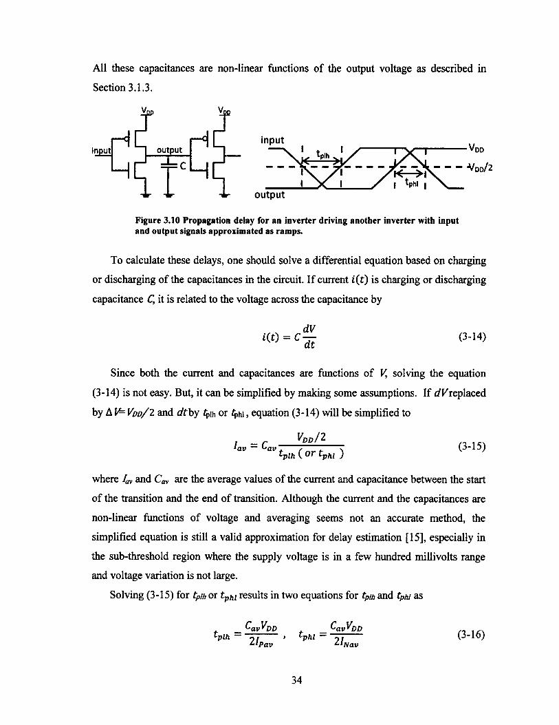
All these capacitances are non-linear functions of the output voltage as described in
Section 3.1.3.
inputH
H
outputinput
output
Figure 3.10 Propagation delay for an inverter driving another inverter with input and output signals approximated as ramps.
To calculate these delays, one should solve a differential equation based on charging
or discharging of the capacitances in the circuit. If current i(t) is charging or discharging
capacitance C, it is related to the voltage across the capacitance by
i(t) = CdV~dt
(3-14)
Since both the current and capacitances are functions of V, solving the equation
(3-14) is not easy. But, it can be simplified by making some assumptions. If ^ rep laced
by A V= Vdd/ 2 and d tby ^ih or tj>hi, equation (3-14) will be simplified to
VddI2I = Cl av u a i? . (3-15)
tpih ( or tphl )
where 4v and Cm are the average values of the current and capacitance between the start
of the transition and the end of transition. Although the current and the capacitances are
non-linear functions of voltage and averaging seems not an accurate method, the
simplified equation is still a valid approximation for delay estimation [15], especially in
the sub-threshold region where the supply voltage is in a few hundred millivolts range
and voltage variation is not large.
Solving (3-15) for tpih or tpM results in two equations for tpih and tPhi as
tpih ~a v y DD
21Pavlphl
^av^DDNav
(3-16)
34

where IPav and INav are the PMOS and NMOS transistors average currents, respectively.
The propagation delay tp is defined as the average of the two factor:
tpih T tphl _ Cqv(3-17)
2 ■^Nav I p a v '
To optimize the propagation delay, according to Equation (3-17), the effect of transistor
sizing should be considered on C/7 ratio. A detailed study on the delay optimization is
presented in Chapter 5.
3.2.2 Power Consumption
Power dissipation in a CMOS circuit has two components: dynamic and static
dissipation.
Dynamic power arises from
• Switching power consumption that refers to the power consumption due to
the charging and discharging of a capacitance, C, and expressed as
where f is operation switching frequency and a is the switching activity
factor. The switching activity factor is the probability that a node makes a
transition from 0 to 1. Only in this transition a node consumes the power
extracted from the voltage supply.
• “Short-circuit” current power consumption while both pull-down and pull-up
transistors are partially ON, and may be written as
where lsc- av is the average short-circuit current. It is important to keep the
signal edges fall and rise fast to have negligible Psc-
Putting these two together gives the total dynamic power consumption of a circuit
Psw — aCV£D f (3-18)
(3-19)
35

PDYN ~ gCVpp / + Isc -a y V p D
Psw Psc(3-20)
The dynamic power consumption mostly consists mostly of the switching power and
the short-circuit power dissipation is normally less than 10% of the whole [15]. Hence, as
Pfohas a quadratic relation to PDYn , it is important to select the minimum Vdd that meets
the required frequency of operation.
The static power consumption is caused by leakage currents and may be expressed as
where all leakage currents are described in Section 3.1.4.
3.2.3 Energy Consumption
In an inverter when the output makes a transition from 0-> Vd d , the dynamic energy
drawn from the power supply in one cycle is
This means that during this transition, 50% of the total energy drawn from the supply
is consumed by the PMOS transistor. For the output transition Vdd 0, the stored energy
power supply.
The other component of the consumed energy is the static or leakage energy in one
cycle, which may be expressed as
where tp is the propagation delay or the needed time to complete one computation and
Iuak is the total leakage current.
PsT ~ ( j o f f + fc + lB u lk )V DD (3-21)
(3-22)
For this transition, the stored energy in the load capacitance is
E = (3-23)
in the capacitor is consumed by the NMOS transistor and no energy is drawn from the
E s t ~ I Leak Vd d tp (3-24)
36

Substituting tp from Equation (3-17) to Equation (3-24), the leakage consumed
energy becomes
Est — heakVDD T7 Li.o n -a v(3-25)
Putting Equations (3-22) and (3-25) together, the total energy consumption comes to
Equation (3-26) shows a quadratic relation between the total consumed energy and
the supply voltage. Hence, decreasing Vdd decreases the total energy quadratically.
However, decreasing Vdd decreases I0n-av t0°- 1° the other words, decreasing VDd
increases E jr while decreases EDYn- So , it is predictable that the consumed energy shows a
minimum point with respect to Vdd as shown in Figure 3.11. In [1] and [36], the authors
show that the minimum energy point occurs at a Vdd in the sub-threshold or near
threshold region.
The minimum energy point typically consumes an order of magnitude less energy
than the conventional operation point; however it operate at least 1000 times slower [15].
Accordingly, there is a trade-off between the optimum propagation delay and the
Leak(3-26)
Minimum Energy Point
Energy '
ElEt
Vdd
Figure 3.11 Minimum energy point
37
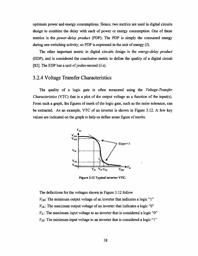
optimum power and energy consumptions. Hence, two metrics are used in digital circuits
design to combine the delay with each of power or energy consumption. One of these
metrics is the power-delay product (PDP). The PDP is simply the consumed energy
during one switching activity; so PDP is expressed in the unit of energy (J).
The other important metric in digital circuits design is the energy-delay product
(EDP), and is considered the conclusive metric to define the quality of a digital circuit
[82]. The EDP has a unit of joules-second (J.s).
3.2.4 Voltage Transfer Characteristics
The quality of a logic gate is often measured using the Voltage-Transfer
Characteristics (VTC) that is a plot of the output voltage as a function of the input(s).
From such a graph, the figures of merit of the logic gate, such as the noise tolerance, can
be extracted. As an example, VTC of an inverter is shown in Figure 3.12. A few key
values are indicated on the graph to help us define some figure of merits.
The definitions for the voltages shown in Figure 3.12 follow
Voh: The minimum output voltage of an inverter that indicates a logic “1”
Voi'- The maximum output voltage of an inverter that indicates a logic “0”
Fil: The maximum input voltage to an inverter that is considered a logic “0”
Fh: The minimum input voltage to an inverter that is considered a logic “1”
Vil VIH Vdd ”
Figure 3.12 Typical inverter VTC.
38

From the VTC, one can see that if Fi„<ViL, the output voltage is a valid logic 1, and,
similarly, if Fin>ViH, the output voltage is a valid logic 0.
When cascading inverters, we can define the noise margin high, NMH that ensures a
logic “1” output from the first inverter is interpreted as a logic “1” input for the second
inverter. Similarly, we can define the noise margins low, NML that ensures a logic “0”
output from the first inverter is interpreted as a logic “0” input for the second inverter.
The expressions for these noise margins are given by
NMH = V0H - VIH(3-27)
NML = VIL - V0L
Static Noise Margin (SNM) is defined as the minimum of the two noise margins
expressed in Equation (3-27).
3.3 Chapter Summery
In this chapter we reviewed most of the material that we need in the following
chapters to study the effect of transistor sizing either on the transistor’s behaviour by
itself or digital circuits’ optimization.
In Chapter 4, the effect of transistor sizing on MOSFET characteristics in the sub
threshold region, such as the threshold voltage, current, and capacitances are studied in
detail for different available CMOS technology kits. Based on what discussed in Chapter
4, in Chapter 5 a method for delay optimization is presented.
39

4 MOSFET Behavior in Sub-threshold Region
To have a better understanding of transistor-sizing effects on a digital circuit
performance and its power consumption in the sub-threshold region, the behavior of a
transistor must be studied individually in this region of operation. The main important
characteristics of a transistor that should be studied are: threshold voltage, transistor ON
and OFF (leakage) currents, capacitances, and sub-threshold slope. In this chapter the
effect of the channel length and width on these parameters are studied. The studied
CMOS technology nodes are: TSMC 180nm, IBM 130nm, TSMC 90nm, and TSMC
65nm LP. In the TSMC 65 nm technology node, two flavors of transistors are provided:
low-threshold (lvt) and standard-threshold (svt). In each technology node an investigation
has been done on the NMOS and PMOS transistors.
4.1 Threshold Voltage Variation
Due to the exponential relation between the sub-threshold current and the threshold
voltage, as shown in Equation (3-3), a small change in the threshold voltage causes a
significant change in the sub-threshold current. Hence, any changes on threshold voltage
caused by the transistor dimensions must be considered to predict the behavior of the
current in this mode of operation.
As explained in Section 3.1.2, in older technologies, where LOCOS is used for
transistors isolation and HALO doping is not used, a roll-up and roll-off of the threshold
voltage has been seen with the channel width and channel length reduction, respectively.
On the contrary, in the modem technologies, which LOCOS is replaced with STI and
HALO doping is used to mitigate the DIBL and punch through in very short channel
devices, a roll-off and roll-up of the threshold voltage is seen for a decrease in the
channel width and length, correspondingly. Figure 4.1 shows the threshold voltage
dependence on the channel length and channel width for the NMOS and PMOS
40

transistors in IBM 130 nm CMOS technology. The left plot shows the INWE, while the
right plot represents RSCE.
0.45
0.44
0.43
0.42
0.41
0.39
0.38
0.37
0.36
0.35250 500 750 10000
0.5
0.45 thn
0.4
0.35
0.3
0.25
0.2 -
0.15
0.1250 500 750 1000
L (nm)
Figure 4.1 Threshold voltage versus the channel width at Lmitt =120 nm(left), and threshold voltage versus the channel length at Ff'min=160 nm (right) for IBM 130 nm technology.
Figure 4.2 and Figure 4.3 show the PMOS and NMOS transistors’ threshold voltage
variation with respect to the channel width in different technology nodes, respectively. As
it is appearing in Figure 4.2, INWE is not significant for PMOS transistors in the 65 nm
technology. It means that for 65 nm PMOS transistors, the sub-threshold current shows a
nearly linear relation to W, as shown in Figure 4.9 (d,e) of Section 4.2.
Figure 4.4 and Figure 4.5 show variation of the threshold voltage with respect to the
channel length for the PMOS and NMOS transistors, respectively. Due to the RCSE, the
threshold voltages show roll-up as the channel length decreases in all considered
technologies.
41

0.65
0.6
0.55
0.5
0.45
0.4
0.35
0.3
0.25
m s m
* * * * *
ummiumuiiuuummmunH-
"O 180 nm$ 130 nm• 90 nm+ 65 nm (Ivt) 0 65 nm (svt)
0 200 400 600 800 1000 1200 1400W( nm)
Figure 4.2 Threshold voltage versus W at KDD=0.2 V for a PMOS transistor in different technology nodes at L=Lmin
IWmumiixiiiiii
Figure 4.3 Threshold voltage versus W at FDD=0.2 V for an NMOS transistor in different technology nodes at L=Lmin
42
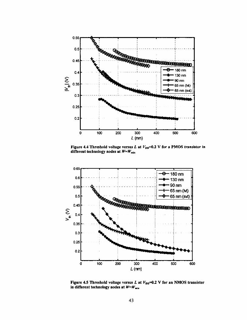
0.55
0.5
0.45
180 nm 130 nm 90 nm 65 nm (Ivt) 65 nm (svt)
0.4s— 0.35
0.3
0.25
0.2
0 100 200 300 400 500 600L (nm)
Figure 4.4 Threshold voltage versus L at FDD=0.2 V for a PMOS transistor in different technology nodes at W=Wmin
0.65180 nm 130 nm 90 nm 65 nm (Ivt) 65 nm (svt)
0.6
0.55
0.5
0.45
0.4£0.35
0.3
0.25
0.2
0 100 200 300 400 500 600L (nm)
Figure 4.5 Threshold voltage versus L at FDD=0.2 V for an NMOS transistor in different technology nodes at W=Wmin
43

4.2 Current Behaviour
According to the super-threshold current Equation (3-1), due to the nearly linear relation
between the current and the threshold voltage, a small change in the threshold voltage
does not show significant any influence on the current. Therefore, the current is a nearly
linear ascending function of W and a descending function of L as depicted in Figure 4.6.
20400
■ 18360
320 Current vs. L Current vs. W
280
£ 240<3 200c<De 160=3o
120
80
40
0 200 400 600 800 1000 1200 1400 1600 1800 2000
<0><zS.cgZJo
W(nm) at L^n L(nm) at
Figure 4.6 Super-threshold current for a PMOS transistor at VDB=l V versus L and W, in IBM 130nm CMOS (NMOS transistor shows the same behavior).
However, in the sub-threshold region, because of the exponential dependence of the
current to the threshold voltage, the behavior of the current is not as simple as the super-Vththreshold current. Quoting Equation (2-3), factors W /L and exp(-—^— ) do not show the
same behavior (with respect to each other) as the transistor dimensions change.
For instance, when L increases (decreases), V,h decreases (increases) as shown inVrs—VthFigure 4.4 and Figure 4.5. Thus, ML decreases (increases) while exp (—■ ) increasesYlV7*
44

(decreases). Since the sub-threshold current is proportional to the multiplication of these
two last factors, the current shows an unpredictable behavior with respect to the channel
length variations. Depending on which factor changes more, the current tracks its
behavior. For example, if we double the channel length, W/L will be halved, while the
amount of change in exp is unknown. Suppose that exp ( ™ ^ iL) becomes
doubled. Hence, the multiplication of these two factors does not change; i.e., no changeVthin the current occurs. However, if exp(-- ~ - ■ ■) increases more (less) than twice, the
current shows an increase (decrease). Thus, the current could be an ascending or a
descending function of L and the same discussion is valid for W.
In Figure 4.7 the two factors are plotted in the top figure for a PMOS-lvt transistor in
the TSMC 65 nm LP CMOS technology. It is depicted that these two factors vary in
opposite directions with respect to the channel length. Multiplication of these two factors
1001ex p o n en tia l factor 1/L factor
0.5 c
1 0.25
050 100 150 200 250 300 350 400
e 2.60'■£ 2.41 2.2 .0 Q O O O
1.3 = 1.2 §current
tw o factors m ultiplication1.41.2
c250 300 350 40050 100 150 200
L (nm)
Figure 4.7 Top figure shows normalized 1/L and e x p ( ^ ^ ~ ) factors individually
plotted versus L. The bottom figure shows normalized 1/L X exP ( ~ ^ ~ ) and
normalized current at Kdd=0.2 V for TSMC 65 nm LP CMOS kit for a PMOS-lvt transistor a t W=Wmin=120 nm.
45

is plotted in the bottom figure. It shows a peak at the same point, where the actual current
shows its maximum point.
Figure 4.8 shows l/L and exp factors for a PMOS-svt in the TSMC 65 nm
LP CMOS (top figure). Although the exponential factor shows an incremental behaviour
with respect to L, like what occurs for a PMOS-lvt, the multiplication of these two factors
does not show any maximum value contrary to what occurs for a PMOS-lvt. This fact
shows that despite of ascending behaviours of the exponential factor with respect to L in
( Vns—Vth \— J, which replicates the sub
threshold current, might have different behaviours versus L.
exponential factor 1/L factor
T“0.5
T J<DNIOc
100 150 200 250 300 350 400
%TJ *2 (D - .tij (OE a> £ c
xa>
•5 0.8
co*3 (O oCL'JPZ3ETJ<uN75
oc
0.6
0.4
current' two A ctors multiplication
0 (^0 0 0 0 0 0 0 0 ^ )50 100 150 200 250
L (nm)300 350
■ 0.8
cg3
T J(UN■ 0.6
400
Figure 4.8 Top figure shows normalized l/L and exp(- --^y- ) factors individually
plotted versus L. The bottom figure shows normalized 1 ILK e x and
normalized current at Fdd=0.2 V for TSMC 65 nm LP CMOS kit for a PMOS-svt transistor at W=W™t*=120 nm.
oc0.4
46

The current behavior in the sub-threshold region with respect to W and L not only
varies from one technology node to another technology node, but also varies from one
transistor type to another transistor type in the same technology node. Moreover, in some
technology nodes where different flavours of transistors are provided, for example Ivt and
svt in the TSMC 65 nm LP CMOS, the same type transistors might show different
behavior.
As a summary, the sub-threshold current versus W and L are shown in Figure 4.9 and
Figure 4.10, respectively. As it is appearing in these figures, and consistent with what
discussed before, the current behaviour is not the same for all technologies.
<c
1000
750
500ct:3 250 O
0
90nm(c)
65nm (Ivt transistors)(d)
100
' 75 .... .................... ; i
50 k ■ -- ---- 1
25
0
k ■ - • • -
500 1000 1500 2000 2500 3000
65nm LP (svt transistors)(e)
200 400 600 800 1000W(nm)
6<c'W4c<Dt 23o
00 200 400 600 800 1000
W{m)
Figure 4.9 Sub-threshold current versus W in different technology nodes at Fdd=0.2 V and JLmin.
47

Figure 4.11 shows that in the 130 nm, 90 nm, and 65 nm (Ivt) technology kits, both
NMOS and PMOS transistors show a peak value versus L (Figure 4.11 (b,c,d)), while in
the 180 nm only the PMOS transistor has a maximum point versus L (Figure 4.11(a)).
I80nm(a)
0.09
0.085
0.08
0.075
0.07
Q. 0.065
0.06500100 200 300 400
90nm(c)
65nm LP (svt transistors) (e)
180
170
,180
8 20130
120100 200 300 400 500
0.6
% 0.5
R 0.4
2 0.3
0.2500100 200 300
L(nm)400 600
oCO
. o
130nm(b)
150
1254.5
100
0l 2.5
1500500 1000
65nm LP (M transistors)(d)
■NMOS■PMOS
COo
3.5
i3oCOosQ. 12.5
300 400L( nm)
500 600100 200
Figure 4.10 Sub-threshold current versus L in different technology nodes at Fdd=0.2 V and Wmin.
One should notice that the maximum point for the sub-threshold current versus the
channel length depends on the supply voltage. As the supply voltage increases, the
maximum point for the current becomes closer to the minimum length. Figure 4.11 shows
that in the 130nm technology for larger supply voltages, the maximum point for the
current occurs in smaller lengths. This also happens in the other technologies. Figure 4.12
shows the channel length where the sub-threshold current becomes maximum, Zimax,
versus the supply voltage for different CMOS technologies. As the supply voltages reach
48

the super-threshold region, Zimax moves to the minimum length. In different technologies
this happens in different supply voltages. According to Figure 4.4 and Figure 4.5, the
threshold voltage in the 90 nm technology is the smallest threshold voltage among the
four considered technologies. Hence, it is predictable that Zimax for the 90 nm becomes
the minimum channel length in smaller supply voltages, which is verified in Figure 4.12.
400
350
300
250
I 200 ,=840 nmImax150
100,=980 nm’bmx
200 400 600 800 1000 1200 1400 1600 1800L (nm)
Figure 4.11 Sub-threshold current versus the channel length for an NMOS transistor in IBM 130 nm technology at Wmi„. The maximum point becomes smaller as the supply voltage increases.
4.3 MOSFET Capacitances
Another important element that should be studied for the delay and energy
optimization is the transistor capacitances. As discussed in Section 3.1.3, there are several
different types of capacitances between the transistors terminals. In that section we just
introduced the general concept, but in this section we will study the behaviour of all
capacitances in more detail with respect to the transistor dimensions and its terminal
voltages.
49

180nm
260| 240
220200
0.1 0.2 0.3 0.4 0.5 0.6vk>M90nm
250E*c
1- j
200
150
1000.1 0.15 0.2 0.25 0.3 0.35 0.4
130nm1200j
1000
800£c
i-j600400200
0.50.1 0.2 0.3 0.4 0.6voo<v>
65nm (M transistors)350NMOSPMOS300
Ec 200J 150
1000.2 0.3 0.4 0.5 0.60.1
voo<v>
Figure 4.12 versus VDD at Wmia.
Voltage dependence of MOSFET capacitances
As explained in Section 3.1.3, the gate capacitance of a MOSFET is a combination of
the gate oxide capacitance, fringing capacitance due to the gate overlap to source and
drain, and depletion capacitance under the gate area. Among all these mentioned
capacitances, only the first portion of the gate capacitance is independent of the gate
voltage, but the rest are non-linear functions of the gate voltage. For example, Figure 4.13
shows the dependence of the gate capacitances to the gate voltage. Simulations are
performed for the NMOS transistor in the IBM 130 nm technology for two different
values of F d s - In small F ds where the channel is uniform, C gd and Cos change in the
same manner. At higher Fds where the channel is narrower near the drain, Cos is bigger
than Cgd- The capacitance Cgg is Cgd+ Cgs+ Cgb and is almost independent of Fds, but
is a nonlinear function of the gate voltage. In delay optimization, to have a more accurate
result, one should take this behaviour into account.
There are two other capacitances that are involved in the delay and energy calculation
and optimization. These capacitances are the capacitances between the source and drain
junctions and the body due to the reverse- biased diodes at these junctions. As evident
50

'GD250'GS
'GB
200 'GG
150
100
250
200
(08 150 c8oQ.8 100
<00
Figure 4.13 Gate capacitances versus gate voltage for an NMOS transistor in IBM 130 nm for two different FDS. CGG is equal to the sum of the other three capacitances.
from Equation (3-12), these capacitances are non-linear functions of the reverse-bias
voltages applied to these junctions. If the source and body are connected together, like the
case of an inverter, only Cdb affects the delay and energy. In Figure 4.14 the drain-body
capacitances for an NMOS transistor in IBM 130 nm technology is plotted as an
example. It shows the non-linear relation of this capacitance to Fps and also shows its
independence of Fgs- In other technologies the same behaviour is seen, but here only the
results of the IBM 130 nm are reported.
Size dependence of MOSFET capacitances
The capacitances of a MOSFET are related to both the channel length and width,
except for the two junction capacitances that are only related to the channel width. In this
section we will study the effect o f the channel length and width only on C qo and C db in
the sub-threshold region. As depicted in Figure 4.15, both capacitances are linear
function of the channel width. However, the gate capacitance is not a linear function of
the channel length near the minimum channel length. The drain junction capacitance
51
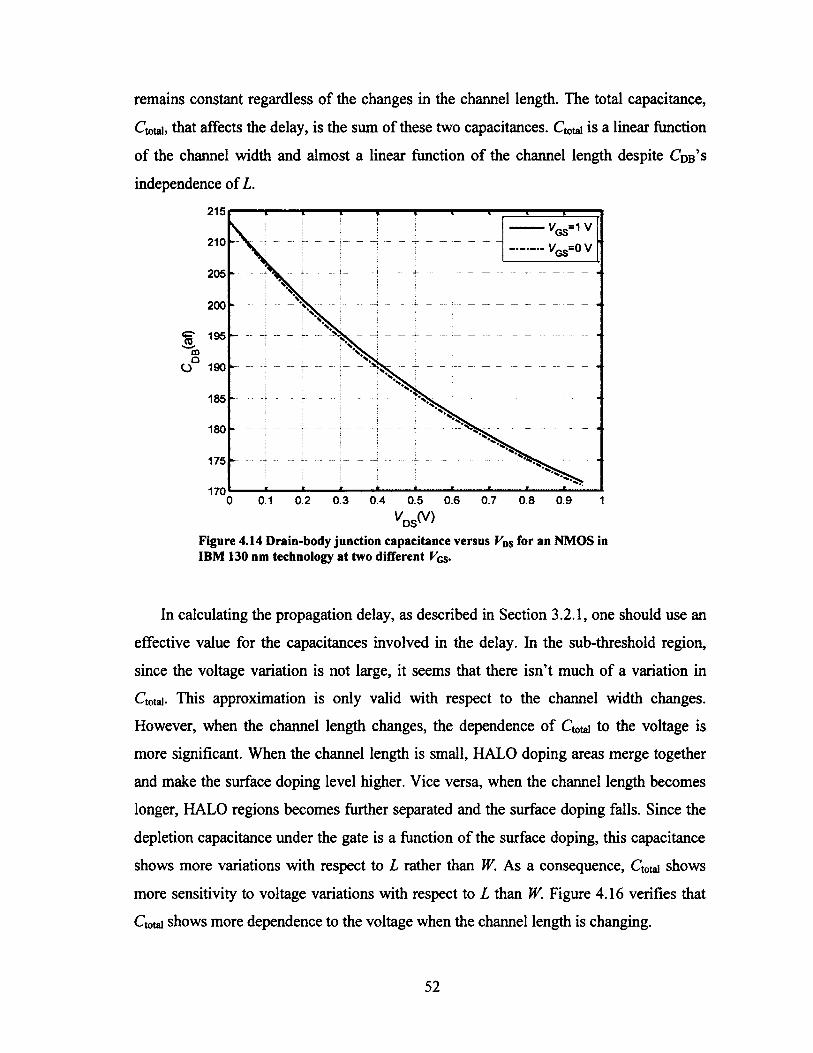
remains constant regardless of the changes in the channel length. The total capacitance,
Ctotai, that affects the delay, is the sum of these two capacitances. C totai is a linear function
of the channel width and almost a linear function of the channel length despite C d b ’s
independence of L.
215
210
205
200
I 195""moO 190
185
180
175
170 0.1 0.2 0.3 0.4 0.5 0.6 0.7 0.8 0.9
Figure 4.14 Drain-body junction capacitance versus Fds for an NMOS in IBM 130 nm technology at two different PGS.
In calculating the propagation delay, as described in Section 3.2.1, one should use an
effective value for the capacitances involved in the delay. In the sub-threshold region,
since the voltage variation is not large, it seems that there isn’t much of a variation in
Ctotai- This approximation is only valid with respect to the channel width changes.
However, when the channel length changes, the dependence of C totai to the voltage is
more significant. When the channel length is small, HALO doping areas merge together
and make the surface doping level higher. Vice versa, when the channel length becomes
longer, HALO regions becomes further separated and the surface doping falls. Since the
depletion capacitance under the gate is a function of the surface doping, this capacitance
shows more variations with respect to L rather than W. As a consequence, C totai shows
more sensitivity to voltage variations with respect to L than W. Figure 4.16 verifies that
C totai shows more dependence to the voltage when the channel length is changing.
52

tota
l
<W'COQ*(T»1200
1000
1400
0001200
oS. 000
000400
000200
400
200 200 400 000 000 1000WM.ti*, t(nm)
200 400 000 000 1000
Figure 4.15 Gate and drain capacitances versus the channel width and channel length for an NMOS in IBM 130 nm at FDS=FGS=0.2 V.
18001400
v'd s“ ° - 1̂ g s ‘°-2VW°-2.V °-1
V„-0.1,VQS«0.21600
1200
1400
10001200
om800
800600
600
400400
200 200200 400 600 800 1000 200 400 600 800 1000L (nm)
Figure 4.16 C,otl| versus the channel length (left) and versus the channel width (right) for an NMOS in IBM 130 nm for two sets of voltages that are used in delay modeling and estimation.
53

4.4 Leakage Currents
Understanding the leakage currents’ behaviour is the main key to optimize the energy
consumption, especially in the sub-threshold region where the relative contribution of
the leakage energy is more than the case of the super-threshold region. In this section we
will study the effect of transistor sizing on three main components of the leakage current:
the gate leakage (7g), the sub-threshold leakage (70ff), and the source/drain junctions’
leakage (hu\k)- The general concepts of these leakage currents were presented in Section
3.1.4. To measure the leakage currents, the simulation test benches are arranged as shown
in Figure 4.17.
The simulation measurement results for the two types transistor are shown in Table
4.1. As can be seen in this table, the sub-threshold leakage, 70fr, has the biggest portion
among the leakage currents elements. This element of leakage current is about three
orders of magnitude larger than the two other leakage elements. Changing the transistor
dimensions doesn’t lead to a significant change on this percentage and 70fr remains as the
dominant leakage element regardless of the transistor dimensions. Therefore, in the
following discussion our main focus is on 70fr as the main leakage current component.
In the sub-threshold region of operation both 7on and 70fr are expressed by
Equation (3-3) except that to calculate 70ff, the gate-source voltage Fgs is set to “0”.
Hence, it seems that the “off’ and “on” currents show the same behaviour with respect to
the changes in the transistor size. For instance, in Figure 4.18 the “o ff’ and “on” currents
for a PMOS transistor in IBM 130 nm are illustrated at Fdd=0.2 V. As seen in the graphs,
/0ff and Ion have very similar changes with respect to the channel length and width
variations. A minor difference can be noticed when the channel length is changing. This
difference is due to the dependence of the charge carries mobility (ji) and the sub
threshold slope factor («) to the gate-source voltage1. These dependences to Fqs are more
noticeable for the channel length variation than the channel width variation. Although not
reported here, we found the same trend to be true for other technologies.
1 KGs affects n due to the mobility degradation [15] and affects n due to the induced changes in the depletion region under the gate.
54

Table 4.1 The leakage currents for NMOS and PMOS transistors in each technology at their minimum acceptable sizes.
180nm NMOS
Super-threshold^DD=1
Sub-thresholdFdd=0.2
/o ff
Super-thresholdYdd=1
5 5 2 f
Sub-thresholdkj>D=®*2
1 5 .3 2 p
/(Sulk
Super-thresholdFdd=1
5 .7 6 a
Sub-thresholdFdd=0.2
5 .7 6 aPMOS 2 6 .4 8 p 1 7 2 .2 f 4 .7 5 a 4 .7 5 a
130nm NMOS 4 .1 4 f 7 0 .5 7 a 2 1 7 .3 p 5 9 .6 1 p 6 3 9 a 1 5 6 zPMOS 8 1 9 a 1 8 .4 5 a 3 9 .4 7 p 1 4 .5 3 p 2.1 a 6 4 .3 9 z
90nm NMOS 3 0 .6 p 8 1 0 f 2 .9 6 6 n 9 5 2 p 9 .6 7 f 1 .9 7 aPMOS 1 2 .1 1 p 4 8 6 f 2 1 7 .4 p 6 4 .1 9 p 4 4 .8 a 8 3 8 z
ONtit Iv tNMOS 4 6 9 f 8 .6 2 f 2 0 1 p 2 5 .9 8 p 3 8 9 a 3 2 0 z
PMOS 2 1 8 f 5 .5 8 f 53 p 7 .4 6 p 9 2 a 1 9 5 z
s v tNMOS 1 3 7 f 3 .4 1 2 f 1 6 .0 6 p 4 .1 6 2 p 4 9 a 3 4 8 zPMOS 163 f 3 .4 f 8 .8 6 5 p 2 .2 3 p 8 8 a 2 2 7 z
NMOS
X
?VDDIg
B
D /p ffl D D
PMOS -Yqd
Ig
JL-J TB
T D "j'pp “^1n s
BD
/Bulk
Figure 4.17 Test benches used for leakage currents measurement
55

15 100
on
14.5
14 • 4
10 & c o
13 « 3
12.5
12 200 400 600 800 1000L( nm)
200 400 600 800 1000l'V(nm)
Figure 4.18 / ofr and /,„ versus L (@ lFmill) left figure, and versus W (@ Lmm) right figure for PMOS transistor in IBM 130 nm technology at FDD=0.2 V.
Instead, we report an important figure of merit in CMOS digital circuits operating in
the sub-threshold region, the 7on / 10« ratio. The higher 7on / 10« ratio means more
robustness and immunity to noise. In designing sub-threshold SRAM, read and hold
stability, and write ability, are strongly related to 70n/70ff [9]. Besides to robust sub
threshold circuits design, 70n / 7off ratio is an important factor in optimizing the leakage
energy (Equation (3-26)) that has a large share in the total energy consumption in the
sub-threshold region. 70n/70ff is sketched in Figure 4.19 for each of four considered
technologies. This figure shows that changing the channel length has more benefit in
improving 7on / hn ratio than increasing the channel width, except for the PMOS
transistor in the 180 nm technology.
56

on off
on
off
on off
on
off
PMOS 180nm NMOS 180nm400
•g 350
300 oooooooDPQoee250
500 1000 1500
400
300
200
100500 1000 1500
PMOS 130nm NMOS130nm1000
«=o500co
400
300
200
100
PMOS 90nm NMOS 90nm250
lt=o200c
o
150500 1000 1500
400
300
200
100500 1000 1500
PMOS-lvt 65nm NMOS-M 65nm600
400
200
800 1000l/V|nm)at L .
' ' min/.(nm) at W
400
5 350
o 300
250800 1000
min
vs. Won offon off
W nm)atL .' ' min
L(nm)atW .' ' min
Figure 4 .19/on/ / offversusL and versus W (@Lmm) at FDD=0.2.
57

4.5 Sub-threshold Slope
The sub-threshold slope, S, is an important factor in designing a CMOS digital circuit
operating in the sub-threshold region. The parameter S typically varies in the range Of 70
tolOO mV/dB for the available CMOS technologies. A smaller S for a transistor implies
that the transistor can do faster transition between the “o ff’ and “on” states, which means
higher speed and less short-circuit energy consumption. Since S is related to the depletion
capacitance under the gate area, as expressed in Equation (3-7), it seems that transistor
sizing will affect this parameter.
In this section we study the effects of the channel dimensions on this parameter.
Figure 4.20 shows the variation of S with respect to W and L. As it shows, increasing L to
several folds of the minimum channel lengths, decreases S which is more desirable for
designing the sub-threshold digital circuits. However, increasing W in some cases
increases S or slightly decreases it, except for the NMOS transistor in the 130 nm and the
PMOS transistor in the 180 nm.n m o s n m o s
180 ran 130 ran
80
CO 76
72 200 400 600 800 1000 1200
85
80
75
70
65
600 200 400 600 800 1000
P M Q S p M 0 S105
100
200 400 600W'nm)
800 1000 1200
105
100
90
200 400 600 800 1000L(nm)
Figure 4.20 Sub-threshold slope versus W (@ Lmi„) (left) and versus L (@ JFmin)(right) for NMOS and PMOS transistors.
58

4.6 Chapter Summary
In this chapter we studied the effects of transistor sizing on the threshold voltage of a
MOSFET. Due to the exponential relationship between the sub-threshold current and the
threshold voltage in the sub-threshold region, the current behavior in this mode of
operation is not like the super-threshold current. In the super-threshold region the current
has its maximum when the channel length is in its minimum value. This means that in the
super-threshold operation the channel length is usually fixed to its minimum values,
except in some special applications.2 However, the sub-threshold current shows a
maximum point when the channel length is larger than minimum in most cases. This fact
implies that in the sub-threshold operation for digital applications the channel length can
be increased to maximize the deriving current.
Besides increasing the current driveability, increasing the channel length improves /on
//off ratio. The higher Ion //0ff ratio makes digital circuits operating in the sub-threshold
region more reliable and more noise immune. Also, the leakage energy is related to /on//off
ratio inversely; i,e., higher /on //0ff ratio means less leakage energy consumption.
Another benefit of increasing the channel length is obtaining a smaller sub-threshold
slope. The smaller S makes a faster transition from the “on” state to “o ff’ state and vice
versa, which means faster circuits and less short-circuit power consumption.
In the next chapter the effect of the channel length on the delay optimization is
presented. A method to find the optimum channel length is proposed. A simple inverter
RO is studied to verify the effectiveness of the proposed method. Then, the other
transistor connections (serial and parallel) are studied to find the optimum channel for
NAND and NOR gates.
2 Current-mirrors with high output impedance in analog applications, and keepers in PTL logic gates in digital applications.
59

5 Delay Optimization in Sub-threshold Circuits
Digital and analog circuits operating in the sub-threshold mode are widely used for
ultra-low-power applications, e.g., biomedical devices. The current in the sub-threshold is
typically 1000 times smaller than that of the super-threshold current. The main drawback
of the sub-threshold circuits is their low speed (typically in the range Of 1 -10MHz) due to
their small drive current. In some applications where the speed is not the main concern,
this range of speed seems adequate. However, in some applications like mobile wireless
devices, where both speed and energy consumption are important for designers, using the
sub-threshold mode without improving the operation speed is impossible. There are a
number of reports on speeding up sub-threshold circuits by manipulating the channel
width and fingering wide transistors to narrower transistors [52] [53] [54] [55] [56] [73].
Here in this chapter we are proposing our own method based on the channel length
manipulation. Increasing I up to a few times of the minimum length (e.g., 2-3 times),
causes a noticeable improvement in the performance of CMOS circuits operating in the
sub-threshold region. Depending on the technology node, and the transistor type, and the
supply voltage, the channel length where the performance becomes optimum changes. In
the following sections we proposed a method for finding the optimum channel length and
then verify it with some sample circuits. Throughout the work presented in this chapter,
the channel width is fixed to its minimum value unless otherwise mentioned.
5.1 Current-over-Capacitance (CoC)
According to Equation (3-16), the propagation delay is proportional to Cl I ratio,
where C is the total capacitance connected to the node and / is the driving current that
charges or discharges C. In our proposed method we made an assumption that each
transistor operates independently. In the high-to-low transitions we ignored the effects of
the PMOS transistors and in the low-to-high transitions we ignored the effects of NMOS
transistors. In other words, we optimize /pih and /Phi individually and find the optimum
60

channel length for each of NMOS and PMOS transistors individually. Although initially
this method might seem inaccurate, it is a quick and still reliable solution. It spares the
need for exhaustive blind simulations that are very time consuming, especially in large
circuits with millions of transistors. Consider the case that an inverter is driving an
identical one, as shown in Figure 5.1. The capacitances that are involved in the
propagation delay are the drain junction capacitances of the first stage ( C d b n i , C d b p i) and
the gate capacitances of the next stage (C g g n 2 , C ggp2)- A s shown in this figure in the
high-to-low transition N1 discharges the total capacitance C and in the low-to-high
transition PI charges it. Therefore, we may rewrite Equation (3-16) as
assuming C d b n i= C d b p i= C db and C g gn2=Cggp2= C gg ,that are valid approximation for all
considered technologies, Equation (5-1) can be summarized as
To minimize the propagation delay, Equation (5-2) implies that the Current-over-
Capacitance (CoC) ratio should be maximized. As explained in Section 4.2, the sub
threshold current shows a maximum point as the channel length increases except for the
NMOS transistor in the 180 nm technology and for the 65 nm technology for the svt
flavour of transistors. Hence, it is acceptable to look for a channel length where CoC
becomes maximum (IcoCmax)- Also it is predictable that Z-coCmax will be smaller than Ljmax
introduced in Section 4.2. To find ZcoCmax for each type of transistor in each of the four
technologies, we biased an NMOS and a PMOS transistor with DC supplies; then
measured the drain current and C qg and C db to find the CoC ratio.
As discussed in Section 4.3, both C gg and C db are voltage dependant. Since
propagation delay is defined as the time from when the input signal passes V\xJ2 until the
(Q jb jv i + C d b p i + CGGN2 + CGGP2)V DD
avP 1
(5-1)
tphi ~(C pB N l + CDBp i + CGGN 2 + CGGP2)V DD
21avN l
avN 1
(CpB + CGG)VDD(5-2)
61
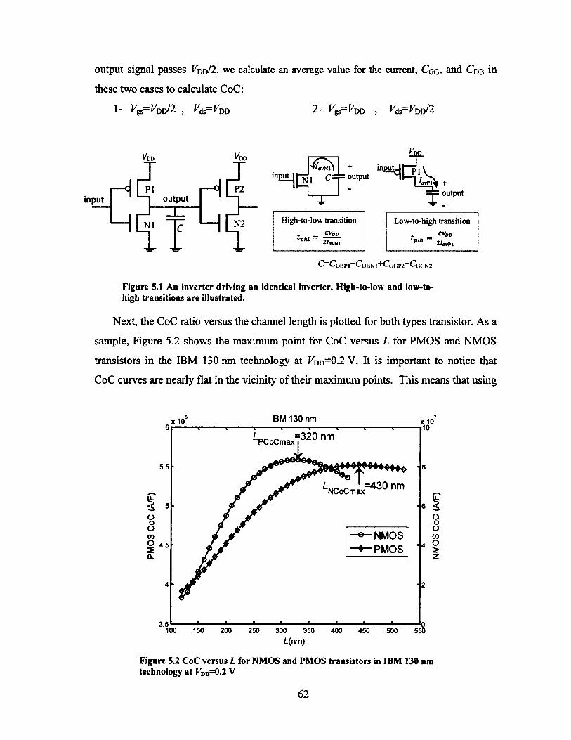
output signal passes Fdd/2, we calculate an average value for the current, Cqq, and Cdb in
these two cases to calculate CoC:
2- Fgs=FDD , FdS= Fdd/21- F ^ F dd/2 , Fds=FDD
outputinput
input |q i cf+ input,
: output
Fpp
I w i« +=J= output
High-to-low transition
tphl -_ CVbo2/a»Ni
Low-to-htgh transition
C=Cdbpi+Cdbni+Cggp2+Cgon2
Figure 5.1 An inverter driving an identical inverter. High-to-low and low-to- high transitions are illustrated.
Next, the CoC ratio versus the channel length is plotted for both types transistor. As a
sample, Figure 5.2 shows the maximum point for CoC versus L for PMOS and NMOS
transistors in the IBM 130 nm technology at Fdd=0.2 V. It is important to notice that
CoC curves are nearly flat in the vicinity of their maximum points. This means that using
x 10 IBM 130 nm x 10=320 nmPCoCmax
5.5
=430 nmNCoCmax
NMOSPMOS2 4.5
3.5100 150 200 250 300 350 400 450 500 550
L(nm)
ooowo
Figure 5.2 CoC versus L for NMOS and PMOS transistors in IBM 130 nm technology at FDD=0.2 V
62

channel lengths slightly smaller than the maximum points would not afFect the speed
significantly, but make the power consumption to be less.
The other important point that we should notice is the dependence of ZcoCmax to the
supply voltage. As the supply voltage increases towards the super-threshold region, the
optimum channel length decreases towards the minimum length in the technology. Figure
5.3 shows CoC versus the channel length for the PMOS-lvt transistor in the TSMC 65 nm
at two different supply voltages.
Moreover, for the transistors where the sub-threshold current is a descending function
of the channel length, e.g., the NMOS transistor in the TSMC 180nm, CoC is also a
descending function of the channel length and the optimum channel length (maximizing
CoC) is the minimum channel length of the technology, as shown in Figure 5.4.
However, this does not mean that for a transistor whit a maximum point in its sub
threshold current curve, there would be definitely a maximum point in the CoC curve.
For instance, although the sub-threshold current for the NMOS transistor in the TSMC
TSMC 65 nm3.5
=150 nmCoCmax2.5
r -OX
IooO
=175 nm0.5
100 150 200L(nm)
250 300 350
Figure 5.3 CoC versus L for PMOS-lvt in TSMC 65 nm LP at two different supply voltages.
63

90 nm technology shows a maximum point with respect to the channel length, the CoC
versus the channel length curve for this transistor shows no optimum point. That is, the
maximum CoC occurs at the minimum channel length as shown in Figure 5.4. Thus
unlike to what is done in [8], only considering the current versus channel length curve is
not sufficient for delay optimization.
180nm 130nm
Ec 240 -
220
200 ••
180 ►
0.1 0.2 0.3 0.4 0.5 0.6
90nm
■NMOS■PMOS
300
E 200 • c
I 150 '
p 10a h-
0.15 0.2 0.25 0.3 0.35 0.4
65nm (Ivt)
600
? 400 - -
300 -
J * 200 ......
100
0.1 0.50.2 0.3 0.4 0.6
300
250 -
Ec
M
10 0 ......
0.3 0.50.1 0.2 0.4 0.6
Figure 5.4 LcoCm.* versus FDD.
5.2 Delay versus Channel Length
To verify the effectiveness of the CoC method proposed in the previous section, in
this section we will plot the delay for a circuit versus the channel length of its transistors.
Our test circuit is an inverter like that of Figure 5.1. We applied a square wave with equal
rise and fall times to the input and measured the propagation delay from the input node to
the output node. Then, we plotted a 3D graph of the delay versus both the NMOS and
PMOS transistors channel lengths to find the channel lengths where the delay in
minimum, Zomin (Figure 5.5). The same procedure was followed for all four considered
technologies and the results are relatively close to what was obtained from the CoC
simulation. The 3D plot shows that for a wide range of variations in the channel lengths
64

of the NMOS and PMOS transistors, the delay varies between 25 to 28 ns, which is a
variation of about 10%. Contour plots presented in the same figure shows the lomin
(Z,p=350 nm and Z„=420 nm).The minimum delay shows a 35% improvement compared
to the delay of the minimum-size circuit. The contour plot shows a flatness of the delay
around its minimum point. The delay is almost constant inside the dotted oval in the
contour plot for the range of 270 nm<Zp< 420 nm and 350 nm<In< 500 nm. In Figure
5.2, the CoC curve shows two different values for the optimum Lp and Ln than the values
Delay vs. L &Ln @ ^ = 0 . 2 , IBM 130nm
c 27
Lp(nm)200 200 300 400
U nm)
700
r28
27
27
26126
25
125
Delay contours vs. L &Ln @ V ^ O .2 , IBM 130nm
25.81275.494
350nm. Z =420nmE 450
39 ns
25.17645.1764 5.4945^<^5.8127,^0?6.l3rx 5.4945.8127
m250 300 350
-̂p(nm)400 450
Figure 5.5 Delay versus Lp and La for an inverter driving an identical inverter. 3D plot (top) and contour plot (bottom) simulated in IBM 130 nm at Kdd=0.2 V .
65

obtained from the delay contour plot. However, they are still close enough to produce the
minimum delay and can be chosen as the starting point for our simulations. Moreover, the
channel lengths obtained from the CoC simulation are located inside the dotted oval in
the contour plot. This implies that if we use the TcoCmax *n 311 inverter, then its delay is
almost equal to the absolute minimum delay. By applying the same procedure to the other
technologies, the same results are obtained. As a further example, Figure 5.6 illustrates
the contour plot of the delay for an inverter consisting of lvt-type transistors in the 65 nm
technology. This plot indicates that if the channel lengths change iDmin to any values
inside the dotted oval, the delay only increases by 0.7%.
260
240
220
200
ES 180c-J
160
140
120
100 11
Lp(nm)Figure 5.6 Delay contours versus Lp and L„ in TSMC 65 nm at Fdd=0.2 V.
In Figure 5.7, we plotted the delay versus the power supply for three different sets of
transistor sizing in three technologies. One of the curves shows the delay for minimum-
size transistors. The two other curves show the delay for the channel lengths obtained
from the CoC and delay optimization. These two curves are almost identical and no
difference can be noticed between the two.
D(mimmum size)=70.96 ns
D ., =45.28 nsL =155nm, L =195nmp n
46.0071
260
66

BM130nm TSMC 90nm TSMC65nmLPfor Minimum S ize
fo r LCoCmax Minimum Delay
180
140
120
100
80
40
20
0.15 0.175 0.2 0.225 0.25 0.15 0.175 0.2 0.225 0.25
120
100
80
40
0.15 0.175 0.2 0.225 0.25
^(V ) vDD(v> %<V)Figure 5.7 Delay versus supply voltage measured for three different sets of transistors sizing.
In Table 5.1 the result of delay results (based on simulation) for all four technologies
are presented at Fdd=0.2 V. Despite the discrepancy between Lqmin and IcoCmax, the delay
for these two sets of channel lengths shows complete compliance. In the CoC method
each transistor is studied individually, which does not replicate the real case for an
inverter. In an inverter both transistors are involved in the delay and we cannot neglect
the influence of the transistor that is going to the “o ff’ state, especially in the sub
threshold region where the off-current of the NMOS transistor and the on-current of the
PMOS transistor are comparable.
Table 5.1 Delay measured for three different sets of transistor sizing at FDD=0.2 V.
Minimum size L )min ^CoCmn
r* ©ft ©ft3
Xf ©ft 3a 79 a ■* a 79
9 9 << 9 9 9 99 9 /'-‘v 9 9 a 5 B as*/ & w to n 'w' to n
m- **
180 nm 180 180 2373 180 270 1880 20.7 180 270 1880 20.7
130 nm 120 120 37.84 420 350 24 .39 35.5 430 320 24 .40 35.5
90 nm 100 100 3.647 100 240 2.71 25.7 100 240 2.71 25 .7
65 nm 60 60 70.96 195 155 45 .28 36.2 145 170 45 .84 35.4
67

5.3 Maximizing the Frequency o f a RO
When comparing the performance of digital gates implemented in different
technologies, it is important to have a uniform way of measuring the propagation delay so
that technologies can be judged on an equal base. The standard circuit for delay
measurement is the RO, consisting of an odd number of inverters connected in a circular
chain configuration such that the output of the last inverter is fed back to the input of the
first one [81]. The frequency of oscillation of a RO is determined by
f m m ; <5-3>
where N is the number of inverters in the loop and tp is the propagation delay of a single
inverter in the loop. The lower delay of the inverter results in the higher frequency of the
RO.
To find the channel lengths resulting in maximum frequency (Ifmax), we plotted a 3D
plot of the frequency versus Zp and Z„. Then, Zfmax is extracted from the plot. For
example, Table 5.2 presents the simulation results for ROs with 9 and 29 inverters in two
sets of transistor sizes. This table shows that Zfmax is independent of the number of
inverters in the RO and only depends on the technology node.
Zfmax differs from both ZcoCmax and Zomin introduced in Sections 5.land 5.2 in 130 nm
and 65 nm technologies. This discrepancy originates from the dependence of the
propagation delay to the slope of the input. In the CoC study presented in Section 5.1, we
studied the DC behaviour of a transistor at two bias points defined to measure the delay.
When we studied the delay minimization in Section 5.2, we applied an input with equal
rise and fall times, which is not the real case in practice. In a RO, where an inverter is
driven by another inverter, the rise and fall times are usually different. Moreover, rising
and falling times depend on the driving stage, whereas in Section 5.2 the driving pulse is
fed from an external source whit fixed rising and falling times. All these simplifications
used in finding ZcoCmax and Zomin result in reported differences.
68

Table 5.2 Frequency for a RO with 9 and 29 inverters simulated for two different sets of transistor sizing at VDD=Q.2 V.
Minimum size
f xBaBW
fX■B/■"Nssw
frequency (K
Hz)
Ln (nm
)
tx*Bs5'w'
frequency (K
Hz)
Improvem
ent %
180 nm9 INV 180 180 28.4 180 270 34 19.7
29INV 180 180 8.83 180 270 10.6 2 0
130 nm9 INV 120 120 1440 340 380 2810 95.1
29 INV 120 120 446 340 380 873 95.7
90 nm9 INV 100 100 14390 100 240 23830 65.6
29 INV 100 100 4466 100 240 7400 65.7
65 nm9 INV 60 60 1584 150 240 3004 89.7
29 INV 60 60 491 150 240 932 89.8
Although Ifmax differs from ZcoCmax and Zomin especially in 130 and 65 nm
technologies, the frequency reported for these three sets of channel lengths does not show
a big difference. Table 5.3 lists the results for a 29 inverter RO at F dd= 0 .2 V. Parameter
Af in this table defines the difference between the frequency resulted by incorporating
Zomin and ZcoCmax in the RO and the maximum frequency obtained by Zfmax. The table
reveals that the three results are comparable.
Note that according to Figure 5.4, ZcoCmax is a function of the supply voltage. Hence,
we studied the dependence of the maximum frequency and Zfmax of a 29 inverter RO to
the supply voltage. Since for the 180 nm and 90 nm technologies Zfmax exactly matches
ZcoCmax, we have not reported any results of the simulations for these two technologies.
The results of the simulations for the 130 nm and 65 nm technologies show an acceptable
margin between the maximum frequency and the frequency achieved by using ZcoCmax for
the supply voltages variation from 150 mV to 250 mV. As an example, Table 5.4 shows
the results of the simulation done for the 65 nm technology. Incorporating ZcoCmax
69

degrades the frequency of the RO by a maximum 3.3%, but with a smaller area which
means a lower cost and energy consumption.
Table 5.3 Frequency in a 29 inverter RO simulated for three sets of channel lengths at fW=0.2 V.
t f a u 1'Darin tc o C m x
3XI
<2nfi
" " ta
Xtx
Btx cna
txa fx sB ►
txa tx B»B ►
BB,
BB
V! Baw /
Ba. *0s
Ba’W'
Ba *0s
180 nm 180 270 10.6 180 270 10.6 0 180 270 10.6 0
130 nm 340 380 873 420 350 869 -0.46 430 320 867 -0.69
90 nm 100 240 7400 100 240 7400 0 100 240 7400 0
65 nm 150 240 932 195 155 887 -4.8 145 170 908 -2.5
Table 5.4 Frequency for a 29 inverter RO in different supply voltages for three different sets of channel lengths for TSMC 65 nm LP.
^DD
tfmu Lomin '̂CoCmax
fxa \Ba
tx•o/—sS3a'W
frequency (K
Hz)
txBBB,
tx■BBa
frequency (K
Hz)
►£
txaBa
tx■os'B
frequency (K
Hz)
>-x£
0.15 170 240 285 160 23 0 2 8 4 .6 -0.1 170 195 281 -1.4
0.16 170 240 362 180 215 360 -0.6 165 190 356 -1.7
0.17 170 240 459 185 200 4 54 -1.1 155 185 450 .5 -1 .9
0.18 160 240 583 195 185 569 -2.4 155 180 570 -2.2
0.19 160 240 737 195 165 709 -3.8 150 175 720 -2.3
0 .2 150 240 932 195 155 887 -4.8 145 170 908 -2.5
0.21 150 240 1176 185 150 1170 -0.5 140 165 1143 -2.8
0 .2 2 140 230 1480 175 150 1412 -4.5 135 160 1436 -3
0.23 140 220 1857 165 145 1787 -24 130 155 1799 -3.1
0.24 130 220 2324 155 140 2211 -4.9 125 150 2247 -3.3
0.25 130 210 2899 150 135 2748 -5.2 120 150 2813 -3
70

Table 5.1,Table 5.3, and Table 5.4 show that using Z-coCmax results in frequencies that
are comparable to the maximum obtainable frequency at different supply voltages.
However, as introduced in Chapter 1, there are some other quality metrics for a digital
circuit. These quality metrics could be in the same level of importance as the delay
(frequency). The energy consumption and reliability of a digital circuit are two important
factors in designing a digital circuit. The reliability is of special interest in the sub
threshold region, where the supply voltage is very small and noise can cause problems for
circuit functionality.
One measure of a digital gate’s reliability is its VTC. Figure 5.8 shows the VTC of an
inverter with minimum size transistors and three other different sets of channel lengths
introduced in previous sections. For Zfmax, Zomin, and ZcoCmax, VTC plots are almost
identical and there is no significant difference between them. The noise margins obtained
from these four curves are presented in Table 5.5. Using Zfmax results in the largest SNM
in comparison to the other three cases. However, ZcoCmax and Zomin slightly deteriorate the
SNM for marginal savings in energy, as confirmed by Table 5.5. In this table, the energy
consumption per cycle for a RO with 29 minimum size inverters are compared to that of
ROs with inverters using Zfmax, Zomin, and ZcoCmax sets of channel lengths. The results
minimum size0.18 max0.16 'Dmin
CoCmax0.14
0.12
sJ* °'1
0.08
0.06
0.04
0.02
0.02 0.04 0.06 0.08 0.1 0.12 0.14 0.16 0.18 0.2
Figure 5.8 VTC for an inverter plotted for four sets of channel lengths in 65 nm at FDD=0.2 V. Both NMOS and PMOS transistors are “Ivt” types.
71

show that among these three sets of channel lengths, the RO with ZcoCmax ^as smaller
energy consumption.
In order to summarize Sections 5.1-5.3, we may say that:
• In the 180 nm and 90 nm technologies, the channel length of the NMOS
transistor should be kept at its minimum to maximize CoC, but the channel
length for the PMOS transistor must be increased to maximize its CoC. The
channel lengths obtained for maximizing the frequency of a RO (Zfmax) and
the channel lengths obtained for minimizing the delay for an inverter (Zomin)
and maximizing CoC (ZcoCmax) closely match.
• In the 130 nm and 65 nm technologies, both the NMOS and PMOS transistors
should have a channel length longer than the minimum to maximize CoC.
Simulations for minimizing the delay or maximizing the frequency show that
the optimum channel lengths for the delay or frequency are larger than the
minimum channel length. In these technologies, Zfmax, Zomin, and ZcoCmax sets
of the channel lengths differ from each other. Incorporating ZcoCmax in an
inverter shows reasonable quality metrics such as delay, frequency, SNM, and
energy consumption.
Based on the previous discussion, the upcoming question should be answered. Is
ZcoCmax appropriate for logic gates more complex than the inverter, e.g., NAND or NOR
gates? If we use ZcoCmax in a RO constructed with more complex gates, do we still get
reasonable results? In the following section this question is answered.
Table 5.5 Noise margins for an inverter in three sets of channel length compared to that of the minimum size inverter. Energy per cycle and frequency operation of a 29 inverter RO compared for these four sets of channel lengths.
Quality
MetricZminsue Zfmix Zomin ZcoCmax
NML (mV) 47-14.5=32.5 46-13=33 43-13.3=29.7 44-13=31
NMH (mV) 181-96=85 186-83=83 185-80=85 186-83=83
SNM (mV) 32.5 33(1 .5% ) 29.7 (-8.6% ) 31 (-4.6%)
E (a J) 807.7 843.4 (4.4%) 846.3 (4.8% ) 821 (1.7% )
f(KHz) 491 932.2 (89.8% ) 887.6 (80.8% ) 908 (84.9% )
72

5.4 Primitive and Complex Logic Gates
In Sections 5.1 to 5.3 we studied the effect of the channel length on the delay and
frequency optimization in simple circuits consisting of inverters. We noticed that in
comparison to the commonly used minimum-size sub-threshold circuits, incorporating
f'CoCmax shows a drastic improvement in the performance for a small cost in the energy
and SNM. In this section we perform a comparative study of using IcoCmax to RO circuits
consisting of 2-input NAND (NAND2), 3-input NAND (NAND3), 2-input NOR
(NOR2), and AND-OR-INVERTER (AOI) logic gates.
Although the results in Sections 5.2 and 5.3 show a good match between the delay
optimization through simulations and that obtained by using ZcoCmax from Section 5.1,
parameter ZcoCmax presented in Section 5.1 might not be a suitable choice to be used for
complex gates. In complex gates, there are serial and parallel transistor connections,
while in an inverter there is only one PMOS transistor in the pull-up network and one
NMOS transistor in the pull-down network. Therefore, parameter Z-coCmax should be
extracted for the serial and parallel combination of transistors to be used in different logic
gates.
For instances, a NAND2 logic gate consist of a stack of two NMOS transistors (in
series) and two PMOS transistors connected in parallel. When studying a RO with
NAND2 logic gates, one should study the worst-case scenario. In the worst-case scenario
one of the PMOS transistors in the pull-up network should be kept in the “off’ state and
the NMOS transistor connected to the output should be kept in the “on” state, as shown in
Figure 5.9.
To find ZcoCmax for a NAND2 logic gate, one should perform the COC simulation on
configurations shown in Figure 5.10. For a stack of two NFETs, a test bench as shown in
Kdd
m
Figure 5.9 A RO with NAND2 logic gates connected in its worst-case scenario.
73

Figure 5.10 (a) is used and ZcoCmax for this combination is found by maximizing - =
for two sets of input and output voltages as described in Section 5.13.CGGN1+CDBN2
, 1 1Similarly, - = --------------------------c Cg g p i +Cd b p i + cDBp 2is maximized to find ZcoCmax for two PFETs
connected in parallel as shown in Figure 5.10 (b) .
N2
N1
GGN1
d=±= C dbPI+ C dbP2
(b) i
I I I IC C g g n i + C d b n 2 C C g g p i + C d b p i + C d b p i
Figure 5.10 Pull-down (a) and pull-up (b) networks for a NAND2 logic gate connected in the worst case scenario.
Table 5.6 lists the results of simulations for these two configurations in each of the
four technologies operating at Fdd= 0.2 V. The same procedure is applied to other usual
combinations of transistors, i.e., three NFETs and three PFETs serial and parallel
connections. The corresponding results are presented in Table 5.7.
Table 5.6 f-coCm.i for transistor configuration shown in Figure 5.10 at Vdo=0.2 V.
^ ^ \T e c h n o lo g y node
C onfiguratioiT^-^^
180 nm 130 nm 90 nm 65 nm
Z'CoCmax (nm)
Two serial NFETs 180 430 100 160
Two parallel PFETs 280 380 240 210
3 The tw o sets are: 1) Vm= VDD/2 , K0U|=KDD 2) Vm= Vdd, Vm =VDDf2
4 The two sets are: 1) Vm= VDD/2 , Kout=0 2) Vm= 0, Fout=FDD/2
74

Table 5.7 IcoCmu for different combinations of MOSFETs at FDD=0.2 V.
^ " \ T echnology
Combination^—
180 nm 130 nm 90 nm 65 nm
ZcoCmax (nm)
1 PFET ( Section 5.1) 270 320 240 170
1 NFET ( Section 5.1) 180 430 100 145
2 Parallel PFETs 280 380 240 210
2 Parallel NFETs 180 490 100 160
3 Parallel PFETs 290 400 240 230
3 Parallel NFETs 180 500 100 175
2 Serial PFETs 290 320 240 200
2 Serial NFETs 180 430 100 160
3 serial PFETs 290 330 240 200
3 Serial NFETs 180 440 100 170
Depending on the topology of a logic gate, we incorporate icoCmax of the appropriate
configuration model to minimize its delay. For example, for NAND3, one should use
LcoCmax for three Parallel PFETs and Stack of three serial NFETs from Table 5.7.
In Sections 5.2 and 5.3, the effectiveness of using ZcoCmax obtained from the CoC
simulation for one NMOS and one PMOS transistor was verified. To verify the
effectiveness of the new sets of channel lengths presented in Table 5.7, we performed
simulations for ROs consisting of NAND2, NAND3, NOR2, and AOI. Table 5.8 shows
the simulation results for ROs consisting of 29 of each logic gate operating at Vod~0.2 V.
The obtained frequency by using Zfmax (through simulation) and IcoCmax completely
match in all four considered technologies. However, using IcoCmax instead of Zfmax
increases the energy consumption significantly in the 130 nm technology. For instance,
using TcoCmax in a NAND3 RO increases the frequency by 99.7% for the cost of 23.5%
increase in the energy consumption, while using Zfmax improves the frequency by 118%
and decreases the energy consumption by 4.4%. This difference is even worse for the
AOI RO. These large differences in the 130 nm technology is initiated from the NMOS
transistor’s strength compared to the PMOS transistor, which is not the case for other
considered CMOS technologies. Only in this technology, ZcoCmax for the PMOS transistor
75

is smaller than that of the NMOS transistor. Since the NMOS transistor is inherently
stronger than the PMOS transistor, making the channel length of the NMOS transistor
longer than that of the PMOS transistor causes a slow transition from the “o ff’ state to
the “on” state and vice versa. This means more short-circuit current and, hence, more
short-circuit energy consumption.
The last four right columns in Table 5.8 shows the result of simulations for ROs
consisting of complex logic gates, but using ZcoCmax obtained from the CoC method
presented in Section 5.1. These results show a good match with the results obtained from
incorporating IcoCmax of Table 5.7. In the 90 nm technology nodes TcoCmax for the PMOS
transistor is always 240 nm and for the NMOS transistor is 100 nm, regardless of the
transistor connections and their count5. In the other three technologies, using Z-coCmax
from Table 5.7 results in higher frequencies than the frequencies obtained by using one-
transistor ZcoCmax- This means that to have a frequency closer to f mwL obtained by
simulation, one should use ZcoCmax depending on the gate topology.
Similar to the case of ZcoCmax obtained for one transistor in Section 5.1, Z-coCmax for
the other configurations also depends on the supply voltage. Figure 5.11 shows this
dependency to the supply voltage for different types of transistor connections that are
typically used as building blocks in digital logic gates. In the 180 nm technology for the
NMOS transistor, regardless of the connection topology and the number of transistors,
ZcoCmax occurs at Z,min=180 nm.
In Chapter 6, we present the results of using ZcoCmax in a 32-bits CLA adder in the
65 nm technology to verify that which set of ZcoCmax shows more improvement in speed
and energy consumption. Once, we used simple ZcoCmax obtained in Section 5.1, then, we
incorporated suitable ZcoCmax from Table 5.7(depending on the logic gate configuration).
5 This might be due to the specific model used by the simulation CAD tool, Cadence
76

Table 5.8 Simulation results for RO consisting of 29 of each logic gate for four sets of channel lengths at fDD=0.2 V.
Ia
I
M inim um size
sng1
'■s
f̂nu
SB
9B
n•Ds»an&
V :
icoCm.i (Serial-Parallel)
s9
T3
's'9
nuQ &
V :
LcoCmaxi.1T)
B9
—i3■fi
<■"«13sB9
snBn
•<
' '
'W
g5
NAND2 2 7 6 .2 1.39 160 24 0 555 .5 1.37 160 2 1 0 550 1.365 145 170 535 1.35
ui NAND3 187.7 2 .04 170 2 4 0 392 1.91 170 2 3 0 391 1.912 145 170 37 6 1.8933 N O R2 180.2 2 .09 160 24 0 370 1.98 160 2 0 0 362 1.98 145 170 351 1.985
A O I 126 2.96 150 2 4 0 265 2 .7 160 2 0 0 258 .5 2 .738 145 170 2 5 0 2 .75
77
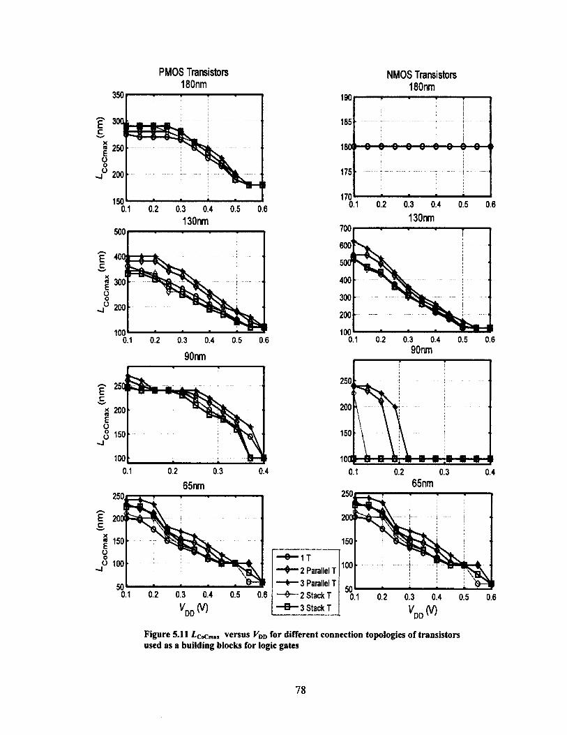
PMOS Transistors 180nm
90nm
350
| 250 oO
200
150
130nm
65nm
500
c <
| 300 oo
200
100*-0.1 0.2 0.3 0.4 0.5 0.6
Ec
200
•J100
0.1 0.2 0.3 0.4
NMOS Transistors 180nm
0.3 0.4
130nm700
600
400
300
200 ■
1000.2 0.3 0.4 0.5 0.6
90nm
250.
200
150
1001;0.1 0.2 0.3 0.4
65nm250.
150
100
0.2 0.3 0.5
2 Parallel T
3 Parallel T2 Stack T
3 Stack T
Figure 5.11 LcoCm»i versus FDD for different connection topologies of transistors used as a building blocks for logic gates
78

5.5 Chapter Summary
In this chapter we proposed a method to optimize the delay (or operation frequency)
of a digital circuit operating in the sub-threshold region. Our proposed method is based
on maximizing the CoC ratio by manipulating the channel lengths of transistors. First, we
biased different typical pull-up and pull-down networks that are used as building blocks
of digital gates, e.g., stack of three serial transistors or parallel connection of two
transistors. Then, we plotted CoC versus the channel length to find ZcoCmax for each type
of transistors in the four considered technologies. For all different topologies and for all
considered technology nodes, ZcoCmax is extracted based on simulation.
Due to the dependency of ZcoCmax to the supply voltage and the logic gate
configuration, one should decide to choose the correct ZcoCmax to optimize the
performance of the circuit. Although incorporating ZcoCmax does not result in the absolute
maximum frequency, the frequency obtained by using ZcoCmax is still within an acceptable
margin from the maximum frequency for all considered technologies.
Besides to performance and energy consumption improvement, the CoC method is
very time efficient in the delay optimizing for large digital circuits with numerous
transistors. The CoC method is based on DC simulations and is much faster than the
transient analysis that is used to find Zfmax- The CoC method opens a perspective for the
designers to choose a suitable starting point for simulation instead of doing blind
exhaustive and time consuming simulations.
79

6 Implications and Applications
In this chapter, we report the implications of our results and using the optimum
channel lengths obtained in Chapter 5 in some applications.
6.1 Increasing V DD versus Channel-length Manipulation
Verma et. al. in [64] claimed that using minimum-size transistors is the best choice
for sub-threshold circuits. They showed that to decrease the propagation delay along the
critical path, a slightly increase in the supply voltage from its minimum-energy point, is
more efficient than the conventional gradual sizing. Figure 6.1 verifies that claim, where
energy and frequency of a 29-INV RO is plotted versus Fdd in the 65 nm technology for
the minimum channel length. This plot shows two sets of simulation results, one for the
1500 ►000
1275 1500
■ 1000LU
500
CQQ» * t * g * * * _g * >q0.15 0.16 0.17 0.18 0.19 0.2 0.21 0.22 0.23 0.24 0.25
Figure 6.1 Energy per operation and frequency vs. KDD for a 29- INV RO in the 65 nm technology at Lmin=60 nm.
80

minimum size and the other for the channel width that maximize the frequency (obtained
by simulation). This plot shows that increasing the channel width, as it is the
conventional method of sizing, increases the frequency slightly for a large cost in the
energy consumption. Also, it shows that if Fdd increases from its minimum energy point,
0.17 V, to 0.2 V, energy is almost constant for about 100% increase in the frequency,
while keeping the size of the transistors minimum. This implies that one can increase the
supply voltage slightly from the minimum energy point to increase the performance
rather than increasing the channel width.
However, increasing the channel length will affect the delay and energy completely
differently from the way that the channel width does. As explained in Section 4.5,
increasing the channel length decreases the sub-threshold slope that makes the transistors
faster and shortens the short-circuit time. This leads to an improvement in the
performance for a small penalty in the energy. Figure 6.2 shows the energy and frequency
Energy and Frequency vs. VDD
1100 ---------
975
850Uj
725
6000.15 0.16 0.17 0.18 0.19 0.2 0.21 0.22 0.23 0.24 0.25
vu o MFigure 6.2 Energy per operation and frequency vs. VBD for a 29- INV RO in the 65 nm technology at fFmin=120 nm.
2250
1500
750Emin Point
minsizB
0 ^CoC V fCoC
^ /minsize
NX*
SI
versus F d d for a 29-INV RO simulated for two sets of transistor sizes in the 65 nm
technology at Wmm=\20 nm. Both sets show the same minimum-energy point located at
F d d= 0 . 1 7 V . Incorporating Z-coCmax from Table 5.1 in the RO does not change the
minimum energy, but increases the frequency by 78.7%. Additionally, increasing the
supply voltage from the minimum point to a larger value, e.g, F dd= 0 .1 9 V, results in an
83.3% increase in the frequency for only a 0.75% cost in the energy. This plot shows that
Verma’s claim is not valid for improving the performance by up-sizing the channel
length. For instance, if the up-sized circuit operates at F dd= 0 . 1 9 V , the frequency of
operation and energy are 750 KHz and 725 aJ, respectively. Suppose that one is
interested in exploiting the minimum-size circuit with increased supply voltage to
achieve the same performance. The plot shows that F dd should be increased to 0.22 V.
This results in an energy consumption of 863 aJ that is 10% above the energy
consumption caused by increasing the channel length to ZcoCmax operating at F dd= 0 .1 9 V.
Although in this research we are not discussing the energy minimizing in detail and
it will be presented in the future work, it is worth to show a graph for more clarification
on the effects of the channel length upsizing on the energy and performance of a circuit.
Parameter ZcoCmax presented in Table 5.1 does not necessarily result in the minimum
energy. Simulations show that the channel lengths where the energy becomes minimum
are longer than the minimum channel length and they differ from ZcoCmax- Using these
new sets of channel lengths obtained by simulation in a 29-INV RO, results in curves
illustrated in Figure 6.3. It shows that increasing the channel length moves the minimum-
energy point towards smaller supply voltages. In addition, using suitable channel lengths
reduces the minimum energy value by 15.8% while the performance increases compared
to the RO with minimum-size transistors.
Again, if we want to compare the effect of increasing F d d and increasing the channel
length, consider the case that the RO is upsized and operating in F d d= 0 .2 V. The
frequency and energy are 625 KHz and 740 aJ, respectively (point A). If we want to keep
the minimum size and increase the Fdd to have the same performance as point A, we
have to increase Fdd to 0.21 V (point B). At this point the energy is 830 aJ that is 12.2 %
more than upsized circuit operating at the lower voltage.
82

15001000
minsize
min-energy
900 .1875
■ 1250;
700 • 625
600'
Figure 6.3 Energy per operation and frequency vs. FDD for a 29- INV RO in the 65 nm technology at ff'„li„=120 nm.
Figure 6.4 depicts EDP curves versus Fdd for four different sets of transistor sizes. It
shows that using Z-coCmax and channel lengths resulting in the minimum energy leads to
smaller EDPs compare to circuits with minimum-size transistors or wider PMOS
transistors. Using Z-coCmax results in the smallest EDP values.
6.2 32-bit CLA Adder
The adder consists of eight similar blocks. Each block adds two 4-bit sets of the
inputs. For example, the first block takes A[l:4] and B[l:4] and Cin as its inputs and
produces S[l:4] and Cout as the outputs. Cout of the first block is fed to the next block
and summation is performed on this input and the next 4-bits of A and B (A[5:8] and
B[5:8]). The block diagram of a 4-bit CLA adder is shown in Figure 6.5. Group PG
83
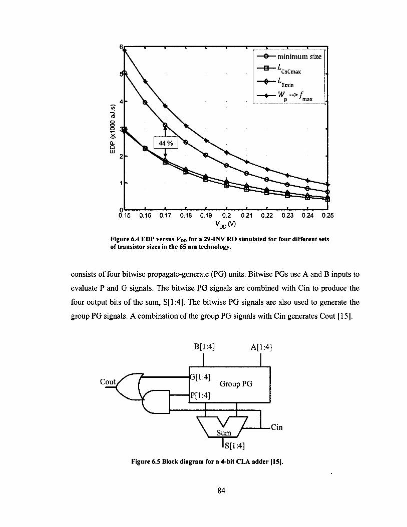
O— minimum size
CoCmax
L .Emm
w -->/n J rmax
</>“ 5CO
CLoUJ
44%
Figure 6.4 EDP versus for a 29-INV RO simulated for four different sets of transistor sizes in the 65 nm technology.
consists of four bitwise propagate-generate (PG) units. Bitwise PGs use A and B inputs to
evaluate P and G signals. The bitwise PG signals are combined with Cin to produce the
four output bits of the sum, S[l:4]. The bitwise PG signals are also used to generate the
group PG signals. A combination of the group PG signals with Cin generates Cout [15].
B[l:4] A[l:4]
Cout
Cin
G[l:4]
P[l:4]Group PG
Figure 6.5 Block diagram for a 4-bit CLA adder [15].
84

Each bitwise PG group consists of four NAND2 and three INV. A sum block consists
of 15 NAND2, 14 INV, and three NOR2. The group PG block has five NAND2, four
NOR2 and six INV. Hence, total adder has 192 NAND2, 56 NOR2, and 184 INVs. We
simulated the adder with three different sets of sizings. The first is an adder with
minimum-size transistors. In the second adder, the channel lengths are set to IcoCmax
presented in Table 5.1. And finally, the channel lengths for parallel and serial
combinations presented in Table 5.7 are incorporated in the adder as the third set. The
area of the first adder is 1869 pm2 [6]. Using IcoCmax from Table 5.1 and Table 5.7 in the
adder circuit, increases the area of the adder to 4900 pm2 (162% increase compared to
minimum-size adder) and 5390 pm2 (188% increase compared to minimum-size adder),
respectively. The channel width is fixed at its minimum value, Jrmjn=120 nm.
Table 6.1 shows the results of simulations. Using both sets of ZcoCmax improves the
delay, energy per operation, and EDP at the same time. None of these quality metrics are
degraded, similar to what happened for the ROs studied in Chapter 5. Using Z-coCmax in
the adder results in about 50%, 20%, and 60% improvements in the delay, energy, and
EDP, respectively. Incorporating XcoCmax from Table 5.7 improves the delay by 5%
compared to using IcoCmax from Table 5.1 for a cost of 20% increase in the area of the
adder.
Table 6.1 Simulation results for a 32-bit CLA adder in the 65 nm technology at KDD=0.2.
Minimum Size TcoCmax (Table 5.1) ^CoCmax (Table 5.7)
Test Case(ns)
E
( f j)
EDP(X10a J.S)
tp
(ns)
E
(f j)
EDP(X10a J.S) (ns)
E
( f j)
EDP(X1021 J.S)
A=0, B=1
Cin toggles2569 7.12 18.29 1310 5.69 7.45 1289 5.67 7.3
A, B, Cin
toggle the
same425 1.2 0.51 226 1.03 0.233 220 1 0.22
A=l, B& Cin toggle the
same
449 1.47 0.66 235 1.14 0.27 228 1.2 0.27
random 2780 8.25 22.93 1410 6.45 9.1 1385 6.42 8.9
85

6.3 Driving Large-Loads
Verma’s claim even becomes worse when a circuit drives large loads. Consider the
situation that a chain of inverters are driving an inverter 64 times larger than the
minimum-size inverter (representing a 64-bits data line). In the logical effort method
[15], it is shown that for driving a 64X inverter, the optimum number of stages is three
and the optimum tapering factor is V64 = 4. It means that to have the minimum delay in
driving a 64X inverter (load), the inverters in the chain should have channel widths one,
four, and 16 times wider than the minimum channel width. Since in this thesis we are
studying the channel length manipulation, we keep the channel width of transistors in
their minimum value. Two cases are studied to compare the effects of increasing the
supply voltage and upsizing the channel length. In the first case all inverters are
minimum size and in the second case the channel lengths are upsized to TcoCmax in Table
5.1 for the 65 nm technology. A square-wave signal is applied to the input node and the
propagation delays are measured between the output and input nodes shown in Figure
6.6. Table 6.2 shows the results of simulation. The first row shows the delay, power, and
energy consumption for the chain with minimum-size inverters. The second row is the
measurement results when ZcoCmax is used in the inverters of the chain. Pch and Ech refer
to the power and energy consumption in three inverters in the chain and Pl and Ei refer
to the power and energy consumption in the load. The table shows that incorporating
TcoCmax results in a 100% increase in the operation frequency (~ 50% reduction in delay).
Total energy consumption shows 11.6% reduction after using Z-coCmax in the inverters of
the chain.
Table 6.2 Simulation results for a three-inverters chain driving a large load at Fdd=0.2 V.
fplh fphl h fmax Pch Ech Pl El ■fitotal
ns ns ns KHz pW aJ pW aJ aJ
Min-size 673 167 420 250 133 531 177 710 1241
Z'CoCmax 355 83218.5 500
261 521 288 5761097
-48% 100% -11.6%
86

^iEaifuadM^
Figure 6.6 Driving a large load with a chain of three inverters.
Incorporating Z-coCmax in inverters leads to faster inverters and sharpens the rising and
falling edge of the signal at the output node as depicted in Figure 6.7. This results in a
shorter time of short-circuit current. Increasing the channel length, decreases both Ech and
Ei. If we want to use the minimum-size inverters in the chain and increase Fdd to have
the same performance as using upsized inverters, Fdd should increase to 0.225 V while
the supply voltage of load is not changed. Using the new supply voltage results in
0.2
0.18
0.16
0.14
® 0.12 XJ
0.08
0.06
0.04 min-size
CoCmax0.02
500 1500 2000 time (ns)
1000 2500 3000 3500 4000
Figure 6.7 Output signal of a chain driving a large load at FDD=0.2 V and 120 nm in the 65 nm technology.
87

1186 aJ total energy consumption energy, which is 7% more than of the chain with
upsized inverters and lower supply voltages.
In Figure 6.6 there is no off-path logic gates connected to the intermediate nodes
along the critical path. In practical cases, in each node of the critical path there are
usually some off-path connections. We repeated the same simulation as done before for
Figure 6.6, except that in nodes 1 and 2 we connected three other minimum-size inverters
in parallel. These inverters add loading effects to the nodes along the critical path. In
these kinds of circuits that there are some off-path connections along the critical path,
increasing the channel length is even more beneficial than increasing the supply voltage,
the results are reported in Table 6.3. to have a minim-size chain performing as the
upsized chain, one should increase the supply voltage to 227mV that results in a total
energy of 1377 aJ, which is 9% more than of upsized chain operating at lower Fdd-
Table 6.3 Simulation results for a three-inverters chain driving a large load at FDD=0.2 V. In each intermediate node three minimum-size inverters are connected in parallel as off- path logic gates.
fplh fphl h fmax Pch Ech Pl El £totalns ns ns KHz pW aJ pW aJ aJ
Min-size 749 247 498 250 144 574 200 800 1374
f-CoCmax 387 114250.5 487
283 581 330 6761257
-49.6% 94.8% -8.5%
6.4 Chapter Summary
Using ZcoCmax in the sub-threshold circuits reduces the energy consumption in
parallel to the improvement of the speed of circuit. This fact shows that the minimum
energy operation is not always associated with using minimum-size transistors in circuits
and increasing the supply voltage to compensate the lower speed, which is a popular
belief.
88

7 Conclusion
This chapter summarizes the research work’ contributions of this thesis, and proposed
future work, which will help researchers to advance the art of sub-threshold design for
next generation of electronic devices.
The rapidly growing portable-electronics market as well as thermal dissipation has
launched a massive trend towards low-power and low-voltage design techniques. Among
these techniques, the sub-threshold offers the minimum energy consumption for the cost
of speed, which is still acceptable for some ULP applications such as micro-sensor
networks and biomedical devices. Nevertheless, a number of research projects have been
established on increasing the speed of sub-threshold circuits to extend applications of
these kinds of circuits to relatively higher frequencies. Increasing the width of transistors
is the most common method to increase the speed of a digital circuit, besides increasing
Fod- In the sub-threshold region due to the INWE, manipulating the channel width needs
special consideration. The literature has been addressing the concept of manipulating the
channel width of transistors in sub-threshold circuits. However, manipulating the channel
length is not common in the super-threshold region, and in the sub-threshold region is a
very new topic. Changing the channel length affects different characteristics of a
transistor such as the threshold voltage, current, capacitance, and sub-threshold slope.
Each of these has its effect on the delay and energy consumption. In this thesis these
effects are studied in detail and a method for minimizing the delay in sub-threshold
circuits is proposed based on channel length manipulations.
7.1 Summary
Unlike the super-threshold design, where the channel length is mostly fixed at its
minimum, in the sub-threshold region the channel length can be increased to achieve a
higher driving current. This implies a possibility for a maximum in the current curve
versus the channel length. In the 180 nm technology, only the PMOS transistor shows a
89

maximum in the current versus the cannel length and the current for the NMOS transistor
is maximum at the minimum channel length. For the 130 nm and 90 nm technologies
both types of transistors show a maximum in their current curves versus the channel
length. In the 65 nm, where two “lvt” and “svt” flavours are offered, both transistors of
“svt” type show a descending behaviour with respect to the channel length, while
transistors of “lvt” type have maximum point in their current curves versus the channel
length.
Since the current has the main rule in the delay, it seems that maximizing the current
minimizes the delay. But this is not correct, because of the capacitances dependence to
the channel length. Since the delay is related to the ratio of capacitances over current, we
studied CoC to find an optimal channel length minimizing the delay.
In this thesis, a new method of CoC measurement is introduced. Applying this
method results in optimum channel lengths sets, ZcoCmax- Using LcoCmax in inverter ROs
leads to delays and frequencies relatively close to the minimum delay and maximum
frequency obtainable through simulations in Cadence. Although the CoC method is also
based on simulation in Cadence, it is a DC simulation and is very fast compare to doing
transient analysis to find the maximum frequency or minimum delay. Using ZcoCmax in a
29-INV RO results in a frequency only 2.5% less than the frequency obtained through
exhaustive simulations. Incorporating LcoCmax in a 29-INV RO improves the frequency up
to 95% compared to the minimum-size RO in the 130 nm technology.
A test bench for different combinations of transistor connections are also introduced
in the thesis. Digital logic gates usually contain two or three transistors connected in
series or parallel. Hence, we introduced new test-benches to find the optimum channel
lengths for different configurations. Depending on the topology of a logic gate, one can
decide to use appropriate channel lengths.
The CoC method shows its effectiveness when one wants to find the maximum
frequency for a large circuit with many transistors. For instance, a 32-bit CLA adder has
1360 transistors. Performing transient simulation to find the optimal channel lengths is
almost impossible. Using ZcoCmax in a 32-bit CLA adder results in a 50% improvement in
the delay in the 65 nm technology.
90

In addition, increasing the channel length improves the sub-threshold slope of a
transistor. Improved sub-threshold slope results in faster transistors with lower short-
circuit energy consumption. In most cases using ZcoCmax results in a lower energy
consumption compared to the minimum-size circuit. For example, in a 32-bit CLA adder,
incorporating Z-coCmax decreases the energy consumption by 20% and improves the EDP
by 60% compared to the minimum-size adder in the 65 nm technology.
7.2 Contributions
The following are the major contributions of this thesis.
1. Studying the effect of channel length manipulation on the current,
capacitances and sub-threshold slope in detail.
2. Introducing a method for obtaining the optimal channel length to minimize
the delay of a transistor.
3. Extending the above method to serial and parallel connections of transistors.
4. Introducing test benches and biasing techniques to find the optimal channel
lengths.
5. Applying the method to simple and complex circuits to prove the concept.
6. Demonstrating that in contrast to the popular belief, the minimum energy
operation is not always associated with minimum size transistors, and that it
can be lowered by manipulating channel length.
7. Increasing the speed of sub-threshold circuits that leads to extending the
application of these circuits to devices with relatively higher frequencies.
7.3 Future work
To continue the work presented in this thesis, the following research directions are
proposed.
1. Deriving an analytical model for finding ZcoCmax-
91

2. Improving the CoC method by considering the effect o f the transistor that is
going to its “off’ state.
3. Obtaining Z-coCmax for more complex combinations of transistors.
4. Introducing standard cell libraries based on optimum channel length.
5. Developing an analytical method to find the optimum channel length of
transistors in series and parallel.
6. Incorporating IcoCmax in different logic style such Pass-Transistor Logic
(PTL), Complementary Pass-Transistor logic (CPL), Dual Value Logic
(DVL), DCVSL, pseudo NMOS, and dynamic logic.
7. Developing a logical effort method for sub-threshold circuits based on the
channel length6.
8. Studying the effect of the channel length manipulation on the energy and
power consumption in detail.
9. Developing an analytical method for finding the channel length resulting in
the minimum energy.
10. Investigating the effect of channel length manipulation on noise and
robustness of digital logic gates operating in the sub-threshold region.
11. Investigating the optimal layout techniques for sub-threshold circuits.
12. Combining channel length manipulation with Parallel-Transistor-Stack (PTS)
[82]
13. Replacing the super-threshold-based ISC AS test benches with test benches
suitable for sub-threshold operation.
14. Performing Monte Carlo simulation to explore the effect of channel length on
PVT variations.
15. Exploring Layout-Dependant (LOD) proximity effect on the performance of
long transistors.
Finally, it is obvious that this work can be easily extended to design various ULP
analog circuits operating in the sub-threshold region.
6 conventional logical effort is based on the channel width
92

List o f References
[1] J. Burr and A. Peterson, "Energy Consideration in Multiple-Module Based
Multiprocessors," in IEEE Conference on Computer Design Digest for Technical
Papers, pp. 593-600,1991.
[2] J.-J. Kim and K. Roy, "Double Gate-MOSFET Sub-threshold Circuit for Ultra-Low-
Power Applications," IEEE Transactions on Electron Devices, vol. 51, no. 9, pp.
1468-1474,2004.
[3] V. De and S. Borkar, "Technology and Design Challenges for Low-Power and High-
performance Microprocessors," International Symposium on Low-power Electronics
and Design, pp. 163-168, 1999.
[4] J. Kwong, Y. Ramadass, N. Verma, M. Koesler, H. Moorman, and A. P.
Chandrakasan, "A 65 nm sub-Vt microcontoller with integrated SRAM and
Switched-capacitor DC-DC Converter," IEEE Intl. Solid-State Circuits Conference,
pp. 318-319,2008.
[5] H. Soeleman and K. Roy, "Digital CMOS Logic Operation in the Sub-Threshold
Region," Department of Electrical and Computer Engineering, West Lafayette, IN
47907, USA, 2000.
[6] M. Muker, "Sub-Threshold CMOS Logic Design Using Parallel Transistor Stacks,"
in Masters' thesis, Dept. Electronics, Carleton University, 2010.
[7] M. Nabvi, "Designing Faster CMOS Sub-threshold Circuits Using Transistor Sizing
and Parallel Transitor Stacks," in Masters' Thesis, Dept, Electronics, Carleton
University, 2012.
[8] T.-H. Kim, J. Keane, H. Eom, and C. H. Kim, "Utilizing Reverse-Short-Channel-
Effect for Optimal Subthreshold Circuit Design," IEEE Transaction on VLSI
Systems, pp. 821-829, JULY 2007.
[9] S. Keller, S. Siddharth, C. Moore and A. J. Martin, "Reliable Minimum-Energy
CMOS Circuit Design," in Varill 2nd European Workshop on CMOS Variability,
2011 .
93
[10] S. Hanson, M. Seok, D. Sylvester and D. Blaauw, "Nanometer Device Scaling in
Subthreshold Logic and SRAM," IEEE Transaction on Electron Devices, vol. 55,
no. l,pp . 175-185,2008.
[11] D. Bol, R. Ambroise, D. Flandre and J.-D. Legat, "Channel Length Upsize for
Robust and Compact Sub-threshold SRAM," Microelectronics laboratory, Universite
catholique de Louvain, Louvain-la-Neuve, Belgium, 2011.
[12] "An interview with Jack Kilby," Texas Instrument, available at
www.ti .com/corp/dpcs/kilbyctr/interview.shtml.
[13] G. E. Moore, "Cramming More Components onto Itegrated Circuits," Electronics,
vol. 38, no. 8, pp. 114-117,1965.
[14] R. Dennard et. al, "Design of Ion-implanted MOSFETs with Very Small Physical
Dimensions," Journal o f Solid State Circuits, vol. 9, no. 5, pp. 256-268, 1974.
[15] N. H. E. Weste and D. M. Harris, CMOS VLSI Design, A Circuits and Systems
Perspective, Toronto: Addison-Wesley, 2011.
[16] "List of CPU power dissipation figures," available at
http://en.wikipedia.org/wiki/List_of_CPU_power_dissipation_figures.
[17] Y. Pu, "On the Road towards Robust and Ultra Low Energy CMOS Digital Circuits
Using Sub/Near Threshold Power Supply," PhD Thesis Dissertation, Eindhoven
University of Technology, 2009.
[18] C. Piguet, "History of Low-power Electronics," in Low-Power Electronics Design,
pp. CRC Press 11-15,2005.
[19] A. P. Chandrakasan and R. W. Broederson, Low-power CMOS Desin, Wiely-IEEE
Press, January 1998.
[20] R. Wieinstein, "RFID: A Technical Overview and Its Application to the Enterprise,"
IT Professional, vol. 7, no. 3, pp. 27-33,2005.
[21] A. Mainwaring, J. Polastre, R. Szewczyk, D. Culler and J. Anderson, "Wireless
Sensor Networks for Habitat Monitoring," ACM International Workshop on Wireless
Sensor Networks and Applications (WSNA), pp. 88-97,2002.
[22] "[Online]. Available at http://www.alertsystems.org/".
94

[23] K. Chintalapudi, E. Johnson and R. Govindan, "Structural Damage Detection Using
Wireless Sensor-Actuator Networks," in Proceedings o f the IEEE International
Symposium on Intelligent Control, 2005.
[24] L. Schwiebert, S. Gupta and J. Wienmann, "Reseach Challange in Wireless
Networks of Biomedical Sensors," Mobile Computing and Networking, pp. 151-165,
2001.
[25] I. Korhonen, J. Parkka and M. Van Gils, "Health Monitoring in the Home of the
Future," IEEE Engineering Mediciene and Biology, vol. 22, no. 3, pp. 66-73,2003.
[26] R. Hahn and H. Reichel, "Batteries and Power Supplies for Wearable and
Ubiquitous Computing," in Proc. 3rd Int. Symp. Wearable Computers, pp 168-169,
1999.
[27] M. Hempstead, N. Tripathi, P. Mauro, G. Wei and D. Brooks, "An Ultra-Low-Power
System Architecture for Sensor Network Applications," in Proc. Intl. Symp. on
Computer Architecture, pp. 208-219,2005.
[28] H. Kulah and K. Najafi, "An Electromagnetic Micro Power Generator for Low-
Frequency Environment Vibrations," in Proc. o f the IEEE Intl. Conf. for Micro
Elctro-MechanicalSystems, pp 237-240,2004.
[29] S. Roundy, P. Wright and J. Rabbaey, "A Study of Low Level Vibrations as a Power
Source for Wireless Sensor Nodes," in Computer Communications, vol. 26, no. 11,
pp. 1131-1144,2003.
[30] S. Meninger, J. Mur-Miranda, R. Amirtharajah, A. Chandrakasan and J. Lang,
"Vibration-to-Electric Energy Conversion," IEEE transaction on Very Large Scale
Integration (VLSI), vol. 9, no. 1, pp. 64-76,2001.
[31] H. Bottner, J. Numus, A. Gavrikov, G. Kuhner, M. Jagle, C. Kunzel, D. Eberhard,
G. Plescher, A. Schubert and K.-H. Schlereth, "New Thermostatic Component Using
Microsystems Technologies," 1EEEJASME Journal o f Microelectronics Systems, vol.
13, no. 3, pp. 414-420,2004.
[32] "Panasonic Solar Cells Technical Handbook ’98/'99," Matsushita Battery Industrial
Co., Ltd., Aug. 1998.
95

[33] R. M. Swanson and J. D. Meindl, "Ion-implanted compllementary MOS transistors
in low-voltage circuits," IEEE Journal o f Solid State Circuits (JSCC), vol. 7, no. 2,
pp. 146-153,1972.
[34] R. Swanson, "Complementary MOS Transistors in Micropower Circuits," PhD
dissertation, Stanford University, 1974.
[35] B. Zhai, D. Blaauw, D. Sylvester and K. Flautner, "Theoretical and Practical Limits
of Dynamic Voltage Scaling," DAC, pp. 7-11,2004.
[36] B. H. Calhoun, A. Wang and A. Chandrakasan, "Modeling and Sizing for Minimum
Energy Operation in Subthreshold Circuits," IEEE Journal o f Solid State Circuits,
vol. 40, no. 9, pp. 1778-1786, Sep 2005.
[37] J. T. Kao, M. Masayuki and A. P. Chandrakasn, "A 175-mV Multiply-accumulate
Unit Using an Adaptive Supply Voltage and Body-Bias Architecture," IEEE Journal
o f Solid State Circuits, vol. 37, no. 11, pp. 1545-1554,2002.
[38] E. A. Vittoz and J. Fellarth, "New Analog CMOS IC's Based on Weak-inversion
Operation," in European Solid-State Circuits Conference, pp. 12-13, 1976.
[39] E. A. Vittoz, "Origin of Weak-inversion (or sub-threshold) Circuit Design," in Sub
threshold Design for Ultra-Low-Power Systems, A. P. Chandrakasan, Springer,
2005, pp. 11-23.
[40] H. Soeleman and K. Roy, "Ultra-low Power Digital Sub-threshold Logic Circuits,"
in Proc IEEE/ACM Intl. Symp. Low-Power Electronics and Design, pp. 94-96,1999.
[41] J. Wang and B. H. Calhoun, "Techniques to Extend Canary-based Standby VDD
Scaling for SRAMs to 45 nm and beyond," IEEE Journal o f Solid State Circuits,
vol. 43, no. 11, pp. 2514-2523,2008.
[42] B. H. Calhoun and A. Chandrakasan, "Ultra-Dynamic Voltage Scaling Using Sub
threshold Operation and Local Voltage Dithering," IEEE Journal o f Solid State
Circuits, vol. 41, no. 1, pp. 238-245,2006.
[43] B. H. Calhoun et al., "Flexible Circuits and Architecture for Ultra-Low-Power," in
Proceeding IEEE, vol. 98, no. 2, pp. 267-282,2010.
[44] B. Zhai, R. G. Dresliniski, D. Blaauw, T. Mudge and D. Sylvester, "Energy Efficient
96
Near-threshold Chip Multi-processing," Proceeding IEEE/ACM Intl. Symposium
Low-power Electronics and Design, pp. 32-37,2007.
[45] H. Lee, Y. J. Park, H. S. Min, H. Shin and D. Kang, "Reduction of Reverse-Short-
Channel-Effect in High-Energy Implanted Retrograde Well," Journal o f the Korean
Physical Society, vol. 40, no. 4, pp. 629-652,2002.
[46] K. Roy, S. Mukhopadhhyay and H. Mahmoodi-Meimand, "Leakage Current
Mechanisms and Leakage Reduction Techniques in Deep-Submicrometer CMOS
Circuits," in Proceedings o f The IEEE, 2003.
[47] B. C. Paul, A. Raychowdhury and K. Roy, "Device Optimization for Digital Sub
threshold Logic," IEEE Transactions on Electron Devices, vol. 52, no. 2, pp. 237-
247,2005.
[48] S. Luan, H. Liu, R. Jia and J. Wang, "Two-dimensional Sub-threshold Current
Model for Dual-material Gate SOI nMOSFETs with Single Halo," Front. Electr.
Electron. Eng. China, pp. 98-103,2009.
[49] A. Massimo, "Understanding DC Behavior of Subthreshold CMOS Logic Through
Closed-Form Analysis," IEEE Tranasactions on Circuits and Systems, pp. 1597-
1607, July 2010.
[50] D. M. Harris, B. Keller, J. Karl and S. Keller, "A Transregional Model for Near-
Threshold Circuits with Application to Minimum-energy Operation," in 22nd
International Conference on Microelectronics (ICM 2010), ,2010.
[51] J. Meindel and J. A. Davis, "The Fundemental Limit on Binary Switching Energy
for Terascale Integration (TSI)," IEEE Journal o f Soild State Circuits, vol. 35, no.
10, pp. 1515-1516,2000.
[52] M.Muker and M. Shams, "Designing Digital Sub-threshold CMOS Circuits Using
Paralle Transistor Stacks," Electronics Letters, vol. 47, no. No. 6,2011.
[53] M.Nabavi and M. Shams, "A Gate Sizing and Transistor Fingering Strategy for Sub
threshold CMOS Circuits," 1EICE Journal o f Electronics Express (ELEX), accepted
2012.
[54] J.Zhou, S. Jayapal, J. Stuyt, J. Huisken and H. de Groot, "The Impact of Inverse-
97

Nairow-Width-Eeffect on Sub-threshold Device Sizing," IEEE DAC, pp. 267-272,
2011 .
[55] H.K.O.Berge and S. Aunet, "Benefits of Decomposing Wide CMOS Transistors into
Minimum-size G a te s NORCHIP, pp. 1-4,2009.
[56] J. Keane, H. Eom, T. H. Kim, S. Sapatnekar and C. Kim, "Sub-threshold Logical
Effort: A Systematic Framework for Optimal Sub-threshold Device Sizing," in
DAC'06, San Fransisco, California, USA, 2006.
[57] C. Giacomotto and V. G. Oklobdzija, "Logic Style Comparison for Ultra Low Power
Applications," Advanced Computer Systems Engineering Laboratory, Department of
Electrical and Computer Engineering, University of California, Davis, CA 95616.
[58] H. Soeleman, K. Roy and B. C. Paul, "Robust Sub-threshold Logic for Ultra-Low-
Power Operation," IEEE Transactions on Very Large Scale Integration, vol. 9, no. 1,
pp. 90-99,2001.
[59] A. Pajkanovic, T. Kazmierski and B. Dokic, "Adiabatic Digital Circuits Based on
Sub-threshold Operation of Pass-transistor and Slowly Ramping Signals," in
Proceedings o f Small Systems Simulation Symposium, Nis, Serbia, 2012.
[60] J. Chen, L. T. Clark and Y. Cao, "Robust Design of High Fan-in/Out Sub-threshold
Circuits," in International Conference on Computer Design (ICCD’05), 2005.
[61] M. R. Bagheri, "Ultra Low Power Sub-threshold Bridge Style Adder in Nanometer
Technologies," Canadian Journal on Electrical and Electronics Engineering, vol. 2,
no. 7, pp. 294-299,2011.
[62] A. Tajalli, E. Brauer, Y. Leblebici and E. Vittoz, "Sub-threshold Source-Coupled
Logic Circuits for Ultra-Low-Power Applications," IEEE Transactions o f Solid-state
Circuits, vol. 43, no. 7, pp. 1699-1710,2009.
[63] J. Nyathi and B. Bero, "Logic Circuits Operating in Sub-threshold Voltages," in
ISLPED'06, Tegemsee, Germany, 2006.
[64] N. Verma, J. Kwong and A. P. Chandrakasan, "Nanometer MOSFET Variation in
Minimum-Energy Sub-threshold Circuits," IEEE Transactions on Electron Devices,
vol. 55, no. 1, pp. 163-174,2008.
98

[65] A. Wang and A. P. Cahndrakasan, "Optimal Supply and Threshold Scaling for
Subthreshold CMOS Circuits," Proceedings o f the IEEE Computer Society Annual
Symposium on VLSI (ISVLSI’02), 2002.
[66] D. Bol, "Robust and Energy-Efficient Ultra-Low-Voltage Circuit Design under
Timing Constraints in 65/45 nm CMOS," Journal o f Low Power Electronics and
Applications, pp. 1-19,2011.
[67] D. Bol, D. Kamel, D. Flandre and J.-D. Legat, "Nanometer MOSFET Effects on the
Minimum-Energy Point of 45nm Sub-threshold Logic," in ISLPED’09, San
Francisco, California, USA, 2009.
[68] D. Bol, R. Ambroise, D. Flandre and J.-D. Legat, "Impact of Technology Scaling on
Digital Sub-threshold Circuits," IEEE Computer Society Annual Symposium on
VLSI, pp. 179-184,2008.
[69] B. Calhoun and A. P. Cahndarkasan, "Characterizing and Modeling Minimum
Energy Operation for Sub-threshold Circuits," in ISLPED'04, Newport Beach,
California, USA, 2004.
[70] J. Chen, L. T. Clark and T. H. Chen, "An Ultra-Low-Power Memory with a Sub-
threshold Power Supply Voltage," IEEE Journal o f Solid State Circuits, vol. 41, no.
10, pp. 2344-2353,2006.
[71] B. H. Calhoun and A. P. Chandrakasan, "A 256kb Sub-threshold SRAM in 65 nm
CMOS," in ISSCC'06, pp. 2592-2601, San Francisco, California, USA, 2006.
[72] G. Wang and et al., "A 0.127 umA2 high performance 65 nm SOI based embedded
DRAM for on-processor applications," in Proc. Intl. Electron Device Meeting, 2006.
[73] J. Zhou, S. Jayapal, B. Busze, L. Huang and J. Stuyt, "A 40 nm Inverse-Narrow-
Width-Effect-Aware Sub-Threshold Standard Cell Library," in DAC’l l , June 5-10,
2011, San Diego, California, USA.
[74] P. Xiaonan Zhang, "Designing Low-power Standard Cell Library With Improved
Drive Granularity," Qualcomm availabale at "www.design-reuse.com".
[75] W. Shockley, "A unipolar field effect transistor," in Proc. IRE, 1952.
[76] T. Sakurai and A. R. Newton, "Alpha-Power-Law MOSFET Model and Its
99
Application to CMOS Inverter and other Fomulas," IEEE Journal o f Solid State
Circuits, vol. 25, pp. 584-594, Apr 1990.
[77] B. Razavi, Design of Analog CMOS Integrated Circuits, Boston: Me Graw Hill,
2001.
[78] A. B. Bhattacharyya, Compact MOSFET Models for VLSI Design, Asia: John
Wiley & Sons, 2009.
[79] D. W.Greve, Field Effect Devices and Aplications, London: Printice-Hall, 1998.
[80] Y.Tisividis, Operation and Modeling of the MOS Transistors, Boston: McGraw-Hill,
1999.
[81] J. M. Rabaey, A. Chandrakasan and B. Nikolic, Digital Integrated Circuits, A Design
Perspective, London: Prentice Hall, 2003.
[82] A. Bellaouar and M. I. Elmasry, Low-Power Digital VLSI Design, Massachusetts:
Kluwer Academic Publishers, 1995.
100