designing polyphase dpd solutions with 28-nm fpgas · designing polyphase dpd solutions with ......
TRANSCRIPT

January 2012 Altera Corporation
WP-01171-1.0
© 2012 Altera Corporation. AlQUARTUS and STRATIX worOffice and in other countries. respective holders as describedproducts to current specificatioproducts and services at any tiof any information, product, oadvised to obtain the latest verfor products or services.
101 Innovation DriveSan Jose, CA 95134www.altera.com
Designing Polyphase DPD Solutions with28-nm FPGAs
White Paper
This white paper describes how to design an efficient polyphase and non-polyphase digital predistortion (DPD) feed-forward path solution with Altera® 28-nm FPGAs, especially the Arria® V family of FPGAs. In addition, a resource usage and power comparison between different architectures is provided to facilitate design tradeoffs.
IntroductionThe ever-increasing use of smart phones and devices is driving exponential growth in mobile data traffic. As Figure 1 shows, mobile networks will soon approach 4000 petabytes per month.
Figure 1. Data Growth in Mobile Networking
Source:(1) Cisco Visual Networking Index: Global Mobile Data Traffic Forecast Update, Cisco, 9 February 2010
Because the current mobile infrastructure cannot keep pace with the growing demand, basestation providers need to upgrade their digital front end (DFE) radio equipment to support wider and wider RF bandwidths. In addition, increasing pressure on operators to reduce operating expenses (OPEX) and the trend towards green technology are driving the need for more power-efficient solutions in the DFE radio head.
Peta
byte
s Pe
r Mon
th
4000
3500
2500
3000
2000
1500
1000
500
0
2008 2009 2010 2011 2012 2013 2014 2015Year
l rights reserved. ALTERA, ARRIA, CYCLONE, HARDCOPY, MAX, MEGACORE, NIOS, ds and logos are trademarks of Altera Corporation and registered in the U.S. Patent and Trademark All other words and logos identified as trademarks or service marks are the property of their
at www.altera.com/common/legal.html. Altera warrants performance of its semiconductor ns in accordance with Altera's standard warranty, but reserves the right to make changes to any
me without notice. Altera assumes no responsibility or liability arising out of the application or use r service described herein except as expressly agreed to in writing by Altera. Altera customers are sion of device specifications before relying on any published information and before placing orders
Feedback Subscribe
ISO 9001:2008 Registered
Page 2 Introduction
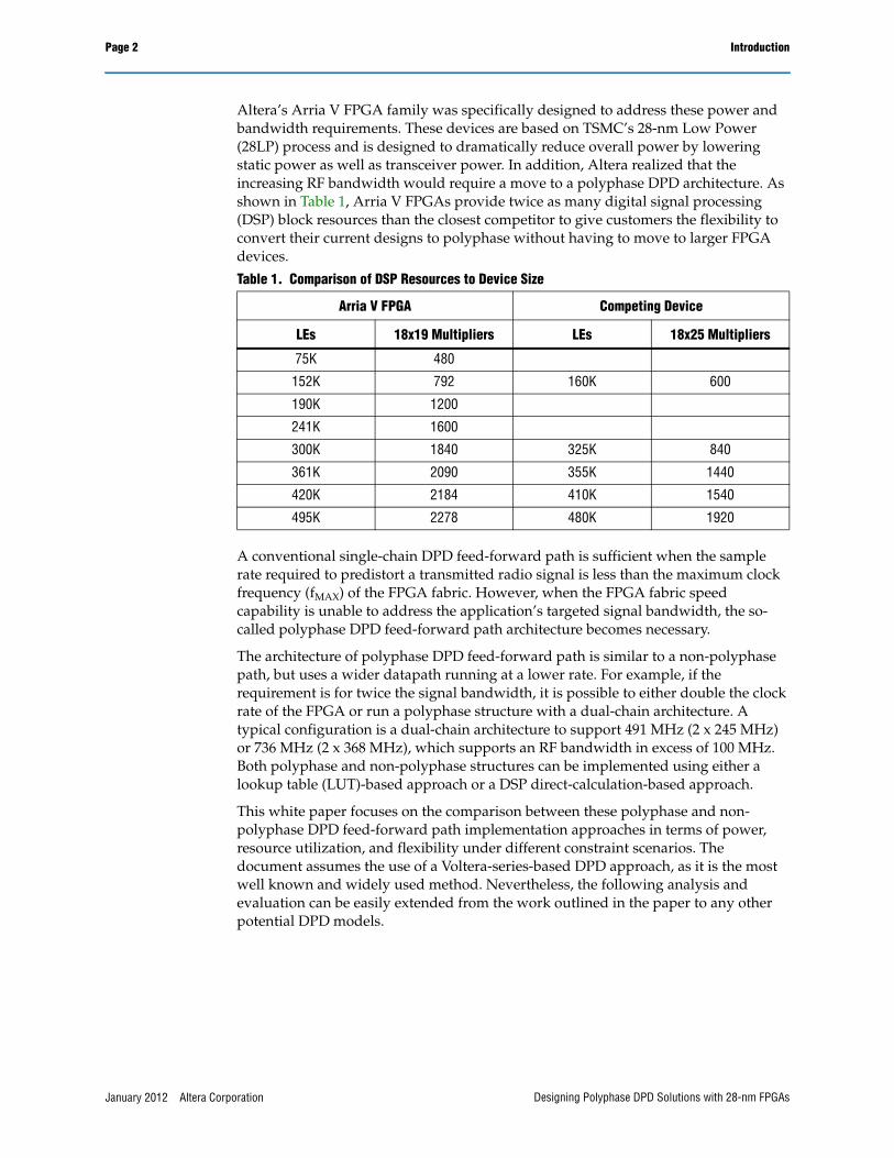
Altera’s Arria V FPGA family was specifically designed to address these power and bandwidth requirements. These devices are based on TSMC’s 28-nm Low Power (28LP) process and is designed to dramatically reduce overall power by lowering static power as well as transceiver power. In addition, Altera realized that the increasing RF bandwidth would require a move to a polyphase DPD architecture. As shown in Table 1, Arria V FPGAs provide twice as many digital signal processing (DSP) block resources than the closest competitor to give customers the flexibility to convert their current designs to polyphase without having to move to larger FPGA devices.
A conventional single-chain DPD feed-forward path is sufficient when the sample rate required to predistort a transmitted radio signal is less than the maximum clock frequency (fMAX) of the FPGA fabric. However, when the FPGA fabric speed capability is unable to address the application’s targeted signal bandwidth, the so-called polyphase DPD feed-forward path architecture becomes necessary.
The architecture of polyphase DPD feed-forward path is similar to a non-polyphase path, but uses a wider datapath running at a lower rate. For example, if the requirement is for twice the signal bandwidth, it is possible to either double the clock rate of the FPGA or run a polyphase structure with a dual-chain architecture. A typical configuration is a dual-chain architecture to support 491 MHz (2 x 245 MHz) or 736 MHz (2 x 368 MHz), which supports an RF bandwidth in excess of 100 MHz. Both polyphase and non-polyphase structures can be implemented using either a lookup table (LUT)-based approach or a DSP direct-calculation-based approach.
This white paper focuses on the comparison between these polyphase and non-polyphase DPD feed-forward path implementation approaches in terms of power, resource utilization, and flexibility under different constraint scenarios. The document assumes the use of a Voltera-series-based DPD approach, as it is the most well known and widely used method. Nevertheless, the following analysis and evaluation can be easily extended from the work outlined in the paper to any other potential DPD models.
Table 1. Comparison of DSP Resources to Device Size
Arria V FPGA Competing Device
LEs 18x19 Multipliers LEs 18x25 Multipliers
75K 480
152K 792 160K 600
190K 1200
241K 1600
300K 1840 325K 840
361K 2090 355K 1440
420K 2184 410K 1540
495K 2278 480K 1920
January 2012 Altera Corporation Designing Polyphase DPD Solutions with 28-nm FPGAs
DPD Background Page 3
Furthermore, this paper introduces a novel DSP direct-calculation-based architecture for the feed-forward path of the DPD solution, which is capable of reducing significantly the resource usage in comparison to the traditional approach as described in the current literature [1,2,3,4]. This new architecture exploits the vast DSP resources of Arria V FPGAs and addresses the high power consumption and resource usage often associated with the DSP direct calculation, turning it into a feasible and favorable solution for remote radio head (RRH) systems.
DPD BackgroundIn the modern radio access networks (RANs), improving the power efficiency of the system is increasingly important. This improved efficiency is driven by the trend towards green technologies, as well as providing a reduction of operating expenses occurred with service operators through lower cooling costs and power bills. Due to the technical difficulties of designing high-power linear power amplifiers (PAs), DPD techniques are often used to compensate for the non-linearity of PAs. The DPD technology aims to increase the efficiency of the PA by enabling it to be operated in the saturated region (non-linear region) without introducing unacceptable performance degradation. The popularity of DPD technology is mainly derived by the lower cost of implementation and flexibility in comparison to other methods such as feed-forward. Because the bandwidth of a pre-distorted signal is much higher (typically at least five times) than the transmitted signal bandwidth, one of the greatest challenges in FPGA-based DPD implementation is to meet the increasingly large bandwidths with the FPGA fabric’s limited speed performance, while keeping the resource usage as low as possible.
A DPD solution includes three major areas: PA behavioral modeling, tuning the DPD model parameters to fit the PA model, and implementation. Modeling the behavior of the PA is the algorithmic basis of a DPD solution, the step of tuning the model parameters can be regarded as the calibration/optimization of the mathematic model for better matching the analog feature of the system, and the implementation of DPD is to map the calibrated DPD algorithms into the real-time signal processing blocks in the digital domain with hardware.
There are generally two main approaches to the behavioral modeling of a PA: stochastic methods and analytical schemes. In this paper, all the discussions and analysis are based on the analytical modeling approach, which is easier to characterize than stochastic methods. This method uses a predetermined PA model to characterize the PA behavior, while the model parameters are determined by a curve-fitting exercise. The most well-known and widely used mathematical model is the Voltera series model, which is capable of capturing the power and memory characteristics of a PA. Other models that are less complex are the Wiener and Hammerstein models [6,7].
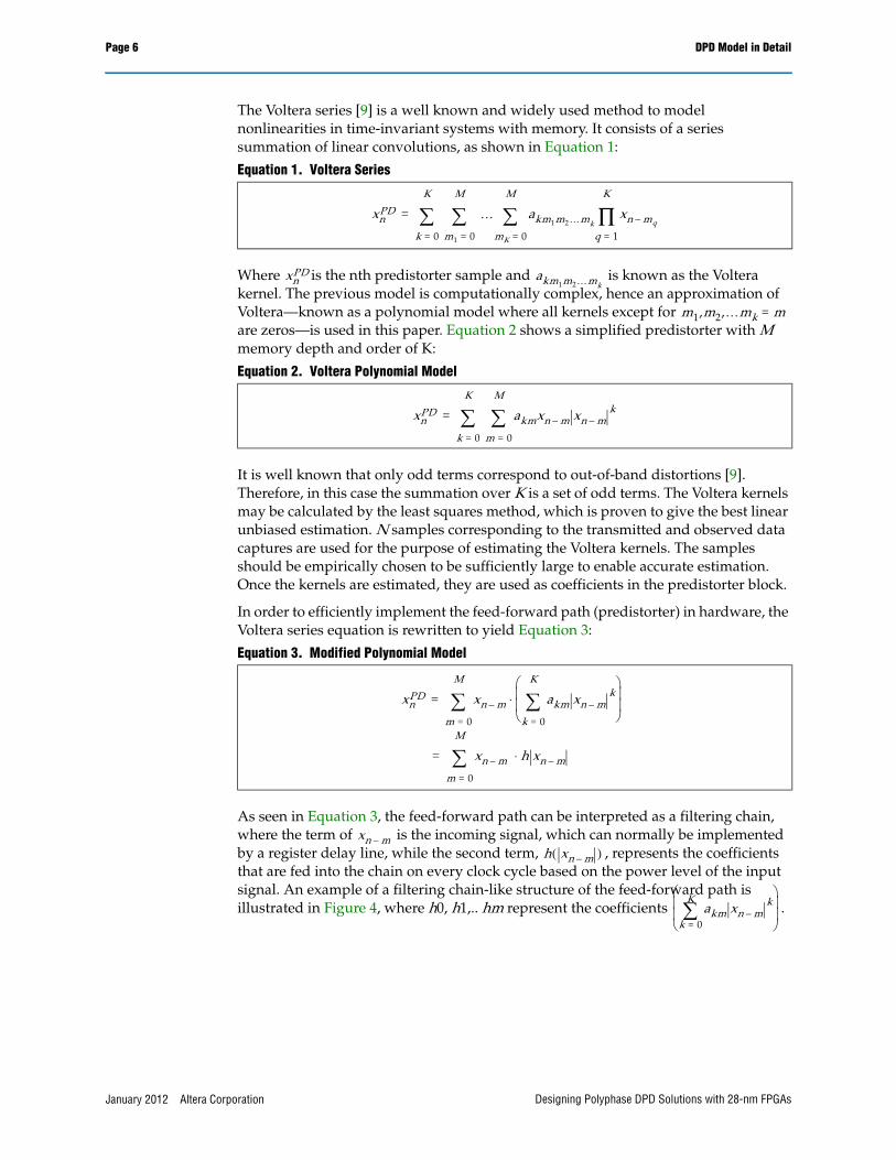
Figure 2 shows an example of a typical RRH system, where the DPD split into a so-called DPD feed-forward path module and a DPD coefficient calculation module. The DPD feed-forward path pre-distorts the signal to compensate the nonlinear and memory effects of the PA in advance using the coefficients derived from the tuning stage performed in the coefficient calculation module.
January 2012 Altera CorporationDesigning Polyphase DPD Solutions with 28-nm FPGAs
Page 4 DPD Background
Figure 2. Example of DPD Architecture in RRH Application
Typically, the sample rate required for the DPD feed-forward path is approximately five to seven times the bandwidth of the transmitted signal. This means that, for a 60-MHz transmitted signal bandwidth, the DPD feed-forward path’s sample rate is approximately 300 to 420 Msps.
As the radio signal bandwidth has been significantly increasing during the recent years and is still expected to follow this trend in the future, the difficulty of implementation of the feed-forward path becomes more and more evident in hardware, because the sample rate eventually will exceed the FPGA fabric clock rate limit. However, it is still possible to map the high sample-rate requirements of the DPD feed-forward path to an FPGA device, where the clock is lower than the sample rate, by using a polyphase approach. The polyphase technique has been employed in many digital signal filter applications before, however, the cost and power of using such an approach relative to a non-polyphase one is not yet well understood. In addition, the DPD feed-forward path has more complex data dependency in comparison to typical filter structures.
The basic idea of the polyphase approach is to split the incoming data samples into multiple (in this case, dual) parallel signal processing chains. The data throughput, and hence the fMAX, required to process the samples is much lower than a non-polyphase approach. After the data have been functionally processed in parallel, the multiple pre-distorted signal streams are recombined using the half-data-rate serializer/deserializer (SERDES) blocks in the FPGA I/O blocks before being output to the DAC.
CPU (Housekeeping, Operation, Admin, and Maintenance)
CPRI/OBSAI
DUC MixerDPD
Feed-ForwardFilter
DACInterface
FeedbackADC
Interface
ADCInterface
DDC
ReceiverMeasurements
Single Instance
Multiple Instances
FPGA Logic
CPU Subsystem
CFR
DPDCoefficientCalculation
January 2012 Altera Corporation Designing Polyphase DPD Solutions with 28-nm FPGAs

DPD Model in Detail Page 5
In the process of tuning the DPD model to match the PA, a least square approach is usually used to evaluate the parameters of the analytical model. In this case, the Voltera model is targeted, mainly because of its best linear unbiased estimation [8]. The PA characteristics are assumed to remain unchanged during one parameter’s adaption period, when the DPD coefficient calculation module shown in Figure 2 performs the coefficient calculation. The fine-tuning is performed periodically, which means that the DPD model is adaptive to any potential PA changes. This is achieved by observing the output of the PA and adapting the DPD model to the observed changes in PA behavior. In Figure 2, the feedback ADC interface (observation path) captures the output of the PA, which is then fed into the tuning block as the DPD coefficient calculation component. Since the computation/tuning of the coefficients in the DPD analytical model is performed periodically, the selected data samples are typically buffered before the subsequent calculations are performed. If a single coefficient’s tuning block is unable to meet the timing and throughput requirement in the observation path, similar parallel computational structures may be employed to implement the required tuning calculations.
DPD Model in DetailThis section provides a more in-depth look at the DPD, including an overview of the feed-forward path architecture and its implementation for targeting the Voltera series model. The DPD operation is undertaken in baseband, and as shown in Figure 3, it consists of two main parts: the feed-forward predistorter and the adaption module. The predistorter models the inverse of PA behavior. When considering high sample rates and increased computational complexity, a hardware-mapped implementation of the predistorter is the only available option. The adaption block is responsible for the estimation and update of the PA behavioral model parameters used in the predistorter. The data captured from transmitter, , and observation receiver, , are assumed to be aligned.
Figure 3. DPD Functional Block Diagram in Transmitter
xn yn
Baseband Data
Digital Predistortion
Predistorter DAC UpConvertor Amplifier
Observation Receiver
DownConvertorADCAdaption
Coefficients
yn
xn
January 2012 Altera CorporationDesigning Polyphase DPD Solutions with 28-nm FPGAs
Page 6 DPD Model in Detail
The Voltera series [9] is a well known and widely used method to model nonlinearities in time-invariant systems with memory. It consists of a series summation of linear convolutions, as shown in Equation 1:
Where is the nth predistorter sample and is known as the Voltera kernel. The previous model is computationally complex, hence an approximation of Voltera—known as a polynomial model where all kernels except for are zeros—is used in this paper. Equation 2 shows a simplified predistorter with M memory depth and order of K:
It is well known that only odd terms correspond to out-of-band distortions [9]. Therefore, in this case the summation over K is a set of odd terms. The Voltera kernels may be calculated by the least squares method, which is proven to give the best linear unbiased estimation. N samples corresponding to the transmitted and observed data captures are used for the purpose of estimating the Voltera kernels. The samples should be empirically chosen to be sufficiently large to enable accurate estimation. Once the kernels are estimated, they are used as coefficients in the predistorter block.
In order to efficiently implement the feed-forward path (predistorter) in hardware, the Voltera series equation is rewritten to yield Equation 3:
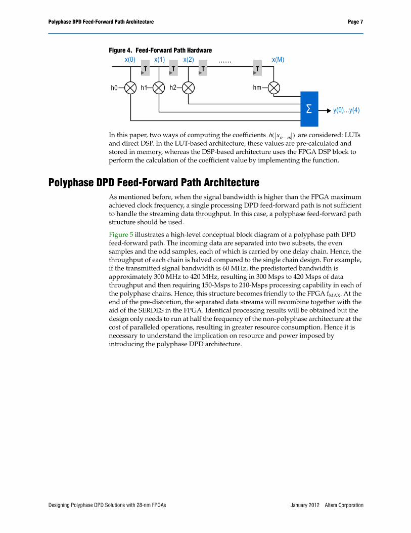
As seen in Equation 3, the feed-forward path can be interpreted as a filtering chain, where the term of is the incoming signal, which can normally be implemented by a register delay line, while the second term, , represents the coefficients that are fed into the chain on every clock cycle based on the power level of the input signal. An example of a filtering chain-like structure of the feed-forward path is illustrated in Figure 4, where h0, h1,.. hm represent the coefficients .
Equation 1. Voltera Series
Equation 2. Voltera Polynomial Model
Equation 3. Modified Polynomial Model
xnPD
k 0=
K
m1 0=
M
… akm1m2…mk
mK 0=
M
xn mq–
q 1=
K
∏=
xnPD akm1m2…mk
m1,m2,…mk m=
xnPD
k 0=
K
akmxn m–
m 0=
M
xn m–k=
xnPD xn m–
m 0=
M
akm
k 0=
K
xn m–k
xn m–
m 0=
M
h xn m–⋅=
⋅=
xn m–h xn m–( )
akmk 0=
K xn m–
k
January 2012 Altera Corporation Designing Polyphase DPD Solutions with 28-nm FPGAs
Polyphase DPD Feed-Forward Path Architecture Page 7
Figure 4. Feed-Forward Path Hardware
In this paper, two ways of computing the coefficients are considered: LUTs and direct DSP. In the LUT-based architecture, these values are pre-calculated and stored in memory, whereas the DSP-based architecture uses the FPGA DSP block to perform the calculation of the coefficient value by implementing the function.
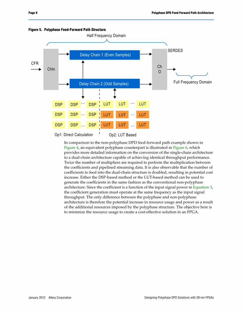
Polyphase DPD Feed-Forward Path ArchitectureAs mentioned before, when the signal bandwidth is higher than the FPGA maximum achieved clock frequency, a single processing DPD feed-forward path is not sufficient to handle the streaming data throughput. In this case, a polyphase feed-forward path structure should be used.
Figure 5 illustrates a high-level conceptual block diagram of a polyphase path DPD feed-forward path. The incoming data are separated into two subsets, the even samples and the odd samples, each of which is carried by one delay chain. Hence, the throughput of each chain is halved compared to the single chain design. For example, if the transmitted signal bandwidth is 60 MHz, the predistorted bandwidth is approximately 300 MHz to 420 MHz, resulting in 300 Msps to 420 Msps of data throughput and then requiring 150-Msps to 210-Msps processing capability in each of the polyphase chains. Hence, this structure becomes friendly to the FPGA fMAX. At the end of the pre-distortion, the separated data streams will recombine together with the aid of the SERDES in the FPGA. Identical processing results will be obtained but the design only needs to run at half the frequency of the non-polyphase architecture at the cost of paralleled operations, resulting in greater resource consumption. Hence it is necessary to understand the implication on resource and power imposed by introducing the polyphase DPD architecture.
x(0) x(1) x(2) x(M)
y(0)...y(4)
TTT T
h0 h1 h2 hm
�
......
h xn m–( )
January 2012 Altera CorporationDesigning Polyphase DPD Solutions with 28-nm FPGAs
Page 8 Polyphase DPD Feed-Forward Path Architecture
Figure 5. Polyphase Feed-Forward Path Structure
In comparison to the non-polyphase DPD feed-forward path example shown in Figure 4, an equivalent polyphase counterpart is illustrated in Figure 6, which provides more detailed information on the conversion of the single-chain architecture to a dual-chain architecture capable of achieving identical throughput performance. Twice the number of multipliers are required to perform the multiplication between the coefficients and pipelined streaming data. It is also observable that the number of coefficients to feed into the dual-chain structure is doubled, resulting in potential cost increase. Either the DSP-based method or the LUT-based method can be used to generate the coefficients in the same fashion as the conventional non-polyphase architecture. Since the coefficient is a function of the input signal power in Equation 3, the coefficient generation must operate at the same frequency as the input signal throughput. The only difference between the polyphase and non-polyphase architecture is therefore the potential increase in resource usage and power as a result of the additional resources imposed by the polyphase structure. The objective here is to minimize the resource usage to create a cost-effective solution in an FPGA.
....
....
....
....
....
....
Half Frequency Domain
Full Frequency Domain
Delay Chain 1 (Even Samples)
Delay Chain 2 (Odd Samples)
ChO
SERDES
ChlnCFR
DSP DSP DSP
DSP DSP DSP
DSP DSP DSP
LUT LUT LUT
LUT LUT LUT
LUT LUT LUT
Op1: Direct Calculation Op2: LUT Based
January 2012 Altera Corporation Designing Polyphase DPD Solutions with 28-nm FPGAs

LUT Solution Page 9
Figure 6. Polyphase Feed-Forward Path Example
LUT SolutionThe LUT-based solution uses the input-signal power level to choose the coefficient values, which are stored in pre-calculated LUTs. LUTs can be efficiently implemented on an FPGA device by utilizing the built-in memory blocks, which are indexed by the normalized power of the transmitted signal. The LUT contents are periodically updated by an adaption step, which is referred as the tuning procedure mentioned previously. The benefits of the LUT-based solution over its DSP-based counterpart will be discussed in the subsequent section, but can be summarized as:
■ Reduction of required multiplications and hence, the utilized multipliers
■ Enhanced flexibility of run-time polynomial order programmability
■ Low latency of coefficient generation
Coefficient generation for the filter chain is expressed in Equation 4, where K denotes the maximum supported order of polynomials:
h4h3h2h1h0
h4h3h2h1h0
TTT
�
�
Even Samplesx(0), ,x(4) x(-2), x(0), x(-4), x(-2), x(0)
y(0), ,y(4)
y(1), ,y(5)
Odd Samplesx(1), x(3), x(5) x(-1), x(1), x(3) x(-13), x(-1), x(1)
Y(0) = h0*Y(1) = h0*Y(2) = h0*Y(3) = h0*
x(0) + h1*x(1) + h1*x(2) + h1*x(3) + h1*
x(-1) + h2*x(0) + h2*x(1) + h2*x(2) + h2*
x(-2) + h3*x(-1) + h3*x(0) + h3*x(1) + h2*
x(-3) + h4*x(-2) + h4*x(-1) + h4*x(0) + h3*
x(-4)x(-3)x(-2)x(-1)
T T T
Equation 4. Coefficient Function
h xn m–( ) akm
k 0=
K
xn m–k=
January 2012 Altera CorporationDesigning Polyphase DPD Solutions with 28-nm FPGAs
Page 10 LUT Solution
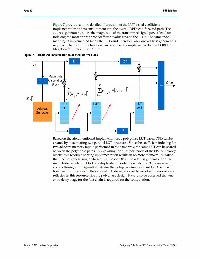
Figure 7 provides a more detailed illustration of the LUT-based coefficient implementation and its embodiment into the overall DPD feed-forward path. The address generator utilizes the magnitude of the transmitted signal power level for indexing the most appropriate coefficient values inside the LUTs. The same index mapping is implemented for all the LUTs and, therefore, only one address generator is required. The magnitude function can be efficiently implemented by the CORDIC MegaCore® function from Altera.
Figure 7. LUT-Based Implementation of Predistorter Block
Based on the aforementioned implementation, a polyphase LUT-based DPD can be created by instantiating two parallel LUT structures. Since the coefficient indexing for two adjacent memory taps is performed in the same way, the same LUT can be shared between the polyphase paths. By exploiting the dual-port mode of the FPGA memory blocks, this resource-sharing implementation results in no more memory utilization than the polyphase single-phased LUT-based DPD. The address generator and the magnitude calculation block are duplicated in order to satisfy the 2X increase in system throughput. Figure 8 illustrates the polyphase feed-forward DPD path and how the optimizations to the original LUT-based approach described previously are reflected in this resource-sharing polyphase design. It can also be observed that one extra delay stage for the first chain is required for the computation.
X n
X nk X n
k��k=0
k=0
K
k,0��K
k,m-1X n-m+1
Z’ (n)k
m m+1LUTLUTLUT
1AddressGenerator
MagnitudeCalculation
Block
Z-1 Z-1
Z-1Z-1
January 2012 Altera Corporation Designing Polyphase DPD Solutions with 28-nm FPGAs

DSP Solution Page 11
Figure 8. Structure of Polyphase LUT-Based Predistorter
DSP SolutionDespite the advantageous resource sharing exploited by the LUT-based DPD approach, the FPGA memory resources are usually expensive and relatively scarce to the extent that their utilization is likely to be the main resource bottleneck in a FPGA-based RRH implementation. Therefore, a different implementation approach based on DSPs is essential. Such an approach would provide extra design space and allow for a more balanced utilization among the heterogeneous resources available on the FPGA device.
In order to show how a DSP-based efficient solution can be designed to calculate the coefficients, Equation 4 can be unrolled (Equation 5) to show its efficient nesting approach:
k=0��K
k,(m-1)X (n-m+1)
kX n/2
k��k=0
K
k,0
X nk
Z’ (n)
Z’ (n-1)
X n X n-2X n-M /2
X n-M /2
X n-1
MagnitudeCalculation
Block
Z-1 Z-1Z-1
Z-1 Z-1
Z-1
Z-1
MagnitudeCalculation
Block
AddressGenerator
AddressGenerator
LUTM-1
LUT0
LUT1
LUTm+1
Z-1 Z-1
Z-1
LUTM
LUTm
January 2012 Altera CorporationDesigning Polyphase DPD Solutions with 28-nm FPGAs

Page 12 DSP Solution
This new expression of the coefficient equation uncovers a nesting approach of calculating , which can be realized by introducing a multiply-add structure as the basic processing unit, shown in Figure 9. This unit fits efficiently within the variable-size DSP block in Altera’s Arria V or Stratix® V families of FPGAs, since the built-in pre-adder and post-accumulator in the DSP block can absorb an addition operation cascaded before or after the multiplication. Moreover, the variable DSP block can be configured in different modes, enabling the computations of higher fixed-point or even floating-point precisions.
Figure 9. Basic Operation Unit for Coefficient Calculation
More specifically, it is very common to consider only odd polynomial terms for the coefficient calculation. This allows for a significant reduction of the computational complexity, since the even terms correspond to out-of-band distortions, with the exception of the zero order term. For example, the designer might consider applying the polynomial order of {0, 1, 3, 5, 7} to the Voltera model, thus turning Equation 5 into Equation 6:
By utilizing the basic operation unit, an efficient hardware architecture can be designed, as shown in Figure 10. The total number of instantiated DSP blocks can be significantly reduced by feeding the path with the squared value of the signal power level rather than with its first order. Otherwise, the designer can still use the Equation 6 to calculate all the terms, although nearly half of them are zeros.
Figure 10. Example of Optimized Coefficient Calculation Using the Basic Unit
Equation 5. DSP Efficient Coefficient Calculation
h xn m–( ) akm
k 0=
K
xn m–k
a0,m xn m–+ a1,m xn m–+ a2,m xn m–+( ) … ak,m xn m–+( )⋅( )⋅ ⋅( )⋅( )=
=
h xn m–( )
Equation 6. Efficient Coefficient Direct Calculation Example
h xn m–( ) a0,m a1,m+ xn m– a3,m xn m–3 a5,m xn m–
5 a7,m xn m–+ + +7
a0,m xn m–+ a1,m xn m–2+ a3,m xn m–
2+ a5,m xn m–2+ a7,m xn m–
2+( )⋅( )⋅( )⋅( )⋅=
=
xn-m
a7,m a5,m a1,ma3,m a0,m
xn-mh
xn-m2
( )
January 2012 Altera Corporation Designing Polyphase DPD Solutions with 28-nm FPGAs
DSP Solution Page 13
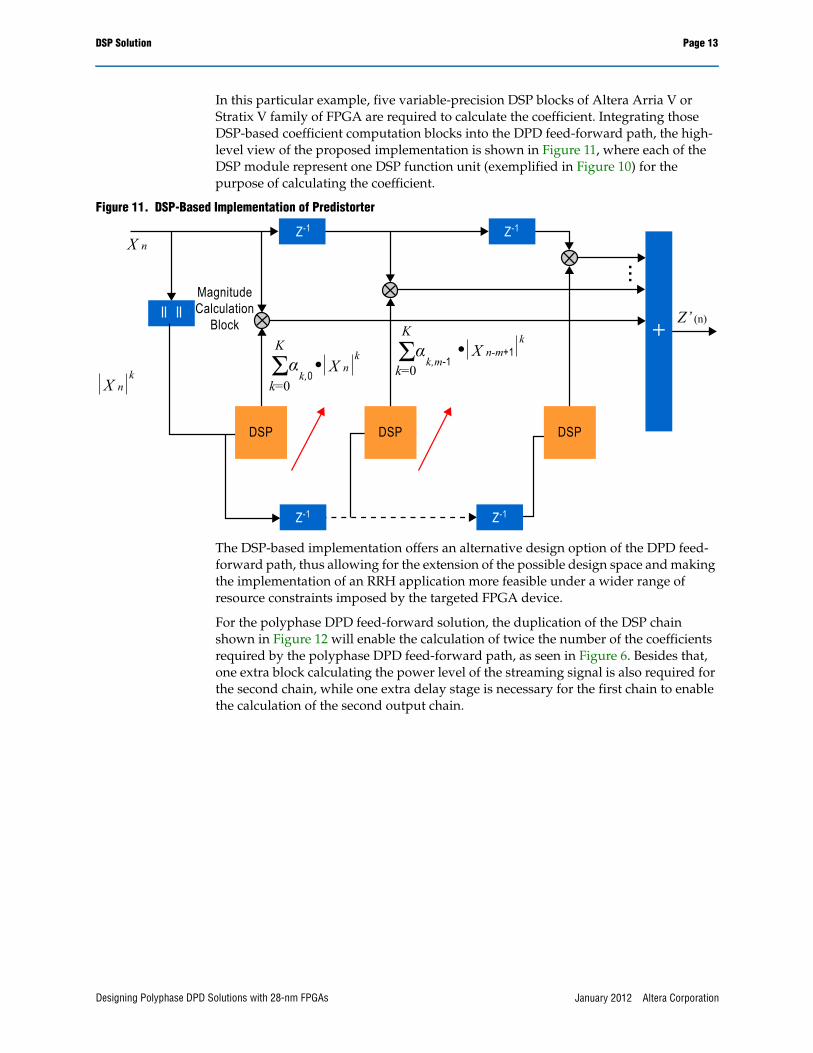
In this particular example, five variable-precision DSP blocks of Altera Arria V or Stratix V family of FPGA are required to calculate the coefficient. Integrating those DSP-based coefficient computation blocks into the DPD feed-forward path, the high-level view of the proposed implementation is shown in Figure 11, where each of the DSP module represent one DSP function unit (exemplified in Figure 10) for the purpose of calculating the coefficient.
Figure 11. DSP-Based Implementation of Predistorter
The DSP-based implementation offers an alternative design option of the DPD feed-forward path, thus allowing for the extension of the possible design space and making the implementation of an RRH application more feasible under a wider range of resource constraints imposed by the targeted FPGA device.
For the polyphase DPD feed-forward solution, the duplication of the DSP chain shown in Figure 12 will enable the calculation of twice the number of the coefficients required by the polyphase DPD feed-forward path, as seen in Figure 6. Besides that, one extra block calculating the power level of the streaming signal is also required for the second chain, while one extra delay stage is necessary for the first chain to enable the calculation of the second output chain.
X n
X nk X n
k��k=0
k=0
K
k,0��K
k,m-1X n-m+1
Z’ (n)k
MagnitudeCalculation
Block
Z-1
Z-1Z-1
DSP DSP DSP
Z-1
January 2012 Altera CorporationDesigning Polyphase DPD Solutions with 28-nm FPGAs

Page 14 Power Comparison Between Different Architectures
Figure 12. Structure of Polyphase DSP-Based Predistorter
Power Comparison Between Different ArchitecturesAs seen from the previous discussion, the option to use the LUT-based architecture or DSP-based architecture is valid for both polyphase and non-polyphase scenarios, so the designer can select either depending on constraints and metrics such as the bandwidth, the polynomial depth, the number of memory terms, etc. It is assumed that with the increasing bandwidths required in RRH systems, the adoption of polyphase architecture will eventually become inevitable for the FPGA-based DPD feed-forward path implementations. Therefore this section will discuss quantifying the cost and power benefits of selecting either the LUT approach or the DSP direct calculation approach under different scenarios.
One of important measures used to select between architectures is the power of the architecture. Based on the comparison between the DSP-based feed-forward path architecture and the LUT-based feed-forward path architecture, it is clearly seen that the only difference between the two is how the coefficients are calculated in Equation 4. In the LUT approach, any order of polynomial may be implemented using the same LUT structure, whereas in the DSP approach, increasing the order of the polynomial implemented results in an increase in the number of multipliers and calculations that need to be performed. Therefore, there is a power break-even point between these two different options as the order of polynomial increases. Figure 13
Z’ (n)
Z’ (n+1)
X nk
X n+1k
X n
X n-1
MagnitudeCalculation
Block
Z-1
MagnitudeCalculation
Block
Z-1 Z-1 Z-1
DSP
Z-1
Z-1
DSP
Z-1
DSP
DSP
DSP DSP
DSP
Z-1
Z-1
DSPDSP
DSP
Z-1
DSP
DSP
January 2012 Altera Corporation Designing Polyphase DPD Solutions with 28-nm FPGAs
Power Comparison Between Different Architectures Page 15
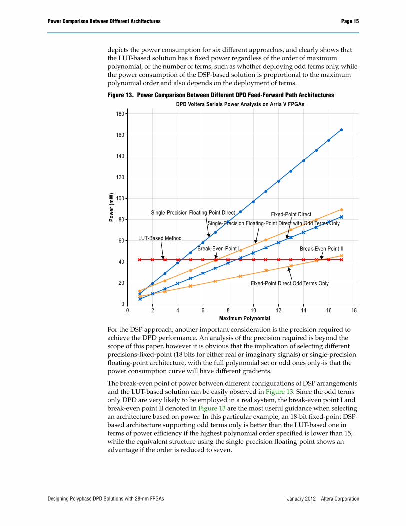
depicts the power consumption for six different approaches, and clearly shows that the LUT-based solution has a fixed power regardless of the order of maximum polynomial, or the number of terms, such as whether deploying odd terms only, while the power consumption of the DSP-based solution is proportional to the maximum polynomial order and also depends on the deployment of terms.
Figure 13. Power Comparison Between Different DPD Feed-Forward Path Architectures
For the DSP approach, another important consideration is the precision required to achieve the DPD performance. An analysis of the precision required is beyond the scope of this paper, however it is obvious that the implication of selecting different precisions-fixed-point (18 bits for either real or imaginary signals) or single-precision floating-point architecture, with the full polynomial set or odd ones only-is that the power consumption curve will have different gradients.
The break-even point of power between different configurations of DSP arrangements and the LUT-based solution can be easily observed in Figure 13. Since the odd terms only DPD are very likely to be employed in a real system, the break-even point I and break-even point II denoted in Figure 13 are the most useful guidance when selecting an architecture based on power. In this particular example, an 18-bit fixed-point DSP-based architecture supporting odd terms only is better than the LUT-based one in terms of power efficiency if the highest polynomial order specified is lower than 15, while the equivalent structure using the single-precision floating-point shows an advantage if the order is reduced to seven.
DPD Voltera Serials Power Analysis on Arria V FPGAs180
160
140
120
100
80
60
40
20
00 2 4 6 8 10 12 14 16 18
Maximum Polynomial
Powe
r (m
W)
Single-Precision Floating-Point Direct Fixed-Point DirectSingle-Precision Floating-Point Direct with Odd Terms Only
Break-Even Point IIBreak-Even Point I
LUT-Based Method
Fixed-Point Direct Odd Terms Only
January 2012 Altera CorporationDesigning Polyphase DPD Solutions with 28-nm FPGAs

Page 16 Resource Usage Comparison Between Different Architectures
More specifically, Table 2 shows the power consumption of different feed-forward path architectures supporting two parallel transmitters. For all the DSP-based approaches, it is assumed that only odd terms up to eleven and the zero-order term are included. Note that the power difference among these options are to the same scale. This is because that the dynamic power, which is proportional to the hardware frequency, dominates the final power result: only half of the hardware clock speed is required by the polyphase design compared to its non-polyphase counterpart, leading to similar power consumption values, even though the resource of the polyphase solution is nearly doubled.
Resource Usage Comparison Between Different ArchitecturesResource usage is one of the most important factors to be considered when evaluating the different DPD feed-forward path architectures. Table 2 lists the resource utilization of six different DPD feed-forward path architectures, and assumes that the highest polynomial order is eleven and the polynomial equations only include odd terms excepting the zero-order term. It also assumes that the LUT architecture uses a LUT with 2048 entries, the DSP fixed-point architecture uses 18-bit fixed-point numbers and the floating-point architecture is single precision. Table 3 shows that the DSP architecture consumes more DSP blocks and less memory than the LUT architecture.
Table 2. Power Comparison of Different DPD Feed-Forward Path Architectures
Architecture # of Instances Power (W) fMAX (MHz)
Non-Polyphase Fixed-Point DSP 2 1.5 245.76
Non-Polyphase Floating-Point DSP 2 3.9 245.76
Non-Polyphase Fixed-Point LUT 2 1.3 245.76
Polyphase Fixed-Point DSP 2 2.0 122.88
Polyphase Floating-Point DSP 2 4.9 122.88
Polyphase Fixed-Point LUT 2 1.4 122.88
Table 3. Resource Estimate for Different DPD Feed-Forward Path Architectures
Resource Estimates for DPD Feed-Forward Path
Logic DSP Distributed Memory Block Memory
ALUTs LEs2 18x18
Multipliers
Memory ALUTs M9K M20K
Forward Path Non-Polyphase
Fixed-Point DSP 2200 2400 114 170 5 3
Floating-Point DSP 46800 83400 225 320 10 5
LUT 4300 4300 20 320 109 52
Forward Path Polyphase
Fixed-Point DSP 4400 4800 226 340 10 6
Floating-Point DSP 48100 84700 450 340 10 5
LUT 5900 5900 21 340 109 52
January 2012 Altera Corporation Designing Polyphase DPD Solutions with 28-nm FPGAs
Resource Usage Comparison Between Different Architectures Page 17
In considering the DSP-based approach, it can also be seen that the polyphase DSP-based solution uses approximately twice the number of the DSP blocks than the non-polyphase architecture. The additional resources used by the polyphase approach are mainly consumed by a duplicate set of coefficient calculations, while the incremental memory is imposed by the second CORDIC component used for magnitude computation but the overall undertaken memory resource is still small. The floating-point implementation is very expensive in terms of logic, so it may not be the appropriate option if the design is very cost sensitive. However, the floating-point solution will enable better precision and higher dynamic range for a better DPD predistortion performance, and is likely to be required to meet the performance requirements for DPD.
In considering the LUT-based approach, it can be seen that relatively few DSP blocks are used, but the memory resource usage is relatively high. Importantly, it is noted that the resource difference between polyphase- and non-polyphase-based LUT architectures is small, which means twice the system throughput can be obtained easily with only a modest incremental cost.
In analyzing the data, the following observations can be made. The floating-point DSP solution has the highest resource utilization. Depending on the multiplier and memory usage in the remainder of the design, the DSP- or LUT-based solution can be employed.
When applying a polyphase structure, the LUT-based architecture requires only a small increase in resource usage relative to the non-polyphase LUT-based approach. This is because the LUT-based architecture does not require an increase in the amount of memory when supporting the polyphase approach, because the same memory can be used for both delay chains with a dual-port FPGA memory block. A modest increase in logic usage is due to the additional delay chain in the polyphase approach and a second CORDIC core. Hence, based on FPGA resource utilization, a LUT structure is the preferred architecture for a polyphase approach.
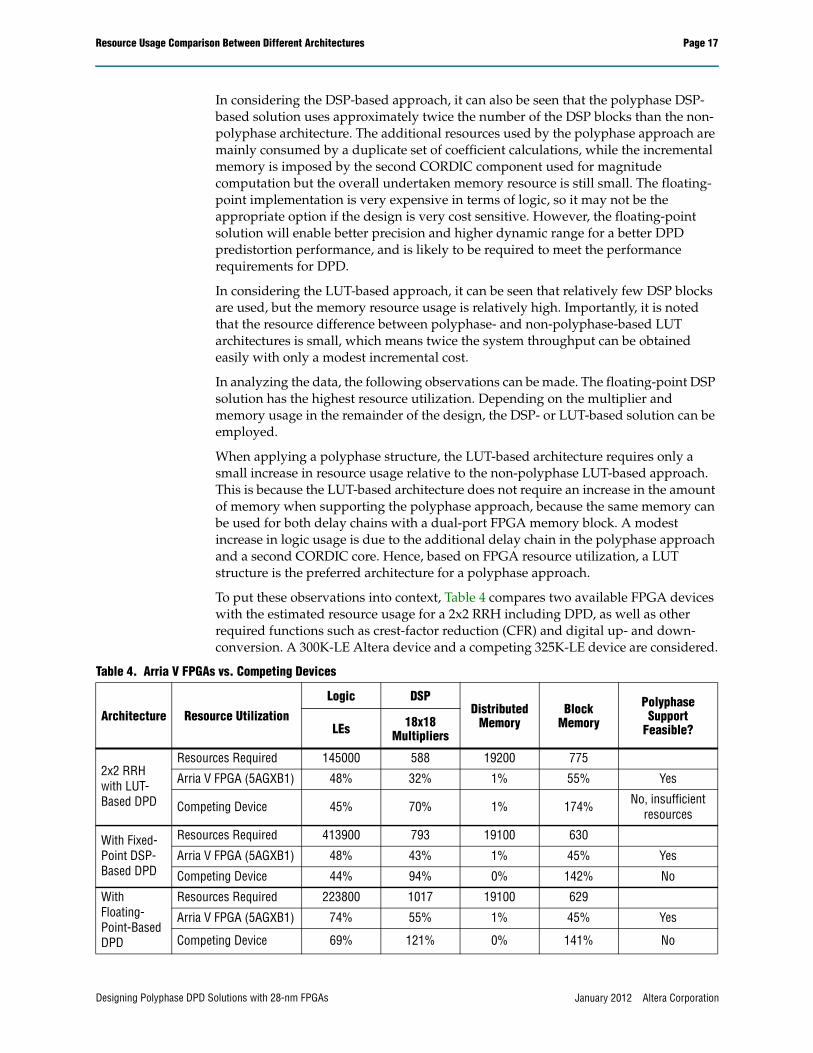
To put these observations into context, Table 4 compares two available FPGA devices with the estimated resource usage for a 2x2 RRH including DPD, as well as other required functions such as crest-factor reduction (CFR) and digital up- and down-conversion. A 300K-LE Altera device and a competing 325K-LE device are considered.
Table 4. Arria V FPGAs vs. Competing Devices
Architecture Resource Utilization
Logic DSPDistributed
MemoryBlock
Memory
Polyphase Support
Feasible?LEs 18x18 Multipliers
2x2 RRH with LUT-Based DPD
Resources Required 145000 588 19200 775
Arria V FPGA (5AGXB1) 48% 32% 1% 55% Yes
Competing Device 45% 70% 1% 174% No, insufficient resources
With Fixed-Point DSP-Based DPD
Resources Required 413900 793 19100 630
Arria V FPGA (5AGXB1) 48% 43% 1% 45% Yes
Competing Device 44% 94% 0% 142% No
With Floating-Point-Based DPD
Resources Required 223800 1017 19100 629
Arria V FPGA (5AGXB1) 74% 55% 1% 45% Yes
Competing Device 69% 121% 0% 141% No
January 2012 Altera CorporationDesigning Polyphase DPD Solutions with 28-nm FPGAs
Page 18 Conclusion
ConclusionIn order to meet the increasing bandwidth requirements for future radio system architectures, a polyphase architecture for the DPD feed-forward path is required. This paper introduces DPD fundamentals and shows how to develop a efficient DPD feed-forward path either by the DSP-based architecture or the LUT-based architecture, and introduced a novel direct DSP calculation method that enables the, the DSP-based feed-forward path to be easily realized by the variable-size DSP blocks on Altera FPGA devices. Furthermore, the power and cost of different architectures has been provided and design guidance for selecting architectures for various conditions. This guidance can be summarized as the following:
■ Polyphase DPD implementation can be effectively utilized where the required signal bandwidth exceeds the maximum clock rate of the FPGA implementing the radio DFE circuit. A typical configuration is a dual-chain architecture to support 491 MHz (2 x 245 MHz) or 736 MHz (2 x 368 MHz), which would support an RF bandwidth in excess of 100 MHz.
■ In general, polyphase-based architectures have higher resource usage than equivalent non-polyphase designs. Depending on the resource (memory, multipliers, or logic), a polyphase architecture uses 1.0 to 1.35 times the requirements of a non-polyphase design. The additional resource requirement for a polyphase DSP-based approach is more significant, with nearly twice the DSP multipliers necessary. Altera supports these requirements by offering multiplier-rich FPGAs, optimized for radio applications
■ The power consumption of the polyphase architectures is only marginally higher than the equivalent non-polyphase architecture. Although additional resources are required, their clock rate is half that of an equivalent non-polyphase design, resulting in lower dynamic power consumption.
■ Overall, when considering whether a LUT-based approach or a DSP-based approach is the most appropriate for a design, multiple factors need to be considered, including the maximum order of polynomial to use, the DPD performance requirements, and the relative cost and power tradeoffs.
■ In a typical system where RF bandwidths of greater than 60 MHz are being considered and an 11th-order polynomial is used, the polyphase LUT approach is the preferable option because it provides an architecture that will scale to higher bandwidths and is only marginally higher in power and resource consumption. The non-polyphase DSP direct-calculation-based architecture is similar in cost relative to the non-polyphase LUT-based architecture.
Regardless of which polyphase approach is taken, Altera has the resources to meet that need.
January 2012 Altera Corporation Designing Polyphase DPD Solutions with 28-nm FPGAs

References Page 19
References1. K.J. Muhonen, M. Kavehrad, and R. Krishnamoorthy, “Look-up table techniques
for adaptive digital predistortion: a development and comparison,” IEEE Transactions on Vehicular Technology, pp. 1995-2002, 2000.
2. Sung Won Chung, J.W. Holloway, and J.L. Dawson, “Energy-Efficient Digital Predistortion With Lookup Table Training Using Analog Cartesian Feedback,” IEEE Transactions on Microwave Theory and Techniques, vol. 56, no. 10, pp. 2248 - 2258, 2008.
3. P.L. Gilabert, A. Cesari, G. Montoro, E. Bertran, and J.-M. Dilhac, “Multi-Lookup Table FPGA Implementation of an Adaptive Digital Predistorter for Linearizing RF Power Amplifiers With Memory Effects,” IEEE Transactions on Microwave Theory and Techniques, vol. 56, no. 2, pp. 372 - 384, 2008.
4. G. T. Zhou, D. R. Morgan, et al. L. Ding, “A robust digital baseband predistorter constructed using memory polynomials,” IEEE Transactions on Communications, vol. 52, no. 1, pp. 159-165, 2004.
5. M. Rawat, K. Rawat, and F.M. Ghannouchi, “Adaptive Digital Predistortion of Wireless Power Amplifiers/Transmitters Using Dynamic Real-Valued Focused Time-Delay Line Neural Networks,” IEEE Transactions on Microwave Theory and Techniques, vol. 58, no. 1, pp. 95-104, 2010.
6. E. Abd-Elrady, “A Recursive Prediction Error algorithm for digital predistortion of FIR Wiener systems,” in 6th International Symposium on Communication Systems, Networks and Digital Signal Processing, 2008, pp. 698 - 701.
7. O. Hammi and F.M. Ghannouchi, “Twin Nonlinear Two-Box Models for Power Amplifiers and Transmitters Exhibiting Memory Effects With Application to Digital Predistortion,” IEEE Microwave and Wireless Components Letters, vol. 19, no. 8, pp. 530-532, 2009.
8. George C. S. Wang, Regression Analysis: Modeling & Forecasting.: Graceway Publishing Company, 2003.
9. Timo Rahkonen, Joel Vuolevi, Distortion in RF Power Amplifiers.: Artech House Publishers, 2003.
Further Information■ Arria V FPGAs: Balance of Cost, Performance, and Power:
www.altera.com/devices/fpga/arria-fpgas/arria-v/arrv-index.jsp
■ Documentation: Arria V Devices:www.altera.com/literature/lit-arria-v.jsp
■ DSP Builder:www.altera.com/products/software/products/dsp/dsp-builder.html
January 2012 Altera CorporationDesigning Polyphase DPD Solutions with 28-nm FPGAs

Page 20 Acknowledgements
Acknowledgements■ Lei Xu, PhD, Member of Technical Staff Design Engineer, Wireless, Altera
Corporation
■ Trung Tran, Staff Product Marketing Manager, High-Density Products, Altera Corporation
■ Mike Fitton, Senior System Architect, Communications Business Unit, Altera Corporation
Document Revision HistoryTable 5 shows the revision history for this document.
Table 5. Document Revision History
Date Version Changes
January 2012 1.0 Initial release.
January 2012 Altera Corporation Designing Polyphase DPD Solutions with 28-nm FPGAs