designing with the mcp3551 delta-sigma adcww1.microchip.com/downloads/en/appnotes/01007a.pdfthe...
TRANSCRIPT
© 2005 Microchip Technology Inc. DS01007A-page 1
AN1007
INTRODUCTIONThe MCP3551 delta-sigma ADC is a high-resolutionconverter. This application note discusses variousdesign techniques to follow when using this device.Typical application circuits are discussed first, followedby a section on noise analysis. This device has a LSBsize that is smaller than the noise voltage, typical of anyhigh-resolution ADC. Due to this, the performance ofthe device (and system) cannot be analyzed by simplylooking at the binary output stream. Collecting data andvisually analyzing the result is required; when design-ing circuits it is important to provide a way to get thedata points to a PC. This application note shows how touse the MCP3551 22-Bit Delta-Sigma ADC PICtail™Demo Board circuitry and DataView® software toquickly evaluate sensor or system performance, as wellas how to interface the device to PICmicro®
microcontrollers.
The DataView software allows real-time visual evalua-tion of system noise performance using histogram andscope plot graphs pertaining to many of the issues dis-cussed herein.
Sections on anti-aliasing filter design and input settlingtime issues are also included. The serialcommunication firmware supplied is written in bothsoftware and hardware SPI™, C and Assembly for thePICmicro microcontroller. The software SPI™ codewritten in C is working code supplied with the MCP355122-Bit Delta-Sigma ADC PICtail™ Demo Board.
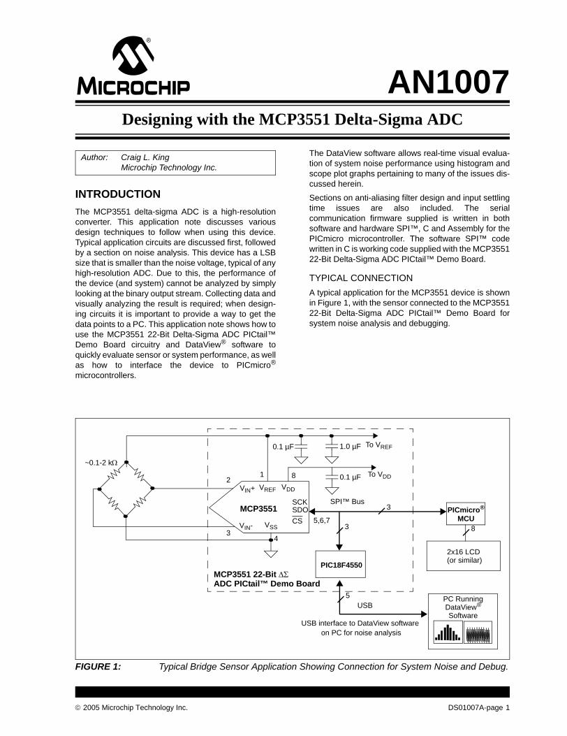
TYPICAL CONNECTIONA typical application for the MCP3551 device is shownin Figure 1, with the sensor connected to the MCP355122-Bit Delta-Sigma ADC PICtail™ Demo Board forsystem noise analysis and debugging.
FIGURE 1: Typical Bridge Sensor Application Showing Connection for System Noise and Debug.
Author: Craig L. KingMicrochip Technology Inc.
USB interface to DataView software
PC Running
SPI™ Bus
on PC for noise analysis
2x16 LCD (or similar)
0.1 µFVIN+
VIN-
VREF
PIC18F4550
VDD
VSS
SCKSDOCS
MCP3551MCU
MCP3551 22-Bit ΔΣ
USB
0.1 µF 1.0 µF To VREF
To VDD
DataView®
5,6,7
12
34
8
3
3
5
8
~0.1-2 kΩ
PICmicro®
Software
ADC PICtail™ Demo Board
Designing with the MCP3551 Delta-Sigma ADC
AN1007
DS01007A-page 2 © 2005 Microchip Technology Inc.
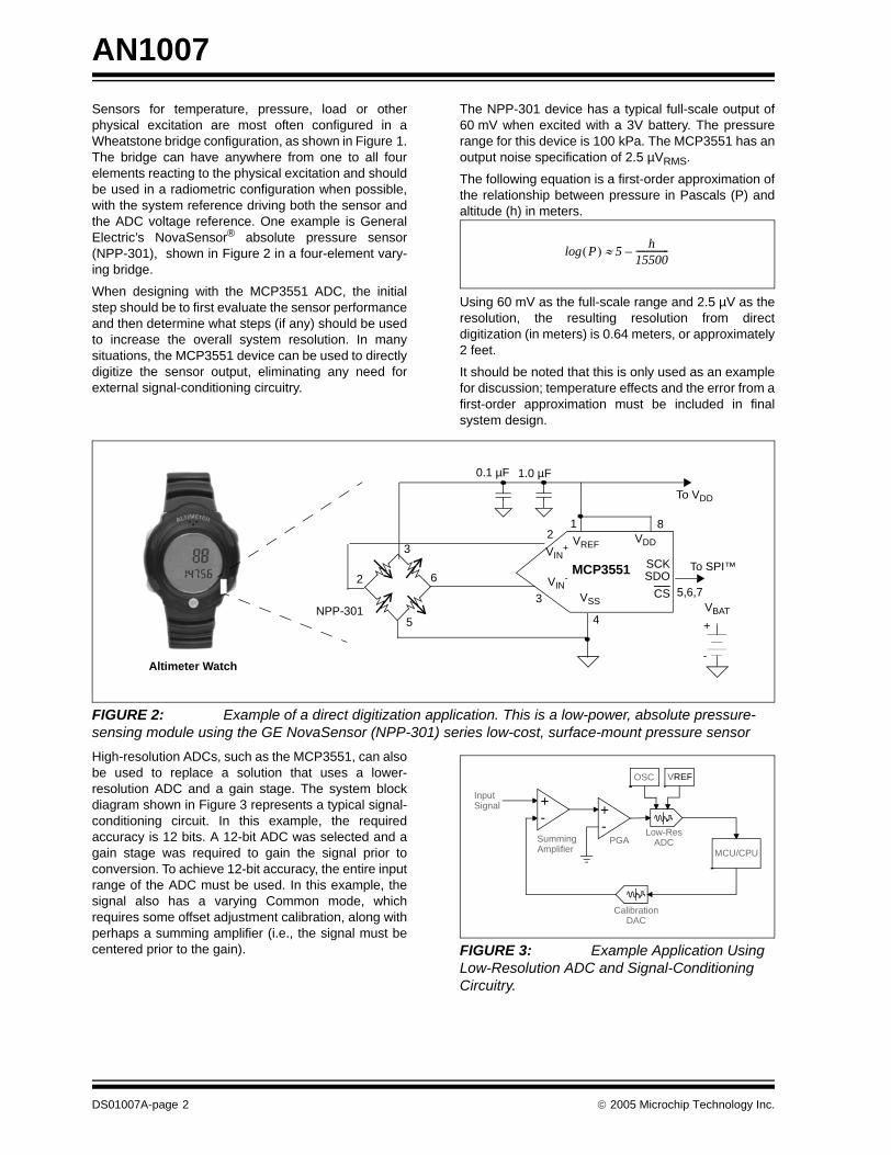
Sensors for temperature, pressure, load or otherphysical excitation are most often configured in aWheatstone bridge configuration, as shown in Figure 1.The bridge can have anywhere from one to all fourelements reacting to the physical excitation and shouldbe used in a radiometric configuration when possible,with the system reference driving both the sensor andthe ADC voltage reference. One example is GeneralElectric’s NovaSensor® absolute pressure sensor(NPP-301), shown in Figure 2 in a four-element vary-ing bridge.
When designing with the MCP3551 ADC, the initialstep should be to first evaluate the sensor performanceand then determine what steps (if any) should be usedto increase the overall system resolution. In manysituations, the MCP3551 device can be used to directlydigitize the sensor output, eliminating any need forexternal signal-conditioning circuitry.
The NPP-301 device has a typical full-scale output of60 mV when excited with a 3V battery. The pressurerange for this device is 100 kPa. The MCP3551 has anoutput noise specification of 2.5 µVRMS.
The following equation is a first-order approximation ofthe relationship between pressure in Pascals (P) andaltitude (h) in meters.
Using 60 mV as the full-scale range and 2.5 µV as theresolution, the resulting resolution from directdigitization (in meters) is 0.64 meters, or approximately2 feet.
It should be noted that this is only used as an examplefor discussion; temperature effects and the error from afirst-order approximation must be included in finalsystem design.
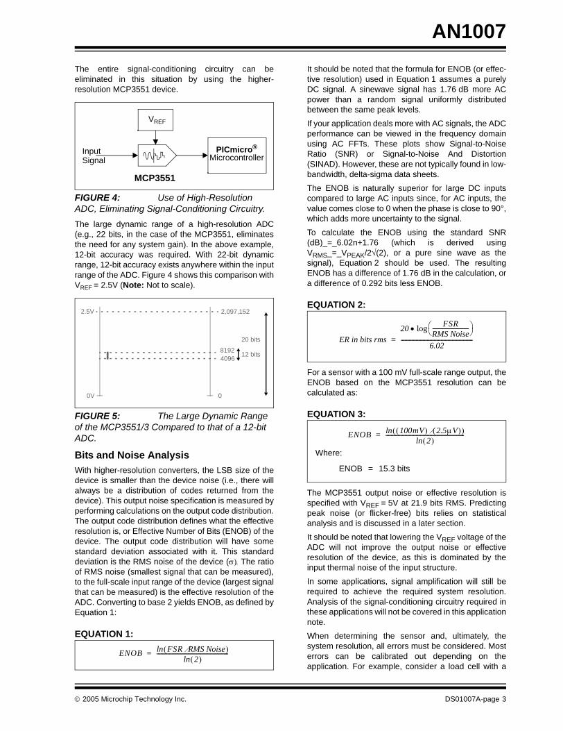
FIGURE 2: Example of a direct digitization application. This is a low-power, absolute pressure-sensing module using the GE NovaSensor (NPP-301) series low-cost, surface-mount pressure sensor High-resolution ADCs, such as the MCP3551, can alsobe used to replace a solution that uses a lower-resolution ADC and a gain stage. The system blockdiagram shown in Figure 3 represents a typical signal-conditioning circuit. In this example, the requiredaccuracy is 12 bits. A 12-bit ADC was selected and again stage was required to gain the signal prior toconversion. To achieve 12-bit accuracy, the entire inputrange of the ADC must be used. In this example, thesignal also has a varying Common mode, whichrequires some offset adjustment calibration, along withperhaps a summing amplifier (i.e., the signal must becentered prior to the gain). FIGURE 3: Example Application Using
Low-Resolution ADC and Signal-Conditioning Circuitry.
P( )log 5 h15500---------------–≈
NPP-301
0.1 µF 1.0 µF
VIN+
VIN-
VREF VDD
VSS
SCKSDO
CS
MCP3551
VBAT
To VDD
To SPI™
+
-
3
2 6
5
2
3
1
4
5,6,7
8
Altimeter Watch
CalibrationDAC
MCU/CPU
Low-ResADCPGASumming
Amplifier
InputSignal
OSC VREF
+-
+-
© 2005 Microchip Technology Inc. DS01007A-page 3
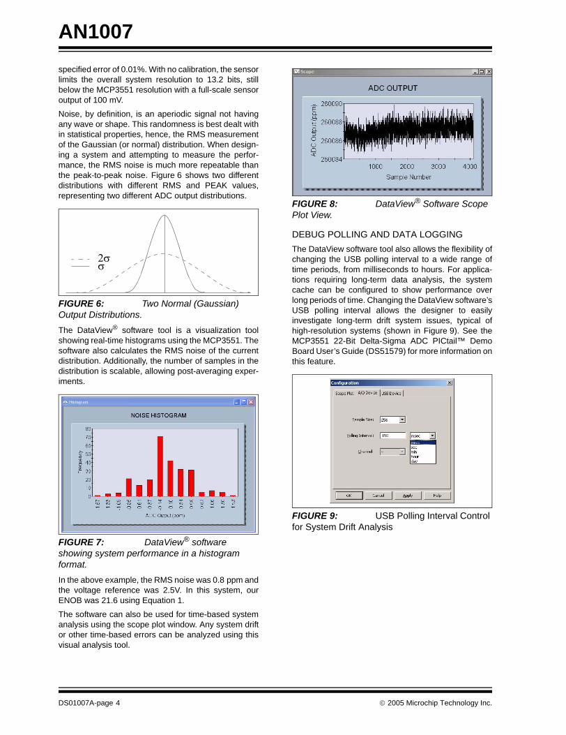
AN1007The entire signal-conditioning circuitry can beeliminated in this situation by using the higher-resolution MCP3551 device.
FIGURE 4: Use of High-Resolution ADC, Eliminating Signal-Conditioning Circuitry.The large dynamic range of a high-resolution ADC(e.g., 22 bits, in the case of the MCP3551, eliminatesthe need for any system gain). In the above example,12-bit accuracy was required. With 22-bit dynamicrange, 12-bit accuracy exists anywhere within the inputrange of the ADC. Figure 4 shows this comparison withVREF = 2.5V (Note: Not to scale).
FIGURE 5: The Large Dynamic Range of the MCP3551/3 Compared to that of a 12-bit ADC.
Bits and Noise AnalysisWith higher-resolution converters, the LSB size of thedevice is smaller than the device noise (i.e., there willalways be a distribution of codes returned from thedevice). This output noise specification is measured byperforming calculations on the output code distribution.The output code distribution defines what the effectiveresolution is, or Effective Number of Bits (ENOB) of thedevice. The output code distribution will have somestandard deviation associated with it. This standarddeviation is the RMS noise of the device (σ). The ratioof RMS noise (smallest signal that can be measured),to the full-scale input range of the device (largest signalthat can be measured) is the effective resolution of theADC. Converting to base 2 yields ENOB, as defined byEquation 1:
EQUATION 1:
It should be noted that the formula for ENOB (or effec-tive resolution) used in Equation 1 assumes a purelyDC signal. A sinewave signal has 1.76 dB more ACpower than a random signal uniformly distributedbetween the same peak levels.
If your application deals more with AC signals, the ADCperformance can be viewed in the frequency domainusing AC FFTs. These plots show Signal-to-NoiseRatio (SNR) or Signal-to-Noise And Distortion(SINAD). However, these are not typically found in low-bandwidth, delta-sigma data sheets.
The ENOB is naturally superior for large DC inputscompared to large AC inputs since, for AC inputs, thevalue comes close to 0 when the phase is close to 90°,which adds more uncertainty to the signal.
To calculate the ENOB using the standard SNR(dB)_=_6.02n+1.76 (which is derived usingVRMS_=_VPEAK/2√(2), or a pure sine wave as thesignal), Equation 2 should be used. The resultingENOB has a difference of 1.76 dB in the calculation, ora difference of 0.292 bits less ENOB.
EQUATION 2:
For a sensor with a 100 mV full-scale range output, theENOB based on the MCP3551 resolution can becalculated as:
EQUATION 3:
The MCP3551 output noise or effective resolution isspecified with VREF = 5V at 21.9 bits RMS. Predictingpeak noise (or flicker-free) bits relies on statisticalanalysis and is discussed in a later section.
It should be noted that lowering the VREF voltage of theADC will not improve the output noise or effectiveresolution of the device, as this is dominated by theinput thermal noise of the input structure.
In some applications, signal amplification will still berequired to achieve the required system resolution.Analysis of the signal-conditioning circuitry required inthese applications will not be covered in this applicationnote.
When determining the sensor and, ultimately, thesystem resolution, all errors must be considered. Mosterrors can be calibrated out depending on theapplication. For example, consider a load cell with a
VREF
PICmicro®Microcontroller
InputSignal
MCP3551
0V
2,097,1522.5V
20 bits
8192 12 bits4096
0
ENOB FSR RMS Noise⁄( )ln2( )ln
----------------------------------------------------=
ER in bits rms20 FSR
RMS Noise--------------------------⎝ ⎠
⎛ ⎞log•
6.02----------------------------------------------------=
ENOB 100mV( ) 2.5μV( )⁄( )ln2( )ln
---------------------------------------------------------=
Where:
ENOB = 15.3 bits
AN1007
DS01007A-page 4 © 2005 Microchip Technology Inc.
specified error of 0.01%. With no calibration, the sensorlimits the overall system resolution to 13.2 bits, stillbelow the MCP3551 resolution with a full-scale sensoroutput of 100 mV.
Noise, by definition, is an aperiodic signal not havingany wave or shape. This randomness is best dealt within statistical properties, hence, the RMS measurementof the Gaussian (or normal) distribution. When design-ing a system and attempting to measure the perfor-mance, the RMS noise is much more repeatable thanthe peak-to-peak noise. Figure 6 shows two differentdistributions with different RMS and PEAK values,representing two different ADC output distributions.
FIGURE 6: Two Normal (Gaussian) Output Distributions.The DataView® software tool is a visualization toolshowing real-time histograms using the MCP3551. Thesoftware also calculates the RMS noise of the currentdistribution. Additionally, the number of samples in thedistribution is scalable, allowing post-averaging exper-iments.
FIGURE 7: DataView® software showing system performance in a histogram format.In the above example, the RMS noise was 0.8 ppm andthe voltage reference was 2.5V. In this system, ourENOB was 21.6 using Equation 1.
The software can also be used for time-based systemanalysis using the scope plot window. Any system driftor other time-based errors can be analyzed using thisvisual analysis tool.
FIGURE 8: DataView® Software Scope Plot View.
DEBUG POLLING AND DATA LOGGINGThe DataView software tool also allows the flexibility ofchanging the USB polling interval to a wide range oftime periods, from milliseconds to hours. For applica-tions requiring long-term data analysis, the systemcache can be configured to show performance overlong periods of time. Changing the DataView software’sUSB polling interval allows the designer to easilyinvestigate long-term drift system issues, typical ofhigh-resolution systems (shown in Figure 9). See theMCP3551 22-Bit Delta-Sigma ADC PICtail™ DemoBoard User’s Guide (DS51579) for more information onthis feature.
FIGURE 9: USB Polling Interval Control for System Drift Analysis
σ2σ
will supply new figure
© 2005 Microchip Technology Inc. DS01007A-page 5
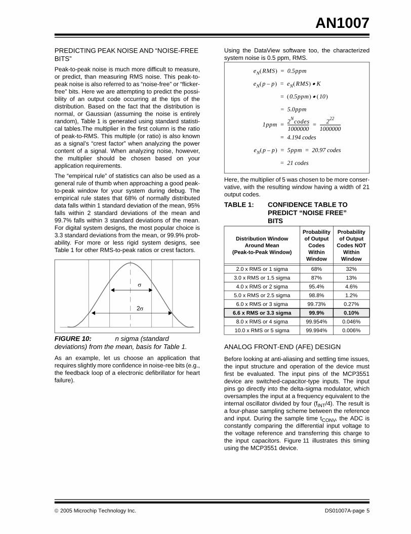
AN1007PREDICTING PEAK NOISE AND “NOISE-FREE BITS”Peak-to-peak noise is much more difficult to measure,or predict, than measuring RMS noise. This peak-to-peak noise is also referred to as “noise-free” or “flicker-free” bits. Here we are attempting to predict the possi-bility of an output code occurring at the tips of thedistribution. Based on the fact that the distribution isnormal, or Gaussian (assuming the noise is entirelyrandom), Table 1 is generated using standard statisti-cal tables.The multiplier in the first column is the ratioof peak-to-RMS. This multiple (or ratio) is also knownas a signal’s “crest factor” when analyzing the powercontent of a signal. When analyzing noise, however,the multiplier should be chosen based on yourapplication requirements.
The “empirical rule” of statistics can also be used as ageneral rule of thumb when approaching a good peak-to-peak window for your system during debug. Theempirical rule states that 68% of normally distributeddata falls within 1 standard deviation of the mean, 95%falls within 2 standard deviations of the mean and99.7% falls within 3 standard deviations of the mean.For digital system designs, the most popular choice is3.3 standard deviations from the mean, or 99.9% prob-ability. For more or less rigid system designs, seeTable 1 for other RMS-to-peak ratios or crest factors.
FIGURE 10: n sigma (standard deviations) from the mean, basis for Table 1.As an example, let us choose an application thatrequires slightly more confidence in noise-ree bits (e.g.,the feedback loop of a electronic defibrillator for heartfailure).
Using the DataView software too, the characterizedsystem noise is 0.5 ppm, RMS.
Here, the multiplier of 5 was chosen to be more conser-vative, with the resulting window having a width of 21output codes.
TABLE 1: CONFIDENCE TABLE TO PREDICT “NOISE FREE” BITS
ANALOG FRONT-END (AFE) DESIGN
Before looking at anti-aliasing and settling time issues,the input structure and operation of the device mustfirst be evaluated. The input pins of the MCP3551device are switched-capacitor-type inputs. The inputpins go directly into the delta-sigma modulator, whichoversamples the input at a frequency equivalent to theinternal oscillator divided by four (fINT/4). The result isa four-phase sampling scheme between the referenceand input. During the sample time tCONV, the ADC isconstantly comparing the differential input voltage tothe voltage reference and transferring this charge tothe input capacitors. Figure 11 illustrates this timingusing the MCP3551 device.
σ
2σ
Distribution Window Around Mean
(Peak-to-Peak Window)
Probability of Output
Codes Within
Window
Probability of Output
Codes NOT Within
Window
2.0 x RMS or 1 sigma 68% 32%3.0 x RMS or 1.5 sigma 87% 13%4.0 x RMS or 2 sigma 95.4% 4.6%
5.0 x RMS or 2.5 sigma 98.8% 1.2%6.0 x RMS or 3 sigma 99.73% 0.27%
6.6 x RMS or 3.3 sigma 99.9% 0.10%8.0 x RMS or 4 sigma 99.954% 0.046%
10.0 x RMS or 5 sigma 99.994% 0.006%
eN RMS( ) 0.5ppm=
eN p p–( ) eN RMS( ) K•=
0.5ppm( ) 10( )•=
5.0ppm=
1ppm 2Ncodes1000000--------------------- 222
1000000---------------------= =
4.194 codes=
eN p p–( ) 5ppm 20.97 codes= =
21 codes=

AN1007
DS01007A-page 6 © 2005 Microchip Technology Inc.
FIGURE 11: Internal timings of the MCP3551 device. For settling time issues, charge transfer frequency must be observed. For aliasing issues, the oversampling frequency of 28.16 kHz is the focus.
ANTI-ALIASING FILTER DESIGNRegardless of the ADC architecture, an anti-aliasingfilter is sometimes required. The delta-sigma ADC is noexception. Based on the SINC filter response inFigure 12, a simple, low-cost RC filter is all that isrequired to eliminate unwanted signals around theoversampling frequency.
The MCP3551 device has an oversampling frequencyof 28.16 kHz. The MCP3553 device has anoversampling frequency of 30.72 kHz, with a lowerOversampling Ratio (OSR) for higher data rate orNyquist frequency. The Nyquist or output data rate ofthe MCP3551 and MCP3553 devices are 13.75 Hz and60 Hz, respectively.
The SINC filter response of the MCP3551 has lobesthat give increasing attenuation with frequency, asshown in Figure 12. The anti-aliasing filter require-ments should be selected with the attenuation of theSINC filter in mind.
FIGURE 12: MCP3551's modified SINC filter.Keep in mind that the ill-used components will not be atfull-scale, and will typically be at a smaller amplitude.From Figure 12, the largest SINC lobe is down approx-imately 60 dB (the aliasing components are at -20 dB),so an additional 20 dB is required from the anti-lasingfilter to get to 100 dB.
Microchip’s free FilterLab® filter design tool can beused to easily estimate the single-pole RC attenuationfor specific filter cut-off frequencies and aliased signalfrequency components. Figure 13 shows a RCdesigned with a 1 kHz cut-off frequency, giving greaterthan 30 dB at the sampling frequency of 30.72 kHz.
It should be noted that at integer multiples of thesampling frequency, the SINC filter response willrepeat, in which the SINC filter response will be zero.
FIGURE 13: FilterLab® filter design tool showing RC response.
INPUT IMPEDANCEIn Figure 11, the switching frequency at the inputs ofthe devices is equivalent to the internal oscillatorfrequency in every phase. The input pin resistance iscalculated to be the switching frequency multiplied bythe capacitance and the equivalent capacitance (CEQ).The resulting RC defines the settling time required atthe input to the device.
Any additional RC added to the input will cause theinput signal to not be completely settled during theoversampling internal to the device. It is important tonote that, due to the oversampling and averagingperformed by the delta-sigma architecture, the addi-tional RC added here will be consistent across eachoversampled charge. The resulting effect on the deviceoutput will be an error in conversion offset and gain.
tDATA = 72.72 ms
Filter Order 1 Filter Order 2 Filter Order 3 Filter Order 4
X 51228.16 kHz
112.64 kHz 112.64 kHz 112.64 kHz 112.64 kHzTransfer ChargeSample Input
X 512X 512
Transfer ChargeSample Reference
X 512
-120-110-100-90-80-70-60-50-40-30-20-10
0
0 10 20 30 40 50 60 70 80 90 100 110Frequency (Hz)
Atte
nuat
ion
(dB
)
© 2005 Microchip Technology Inc. DS01007A-page 7
AN1007The linearity of the device will not be compromised.The output noise performance will also not be compro-mised, assuming the thermal noise added by the inputresistance does not exceed the output noise specifica-tion
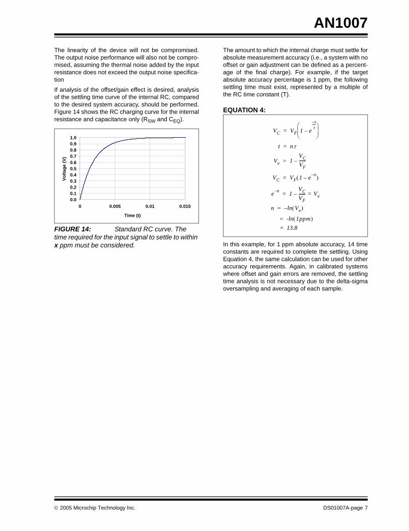
If analysis of the offset/gain effect is desired, analysisof the settling time curve of the internal RC, comparedto the desired system accuracy, should be performed.Figure 14 shows the RC charging curve for the internalresistance and capacitance only (RSW and CEQ).
FIGURE 14: Standard RC curve. The time required for the input signal to settle to within x ppm must be considered.
The amount to which the internal charge must settle forabsolute measurement accuracy (i.e., a system with nooffset or gain adjustment can be defined as a percent-age of the final charge). For example, if the targetabsolute accuracy percentage is 1 ppm, the followingsettling time must exist, represented by a multiple ofthe RC time constant (T).
EQUATION 4:
In this example, for 1 ppm absolute accuracy, 14 timeconstants are required to complete the settling. UsingEquation 4, the same calculation can be used for otheraccuracy requirements. Again, in calibrated systemswhere offset and gain errors are removed, the settlingtime analysis is not necessary due to the delta-sigmaoversampling and averaging of each sample.
0.00.10.20.30.40.50.60.70.80.91.0
0 0.005 0.01 0.015
Time (t)
Volta
ge (V
)
VC VF 1 et–
τ----
–⎝ ⎠⎜ ⎟⎛ ⎞
=
t nτ=
Ve 1VCVF-------–=
VC VF 1 e n––( )=
e n– 1VCVF------- Ve=–=
n ln– Ve( )=
-ln 1ppm( )=13.8=

AN1007
DS01007A-page 8 © 2005 Microchip Technology Inc.
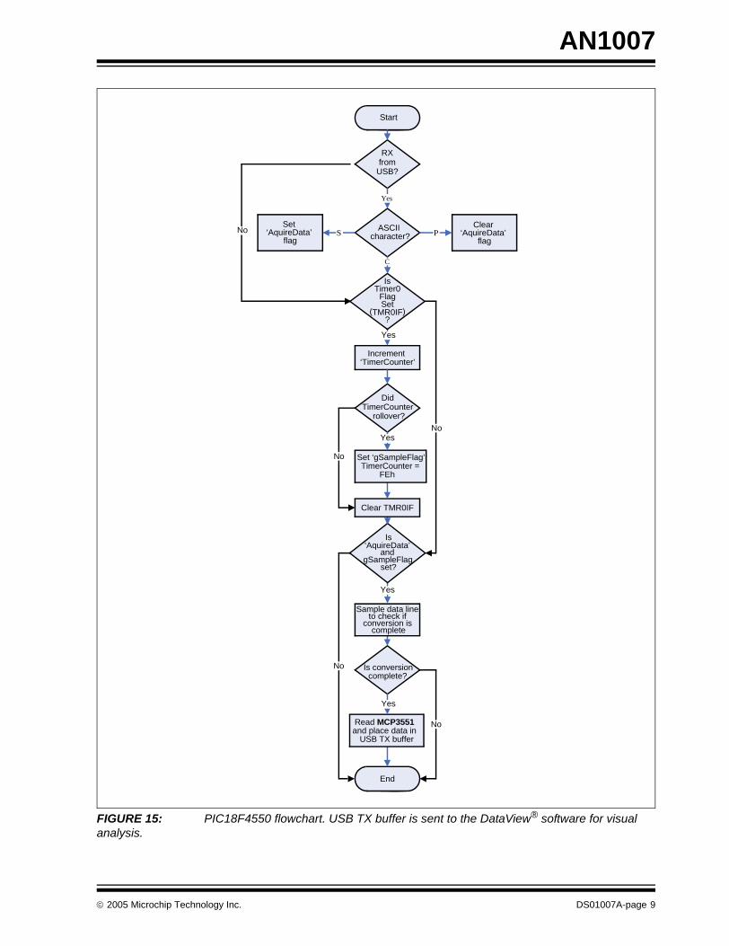
Communication FirmwareThe MCP3551 ADCs are serial SPI™ devices. Thisapplication note includes code written in both C andassembly languages. The MCP3551 22-Bit Delta-Sigma ADC PICtail™ Demo Board connects with theDataView software through the PIC18F4550 via USBand is supplied with code written using Microchip’s C18compiler. An overview of the SPI communicationprotocol used is shown here:
As long as the system has been put into the AcquireData mode from the DataView software (by sending anASCII “S” via USB to the PIC18F4550), the Acquire-Data flag will be set. During this time, the MCP3551 isconstantly converting, with the read data being sentback up to the PC via USB.
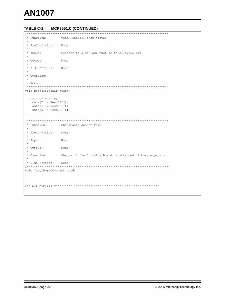
The code used on the PIC18F4550 sends CS lowpulses to the MCP3551 every 10 ms. The Timer1 flagand the TimerCounter variable are used to set thistime. This low pulse effectively puts the device intoSingle Conversion mode, as the rising edge is less thanthe conversion time. During the CS pulse low time, thestate of the SDO is tested to determine if the conver-sion is complete. If the pin is low, the firmware willretrieve the data using the Read3551 subroutine. TheRead3551() routine calls three separate ReadSPIroutines and retrieves the three bytes of data contain-ing the 22-bit word and the 2 overflow bits. Once the 3bytes of data are returned, the Sample flag is reset andthe process starts over.
void Read3551(char *data){ unsigned char n; data[2] = ReadSPI(); data[1] = ReadSPI(); data[0] = ReadSPI(); }
//MCU checks every 10 ms if conversion is finished if(AquireData & gSampleFlag) { CS_PTBoard_LOW(); // for(n=0;n<5;n++); if (SDIpin == 0) Read3551(outbuffer); CS_PTBoard_HIGH(); // gSampleFlag = 0; //clear timeout indicator
if(!mHIDTxIsBusy()) HIDTxReport(outbuffer,3); }
© 2005 Microchip Technology Inc. DS01007A-page 9
AN1007
FIGURE 15: PIC18F4550 flowchart. USB TX buffer is sent to the DataView® software for visual analysis.
Start
RX
Clear
flagASCII
character?
Increment ‘TimerCounter’
Did TimerCounter
rollover?
Set ‘gSampleFlag’TimerCounter =
FEh
Is
and gSampleFlag
set?
Sample data line to check if
conversion is complete
Is conversion complete?
Read MCP3551 and place data in
USB TX buffer
No
Clear TMR0IF
PS
C
No
Yes
Yes
No
Yes
End
No
Yes
No
Yes
fromUSB?
‘AquireData’ Set
flag‘AquireData’
Is
Set Flag
(TMR0IF)
Timer0
?
‘AquireData’
AN1007
DS01007A-page 10 © 2005 Microchip Technology Inc.
REFERENCES[1] “Delta-Sigma Data Converters Theory, Design and
Simulation”, Steven R. Norsworthy, RichardSchreier, Gabor C. Temes, IEEE Press, 1997, pp. 4-9.
[2] AN9504, “A Brief Introduction to Sigma DeltaConversion”, David Jarman, Intersil®, 1995.
[3] “Modern Business Statistics”, Ronald L. Iman, W.J.Conover, Second Edition, John Wiley & Sons, Inc.,1989.
APPENDIX A: OVERSAMPLING ANALYSIS
The delta-sigma ADC is an oversampling device withmany up-sides. High resolution, excellent linefrequency rejection, limited external componentrequirements and low power are a few examples of itsbenefits. The high-resolution benefit is not a product ofsimple oversampling, which is sometimes confused.
WHY NOT JUST OVERSAMPLE WITH A PICmicro® MCU SAR ADC?The answer is easy: noise shaping. Simply oversam-pling with a fast Successive Approximation Routine(SAR) ADC and averaging the results will not achievethe resolution performance of a delta-sigma ADC.Oversampling and averaging will only increaseaccuracy by 1/2 bit for each doubling of the samplefrequency. The theory behind this comparison ispresented here by comparing the noise power of bothapproaches.
SIMPLE OVERSAMPLINGFor a generic quanitized unit (or LSB), the noise withinthis quanta is assumed to be entirely random, orassumed to be white-noise. Therefore, the quantizationnoise power and RMS quantization voltage for andigital or quantized output (ADC) can be given by thefollowing equations:
EQUATION 5:
For example, for a 16-bit converter with a VREF of 5V,the RMS quantization noise would be 22 µV.
Taking this noise and folding it into the frequency bandfrom 0 to fs/2, due to Nyquist, we can determine whatthe spectral density of the noise is in V/√(Hz):
EQUATION 6:
To determine the noise power within a bandwidth ofinterest (fo), we must now square, and then integrate,the noise over that bandwidth of interest.
e2rms 1q--- e2deq–
2------
q2---
∫ q2
12------= =
rmse q12
----------= (V)
(V2)
E f( ) rmse( ) 2fs---= V
Hz-----------⎝ ⎠
⎛ ⎞

© 2005 Microchip Technology Inc. DS01007A-page 11
AN1007EQUATION 7:
Recalling that fs/2fo is the OSR, we now have the wellestablished result that increasing the OSR reduced thenoise by the square root of the OSR [1]. Therefore,each doubling of the sampling frequency only yields3 dB better performance, or only 0.5 bits of resolution.
The delta-sigma modulator will increase the perfor-mance of oversampling by pushing the low-frequencynoise towards the higher frequencies, see Figure 17.This benefit of delta-sigma modulation is referred to asnoise shaping. A first-order delta-sigma modulator willincrease accuracy by 9 dB, or 1.5 bits of resolution, forevery doubling of the OSR.
The output of the accumulator is the input signal plusthe error introduced by the quanitzation error, as wellas the quantized signal, represented by the followingfigure and equation:
FIGURE 16: Representation of a first-order delta-sigma modulator in its sampled-data equivalent form [1].
EQUATION 8:
Taking spectral density of the noise (ei-ei-1) and thenagain converting this to noise power by squaring it andintegrating it over the bandwidth of interest eventuallyyields:
EQUATION 9:
The delta-sigma modulator decreases in-band noise by9 dB (or 1.5 bits) for every doubling of the OSR. Threetimes better than simple oversampling.
Improving noise-shaping performance can be achievedusing a higher-order delta-sigma modulator design.The noise power for higher-order modulators issummarized with the following equation:
EQUATION 10:
In this case, the noise falls 3 (2M - 1) dB for everydoubling of the sampling frequency for an Mth-ordermodulator. As an example, for M = 3 (MCP3551/3devices are third-order modulators), for each doublingof the sampling frequency we have an increase in 2.5bits of resolution. It is this architecture that allows< 3 µV of noise performance using devices such as theMCP3551/3. Figure 17 presents the noise-shaping inthe frequency domain. The noise has been pushed tothe higher frequencies, around the oversamplingfrequency (fs). It should also be noted that thermalnoise follows the standard averaging rule of 3 dB (1/2bit) improvement with every doubling of the OSR, as itis taken and processed as part of the signal.
FIGURE 17: Noise-shaping from a delta-sigma modulator achieving lower noise floor in the bandwidth of interest. This is not possible by simply oversampling and averaging with a faster SAR ADC.
no2 e f( )( )= V2( )
no erms( )2fofs
-------⎝ ⎠⎛ ⎞
1 2/= V( )
Where:
fo < fs/2
Delay+-
QuantizationAccumulationxi yi
ei
+
yi xi 1– ei ei 1––( )+=
no eRMSπ3
-------2fofs
-------⎝ ⎠⎛ ⎞
32---
=
no eRMSπM
2M 1+---------------------
2fofs
-------⎝ ⎠⎛ ⎞
M 12---+
=
0 f0
DigitalFilter
2f0Nyquist
fsOversampling
frequency
Mag
nitu
de STF
AN1007
DS01007A-page 12 © 2005 Microchip Technology Inc.
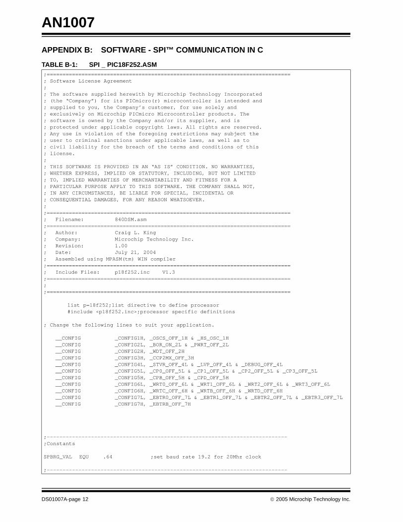
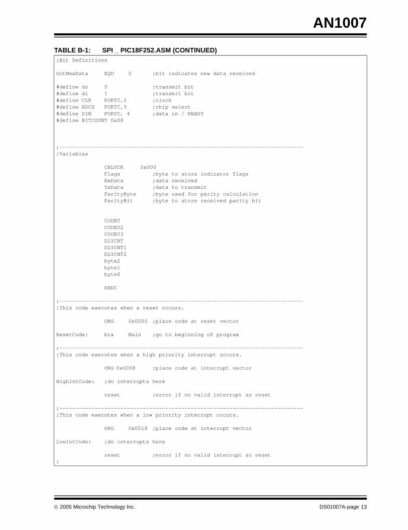
APPENDIX B: SOFTWARE - SPI™ COMMUNICATION IN C
TABLE B-1: SPI _ PIC18F252.ASM;=============================================================================; Software License Agreement;; The software supplied herewith by Microchip Technology Incorporated ; (the “Company”) for its PICmicro(r) microcontroller is intended and ; supplied to you, the Company’s customer, for use solely and ; exclusively on Microchip PICmicro Microcontroller products. The ; software is owned by the Company and/or its supplier, and is ; protected under applicable copyright laws. All rights are reserved. ; Any use in violation of the foregoing restrictions may subject the ; user to criminal sanctions under applicable laws, as well as to ; civil liability for the breach of the terms and conditions of this ; license.;; THIS SOFTWARE IS PROVIDED IN AN “AS IS” CONDITION. NO WARRANTIES, ; WHETHER EXPRESS, IMPLIED OR STATUTORY, INCLUDING, BUT NOT LIMITED ; TO, IMPLIED WARRANTIES OF MERCHANTABILITY AND FITNESS FOR A ; PARTICULAR PURPOSE APPLY TO THIS SOFTWARE. THE COMPANY SHALL NOT, ; IN ANY CIRCUMSTANCES, BE LIABLE FOR SPECIAL, INCIDENTAL OR ; CONSEQUENTIAL DAMAGES, FOR ANY REASON WHATSOEVER.;;=============================================================================; Filename: 840DSM.asm;=============================================================================; Author: Craig L. King; Company: Microchip Technology Inc.; Revision: 1.00; Date: July 21, 2004; Assembled using MPASM(tm) WIN compiler ;=============================================================================; Include Files: p18f252.inc V1.3;=============================================================================;;=============================================================================
list p=18f252;list directive to define processor#include <p18f252.inc>;processor specific definitions
; Change the following lines to suit your application.
__CONFIG _CONFIG1H, _OSCS_OFF_1H & _HS_OSC_1H__CONFIG _CONFIG2L, _BOR_ON_2L & _PWRT_OFF_2L__CONFIG _CONFIG2H, _WDT_OFF_2H__CONFIG _CONFIG3H, _CCP2MX_OFF_3H__CONFIG _CONFIG4L, _STVR_OFF_4L & _LVP_OFF_4L & _DEBUG_OFF_4L__CONFIG _CONFIG5L, _CP0_OFF_5L & _CP1_OFF_5L & _CP2_OFF_5L & _CP3_OFF_5L __CONFIG _CONFIG5H, _CPB_OFF_5H & _CPD_OFF_5H__CONFIG _CONFIG6L, _WRT0_OFF_6L & _WRT1_OFF_6L & _WRT2_OFF_6L & _WRT3_OFF_6L __CONFIG _CONFIG6H, _WRTC_OFF_6H & _WRTB_OFF_6H & _WRTD_OFF_6H__CONFIG _CONFIG7L, _EBTR0_OFF_7L & _EBTR1_OFF_7L & _EBTR2_OFF_7L & _EBTR3_OFF_7L__CONFIG _CONFIG7H, _EBTRB_OFF_7H
;----------------------------------------------------------------------------;Constants
SPBRG_VAL EQU .64 ;set baud rate 19.2 for 20Mhz clock
;----------------------------------------------------------------------------
© 2005 Microchip Technology Inc. DS01007A-page 13
AN1007
;Bit Definitions
GotNewData EQU 0 ;bit indicates new data received
#define do 0 ;transmit bit#define di 1 ;transmit bit#define CLK PORTC,2 ;clock#define ADCS PORTC,3 ;chip select#define DIN PORTC, 4 ;data in / READY#define BITCOUNT 0x08
;----------------------------------------------------------------------------;Variables
CBLOCK 0x000Flags ;byte to store indicator flagsRxData ;data receivedTxData ;data to transmitParityByte ;byte used for parity calculationParityBit ;byte to store received parity bit
COUNTCOUNT2COUNT3DLYCNTDLYCNT1DLYCNT2byte2byte1byte0
ENDC
;----------------------------------------------------------------------------;This code executes when a reset occurs.
ORG 0x0000 ;place code at reset vector
ResetCode: bra Main ;go to beginning of program
;----------------------------------------------------------------------------;This code executes when a high priority interrupt occurs.
ORG 0x0008 ;place code at interrupt vector
HighIntCode: ;do interrupts here
reset ;error if no valid interrupt so reset
;----------------------------------------------------------------------------;This code executes when a low priority interrupt occurs.
ORG 0x0018 ;place code at interrupt vector
LowIntCode: ;do interrupts here
reset ;error if no valid interrupt so reset;
TABLE B-1: SPI _ PIC18F252.ASM (CONTINUED)
AN1007
DS01007A-page 14 © 2005 Microchip Technology Inc.
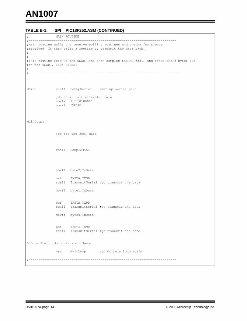
; MAIN ROUTINE;----------------------------------------------------------------------------;Main routine calls the receive polling routines and checks for a byte;received. It then calls a routine to transmit the data back.;;;This routine sets up the USART and then samples the MCP3551, and sends the 3 bytes out;on the USART, THEN REPEAT;;------------------------------------------------------------------------------
Main: rcall SetupSerial ;set up serial port
;do other initialization heremovlw b’11010000’movwf TRISC
MainLoop:
;go get the 3551 data
rcall Sample3551
movff byte2,TxData
bsf TXSTA,TX9Drcall TransmitSerial ;go transmit the data
movff byte1,TxData
bcf TXSTA,TX9Drcall TransmitSerial ;go transmit the data
movff byte0,TxData
bcf TXSTA,TX9Drcall TransmitSerial ;go transmit the data
DoOtherStuff:;do other stuff here
bra MainLoop ;go do main loop again
;----------------------------------------------------------------------------
TABLE B-1: SPI _ PIC18F252.ASM (CONTINUED)

© 2005 Microchip Technology Inc. DS01007A-page 15
AN1007
;Check if data received and if so, place in a register and check parity.
ReceiveSerial: btfss PIR1,RCIF ;check if data receivedreturn ;return if no data
btfsc RCSTA,OERR ;if overrun error occurredbra ErrSerialOverr ;then go handle errorbtfsc RCSTA,FERR ;if framing error occurredbra ErrSerialFrame ;then go handle error
movf RCSTA,W ;get received parity bitmovwf ParityBit ;and savemovf RCREG,W ;get received datamovwf RxData ;and save
rcall CalcParity ;calculate paritymovf ParityBit,W ;get received parity bitxorwf ParityByte,F ;compare with calculated parity bitbtfsc ParityByte,0 ;check result of comparisonbra ErrSerlParity ;if parity is different, then errorbsf Flags,GotNewData ;else indicate new data receivedreturn
;error because OERR overrun error bit is set;can do special error handling here - this code simply clears and continues
ErrSerialOverr:bcf RCSTA,CREN ;reset the receiver logicbsf RCSTA,CREN ;enable reception againreturn
;error because FERR framing error bit is set;can do special error handling here - this code simply clears and continues
ErrSerialFrame:movf RCREG,W ;discard received data that has errorreturn
;error because parity bit is not correct;can do special error handling here - this code simply clears and continues
ErrSerlParity: return ;return without indicating new data
;----------------------------------------------------------------------------;Transmit data in WREG with parity when the transmit register is empty.
TransmitSerial:btfss PIR1,TXIF ;check if transmitter busybra $-2 ;wait until transmitter is not busy
movf TxData,W ;get data to be transmitted
movf TxData,W ;get data to transmitmovwf TXREG ;transmit the datareturn
;----------------------------------------------------------------------------
TABLE B-1: SPI _ PIC18F252.ASM (CONTINUED)
AN1007
DS01007A-page 16 © 2005 Microchip Technology Inc.
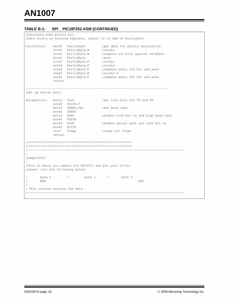
;Calculate even parity bit.;Data starts in working register, result is in LSB of ParityByte
CalcParity: movwf ParityByte ;get data for parity calculationrrncf ParityByte,W ;rotatexorwf ParityByte,W ;compare all bits against neighbormovwf ParityByte ;saverrncf ParityByte,F ;rotaterrncf ParityByte,F ;rotatexorwf ParityByte,F ;compare every 2nd bit and saveswapf ParityByte,W ;rotate 4xorwf ParityByte,F ;compare every 4th bit and savereturn
;----------------------------------------------------------------------------;Set up serial port.
SetupSerial: movlw 0xc0 ;set tris bits for TX and RXiorwf TRISC,Fmovlw SPBRG_VAL ;set baud ratemovwf SPBRGmovlw 0x64 ;enable nine bit tx and high baud ratemovwf TXSTAmovlw 0xd0 ;enable serial port and nine bit rxmovwf RCSTAclrf Flags ;clear all flagsreturn
;*********************************************************;*********************************************************;-------------------------------------------------------------------------------------;;Sample3551;;This is where you sample the MCP3551 and put your 22-bit;answer into the following bytes:
; byte 2 -- byte 1 -- byte 0; MSB LSB;; This routine returns the data;-------------------------------------------------------------------------------------
TABLE B-1: SPI _ PIC18F252.ASM (CONTINUED)

© 2005 Microchip Technology Inc. DS01007A-page 17
AN1007
Sample3551
clrf byte2 ; reset input bufferclrf byte1 ; reset input bufferclrf byte0 ; reset input buffer
bsf CLK ; clock idle highbcf ADCS ;INITIATE THE CONVERSION
movlw .6call VAR1000TcyDELAY ; delay 1ms
bsf ADCS ;CS HIGH (Single Conversion mode)
movlw .160 ; total delay 110ms (GREATER THAN TCONV, CAN BE REDUCED)call VAR1000TcyDELAY ; delay 160k Tcycall VAR1000TcyDELAY ; delay 250k Tcycall VAR1000TcyDELAY ; delay 250k Tcy
bcf ADCS ; GET THE CONVERSION DATA
movlw BITCOUNTmovwf COUNT ; FIRST BYTE
FIRST_BYTEbcf CLK ; drop clock for next bitbsf CLK ; set clock to latch bitbcf STATUS,C ; pre-clear carrybtfsc DIN ; check for high or low bitbsf STATUS,C ; set carry bitrlcf byte2, f ; roll the carry bit left into positiondecfsz COUNT, f ; decrement bit countergoto FIRST_BYTE ; get next bit
movlw BITCOUNTmovwf COUNT ; SECOND BYTE
SECOND_BYTEbcf CLK ; drop clock for next bitbsf CLK ; set clock to latch bitbcf STATUS,C ; pre-clear carrybtfsc DIN ; check for high or low bitbsf STATUS,C ; set carry bitrlcf byte1, f ; roll the carry bit left into placedecfsz COUNT, f ; decrement bit countergoto SECOND_BYTE ; get next bitmovlw BITCOUNTmovwf COUNT ; THIRD BYTE
THIRD_BYTEbcf CLK ; drop clock for next bitbsf CLK ; set clock to latch bitbcf STATUS,C ; pre-clear carrybtfsc DIN ; check for high or low bitbsf STATUS,C ; set carry bitrlcf byte0, f ; roll the carry bit left into placedecfsz COUNT, f ; decrement bit countergoto THIRD_BYTE ; get next bitbsf CLK ;clock idles high
TABLE B-1: SPI _ PIC18F252.ASM (CONTINUED)
AN1007
DS01007A-page 18 © 2005 Microchip Technology Inc.
bsf ADCS ;deselect A/D converterretlw 0 ; We’re finished - Return!
;******************* VARIABLE DELAY SUBROUTINES *******************; DLYCNT1 = F9h = 249d DLYCNT2 = W; DELAY = T((4 DLYCNT1 + 4) DLYCNT2 + 4);; ex. To create a 300ms delay when using a 4Mhz osc, 300-250 = 50; movlw .50 ;load .50 into WREG; call VAR1000TcyDELAY ;call VAR1000TcyDELAY = 50ms delay w/4MHz Osc; call VAR1000TcyDELAY ;call VAR1000TcyDELAY = 250ms delay w/4MHz Osc; ;total = 300ms delay;************; The value in W at the time of the CALL = x. Delay = 1000Tcy*xVAR1000TcyDELAY
movwf DLYCNT2 ;LOADS CONTROLLING DLY # INTO PRIMARY COUNTERDLOOP2 movlw .249 ;MAXIMIZES THE SECONDARY DLY COUNTER
movwf DLYCNT1 ;DLOOP1 clrwdt ;or NOP
decfsz DLYCNT1,f ; DECREMENT AND TEST SECONDARY LOOP FOR ZEROgoto DLOOP1 ; CONTINUE SECONDARY LOOPdecfsz DLYCNT2,f ; DECREMENT AND TEST PRIMARY DLY COUNTERgoto DLOOP2 ; CONTINUE PRIMARY LOOPretlw .250 ; preload W for the next CALL VAR1000TcyDELAY
;************; VARIABLE 5 Tcy DELAY UP TO 256*5Tcy+5Tcy; DLYCNT1 = W; DELAY = T(1 + 5 DLYCNT1 - 1) + CALL + RETLW;; ex. To create a 250us delay, (250/5)-1 = 49; movlw .49 ;load .49 into WREG; call VAR5TcyDELAY ; call VAR5TcyDELAY;************; The value in W at the time of the CALL = x. Delay = 5*Tcy + 5TcyVAR5TcyDELAY
movwf DLYCNT1 ; LOADS CONTROLLING DLY # INTO PRIMARY COUNTERDLOOP3 clrwdt ;or NOP
nopdecfsz DLYCNT1,f ; DECREMENT AND TEST ZEROgoto DLOOP3 ; CONTINUE LOOPretlw .250 ; preload W for the next CALL VAR5TcyDELAY
;******************************************************************************
HEND
TABLE B-1: SPI _ PIC18F252.ASM (CONTINUED)
© 2005 Microchip Technology Inc. DS01007A-page 19
AN1007
APPENDIX C: HARDWARE - SPI™ COMMUNICATION IN ASSEMBLYTABLE C-1: MCP3551.C/********************************************************************* * * Microchip USB C18 Firmware - MCP3551 PICtail(tm) Demo * ********************************************************************* * FileName: MCP3551.c * Dependencies: See INCLUDES section below * Processor: PIC18 * Compiler: C18 2.30.01+ * Company: Microchip Technology Inc. * * Software License Agreement * * The software supplied herewith by Microchip Technology Incorporated * (the Company) for its PICmicro(r) microcontroller is intended and * supplied to you, the Company’s customer, for use solely and * exclusively on Microchip PICmicro(r) microcontroller products. The * software is owned by the Company and/or its supplier, and is * protected under applicable copyright laws. All rights are reserved. * Any use in violation of the foregoing restrictions may subject the * user to criminal sanctions under applicable laws, as well as to * civil liability for the breach of the terms and conditions of this * license. * * THIS SOFTWARE IS PROVIDED IN AN ”AS IS” CONDITION. NO WARRANTIES, * WHETHER EXPRESS, IMPLIED OR STATUTORY, INCLUDING, BUT NOT LIMITED * TO, IMPLIED WARRANTIES OF MERCHANTABILITY AND FITNESS FOR A * PARTICULAR PURPOSE APPLY TO THIS SOFTWARE. THE COMPANY SHALL NOT, * IN ANY CIRCUMSTANCES, BE LIABLE FOR SPECIAL, INCIDENTAL OR * CONSEQUENTIAL DAMAGES, FOR ANY REASON WHATSOEVER. * * Author Date Comment *~~~~~~~~~~~~~~~~~~~~~~~~~~~~~~~~~~~~~~~~~~~~~~~~~~~~~~~~~~~~~~~~~~~~ * Pat Richards xx/xx/xx Original. ********************************************************************/
/** I N C L U D E S **********************************************************/#include <p18cxxx.h>#include <usart.h>#include <spi.h>#include "system\typedefs.h"#include "system\usb\usb.h"
#include "io_cfg.h" // I/O pin mapping#include "user\MCP3551.h"
/** V A R I A B L E S ********************************************************/#pragma udata//byte old_sw2,old_sw3;
BOOL emulate_mode;rom signed char dir_table[]={-4,-4,-4, 0, 4, 4, 4, 0};byte movement_length;byte vector = 0;
byte AquireData = 1; //0 = STOP; 1 = Aquire char buffer[3];
char inbuffer[BUF_SIZE]; // 8 byte input to USB device bufferchar outbuffer[BUF_SIZE]; // 8 byte output to USB device bufferbyte TimerCounter = 0xF0;static unsigned char gSampleFlag;
AN1007
DS01007A-page 20 © 2005 Microchip Technology Inc.
/** P R I V A T E P R O T O T Y P E S ***************************************/void Read3551(char *data);unsigned char ReadSPI( void );void CheckBoardConnect(void);
/** D E C L A R A T I O N S **************************************************/#pragma codevoid UserInit(void){ byte i; CS_PTBoard_HIGH(); //Drive high tris_CS = 0; //Output
OpenSPI(SPI_FOSC_16, MODE_11, SMPMID); TRISBbits.TRISB0 = 1; //SDI TRISBbits.TRISB1 = 0; //SCK
//------------------------- // initialize variables //------------------------- for (i=0; i<BUF_SIZE; i++) // initialize input and output buffer to 0 { inbuffer[i]=0; outbuffer[i]=0; }
//Timer 0 TMR0H = 0; //clear timer TMR0L = 0; //clear timer
T0CONbits.PSA = 0; //Assign prescaler to Timer 0T0CONbits.T0PS2 = 1; //Setup prescalerT0CONbits.T0PS1 = 1; //Will time out every 51 us based onT0CONbits.T0PS0 = 1; //20 MHz FoscT0CONbits.T0CS = 0; //Increment on instuction cycle
}//end UserInit
/******************************************************************************
* Function: void ProcessIO(void) * * PreCondition: None * * Input: None * * Output: None * * Side-Effects: None * * Overview: This function is a place holder for other user routines. * It is a mixture of both USB and non-USB tasks. * * Note: None *****************************************************************************/
TABLE C-1: MCP3551.C (CONTINUED)
© 2005 Microchip Technology Inc. DS01007A-page 21
AN1007
void ProcessIO(void){ char n; // User Application USB tasks if((usb_device_state < CONFIGURED_STATE)||(UCONbits.SUSPND==1)) return; if (HIDRxReport(inbuffer, 1)) // USB receive buffer has data { switch(inbuffer[0]) // interpret command { case START_ACQUISITION: // 'S' START aquisition of data AquireData = 1; CS_PTBoard_LOW(); //Start conversion TimerCounter = 0xFF; break;
case STOP_ACQUISITION: // 'T' STOP aquisition of data AquireData = 0; break;
case CHANNEL_SELECTION: // 'C' A/D Channel Selection break;
default: // unrecognized or null command ; }// END switch(inbuffer[0]) }//END if (HIDRxReport(inbuffer, 1)
//Inst. cycle = 200 ns; TMR0IF sets every 51 us if(INTCONbits.TMR0IF) { TimerCounter++; if (!TimerCounter) //if rolled over, set flag. User code will handle the rest. { TimerCounter = 0xFE; gSampleFlag = 1; } INTCONbits.TMR0IF = 0; } //MCU checks every 10 ms if conversion is finished if(AquireData & gSampleFlag) { CS_PTBoard_LOW(); // for(n=0;n<5;n++); if (SDIpin == 0) Read3551(outbuffer); CS_PTBoard_HIGH(); // gSampleFlag = 0; //clear timeout indicator
if(!mHIDTxIsBusy()) HIDTxReport(outbuffer,3); }}//end ProcessIO
TABLE C-1: MCP3551.C (CONTINUED)
AN1007
DS01007A-page 22 © 2005 Microchip Technology Inc.
/****************************************************************************** * Function: void Read3551(char *data) * * PreCondition: None * * Input: Pointer to a string; must be three bytes min * * Output: None * * Side-Effects: None * * Overview: * * Note: *****************************************************************************/void Read3551(char *data){ unsigned char n; data[2] = ReadSPI(); data[1] = ReadSPI(); data[0] = ReadSPI(); }
/****************************************************************************** * Function: CheckBoardConnect(void) * * PreCondition: None * * Input: None * * Output: None * * Overview: Checks if the Stimulus Board is attached. Future expansion. * * Side-Effects: None/******************************************************************************/void CheckBoardConnect(void){}
/** EOF MCP3551.c********************************************************/
TABLE C-1: MCP3551.C (CONTINUED)
© 2005 Microchip Technology Inc. DS01007A-page 23
Information contained in this publication regarding deviceapplications and the like is provided only for your convenienceand may be superseded by updates. It is your responsibility toensure that your application meets with your specifications.MICROCHIP MAKES NO REPRESENTATIONS OR WAR-RANTIES OF ANY KIND WHETHER EXPRESS OR IMPLIED,WRITTEN OR ORAL, STATUTORY OR OTHERWISE,RELATED TO THE INFORMATION, INCLUDING BUT NOTLIMITED TO ITS CONDITION, QUALITY, PERFORMANCE,MERCHANTABILITY OR FITNESS FOR PURPOSE.Microchip disclaims all liability arising from this information andits use. Use of Microchip’s products as critical components inlife support systems is not authorized except with expresswritten approval by Microchip. No licenses are conveyed,implicitly or otherwise, under any Microchip intellectual propertyrights.
Trademarks
The Microchip name and logo, the Microchip logo, Accuron, dsPIC, KEELOQ, microID, MPLAB, PIC, PICmicro, PICSTART, PRO MATE, PowerSmart, rfPIC, and SmartShunt are registered trademarks of Microchip Technology Incorporated in the U.S.A. and other countries.
AmpLab, FilterLab, Migratable Memory, MXDEV, MXLAB, PICMASTER, SEEVAL, SmartSensor and The Embedded Control Solutions Company are registered trademarks of Microchip Technology Incorporated in the U.S.A.
Analog-for-the-Digital Age, Application Maestro, dsPICDEM, dsPICDEM.net, dsPICworks, ECAN, ECONOMONITOR, FanSense, FlexROM, fuzzyLAB, In-Circuit Serial Programming, ICSP, ICEPIC, Linear Active Thermistor, MPASM, MPLIB, MPLINK, MPSIM, PICkit, PICDEM, PICDEM.net, PICLAB, PICtail, PowerCal, PowerInfo, PowerMate, PowerTool, rfLAB, rfPICDEM, Select Mode, Smart Serial, SmartTel, Total Endurance and WiperLock are trademarks of Microchip Technology Incorporated in the U.S.A. and other countries.
SQTP is a service mark of Microchip Technology Incorporated in the U.S.A.
All other trademarks mentioned herein are property of their respective companies.
© 2005, Microchip Technology Incorporated, Printed in the U.S.A., All Rights Reserved.
Printed on recycled paper.
Note the following details of the code protection feature on Microchip devices:• Microchip products meet the specification contained in their particular Microchip Data Sheet.
• Microchip believes that its family of products is one of the most secure families of its kind on the market today, when used in the intended manner and under normal conditions.
• There are dishonest and possibly illegal methods used to breach the code protection feature. All of these methods, to our knowledge, require using the Microchip products in a manner outside the operating specifications contained in Microchip’s Data Sheets. Most likely, the person doing so is engaged in theft of intellectual property.
• Microchip is willing to work with the customer who is concerned about the integrity of their code.
• Neither Microchip nor any other semiconductor manufacturer can guarantee the security of their code. Code protection does not mean that we are guaranteeing the product as “unbreakable.”
Code protection is constantly evolving. We at Microchip are committed to continuously improving the code protection features of ourproducts. Attempts to break Microchip’s code protection feature may be a violation of the Digital Millennium Copyright Act. If such actsallow unauthorized access to your software or other copyrighted work, you may have a right to sue for relief under that Act.
Microchip received ISO/TS-16949:2002 quality system certification for its worldwide headquarters, design and wafer fabrication facilities in Chandler and Tempe, Arizona and Mountain View, California in October 2003. The Company’s quality system processes and procedures are for its PICmicro® 8-bit MCUs, KEELOQ® code hopping devices, Serial EEPROMs, microperipherals, nonvolatile memory and analog products. In addition, Microchip’s quality system for the design and manufacture of development systems is ISO 9001:2000 certified.

DS01007A-page 24 © 2005 Microchip Technology Inc.
AMERICASCorporate Office2355 West Chandler Blvd.Chandler, AZ 85224-6199Tel: 480-792-7200 Fax: 480-792-7277Technical Support: http://support.microchip.comWeb Address: www.microchip.comAtlantaAlpharetta, GA Tel: 770-640-0034 Fax: 770-640-0307BostonWestborough, MA Tel: 774-760-0087 Fax: 774-760-0088ChicagoItasca, IL Tel: 630-285-0071 Fax: 630-285-0075DallasAddison, TX Tel: 972-818-7423 Fax: 972-818-2924DetroitFarmington Hills, MI Tel: 248-538-2250Fax: 248-538-2260KokomoKokomo, IN Tel: 765-864-8360Fax: 765-864-8387Los AngelesMission Viejo, CA Tel: 949-462-9523 Fax: 949-462-9608San JoseMountain View, CA Tel: 650-215-1444Fax: 650-961-0286TorontoMississauga, Ontario, CanadaTel: 905-673-0699 Fax: 905-673-6509
ASIA/PACIFICAustralia - SydneyTel: 61-2-9868-6733 Fax: 61-2-9868-6755China - BeijingTel: 86-10-8528-2100 Fax: 86-10-8528-2104China - ChengduTel: 86-28-8676-6200 Fax: 86-28-8676-6599China - FuzhouTel: 86-591-8750-3506 Fax: 86-591-8750-3521China - Hong Kong SARTel: 852-2401-1200 Fax: 852-2401-3431China - QingdaoTel: 86-532-8502-7355Fax: 86-532-8502-7205China - ShanghaiTel: 86-21-5407-5533 Fax: 86-21-5407-5066China - ShenyangTel: 86-24-2334-2829Fax: 86-24-2334-2393China - ShenzhenTel: 86-755-8203-2660 Fax: 86-755-8203-1760China - ShundeTel: 86-757-2839-5507 Fax: 86-757-2839-5571China - WuhanTel: 86-27-5980-5300Fax: 86-27-5980-5118China - XianTel: 86-29-8833-7250Fax: 86-29-8833-7256
ASIA/PACIFICIndia - BangaloreTel: 91-80-2229-0061 Fax: 91-80-2229-0062India - New DelhiTel: 91-11-5160-8631Fax: 91-11-5160-8632India - PuneTel: 91-20-2566-1512Fax: 91-20-2566-1513Japan - YokohamaTel: 81-45-471- 6166 Fax: 81-45-471-6122Korea - GumiTel: 82-54-473-4301Fax: 82-54-473-4302Korea - SeoulTel: 82-2-554-7200Fax: 82-2-558-5932 or 82-2-558-5934Malaysia - PenangTel: 604-646-8870Fax: 604-646-5086Philippines - ManilaTel: 632-634-9065Fax: 632-634-9069SingaporeTel: 65-6334-8870Fax: 65-6334-8850Taiwan - Hsin ChuTel: 886-3-572-9526Fax: 886-3-572-6459Taiwan - KaohsiungTel: 886-7-536-4818Fax: 886-7-536-4803Taiwan - TaipeiTel: 886-2-2500-6610 Fax: 886-2-2508-0102Thailand - BangkokTel: 66-2-694-1351Fax: 66-2-694-1350
EUROPEAustria - WeisTel: 43-7242-2244-399Fax: 43-7242-2244-393Denmark - CopenhagenTel: 45-4450-2828 Fax: 45-4485-2829France - ParisTel: 33-1-69-53-63-20 Fax: 33-1-69-30-90-79Germany - MunichTel: 49-89-627-144-0 Fax: 49-89-627-144-44Italy - Milan Tel: 39-0331-742611 Fax: 39-0331-466781Netherlands - DrunenTel: 31-416-690399 Fax: 31-416-690340Spain - MadridTel: 34-91-352-30-52Fax: 34-91-352-11-47UK - WokinghamTel: 44-118-921-5869Fax: 44-118-921-5820
**DS01007A**
WORLDWIDE SALES AND SERVICE
08/24/05