det applied electronics - elgin academy, moray€¦ · technological studies (higher) - applied...
TRANSCRIPT

DETTechnological Studies
Applied ElectronicsHigher
4821


Spring 1999
DETTechnological Studies
Applied ElectronicsHigher
Support Materials
qrstuv
HIGHER STILL

Acknowledgements
The Higher Still Development Programme gratefully acknowledges permissiongranted by the Scottish Qualifications Authority to reproduce questions from theHigher Grade Technological Studies Papers of 1993, 1994, 1995, 1997 and 1998.
Every attempt has been made to gain permission to use extracts from the appropriatecopyright owners. The Higher Still Development Programme apologises for anyomission which, if notified, it will be pleased to rectify at the earliest opportunity.

CONTENTS
Teacher’s Guide
Student Materials
Outcome 1
Outcome 2
Outcome 3


DET Support Materials: Technological Studies - Applied Electronics (H) 1
TECHNOLOGICAL STUDIES (HIGHER) - APPLIED ELECTRONICS
Support Materials - OverviewThe support materials for Technological Studies courses in Higher Still have beencreated to specifically address the outcomes and PC in each unit at the appropriatelevel.The support materials contain a mixture of formal didactic teaching and practicalactivities.The support materials for each unit have been divided into outcomes. This is tofacilitate assessment as well as promoting good teaching practice.
The materials are intended to be non-consumable, however it is at the discretion ofeach centre how to use these materials.
Each package of support materials follows a common format:
1. Statement of the outcome.2. Statement of what the student should be able to do on completion of the outcome.3. Learning and teaching activities.4. Sequence of structured activities and assignments.5. Formal Assessment
• NAB - assessing knowledge PC.• Computer simulation - assessing simulation PC.• Practical assignments - assessing practical PC.
It is important to note that the National Assessments have been designed to allowassessment either after each outcome has been completed or as an end of unitassessment when all outcomes have been completed depending on the needs of thecentre.
The use of SQA past external paper questions has been used throughout the materialsand the further use of these questions is encouraged.
Using past questions provides the opportunity for students to:• Work at the appropriate level and rigour• Prepare for external assessment.• Consolidate teaching and learning.• Integrate across units.
Homework is a key factor in effective teaching and learning. The use of resourcessuch as P & N practice questions in Technological Studies is very useful forhomework activities and also in preparation for external assessment.
The use of integrated questions across units is essential in preparation ofstudents for External Assessment.

DET Support Materials: Technological Studies - Applied Electronics (H) 2
Support Materials - Content
Outcome 1: Design and construct electronic systems to meet given specifications.The purpose of this unit of work is to investigate and analyse electronic controlsystems. The systems use bi-polar and MOSFET's. A range of input and outputtransducers are investigated and applied. The circuits should be able to control outputdevices and component protection is considered. Student activities includecalculations relating to voltage dividers and transistor gain and construction ofelectronic control systems.
When you have completed this unit you should be able to:• State and carry out calculations using the current gain and voltage gain equations.• Carry out calculations involving bipolar transistor switching circuits• Carry out calculations involving MOSFET transistor circuits• Identify and describe the uses of transistors in “push-pull” circuits• Carry out calculations involving Darlington pair circuits• Design transistor circuits for a given purpose
Outcome 2: Design and construct electronic systems, based on operationalamplifiers, to meet given specifications.The purpose of this unit of work is to introduce students to operational amplifiers andtheir applications in electronic systems. Student activities include investigation of op-amps, calculations relating to op-amps and circuit evaluation by simulation andconstruction.
When students have completed this unit of work they should be able to:• state the characteristics of an ideal Operational Amplifier;• identify the various op. amp. configurations;• carry out calculations involving op. amps.;• select a suitable op. amp. circuit for a given purpose;• design op. amp. circuits for a given purpose.

DET Support Materials: Technological Studies - Applied Electronics (H) 3
Outcome 3 - Design and construct combinational logic systems to meet givenspecifications.
The purpose of this unit of work is to introduce students to combinational logicsystems. The operational characteristics of logic families are examined and studentactivities include interpretation of data sheets and construction of combinational logicsystems. Analysis of combinational logic systems is achieved by use of truth tablesand Boolean algebra. NAND based equivalent circuits are investigated.
When students have completed this unit of work they should be able to:• Identify single logic gate symbols• Complete Truth Tables for single logic gates• Analysis Combinational logic circuits• Complete Truth Tables for combinational logic circuits• Simplify combinational logic circuits• Write a Boolean expression for a given logic circuit• Determine equivalent circuits made from NAND gates• Identify differences between the TTL and CMOS families of IC's• Identify types of logic gates, given pin layout diagrams or IC number (logic gate
IC's)• Correctly 'power up' an IC for uses - either diagrammatically or on breadboard• Using pin diagrams, select correct IC's and be able to form circuits to given
specification.

DET Support Materials: Technological Studies - Applied Electronics (H) 4
ResourcesThe resources listed below are the items that the centre should provide for eachstudent. It may be possible on some occasions for student to share resources, such asmultimeters during practical activities, however any activity that will be used tosatisfy an assessment requirement must be undertaken individually.
It is expected that centres already presenting Technological Studies at Standard Gradeor Higher Level will have the majority of these resources for the current courses.
Circuit Simulation SoftwareCrocodile Clips PC/MacOak logic AcornElectronic workbench PC
Any circuit simulation software that will enable student to create and evaluateelectronic systems, op-amp circuits and combinational logic systems would besatisfactory.
General equipment - required for all unitsPower supplyBreadboardsWire for links - 0.6mm solid core insulated wire.Wire strippersDigital multimeterOscilloscope
Outcome 1Resistors - 1KTransistors (NPN various) - BC 107, BFY 51, TIP 31, TIP 326 V, 60 mA mes bulb and holder.MOSFET's ( n-channel enhancement only) - MPT3055A, VN10KM, IRF 520Access to manufacturer data sheets/catalogue/CD - ROM
Outcome 2Photo diode BPW 41LDR - ORP12741 op-ampsResistors - 560R, 1k, 10k, 22k, 1M, 330 RVariable resistors - 100k, 47k, 10k, 1kStrain gaugeTransistors - BFY 51Thermistors - type 5Motor - 6 VLow voltage relaysApparatus for Practical Assignment 2.1 and 2.3 (02) could be constructed beforehand(see figs. 20 and 25).

DET Support Materials: Technological Studies - Applied Electronics (H) 5
Outcome 3Various IC's (TTL or CMOS) containing common arrangements of two and threeinput logic gates, 7400, 7402, 7404, 7408LED'sResistor values around 370 R.Logic probe.
DET Support Materials: Technological Studies - Applied Electronics (H) 6
AssessmentIn most Higher Still courses there are two types of assessment, internal and external
Internal Assessment - this can be conducted in a number of ways:1. Knowledge based - tested through NAB2. Practical - tested in class under appropriate conditions.3. Software simulation (only used in some courses and units)
Internally assessed and is subject to central moderation.
External Assessment - Assessed by means of an external examinationThe external examination will provide the basis for grading attainment in courseawards and is marked externally.
To gain the award of the course, the student must pass all unit assessments as well asthe external assessment.
Recording and retention of evidenceAll evidence of performance should be retained by the centre for moderationpurposes.
NAB - TestA record of the candidate's performance must be kept which shows:• The score achieved if a cut-off score is used.• When a candidate has achieved an outcome
Practical assessmentA record of the candidate's performance must be kept which shows:• When circuit simulation is used - a brief description of the circuit being evaluated.• Whether the candidate has evaluated the circuit correctly.• Where a circuit is required to be constructed - a brief description of the circuit
being constructed.• Whether the candidate has constructed the circuit to the given specification.

DET Support Materials: Technological Studies - Applied Electronics (H) 7
Assessment Summary of each UnitThe following is a summary of the assessment requirements for each outcome.
Outcome 1 - Applied Electronics (Int 2)1. National Assessment Bank item (Test) - Providing written and graphical evidence
for PC a, b and c.
2. Practical activity - providing performance evidence for PC d and e.The practical activities contained in the support materials will satisfy theassessment requirements for this aspect. Centres should ensure that whencandidates are carrying out the practical activity for assessment purposes,appropriate conditions are in place.Assessment of the computer simulation aspect can be done using the assignmentsprovided in the support materials. Students should be able to evaluate the circuitseffectively to satisfy the assessment requirements; this can be done either inwriting or as a verbal report to the teacher/lecturer.
Outcome 2 - Applied Electronics (Int 2)1. National Assessment Bank item (Test) - Providing written and graphical evidence
for PC a, b and c.
2. Practical activity - providing performance evidence for PC d and e.The practical activities contained in the support materials will satisfy theassessment requirements for this aspect. Centres should ensure that whencandidates are carrying out the practical activity for assessment purposes,appropriate conditions are in place.Assessment of the computer simulation aspect can be done using the assignmentsprovided in the support materials. Students should be able to evaluate the circuitseffectively to satisfy the assessment requirements; this can be done either inwriting or as a verbal report to the teacher/lecturer.
Outcome 3 - Applied Electronics (Int 2)1. National Assessment Bank item (Test) - Providing written and graphical evidence
for PC a, b, c and d.
2. Practical activity - providing performance evidence for PC e and f.The practical activities contained in the support materials will satisfy theassessment requirements for this aspect. Centres should ensure that whencandidates are carrying out the practical activity for assessment purposes,appropriate conditions are in place.Assessment of the computer simulation aspect can be done using the assignmentsprovided in the support materials. Students should be able to evaluate the circuitseffectively to satisfy the assessment requirements; this can be done either inwriting or as a verbal report to the teacher.

DET Support Materials: Technological Studies - Applied Electronics (H) 8
Recording and retention of evidence
Unit: ____________________________ Outcome : _________________________________________
Test Evaluation To givenspecification
OutcomeAchievedName
Cut-offscore
Testscore
Circuit Simulation
Description of circuitx or P
Circuit construction
Description of circuitx or P x or P

DET Support Materials: Technological Studies - Applied Electronics (H) 9

DET Support Materials: Technological Studies - Applied Electronics (H)
TECHNOLOGICAL STUDIES
HIGHER
APPLIED ELECTRONICS
SECTION 1
OUTCOME 1

DET Support Materials: Technological Studies - Applied Electronics (H)

DET Support Materials: Technological Studies - Applied Electronics (H) 1
APPLIED ELECTRONICS
Outcome 1 - Design and construct electronic systems to meet given specificationsWhen you have completed this unit you should be able to:• state and carry out calculations using the current gain and voltage gain equations.• carry out calculations involving bipolar transistor switching circuits• carry out calculations involving MOSFET transistor circuits• identify and describe the uses of transistors in “push-pull” circuits• carry out calculations involving Darlington pair circuits• design transistor circuits for a given purpose.
Before you start this unit you should have a basic understanding of:Input and Output transducers;Voltage divider circuits;Ohm’s Law - relationship between V and I in a d.c. circuit;Kirchoff’s laws for current and voltage;The operational characteristics of various electronic components;Use of breadboards;Use of circuit test equipment: multimeter and oscilloscope.

DET Support Materials: Technological Studies - Applied Electronics (H) 2
INTRODUCTION
Any electronic system can be broken down into three distinct parts.
INPUT PROCESS OUTPUT
AE.H.LO1. fig 1
INPUT transducers convert a change in physical conditions (e.g. temperature) into achange in an electrical property (e.g. voltage) which can then be processedelectronically to produce either a direct measurement of the physical condition(temperature in oC) or to allow something to happen at a predetermined level (e.g.switching ON the central heating at 20 °C).
Changes in the resistance of an input transducer must be converted to changes involtage before the signal can be processed. This is normally done by using a voltagedivider circuit.
-t
R
Voutout
(Signal)
0V
Vcccc
AE.H.O1. fig 2
Voltage divider circuits work on the basic electrical principle that if two resistors areconnected in series across a supply, the voltage load across each of the resistors willbe proportional to the value of the resistors.
In general, to calculate the voltage over any resistor in a series circuit, we can use theequation:
Signal VoltageR
RV
totalCC= ×
When monitoring physical conditions, one of the resistors in the circuit is an inputtransducer, the resistance of which will change depending on the physical conditions.

DET Support Materials: Technological Studies - Applied Electronics (H) 3
Common Input TransducersThe table gives some examples of common input transducers that you may have metbefore.
Physical condition to bemonitored
Input Transducer Electrical property thatchanges
Temperature ThermistorThermocouplePlatinum Film
VoltageResistanceResistance
Light LDRSelenium CellPhoto Diode
ResistanceVoltage
Current/Resistance
Distance Slide PotentiometerVariable Transformer
Variable Capacitor
ResistanceInductanceCapacitance
Force Strain Gauge Resistance
Angle Rotary Potentiometer Resistance

DET Support Materials: Technological Studies - Applied Electronics (H) 4
ASSIGNMENT 1
Calculate the signal voltages produced by the following voltage divider circuits:
a) b) c)
-t
10k
V outout
(Signal)
0V
5V
5k
2k
V outout
(Signal)
0V
9V
3k
4k7
Voutout
(Signal)
0V
12V
15k
d) e) f)
3k3
Voutout
(Signal)
0V
10V
2k
8k2
V outout
(Signal)
0V
5V
5k
4k7
Voutout
(Signal)
0V
12V
Calculate the size of the unknown resistor required for the given output voltages:
g) h) i)
3k3
2V
0V
10V
10k
1.5V
0V
5V
9V
0V
12V
2k

DET Support Materials: Technological Studies - Applied Electronics (H) 5
AMPLIFICATION
Input transducers that produce voltage, rarely produce sufficient voltage for mostapplications. Their outputs have to be amplified.
Amplifying devices are said to be active components, as oppose to non-amplifyingcomponents (resistors, capacitors etc.) which are known as passive components. Theextra energy required to operate the active component comes from an external powersource (battery, transformer, etc.).
The most common active device in an electronic system is the bipolar junctiontransistor (or simply transistor for short). Two types are available, pnp or npn.
Base
Collector
Emitter
Base
Collector
Emitter
npn Type pnp Type
AE.H.O1. fig 3
The transistor has to be connected into circuits correctly. The arrow head on theemitter indicates the direction of "conventional" current flow (positive-to-negative).
Both types of transistors operate in the same way.For convenience, only the NPN will be considered.(For PNP transistors, the currents and voltages should be reversed.)
NPN transistors operate when the base is made PositivePNP transistors operate when the base is made Negative

DET Support Materials: Technological Studies - Applied Electronics (H) 6
TRANSISTOR NOTATION
Subscripts are normally used to indicate specific Voltages and Currents associatedwith transistor circuits viz.
Ic - Collector currentIb - Base currentIe - Emitter currentVCC - Voltage of supply (relative to ground line)Vb - Voltage at the base junc tion (relative to ground line)Ve - Voltage at the emitter junction (relative to ground line)Vce - Voltage between the collector and emitter junctionVbe - Voltage between the base and emitter junctionVL - Voltage over the load resistor
Vin Vb
Vbe
VeVe
Vce
Vc
VL
0V
Vcc
Ic
Ie
IbRb
RL
Re
AE.H.O1. fig 4
It can be seen from the diagram that Vb = Vbe + Ve; VCC = VL + Vce + Ve; etc.
The transistor can be used in different modes, the most common of which is thecommon emitter mode.(So called because the emitter is common to both input and output signals.)

DET Support Materials: Technological Studies - Applied Electronics (H) 7
INPUT
OUTPUT
COMMON LINE
b
e
AE.H.LO1. fig 5
In the common emitter mode, a small current flowing between the base and emitterjunction will allow a large current to flow between the collector and emitter.
b
c
b c
e
AE.H.O1. fig 6
It can be seen that : Ie = Ib + Ic
(Since Ib is usually much smaller than Ic, it follows that Ie is approximately = Ic)
The bipolar transistor is a current-controlled amplifying device (as oppose to a fieldeffect transistor, FET, which is a voltage controlled device).
The current gain (or amplification) of the transistor is defined as the ratio ofcollector:base currents
current gainCollector current
Base current=
AIII
c
b
=

DET Support Materials: Technological Studies - Applied Electronics (H) 8
The accepted symbol for transistor current gain in this mode is hFE
In practice, the maximum allowable currents will depend on the make of transistorused. These limits can be obtained from manufacturers' data sheets.Forcing the transistor to carry currents greater than these maxima will cause thetransistor to overheat and may damage it.
If the transistor is used to amplify a.c. signals then a change in the base current, ∆ Ib
will produce a change in the collector current, ∆ Ic. The gain is then defined as
hIIfe
c
b
= ∆∆
(Note: capital "FE" for d.c. circuits, lower case "fe" for a.c. circuits)For most purposes, hFE can be considered as having the same value as hfe
ASSIGNMENT 1a) Calculate the gain of a transistor if the collector current is measured to be 10 mA
when the base current is 0.25 mA.
b) Calculate the collector current through a transistor if the base current is 0.3 mAand hFE for the transistor is 250.
c) What collector current would be measured in a BC107 transistor if the basecurrent is 0.2 mA and hFE is 100?

DET Support Materials: Technological Studies - Applied Electronics (H) 9
TRANSISTOR SWITCHING CIRCUITS
In order to generate a current in the base of the transistor, a voltage must be appliedbetween the base - emitter junction (Vbe).It is found that no (or at least negligible) current flows in the base circuit unless Vbe isabove 0.6 Volts.
Increasing the base - emitter voltage further, increases the base current (producing aproportional increase in the collector current).
When the base - emitter voltage reaches about 0.7 V, the resistance between the baseemitter junction starts to change such that the base - emitter voltage remains at about0.7 V. At this point the transistor is said to be saturated. Increasing the base currentfurther has no effect on the collector current. The transistor is fully ON.
It can be assumed that if the transistor is turned ON, Vbe = 0.7 V
ASSIGNMENT 2
For each of the circuits shown, calculate Vbe and state if the transistor is ON or OFF.
a) b) c)5V
0V
1k
2k
9V
0V
10k
1k
5V
0V
2k2
560R

DET Support Materials: Technological Studies - Applied Electronics (H) 10
WORKED EXAMPLE
Consider the circuit shown in figure 7 a
150k 470R
Vcc
0V
AE.H.LO1. fig 7 a
If the transistor is ON, calculate the collector current and Vce , if hFE =200 and VCC = 9Volts
Figure 7 b shows the circuit currents and voltages using standard notation.
Vcc
0V
VbVbe
Vce
VL
Vcc
Rb RL
AE.H.LO1. fig 7 b
Step 1The voltage between the base and emitter junction is always about 0.7 V . Since the emitter is connected to the ground line (0V), Vb= 0.7 V
Step 2The voltage dropped over the base resistor can then be calculatedVoltage drop = VCC - Vb = 9 - 0.7 = 8.3 Volts

DET Support Materials: Technological Studies - Applied Electronics (H) 11
Step 3The base current is calculated using Ohm's law
IV
R kmAb
dropped
b
= = =8 3150
000553.
.
Step 4Ic is calculated knowing hFE
Ic = hFE x Ib = 200 x 0.0553 = 11.06 mA
Step 5VL is calculated using Ohm's lawVL = Ic x RL = 11.06 mA x 470 = 5.2 V
Step 6Vce is calculatedVce = Vcc - VL = 9 - 5.17 = 3.8 V
Vcc
0V
Rb RL
0.7V
8.3V
0.7V3.8V
5.2V
9V
AE.H.LO1. fig 7 c

DET Support Materials: Technological Studies - Applied Electronics (H) 12
ASSIGNMENT 3
A 6 V, 60 mA bulb is connected to the collector of a BFY50 transistor as shown.
0V
RL
9V
BFY50
6V, 60mA
AE.H.LO1. fig 8
If the gain of the transistor is 30, determine the size of the base resistor Rb required toensure that the bulb operates at its normal brightness.

DET Support Materials: Technological Studies - Applied Electronics (H) 13
VOLTAGE AMPLIFICATIONAlthough the transistor is a current amplifier, it can easily be modified to amplifyvoltage by the inclusion of a load resistor, RL , in the collector and/or emitter line.
Vin
Ic
Ib
Vout
VL
Vcc
0V
RL
BFY50
AE.H.LO1. fig 9
Here, applying the voltage Vin to the base gives rise to the base current Ib This in turncauses a proportional increase (depending on the gain) in the collector current Ic
Since the current through the load resistor (Ic) has increased, the voltage over RL hasincreased (VL = IcRL) and hence Vout has decreased. (Vout = VCC - VL)
The Voltage gain of any amplifier is defined as
Voltage gainvoltage outputvoltage input
=
AVVV
o
i
=

DET Support Materials: Technological Studies - Applied Electronics (H) 14
WORKED EXAMPLEConsider the circuit shown in figure 10 a
Vin
Vout
Vcc
0V
1k
2k
AE.H.LO1. fig 10 a
Calculate the voltage gain of this circuit if Vin =1.7 Volt, hFE = 100 and VCC = 6V
Figure 10 b shows the circuit currents and voltages using standard notation.
Ve
Vbe
VLRL
Vin
Vout
Vcc
Vcc
0V
Re
AE.H.LO1. fig 10 b

DET Support Materials: Technological Studies - Applied Electronics (H) 15
Step 1The voltage between the base and emitter junction (Vbe) is always about 0.7 V hence:Ve = Vin - 0.7 = 1.0 V
Step 2The current through Re is calculated using Ohm's law
IVR k
mAee
e
= = =102
05.
.
Step 3For this value of hFE, Ib will be small compared to Ic (one hundredth of the value),hence, Ic = Ie
Step 4The voltage over the load resistor (RL) is calculated using Ohm's law
VL = Ic x RL = 0.5 mA x 1k = 0.5 V
Step 5The output voltage can now be calculated from
Vout = VCC - VL = 6 - 0.5 = 5.5 V
Step 6 The voltage gain is therefore
AVVV
o
i
= = =5517
32..
.
Vcc
0V
6.0V
5.5V
0.5V
0.5mA
0.5mA
0.7V
1.0V
1.7V
2k2
1k
AE.H.LO1. fig 10 c

DET Support Materials: Technological Studies - Applied Electronics (H) 16
ASSIGNMENT 4A transistor of very high current gain is connected to a 9 Volt supply as shown.
Vin
Vcc
0V
Vout
2k
4k7
AE.H.LO1. fig 11
Determine the output voltage and the voltage gain when an input of 3 Volts is applied.

DET Support Materials: Technological Studies - Applied Electronics (H) 17
PRACTICAL CONSIDERATIONS
Care must be taken to ensure that the maximum base current of the transistor is notexceeded.
When connecting the base of a transistor directly to a source, a base protection resistorshould be included. This will limit the maximum current into the base.
Vin
0V
AE.H.LO1. fig 12
If the transistor is to be connected to a potential divider circuit then the maximumpossible current into the base will depend on R1 (see fig 13)
Vcc
RL
0V
Re
R1
R2
CURRENT FLOWINGFROM Vcc INTO BASE
AE.H.LO1. fig 13
Vcc

DET Support Materials: Technological Studies - Applied Electronics (H) 18
The maximum possible current through R1 (and hence into the base) would be = VRCC
1
hence if R1 is large, the base current will be small and therefore no damage shouldoccur. If R1 is small (or has the capability of going small e.g. using a variable resistoras R1), a protection resistor must be included in the base.
Rb
Vcc
RL
0V
Re
R1
R2
AE.H.LO1. fig 14 a
If R1 = 0, the maximum possible current into the base =VR
CC
b
hence Rb can be
calculated if VCC and the maximum allowable base current is known.
Most data sheets will quote the maximum collector current and hFE and so themaximum allowable base current can be calculated.

DET Support Materials: Technological Studies - Applied Electronics (H) 19
ASSIGNMENT 5Assume Ic(max) for the transistor shown in figure 14 b is 100 mA and hFE is 200.
Rb
Vin = 5V
9V
0V
AE.H.LO1. fig 14 b
Calculate:
a) the maximum allowable base current.
b) the size of protection base resistor required (remembering Vbe = 0.7V, and R =V/I)

DET Support Materials: Technological Studies - Applied Electronics (H) 20
Circuit Simulation SoftwareIt is possible to use circuit simulation software such as ‘Crocodile Clips’ to investigateelectric and electronic circuits. Circuit simulation is widely used in industry as ameans of investigating complex and costly circuits as well as basic circuits.
Circuit simulators make the modelling and testing of complex circuits very simple.The simulators make use of libraries of standard components along with common testequipment such as voltmeters, ammeters and oscilloscopes.
Using Crocodile Clips or another similar software package construct and test thefollowing circuits.
N.B. These circuits investigate the need for protection in order to avoid damage.DO NOT construct these circuits using “real” components.
1. Using the simulation software, construct the circuit shown in figure 15 using a 5 Vsupply.
5V
5V
AE.H.LO1. fig 15
Switch on and see what happens.
Now insert a 10k base protection resistor (figure 16) and see what happens when youswitch on now.Use the simulation to determine the smallest value of resistor required to protect thistransistor.

DET Support Materials: Technological Studies - Applied Electronics (H) 21
5V
5V10k
AE.H.LO1. fig 16
2. Construct the circuit shown in figure 17 using 5 Volt supplies.
5V
100R
10k
AE.H.LO1. fig 17
See what happens when you reduce the size of the variable resistor.Now re-design the circuit to include a base protection resistor.

DET Support Materials: Technological Studies - Applied Electronics (H) 22
TRANSDUCER DRIVER CIRCUITSOutput transducers can require large currents to operate them. Their resistance tendsto be small.
Currents derived from input transducers, either directly, or from using a voltagedivider circuit tend to be small.
A transistor circuit can be used to drive the output transducer.A small current into the base of the transistor will cause a large current to flow in thecollector/ emitter circuit into which the output transducer is placed (see fig 18).
Ic
Ib
Vcc
0V
OUTPUTTRANSDUCER
AE.H.LO1. fig 18
The base current is derived from applying a voltage to the base of the transistor.
If the voltage between the base - emitter junction (Vbe) is less than 0.6 V, thetransistor will not operate, no current will flow in the emitter/collector circuit and theoutput transducer will be OFF.If Vbe is 0.7 V (or forced above 0.7 V), the transistor will operate, a large current willflow in the emitter/collector circuit and the transducer will switch ON.
If Vbe lies between 0.6 and 0.7, the transistor acts in an analogue manner and this mayresult in the output transducer hovering around an on and off state.

DET Support Materials: Technological Studies - Applied Electronics (H) 23
ASSIGNMENT 6
An NTC thermistor is used in the circuit shown in figure 19 to indicate if thetemperature falls too low. When the bulb is on the current through it is 60 mA.
0V
-t
6V
10k
500
1000
1500
2000
10 20 30 40
TEMP(°C)
RESISTANCE(Ω)
GRAPH OF R/TFOR
NTC THERMISTER
AE.H.LO1. fig 19
a) If hFE for the transistor is 500, determine the base current required to switch on thebulb.
b) What voltage is required at the base of the transistor to ensure that the bulbindicator switches ON?
c) Calculate the voltage dropped over, and hence the current through the 10 kresistor.
d) Calculate the current through the thermistor and the resistance of the thermistorwhen the bulb is ON?
e) Using the information on the graph, determine at what temperature the bulb wouldcome ON.
f) How could the circuit be altered so that the bulb would come on at a differenttemperature?
g) How could the circuit be altered so that the bulb would come when thetemperature is too high?
N.B. The voltage between the base and emitter junction always remains at around 0.7V even if the input voltage is increased. This occurs because the base/emitterresistance decreases. This in turn causes an increase in the base current (with noincrease in collector current since the transistor is already turned fully ON) and as wehave already seen, circuits of the type shown above could damage the transistor. It isnormal practice to include a resistor in either the base or/and emitter line in order tolimit the base current. In either case, the base - emitter voltage will be around 0.7 V.
For the circuit shown in figure 20 a, the voltage divider circuit provides an inputvoltage of 3.0 V. However when this is connected to a transistor as in figure 20 b, thebase/emitter resistor (Rbe) acts a parallel resistor with the bottom 1 k and this causesthe voltage to fall to 0.7 V.

DET Support Materials: Technological Studies - Applied Electronics (H) 24
6V
0V
1k
1k3V
6V
0V
Rbe
1k
1k 0.7V0.7V
AE.H.LO1. fig 20 a and b
Placing a resistor in either the base or emitter circuit will limit the base current.Vbe always being about 0.7 V.
6V
0V
Rbe
1k
1k0.7V3V
2.3V
6V
0V
Rbe
1k
1k 0.7V3V
2.3V
AE.H.LO1. fig 20 c and d

DET Support Materials: Technological Studies - Applied Electronics (H) 25
WORKED EXAMPLE
For the circuit shown in figure 20 e, VCC = 12V and hFE = 50. Calculate: a) the basecurrent; b) the collector current; and d) Vout
Vcc
100R
0V
1k
2k
3k
Vout
AE.H.LO1. fig 20 e
Step 1Assume Vbe = 0.7VThe base-emitter junction acts as a resistor (Rbe) in series with the 3k.Rbe and the 3k are in parallel with the 2k
Step 2Redraw the input circuit using subscripts to indicate the various currents and voltages.
12V
0V
Rbe
1k
2k 0.7VVY
VZ
3k
VX
IX
IY IZ
AE.H.LO1. fig 20 f

DET Support Materials: Technological Studies - Applied Electronics (H) 26
Step 3Applying Kirchoff’s laws to the circuit, it can be seen that:
VX + VY = 12 [equation 1]VZ + 0.7 = VY [equation 2]
IX = IY + IZ [equation 3]
N.B. IZ = Ib , however the current through the emitter will not be IZ since Ie = Ib + Ic(which we have omitted from the diagram)
Step 4Using Ohm’s law:
IX = VX/1k IY = VY/2k IZ = VZ/3k
Substituting into equation 3 we get:V
kV
kV
kV
kV V
kkVk
V V
V V V equation
X Y Z
X Y Z
XY Z
X Y X
1 2 3
13 2
66
13 2
6 3 2 4
= +
=+
= +
= + [ ]
Step 5Using equations 1,2 and 4, we now have 3 equations and 3 ‘unknowns’. We cantherefore determine the ‘unknowns’ by using simultaneous equations.
From [1] VX = 12 - VYFrom [2] VZ = VY - 0.7
Substituting these into [4] we get:
6 (12 - VY) = 3VY + 2 ( VY - 0.7)72 - 6VY = 3VY + 2VY - 1.411VY = 73.4VY = 73.4/11 = 6.6 Volts
Substituting into [1], we get:VX = 12 - VY = 5.4 Volts
Substituting into [2], we get:VZ = VY - 0.7 = 5.9 Volts

DET Support Materials: Technological Studies - Applied Electronics (H) 27
Step 6Since Rbe is in series with the 3k, Ib = IZIZ = VZ/3k = 5.9/3k = 1.9 mAHence Ib = 1.9 mA
Step 7Knowing hFE, Ic can be calculated:Ic = hFE x Ib = 50 x 1.9 mA = 95 mA
Step 8Using Ohm’s law, the voltage over the load resistor can be calculated:VL = IcRL = 95 mA x 100 = 9.5 Volts
Step 9Vout can be calculated:Vout = 12 - 9.5 = 2.5 Volts
ASSIGNMENT 71. The two circuits shown below are constructed using transistors of hFE = 100.
For each of the circuits, calculate the base current and the output voltage.
a) b)
6V
0V
1k
3k
1k
10R
Vout
12V
0V
10k
10k
5k
50R
Vout

DET Support Materials: Technological Studies - Applied Electronics (H) 28
2. For each of the circuits shown below, calculate:i) the emitter voltage; ii) the emitter current; iii) the base current
a) b)
10V
100R
0V
1k
2k
hFE = 200
12V
1k
0V
4k
2k
hFE = 50
c) d)5V
220R
0V
3k
2k
hFE = 200
9V
470R
0V
2k
6k
hFE = 100
AE.H.LO1. fig 20 g

DET Support Materials: Technological Studies - Applied Electronics (H) 29
DRIVING LARGE LOADS
In some circumstances, the current (or voltage) required to operate an outputtransducer may be too large for a transistor to handle e.g. for heating elements, heavymotors or for machines operating from the mains supply, etc.In these circumstances, the transistor circuit can be used to drive a relay. The contactsof the relay are then used in a separate circuit to operate the output transducer. Seefigure 21
0v
Input Signal
ProtectiveDiode
+V
AE.H.LO1. fig 21
For the circuit shown in figure 21, when the transistor is switched on, current flowingthrough the collector causes the coil in the relay to become an electromagnet, thispulls the contacts closed and completes the circuit to the motor.
The diode protects the transistor when the relay switches off since large "back"voltages can be produced.
The Darlington pairIn order to obtain higher gains, more than one transistor can be used, the output fromeach transistor being amplified by the next (known as cascading).
Increasing the gain of the circuit means:1. the switching action of the circuit is more immediate;2. a very small base current is required in switching;3. the input resistance is very high.
A popular way of cascading two transistors is to use a Darlington pair as shown infigure 22 (Named after the person that first designed the circuit)

DET Support Materials: Technological Studies - Applied Electronics (H) 30
The Darlington pairIn order to obtain higher gains, more than one transistor can be used, the output fromeach transistor being amplified by the next (known as cascading).
Increasing the gain of the circuit means:1. the switching action of the circuit is more immediate;2. a very small base current is required in switching;3. the input resistance is very high.
A popular way of cascading two transistors is to use a Darlington pair as shown infigure 22 (Named after the person that first designed the circuit)
Tr1
Tr2
RL
AE.H.LO1. fig 22
The current gain of the "pair" is equal to the product of the two individual hFE's.e.g. if two transistors, each of gain 50 are used, the overall gain of the pair will be 50x 50 = 2500
A h hI FE FE= ×1 2
Because of the popularity of this circuit design, it is possible to buy a single devicealready containing two transistors (see fig 23)
AE.H.LO1. fig 23BASE
EMITTER
COLLECTOR
AE.H.LO1. fig 23

DET Support Materials: Technological Studies - Applied Electronics (H) 31
In a Darlington pair, both transistors have to be switched on since the collector-emitter current of Tr1 provides the base current for Tr2.In order to switch on the pair, each base-emitter voltage would have to be 0.7V.
0V
1.4V
0.7V
0.7V
AE.H.LO1. fig 24
The base-emitter voltage required to switch on the pair would therefore have to be1.4V.

DET Support Materials: Technological Studies - Applied Electronics (H) 32
WORKED EXAMPLE
For the Darlington pair shown in figure 25, calculate:a) the gain of the pair;b) the emitter current;c) the base current.
0V
27R
h = 200FE1
h = 50FE2
8V
AE.H.LO1. fig 25
Step 1the overall gain = product of the individual gainsA h hI FE FE= × = × =1 2 200 50 10000
Step 2the voltage over the load resistor must be the input voltage to the base minus the base-emitter voltage required to switch on the pairVL = Vin - Vbe = 8 - 1.4 = 6.6 V
Step 3the emitter current in the load resistor can be obtained from Ohm’s law
IVR
AeL
L
= = =6 627
0244.
.
Step 4since the gain is very high, Ic = Ie
the gain for any transistor circuit = Ic/Ibhence knowing Ic and AI, Ib can be calculated
AII
IIA
Aic
bb
c
i
= ⇒ = = = × −0 24410000
24 4 10 6..
ASSIGNMENT 8For the circuit shown in figure 22, the gain of Tr1 is 150, the gain of Tr2 is 30.Calculate:a) the overall gain of the Darlington pair;the base current required to give a current of 100 mA through the load resistor.

DET Support Materials: Technological Studies - Applied Electronics (H) 33
PRACTICAL ASSIGNMENT 1
Water level sensingIn many control situations, it is important to be able to "sense" when a particularwater level has been attained, e.g. in filling a washing machine.
Water conducts electricity to a certain extent.Two wires acting as probes can be used as an input sensor, when no water is present,the resistance is very high (almost infinity), when water is present, the resistancelowers.
Construct the circuit shown below.
0V
5V
6V, 60mA
PROBES
AE.H.LO1. fig 26
Place the two "probes" into water.If electricity does flow through the water, suggest why the bulb does not light.
A single transistor can be used to amplify the current passing through the water asshown in figure 27.
0V
5V
6V, 60mA
PROBES
BFY 511k
AE.H.LO1. fig 27

DET Support Materials: Technological Studies - Applied Electronics (H) 34
Suggest a reason for including the 1 k resistor in this circuit.
Further amplification can be included by using two transistors connected as aDarlington pair as shown in figure 28.
0V
5V
6V, 60mA
PROBES
BFY 511k
BC 107
AE.H.LO1. fig 28
Construct the circuits shown in figures 27 and 28, compare their operation and cost.
Suggest how the circuit could be altered to provide an audible warning that a waterlevel was too high, include a circuit diagram and suggest a practical application.
Suggest how the circuit could be altered to indicate if the water level is too low.

DET Support Materials: Technological Studies - Applied Electronics (H) 35
MOSFETS
Although the base current in a transistor is usually small (< 0.1 mA), some inputdevices (e.g. a crystal microphone) may be limited in their output. In order toovercome this, a Field Effect Transistor (FET) can be used.
COLLECTOR
EMITTER
BASE
DRAIN
SOURCE
GATE
BIPOLAR TRANSISTOR FIELD EFFECTTRANSISTOR
AE.H.LO1. fig 29
Applying a voltage to the Gate connection allows current to flow between the Drainand Source connections.
This is a Voltage operated device. It has a very high input resistance (unlike thetransistor) and therefore requires very little current to operate it (typically 10-12 µA).
Since it operates using very little current, it is easy to destroy a FET just by the staticelectricity built up in your body.FET’s also have the advantage that they can be designed to drive large currents, theyare therefore often used in transducer driver circuits.
Two different types of FET’s are available:JFET (Junction Field Effect Transistor); andMOSFET (Metal Oxide Semiconductor Field Effect Transistor).
All FET’s can be N-channel or P-channel.MOSFET’s can be “depletion type” or “enhancement type”.

DET Support Materials: Technological Studies - Applied Electronics (H) 36
G
GG
G
D
DD
D
S
SS
S
N-CHANNEL JFET P-CHANNEL JFET
N-CHANNELENHANCEMENT
MOSFET
P-CHANNELENHANCEMENT
MOSFET
AE.H.LO1. fig 30
The simplicity in construction of the MOSFET means that it occupies very littlespace. It can also be designed to be used as a resistor or capacitor.Because of its small size, many thousands of MOSFET’s can easily be incorporatedinto a single integrated circuit. The high input resistance means extremely low powerconsumption compared with bipolar transistors.All these factors mean that MOS technology is widely used within the electronicsindustry today.
Enhancement-type MOSFET's can be used in a similar way to bipolar transistors.
N-channel enhancement MOSFET’s allow a current to flow between Drain andSource when the Gate is made Positive (similar to an NPN transistor).P-channel enhancement MOSFET’s allow a current to flow between Drain and Sourcewhen the Gate is made Positive (similar to an PNP transistor).

DET Support Materials: Technological Studies - Applied Electronics (H) 37
N-channel enhancement MOSFET - theoryThe MOSFET transistor is constructed on a piece of p-type Semiconductor, an Oxideinsulating layer separates this from the Metal ‘Gate’ contact.
Metal
OxideSemiconductor
FieldEffect
Transistor
AE.H.LO1. fig 31
Making the metal contact positive will produce a Field, repelling the positive majoritycarriers leaving negatives behind (to produce an N-channel).
If the field produced by the Gate voltage is large enough, a channel is producedconnecting the Drain and Source. When a voltage is applied between the Drain andSource, current will flow along the channel.
SOURCE
GATE
DRAIN
AE.H.LO1. fig 32
(In practice, the Drain and Source metal plates are connected to n-type semiconductorwithin the p-type substrate).

DET Support Materials: Technological Studies - Applied Electronics (H) 38
The channel acts as a resistance between the Source and Drain. The size of whichdepends on:• the length (l) of the channel between D and S• the width (w) of the channel• the thickness (t) of the channel
wl
tS
D
AE.H.LO1. fig 32b
l and w are determined during manufacture of the MOSFET, t is adjusted by alteringthe gate voltage.
For a given MOSFET, the size of the current between the Drain and Source willtherefore depend on the Gate voltage (VGS) and the voltage between the Drain andSource (VDS).
GATE
DRAIN
SOURCE
ID
VGS
VDS
0V
AE.H.LO1. fig 33 a
Like a bipolar transistor, if the Gate voltage is below a certain level (the thresholdvalue, VT), no current will flow between the Drain and Source (the MOSFET will beswitched off).
If the Gate voltage is above VT , the MOSFET will start to switch on.Increasing the Gate voltage will increase the thickness of the channel, increasing thenumber of charge carriers in the channel and hence increasing ID.

DET Support Materials: Technological Studies - Applied Electronics (H) 39
For a given value of VGS (above VT), increasing VDS increases the current untilsaturation occurs. Any further increase will cause no further increase in ID. TheMOSFET is fully ON and can therefore be used as a switch.
Saturation occurs when VDS = VGS - VT.
If VDS is ≥ VDSsaturatio n , ID is constant (for a given value of VGS )(ID is then known as ID(on)).
When saturation occurs ID = ID(on)
ID(on)
VDS(sat)
VGS>VT
VDS
ID
AE.H.LO1. fig 33 a i
When saturation occurs, the resistance of the channel, RDS, is normally low (RDS(on)less than 1 Ω for power MOSFET’s)

DET Support Materials: Technological Studies - Applied Electronics (H) 40
WORKED EXAMPLEThe threshold gate voltage for the MOSFET shown below is 2 V. Calculate the gatevoltage required to ensure that a saturation current of 10 mA flows through the loadresistor.
0V
5V
100R
AE.H.LO1. fig 33 a ii
Step 1The Drain - Source channel acts as a series resistor with the 100R, since the current isthe same in a series circuit, the voltage over the 100R can be calculated using Ohm’slawV = IR = 10 mA x 100 = 1 Volt
0V
5V
100R 1V
VDS
AE.H.LO1. fig 33 a iii
Step 2Using Kirchoff’s 2nd law,the voltage over the channel + the voltage over the load resistor = supply voltagehence VDS = 5 - 1 = 4 Volts

DET Support Materials: Technological Studies - Applied Electronics (H) 41
Step 3For saturation to occur,VDS = VGS-VT
VGS = VDS + VTVGS = 4 + 2 = 6 Volts.
MOSFET’s can be designed to handle very high drain currents, this means that theycan be used to drive high current output transducers drivers without the need for relayswitching circuits (unlike the bipolar transistor).
0V
RL
Vcc
Vin
AE.H.LO1. fig 33 b
The load resistor could be any output transducer, bulb, motor, relay etc. SinceMOSFET’s are particularly sensitive to high voltages, care must be taken to include areverse biased diode over transducers that may cause a back emf when switched off.
A variable resistor can be used in a voltage divider circuit and adjusted to ensure thatthe input voltage to the gate = VT
0V
RL
Vcc
AE.H.LO1. fig 33 c

DET Support Materials: Technological Studies - Applied Electronics (H) 42
Changes in VGS ( ∆ VGS ) above the threshold value causes changes in ID ( ∆ ID )Whereas the performance of a bipolar transistor is measured by its’ amplification(hfe), the performance of a FET is measured by its transconductance (gm) and iscalculated by
gIVm
D
GS
= ∆∆
gm is measured in Amps per Volt (AV-1)[These units are sometimes referred to as siemens or mhos]
MOSFET’s connected as shown in figure 33b are said to be in common-source mode(c.f. common-emitter mode for bipolar transistors).

DET Support Materials: Technological Studies - Applied Electronics (H) 43
PRACTICAL ASSIGNMENT 1.2
MOSFET characteristics - relationship between Drain current (ID) and Gate voltage(VGS)
Construct the circuit shown below using multimeters to measure the drain current andthe gate voltage.
0V
+12V
I
ID
V
VGS
G
D
S
IRF 520
330R
100k
Drain
Gate
SourceIRF 520connections
AE.H.LO1. fig 34
Adjusting the potentiometer will allow you to change VGS.
Construct a table for recording your results (as shown below).
VGS (V) ID (mA)

DET Support Materials: Technological Studies - Applied Electronics (H) 44
Measure ID for various values of VGS.Find the threshold voltage for this MOSFET
Plot a graph of ID against VGS and calculate gm for this MOSFET.
Construct the circuit shown below.
ORP120V
6V, 60 mA
9V
100k
IRF 520
Adjust the 100k variable resistor until the light just goes off.(This means that VGS < VT)Covering up the LDR will increase VGS and the light should come on.

DET Support Materials: Technological Studies - Applied Electronics (H) 45
The Push-Pull AmplifierNPN bipolar transistors and n-type enhancement MOSFETs operate when the base orgate is made positive with respect to the zero volt line.
PNP and p-type MOSFETs operate off negative signals.
A push-pull amplifier consists of one of each type of bipolar transistor (or MOSFET)connected in series with a + and - supply rail.
RL
Vin OV
+
_
NPN
PNP
AE.H.LO1. fig 35
If Vin is Positive with respect to 0V, the NPN transistor will switch on, current willflow from the + supply line through the collector-emitter junction, through the loadresistor down to the 0Volt line
If Vin is Negative with respect to 0V, the PNP transistor will switch on, current willflow from the 0Volt line through load resistor, through the emitter-collector junction,to the + supply line.
The direction of current flow through the load resistor will therefore depend onwhether the input voltage is positive or negative. If the load resistor is replaced by amotor, the direction of rotation of the motor can be altered dependent on the inputvoltage.

DET Support Materials: Technological Studies - Applied Electronics (H) 46
Circuit Simulation Software.Using Crocodile Clips or another similar software package construct the followingcircuit.
10k1k
5V
5V
AE.H.LO1. fig 36
Investigate what happens when the potentiometer slider is altered.
Construct the circuit shown below onto breadboard.
1k1k
TIP 31
TIP 32ORP 12
ORP 12
+5V
0V
-5V
Adjust the variable resistor until the motor is stationary.Investigate what happens when you shade each LDR in turn.

DET Support Materials: Technological Studies - Applied Electronics (H) 47
SEB & SQA PAST PAPER EXAM QUESTIONS
1995, Paper 1, question 2The following electronic system is set up for a test with various ammeters andvoltmeters connected as shown in Figure Q1. In the condition shown, the transistor isfully saturated with a base current of 500 µ A.Write down the readings which you would expect to see on each of the fourvoltmeters (V1 - V4) and the two ammeters (A1 - A2).
1k
300R
12V
0V
Figure Q1

DET Support Materials: Technological Studies - Applied Electronics (H) 48
1994, Paper 1, question 1A designer is asked to construct an electronic circuit which will energise a relay at aset light level. Having investigated the characteristics of the light transducer, shefinds that the resistance of the transducer at “switch on” level is 2.1 M Ω . Theproposed design is shown in Figure Q2. The transistor saturates when Vbe = 0.6V.
+9V
0V
Vcc
200k R
RELAY(RESISTANCE 180R)
Figure Q2
Determine, assuming the transistor is in a fully saturated condition:
(a) the value of the unknown resistor R required to make the transistor operatecorrectly;
(b) the power dissipated in the relay coil.
1993, Paper 1, question 2The control circuit for a cooling fan is based on a thermistor. The graph in FigureQ3(i) shows the operating characteristics of the thermistor and Figure Q3(ii) showsthe proposed circuit diagram.
300
300
200
200
100
100TEMPERATURE (°C)
RESI
STA
NC
E (k
Ω)
Figure Q3 (i)

DET Support Materials: Technological Studies - Applied Electronics (H) 49
-t
10k
RELAY
FAN MOTOR
+6V
0V
Figure Q3 (ii)
(a) (i) The motor should switch on when Vbe = 0.6V. For this condition,calculate the value of Rt.
(ii) From the graph, determine the temperature at which the fan should switchon.
(b) When the circuit is built and tested, it is found that the relay does not operate atthe switch - on temperature.
(i) Suggest one reason why the transistor fails to operate the relay.
(ii) Redraw the circuit diagram to show how a Darlington pair could be usedto overcome this problem.

DET Support Materials: Technological Studies - Applied Electronics (H) 50
1998, Paper 2, question 4 (c)(amended)
An instant electric shower is designed to deliver water at a fixed temperature from acold water supply.
An additional safety feature is to be added which will switch off the power to theshower if the water temperature produced by the heating element becomesdangerously high (greater than 50 oC).
Figure Q4 shows the proposed safety system circuit. The relay requires an operatingcurrent of 250 mA. The resistance of the thermistor at 50oC is 1 k Ω .
+12V
0V
R
-t
12k
RELAY OPERATINGCURRENT 250mA
hFE = 100Ib
Figure Q4
(i) Name the transistor configuration used in this circuit.(ii) State one advantage of using this configuration.(iii) For the relay to operate:
calculate the base current, Ib;calculate the potential difference across the 12k Ω resistor;determine the voltage across the fixed resistor R;calculate the value of R

DET Support Materials: Technological Studies - Applied Electronics (H)
TECHNOLOGICAL STUDIES
HIGHER
APPLIED ELECTRONICS
SECTION 2
OUTCOME 2

DET Support Materials: Technological Studies - Applied Electronics (H)

DET Support Materials: Technological Studies - Applied Electronics (H) 1
APPLIED ELECTRONICS
Outcome 2 - Design and construct electronic systems, based on operationalamplifiers, to meet given specificationsWhen you have completed this unit you should be able to:• state the characteristics of an ideal Operational Amplifier;• identify the various op. amp. configurations;• carry out calculations involving op. amps.;• select a suitable op. amp. circuit for a given purpose;• design op. amp. circuits for a given purpose.
Before you start this unit you should have a basic understanding of:Input and Output transducers.Potential divider circuits.Ohm’s Law - relationship between V and I in a d.c. circuit.The operational characteristics of various electronic components.Use of breadboards.Use of circuit test equipment: multimeter and oscilloscope.

DET Support Materials: Technological Studies - Applied Electronics (H) 2
Operational amplifiers Nowadays, circuits with specific designs can be constructed on a single piece ofsilicon (chip). These are known as integrated circuits (ic's).
One such ic is known as an operational amplifier (op. amp.).This ic was designed to perform mathematical operations and was originally used inanalogue computers. The op. amp. can be used to add, subtract, multiply, divide,integrate and differentiate electrical voltages. It can amplify both d.c. and a.c. signals.(and at the time of writing, costs about 20 pence!)
An "ideal" amplifier should have the following qualities:
• an infinite input resistance (typically 1M or more) - so that very little current isdrawn from the source;
• zero output resistance (typically 100 Ω or less) - so that variations in load havevery little effect on the amplifier output;
• an extremely high gain (typically 100,000);
• no output when the input is zero (in practice this is seldom achieved, howevermanufacturers provide an "offset - null" to compensate for this).
Although a typical op. amp. can contain more than 20 transistors and othercomponents, we can treat it as a "black box" since we are only concerned with theinput and output signals.
The symbol for an op. amp. is shown in figure 1
INVERTINGINPUT
NON-INVERTINGINPUT
OUTPUT
NEGATIVE SUPPLY
LINE (-Vcc)
POSITIVE SUPPLYLINE (+Vcc)
AE.H.LO2. fig 1
It can be seen from the diagram that the op. amp. has two inputs.
The op. amp. is designed as a differential amplifier i.e. it amplifies the differencebetween the two input voltages.
The two inputs are indicated by a "-" and "+".

DET Support Materials: Technological Studies - Applied Electronics (H) 3
A positive signal to the "-" input is amplified and appears as a negative signal at theoutput. Because of this, the "-" input is known as the inverting input (a negativesignal would appear as a positive at the output).
A positive signal to the "+" input is amplified and appears as a positive signal at theoutput. The "+" input is known as the non-inverting input.
If both inputs are exactly the same i.e. there is no difference, then the output should bezero.
Since the input and output signals can be either positive or negative, the op. amp. isusually powered from a dual rail supply and voltages measured relative to a zero volt(or ground) line.
Vin Vout
+Vcc
-Vcc
0V
0V OR GROUND LINE
AE.H.LO2. fig 2
(It is normal practice to omit the power lines when drawing diagrams - these are takenfor granted)
Op. amp. ic's come in two forms, the most popular of which is the dil (dual - in - line)package. The pin diagram is shown in fig 3
8
7
6
5
1
2
3
4 NULLDEFLECTION
NULLDEFLECTION
INVERTINGINPUT
NON-INVERTINGINPUT
NEGATIVE SUPPLYLINE (-Vcc)
NOTCONNECTED
POSITIVE SUPPLYLINE (+Vcc)
OUTPUT
AE.H.LO2. fig 3 AE.H.LO2. fig 4
The top of any ic is usually indicated by a notch. Occasionally pin number 1 isindicated by a dot. Pins are always numbered from pin 1 in an anti - clockwisedirection.

DET Support Materials: Technological Studies - Applied Electronics (H) 4
Connections to the offset null are usually made by means of a potentiometer. Thiswill depend on the type of op. amp. used and reference should be made to appropriatedata sheets if this is required.
GAINThe op. amp. was designed as a voltage amplifier.
The voltage gain of any amplifier is defined as
Voltage gainVoltage outputVoltage input
=
AVVV
o
i
=
For a differential amplifier, the voltage input is the difference between the two inputs.Vi = ( V(at non - inverting input) - V (at inverting input) )

DET Support Materials: Technological Studies - Applied Electronics (H) 5
ASSIGNMENT 2.1
a) If V(at non - inverting input) = 3.10 V and V (at inverting input) = 3.11 V. Calculate theinput voltage and hence the output voltage if the gain is known to be 100.
b) The gain of an op. amp. is known to be 100,000. If the output voltage is 10 V,calculate the input voltage.
c) The gain of an op. amp. is known to be 200,000. If V(at non - inverting input) = 2.5 Vand V (at inverting input) = 2.2 V, calculate the output voltage.
The answer to (c) is obviously unrealistic since the output voltage from an op. amp.cannot be greater than the supply voltage.
As the output of the op. amp. increases, saturation starts to occur and a "clipping"effect will be noticed. This normally occurs when the output reaches 85% of VCC
Any further increase in the input will cause no further increase in the output since theop. amp. has reached saturation.
The inherent voltage gain of an op. amp. (i.e. when no external components areconnected) is designed to be very large (200,000 in some cases). This is sometimescalled the open loop gain, Ao.If saturation does not occur then the two input voltages to the chip must be (almost)equal. Any small difference would be amplified by Ao and produce saturation.
In order to reduce the gain, a small part of the output signal is fed back to theinverting input through a feedback resistor, Rf.
R f
AE.H.LO2. fig 5
Since this signal is going to the inverting input, it is a form of negative feedback andhas the effect of reducing the overall gain of the circuit. The closed loop voltage gain,AV, of the circuit will depend on the circuit configuration.N.B. Irrespective of the configuration, the feedback resistor is always connected to theinverting input.

DET Support Materials: Technological Studies - Applied Electronics (H) 6
The inverting amplifier configurationThe signal is connected to the inverting input through an input resistor (R1).The non - inverting input is connected to ground either directly or through a biasingresistor Rb.(if used, Rb should have the equivalent resistance as R1 and Rf connected in parallel).
VinVout
R1
Rf
0V
AE.H.LO2. fig 6
Characteristics of the inverting amplifier
closed loop voltage gain, AR
Rvf= −1
(negative sign indicates inversion)
input resistance of the circuit = R1
Note: the gain is only a function of R1 and Rf and not dependent on the open loopgain.
Worked exampleAn op. amp. is used in a circuit as shown in fig 6 with R1 = 15 k and Rf = 470 k. Calculate the gain of the circuit and determine the output voltage when an input signalof 0.2 v is applied.
Step 1Calculate the gain
AR
Rk
kvf= − = − = −1
47015
3133.
Step 2Calculate the output voltage
Vout = Av x Vin = - 31.33 x 0.2 = - 6.266 V

DET Support Materials: Technological Studies - Applied Electronics (H) 7
ASSIGNMENT 2.2
A thermocouple known to produce an output of 40 µ volts per oC is connected to anop. amp. Circuit as shown in fig 7
Vout
10k
1M
0V
THERMO-COUPLE
AE.H.LO2. fig 7
a) Calculate the gain of the circuit.b) Determine the output voltage if the thermocouple is heated to a temperature of
1000 oC.
For an inverting amplifier, the sign of the output voltage is the opposite of the inputvoltage. In order to obtain the same sign, the output signal could then be fed throughanother inverter (with Rf = R1, so that the gain = -1).

DET Support Materials: Technological Studies - Applied Electronics (H) 8
The non - inverting amplifier configurationThe signal is connected directly to the non - inverting input.Rf and R1 form a voltage divider circuit feeding back some of the output signal to theinverting input.Figures 8 (a) and (b) show two different ways of drawing the same circuit.
Vin VoutR1
Rf
0V 0V
Vout
R1
Rf
Vin
AA
AE.H.LO2. fig 8 a & b
Characteristics of the non - inverting amplifier
closed loop voltage gain, AR
RVf= +11
(no inversion, gain is positive)
input resistance of the circuit = input resistance of the op. amp.(very high)
Note: because of the high input resistance, this circuit is useful when input transducersdo not provide large currents.

DET Support Materials: Technological Studies - Applied Electronics (H) 9
ASSIGNMENT 2.3To build a simple light meter, a light dependent resistor (LDR) is connected into acircuit as shown in figure 9
0V
+8V
LDR
15k
50k
100k
AE.H.LO2. fig 9
In bright sunlight, the LDR has a resistance of 1 k. In shade, it's resistance increasesto 15 k.a) Determine the voltages that would appear on the voltmeter in both light
conditions.b) How could the circuit be altered to indicate changes in temperature?
The voltage followerThis is a special case of the non-inverting amplifier in which 100% negative feedbackis obtained by connecting the output directly to the inverting input.
0V
VoutVin
AA
AE.H.LO2. fig 10
Since Rf = 0, the gain of this circuit is 1 i.e. The output voltage = input voltage.
The practical application of this circuit is that it has a very high input resistance and avery low output resistance. It is therefore used in matching a source that can onlyproduce a low current to a load which has a low resistance.

DET Support Materials: Technological Studies - Applied Electronics (H) 10
Circuit Simulation Software.It is possible to use circuit simulation software such as ‘Crocodile Clips’ to investigateelectric and electronic circuits. Circuit simulation is widely used in industry as ameans of investigating complex and costly circuits as well as basic circuits.
Circuit simulators make the modelling and testing of complex circuits very simple.The simulators make use of libraries of standard components along with common testequipment such as voltmeters, ammeters and oscilloscopes.
Using Crocodile Clips or another similar software package construct and test thefollowing circuits.
1. Construct the circuit shown in figure 10 b.
VOLTAGE (VOLTS)
TIME (SECONDS.)
10
0
-10
2 4 6 8 10 12 14 16 18
20k
10k
0.25Hz
AE.H.LO2. fig 10 b
Set the input voltage to 2 Volts, 0.25 Hz.Set the oscilloscope to a maximum voltage of 10 V and a minimum voltage of -10 VStart the trace on the oscilloscope and compare the input and output voltages.
Now increase the size of the feedback resistor to 50 k and repeat the exercise. Thistime you should observe “clipping” of the output signal.

DET Support Materials: Technological Studies - Applied Electronics (H) 11
2. Construct the “electronic thermometer” circuit shown in figure 10 c.
This uses an inverting amplifier and a voltage follower.
-t
9V
9V
40°
-40°O
C
100k
1k10k
1k10k
Vr
AE.H.LO2. fig 10 c
Set the “temperature” to 0oC, adjust the variable resistor (Vr) until the voltmeter reads0.00.Increase the “temperature” to 40 oC, adjust the feedback resistor in the invertingamplifier until the voltmeter reads 0.40
The electronic thermometer is now calibrated to read 0.00 at 0oC and 0.40 at 40oC.Investigate voltage readings at various other “temperatures” and suggest why thiswould not make a good thermometer.

DET Support Materials: Technological Studies - Applied Electronics (H) 12
The summing amplifierHere, two (or more) signals are connected to the inverting input via their ownresistors. The op. amp. effectively amplifies each input in isolation of the others andthen sums the outputs.
SD
V1
V2 Vout
R1
R2
Rf
0V
AE.H.LO2. fig 11 a
Characteristics of the summing amplifier
Each input signal is amplified by the appropriate amount (see inverting mode)
VR
RV
R
RVout
f f= − × + − ×( ) ( )1
12
2 + (any other inputs)
V RVR
VRout f= − + +( .......)1
1
2
2
Notes:• any number of inputs can be added in this way.• Rf affects the gain of every input.• if all the resistors are the same size, then the gain for each input will be -1 and
Vout = - ( V1 + V2 + V3 + ......)
DET Support Materials: Technological Studies - Applied Electronics (H) 13
Circuit simulation
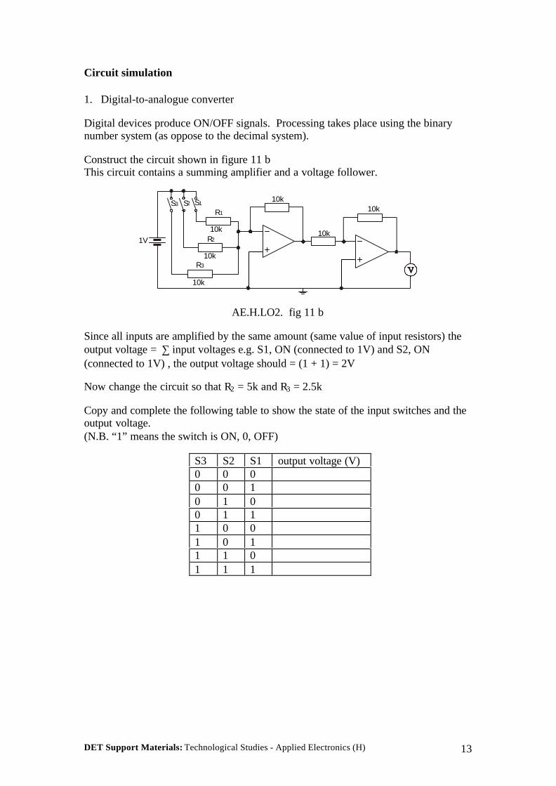
1. Digital-to-analogue converter
Digital devices produce ON/OFF signals. Processing takes place using the binarynumber system (as oppose to the decimal system).
Construct the circuit shown in figure 11 bThis circuit contains a summing amplifier and a voltage follower.
R1
R2
10k
10k
10k
10k10k
10k
R3
S1S2S3
1V
AE.H.LO2. fig 11 b
Since all inputs are amplified by the same amount (same value of input resistors) theoutput voltage = ∑ input voltages e.g. S1, ON (connected to 1V) and S2, ON(connected to 1V) , the output voltage should = (1 + 1) = 2V
Now change the circuit so that R2 = 5k and R3 = 2.5k
Copy and complete the following table to show the state of the input switches and theoutput voltage.(N.B. “1” means the switch is ON, 0, OFF)
S3 S2 S1 output voltage (V)0 0 00 0 10 1 00 1 11 0 01 0 11 1 01 1 1

DET Support Materials: Technological Studies - Applied Electronics (H) 14
2. a.c. mixer pre-amplifier
Mixers allow different signals to be amplified by different amounts before being fedto the main amplifier. Signals might come from microphones, guitar pick-ups, vocals,pre-recorded sound tracks etc.
Construct the circuit shown in figure 11 cAdjust the frequencies of the signals as shown and adjust the oscilloscope to give amaximum voltage of 10 V and a minimum of -10 V.
S2 S3S110k
0.25Hz O.5Hz 0.75Hz
Putting each switch on individually will allow you to “see” each of the input signals inturn.
Putting more than one switch on at a time will show you the sum of the input signals.Adjusting the size of the input variable resistors alters the amplification of thatparticular input signal.
(Complex output signals can be constructed by adding sine waves of the correctamplitude and frequency - useful in electronic keyboards or synthesisers when aparticular musical instrument is required.)
AE.H.LO2. fig 11 c
DET Support Materials: Technological Studies - Applied Electronics (H) 15
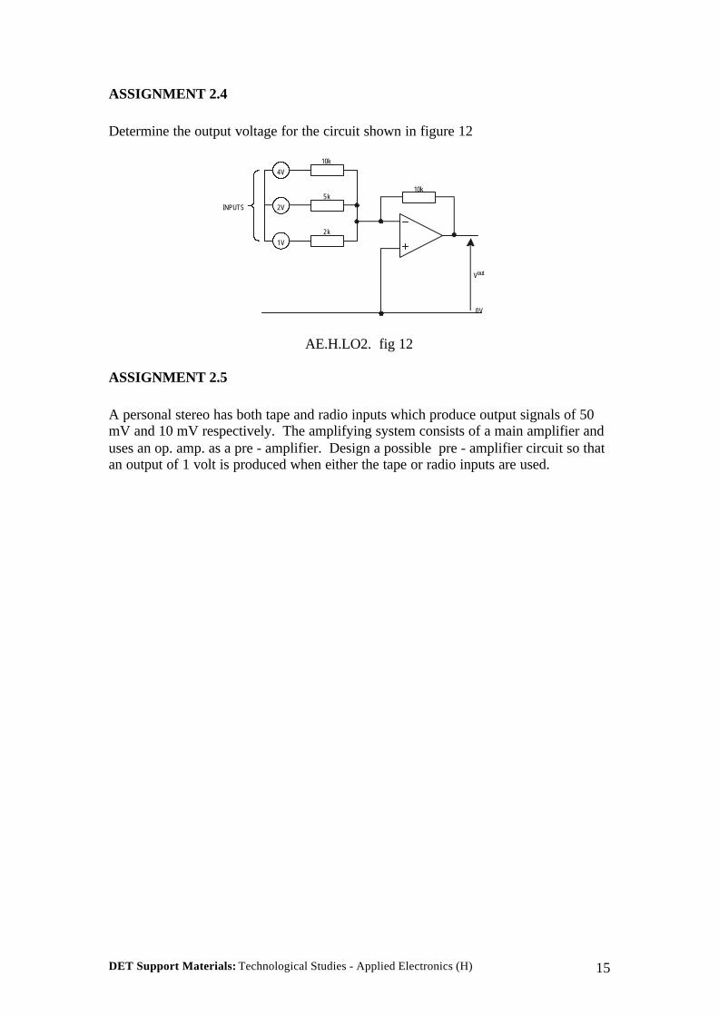
ASSIGNMENT 2.4
Determine the output voltage for the circuit shown in figure 12
Vout
0V
4V
2V
1V
10k
10k
5k
2k
INPUTS
AA
AE.H.LO2. fig 12
ASSIGNMENT 2.5
A personal stereo has both tape and radio inputs which produce output signals of 50mV and 10 mV respectively. The amplifying system consists of a main amplifier anduses an op. amp. as a pre - amplifier. Design a possible pre - amplifier circuit so thatan output of 1 volt is produced when either the tape or radio inputs are used.

DET Support Materials: Technological Studies - Applied Electronics (H) 16
The difference amplifier configuration
Here both inputs are used. The op. amp. amplifies the difference between the twoinput signals.
V1
V2Vout
R1
R2
Rf
R3
0V
AE.H.LO2. fig 13
To ensure that each input is amplified by the same amount, the circuit is designed sothat the ratio:
R
RRR
f
1
3
2
=
To ensure that the input resistance of the circuit for each input is the same,R1 = R2 + R3
Characteristics of the difference amplifier
AR
RVf=1
VR
RV Vout
f= × −1
2 1( )
input resistance = R1
Note:if R1 = Rf then AV = 1 and Vout = (V2 - V1) , the circuit works as a "subtracter".the output will be zero if both inputs are the same.
This circuit is used when comparing the difference between two input signals.

DET Support Materials: Technological Studies - Applied Electronics (H) 17
ASSIGNMENT 2.6
Two strain gauges are connected to a difference amplifier as shown in figure 14
Rg Rg2
Ra
6V
Vout
0VAA
4k2
390R
39k
42kRb
Y
X
AE.H.LO2. fig 14
RA = RB = 1 k, when not under strain, Rg1 = Rg2 = 200 Ω
a) Calculate the voltage at X and Y when both gauges are not under strain and hencedetermine the output voltage of the amplifier.
b) As the strain of Rg2 increases, its resistance increases from 200 to 210 Ω ,determine the new output voltage.
c) What would you expect to happen to the output voltage if both gauges were putunder the same amount of strain?

DET Support Materials: Technological Studies - Applied Electronics (H) 18
The comparator configurationThis is a special case of the difference amplifier in which there is no feedback (see fig15). The gain of the circuit is therefore Ao and any small difference in the two inputsignals is amplified to such an extent that the op. amp. saturates (either positively ornegatively).
V1V2
Vout
AA0V
AE.H.LO2 fig 15
AV = Ao Vout = Ao x (V2 - V1)
hence if V2 > V1, Vout is positive, if V2 < V1, Vout is negative
This is commonly used in control circuits in which loads are merely switched on andoff.
e.g. The circuit shown in figure 16 would give an indication when the temperaturefalls below a preset value (0oC for example).
-t
Vr
V1
V2
0V
LED
6V
AE.H.LO2. fig 16
Vr is adjusted until V1 is just greater than V2, the output will therefore be negative andthe led will be off.As the temperature falls, the resistance of the ntc thermistor rises and therefore V2starts to rise. Eventually, V2 > V1, the output goes positive and the led lights.

DET Support Materials: Technological Studies - Applied Electronics (H) 19
N.B. Since nothing happens when the output of the op. amp. goes negative, thiscircuit could be operated from a single power rail (as oppose to a dual power rail) asshown in figure 17
-t
Vr
V1
V 2
AE.H.LO2. fig 17
Here, when V1 > V2, the output will try and go "as negative as possible" i.e. down to 0volts and the led will be off.

DET Support Materials: Technological Studies - Applied Electronics (H) 20
Driving external loadsThe maximum output current that can be drawn from an op. amp. is usually low(typically 5 mA). If larger currents are required, the output could be connected to atransducer driver either a bipolar transistor or MOSFET (and relay circuit if required).
ASSIGNMENT 2.7Describe the operation of the circuit shown in figure 18 and state the purpose of thevariable resistor Vr and the fixed resistor Rb(for clarity, the d.c. power supply has not been shown)
Vr
Rb
AE.H.LO2. fig 18

DET Support Materials: Technological Studies - Applied Electronics (H) 21
Control systemsIn a control or servomechanism system a feedback loop is included in the circuit. Thismonitors the output and necessary changes are made to ensure that the level of theoutput remains at a constant level.
INPUTSETTING OUTPUT
CONTROL SYSTEM
SENSINGTRANSDUCER
AE.H.LO2. fig 19
The difference between the input setting and the actual output as monitored by thetransducer will produce an error. This error is then used to alter the output of thecontrol system.e.g. The temperature control of a freezer is set at a given value. A transducer thenmonitors the temperature and switches the freezer pump on and off accordingly.
In a non-feedback system (sometimes known as an open-loop system), the inputs areadjusted to give the expected output and then left.Changes in conditions (load, environment, wear & tear etc.) may result in the outputvarying from the level set by the inputs. These changes are not taken into account bythe open-loop system.For example, the speed of an electric motor may be set by an input variable resistor,load on the motor however will cause it to slow down and the output speed will beless than expected for the given input conditions.
In it's simplest form, a feedback (or closed-loop) system provides an on/off output inwhich a mechanical or electronic relay, switches the power circuit on or off. Thison/off operation will cause the output to "hunt" above and below the required level.In some cases, an on/off system may be all that is required.
A better form of feedback loop is where the output is proportional to the differencebetween the preset level and the feedback signal. This results in smoother control, forexample, in an electrical heater where the output power of the heater can be variedaccording to the difference between the preset temperature and the actual temperature.If the temperature difference is large, the heater might be working at full power, as thetemperature of the room increases, the temperature difference between the presetvalue and the actual temperature will decrease and therefore the output power of theheater will decrease.

DET Support Materials: Technological Studies - Applied Electronics (H) 22
PRACTICAL ASSIGNMENT 2.1
Measurement of motor speedsThe speed of a rotating shaft or spindle can be measured by attaching a disc with asection cut out.
A schematic diagram of the circuit is shown below.
PROCESSUNIT
MOTOR
LIGHT SOURCE
LIGHTSENSOR
DISC WITHSLIT
OSCILLOSCOPE
AE.H.LO2. fig 20
A light source and sensor are placed on either side of the disc.As the shaft rotates, the light beam is interrupted. The time taken for one completerevolution can be measured using a calibrated CRO.
TIME FOR
AE.H.LO2. fig 21
Two possible circuits, one using a photo diode and another using an LDR are shownbelow.
+15V
-15V
0V
Vout
1M
+15V
-15V
0V
Vout
100k
LDR 10k
10k
AE.H.LO2. fig 22 fig 23

DET Support Materials: Technological Studies - Applied Electronics (H) 23
Investigate each circuit and suggest with reasons which one should be used.(Start the motor at a low speed and make sure that pulses are obtained on the CROthen slowly increase the speed until the motor is at it's working speed.)
The speed of a lathe can be measured if a white line is painted on the spindle. Whatchanges if any would have to be made to the sensor?

DET Support Materials: Technological Studies - Applied Electronics (H) 24
PRACTICAL ASSIGNMENT 2.2
Air conditioning systemMost domestic central heating systems only operate when the temperature is below apreset level. In an air conditioning system, the temperature of the room air is not onlyheated when the temperature is too low but the air can also be cooled when thetemperature is too high. This could easily be done by incorporating a fan.In the circuit diagram shown below, the motor represents the fan and the bulbrepresents the heater.
1k
-t
47k 10k
22k
0V
AE.H.LO2. fig 24
This particular circuit has at least one drawback. By investigating the circuit, suggestwhat this is and how it could be overcome.(Note: wires are not joined where the lines of the circuit diagram cross over unless thecrossover point is marked by a dot.)

DET Support Materials: Technological Studies - Applied Electronics (H) 25
PRACTICAL ASSIGNMENT 2.3
Measurement of loadStrain gauges can be used to investigate the load on particular members of aconstruction. The resistance of a strain gauge depends on whether it is under tensionor compression. It will also however depend on temperature.
The diagram below shows a single strain gauge bonded to the upper face of a metalstrip.
CLAMP
STRAINGAUGE
METALSTRIP
LOAD
AE.H.LO2. fig 25
As loads are placed on the strip, it bends, stretches the strain gauge which in turnchanges resistance. This change in resistance can be amplified using a differential op.amp. Circuit as shown below.
1M
1M1k
47k
1k 560R
10k
10k
+15V
0V
-15V
RgVout
AE. H.LO2. fig 26

DET Support Materials: Technological Studies - Applied Electronics (H) 26
Construct the circuit as shown, adjust the variable resistor so the voltmeter reads zerowhen no load is applied to the metal strip.
Determine if the voltage output is proportional to the load applied to the strip.
Since the resistance of the gauge also depends on temperature, any temperaturechange will be "recorded" as a change in load. In order to overcome this, it is normalto use two strain gauges in a voltage divider circuit.
1M
1M1k
47k
1k
10k
10k
+15V
0V
-15V
Rg
Rg
Vout
AE. H.LO2. fig 27
Assuming both gauges remain at the same temperature, they will both changeresistance by the same amount and therefore the circuit will remain in balance.
Further, if the second gauge is placed beneath the strip, as load is added, the firstgauge will be under tension while the second will be in compression. This will have adoubling effect.

DET Support Materials: Technological Studies - Applied Electronics (H) 27
END-OF-UNIT ASSIGNMENT
1. An op. amp. is connected as shown in figure Q1.
50k
100k
VoutVin
0V
AE.H.LO2. fig Q1
The input to the circuit is monitored by a single beam oscilloscope, figure Q2 showsthe screen display and the control settings.
y - GAINVolts/cm
TIMEBASEms/cm
1.0 2.0
5.00.5
0.1
1.050
100
500
AE.H.LO2. fig Q2
a) Determine the frequency of the pulses at the input.
b) Assuming the oscilloscope controls are not adjusted, redraw the trace you wouldexpect to see if the oscilloscope was connected to the output of the circuit.
c) The same components are now used to wire the op. amp. in the non-invertingconfiguration. Re-draw the new circuit diagram and the you would expect at theoutput this time.
2. When a tacho generator is rotated, it produces a voltage proportional to it's angularvelocity. The tacho is to be used to monitor the speed of coolant flowing along apipe. If the speed is below a recommended level then an alarm should come on, ifthe speed is above this level then a green light should come on.Draw a circuit diagram of the system that could be used and explain how thesystem works.

DET Support Materials: Technological Studies - Applied Electronics (H) 28
3. Part of a disco audio system consists of the microphone connected to a circuitcontaining two op. amps. as shown in figure Q3
1k
1M
6V
MICROPHONE
AE.H.LO2. fig Q3
a) Explain clearly how the circuit operates.
b) Why are two op. Amps. used in this circuit?
4. A robot is designed to follow a white line painted on the floor. The robot movesby means of suitably geared motors which can be switched on and offindependently.
WHITELINE
AE.H.LO2. fig Q4

DET Support Materials: Technological Studies - Applied Electronics (H) 29
The left sensor controls the right motor (and vice versa). When a sensor detects awhite line, the motor is switched on.
a) Suggest a suitable detector that could be used to detect the white line.
b) Explain how the robot follows the white line.
c) Design a suitable circuit that could be used to control one of the motors.

DET Support Materials: Technological Studies - Applied Electronics (H) 30
SEB & SQA PAST PAPER EXAM QUESTIONS
1993, Paper 1, question 1
(a) Name the configuration of the amplifier shown in figure Q1(b) Calculate the gain of the amplifier.(c) (i) If the input signal Vi is 0.5 V, what is the value of the output signal Vo?
(ii) Explain your answer.
100k
2k
+15V
-15V
0V
V0V1
AE.LO2. fig Q1
1997, Paper 1, question 6
Figure Q2 shows an operational amplifier circuit, which includes an ORP12 lightdependent resistor as an input sensor. When the light level on the LDR is 50 lux, determine:(a) the resistance of the LDR;(b) the voltage gain of the operational amplifier;(c) the current flowing through the load resistor RL, stating clearly the direction in
which it is flowing.
ORP12
1k
6k
A
B
R = 300RL4V
+Vcc
-Vcc
AE.LO2. fig Q2

DET Support Materials: Technological Studies - Applied Electronics (H) 31
1994, Paper 1, question 10
A technological experiment involves recording the total effects of light andtemperature. It utilises an operational amplifier configured as shown in figure Q3A.
t
3k5
10k
20k
20k
10k
+9V
-9V
0V
Vo
AE.LO2. fig Q3A
(a) Name the configuration of the amplifier used in the experiment.(b) Explain clearly how the system operates.(c) Determine the gain of the amplifier.(d) Comment on the suitability of the value of the gain in this particular circuit.
The following graph Figure Q3B shows the actual temperature and light readingsrecorded during the experiment between the hours of 1400 and 2000 on one particularday.The characteristics of the light dependent resistor and the thermistor used in the circuitare shown in figure Q3C.
TEMP(oC)LIGHT(LUX)
TIME OF DAY1400 1500 1600 1700 1800 1900 2000
50
40
30
20
10
1000
800
600
400
200
TEMPERATURE
LIGHT
AE.LO2. fig Q3B

DET Support Materials: Technological Studies - Applied Electronics (H) 32
(e) Determine the output voltage (Vo) from the circuit in figure Q3A at 1700 hours.(f) For later processing, this value of (Vo) must be positive.
(i) Name an additional device which can be added to the circuit to produce apositive value for Vo.
(ii) Draw the circuit symbol for this additional device and indicate the value ofany components used.

DET Support Materials: Technological Studies - Applied Electronics (H) 33
1997, Paper 1, question 9(part)
A deep-fat fryer incorporates a cooking oil temperature indicator. An array of LEDsis shown on the control panel and, as the temperature of the cooking oil increases, theLEDs light in a ladder sequence. (Figure Q4A)
LEDs
AE.LO2. fig Q4A
The circuit shown in figure Q4B is used to control the lighting of the LEDs. Thecircuit utilises three 741 operational amplifier Ics and a 151-164 thermistor.
t
12V
0V
-12V
400R
300R
200R
100R 15k
C
B
A
AE.LO2. fig Q4B

DET Support Materials: Technological Studies - Applied Electronics (H) 34
(a) In which amplifier mode are the 741 Ics being used ?(b) Explain in detail why the LEDs light up in sequence as the temperature of the oil
increases. The function of the components in the circuit should be included inyour explanation.
(c) At what temperature will LED “C” light ?(d) If the current through each LED is to be limited to 200 mA, determine what value
of resistor should be connected in series with each LED. (Ignore any voltage dropacross the LEDs.)
1998, Paper 1, question 7
A camera manufacturer is evaluating a design for a light level indicator, details ofwhich are shown in Figure Q5.
For this circuit, determine the range of values of the input voltage Vin over which theLED will glow to indicate that a photograph may be taken.Show all calculations
+Vcc +Vcc
-Vcc -Vcc
4k
16k
6k
4kVin
+5V
0V
AE.LO2. fig Q5

DET Support Materials: Technological Studies - Applied Electronics (H)
TECHNOLOGICAL STUDIES
HIGHER
APPLIED ELECTRONICS
SECTION 3
OUTCOME 3

DET Support Materials: Technological Studies - Applied Electronics (H)

DET Support Materials: Technological Studies - Applied Electronics (H) 1
APPLIED ELECTRONICS
Outcome 3 - Design and construct combinational logic systems to meet givenspecifications
When you have completed this unit you should be able to:• Identify single logic gate symbols• Complete Truth Tables for single logic gates• Analysis Combinational logic circuits• Complete Truth Tables for combinational logic circuits• Simplify combinational logic circuits• Write a Boolean expression for a given logic circuit• Determine equivalent circuits made from NAND gates• Identify differences between the TTL and CMOS families of IC's• Identify types of logic gates, given pin layout diagrams or IC number (logic gate
IC's)• Correctly 'power up' an IC for uses - either diagrammatically or on breadboard• Using pin diagrams, select correct IC's and be able to form circuits to given
specification
Before you start this unit you should have a basic understanding of:
Input and Output transducers.Voltage divider circuits.Ohm’s Law - relationship between V and I in a d.c. circuit.The operational characteristics of various electronic components.Use of breadboards.Use of circuit test equipment: multimeter and oscilloscope.

DET Support Materials: Technological Studies - Applied Electronics (H) 2
BASIC LOGIC GATES
There are seven different logic gates; these are the NOT, AND, OR, NAND, NOR,XOR and the XNOR.
When drawing circuits containing logic gates it is common to use logic symbols. Twosets of symbols might be used.
American Military Symbols (ANSI) Used in this and other countriesBritish Standard Symbols (BS3939) Used in this country
NOT
AND
NAND
OR
NOR
AMERICAN SYMBOLS
1
&
&
BRITISH SYMBOLS
AE.H.LO3. fig1
Throughout this course the more common American symbols will be used. These arethe symbols used by the SQA. You should however be familiar with both sets.

DET Support Materials: Technological Studies - Applied Electronics (H) 3
Truth TablesThe easiest way to represent how each gate behaves is to make use of Truth Tables.A Truth Table shows all possible combinations of inputs and outputs to a logic gate.Electronics is concerned with the processing of electrical signals.
INPUT PROCESS OUTPUT
AE.H.LO3. fig 2
Input signals come from a variety of sources - a switch from a keyboard; a bar codereader; a temperature sensor; another part of a computer.
Output signals can have a variety of destinations - a monitor; a modem; an alarm;another part of a computer.
Digital signals can be at a HIGH voltage level or a LOW voltage level.In logic circuits a LOW signal is said to be at logic '0' a HIGH signal at logic ' 1'.The results can be recorded and used in a number of formats, the most common beingshown below.
LOGICGATE
PROCESS
A
B
INPUTS OUTPUTSINPUTS OUTPUTS
A B0011
0101
0110
AE.H.LO3. fig 3
Results displayed in this way are known as TRUTH TABLES.
Structure and layout of Truth TablesConsider the inputs to a logic gate as two switches.
INPUT B
INPUT AOUTPUT
+Vcc
AE.H.LO3. fig 4
It is possible for each switch to be in one of two positions, either, on (1) or off (0).These positions are known as INPUT STATES.

DET Support Materials: Technological Studies - Applied Electronics (H) 4
For two inputs, there are only 4 possible combinations of input states:
A-off & B-off; A-off & B-on; A-on & B-off; A-on & B-on.
Input A Input B0 00 11 01 1
For three inputs, there are 8 possible combinations.
In general, for n inputs there are 2n possible combinations of input states(and hence 2n lines in the truth table.)
ASSIGNMENT 1
1. How many combinations of input states would there be for a 6 input system ?
2. Write down the 8 possible combinations of input states for a 3 input system.

DET Support Materials: Technological Studies - Applied Electronics (H) 5
Truth Tables for Individual logic gates
Circuit Simulation SoftwareIt is possible to use circuit simulation software such as ‘Crocodile Clips’ to investigateelectric and electronic circuits.Collect a copy of the worksheet “Truth tables”.Use ‘Crocodile Clips’ or another similar software package to determine the truth tablefor each of the following gatesUse switches at the inputs and an indicator at the output.(N.B. When the switch or indicator is off, the signal is at logic 0.)
1. NOT gate
AE.H.LO3. fig 5
2. AND gate
AE.H.LO3. fig 6
3. OR gate
AE.H.LO3. fig 7

DET Support Materials: Technological Studies - Applied Electronics (H) 6
4. NAND gate
AE.H.LO3. fig 8
5. NOR gate
AE.H.LO3. fig 9
6. XOR gate
AE.H.LO3. fig 10
ASSIGNMENT 2
1. When is the output of an OR gate high ?
2. When is the output of an AND gate high ?
3. When is the output from an XOR gate high ?(‘X’ stands for exclusive)
4. Why is the NOT gate sometimes called an ‘INVERTER’ ?

DET Support Materials: Technological Studies - Applied Electronics (H) 7
5. The truth table below shows the output conditions for the various combinations ofinput conditions for AND, NAND, OR and NOR gates.
Inputs AND NAND OR NOR0 0 0 1 0 10 1 0 1 1 01 0 0 1 1 01 1 1 0 1 0
How does the output of the NAND gate compare with the output of the AND (and theoutput of the NOR compare with the OR)
6. The paper can be fed through a computer printer either by pressing the button onthe printer (line feed) or by sending a signal from the computer.
COMPUTERSIGNAL
PRINTERBUTTON
PAPERFEED
AE.H.LO3. fig 11
Which logic gate should be used for this operation ?
7. The motor in a washing machine should not operate until a high signal is sentfrom the control program and the water level in the drum is high enough.
WATERLEVELSENSOR
CONTROLPROGRAM
MOTOR
AE.H.LO3. fig 12
Which logic gate should be used for this operation ?

DET Support Materials: Technological Studies - Applied Electronics (H) 8
8. To avoid accidents at times of poor visibility, a warning indicator in a car operatesif the light level is too low (logic level 0) and the headlamps are switched off.
LIGHTLEVELSENSOR
HEADLAMPSSWITCH
WARNINGINDICATOR
AE.H.LO3. fig 13
Which logic gate should be used for this operation ?
9. In the maternity unit of a hospital, the temperature and pulse rate of prematurebabies has to be continually monitored. A warning alarm should sound if eitherthe temperature or the pulse rate of the baby falls too LOW.
TEMPERATURESENSOR
PULSERATESENSOR
WARNINGALARM
AE.H.LO3. fig 14
Which logic gate should be used for this operation ?

DET Support Materials: Technological Studies - Applied Electronics (H) 9
Gate NetworksIt is often necessary to use more than one gate to perform a decision process.For example, on some TV sets it is possible to change the channel either by pressingthe channel select button on the TV or by pressing the channel select button on theremote control. The channel will only change however, if the TV set is switched on.i.e. The channel will change if the TV set button is pressed OR the remote button ispressed AND the TV set is on.
A logic diagram for this is shown in figure 15
REMOTEBUTTON
TV SETBUTTON
TV ON/OFFSWITCH
CHANNELSELECT
AE.H.LO3. fig 15
Analysing a combinational logic systemCOMBINATIONAL LOGIC circuits are those in which the output at any time isdetermined entirely by the combination of input signals which is present at that time.i.e. the output state does not depend on the sequence of the input signals.
In digital electronics we often encounter systems which will contain several logicgates that have been combined together.Suppose that you need to know how a particular network will behave for eachpossible combination of inputs.
If a logic diagram is given, for example:
AE.H.LO3. fig 16

DET Support Materials: Technological Studies - Applied Electronics (H) 10
STEP 1Label all the different points on the circuit, including inputs and outputs.Notice that one input serves two gates, this is quite common in logic circuits and bothgates should be labelled accordingly.
AB
C
BD (OUTPUT)
AE.H.LO3. fig 17
STEP 2Draw up a Truth Table for the circuit, with a different column for each letter.NB. determine the number of input conditions for the truth table.
two input, therefore 22 = 4
i.e. 4 lines on the truth table.
INPUTA B C
OUTPUT D
0 00 11 01 1
STEP 3Determine what goes into column C. To do this, consider the OR gate on its own,with inputs A and B, enter findings into column C.
AB
C
AE.H.LO3. fig 18
INPUTA B C
OUTPUT D
0 0 00 1 11 0 11 1 1

DET Support Materials: Technological Studies - Applied Electronics (H) 11
STEP 4Determine what goes into column D i.e.. the output column. Consider the AND gateon its own with inputs from C and B enter findings into column D.
C
BD (OUTPUT)
AE.H.LO3. fig 19
INPUTA B C
OUTPUT D
0 0 0 1 1 1 0 1 0 1 1 1
STEP 5Your final answer should look like this
INPUTA B
OUTPUT
0 0 00 1 11 0 01 1 1
A more complicated system may need several stages before you finish, but if youwork systematically through the circuit in the way shown, considering one gate at atime, you should arrive at the correct answer.

DET Support Materials: Technological Studies - Applied Electronics (H) 12
ASSIGNMENT 3
Complete a truth table for each of the combinations of gates shown below.
1.
AE.H.LO3. fig 20
2.
AE.H.LO3. fig 21
3.
AE.H.LO3. fig 22
4.
AE.H.LO3. fig 23

DET Support Materials: Technological Studies - Applied Electronics (H) 13
5.
AE.H.LO3. fig 24
Any of the above circuits can be constructed and tested using circuit simulationsoftware such as ‘Crocodile Clips’.

DET Support Materials: Technological Studies - Applied Electronics (H) 14
NAND EQUIVALENT CIRCUITS
It is possible to make other logic gates (and circuits) by combining NAND gates.
In practice, it is much easier and cheaper to make NAND gates than any others,indeed NAND gates were the first types of gate to be developed into IntegratedCircuits (IC's).Frequently, a circuit will be made entirely from NAND gates. Although it is possibleto use NOR gates as the basic logic unit, the industry standard is the NAND gate.The use of only one type of gate to make a circuit often allows us to simplify thewiring of a system and makes more efficient use of an Integrated Circuit.Most NAND logic gate IC's contain a number of gates - usually four - and cost aslittle as a few pence for each IC.The figure below shows a pin layout diagram of a NAND logic gate IC. This IC has 4independent 2 input NAND gates
21 3 4 5 6 7
14 13 12 11 10 9 8
+Vcc
Gnd(0V)
AE.H.LO3. fig 25
The section on IC's will explain in greater detail about the layout and nature of IC's.

DET Support Materials: Technological Studies - Applied Electronics (H) 15
METHODS OF MAKING SPECIFIC GATES FROM NANDS
Circuit Simulation SoftwareIt is possible to use circuit simulation software such as ‘Crocodile Clips’ to investigateelectric and electronic circuits.Collect a copy of the worksheet “NAND equivalent circuits” .Use ‘Crocodile Clips’ or another similar software package to determine the truth tablefor each of the following network of NAND gates.Compare the truth table you obtain with truth tables for the individual gates anddecide which gate is the equivalent to the NAND network.(N.B. In some of the networks the two inputs of the NAND gate have been connectedtogether to make a single input.)
1.
AE.H.LO3. fig 26
2.
AE.H.LO3. fig 27
3.
AE.H.LO3. fig 28
4.
AE.H.LO3. fig 29

DET Support Materials: Technological Studies - Applied Electronics (H) 16
Simplification of Combinational Logic CircuitsAs has previously been stated it is possible to make all logic circuits from NANDgates only.This section will examine a method for converting circuits that contain a number ofdifferent types of gates into one that uses NAND gates only.
Consider the circuit shown.
A
B
B
D
CZ
AE.H.LO3. fig 30
The system is made from an AND gate an OR gate and a NOT gate.The problem is to design a system with the same Truth Table, but made from NANDgates only.
STEP 1Redraw the circuit, replacing each gate with its NAND gate equivalent.
1 2
3
4
5
6
A
B
C
D
Z
AND
OR
NOT
AE.H.LO3. fig 31

DET Support Materials: Technological Studies - Applied Electronics (H) 17
STEP 2Examine the new arrangement and look for adjacent pairs of NOT gates.In this circuit there are two such pairs. (2 & 3 and 4 & 5 are adjacent pairs)If you consider what happens when you feed a signal to a NOT gate then pass thesignal on to another NOT gate you will find that the signal has been 'DOUBLEINVERTED' this in fact means that whenever you feed a signal to a pair of NOTgates you will get the same signal out.
A
B
Z
AE.H.LO3. fig 32
Therefore pairs of NOT gates in series can be removed from the system without anyeffect. (This fact is of considerable importance when we come on to the next sectionon Boolean algebra.)
STEP 3Redraw the circuit with the NOT gates removed.
A
B
Z
AE.H.LO3. fig 33
The final circuit has only two gates whereas the original circuit started with threegates, each of a different type. There are obvious implications in terms of cost formanufacturers if they are able to reduce logic circuits to situations where there arefewer gates as well as enabling them to use one type of gate. The original circuitwould have required three IC's and the final circuit would only require one IC.
This method may not reduce the number of gates used on every occasion but it shouldreduce the number of IC's used.
This method is not very elegant and can be very demanding in terms of paper use anddoes not always lead to a very efficient use of NAND gates. The next section onBoolean algebra should allow us to design circuits more effectively and use fewergates.

DET Support Materials: Technological Studies - Applied Electronics (H) 18
ASSIGNMENT 4The following logic diagrams are constructed from basic gates. Using the methodshown, construct equivalent circuits using NAND gates only.
1.
AE.H.LO3. fig 34
2.
AE.H.LO3. fig 35
3.
AE.H.LO3. fig 35a
4. a) Construct a truth table for the logic circuit shown.
A
B
C
b) Redraw the circuit using NAND gates only.c) Simplify the NAND circuit.d) Construct a truth table for the finished NAND circuit.

DET Support Materials: Technological Studies - Applied Electronics (H) 19
Boolean AlgebraBoolean algebra is a special form of algebra that has been developed for binarysystems. It was developed by George Boolean in 1854 and can be very useful forsimplifying and designing logic circuits.
Variables:The most commonly used variables in logic circuit design are capital letters; such asA, B, C, Z and so on and are used to annotate inputs and outputs to systems.In digital electronics we consider situations where the variables can only have one oftwo possible values, i.e. 'Logical 0' or 'Logical 1'.
The statement A = 1 means that the variable A has the value of Logic 1. Similarly, ifB = 0 it means that variable B has the value of logic 0.
Logical Operations: In Boolean algebra there are three logical operators, these are theAND operation, the OR operation and the Inversion.
AND OperatorThe AND operation can be represented in Boolean notation by
A • B = Z
The dot between the A and the B is read as AND.
OR OperatorThe OR operation can be represented in Boolean notation by
A+B = Z
The + between the A and the B is read as OR.
Inversion OperatorThe statement A = Z means that Z is not equal to A.The variable is read as A bar and usually means NOT A . The bar over the top of thevariable changes it's value, or inverts it. This is known as the NOT operation.

DET Support Materials: Technological Studies - Applied Electronics (H) 20
Basic logic gates and their Boolean representations
NOT
AND
OR
LOGIC SYMBOL BOOLEANEXPRESSION
A.B = Z
A+B = Z
DESCRIPTION
A = Z NOT EQUALS A Z
A B Z AND EQUALS
A B Z OR EQUALS
TRUTH TABLE
A01
Z10
A0011
B0101
Z0001
A0011
B0101
Z0111
AE.H.LO3. fig 36

DET Support Materials: Technological Studies - Applied Electronics (H) 21
NAND gateThe NAND gate is made up from a combination of an AND gate followed by a NOTgate.
AB
ZC
AE.H.LO3. fig 37
The signal at point C would be A• B. This signal is then inverted by the NOT gate togive
A B Z• =
This reads as output Z is equal to A AND B all NOT

DET Support Materials: Technological Studies - Applied Electronics (H) 22
NOR gateThe NOR gate is made up from a combination of an OR gate followed by a NOT.
AB
ZC
AE.H.LO3. fig 38
The signal at point C would be A+B. This signal is then inverted by the NOT gate togive
A B Z+ =
This reads as output Z is equal to A OR B all NOT

DET Support Materials: Technological Studies - Applied Electronics (H) 23
ASSIGNMENT 5Write down the Boolean expression for each of the following logic gates.
A
BZ
a)
A
BZ
d)
AB ZC
g)
A
BZ
b)
A Z
e)
AB
ZCD
h)
A
BZ
c)
AB ZC
f)
AB
ZCD
i)
AE.H.LO3. fig 39
Laws of Boolean AlgebraThe following is a summary of the basic laws of Boolean algebra. These are the mostcommonly used laws . Your teacher will assist you if you require further information.
NB. It is essential to understand whilst undertaking analysis using Boolean that youmust not confuse the symbols used for the Logical operators with those used innormal algebra.
It is perhaps useful to know that the rules of common algebra are the same as those ofBoolean.
+ represents logical operator OR• represents Logical operator ANDA represents A bar i.e. NOT A ( the inverse of A)

DET Support Materials: Technological Studies - Applied Electronics (H) 24
Deriving the Boolean expression for a circuit
Consider the following circuit.
AE.H.LO3. fig 39a
The Boolean expression for the circuit can be derived as follows:
STEP 1Label the inputs on the left-hand side of the diagram.(If one input serves more than one gate ensure that the input is labelled accordingly).
A
B
B
AE.H.LO3. fig 40
STEP 2Consider each gate in turn. Use the Boolean notation (operators) to give the output ofeach gate in terms of its input.Write on the appropriate expression after each gate.
A
B
B
A.B
B
AE.LO3. fig 40a

DET Support Materials: Technological Studies - Applied Electronics (H) 25
STEP 3When outputs from other gates are inputs to a further gate, treat the expressions asyou would any other equation and make use of brackets (if necessary). Then write onthe appropriate expression after the next gate and so on until you reach the finaloutput.
A.B
B(A.B) + B
AE.H.LO3. fig 41
STEP 4Write down the final Boolean expression for the network.
( )A B B Z• + =
(Since normal rules of algebra hold, B A B Z+ • =( ) would also be correct)

DET Support Materials: Technological Studies - Applied Electronics (H) 26
ASSIGNMENT 6 a1. Derive the Boolean expression for each of the following circuits:a) b)
c) d)
A
B
C
D
e) f)
A
B
C
A
B
2. Draw a gating arrangement to illustrate Z A B C= • +
3. Draw a logic diagram to yield D B C= +Develop it to obtain Z A D= •Write a Boolean equation for the overall behaviour.
4. Derive the Boolean equation and the truth table the following arrangements:
a) b)
A
B
C
A
B
C

DET Support Materials: Technological Studies - Applied Electronics (H) 27
5. For each pair of circuits shown below:
(i) Write a Boolean expression for each of these circuits;(ii) By constructing a truth table for each of them, show that they are eqivalent;(iii) Draw the eqivalent arrangements using only 2-input NAND gates.
a)
A
B
A
B
b)
A
BA
B
c)
A
B
C
A
B
C
AE.H.LO3. fig 42

DET Support Materials: Technological Studies - Applied Electronics (H) 28
Deriving the Boolean expression from a Truth Table
Consider the Truth Table given
A B Z0 0 10 1 01 0 11 1 1
STEP 1Note each combination that will give you a '1' at the output and write the Booleanexpression for this line at the side of the Truth Table, next to the line that it applies to.
A B Z0 0 1 A B•0 1 01 0 1 A B•1 1 1 A B•
STEP 2Join the equations by putting an OR sign between each to give the final Booleanexpression.
( ) ( )A B A B A B Z• + • + • =
ASSIGNMENT 6 b
2. Write the Boolean equation for the following truth tables
a)A B Z0 0 00 1 11 0 11 1 0
b)A B C Z0 0 0 00 0 1 00 1 0 10 1 1 11 0 0 01 0 1 11 1 0 01 1 1 1

DET Support Materials: Technological Studies - Applied Electronics (H) 29
2. Develop a Boolean equation and draw a logic circuit diagram containing AND,OR and NOT gates to yield the truth table shown.
A B C Z0 0 0 00 0 1 10 1 0 10 1 1 01 0 0 11 0 1 01 1 0 01 1 1 0

DET Support Materials: Technological Studies - Applied Electronics (H) 30
Designing a circuit from its Boolean equationConsider the following equation
A B A B A B Z• + • + • =
STEP 1Draw inputs A and B (and any other input variables) on the left-hand side of the page.
A
B
STEP 2Start by considering the first term
A B•
It can been seen from the equation that both inputs require to be inverted. This isachieved by passing signals from A and B through NOT gates. The output from thesesignals are then used as inputs to an AND gate (as signified by the dot between the Aand B in the Boolean expression).
A
BB
A
A.B
AE.H.LO3. fig 43
Write this on the output line of the AND gate.

DET Support Materials: Technological Studies - Applied Electronics (H) 31
STEP 3Consider the next term
A B•
It can be seen from this term that input A does not require to be inverted but input Bdoes. Since we already have both input A and B bar available we can amend thecircuit diagram accordingly by feeding these inputs to a second AND gate.
A
A
BB
A
A.B
A.B
AE.LO3. fig 44STEP 4Consider the final term
A B•
Again both inputs are available to us. Neither of the inputs is inverted so the signalsare taken from the original inputs and are fed to a third AND gate.
A
A
BB
A
A.B
A.B
A.B
AE.H.LO3. fig 45

DET Support Materials: Technological Studies - Applied Electronics (H) 32
STEP 5Finally we use the outputs from the three AND gates as inputs to a three input ORgate to arrive at the final solution.
A
A
BB
A
A.B
A.B
A.B
A.B A.B A.B+ +
AE.H.LO3. fig 46

DET Support Materials: Technological Studies - Applied Electronics (H) 33
ASSIGNMENT 72. For the following Boolean equations, draw the correct logic circuit arrangement.
a) A A B Z+ • =b) A B C Z+ + =c) A B A C Z• + • =d) A B A C B C Z• + • + • =e) A B C D E F G• • + • + •
Combinational logic circuit designAs problems become more and more difficult it is not always possible to go from thequestion to the answer in one or two steps, when that is the case the following set ofrules should be followed.
When designing a system to suit a need you should proceed in the following order.
1. Describe the problem clearly in words.
2. Write out a Truth Table for the system.
3. Derive the Boolean expression from the Truth Table.
4. Simplify this expression if possible.
5. Draw a logic circuit diagram for the system using AND, OR and NOT gates.
6. Convert the circuit to NAND gates only.
It is entirely possible that not every problem will require all of these steps to befollowed, however this will be a useful guide for most.

DET Support Materials: Technological Studies - Applied Electronics (H) 34
WORKED EXAMPLE:The temperature in a manufacturing process is critical.A sensor is used to detect overheating. The sensor normally records a 0 logic level,but when it overheats it records a logic level 1.The signals are detected on a control panel. On the control panel, under normalconditions, a green light is on. If the temperature gets too high the green light goesoff and a red light comes on and a warning bell sounds.The engineer has a switch to cut out the bell, but leaving the red light on. The switchis used when the engineer has noticed the fault on the panel.
This system has two inputs (4 possible combinations) and three outputs (green light,red light and bell).
1. Describe the problem clearly in words.
Let the temperature sensor be input A and the fault acknowledge switch as input B.
Green light is on if: A is 0 AND B is 0OR A is 0 AND B is 1
The second condition occurs if the engineer acknowledges a fault when there is nofault.
The bell rings when: A is 1 AND B is 0
The red light is on when: A is 1 AND B is 0OR A is 1 AND B is 1
2. Write out a Truth Table for the system.
InputsA B
greenlight
redlight
alarmbell
0 0 1 0 00 1 1 0 01 0 0 1 11 1 0 1 0
3. Derive the Boolean expression from the Truth Table.
InputsA B
greenlight
redlight
alarmbell
0 0 1 A B• 0 0
0 1 1 A B• 0 01 0 0 1 A B• 1 A B•1 1 0 1 A B• 0

DET Support Materials: Technological Studies - Applied Electronics (H) 35
4. Simplify the expressions if possible.
green light - ( )A B• +( )A B Z• =It can be seen that the output does not depend on the state of B since the output isHIGH when B is either HIGH or NOT HIGH i.e. the state of the green light dependsonly on the state of A, hence the expression can be simplified togreen light - A Z=
red light - ( ) ( )A B A B Z• + • =Similarly it can be seen that the red light is ON irrespective of the state of B - theoutput only depends on the state of A hence this can be simplified tored light - A Z=
alarm - A B Z• = (can’t be simplified further)
5. Draw a logic circuit diagram for the system using AND, OR and NOT gates.Start with the expression that has fewest terms/gates (in this case A=Z, no gates!)
B
A
RED LIGHT
GREEN LIGHT
ALARM
A
B
A
A.B
AE.H.LO3. fig 47
6. Convert the circuit to NAND gates only.(Look for double inverted signals which can be cancelled out.)
RED
GREEN
ALARM
A
B
AE.H.LO3. fig 48

DET Support Materials: Technological Studies - Applied Electronics (H) 36
ASSIGNMENT 8
1. An electric guillotine must be adequately guarded. In order to safeguard theoperator the machine has two switches, A and B, set about one metre apart, bothof which need to be pressed before the machine will operate.Design a logic circuit that will give a green light if, both switches are not pressedand both switches are pressed. If only one switch is pressed a red light shouldcome on.Assume that the switches return a 0 when not pressed and a 1 when pressed.
2. A given logic circuit has two logic inputs A and B. It is required to produce twologic outputs X and Y according to the following rules:
1. X is to be at logic 1 if (A OR B) but NOT (A AND B) are at logic 1.2. Y is to be at logic 1 if (A AND B) but NOT (A OR B) are at logic 1.
Use the previous method to design an appropriate logic circuit.
3. A garage door is operated by a motor which is controlled by three switches.The motor runs either:when a pressure pad switch, A, in the drive is closed and a light dependentresistor switching circuit, B, is simultaneously activated by the car’s headlightsorwhen the keyswitch, C, in the garage door is operated.
a) Prepare a truth table for all possible combinations of switching conditions forswitched A, B and C. Take switch open as logic 0.
b) From the truth table, prepare a logic diagram using the least number of gates.c) Redesign your circuit to use only 2-input NAND gates.
4. A domestic burglar alarm system is designed such that a bell will operate whenthe power switch is closed and a pressure switch under a carpet is closed or aswitch is opened as a window is lifted.
a) Assuming all switches to be logic state zero (0) when openi) Draw a logic diagram for the design, allocating capital letters to the inputs
to each gate and to the output to the bell.ii) Prepare a truth table for the design. Your table must be headed by the
appropriate letters
b) Show by use of a logic diagrams how you would\modify or combine 3-inputNAND gates to provide AND and OR gates.

DET Support Materials: Technological Studies - Applied Electronics (H) 37
5. The diagram below shows part of an industrial control system having three inputsA, B and C with an output G.
G
FD
E
A
B
C
a) How many different input conditions are possible in this system ?b) What is the function of gates 1 and 2 ?c) Complete a truth table including columns which show the states of D, E, F
and G.d) Why is the design made up entirely of NAND gates ?e) Give an alternative design using 3-input AND and OR gates.
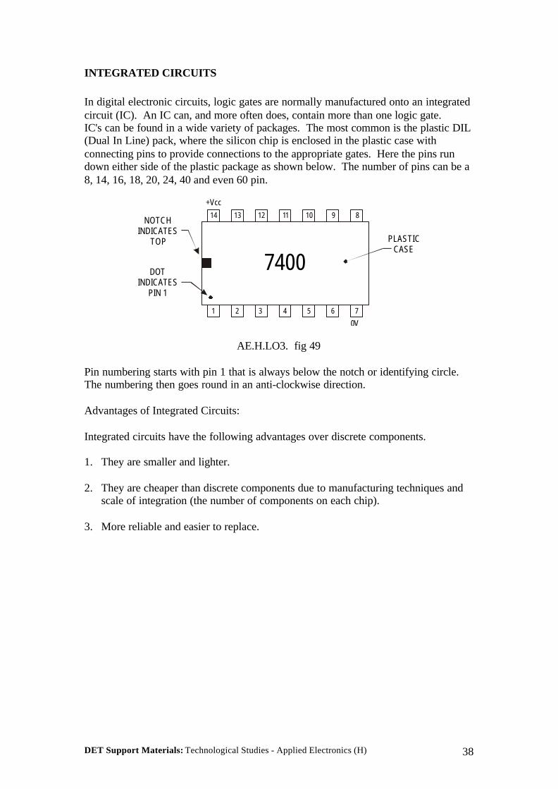
DET Support Materials: Technological Studies - Applied Electronics (H) 38
INTEGRATED CIRCUITS
In digital electronic circuits, logic gates are normally manufactured onto an integratedcircuit (IC). An IC can, and more often does, contain more than one logic gate.IC's can be found in a wide variety of packages. The most common is the plastic DIL(Dual In Line) pack, where the silicon chip is enclosed in the plastic case withconnecting pins to provide connections to the appropriate gates. Here the pins rundown either side of the plastic package as shown below. The number of pins can be a8, 14, 16, 18, 20, 24, 40 and even 60 pin.
21 3 4 5 6 7
14 13 12 11 10 9 8
+Vcc
0V
7400
NOTCH INDICATES
TOP
DOTINDICATES
PIN 1
PLASTICCASE
AE.H.LO3. fig 49
Pin numbering starts with pin 1 that is always below the notch or identifying circle.The numbering then goes round in an anti-clockwise direction.
Advantages of Integrated Circuits:
Integrated circuits have the following advantages over discrete components.
1. They are smaller and lighter.
2. They are cheaper than discrete components due to manufacturing techniques andscale of integration (the number of components on each chip).
3. More reliable and easier to replace.

DET Support Materials: Technological Studies - Applied Electronics (H) 39
Types of Integrated Circuits available (Logic Families):There are two main methods of producing electronic logic devices today, giving twofamilies of logic and these are MOS and TTL.
MOS Logic Devices
MOS stands for Metal Oxide Silicon. MOS devices use field effect transistors(FET's) to make up the gates. Various types of MOS are in use:
CMOS - Complimentary Metal Oxide Silicon referring to the fact that complimentaryp-type silicon and n-type silicon channels are used.
PMOS - Where the channel is made from p-type silicon.
NMOS - Where the channel is made from n-type silicon.
TTL Logic Devices
TTL stand for Transistor - Transistor Logic. These devices use bipolar transistors tomake up the gates
Most switching gate circuits use either Transistor - Transistor Logic (TTL) orComplimentary Metal Oxide Silicon (CMOS) gates.TTL gates are available commercially in the 7400 series and CMOS IC's are availablein the 4000 series.
Comparison of CMOS and TTL devices.The table compares the two types of logic IC's.
Property CMOS TTLSupply voltage
Current requiredSwitching speed
Fan out
3 - 15 V (18Vmax)8 µ Aslow50
5 V ± 0.25V3 mAfast10
NB. A new hybrid chip is available on the market that has the advantages of bothtypes and is listed as the 74HCT00 series. The 74HCT series is a high speed CMOSsemiconductor and has all the advantages of high speed CMOS but with inputsconfigured for direct drop-in replacement of TTL. It operates in the voltage range 2-6V dc.

DET Support Materials: Technological Studies - Applied Electronics (H) 40
CMOS - Advantages1. The main advantage of CMOS devices is that they will operate on any d.c. voltage
in the range 3V-15V (18V max).2. They have a low current drain, usually in the order of a few microamps.3. They have low power consumption.4. They have a high FAN OUT, usually in the order of 50 (the ability of the output of
a gate to drive a number of similar inputs to other gates).5. CMOS has very good noise immunity.
CMOS - Disadvantages1. The major disadvantage of CMOS is it's slower switching speed, usually in the
order of 2 to 4 MHz. (4 x 10⁶ switches per second)2. CMOS devices can easily be destroyed by static electricity (in order to protect
them from static, when in use, all unused inputs should be connected to either thezero volt line or the positive line).
Recent developments in MOS technology have seen major improvements in the areasof speed, with the latest MOS devices claiming speeds similar to TTL.
TTL - Advantages1. The major advantage of TTL devices is their high switching speeds, usually in the
order of 50 MHz (50 x 106 switches per second)2 No damage is done to TTL devices if inputs are left unconnected. (Such inputs
will set to +5V )
TTL - Disadvantages1. TTL devices are much less flexible in terms of their operating conditions than
corresponding CMOS devices.2. Requires a stabilised voltage supply in the range +5V + or - 0.25V (usually
expensive).3. The fan out is 10.4. Higher power consumption than CMOS devices.5. High current drain, usually in the order of a few milliamps.
The latest designs of TTL devices are combining higher and higher switching speedswith lower power dissipation.
In this course we will be using TTL logic gates for demonstrations and practical work,since they are more robust and we can leave the unused inputs floating.

DET Support Materials: Technological Studies - Applied Electronics (H) 41
Identifying Integrated CircuitsThe pin diagram for a 7408 TTL logic gate is shown below.
21 3 4 5 6 7
14 13 12 11 10 9 8
+Vcc
Gnd(0V)
AE.H.LO3. fig 50
The 7408 IC is described as a quad two-input AND gate device.
The quad part indicates how many gates of the type are on the device and the two-input part refers to the fact that each AND gate has two inputs.
Other examples of TTL devices can be found in suppliers' catalogues such as RSComponents.

DET Support Materials: Technological Studies - Applied Electronics (H) 42
EXAMPLES OF PIN LAYOUT DIAGRAMS.
21 3 4 5 6 7
14 13 12 11 10 9 8
+Vcc
Gnd(0V)
21 3 4 5 6 7
14 13 12 11 10 9 8
+Vcc
Gnd(0V)
21 3 4 5 6 7
14 13 12 11 10 9 8
+Vcc
Gnd(0V)
21 3 4 5 6 7
14 13 12 11 10 9 8
+Vcc
Gnd(0V)
21 3 4 5 6 7
14 13 12 11 10 9 8
+Vcc
Gnd(0V)
7404 7400
7421 7420
21 3 4 5 6 7
14 13 12 11 10 9 8
+Vcc
Gnd(0V)7427 7432
AE.H.LO3 fig 51

DET Support Materials: Technological Studies - Applied Electronics (H) 43
ASSIGNMENT 9a) Which of the above IC's contain AND gates.b) Which IC contains 4 input NAND gates.c) Which IC contains NOT gates.d) What type of gate is contained in the 7400 IC.e) Which IC's would be required to construct the following circuits.
a)
b)
c)
AE.H.LO3. fig 52

DET Support Materials: Technological Studies - Applied Electronics (H) 44
IC circuit diagramsThe following logic circuit could be constructed using IC's
INPUT AINPUT B OUTPUT
AE.H.LO3. fig 53
Since the gates within an IC are identical, any one of them can be used
21 3 4 5 6 7
14 13 12 11 10 9 8
21 3 4 5 6 7
14 13 12 11 10 9 8
INPUT A
INPUT B
OUTPUT
AE.H.LO3. fig 54

DET Support Materials: Technological Studies - Applied Electronics (H) 45
ASSIGNMENT 101. The following circuit contains a 7404 and a 7400 IC.
By referring to pin diagrams, draw the corresponding logic circuit.
21 3 4 5 6 7
14 13 12 11 10 9 8
740021 3 4 5 6 7
14 13 12 11 10 9 8
7404
A
B OUTPUT
AE.H.LO3. fig 55
2. Draw the corresponding logic diagram for the circuit shown below.
21 3 4 5 6 7
14 13 12 11 10 9 8
7432
21 3 4 5 6 7
14 13 12 11 10 9 8
7400
21 3 4 5 6 7
14 13 12 11 10 9 8
7404
AB
OUTPUTC
AE.H.LO3. fig 56

DET Support Materials: Technological Studies - Applied Electronics (H) 46
Practical IC circuitsThe following section deals with the construction of circuits containing IC's. You willneed the following equipment.
1. Breadboard.2. 0.7mm solid core insulated wire.3. Various IC's (TTL)only.4. One red led.5. One 330 R resistor.6. 5V regulated supply.7. Three push switches.8. A logic probe.
Pin layout diagram
21 3 4 5 6 7
14 13 12 11 10 9 8
+Vcc
Gnd(0V)
AE.H.LO3. fig 57
The pin layout diagram of a TTL IC is shown above, as previously mentioned, theorientation of the IC is determined from the location of the notch, which indicates thetop and the dot that indicates pin 1.In TTL logic gates, pin 7 is always the ground pin and pin 14 is always the +ve pin,i.e. pin 7 should always be connected directly to 0V or ground and pin 14 shouldalways be connected directly to +5V.

DET Support Materials: Technological Studies - Applied Electronics (H) 47
ASSIGNMENT 11
1. Construct the following circuit using a 7402 IC, two push switches as inputs andan led to indicate the state of the output.
1 7
14 8
7402
SWITCH A
TO +5V
SWITCH B
TO +5V
0V
+5V
TO GND
330R
AE.H.LO3. fig 58
Construct a Truth table for this circuit and determine the single gate that could replacethis NOR equivalent circuit.
2. Construct the following circuit using a 7400 IC, two push switches as inputs and alogic probe on pin 8 to indicate the state of the output. (Power supply and switchconnections have been omitted for clarity.)
21 3 4 5 6 7
14 13 12 11 10 9 8
7400
OUT
A B
AE.H.LO3. fig 59

DET Support Materials: Technological Studies - Applied Electronics (H) 48
Construct a Truth table for this circuit and determine the single gate that could replacethis NAND equivalent circuit.
3. The guard on a machine must be in place before the machine will operate. A pushswitch is ON when the guard is in place. If the machine is switched ON when theguard is not in place, it will not operate and an alarm will sound.
Truth tableInputs
guard machineOutputs
alarm machine0 0 0 00 1 1 01 0 0 01 1 0 1
a) Write Boolean expressions for the two HIGH output states.
b) Draw a logic diagram for the circuit.
c) Use a circuit simulation package (e.g. ‘Croc clips’) to check that your circuit iscorrect.
d) Draw a wiring diagram for the circuit using a 7404 and a 7408 IC.
e) Construct the circuit using a red led for the alarm and a green led to show that themachine is operating.
4. A latch circuit is used when we wish the output signal to remain HIGH even whenthe actuating input signal returns to its original value, e.g. when a burglar alarm isset off, it should keep going until it is reset (either manually or by a timer) even ifthe burglar is no longer there.A simple latch can be made using a single OR gate with the output signal fed-backto one of the inputs.
BA
OUTPUT
AE.H.LO3. fig 60
Here if input A goes HIGH, the output goes HIGH, this is fed-back to input B so thateven if A goes LOW, the output will always remain HIGH. This latch however hasone fairly major drawback. (If you don’t know what it is, try building the circuit on asimulator with a switch input and an indicator output.)

DET Support Materials: Technological Studies - Applied Electronics (H) 49
A better latch is shown below, here the output signal can be reset by making switch BHIGH.
B
AOUTPUT
AE.H.LO3. fig 61
(You can again test this on the ‘Croc clips’ simulator)
Although this circuit works OK, it uses 3 different gates (and hence 3 different IC’s)
Draw a NAND equivalent circuit for the gates in figure 61.When you cancel the double inversions, you should be left with 4 NAND gates.Although this circuit uses one more gate, all these gates are the same and are on oneIC (therefore cheaper and easier to manufacture)
Draw a wiring diagram for your NAND circuit and construct the circuit using pushswitches for the inputs and an led for the output.
5. a) Draw a schematic diagram showing how two 2-input AND gates may be connected to produce a 3-input AND gate.b) A 7408 is a quad 2-input AND gate IC.
21 3 4 5 6 7
14 13 12 11 10 9 8
+Vcc
Gnd(0V)
Redraw this diagram and show, by marking in the connections, how this circuitcould be used to produce two 3-input AND gates. Clearly mark each of theinputs and outputs.c) A part of the control circuit for a motor in an automatic washing machine has
to ensure that the motor will only switch on when:i) the water level in the machine is above a certain level andii) the water temperature is either below 25oC or above 60oC.

DET Support Materials: Technological Studies - Applied Electronics (H) 50
Construct a truth table and draw a diagram showing how logic gates may beused to provide this control assuming that logic level 1 is indicated by:high water levelwater temperature <25oCwater temperature >60oCmotor switch on
d) The output from the logic gates mentioned in (c) cannot cope directly with thepower required to operate the motor. Draw a diagram showing a typicalcircuit that would enable the output of the gates to switch the motor on.
6. The diagram below shows a quadruple 2-input NAND gate IC.
Input A Input B
Z
C D
Construct the truth table for the circuit shown and hence state the single gate thatcould perform the same function. The truth table should contain columns A, B, C, Dand Z.

DET Support Materials: Technological Studies - Applied Electronics (H) 51
7. a) Construct the circuit shown below using a 7400 IC and three input switches.
Input A Input B
Input C
Output Z
+5V
0V
i) Draw up a truth table showing all possible input states of the three switches.ii) Use a logic probe to monitor the output state (Z) and, using the switches, test
the circuit and complete the truth table.iii) Write a Boolean expression for this circuit and state the single gate that could
replace this circuit.
b) When constructing this circuit, a student uses a 7432 IC instead of a 7400.i) By testing this circuit, show that the Boolean expression can be written as
A B C Z• • =ii) State the single gate that could replace this circuit and draw a simplified logic
diagram using two OR gates that would perform the same function.

DET Support Materials: Technological Studies - Applied Electronics (H) 52
SEB & SQA PAST PAPER EXAM QUESTIONS
1997, Paper 1, question 1The executive model in a new range of cars has a number of additional features.
(a) One such feature is a heater in the driver’s seat which switches on automaticallywhen the ignition key (K) is inserted in the ignition, a pressure sensor (P) sensesthat someone is sitting in the seat and a temperature sensor (T) indicates that it iscold (the temperature sensor gives a logic 1 when hot). Alternatively, the heatercan be switched on manually by a switch (S).Draw a logic diagram which will control the heater as described above (You mayuse any logic gates)
(b) Another feature is a courtesy light which comes on when the drivers door isopened. After a short time delay the light switched off.Show how NAND gate could be connected together to control this action of thecourtesy light. Assume that the door sensor (D) goes to logic 1 when the door isopened and the time delay unit (U) sends a logic 1 pulse after a specific time.
1994, Paper 1, question 9(a) Show how you could configure a 3-input OR gate using each of the following
TTL Ics(i) 2-input OR gates;(ii) 4-input OR gates;(iii) 3-input NAND gates.N.B. A separate diagram for each solution.
(b) A logic diagram is shown in figure Q1
PR
ZS
T
Q
A
B
AE.LO3. fig Q1
(i) Draw up a truth table for this logic system and hence write a logic statement(Boolean) for the output Z, in terms of the two inputs A and B.
(ii) Draw a simplified logic diagram, using only NAND gates, which willoperate in exactly the same way as figure Q1.

DET Support Materials: Technological Studies - Applied Electronics (H) 53
1993, Paper 1, question 11(part)
Toxic waste from a chemical plant flows to a storage tank for later reprocessing asshown in figure Q2. Flow from the waste to the tank is controlled by a main inletvalve. Should the level of waste in the tank become too high, as detected by a levelsensor at the top of the tank, the main inlet valve should close and a warning alarmshould sound. The waste should then be directed by means of a relief valve to a relieftank.
MAIN STORAGE TANK
RELIEF TANK
INLET VALVE
RELIEF VALVE
WASTE FROM PLANT
ALARM
AE.LO3. fig Q2
(a) Draw a truth table for the syatem. Take the valves, level sensor and switch to beat logic 0 when open and logic 1 when closed.
(b) Develop an expression (Boolean) for each of the outputs from the system.
(c) Draw a logic diagram for the control system.

DET Support Materials: Technological Studies - Applied Electronics (H) 54
1995, Paper 1, question 8An industrial stamping machine (M) is wired with a logic control system for its safecontrol. The machine has a safety guard which closes a limit switch (L) when it is inplace. The machine must never operate unless the guard is in position.The machine motor bearings must be lubricated with oil. An oil pressure switch (P) isused to indicate that there is sufficient pressure to do this.The machine can only be started if the guard is in position, the oil pressure issufficient, and either a foot pedal (F) or a push button (B) is pressed.
Assume the following logic conditions for the various inputs and outputs:Machine in operation (M = 1); Limit switch pressed (L = 1);High oil pressure (P = 1); Foot pedal pressed (F = 1); Push button pressed (B = 1).
(a) Draw up a truth table to show how the stamping machine (M) is controlled interms of the inputs L, P, F and B.
(b) Write a logic statement (Boolean) for M in terms of L, P, F and B.
(c) Draw a logic diagram of the control system used to operate the stamping machine,if the system is to be constructed:(i) using AND and OR logic gates;(ii) entirely from NAND gates.

DET Support Materials: Technological Studies - Applied Electronics (H) 55
1997, Paper 2, question 4(part (a) only)
Figure Q3 shows a motorised control valve which is used in a domestic centralheating system. A cam and micro switch arrangement is used to sense the position ofthe motorised control valve. A pump is used to circulat the hot water from the boiler.
MOTORISEDCAM
MICRO SWITCH B
MICRO SWITCH A
MOTORISEDCONTROL VALVE
HOT WATERFROM BOILER
HOT WATERTO TANK
HOT WATER TO RADIATORS
AE.LO3. fig Q3The valve has four positions.
Valve position Micro switch stateClosedHot water to tank onlyHot water to tank and radiatorsHot water to radiators only
A = 1 B = 0A = 1 B = 0A = 1 B = 1A = 0 B = 1
The valve motor and the hot water pump are activated by signals from either the roomthermostat or the hot water thermostat. If a low signal is received from eitherthermostat, the motorised valve should move to the corresponding position. Thepump should not switch on unless the motorised control valve is in the appropriateposition.
(i) An incomplete truth table for the heating control system is shown on Worksheet1997 Q4. Complete the truth table on the Worksheet.
(ii) Write a Boolean expression to describe the logic control of the pump.(iii) Using AND, OR and NOT logic gates, draw the logic control system for the
pump.

DET Support Materials: Technological Studies - Applied Electronics (H) 56
1998, Paper 1, question 4A test engineer suspects that one of the TTL logic Ics she is using may be faulty anddecides to investigate the problem. A pin-out diagram of the circuit is shown in figureQ4 and an incomplete performance checklist table in Table Q4. The engineer tests thecircuit and she finds that the IC is working properly.
Study the circuit, with the switches A and B positioned as shown, and then copy andcomplete the checklist table by entering ! or 0 in the Logic State column for each ofthe fourteen pins.
21 3 4 5 6 7
14 13 12 11 10 9 8+Vcc
Gnd(0V)
A
B
+5V
0V
AE.LO3. fig Q4
Pin Number Logic State1234567891011121314
Table Q4

DET Support Materials: Technological Studies - Applied Electronics (H) 57
1998, Paper 1, question 11(part)In the interests of safety, the heating kiln in a ceramics factory is operated by acombination of switches A, B and C. The heater is switched on and off by a relay,which is controlled by the circuit shown in figure Q5. The logic gates being used areCMOS and are operated from a 12 V supply. The relay is rate dat 12 V, 50 mA.
A
B
C
D
E
F
G
H R
+12V
0V
RELAY K
hFE = 40
AE.LO3. fig Q5
(a) (i) Draw up a truth table to show the control of the kiln heater K in terms of thethree inputs A, B and C.(ii) Write a Boolean statement for the kiln heater K in terms of the inputs A, B
and C.

DET Support Materials: Technological Studies - Applied Electronics (H) 58
(b) The relay fully energises when Vbe is 0.7 V. The transistor has a current gain of40. For this condition, determine:(i) the base current required in the transistor;(ii) the value of the base resistor R requires to operate the relay as described
above.

DET Support Materials: Technological Studies - Applied Electronics (H) 59
WORKSHEET 1997 Q4
Inputs OutputsThermostats Microswitches Heating Control
Room(R)
Hot WaterTank (H) A B
ValveMotor (V)
Pump(P)
0 0 0 00 0 0 10 0 1 00 0 1 10 1 0 00 1 0 10 1 1 00 1 1 11 0 0 01 0 0 11 0 1 01 0 1 11 1 0 01 1 0 11 1 1 01 1 1 1

DET Support Materials: Technological Studies - Applied Electronics (H) 60
TRUTH TABLES WORKSHEET
Use the circuit simulator to set up and test the following gates.Use push switches as inputs and and indicator to show the state of the output.
1. NOT gate
INPUT OUTPUT01
2. AND gate
INPUTA B
OUTPUT
0 00 11 01 1
3. OR gate
INPUTA B
OUTPUT
0 00 11 01 1
4. NAND gate

DET Support Materials: Technological Studies - Applied Electronics (H) 61
INPUTA B
OUTPUT
0 00 11 01 1
5. NOR gate
INPUTA B
OUTPUT
0 00 11 01 1
6. XOR gate
INPUTA B
OUTPUT
0 00 11 01 1