detector noise susceptibility issues for the future...
TRANSCRIPT
Detector noise susceptibility issues for the future generation of High Energy Physics Experiments
F. Arteche a, C. Esteban a, M. Iglesias a, C. Rivetta b, F.J. Arcega c
a Instituto Tecnológico de Aragón , Zaragoza, Spain
b SLAC, Stanford University, CA, USA c Universidad de Zaragoza , Zaragoza, Spain
Abstract The front-end electronics (FEE) noise characterization to electromagnetic interference and the compatibility of the different subsystems are important topics to consider for the LHC calorimeter upgrades. A new power distribution scheme based on switching power converters is under study and will define a noticeable noise source very close to the detector’s FEE. Knowledge and experience with both FFE noise and electromagnetic compatibility (EMC) issues from previous detectors are important conditions to guarantee the design goals and the good functionality of the upgraded LHC detectors. This paper shows an overview of the noise susceptibility studies performed in different CMS sub-detectors. The impact of different FEE topologies in the final sensitivity to electromagnetic interference of the subsystem is analyzed and design recommendations are presented to increase the EMC of the detectors to the future challenging power distribution topologies.
I. INTRODUCTION Electromagnetic interference (EMI) has been a major
concern [1] during the integration of the CMS experiments. Grounding and shielding problems and electromagnetic compatibility (EMC) issues have arisen during the integration of the LHC calorimeters in different sub-detectors requiring time and important number of tests and studies to solve them. The efforts to find both the root cause and the solution to these problems can be minimized, if no eliminated, performing noise susceptibility studies during the design and the prototype stage of the FEE .
In general, almost all the EMC problems with HEP detectors are associated with interference generated by the power supplies and auxiliary equipment and coupled to the detector through the power distribution and slow control cables, respectively. Interference and noise currents penetrating the detector system propagates through the distribution cables and boards within the detector, interfering through conductive or near-field coupling with the sensitive areas of the FEE reducing its signal-to-noise ratio. Although a big effort is put to reduce the noise emission in switching power converters, the levels achieved have to be directly compatible with the noise levels defined by signal-to-noise in the HEP detectors [2]. The intrinsic FEE topology and the detector integration set the final noise level compatible with the signal to be processed by the system.
The noise sensitivity of the front-end electronics to EMI can be either evaluated earlier during the design via modelling and simulation [3] of the system or measured on prototypes [4]. In the first case, corrective actions can be taken during the design stage, whereas in the second case, it is possible to identify critical elements and inappropriate layouts in prototypes that are responsible for the performance degradation of the FEE. To define the immunity level of the FEE to conductive disturbances, several tests [5] are conducted by injecting currents through the FEE input power terminals and slow control cables. The goal of these tests is two-fold: firstly, the test will characterize the immunity of the system to RF perturbations defining weak points in the design and second, it will provide data to define the emission level to be imposed to the switching power supply and auxiliary equipment connected to them.
This paper presents the characterization of the FEE sensitivity of different CMS subsystems to common mode currents flowing through the power distribution and slow control cables. Based on the results of studies and tests conducted on different CMS subsystems, the impact of the front-end electronics topology, the detector-FEE connection, the power distribution board design, CM filtering and the FEE grounding connection on the FEE susceptibility to interferences is presented. Noise immunity tests and numerical simulations have been used to evaluate the FEE susceptibility to define the weakest areas in the design and to quantify the effect of external EMI in the system. Based on these analysis and measurements, design recommendations are presented to increase the robustness of the system to EMI in view of the future challenging power distribution topologies proposed for the LHC detector upgrades.
II. IMPACT OF ELECTROMAGNETIC INTERFERENCE ON FEE
The design of Application Specific Integrated Circuits
(ASIC) to process the signal generated by the detectors allows more specific functions being integrated and located near the detector. It simplifies the front-end electronic design reducing the connection path between the detector and the electronics input, digitizing the signal at the front-end and transmitting the pre-processed data to the counting room via optical fibre. It allowed, for the LHC CMS calorimeter, processing signals with a bandwidth of 40MHz and transmitting the data from the detector to the counting room, located 120m away. Based
SLAC-PUB-14771
Work supported in part by US Department of Energy contract DE-AC02-76SF00515.

on that topology, the front-end electronics can be considered as an isolated system with the only galvanic connection to the external part of the calorimeter through the power distribution and slow control network.
The minimum signal that the front-end electronics can process is determined by the noise level coupled to the system. In addition to the intrinsic thermal noise perturbing the input stages of the FEE, electromagnetic interferences degrade the noise performance of the system. Fig.1 shows the coupling paths for both conductive noise and EMI perturbing a generic part of the calorimeter. Electromagnetic Interference and noise currents generated by power supplies and auxiliary equipment flow into the FEE-Detector unit through the power and slow control cables. Within the FEE-Detector unit, the external perturbing currents couple the EMI to the FEE via conductive and near-field paths. These mechanisms are dominant in the noise coupling because of the bandwidth associated with the front-end electronics and the dimensions of the sensitive processing areas of the detector.
Figure 1: EMI coupling paths for a generic FEE-Detector unit.
Following the analysis in [4], the signal processed by the ADC in the FEE is
)()()( kTnkTskTv totalADC +=
with k = 1, 2, ..., T is the sampling period and )(kTntotal is a random sequence defined by the contribution of the all the different noise sources perturbing the FEE analogue path. The total noise contribution can be divided in four components:
1. Thermal noise )(tnTH
2. EMI picked up by Detector-FEE connection, )(tn DF−
3. EMI picked up by FEE-external connections, )(tn EF−
4. Additional sources, as ADC quantization error, )(tnadd ,
All these noise sources contribute to the total noise, giving:
)()()()()( tntntntntn addEFDFTHtotal +++= −−
The )(_ tn EF component is particularly important when the detector and the FEE are located in different areas and relative long cables connect the detector to the FEE. The
)(tn EF− component includes the perturbation due to conductive noise currents injected by auxiliary equipment, as power supplies, )(tI nPS , slow control, )(tI nSC , and EMI due to near and far EM field coupled by surrounding electronic systems.
The total noise defines the minimum level for the signal s(t) that can be processed by the FEE. The FEE-Detector design goal focuses on minimizing the thermal noise and
characterizing and reducing the effects of the EMI contributions. Assuming independence in the perturbations and using
2. to quantify the overall noise contribution, a
criterion usually followed in HEP designs to define the magnitude of the minimum signal processed min(sp) is;
,1)min()min(
22
>>≈THtotal n
spn
sp
forcing in the design .222 THEFDF nnn <<+ −−
This relationship has to be enforced and tested during the front-end electronic design and the integration of the FEE-Detector unit to ensure the good performance of the system. It involves not only the careful design of the coupling between the Detector and the FEE, to minimize )(tn DF− , but also the proper design of the power distribution and slow control cables and shielding to reduce )(tn EF− .
III. EM CHARACTERIZATION OF THE FEE The goal of the EM noise characterization of the FEE is to
quantify the terms )(tn DF − and )(tn EF − , and systematically define critical elements in the design that can help to minimize those terms. This characterization of the FEE can be achieved via immunity tests on prototypes or via numerical simulations. The main objective of these EMC tests is to define the immunity of the FEE to electromagnetic interferences.
• Immunity tests consist on injecting a perturbing sine-wave signal )(ti pert to the front-end electronics at different amplitude and frequency and measuring the output signal )(tvout of the FEE by its own acquisition system to evaluate the performance of the FEE.
• Numerical simulations using mathematical models of the FEE-Detector have been carried out during the design stage of several subsystems. EMI coupling to critical parts of the FEE have been modelled using Multi-conductor Transmission line Theory (MTL).
FEE FEE FEE ( )tipert ( )tVout
Figure 2: Immunity test block diagram
The immunity tests and numerical simulation results may be used to characterize:
1. Noise distribution among channels in the FEE 2. Frequency response of the FEE to EM noise.
• Estimate the transfer function )(ωTF between the interference )(ωpertI and the FEE output voltage )(ωoutV .
• Define the coupling mechanism between the electromagnetic interference and the FEE
• Define the level of output noise emission of power supplies compatible with the FEE.
The analysis of the FEE immunity corresponding to different CMS front-end electronics respect to the grounding connection, filter implementation, cable and shield connections, FEE-Detector connections and PCB designs are analyzed.
IV. FEE-DETECTOR CONNECTION This section analyses the sensitivity of the FEE-Detector
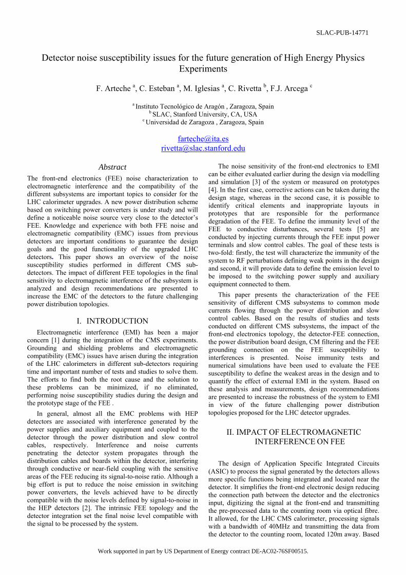
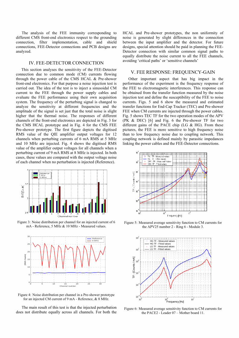
connection due to common mode (CM) currents flowing through the power cable of the CMS HCAL & Pre-shower front-end electronics. For that purpose a noise injection test is carried out. The idea of the test is to inject a sinusoidal CM current to the FEE through the power supply cables and evaluate the FEE performance using their own acquisition system. The frequency of the perturbing signal is changed to analyze the sensitivity at different frequencies and the amplitude of the signal is set just that the total noise is slight higher that the thermal noise. The responses of different channels of the front-end electronics are depicted in Fig. 3 for the CMS HCAL prototype and in Fig. 4 for the CMS FEE Pre-shower prototype. The first figure depicts the digitised RMS value of the QIE amplifier output voltages for 12 channels when perturbing currents of 6 mA RMS at 5 MHz and 10 MHz are injected. Fig. 4 shows the digitised RMS value of the amplifier output voltages for all channels when a perturbing current of 9 mA RMS at 8 MHz is injected. In both cases, these values are compared with the output voltage noise of each channel when no perturbation is injected (Reference).
Figure 3: Noise distribution per channel for an injected current of 6
mA - Reference, 5 MHz & 10 MHz - Measured values.
0 5 10 15 20 25 300
5
10
15
20
25
30
C hanne l num ber
[RM
S C
ount
s]
R e fe renc e8 M H z
Figure 4: Noise distribution per channel in a Pre-shower prototype for an injected CM current of 9 mA - Reference, & 8 MHz.
The main result of this test is that the injected perturbation does not distribute equally across all channels. For both the
HCAL and Pre-shower prototypes, the non uniformity of noise is generated by slight differences in the connection between the input amplifier and the detector. For future designs, special attention should be paid in planning the FEE-Detector connection with similar common signal paths to equally distribute the noise current to all the FEE channels, avoiding ‘critical paths’ or ‘sensitive channels’
V. FEE RESPONSE: FREQUENCY-GAIN Other important aspect that has big impact in the
performance of the experiment is the frequency response of the FEE to electromagnetic interferences. This response can be obtained from the transfer function measured by the noise injection test and define the susceptibility of the FEE to noise currents. Figs. 5 and 6 show the measured and estimated transfer functions for End-Cap Tracker (TEC) and Pre-shower FEE when CM currents are injected through the power cables. Fig. 5 shows TEC TF for the two operation modes of the APV (PK & DEC) [6] and Fig. 6 the Pre-shower TF for two different gains of the PACE chip (LG & HG). From these pictures, the FEE is more sensitive to high frequency noise than to low frequency noise due to coupling network. This coupling network is defined mainly by parasitic impedances linking the power cables and the FEE-Detector connections.
Figure 5: Measured average sensitivity function to CM currents for
the APV25 number 2 - Ring 6 - Module 3.
105 106 10710-3
10-2
10-1
100
101
102
Frequency [Hz]
TF -
[Cou
nts
/ mA
]
HG TF - Measured valuesHG TF - Fitted valuesLG TF - Measured valuesLG TF - Fitted values
Figure 6: Measured average sensitivity function to CM currents for
the PACE2 - Leader 07 – Mother board 11.

Additionally, it is important to remark that the sensitivity of the FEE is different for the two operation modes of the chip.
VI. GROUNDING CONNECTIONS EFFECTS The grounding of the FEE is important to ensure the
correct performance of the FEE. The grounding has to be designed to:
1. To minimize capacitive coupling between the structure and the sensitive areas of the FEE ( )(tn DF− ).
2. To create low impedance at the input of the power connector (in DM and CM) to avoid the external current interference flowing inside FEE electronics.
The implementation of these concepts and the way that they are implemented have important implications in the FEE immunity. As example, to show the effect of the FEE GND connection in the sensitivity of the FEE to CM currents, this section studies different methods of implementing the ground connection of the HCAL input power filter. The effects of the length and routing of the ground connection has been evaluated via CM current injection test. Fig. 7 shows the connection under study.
Figure 7: HCAL input power filter ground connection
During the test, the strap connection between the filter box and the read-out box (RBX), holding the HCAL electronics, is changed to study their influence on the FEE performance. This connection is made with a 15 cm long copper strap. The length and the routing of the strap connection to the RBX are changed. This modification produces a variation on the inductance of the ground connection. The results of three different layouts are presented.
• GND 1: The ground connection is done with a long strap. It is routed to the connection point as far as possible from the metallic structure of the RBX.
• GND 2: The second layout, the strap is routed to the connection point as close as possible to the metallic structure of the RBX following the shortest path to that point.
• GND 3: The third layout is similar to the second one, but a copper tape is used to fix the strap to the RBX (Fig. 7). This layout decreases the length of the strap to a minimum.
Figure 8 depicts the transfer function for the three configurations that have been studied. Results show the FEE susceptibility to CM currents for three different types of
ground connections. Based on these curves, the third layout (GND 3) is the best configuration to make the ground connection of the shield. Essentially this connection is characterized by the shortest and less inductive strap and produces the lowest value of ground impedance connection for the frequency range of interest. The system presents a higher rejection to shield currents because most of these currents can be by-passed from the RBX and hence they do not pass through the sensitive part of the FEE.
Figure 8: Channel 5 transfer function - Fitted values –
GND 1, GND 2 and GND 3 configurations.
For future designs, it is important to consider that the ground connection plays an important role in the FEE immunity. It defines the impedance between the FEE and the ground, setting the level of noise current that is capable of flowing inside the FEE metallic box. Based on this study, it is possible to define the main characteristics that should be followed for the ground connections:
• They should be short and flat. • Routing path should be as close as possible to the
metallic box.
VII. FEE TOPOLOGY - UNBALANCES The front-end electronics of the HCAL Forward Calorimeter (HF) is composed by photo-multipliers (PMT) located about 4 mts. from the sensitive amplifiers. This section studies the signal connection between each PMT and the respective amplifier to provide enough common mode rejection to avoid amplification of spurious signal due to the remote connection between grounds. The wide-band amplifiers used in the detector (QIE [7]) are very sensitive and the noise tolerated in the detector is just above the intrinsic thermal noise of the amplifier. The common mode rejection of the differential topology has been studied considering the circuit depicted in Fig. 9. The study is based on numerical simulation and the signal cables are modelled using Multi-conductor Transmission Line theory (MTL).
The influence of unbalances generated by the connection between the photodiodes and the FEE located 4 meters away is studied. Fig. 10 shows the common mode rejection to radiation noise of the HF FEE. It shows the performance of the HCAL FEE is decreased more by the different position of the cables on the cable tray than the capacitance unbalance of the photodiodes when the system is affected by electromagnetic radiated noise.

Rgnd
QIE ref.
Anode
Dy8
PMT
HV
Cc
QIE sig.
Figure 9: Forward HCAL Detector – FEE connection layout
It is important to consider for future designs that unbalances in the input signal circuit strongly increase the FEE noise susceptibility to EMI. The selection of specific components and the topology help to decrease unbalance effects. In this particular case, the HF immunity was improved by selecting a double twisted pair cable with a single braided shield
Figure 10: Comparison between the effect of the cable position and
the effect of the input capacitance unbalance.
VIII. FILTER IMPLEMENTATIONS The noise emissions in HEP experiments are mainly
dominated by the CM currents generated by switching DC-DC converters or by the radiated noise coupled to power cables. The CM current spectrum contains large amount of harmonic components from a few kHz up to hundreds of MHz. In general, this noise is difficult to cancel and may decrease signal-to-noise ratio of the FEE. The noise performance of the experiment can be improved either decreasing the impact of the environment noise (reducing the noise emitted by power supplies by installing filters at the output of the units or using shielded power cables) or increasing the FEE immunity by installing CM filters at the input power terminals of the FEE. CM filters protect the FEE from CM currents flowing through the power cables. A set of immunity tests have been carried out in CMS Tracker and HCAL FEE to evaluate the performance of CM filters installed at the input power terminals of the FEE.
Figure 11 depicts the sensitivity function of the HCAL FEE to common mode current flowing through the power cables, while Fig. 12 depicts the same function for the End-Cap Tracker (TEC). Those plots compare the immunity in case the FEE includes or not a CM filter at its input power
terminals. The HCAL FEE without CM filter is about 14dB more sensitive than the FEE with filter and for TEC the results depicted in Fig. 11 shows a general improvement between 12-30 dB, when a filter is installed at the input power terminals. The filter has been implemented with 3 surface mount capacitors of 1µF.
Figure 11: CM transfer function of HCAL-FEE with and without
CM filter at input power terminals.
105
106
107
10- 5
10- 4
10- 3
10- 2
10- 1
100
F req uency [H z ]
TF
- [ C
ount
s /
mA
]
CM T F - P K A P V 632 - C M F ILTE R CM T F - P K A P V 632
Figure 12: CM transfer function of TEC-FEE with and without CM
filter.
It is clear that it is necessary to protect the FEE from the common mode noise currents by avoiding these currents can flow through the sensitive paths inside the FEE, deteriorating the performance of the system. An improvement in the CM immunity in the range of 10-20dB is achieved when CM filters are included at the input power terminals. Further improvements are no possible, because the CM filter cannot be implemented with inductors based on magnetic materials. The high magnetic field in the central area of LHC detectors excludes the use of magnetic materials.
IX. FEE SYSTEM DESIGNS This section analyzes the performance of different CMS
tracker subsystems. All tracker subsystems are configured using the same FEE electronics: silicon micro-strip detector, the APV-25 amplifier and the optical driver. These devices are integrated following different geometries depending upon the location in the Tracker (TIB, TOB or TEC).
Part of the tests performed on the CMS tracker consisted in CM noise injection through the power cable. The subsystems measured were the Tracker Outer Barrel (TOB) and the Tracker End Cap (TEC). Fig. 13 shows the immunity function to CM noise currents of TEC and TOB FEE setting

the APV in peak mode. The immunity of TEC system is much higher than the TOB immunity to CM currents flowing into the FEE through the power cable. Despite that both sub-systems use the same basic electronic devices; there is a large difference in the interference rejection. The main difference in both designs is the power distribution within the FEE trough the interconnection board (ICB). The TEC subsystem includes a ground plane in the ICB that shields the EM fields generated by power currents. This EMI is coupled by near-field to the strip detector. The TOB ICB design does not include that shielding.
106 10710
-3
10-2
10-1
100
101
F requenc y [Hz ]
TF -
[cou
nts
/ mA
]
P relim inary TO B - TF P KTE C - TF P K
Figure 13: CMS TOB and CMS TEC sensitivity to CM currents
flowing through the power cable.
Routing the power distribution and slow control signal within the subsystem using proper shielding has a strong impact in the FEE susceptibility. A ground plane in the ICB design helps to decrease the length of ground connections and confine within the board the EM fields generated by the DC power distribution. These considerations in the ICB design improve the immunity of the FEE.
X. SLHC IMPLICATIONS Up-grades for the central detector in both the CMS and the
Atlas experiments require defining new schemes for the DC power distribution. The power schemes proposed can be grouped into: Serial Power Distribution System and DC-DC switching power converters. Both schemes have advantages and disadvantages, but the viability of each of them will be closely associated to the FEE design. • DC-DC switching power converter based: Aspects like
CM noise and radiated noise are very important. It is important to pay attention to power distribution boards, ground planes and CM filters to ensure the compatibility between FEE and power system.
• Serial power Distribution System: Noise aspects (CM and radiated noise) associated to the Detector-FEE connection will be crucial to guarantee good performance due to the lack of global ground.
In both cases, it will be crucial to conduct EMC studies to be able to improve the noise immunity of the front-end electronics to be compatible with the noise emitted by the power converters. The compatibility between PS and FEE can only be achieved minimizing both the radiated and conducted noise emitted by the power supplies and the sensitivity of the FEE to EM noise.
XI. CONCLUSIONS EMC studies based on numerical simulations and tests
have been conducted on prototypes of CMS sub-detectors to characterize the FEE against EM interference. A summary of these studies, including the impact in the FEE susceptibility of FEE topology, Detector-FEE connection, power distribution board design and CM filter, and FEE grounding connection is presented. These tests have been remarkable important to evaluate weak areas of the system and the impact of the design in the FEE noise immunity. Similar procedures will be valuable to assess the electromagnetic compatibility between the FEE and power supplies in critical sub-detector up-grades for the LHC calorimeters.
XII. ACKNOWLEDGMENT The authors would like to thank to Dr. Peter Sharp from
Imperial College/CERN for helping us during the development of these studies. F.A., C.E. and M.I. would like to thank to Instituto Tecnológico de Aragón (ITA), Zaragoza, Spain, specially to Dr. J. L. Pelegay, head of Grupo de Investigación Aplicada (GIA) for the support of this work. Finally, one of us (C.R.) wants to thank to US Department of Energy for the support of this work, under contract DE-AC02-76SF00515.
XIII. REFERENCES [1] F. Arteche, C. Rivetta and F. Szonsco, “Electromagnetic Compatibility Plan for the CMS Detector at CERN ”, Proc. of 15th Int. Zurich Symposium on EMC, February 18-20, 2003, Zurich, Switzerland, pp. 533-538. [2] F.Arteche and C. Rivetta, “EMI Filter Design and Stability Assessment of DC Voltage Distribution based on Switching Converters”, Proceedings of Workshop on Electronics for LHC Experiments, LEB 2001, Vol 1, pp353-357, Sept. 2001 [3] F. Arteche and C. Rivetta, "Noise Susceptibility Analysis of the HF Front-End Electronics for the CMS High -Energy Experiment", Proc. of IEEE Int. Symposium on EMC. August 2003, Boston, USA, pp. 718-723. [4] F. Arteche and C. Rivetta “EM Immunity studies for front-end electronics in high-energy physics experiments”, Proc. of Int. Symposium on EMC, EMC Europe 2004. pp. 533-538, Eindhoven, The Netherlands, September 2004. [5] F.Arteche and C. Rivetta, “Electromagnetic Compatibility Test for CMS experiment”, Proceedings of Workshop on Electronics for LHC Experiments – LECC 2002, Vol 1 , pp191-196, September 2002. [6] M. Raymond, et. al., "The APV25 0.25 µm CMOS readout chip for the CMS Tracker", Proc. IEEE Nuclear Science Conference, October 2000, Lyon, France, pp. 9/113 - 9/118 [7] T. Zimmerman, J. R. Hoff, “The Design of a Charge-Integrating Modified Floating-Point ADC Chip”, IEEE JSSC, Vol. 39, No. 6, June 2004.