development and analysis of a compact dual-band...
TRANSCRIPT
CHAPTER 3
• Methodology •
This chapter describes the experimental and simulation facilities utilized to
characterize the behavior of the coplanar waveguide and final antenna configuration.
The coplanar wavcguide and proposed antenna are fabricated using the in-house
photolithography facility. The antenna characteristics such as return loss, radiation
pattern and gain are measured using vector nct\vork analyzer and associated
instrumentation. Theoretical analysis of the offset fed coplanar waveguide and
antenna are done using in-house developed MATLAB based FDID codes. The
Method of Moment based I E3D EM solver and FEM based TIFSS are also
employed for simulation.
-CREMA, CUSAT

Melhodology 85
3.1 Fabrication method
'l1,e offset fed coplanar wa .... eguide and the printed coplanar an tenna arc
fabricated on different substratc materials using standard photolithography facility
a\'ailablc in the laboratory. Photolithography method gives good accuracy for the etched
patterns. ' I"is is ,"cry critical when the frequency o f operation of the dC"icc is in higher
microwa'"c bands. The step by step process for the fabrication is \"ery simple and
illustrated in Fig. 3. 1 below.
D
Ph<>I".... .. , ho.rdm.;" do. l:V <If>Oot<I .,. ..
..... , ..... ·1"""'·"1' on ,h. ,ubu,.", .~,
' '''''''-1'.0''''''
Fig. J. I 511:p by Step proc"$S uwolv"d In I'M I" luhogr;&pnlC pro«~s
CREMA. CUSAT
86 Chapter 3
The computer aided design of the geometry is initially made and a negative
mask of the geometry to be generated is printed on a butter paper. A double sided
copper clad lamination of suitable dimension required for the antenna is cleaned very
well and dried. Any dust or impurities on it will produce small discontinuity on the
copper traces etched on the substrate. This will shift the resonant frequency from the
predicted values, especially when the operating frequency is very high. Now, the negative
photo resist material is applied on copper surfaces. It is then exposed to ultra violet
radiation through the mask The layer of photo-resist material in the exposed portions
hardens. Now the board is immersed in developer solution for few minutes. The
hardened portions will not be washed out by the developer solution. The board is then
dipped in the dye solution in order to clearly view the hardened photoresist portions on
the copper coating.
The unwanted copper traces now exposes after the developing phase is to be
etched off to get the required antenna geometry on the substrate. Ferric Chloride (Fea3)
solution is used for this purpose. Fe03 dissolves the copper parts except underneath the
hardened photo resist layer after few minutes. The laminate is then cleaned carefully to
remove the hardened photoresist using acetone solution.
3.2 Microwave subst:rates
Selection of substrates ID ffilcrowave circuits IS very important. Low loss
substrates are very important at microwave bands. As frequency of operation increases,
the loss tangent of the material used for substrates slightly increases, which in tum
Development and Analysis of a Compact Dual-band Coplanar Antenna

Methodology 87
adversely affect the efficiency of the antenna. The power handling capability of the
antenna depends on the substrate materials also. At high power certain substrate
materials cannot withstand. A variety of substrate materials are available in the market.
Flexible substrate materials are also available, so that the antenna can be mounted on
curved surfaces. The selection of dielectric constant of the substrate depends on the
application of the antenna and the radiation characteristics specifications. It is worth
noting that surface waves will be excited in high dielectric constant substrates. This will
generate spurious radiations in unwanted directions from the antenna. In this thesis
importance is given to compactness of the antenna structure. Table 3.1 shows the details
of the substrates used in the thesis.
SI. No.
2
TABLE 3.1 DETAILS OF 'fl-lE MICROWAVE SUBS1RATES U;r:D IN 'IHE lHESIS
Substr'J.tt
FR4
RTdlll'oid
Relative dielectric constant, loss tangent and dielectric thickness
E,=4.4 tan, 0=.02, h=1.6 mm
(,=2.2, tan 0=.002, h=1.S mm
Prototype of offset fed coplanar waveguide and antennas were fabricated on FR4 and
RT duroid substrates.
3.3 Experimental characterization setup
Antenna characteristics such as return loss, radiation pattern and gain are
measured using the HP8510C and associated setup. The indegeneously developed
CREMA SOFT is used for the automatic measurement of the radiation properties using
HP 8510C Network analyzer. The important systems used for the antenna
-CREMA, CUSAT
88 Otapter3
characterization are Vector network Analyzer, Anechoic ClJ.amber, Automated turn table
etc.
3.3.1 HP 8510C Vector Network Analyzer
This is a sophisticated Vector Network Analyzer (VNA) from Hewlett
PackarU with time domain and frequency domain operation capability [1]. The
microprocessor based system can measure two port network parameters such as S11, S12,
S21 and S22 very accurately. The in built signal processing algoritluns of the network
analyzer process the transmit and receive data and finally displays the measured values in
many plot fonnats. The schematic of the VNA is shown in Fig. 32.
Develovment and Analysis of a Compact Dun/-band Coplanar Antenna

Methodology
Aa'~". ~ .. d .. T,. I'''''
1IP85148
~ ____ +-~r·'·m'''''I~'()
HP 836516 Syn ' ltcli~ed _ cere'
HP"
Fig. 1.2 Schcnutlc dtagrun of the 1IP8;IOC vector netwOrk an:&!y7.cr setup used for thf' .:;har:acteriunon o f the antcnnu
89
The network analyzcr consists of a microwave generator, S parameter test
set, signal processor and the display unit as illustrated in Fig. 3.2. The synthesized su'ccp
generator HP 83651B uses an open loop YIG tuned element to generate (he RF
stimulus. I t can synthesize frequencies from 10 MHz (0 50 GHz. The frequencies can be
set in step mode or ramp mode depending on (he required measurement accuracy.
The antenna under test (AUI) is connected to the port of the S-paramctcr
tCst set IIP8514B and the forward and reflected power at the measurement point is
separated and down converted to 20MlIz using frequency down converter. It is again
90
down comwlcd to lower frl'qucnc)' and processed in the I IP851 OC processing unit. All
the systems dis(u~:;('d abovc arc interconnected using I IPIB bus. A computer interfaced
to [ht, sy:Hcm is used for coordinating the whole operation remotely. r.,.,leasurcmcm data
can be S3\Td on a storage medium using it.
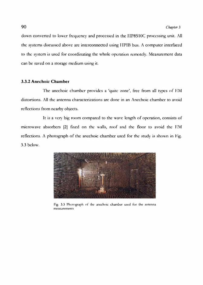
3.3.2 Ancchoic Chamber
The anechoic chamber provides a <quLte zone', free from all types fir EM
distortions. AU the antenna characterizations arc done in an Anechoic chamber to 3,'oid
reflections from nearby objects.
If is a very big room compared to the wan' length o f operation, consists of
ffilCroW3\"C absorbers [21 fixed on the walls, roof and the floor to avoid the EM
reneerion s. A photograph of the ancchoic chamber used for [he study is shown in Fig.
3.3 below.
PIg. ) .3 Pho t"gr.lph (>1 the dncchnic ch.lmb~'I" uSl'd to r the :UHenna nlr;t5urcment~
Methodology 91
The absorbers fixed on the walls are highly lossy at microwave frequencies.
They have tapered shapes to achieve good impedance matching for the microwave
power impinges upon it. The chamber is made free from the surrounding EM
interferences by covering all the walls and the roof with aluminiwn sheet.
3.3.3 Turn table assembly for far field radiation pattern measurement
The turn table assembly consists of a stepper motor driven rotating platfonn
for mounting the Antenna Under Test (AUI). The in-house developed microcontroller
based antenna positioner STIe 310e is used for radiation pattern measurement. The
main lobe tracking for gain measurement and radiation pattern measurement is done
using this setup. A standard wideband horn (1-18GHz) is used as receiving antenna for
radiation pattern measurements. The in-housed developed automation software 'Crem:t
Sift' coordinates all the measurements.
3.4 Measurement procedure
The experimental procedures followed to detemUne the antenna
characteristics are discussed below. The network analyz.er in real practice is connected to
large cables and connectors. The connectors and cables will have its losses associated at
higher microwave bands. Thus the instnunent should be calibrated with known
standards of open, short and matched loads to get accurate scattering parameters. There
are many calibration procedures available in the network analyz.er. Single port, full two
pon and 1RL calibration methods are usually used. The two port passive or active
device scattering parameters can be accurately measured using 1RL calibration method.
CREMA, CUSAT
92 Chapter 3
Return loss, VSWR and mput impedance can be characterized usmg single pon
calibration method.
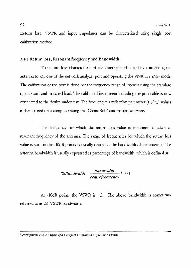
3.4.1 Return loss, Resonant frequency and Bandwidth
The return loss characteristic of the antenna is obtained by connecting the
antenna to anyone of the network analyzer pon and operating the VNA in s 11/ S22 mode.
The calibration of the pon is done for the frequency range of interest using the standard
open, shon and matched load. The calibrated instrument including the pon cable is now
connected to the device under test. The frequency vs reflection parameter (511/ S22) values
is then stored on a computer using the 'Crema Soft' automation software.
The frequency for which the return loss value is minimum is taken as
resonant frequency of the antenna. The range of frequencies for which the return loss
value is with in the -lOdB points is usually treated as the bandwidth of the antenna. The
antenna bandwidth is usually expressed as percentage of bandwidth, which is defined as
bandwidth %Bandwidth = * 100
centrefrequency
At -lOdB points the VSWR is -2. The above bandwidth is sometimes
referred to as 2:1 VSWR bandwidth.
Development and Analysis of a Compact Dual-band Coplanar Antenna
MethodoiogJ) 93
3.4.2 Far field radiation pattern
The measurement of far field radiation pattern is conducted in an anechoic
chamber. The Aur is placed in the quite zone of the chamber on a turn table and
connected to one pon of the network analyzer. A wide band horn is used as a transmitter
and connected to the other pon of the network analyzer. The turn table is controlled by
a STIe positioner controller. The automated radiation pattern measurement process is
coordinated by the 'Crr:ml Srft' software in the remote computer.
In order to measure the radiation pattern, the network analyzer is kept in
S21/S12 mode with the frequency range within the -lOdB return loss bandwidth. The
number of frequency points are set according to the convenience. The stan angle, stop
angle and step angle of the motor is also configured in the 'Crr:ml Sift'. The antenna
positioner is boresighted manually. Now the TI-IRU calibration is perfonned for the
frequency band specified and saved in the CAL set. Suitable gate parameters are
provided in the time domain to avoid spurious radiations if any. The Crr:ml Sift will
automatically perfonn the radiation pattern measurement and store it as a text file
3.4.3 Antenna Gain
The gain of the antenna under test is measured in the broadside direction.
The gain transfer method using a standard gain antenna is employed to determine the
absolute gain of the Aur [3-4]. The experimental setup is similar to the radiation pattern
measurement setup. An antenna with known gain is first placed in the antenna positioner
and the 1HRu calibration is done for the frequency range of interest. Standard antenna
is then replaced by the Aur and the change in 521 is noted. Note that the Aur should
!:: aligned so that the gain in the main beam direction is measured. This is the relative CREMA, CUSA T

94 Chapier 3
gain of the antenna with respect to the reference antenna. The absolute gain of the
antenna is obtained by adding this relative gain to the original gain of the standard
antenna.
3.5 lE 3D Electromagnetic Simulator
The IE3D Electromagnetic simulator works based on Method of Moment
[5]. TIns full wave simulator is capable of simulating microwave circillts such as
microstrip circuits, printed antennas and some types of wire antennas. There is no
limitation on the size and shape of the antennas to be simulated. The OJRVIEW post
processor of IE3D provides colorful 3D and 2D display of current distribution and
radiation patterns. aJRVIEWalso provides complete information on the directivity,
return loss, efficiency, axial ratio, 3 dB beam width, and RCS. Most field solvers assume
infinite ground planes in solving circuit and antenna problems. In many microwave
applications one may not be able to find a big ground plane. Therefore, infinite grOlmd
plane assumption is not applicable. IE3D is able to model structures with finite ground
plane.
The different port types available in IE3D are very useful for microwave
circuit simulators to excite the devices according to the convenience of the designer.
G>planar wave guide ports, probe feed are widely used in IE3D. In this thesis the study
of the radiation pattern, gain and efficiency of the coplanar wave guide with corner feed
is done using IE3D. The edge port schemes suitable for coplanar wave guide
applications are used in the study. The first step in IE3D simulation is to define the
De'l,elopment and Analysis of a Compact Dual-band Coplanar Antenna

Methodology 95
material parameter such as substrate thickness, dielectric constant, and metallic
properties in MGRID window. Then draw the required circuit geometry in MGRID.
The simulation setup in the window is then used to specify the frequency range of
simulation, number of frequency points etc. The simulation results are available in
MODUA window available with IE3D.
3.6 HFSS: 3D Electromagnetic simulator
HFSS utilizes a 3D full-wave Finite Element Method (FEN!) to compute the
electrical behavior of high-frequency and high-speed components [6]. With HFSS one
can extract the parameters such as S, Y, and Z, visualize 3D electromagnetic fields (near
and far-field), and optimize design performance. An important and useful feature of this
simulation engine is the availability of different kinds of port schemes. It provides
lumped port, wave port, incident wave scheme etc. The accurate simulation of coplanar
wave guides and microstrip lines can be done using wave port.
In this thesis some parts of the investigations are done using HFSS. The
optimization algorithm available with HFSS is very useful for antenna engineers to
optimize the dimensions very accurately. There are many kinds of boundary schemes
available in HFSS. Radiation boundary and PML boundary are the important are widely
used in this work The vector as well as scalar representation of E, H, J values of the
device under simulation gives a good insight in to the problem under simulation.
The first step in simulating a system in HFSS is to define the geometry of
the System by giving the material properties and boundaries for 3D or 2D elements
-CREMA, CUSAT

96 Chapter 3
available in HFSS window. The suitable port excitation scheme is then given. A radiation
boundary filled with air is then defined surrounding the structure to be simulated. Now,
the simulation engine can be invoked by giving the proper frequency of operations and
the number of frequency points. Finally the simulation results such as scattering
parameters, current distributions and far field radiation pattern can be displayed.
Development and Analysis of a Compact Dual-band Coplanar Antenna

Methodology 97
References
-
1. HP8510C Network Analyzer operating and programming manual, Hewlett
Packard, 1988.
2. Design, Development and Perfonnance Evaluation of an Anechoic d1amber for
Microwave Antennas Studies, E. J. Zachariah, K. Vasudevan, P. A. Praveen
Kumar, P. Mohanan and K. G. Nair, Indian Journal of Radio and Space Physics,
Vo. 13, February 1984, pp. 29-31.
3. C A. Balanis, Antenna Theory: Analysis and Design, Second Edition, John
Wiley&Sons Inc. 1982
4. John D. Kraus, Antennas Mc. Graw Hill International, second edition, 1988
5. IE3D User's manual, Release 7, Zeland Software Inc. December 1997
6. HFSS User's manual, version 10, Ansoft Corporation, July 2005
CREMA, CUSAT