development and manufacture of the microchannel plate … · development and manufacture of the...
TRANSCRIPT

[LE ~ 41
Center for Night Visionand
Electro-Optics P
DEVELOPMENT ANDMANUFACTURE OF THEMICROCHANNEL PLATE
(MCP)
byWalter B. Morrow, Jr., John Rennie,
and William Markey
February 1988
Approved for public release; distribution unlimited.
DTIC.LECTE
S D
FORT BEL\'OIR, V!RGINIA 220rj0-5677
88 3 16 106I~. I .g.
AMSEL-RD-NV-D (DTIC-HAC/9 Jun 88) (702-3b) 1st EndSUBJECT: Technology Screening of Unclassified/UnlimitedReports (CNVEO Rept. AMSEL-NV-TR-0064)
Headquarters, US Army Communications-Electronics Command,Center for Night Vision and Electro-Optics, ATTN: AMSEL-RD-NV-D, Fort Belvoir, VA 22060-5677
FOR: Defense Logistics Agency, Defense Technical InformationCenter, ATTN: DTIC-HAS, Cameron Station, Alexandria, VA22304-6145
1. CNVEO has reviewed the report cited in the referencedletter and the cited MCTL References paragraphs 4.1.3(4d)and 7.3.3. In addition CNVEO has reviewed the issue withthe PMO-NVD and Varian Associates.
2. The MCTL (Oct 1986) sets forth as militarily criticaltechnology three items which are relevant to the CNVEOReport AMSEL-NV-TR-0064. These items are a. (U) ChemicalProcessing of the Multiple Fibre Wafer; b. (U) HydrogenFiring and Vacuum Bake of the Multiple Fibre Waver; and c.(U) Deposition of Ion Barrier Films less than or equal to50 nanometers in thickness. The subject CNVEO reportconsists of two main sections, the first being a very muchsimplified and qualitative outline of the general type ofsteps required to manufacture a microchannel plate. Thesesteps are generic and gleened from 1967-1971 vintage materialwhich has been in the public domain since that time. IonBarrier Films are mentioned only to state without embellish-ment, the generally known fact that such films may beapplied to an otherwise finished microchannel plate. Micro-channel plates are currently manufactured by British, French,
and Dutch interests and to some extent in the Eastern Block.The material is also wholly lacking in all the critical [ ..information such as chemical composition, temperatures,times/schedules, degree of vacuum or pressure etc., withoutwhich the process cannot be accomplished. The second partof the report consists of a reproduction of a VarianAssociates Pamphlet MCP-2819B which is a commercialmarketing type pamphlet published initially in 1975 with Ilat least three subsequent reprintings. It deals only withtypical performance parameters. Similar or identicalmaterial to that published in the CNVEO report has appearedin standard technical books and has been the subject of manyprofessional/technical papers presented around the world.Some 20,000 copies of the Varian pamphlet itself have beenprinted and distributed world wide.
nil

AMSEL-RD-NV-DSUBJECT: Technology Screening of Unclassified/UnlimitedReports (CNVEO Report AMSEL-NV-TR-0064)
3. Based upon the above it is the considered opinion ofCNVEO that there exists no basis for changing the "unclassi-fled/unlimited" classification of the subject report. Thisreport has been intended by CNVEO to provide a simplistictutorial for those who become or may become involved inthe area of night vision systems, who are not necessarilyengineers or scientists, yet who require some basic under-standing of the technologies involved. The dedicatedtechnologist can readily pursue the subject to much greaterdepth in the published literature.
4. Questions on the above should be directed to Mr. WalterB. Morrow, Deputy Director Technical Support Division onAUTOVON 354-5694 or Commercial 66 4 - 5 6 9 4.
RUDOLF G. B ERActing DirectorCNVEO
DEPARTMENT OF THE ARMYCENTER FOR NIGHT VISION AND
ELECTRO-OPTICSFORT BELVOIR, VIRGINIA 2206-5677
AMNIý-I-rSPENALTY FOR PRIVATE USE. S300
Defense Logistics AgencyDefense Technical Information CenterATTN: DTIC-HASCameron StationAlexandria, VA 22 3 0 4- 5 67 7
2

UnclassifiedSECURITY CL.ASSIFICATION OF 7-- S RA
REPORT DOCUMENTATION PAGE I 0O0 7408
ta REPORT SECuRITY CLASSiFCArTON To RESTRIC7TVE VIARC(NC.S
Unclassified NofleI&. SECURITY CLASSIFICATION AU'iORIT'r 3 01STRu3UTiON AVA-LABILITY OF REPOR4T
2b. DICLASSIFICATIONiOOWNGRADING SCHEDULE Approved for public release; unlimited distribution.
4. PERFORMING ORGANIZATION REPORT NUMBER(S) 5. MONITORING ORGANIZATION REPORT NUMBER(S)
AMSEL-NV-TR-0064
6.. NAME OF PERFORMING ORGANIZATION 6b. OFFICE SYMBOL 7&. NAME OF MONITORING ORGANIZATION
Electro-Optics (CNVEO) IAMSEL-RD-NV-TSI6C. ADDRESS (CiMy State. and ZIP Code) 7b ADDRESS XCity, State, and ZIP Code)
Fort Belvoir, VA 22060-5677
8.. NAME OF FUNDING, SPONSORING r8b OFFICE SYMBOL 9 PROCUREMENT iNSrRu~v,% E',j7.NFCA'ON %UMBER
ORGANIZATION j(if applicable)
St. ADDRESS (City. State, and ZIP Code) TO SOURCE OF FUNDING INUMSERS1PROGRAM IPROJECT TASK IWORKZ UNITELEMENT NO INO NO. rACCESSION NO
11. TITLE (include Security Classification)
DEVELOPMENT AND MANUFACTURE OF THE MfICROCHANNEL PLATE (MCP) (U)
12. PERSONAL AUTHOR(S)Walter B. Morrow. Jr..-John Rennie, William Mlarkey___________________
13a. TYPE OF REPORT 13b TIME COVERED !4 DATE OF REPORT (Year, AofnthOay) 15 PAGE COUNT.Final IFROM 1962 TO 1988 February 1388 29
16. SUPPLEMENTARY NOTATION
17 COSATi CODES 18 SUBJECT TER.MS (Continue on reverse if necessary ania identify1 by block number)IED GROUp I SUB-GROUP M Ai & c W#ri-4oSr ~ t'~~FIELD c ladding glass, etched core approach; boule fusion; chemical etching:,
h rdrogen firing; image inesfe be; electron scrub-, G&At IS&19. ABSTRACT (ContiA~ onrverse of necessary and identify by block number)
This technical report contains an overview of the .Jevelopment and production ofa critical night vision electronic device, the microchannel multiplier ormicrochannel plate (MCP). Technological challenges and manufacturingprocesses for the second and third generation image intensifier tube systems areoutlined including materials selection, rhermo-mechanical processing, chemicalprocessing, mechanical processing and assembly, and cleaning, chemicalactivation, and electron scrub. Also contained in this report are three figureswhich chart MCP research and development investment/payoff, unit costreduction curve for second generation, and estimated production costcomparisons of years 1977 and 1987. The Appendix contains Varian Associates'pamphlet M.CP-2819B, Applications for Vicrochannel Platlec(,-.,ký',,
0O Form 1473, JUN 86 .revrous editcions are obsolere SECI.A'y CLASSIFiCAT ON OF -Hi P'AGE_U'nclassi fied
PREFACE
This report provides a brief overview of the development of the microchannel electron multiplier or
microchannel plate (MCP) with emphasis on the technological challenges to produce this critical
device. The MCP is one of the most physically complex electronic devices in mass production
today and is the critical component enabling the Army to deploy more than 150,000 low cost night
vision systems. Applications span all of the military services and include man-carried, combat
vehicle and aviation applications, both fixed and rotary wing. Emphasis is also placed on the need
for well structured, fully supported, and funded developmental programs where technological
challenges and barriers are overcome systematically, thus achieving the desired goals of full
performance, low cost production, and high reliability with attendant low operational and sustaining
cost.
The Appendix contains Varian Associates, Light Sensing and Emitting Division, Palo Alto, CA,
pamphlet #MCP-2819B, Applications for Microchannel Plates.
Aceession For
NTIS GRA&I
DTIC TAB1Unwir ouix adJust ificAti1or-._
COPYBy\.INSPECTE) DiDstributi on/
A.vailability en"168
Ave.itl and/or... Dist Special
I1 7i

TABLE OF CONTENTS
Section I. Introduction ....................................................................................................... I
Section II. MCP Development and Manufacturing Challenges ...................................... 2
Section III. Summary of MCP Fabrication ...................................................................... 5
Section IV. Investment/Payoff Considerations ................................................. 7
Appendix: Applications for Microchannel Plates, Varian Associates, Palo Alto, CA,#M CP-2819B .............................................................................................. A -1
iv
SECTION 1. INTRODUCTION
By mid year 1987, the US Army procured and deployed more than 150,000 second generationimage intensifier systems. These include the AN/PVS-4 small starlight scope, AN/TVS-5 crewserved weapon sight, AN/PVS-5 night vision goggles, and third generation high performanceAN/AVS-6 aviation night vision goggles. By 1990, more than 300,000 such systems are expected tobe deployed to Army, Air Force, Navy, and Marine Corps units worldwide. These systems are allcharacterized by significantly smaller size, lighter weight, higher performance, and lower cost thantheir first and zero generation counterparts. The very popular goggles were in fact nottechnologically possible in first and zero generation. The unique device which has made thispossible is the continuous channel electron multiplier, better known as the Microchannel Plate(MCP). The MCP development was supported by a long range commitment by the Army toresearch and investment in the technology during the years 1962-1985. Prototype image tubesfabricated in the early 1970s had MCPs costing several thousand dollars. Today, high performanceMCPs cost less than $200 each in quantity (refer to Section III). This was accomplished over adecade and a half in which the aggregate inflation was nearly 300%. Low cost efficient massproduction of MCPs is something of a technological miracle considering the lengthy and complexprocess.
There are a number-of lessons to be learned from the Anny's program for second generation imagetube and MCP development. These include, as a minimum, .the following:
* Key component development continued throughout the development cycle for end itemhardware.
* Detailed specifications were generated for both MCPs and tubes and were evaluated in-houseagainst these specifications.
* Simulated test apparatus were designed, fabricated, and tested in-house as vehicles to checkcontractor performance and recommend positive changes. In fact, the Center for Night Visionand Electro-Optics (CNVEO), through intense in-house research, was often in the forefront andtransferred vital data, particulary processing methods, to industry.
* Attempts at accelerated development did not succeed schedule wise, indicating that theapplication of brute force cannot be substituted for sound scientific methodology.
• The worldwide deployment of thousands of low cost second and third generation imageintensifier systems was the result of a logical and well thought out effort, Advanced

Development, Engineering Development, pre-production preparation manufacturing, materials, and
technology programs (MM&Ts), facility contracts, and a plan to insure a healthy degree of
legitimate competition, i.e., Educational Buys and Qualified Sources for critical items/components.
SECTION II. MCP DEVELOPMENT AND MANUFACTURINGCHALLENGES
The concept of a continous channel electron multiplier was developed near the end of 1950. Theinvention was that of G.W. Goodrich of the Research Laboratories Division, Bendix Corporation.The intrinsic property of glass as a defacto amorphous super-cooled fluid subject to tensile creep atrelatively low temperatures lent itself readily to the development of the MCP as we know it today.
Early experiments with brittle insulators such as polycrystalline isotropic ceramics were neversuccessful for this application. Even with glass, several approaches were explored. The principalapproaches were the hollow core and etched core MCPs. The hollow core approach, while viable in
principal, has never achieved economically satisfactory manufacturing yields. Thus today, only the
etched core approach remains. An understanding of the challenges to be overcome in the
development and manufacture of the modem MCP can best be done in the context of themanufacturing process itself; therefore, the more significant steps in that process are reviewed. Ingeneral, the technological challenges have been in materials selection, thermo-mechanicalprocessing, chemical processing (etching, hydrogen firing), mechanical processing and assembly,and finally, cleaning, chemical activation, and electron scrub.
Selection of core and cladding glass material is the first challenge. The cladding glass must be ahigh lead concentration glass which can be hydrogen fired to produce a conductive layer on theinside of the tube. Approaches which would attempt to apply a conductive coating directly to theinside of channels were infeasible due to the small channel diameter (8-9 microns) which was
ultimately required. The core glass must match the thermal expansion coefficient of the claddingglass; otherwise, the two could not be processed at temperature. A mismatch prevents the fusion of
core and cladding glass and results in improper preparation of the cladding glass surface andfracturing of the cladding glass itself. Finally, the core glass must be subject to etching while the
cladding glass must remain impervious to the etching material. After much research, it wasdetermined that the ideal cladding glass was Coming 8161, containing a high concentration of lead
and requiring rubidium as a catalyst in the manufacturing process. However, Corning's supply ofthis glass was limited and access to rubidium was severly limited by a trade embargo againstRhodesia, the principal supplier. This forced the industry to seek alternative ways of producing the
8161 glass or develop an equivalent. This was accomplished through an intense and structured effortby the CNVEO through in-house research and contracts for material research, manufacture of thetest MCPs, and testing in image tube structures. The problem was fully resolved in just 18 months.
2I
II M I
The next three steps are drawing and stacking steps in which initially the core and cladding glass areconcentrically drawn to a very thin diameter. Both glasses must have the same temperature/flowcharacteristics. In the first step, single glass rods are drawn down to a specified diameter. In thesecond step, the singles are stacked and fused. This requires careful temperature control to affectuniform fusion without inducing excess flow or geometric distortion. Finally, the third step is themulti-draw step requiring precision temperature control and very exact control of the tensile loadapplied to effect the draw. The result of these three steps is to obtain a center-to-center spacingbetween channels of 12 microns and individual channel diameters of 8-9 microns uniform over aneffective plate area of 18-25 millimeters.
The next step requires mechanical assembly of drawn multibundles into a solid rim followed bypressing and fusing into a boule. Boule fusion is critically dependent upon process time and timing,and precise control of both pressure and temperature. Because of the intrinsic flow/creep propertiesof glass, this step, if not precise, can lead to excessive flow, nonuniform fusion, and geometricdistortion in the boule. The ability to do this relates in no small way to the intrinsic uniformity ofthe glass tubing used at the start of the process.
Having fabricated a successful glass boule, it is now necessary to slice the boule transversly ornearly so at a small bias angle in the order of 5 to 80 and with a resulting plate thickness of just over20 mils (.020 inch) allowing for subsequent grinding and polishing. The thickness determines theelectron gain/saturation characteristic of the MCP and so these steps must be precise. While theboule itself is robust, the single MCP wafer is mechanically delicate and easily destroyed in thesesteps. The grinding and polishing step, though outwardly simple for solid glass, is a delicate processhere, since it is necessary to prevent smearing of cladding glass into the core glass. Failure here canresult in the loss of the plate or produce defective channels in subsequent steps.
At the next stage, chemical etching occurs to remove the core glass and leave open channels. Theetch must be controlled since this process not only removes the core glass, but treats the surface ofthe cladding glass/core glass fusion boundary to produce a secondary electron emission surface withthe necessary properties. At the same time, it is critical that all core glass residues and etchingmaterials be removed; otherwise, blocked and defective channels will occur having very undesirableproperties.
Having successfully etched and cleaned the MCP, hydrogen firing is next. This serves to reduce theLead Oxide (PbO) distributed on the inner surface of each channel to conductive metallic lead. Thedegree of lead oxide reduction obtained determines the conductivity of the inner surface, and thestability of this parameter is a critical function of the time and temperature profiles used in hydrogenfiring.
3

The MCP now passes through the step where electrical contacts are vacuum vapor deposited across
the front and back surface areas. The adherence of the contact film is dependent upon the quality
and effectiveness of the cleaning, etching, and firing steps in the previous paragraphs. In addition,
the choice of electrode material is critical in that thermo-mechanical properties must again be
matched in order to insure long term operational stability. The evaporation technique itself is a
complex process requiring careful control obtainable only through fully automated processes.
NOTE: Various tests are performed at numerous times during the entire process. Often these tests,
like the processes themselves, require exacting and unique jigs, fixturing, control mechanisms, and
analytical aids.
The next step in the process is typical of the many requiring special jigs and fixtures. This is the
assembly of the MCP into an image intensifier tube body. Special assembly techniques are required
and ultra-clean facilities are used continuously. It is critical here that MCP electrodes and tube body
electrodes meet and match, guaranteeing electrical contact. Failure here can impact tube gain,
noise/background characteristics, and loss of stability due to field emission and arcing/corona
effects.
In the final step of the second generation type tube, the MCP is outgassed while in the tube. This is
accomplished by a very precisely controlled electron scrub. This has been one 6f the most
challenging areas in MCP development and literally thousands of scrub process schedules have been
tested and discarded before achieving the necessary design to produce an optimum mix of MCP
electron gain level and stability without producing performance degradation in either the MCP itself
or the tube photocathode. Failure in key predecessor steps can, in fact, render this last step
essentially impossible of achievement. With the preceeding steps, the basic MCP is completed and
installed on an operating image tube of the second generation type.
For third generation tubes, i.e., those having Gallium Arsenide (GaAs) type, MCPs will undergo
further processing to add an ion barrier film such as Magnesium Oxide (MgO) onto the input side of
the plate. This is done to protect the more sensitive GaAs cathode from ion bombardment generatedin the electron multiplication process. Some MCPs are also funnelled; i.e., the input side of the
microchannels is widened to increase the effective target area for incident electrons and thus
increase the signal-to-noise characteristic and electron collection efficiency of the plate. This step is
performed and completed before the basic MCP processing is completed.
4

SECTION 1I1. SUMMARY OF MCP FABRICATION
Fiber and Boule Process
1. Preparation of core glass - solid glass rod.
2. P reparation of channel clad glass - heavy wall glass tubing.
3. Clad/core assembly - rod inserted into glass tube.
4. Single fiber draw - clad/core assembly reduced in size by approximately 1/50 originaldimension.
5. Singled fibers stacked into multiple mold - approximately 2,500 fibers in hexagonal pack.
6. Multiple pack - mechanical retention of pack.
7. Multiple draw - pack reduced in size by approximately 1/50 original dimension.
8. Stacking multiple fibers into a boule - final assembly of fibers that have been reduced in size.
9. Boule press - mechanical retention of reduced fibers.
10. Solid press - glass sleeve which later becomes solid rim of MCP (may be part of boule press).
11. Boule rounding - final outer diameter (OD) dimension.
12. Boule slicing - approximately 100 wafers with a bias angle sliced from boule.
Optical Finishing
13. Wafer rounding - change elliptical configuration (caused by bias angle slice) into a roundconfiguration.
14. Wafer bevelling - reduce sharp edges on periphery.
15. Grind wafer surface - eliminate kerf marks caused by saw.
5S. ! ~
16. Wafer cleaning - prepare for final polishing.
17. Wafer polishing - optical surface finish.
Chemical Process
18. Standard core etch - removal of core glass.
19. Funnelling etch - optical process used to increase open-area-ration (OAR).
20. Chemical treatment - channel surface preparation.
21. Final cleaning - removal of particulate matter resulting from above processes.
22. Hydrogen reduction - change glass wafer into a semiconductor device with surface conductivity.
23. Electroding - evaporate conductive material on input and output surfaces of the MCP.
Final Test and Inspection
24. Pre-rest inspection - detailed visual examination.
25. Electrical test - electronic and electro-optical evaluation of the MCP. %,
26. Final quality assurance (QA) - quality conformance determination.
NOTES:
0 Only major processing steps have been identified. Important intermediate steps have been leftout in order to present a concise summary. a
0 QA inspection centers throughout the fabrication process have not been identified.
* The above summary is germane to the etched core method. However, the hollow drawn methodis a parallel type of process.
6.
6)
a.'

"* Specific details may vary with each MCP manufacturer but the overall summary is valid for all.
"* Fiber and Boule Process and Optical Finishing are analogous to fiber optic manufacturingmethods.
SECTION IV. INVESTMENT/PAYOFF CONSIDERATIONS
Figure I displays the accumulated investment in MCP research and development and the associated
unit cost reduction curve for MCPs. Figure 2 shows the unit cost reduction curve for secondgeneration image intensifiers. Figure 3 gives a detailed comparison of estimated production costs in1977 and 1987. Costs are shown in "then year" inflated dollars except for the bottom line totalwhich is shown in both then year inflated and in FY88 constant dollars. Figure 3 best illustrates theimpact of inflation and the substantial cost reduction which has occurred in spite of inflation.
7
7

S .SOO liNflINVISNOO
00 e
C,,jo qco
0
w
Iw z
0j~
co
CID
0o w0 C% 0 0
(sNom-1Wl) $ INVJLSNOO 98A-A.LSOO J.NN3WI'.S3ANI 3AiviJnwfl/'f
8lr

coc
UL
cc-w
C14 z -
co
0co C-4 0
(saNvsnoH.L)$ .LNV.LSNOO SS8kI
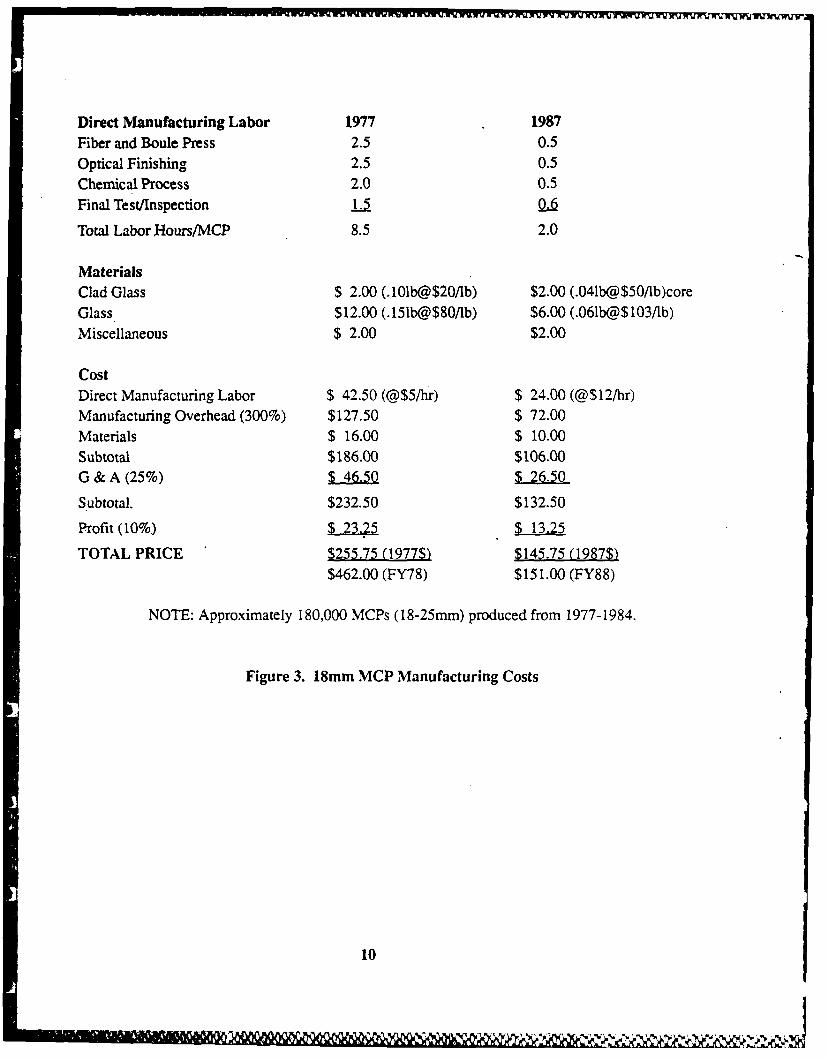
Direct Manufacturing Labor 1977 1987Fiber and Boule Press 2.5 0.5Optical Finishing 2.5 0.5Chemical Process 2.0 0.5Final Test/Inspection 1.5
Total Labor Hours/MCP 8.5 2.0
MaterialsClad Glass $ 2.00 (.101b@$20/Ib) $2.00 (.041b@$50/lb)coreGlass $12.00 (.151b@$80/lb) $6.00 (.061b@$103/lb)Miscellaneous $ 2.00 $2.00
CostDirect Manufacturing Labor $ 42.50 (@$5/hr) $ 24.00 (@$12/hr)Manufacturing Overhead (300%) $127.50 $ 72.00Materials $ 16.00 $ 10.00Subtotal $186.00 $106.00G & A (25%) $ 46.50 $ 26.50
Subtotal. $232.50 $132.50
Profit (10%.) $ 23.25 $ 13.25
TOTAL PRICE $255.75 (1977$) $145.75 (1987$)$462.00 (FY78) $151.00 (FY88)
NOTE: Approximately 180,000 MCPs (18-25mm) produced from 1977-1984.
Figure 3. 18mm MCP Manufacturing Costs
10

"APENDIX A
72N
APPLICATIONS for
MICROCHANNEL PLATES
varian@
A-1
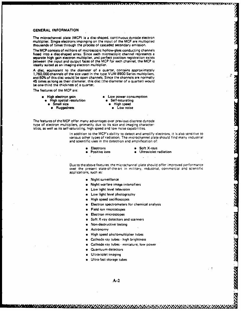
GENERAL INFORMATION
The microchannel plate (MCP) is a disc-shaped, continuous dynode electronmultiplier. Single electrons impinging on the input of the MCP are multipliedthousands of times through the process of cascaded secondary emission.The MCP consists of millions of microscopic hollow-glass conducting channelsfused into a disc-shaped array. Since each microscopic channel represents aseparate high gain electron multiplier, and perfect position registration existsbetween the input and output faces of the MCP for each channel, the MCP isideally suited as an imaging electron multiplier.A disc, equivalent to the diameter of a quarter, contains approximately1,760,000channels of the size used in the type VUW-8900 Series multipliers,and 60% of this disc would be open channels. Since the channels are normally45 times as long as their diameter, this disc (the diameter of a quarter) wouldbe one-third the thickness of a quarter.The features of the MCP are:
High electron gain a Low power consumptione High spatial resolution e Self-saturating
9 Small size 9 High speed* Ruggedness 9 Low noise
The featuresof the MCP offer many advantages over previous discrete dynodetype of electron multipliers, primarily due to its size and imaging character-istics, as well as its self-saturating, high speed and low noise capabilities.
In addition to the MCP's ability to detect and amplify electrons, it is also sensitive tovarious other types of radiation. The microchannel plate should find many industrialand scientific uses in the detection and amplification of:
e Electrons * Soft X-rayse Positive ions e Ultraviolet radiation
Due to the above features, the microchannel plate should offer improved performanceover the present state-of-the-art in military, industrial, commercial and scientificapplications, such as:
"* Night surveillance"* Night warfare image intensifiers"* Low light level television"* Low light level photography"* High speed oscilloscopes"* Electron spectrometers for chemical analysis"* Field ion microscopes
"* Electron microscopes"* Soft X-ray detectors and scanners"* Non-destructive testing"* Astronomy"* High speed photomultiplier tubes
"* Cathode ray tubes - high brightness"* Cathode ray tubes - miniature, low power" Quantuum detectors
"* Ultraviolet imaging"* Ultra-fast storage tubes
A-2 !,VXIL

BACKGROUND
Varian Associates has been in the field of continuous channel electronmultiplier arrays since early 1967, and is the largest supplier of these devicesin the United States, having supplied over 80% of the military requirementsfor microchannel plates for use in night vision devices since 1969. We haveone of the finest Production, Engineering and Development teams availableto develop and produce channel multiplier devices to customer specifications.
Until June 1971, the MCP was classified "Confidential" by the U.S. Depart-ment of Defense, but is now unclassified. Because of its prior classification,the major application of the MCP until recently has been in military secondgeneration direct-view night vision systems, such as:
a Night vision gogglese Crew-served weapon sight e Small starlight scope
Future military systems which offer potential applications are:
"* Tank periscopes"* Night vision aerial periscopes"* Night rescue helicopter missions"* Continuing army direct-view night vision scopes and goggles
Future uses of the MCP in non-military devices are multiform and various, andare discussed in a subsequent section on Applications.
PRINCIPLE OF OPERATION
The glass channels in the MCP, are connected in parallel electrically by metal electrodeson opposite faces of the disc. The MCP, which must operate in a vacuum, is speciallyprocessed to produce secondary electrons from the channel surfaces. When radiationimpinges on the input of the array, -secondary electrons are generated. These secondaryelectrons are accelerated when voltage is applied between the disc faces. Secondaryelectrons passing along the channels, collide with the channel surfaces to dislodgeadditional secondary electrons, thereby producing electron multiplication, or ampli-fication. By varying the voltage across the disc, the gain of the multiplier can be con-trolled. The following illustration shows the principle of operation of an MCP.
PHOTO PHOSPHORCATHOOE MICROCHANNEL SCREENPLATE J
S. LIGHT
- ",,, INOIVIOUAL
SSECONOARY MULTIPLIERS ELECTRONS TUBE
INPUTELECTRON.
CONTACT -- |F;*11 CONTACT
A-3

TYPICAL CHARACTERISTICS
The performance characteristics of a device such as the microchannel plate obviouslydepend on a complex interaction of its several electrical parameters with its physicalparameters. Fortunately, these parameters can be manipulated to obtain certain de-sired performance effects. Prospective MCP users are encouraged to discuss theirparticular requirements in the application of MCP's with Varian's technical staff.
A discussion of MCP characteristics follows:100
Ld 58
BIAS
In an MCP, the channels (or holes) are at a Udc = 42
bias with respect to the parallel input and
output surfaces. Typical values of this biasangle are 50 and 80 with respect to the plate .ksurfaces. The intent of this bias angle is to: 10
"* reduce ion feedback IfX
L/dc 3"* Increase the probability of impact ofthe incoming energy with the channel ,
surfaceIf
I reduce direct light feedback from out- t2 1.0put phosphor screens K
0 ITHICKNESS
The thickness of the MCP is dependent upon xthe channel hole size, and is usually designedfor the particular user application. Typically,the L/dc of the channels is in the range of 0.135 to 55 depending upon the end parameters de =4(i.e. gain and uniformity) desired. For an Lidcof 50, the VUW-8900 series MCP thickness is Gmax = 1000 V gain
approximately 0.023 inch. for 58 L/dc condition
OPEN-AREA-RATIO 0.01" -
The Open-Area-Ratio (OAR) of the MCP is 400 600 buO 1000 1200defined as the ratio of the open area to thetotal area of the MCP. Typically, the OAR of Multiplier Voltage (VM)
MCP's is greater than 50%.
3
A-4
011 11 1 = 11 IIS111111 111 1 1 p .

GAIN The typical electron gain of the MCP is a functionof the multiplier voltage and the input currentdensity into the array. For example, in a VUW-8900Series MCP, below 700 volts the multiplier gain is
- - - - independent of the input current density. Abovethis voltage, the secondary electrons emerging fromnear the end of the channels raises the potential ofthe channel wall until there is a low field regionwhich either maintains, but does not augment, thegain process, or actually acts as an electron sink
I* (commonly referred to as gain saturation). This situ-ori'4 ation is analogous to that in a-conventional photo-
multiplier when the output current from the last104 - -___ dynode exceeds the bleeder current in the resistor
"chain across the dynodes. In a microchannel plate,the output current is limited by the standing current
_- along the walls of each channel, which is commonlyreferred to as the strip current of the multiplier.
Therefore, as the resistance of the multiplier is de-creased, the strip current in the multiplier increases
C and the saturation voltage increases. As a general rule0 of thumb, the gain of the multiplier array is linear
- -3; c"".'olrnnv up to the point where the output current density"from the multiplier begins to exceed 5% of the stripcurrent. A typical value for strip current in presentstate-of-the-art microchannel plates is approxi-mately 1 x 10.6 A/cm 2 of active disc diameter.
The limiting current characteristics of the MCP isnormally seen by referring to the current transfercurves for the device. This self-saturating feature is
102 one of the prominent advantages of the MCP in lowlevel applications.
/E01 - - - aE /
500 G0o 700 a00 900 1000 1100
Multiplier Voltage ,
Typical Characteristics j ,.
L/dc = 42dc = 14.5 g"OAR = 60 % (T t
R = 3 x 10 8 •.2 r -3 W2 '0 ,1 0 164
Input Current Density (A/cm2 )
4
A-5
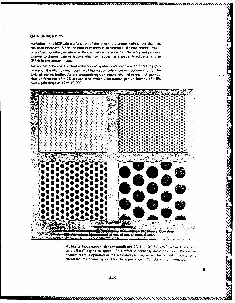
GAIN UNIFORMITY
Variation in the MCP gain asa function of the length-to-diameter ratio of the channelshas been discussed. Since the multiplier array is an assembly of single channel multi-pliers fused together, variations in the channel diameters within the array will producechannel-to-channel gain variations which will appear as a spatial fixed pattern noise(FPN) in the output image.
Varian has achieved a virtual reduction of spatial noise over a wide operating gainregion of the MCP through control of fabrication tolerances and optimization of theL/dC of the multiplier. As the photomicrograph shows, channel-to-channel geomet-rical uniformities of ± 2% are achieved, which yield output gain uniformity of + 5%over a gain range of 10 to 10,000.
- ~ ~ ~. .. . .. *.;. . .--. ;... .- .." ""• .- .. .... ........................ .. . .
*000 0 0 0 0
.... . . .
-.-
t46Wi-pan Am&
At higher input current density conditions ( >1 x 10⁻¹⁰ Acm2 ), a slight "chickenwire effect" begins to appear. This effect is primarily noticeable when the micro-channel plate is operated in the saturated gain region. As the multiplier resistance isdecreased, the operating point for the appearance of "chicken wire" increases.
A-6
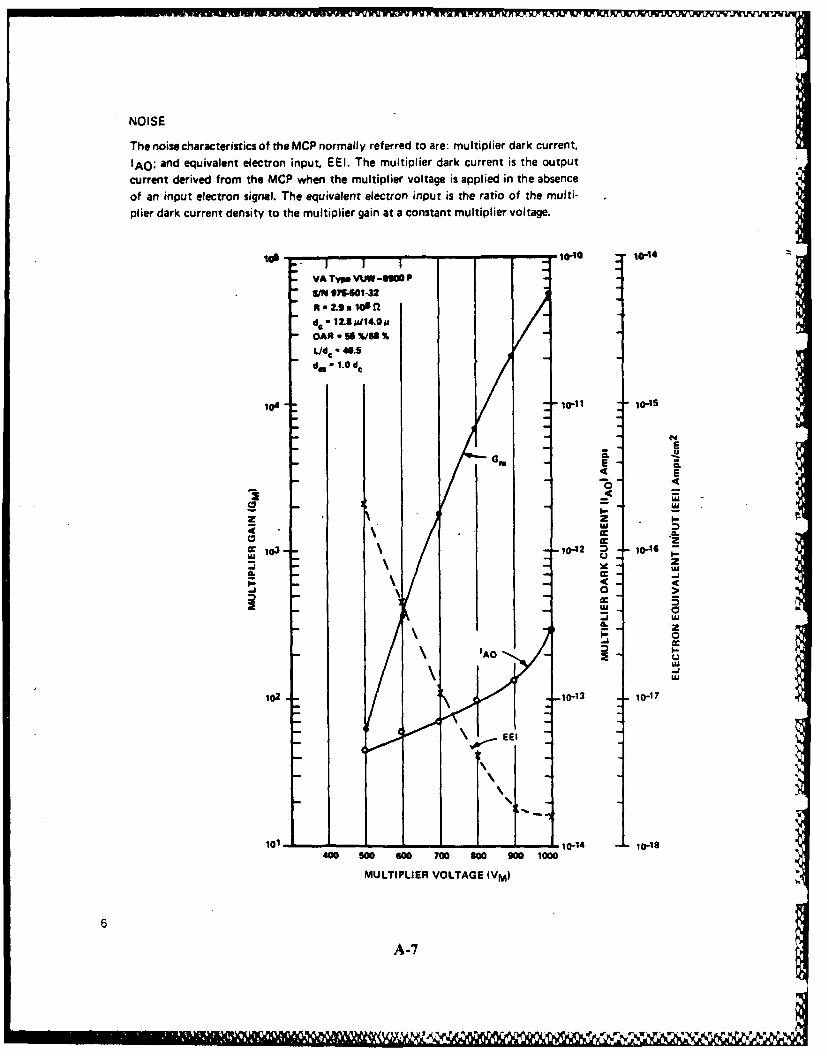
NOISE
The noise characteristics of the MCP normally referred to are: multiplier dark current,
IAO; and equivalent electron input, EEl. The multiplier dark current is the outputcurrent derived from the MCP when the multiplier voltage is applied in the absenceof an input electron signal. The equivalent electron input is the ratio of the multi-plier dark current density to the multiplier gain at a constant multiplier voltage.
I 1" 1 -100•-10
VA Type VUW -IMo PSIN 975-601-32n - 2.93 loa nlde -12.8 W14.0 m
OAR - 55 %M63%L/d 6 ",4.5
do. 1.0 dc
104 - -10-11 10-1S
' "2G C E4-C E
0. *,.2
102 _10-13 101C -
x" 10- &2M l4
z2U
CC-
'AO
wj
1210-13 10*47
MULTIPLIER 700 80o0 0 1000
MULIPLERVOLTAGE fVM)
6
A-7

RESOLUTION Therefore, optimization between end spoiling
The basic limitation to resolution obtainable from depth, center-to-center channel spacing, and gain,microchannel plates (at high input levels), is the must be realized with regards to resolution require-center-to-center channel spacing. Generally, for an ments. Optimum compromise is in the range ofhexagonal close-pack channel structure with center- 1.0 dc to 2.0 dc.to-center channel spacing p, the resolution limit isgiven by 1/2 p. In order to increase the probability that the first
SIMo impact of incident radiation occurs on the innerglass surface, and not on the input electrode, theinput electrode penetration is usually controlled to
>4010.5 dc to 0.8 dc.
.2
Active rea (m-201000-
2 d
- 0 d0 i i I 0 0 10 ____;_ O
0 20 40 00 so to0A
Active Area I(mm)0dcd
E 40C
30-(
20-2~1.0
01 N
Center to Center Channel Spacing IP) (microns) for~ - 1000 dc descondto
fow 10 -escodiio
In many microchannel plate image intensifier appli-F Ications, the phosphor viewing screen is placed in 0.1 /II1close proximity to the output of the microchannel L dc 42 "plate. The resolution attainable is then a functionof the electric field applied across this proximityL
A technique commonly used to increase the reso- to/_Lulo'=" trlton capabilities of te poxmt output ston~o /is termed "end spoiling" of the output electrode. iI.End spoiling refers to the penetration of the output EM~ta• 0 8 dc denelectrode into the channels of the multiplier array linpu,in order to collimate the output electron beam. 00The end spoiling depth (des) is denoted in terms of 4oo 600 Soo 1000 12ochannel diameters (dc). End spoiling affects theovyerall gain of the multiplier. MULTWILIER VOLTAGE (VMI
A-8

OPERATIONAL LIFE
Microchannel plates have been continuously operated up to 7800 hours. The pre-vious processing history of the MCP is an important factor in its life charac-teristics. Extreme cleanliness is required in the handling and processing of MCP's. Thedifferences in the life characteristics of the two MCP's shown can be attributed topreprocessing history.
90
70
so
40
30
Varian Associates; Multiplier Type VUW-8900 H20 ~Conitinuous Oporation: VM 1000 v. & J1 3 x 10-12 A/cm2
10
TIME (Hours)
975-407-05 975-407-06Go7.4 x 103 4.4 x 10³
R 2.6 x10⁸ n 3.1 x10⁸ 0dc14.6 g 14.6 Mu
Lidc 43.5 42.6OAR 58% 58%des 3 dc 3dc
DETECTION EFFICIENCY
The MCP is sensitive to many types of radiation. The detection efficiency is definedas the percentage of input particles or quanta producing det~ctabIe pulses at the mnul*
tiplier output. A chart of the detection efficiency of the MCP to various types ofradiation in various energy ranges is given.
A-9

DETECTION EFFICIENCY
100-
90-
so_
10 to 50 Kew
70
.5 to 4 Kiev>- 60 3 to 10 KevU.1 I
u. 50, 50 to 200 KvU1
w 40-. 0.1 to 0.5 Kev
30
* 30
4 Kie to 100 Key0.5 to 3 Kew I
20-
10 I .1T 300 to 1150k2.1 X to 68
0 toI 150
Positive Ions Electrons Soft X.Ray U.V.
TYPE OF RADIATION
TRANSIT TIME
The electron transit times through the MCP are less than 1 nanosecond with atransit time spread of approximately 0.1 nanosecond. Therefore, the MCP is ideallysuitable for applications where detection of high speed phenomena, events isrequired. A-IO
9,

APPLICATIONS IMAGE TUBE APPLICATIONS
The MCP can be operated as a single plate multiplier, PhtIth~d MCPor in a tandem-dual plate operation.
The single plate mode of operation is used primarily ,e Screen
in the following applications. f "-ELECTROSTATIC FOCUS
e Image intensifiers (various types)' IMAGE INTENSIFIER
I Camera tubes P
e Cathode ray tubes .h
Where detf:tion of quantum events is required, the
tandem arrangement of channel multiplier plates is PROXIMITY FOCUS
used. In this application, two microchannel plates IMAGE INTENSIFIER
are placed in close proximity (approximately 1 mil
separation) with their bias angles opposing (op- MP
posing bias angles is used to reduce ion feedback Potoade
effects). In this configuration, electron gains in ex. Dr. Phosphor Screen
cess of 107 can be achieved. Typical output noise
dark counts which have been routinely achieved in
this configuration are 1.1 to 1.7 counts/sec/cm 2 , Solenoid
over an operating voltage range of 1600 to 2200 ELECTROSTATIC & MAGNETICvolts. FOCUS IMAGE INTENSIFIER
SPACER ELECTROOE
ANOOE MCP MCP ANODE
IPh9olact Scree n) No.1 2 Ph.hor Scree)
INCIDENTINCIDENT RADIATION
RADIATION
21W 1M 2MM
m I2
DC P pS. oc P.s. PSO .S
SINGLE PLATE OPERATION TANDEM-DUAL PLATE OPERATION
A-Il

CRT APPLICATION
Electron-Gun - -
J~ J ! C
-
Deflection System -
(Electrotatic orMagnetic) C
Phosphor Viewing Screen
CAMERA TUBE APPLICATION
ReadoutElectronMCP Beam
Photocathode Target
AVAILABLE TYPES
Microchannel plates are classified in accordance with their channel to channel spacing (pitch).and imaging active area. plate overall diameter, as follows:
Center-to-Center Channel Soacing. Ditch (microns)
Useful IImaging PlateArea Diameter 12 5 15 50m mM l min,
18 .975 VUW 8921 VUWV.8900 -
25 1 287 8922 8911 -
25 1410 - I VUA .8964
40 1 970 -8908 8968
All types except for the 40mm useful imaging area MCP's have solid glass borders from tfleactive area to the plate outside diameter.
The VUW-8920 series MCP's are considered the high resolution tyve. in contrast to themedium resolution VUW-8900 series and low resolution VUW-8940 series.
The primary application of the 8960 series is in spatial quantuum detectors and or amplifiers.
The above information by no means covers the capabilities available. We welcome nouirieswith regards to other variations to the customer specifications.
A-12
mumI

WilIWWFrRGLOSSARY OF TERMS - MICROCHANNEL PLATES
PARAMETER UNITS SYMBOL OEFINITION
input Surface: - -Surface of channel electron multiplier with largest geometrical electrode
pattern. (Noted on VA Type Drawings)
Output Surface: - -Surface of channel electron multiplier with smaller geometrical electrodepattern. (Noted on VA Type Drawings)
Qhvstannl D..e.,,ete: microns dc The diameter of the individual channels (holes) in the microchannel plate.
Channel Pitch: microns P The center-to-center channel spaing.
Sias Angie: degrees a1 Angle formed by the axis of the channel and the normal to the platesurfaces.
End Spoiling: dc des Depth of penetration of the output electrode into the individual channels
Open Area Ratio: %OAR The ratio of open area of the multiplier to the total area of the multiplier.
Dimte:OAR -. 907 ldc) 2
OcDiameer inches D Outside diameter of the Channel Multiplier ArraVUseful Area: mm AA The area of the array which is available for useful imaging.
NOTE This area is highly dependent upon individual uisers final tubemounting assembly design.
Length to Diameter Ratio: - L/dc Ratio of the thickness of the multiplier to the hole diameter of the chnaniels
Electrode Area: cm2 AE Area of the output electrode surface.
fAlluesplier Voltage: volts VM Voltage aoplied between the input and output surfaces of the multiplierPositive polarity on output.
Strip Current: amps IS Current that flows through multiplier when multiplier voltage is applied inthe absence of input electron signal,
Operating Current: amps lop Current that flows through multiplier when multiplier voltage is applied and
input electron signal is applied.
Mluiltiplier Resistance: ohms R Ratio of multiplier voltage to strip current
R =VM (ohms)
Is.
Multiplior Resistivity: . ohms- Product of electrode area and the multiplier resistance. e , the resistance of
cm2
a one sQuare cm. multiplier
p =A- F5 ohms-cm2
)
Multiplier output Current: amps IA Output current derived from multiplier when multiplier voltage and sigrilacurrent is applied.
Multiplier input Current: amps ,ýn Input current signal presented to the input surface of thie muitipi ýer
Multiplier Dark Current- amps ;AO Output current derived from multiplier when multiplier voltage is appitedtand n the absence of an input electron signal
Mifultiplier Dark amos JAO Ratio of the multiplier dark current to electrode areaCurrent Density c_
2 ~O A
Equivalent Electron 3n105 EEl Ratio of the multiplier dark current density to the muit Di~er gan at aInput: c2conrstant multlipier voltage
EEl jAO
Multiplier Gain. - M~ Curnt gai of the muirii.ereRatip of -rut riuitipiier Siutpt cjir--ynt -niuus tiro dark cu~-e-t 7o
CiA . (A - (Ao
I.,
W~hir- The inout and oiutput areas piitvr tie i-Uitiivre Qaut becomres theratio of thecCurren~t densities
G%4 x J - JAO
Fieed Pattern Noise - FPhI Spatiai gain nonun Iprmruty c3used by ýeometrtca, tuanurci po cuanne,,ariationi
Chicken Wire@: - renaqorai rlark SC"uiuiiu ,-lfnCt ý3,,Sed 01 Tioi~~ r-ui ýSnv CP s boo-ated n atirjrto,
12
A-13

A ALW1VVi
varian
.... 1.*
0.0~ * .0000
LIGHT SENSING AND EMITTING DIVISION/611 Hansen Way, Palo Alto, California 94303/Telephone. (415) 493-4000
A-14
DISTRIBUTION FOR REPORT NO. 0064
Center for Night Vision and Electro-OpticsCommander, Sacramento Army Depot
6 AMSEL-RDNV ATTN: SDSSA-MSD-3I AMSEL-RD-NV-D-CS Sacramento, CA 95813-50002 AMSEL-RD-NV-PA/ILS
12 AMSEL-RD-NV-TS Commander, US Army Signal Center
I AMSL-RD-V-ITand Fort Gordon1 AMSEL-RD-NV-TS-SOT I ATTN. ATZH-CDLI AMSEL-RD-NV-V I ATTN: ATZH-DTN
I AMCEO-IE-NVDFort Gordon, GA 30905
Department of the Army Commander, US Army Systems Analysis
AgencyCommander, TRADOC I ATTN: AMXSY-CS
1 ATTN: ATCD-ML I ATTN: AMSTE-EV-RI ATTN: ATCD-TE 1 ATTN: AMSTE-E V-S
Fort Monroe, VA 23551-5000 1 ATTN: AMSTE-TE-T
Headquarters, Department of the ArmyAbrenPoigGudM 210
Program Executive OfficerIntelligence Electronic Warfare
Vint Hill Farm StationWarrenton, VA 22-186-5115
Commander, CECOM1 ATTN: AMSEL-TDDI ATTN: DELSD-LI AMSEL-ME-PSL
Fort Monmouth, NJ 07703-5001
Commander, AMCATTN: AMCSM-NC5001 Eisenhower AvenueAlexandria, VA 22333
Defense Technical Information CenterATTN: DTIC-FDACameron Station, Bldg 5Alexandria, VA 22304-6145
Commander, US Army Materiel ReadinessSupport
I
ActivityATTN: AMXD-EDLexington Bluegrass DepotLexington, KY 04511-5101
!!III~~~ Id 101,111