development of a 10-inch hpd with integrated readout...
TRANSCRIPT

Beaune 2002, C. Joram / CERN
Development of a 10-inch HPD
with Integrated Readout Electronics
A. Braem, E. Chesi, C. Joram, J. Séguinot, P. WeilhammerCERN
M. Giunta , N. Malakhov, A. Menzione, R. Pegna, A. Piccioli, F. Raffaeli INFN Pisa
1. CLUE – an air shower Cherenkov experiment2. The 5-inch Pad HPD3. Development of a 10-inch HPD4. Rb2Te photocathode5. Self triggering readout electronics

Beaune 2002, C. Joram / CERN
CLUE = Cherenkov Light Ultraviolet Experiment
Imaging Air Cerenkov Telescopewith 9 detector units
40 m Single unit" F/1 Parabolic Mirror, 1.8 m Ø" UV Detector in focal plane
e-
quartzgas
+ TMAE
segmented cathode
…………………..Npe ~ ∫ QE·Tquartz · TO2 dE
now futureMWPC 10” HPD
× 20

Beaune 2002, C. Joram / CERN
1 step back: The 5-inch Pad HPD
hν
e-
Si sensor
Focusing electrodes
Indium joint
127 mm
• Bialkali K2CsSb cathode on UV extended borosilicate window (schott 8337)
• 114 mm active diameter• Si sensor, 2048 channels, 1 × 1 mm2
• Integrated readout electronics (IDEAS VA2, VA-prime)
• Nominal operational voltage: 20 kV
• Originally developed for LHCbRICH detectors
• Since January 2000 continued as independent R&D project
• Fountain focusing optics• D ~ 2.4 à segmentation on cathode 2.4 × 2.4 mm2
VA2 chips Ceramic with 2 signallayers
Si detectorWire bonds

Beaune 2002, C. Joram / CERN
QE and uniformity (K2CsSb cathode)
Radial dependence of the quantum efficiency of HPD PC68 for λ=230, 290 and 350 nm.Non-uniformity (±10%) mainly due to reflections from Si and electrodes.
200 300 400 500 600
lambda (nm)
0
4
8
12
16
20
24
28
32
Q.E
. (%
)
HPD PC87(produced Easter Sunday 2001)
trans
pare
ncy
of w
indo
w
“one of the best”
Peak QE in the range 25±3% is routinely reached !
Beaune 2002, C. Joram / CERN
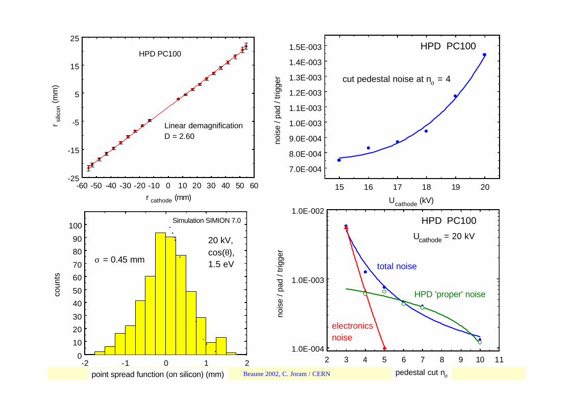
15 16 17 18 19 20
Ucathode (kV)
7.0E-004
8.0E-004
9.0E-004
1.0E-003
1.1E-003
1.2E-003
1.3E-003
1.4E-003
1.5E-003
nois
e / p
ad /
trig
ger cut pedestal noise at nσ = 4
HPD PC100
2 3 4 5 6 7 8 9 10 11
pedestal cut nσ
1.0E-004
1.0E-003
1.0E-002
nois
e / p
ad /
trigg
er
Ucathode = 20 kV
HPD PC100
total noise
electronics noise
HPD 'proper' noise
-2 -1 0 1 2point spread function (on silicon) (mm)
0
10
20
30
40
50
60
70
80
90
100
coun
ts
σ = 0.45 mm
20 kV, cos(θ), 1.5 eV
Simulation SIMION 7.0
-60 -50 -40 -30 -20 -10 0 10 20 30 40 50 60r cathode (mm)
-25
-15
-5
5
15
25
r sili
con (m
m)
Linear demagnificationD = 2.60
HPD PC100

Beaune 2002, C. Joram / CERN
0 2 4 6 8 10 12 14 16 18 20 22Ucathode (kV)
0
5
10
15
20
25
sign
al a
mpl
itude
(A
DC
cha
nnel
s)
E0 = 1.5 keV
HPD PC100
0 10 20 30 40 50 60 70 80 90 100
signal amplitude (ADC channels)
0
20
40
60
80
100
120
140
160
coun
ts
HPD PC100
20 kV VA' chip set (350 ns shaping time)
<signal> = 23.13σ = 2.74
4 σ
cut

Beaune 2002, C. Joram / CERN
LHCb beam test with aerogel radiator (May 2001)
Courtesy of LCHb/RICH group
Use Pad HPDsPC84 / 85 / 86 / 87
See separate poster(Tito Bellunato et al.)

Beaune 2002, C. Joram / CERN
The 10-inch HPD
Characteristics of the final version
• Rb2Te cathode, 4-7 eV, “solar blind”
• Quartz or UV ext. borosilicate window
• Demagnification ca. 4
• Segmentation on cathode level ca. 4 x 4 mm2
• Integrated self triggering electronics
• Envelope originally designed and fabricated for the AQUARICH prototype experiment (T. Ypsilantis et al.)

Beaune 2002, C. Joram / CERN
HPD’s development and production at CERN
1998 – 2001 à HPD 5”• Optimised for RICH
applications (LHCb)
• K2CsSb photocathode
• UV extended window
• 2048 readout pads
• Optimised for Cherenkov based air shower detectors
• UV extended (or quartz) window
• Rb2Te photocathode
2001 - 2003 à HPD 10”

Beaune 2002, C. Joram / CERN
U = -20 / -19.6 / -16. / -13.5 / -7 kV
Electron optical simulations(SIMION 7.0)

Beaune 2002, C. Joram / CERN
D ~ 4
0 5 10 15 20 25 30R silicon (mm)
0
20
40
60
80
100
120
R c
atho
de (
mm
)
-5 -4 -3 -2 -1 0 1 2 3 4 5
xsilicon (mm)
-5
-4
-3
-2
-1
0
1
2
3
4
5
y silic
on (
mm
)
Electron optical simulations (cont’d)
Linear demagnification up to R=120 mm
Electron distribution on silicon for pointsource at xcathode = ycathode = 0
projection
-5 -4 -3 -2 -1 0 1 2 3 4 5point spread function (mm)
0
20
40
60
80
100
120
140
160
RMS = 1.3 mm
Ucathode = -20 kV
<Ekin> = 1.5 eV, cos(θ) distributed emission

Beaune 2002, C. Joram / CERN
The Rb2Te photocathode
200 250 300 350 400 450 500
λ (nm)
0.00001
0.00010
0.00100
0.01000
0.10000
1.00000
10.00000
Q.E
. (%
)
Cs2Te
Rb2Te
Hamamatsu….Rb2Te has similar
characteristics than the well known ‘solar blind’ Cs2Te cathode.
However, very important for our application: the response of Rb2Te above 300 nm is ~10-100 times lower.
Resistivity of cathode is very high: > 1010 O/•Conductive under-coating required to allow for reasonable photocurrents and uniform cathode response.

Beaune 2002, C. Joram / CERN
Indium Tin Oxide (ITO) ïð Chromium as transparent conductive layers
Our standard layer:
• ITO film thickness : 3.2nm• Vacuum evaporated + post oxidation in air at 300ºC for 8 hours
Measured transmission of UV extended glass (Schott 3337) coated with ITO
0
0.2
0.4
0.6
0.8
1
200 300 400 500 600Lambda [nm]
Tra
nsm
issi
on
window
window + ITO
Resistance versus average transmission (200 - 400nm) of ITO and Cr thin films on Quartz
0.40
0.50
0.60
0.70
0.80
0.90
1.0E+03 1.0E+05 1.0E+07 1.0E+09 1.0E+11Resistance [ohm/square]
Tra
nsm
issi
on
Cr 1.9nm Cr 3nmCr 5.5 ITO 1.6nmITO 2.6nm ITO 3.2nmITO 3.9nm ITO 4.8nmITO 5.9nm ITO 6.3nm
Cr
ITO
3.2 nm

Beaune 2002, C. Joram / CERN
The Rb2Te co-evaporation process
Turbo Pump
monochromator(200-800 nm)
Te Rb
• Excellent vacuum after bake-out (160ºC, tube at 300ºC)
p ~ 5•10-9 mbarpH2O ~ 1•10-9 mbar
• Tank + substrate at T ~ 70ºC
• Permanent monitoring of Iphoto, all other essential parameters (p, T, Isource)
• Start with evaporation of Rb only à Iphoto ~ few pA
• Co-evaporate Rb and Te
• Stop when Q.E. (250 nm) reaches maximum

Beaune 2002, C. Joram / CERN
The HPD development plant
• Coat substrates up to φ 10”
• Adapted to UV–VIS PCs, from 200 to 800 nm
• Press mechanism for cold indium encapsulation (2.5 tons)
• Production capacity limited to~ 1.5 HPD / week

Beaune 2002, C. Joram / CERN
200 240 280 320 360 4000
2
4
6
8
10
12
14
16
18
20
QE
(%
)PC99, Rb
0
10
20
30
40
50
60
70
80
90
100
T H
PD
(%
)
λ (nm)
Direct measurement
Extrapolation to quartz window
200 240 280 320 360 400
λ (nm)
0.001
0.010
0.100
1.000
10.000
QE
(%),
extra
pola
ted
to q
uartz
win
dow
HPD PC101
HPD PC99 HPD PC101
Two HPDs produced
Ref. Hamamatsu

Beaune 2002, C. Joram / CERN
Side discovery: Under-layer has strong influence on cathode growth.
0
8
16
24
32
Q.E
. (%
)
PC 92 (ITO, 3nm)
250 350 450 550 650
λ (nm)
PC 87
PC90 (ITO, 3nm)
PC 93
ITO seems not work for K2CsSb cathodes !
200 220 240 260 280 300 320 340 360 380 400
λ (nm)
0
1
2
3
4
5
6
7
Q.E
. (%
)
hemiphere with ITO
hemisphere without ITO
no correction for transparency of borosilicate window
Photocathode PC96
º»Half of HPD window coated with ITO (3 nm)
ITO noITO
2 bialkali photocathodes with ITO2 bialkali photocathode without ITO

Beaune 2002, C. Joram / CERN
Set-up for holding and heating the 10” envelope during evaporation
All components machined in Pisa, most of them now finished.
Heater consisting of 3 spiral heating
elements.
2
3
1
envelope

Beaune 2002, C. Joram / CERN
preamp slowshaper
S&H
silicon diode
hold
Vthr
trigger out
silicon diode Vthr
rea
do
ut
log
ic (
se
ria
l o
r s
pa
rse
)
gainfastshaper discr. monostable
128 channels
differential analog out
200 ns
3 µs
Electronics: IDEAS VaTagp3 - a self triggering analogue chip
Sparse readout scheme allows readout rates > 100 kHz.
Existing chip:
= 3 µs
= 150 ns
noise ~ 350 e- (ENC)
slowpeakτfastpeakτ
Faster chip under design
= 1 µs,
= 35 ns
slowpeakτfastpeakτ

Beaune 2002, C. Joram / CERN
Summary and outlook
The 5-inch Pad HPD works up to specifications. Development practically finished.
The ingredients for the fabrication of a 10-inch solar-blind HPD are being developed
• Co-evaporation process è Excellent Rb2Te (ITO) photocathodes
• Two 5” HPD with Rb2Te cathodes (borosilicate window) produced and characterized
• Electron-optics of 10” tube studied
• Most of the mechanical components for the evaporation plant available
Time plan
• Still in 2002: First 10” HPD with bialkali cathode on glass window, VA-prime electronics
• Summer 2003: First 10” HPD with Rb2Te cathode on quartz window, VaTagp electronics
In our spare time we dream of another nice gadget…

Beaune 2002, C. Joram / CERN
Development of a proximity focused HPD
• Optimized for medical applications
• K2CsSb photocathode
• Flat Sapphire window
• Ceramic rectangular body
• Very high active area fraction