development of a mems piezoelectric microphone...
TRANSCRIPT

DEVELOPMENT OF A MEMS PIEZOELECTRIC MICROPHONE FORAEROACOUSTIC APPLICATIONS
By
MATTHEW D. WILLIAMS
A DISSERTATION PRESENTED TO THE GRADUATE SCHOOLOF THE UNIVERSITY OF FLORIDA IN PARTIAL FULFILLMENT
OF THE REQUIREMENTS FOR THE DEGREE OFDOCTOR OF PHILOSOPHY
UNIVERSITY OF FLORIDA
2011

c© 2011 Matthew D. Williams
2

To my wife, Laura, who came with me to Gainesvillefor four years but stuck with me for six
3

ACKNOWLEDGMENTS
The Interdisciplinary Microsystems Group (IMG) at University of Florida has been
an outstanding place to earn two graduate degrees, and there are many people to thank.
My advisor, Mark Sheplak, deserves tremendous praise for the incredible research group
he put together and now maintains together with David Arnold, Lou Cattafesta, Toshi
Nishida, Hugh Fan, Huikaie Xie and YK Yoon. Over the last six years, Mark has pushed
me well beyond any imagined limitations I had when I arrived, and he has done it with a
mix of bluster, compassion, acumen, and generosity that is unique only to him. I will owe
Mark immensely for any future success that I enjoy. For a young father like myself, he has
also been a terrific role model.
I have benefited significantly from my contact with the other IMG professors as well,
most notably David Arnold and Lou Cattafesta, who are at once tremendous researchers,
teachers, and men. They both served as members of my committee and it was a pleasure
working with them in many different capacities. David Arnold taught me, whether he
knows it or not, about vision; I admire his unique ability to cut through the weeds. I
aspire to Lou Cattafesta’s level of precision in all that I do.
I have enjoyed many fruitful conversations with my other committee members,
Nam-Ho Kim and Bhavani Sankar, as well. Both have always been extremely helpful
and cordial, and I thank them wholeheartedly for all of their support. I also owe David
Norton a debt of thanks for serving on my committee and for granting, as associate dean,
additional flexibility in my funding situation for my final semester.
I entered graduate school with a National Science Foundation Graduate Fellowship
for which I am exceedingly grateful, not just for the funding it supplied but for the
doors that it opened. Boeing Corporation was the sponsor for my dissertation work; I
owe them for the funding they provided and for the privilege of working on a problem
of such importance to them. Jim Underbrink of Boeing always kept a watchful eye on
my progress, and it was our close contact late in the project that really solidified my
4

understanding of the big picture. I benefited immensely from working with him and
cannot thank Jim enough for being so giving of his time and so willing to teach. His
commitment to improve the technology of aeroacoustic measurements is inspiring.
My colleagues within IMG deserve high praise. Ben Griffin has been a mentor to me
since the moment I stepped on the University of Florida campus. I can only hope that
I have contributed a fraction as much to his development as he has to mine. My other
senior colleagues who have since gone on to industry, Vijay Chandrasekharan and Brian
Homeijer, were always tremendously supportive as well. Finally, Jess Meloy is easily the
most simultaneously helpful and knowledgeable person I have ever known; I offer my
sincerest apologies to her for so regularly asking for her circuit expertise.
A bond is formed between graduate students who work on their proposals or
dissertations at the same time, and so it is with fond memories that I will look back
on my time in the trenches with Alex Phipps in the summer of 2008 and Jeremy Sells and
Drew Wetzel in the spring of 2011. I will not soon forget our mutual support (or all the
work).
The combined social and intellectual aspect of IMG cannot be ignored, and so it is in
that spirit that I thank Brandon Bertolucci, Chris Bahr, Dylan Alexander, David Mills,
Erin Patrick, Nik Zawodny, Jessica Sockwell, Miguel Palaviccini, Matias Oyarzun, and
honorary IMGer Richard Parker. Whether at 80’s night, a football tailgate, happy hour,
or a frisbee game, I have been privileged to share their company.
I have worked with many outstanding undergradraduates on this project who deserve
recognition: Tiffany Reagan, Anup Parikh, Adam Ecker, Kaleb Erwin, and Kyle Hughes.
In particular, it is Tiffany Reagan’s relentlessness that has most directly contributed to
the success of this project. Her fingerprints are all over this dissertation.
Thanks are due to David Martin, Osvaldo Buccafusca, and Atul Goel at Avago
Technologies for always working with me on the piezoelectric microphone project in good
5

faith and with expectations for its success. They deserve much credit for the results that
were achieved.
Customer service continues to decline in today’s world, but the people at Bruel and
Kjær, Polytec, and TMR Engineering have not heard. Jim Wyatt and Joe Chou always
came through my answers to my microphone questions when their competitors did not;
Arend von der Lieth and John Foley worked tirelessly to ensure IMG’s laser vibrometer
system stayed running at least until I graduated; and Ken Reed always turned up with
high-quality mechanical parts in record time.
Thanks are due to my undergraduate advisor, Paul Joseph, for turning me on to
research in the first place. In addition, my parents David and Anna made all that I have
accomplished possible. Long before Mark Sheplak was preaching the wisdom of setting his
students up for success and getting out of the way, my parents were doing just that with
their son.
The latter parts of graduate school can be hard on a family, but my wife Laura was a
rock. Words cannot thank her enough for the sacrifices she made to make this dissertation
possible. I did it all for her and our daughter, Callahan.
6

TABLE OF CONTENTS
page
ACKNOWLEDGMENTS . . . . . . . . . . . . . . . . . . . . . . . . . . . . . . . . . 4
LIST OF TABLES . . . . . . . . . . . . . . . . . . . . . . . . . . . . . . . . . . . . . 11
LIST OF FIGURES . . . . . . . . . . . . . . . . . . . . . . . . . . . . . . . . . . . . 13
ABSTRACT . . . . . . . . . . . . . . . . . . . . . . . . . . . . . . . . . . . . . . . . 18
CHAPTER
1 INTRODUCTION . . . . . . . . . . . . . . . . . . . . . . . . . . . . . . . . . . 20
1.1 Motivation . . . . . . . . . . . . . . . . . . . . . . . . . . . . . . . . . . . . 201.2 Research Objectives . . . . . . . . . . . . . . . . . . . . . . . . . . . . . . . 251.3 Dissertation Overview . . . . . . . . . . . . . . . . . . . . . . . . . . . . . 27
2 MICROPHONE FUNDAMENTALS . . . . . . . . . . . . . . . . . . . . . . . . 29
2.1 Sound and Pseudo Sound . . . . . . . . . . . . . . . . . . . . . . . . . . . 292.2 The Realities of Microphone Design . . . . . . . . . . . . . . . . . . . . . . 312.3 Microphone Performance Metrics . . . . . . . . . . . . . . . . . . . . . . . 36
2.3.1 Frequency Response and Sensitivity . . . . . . . . . . . . . . . . . . 372.3.2 Noise Floor and Minimum Detectable Pressure . . . . . . . . . . . . 382.3.3 Linearity and Maximum Pressure . . . . . . . . . . . . . . . . . . . 422.3.4 Dynamic Range . . . . . . . . . . . . . . . . . . . . . . . . . . . . . 442.3.5 Summary of Microphone Performance Metrics . . . . . . . . . . . . 44
2.4 Summary . . . . . . . . . . . . . . . . . . . . . . . . . . . . . . . . . . . . 45
3 PRIOR ART . . . . . . . . . . . . . . . . . . . . . . . . . . . . . . . . . . . . . 46
3.1 Review of MEMS Piezoelectric and Aeroacoustic Microphones . . . . . . . 463.2 Summary . . . . . . . . . . . . . . . . . . . . . . . . . . . . . . . . . . . . 58
4 MEMS PIEZOELECTRIC MICROPHONE . . . . . . . . . . . . . . . . . . . . 62
4.1 Piezoelectricity . . . . . . . . . . . . . . . . . . . . . . . . . . . . . . . . . 624.2 Design for Fabrication . . . . . . . . . . . . . . . . . . . . . . . . . . . . . 664.3 Summary . . . . . . . . . . . . . . . . . . . . . . . . . . . . . . . . . . . . 70
5 MODELING . . . . . . . . . . . . . . . . . . . . . . . . . . . . . . . . . . . . . 71
5.1 Lumped Element Modeling Overview . . . . . . . . . . . . . . . . . . . . . 715.2 Lumped Element Model of a Piezoelectric Microphone . . . . . . . . . . . 73
5.2.1 Elements . . . . . . . . . . . . . . . . . . . . . . . . . . . . . . . . . 765.2.1.1 Transduction . . . . . . . . . . . . . . . . . . . . . . . . . 765.2.1.2 Structural elements . . . . . . . . . . . . . . . . . . . . . . 78
7

5.2.1.3 Acoustic elements . . . . . . . . . . . . . . . . . . . . . . . 805.2.1.4 Electrical elements . . . . . . . . . . . . . . . . . . . . . . 83
5.2.2 Diaphragm Mechanical Model . . . . . . . . . . . . . . . . . . . . . 835.2.3 Frequency Response . . . . . . . . . . . . . . . . . . . . . . . . . . . 88
5.2.3.1 Sensor . . . . . . . . . . . . . . . . . . . . . . . . . . . . . 905.2.3.2 Actuator . . . . . . . . . . . . . . . . . . . . . . . . . . . . 92
5.2.4 Electrical impedance . . . . . . . . . . . . . . . . . . . . . . . . . . 935.2.5 Validation . . . . . . . . . . . . . . . . . . . . . . . . . . . . . . . . 94
5.2.5.1 Diaphragm model validation . . . . . . . . . . . . . . . . . 955.2.5.2 Lumped element model validation . . . . . . . . . . . . . . 97
5.3 Interface Circuitry . . . . . . . . . . . . . . . . . . . . . . . . . . . . . . . 985.3.1 Voltage Amplifier . . . . . . . . . . . . . . . . . . . . . . . . . . . . 995.3.2 Charge Amplifier . . . . . . . . . . . . . . . . . . . . . . . . . . . . 1025.3.3 Noise Models . . . . . . . . . . . . . . . . . . . . . . . . . . . . . . 104
5.3.3.1 Noise model with voltage amplifier . . . . . . . . . . . . . 1055.3.3.2 Noise model with charge amplifier . . . . . . . . . . . . . . 108
5.3.4 Selection . . . . . . . . . . . . . . . . . . . . . . . . . . . . . . . . . 1105.4 Summary . . . . . . . . . . . . . . . . . . . . . . . . . . . . . . . . . . . . 112
6 OPTIMIZATION . . . . . . . . . . . . . . . . . . . . . . . . . . . . . . . . . . . 113
6.1 Design Overview . . . . . . . . . . . . . . . . . . . . . . . . . . . . . . . . 1136.1.1 Design Variables . . . . . . . . . . . . . . . . . . . . . . . . . . . . . 1136.1.2 Objective . . . . . . . . . . . . . . . . . . . . . . . . . . . . . . . . . 115
6.2 Formulation . . . . . . . . . . . . . . . . . . . . . . . . . . . . . . . . . . . 1176.3 Approach . . . . . . . . . . . . . . . . . . . . . . . . . . . . . . . . . . . . 1196.4 Results and Discussion . . . . . . . . . . . . . . . . . . . . . . . . . . . . . 1216.5 Summary . . . . . . . . . . . . . . . . . . . . . . . . . . . . . . . . . . . . 126
7 REALIZATION AND PACKAGING . . . . . . . . . . . . . . . . . . . . . . . . 128
7.1 Realization . . . . . . . . . . . . . . . . . . . . . . . . . . . . . . . . . . . 1287.1.1 Geometry . . . . . . . . . . . . . . . . . . . . . . . . . . . . . . . . 1287.1.2 Fabrication Results . . . . . . . . . . . . . . . . . . . . . . . . . . . 128
7.2 Dicing . . . . . . . . . . . . . . . . . . . . . . . . . . . . . . . . . . . . . . 1307.2.1 Dicing Process . . . . . . . . . . . . . . . . . . . . . . . . . . . . . . 1317.2.2 Dicing Results . . . . . . . . . . . . . . . . . . . . . . . . . . . . . . 134
7.3 Packaging . . . . . . . . . . . . . . . . . . . . . . . . . . . . . . . . . . . . 1347.4 Summary . . . . . . . . . . . . . . . . . . . . . . . . . . . . . . . . . . . . 140
8 EXPERIMENTAL CHARACTERIZATION . . . . . . . . . . . . . . . . . . . . 141
8.1 Experimental Setup . . . . . . . . . . . . . . . . . . . . . . . . . . . . . . . 1418.1.1 Die Selection Setup . . . . . . . . . . . . . . . . . . . . . . . . . . . 1418.1.2 Diaphragm Topography Measurement Setup . . . . . . . . . . . . . 1448.1.3 Acoustic Characterization Setup . . . . . . . . . . . . . . . . . . . . 145
8.1.3.1 Frequency response measurement setup . . . . . . . . . . . 145
8

8.1.3.2 Linearity measurement setup . . . . . . . . . . . . . . . . 1508.1.4 Electrical Characterization Setup . . . . . . . . . . . . . . . . . . . 153
8.1.4.1 Noise floor measurement setup . . . . . . . . . . . . . . . 1548.1.4.2 Impedance measurement setup . . . . . . . . . . . . . . . 1568.1.4.3 Parasitic capacitance extraction setup . . . . . . . . . . . 158
8.1.5 Electroacoustic Parameter Extraction . . . . . . . . . . . . . . . . . 1598.1.5.1 Compliance and mass measurement setup . . . . . . . . . 1608.1.5.2 Frequency response measurement setup . . . . . . . . . . . 1658.1.5.3 Effective piezoelectric coefficient measurement setup . . . . 167
8.2 Experimental Results . . . . . . . . . . . . . . . . . . . . . . . . . . . . . . 1688.2.1 Die Selection . . . . . . . . . . . . . . . . . . . . . . . . . . . . . . . 1688.2.2 Diaphragm Topography . . . . . . . . . . . . . . . . . . . . . . . . . 1738.2.3 Acoustic Characterization . . . . . . . . . . . . . . . . . . . . . . . 175
8.2.3.1 Frequency response . . . . . . . . . . . . . . . . . . . . . . 1758.2.3.2 Linearity . . . . . . . . . . . . . . . . . . . . . . . . . . . . 176
8.2.4 Electrical Characterization . . . . . . . . . . . . . . . . . . . . . . . 1808.2.4.1 Noise floor . . . . . . . . . . . . . . . . . . . . . . . . . . . 1808.2.4.2 Impedance . . . . . . . . . . . . . . . . . . . . . . . . . . . 1838.2.4.3 Parasitic capacitance extraction . . . . . . . . . . . . . . . 184
8.2.5 Electroacoustic Parameter Extraction . . . . . . . . . . . . . . . . . 1878.3 Summary . . . . . . . . . . . . . . . . . . . . . . . . . . . . . . . . . . . . 195
9 CONCLUSION . . . . . . . . . . . . . . . . . . . . . . . . . . . . . . . . . . . . 196
9.1 Recommendations for Future Piezoelectric Microphones . . . . . . . . . . . 1989.2 Recommendations for Future Work . . . . . . . . . . . . . . . . . . . . . . 202
APPENDIX
A DIAPHRAGM MECHANICAL MODEL . . . . . . . . . . . . . . . . . . . . . . 204
A.1 Strain-Displacement Relations . . . . . . . . . . . . . . . . . . . . . . . . . 205A.2 Kirchhoff Hypothesis . . . . . . . . . . . . . . . . . . . . . . . . . . . . . . 207A.3 Equations of Motion . . . . . . . . . . . . . . . . . . . . . . . . . . . . . . 208A.4 Constitutive Equation . . . . . . . . . . . . . . . . . . . . . . . . . . . . . 214A.5 Displacement Differential Equations of Motion . . . . . . . . . . . . . . . . 217A.6 Equations of Equilibrium . . . . . . . . . . . . . . . . . . . . . . . . . . . . 219
A.6.1 Nonlinear . . . . . . . . . . . . . . . . . . . . . . . . . . . . . . . . 219A.6.2 Linear . . . . . . . . . . . . . . . . . . . . . . . . . . . . . . . . . . 221
A.7 Problem Solutions . . . . . . . . . . . . . . . . . . . . . . . . . . . . . . . 222A.7.1 Linear . . . . . . . . . . . . . . . . . . . . . . . . . . . . . . . . . . 223
A.7.1.1 General solutions . . . . . . . . . . . . . . . . . . . . . . . 223A.7.1.2 Particular solutions . . . . . . . . . . . . . . . . . . . . . . 224A.7.1.3 Inner region: tension (x(1) > 0) . . . . . . . . . . . . . . . 226A.7.1.4 Inner region: x(1) = 0 . . . . . . . . . . . . . . . . . . . . . 226A.7.1.5 Inner region: compression (x(1) < 0) . . . . . . . . . . . . 227
9

A.7.1.6 Outer region: tension (x(2) > 0) . . . . . . . . . . . . . . . 228A.7.1.7 Outer region: x(2) = 0 . . . . . . . . . . . . . . . . . . . . 229A.7.1.8 Outer region: compression (x(2) = 0) . . . . . . . . . . . . 230
A.7.2 Nonlinear . . . . . . . . . . . . . . . . . . . . . . . . . . . . . . . . 231A.8 Closing . . . . . . . . . . . . . . . . . . . . . . . . . . . . . . . . . . . . . . 234
B BOUNDARY CONDITION INVESTIGATION . . . . . . . . . . . . . . . . . . 235
C UNCERTAINTY ANALYSIS . . . . . . . . . . . . . . . . . . . . . . . . . . . . 237
C.1 Approach . . . . . . . . . . . . . . . . . . . . . . . . . . . . . . . . . . . . 237C.2 Frequency Response Function . . . . . . . . . . . . . . . . . . . . . . . . . 238C.3 Noise Floor . . . . . . . . . . . . . . . . . . . . . . . . . . . . . . . . . . . 238
C.3.1 Spectra . . . . . . . . . . . . . . . . . . . . . . . . . . . . . . . . . . 239C.3.2 Narrow Band . . . . . . . . . . . . . . . . . . . . . . . . . . . . . . 240C.3.3 Integrated . . . . . . . . . . . . . . . . . . . . . . . . . . . . . . . . 240
C.4 Impedance . . . . . . . . . . . . . . . . . . . . . . . . . . . . . . . . . . . . 240C.5 Parasitic Capacitance Extraction . . . . . . . . . . . . . . . . . . . . . . . 240C.6 Parameter Extraction . . . . . . . . . . . . . . . . . . . . . . . . . . . . . . 241
D MATERIAL PROPERTIES . . . . . . . . . . . . . . . . . . . . . . . . . . . . . 242
REFERENCES . . . . . . . . . . . . . . . . . . . . . . . . . . . . . . . . . . . . . . . 243
BIOGRAPHICAL SKETCH . . . . . . . . . . . . . . . . . . . . . . . . . . . . . . . . 260
10

LIST OF TABLES
Table page
1-1 Fuselage array application requirements. . . . . . . . . . . . . . . . . . . . . . . 27
2-1 Performance characteristics of common aeroacoustic microphones. . . . . . . . . 45
3-1 Summary of MEMS microphones. . . . . . . . . . . . . . . . . . . . . . . . . . . 59
4-1 Typical properties of piezoelectric materials in MEMS. . . . . . . . . . . . . . . 66
5-1 Geometric dimensions of an example device. . . . . . . . . . . . . . . . . . . . . 95
5-2 Comparison of voltage and charge amplifier topologies . . . . . . . . . . . . . . 110
6-1 Microphone dimensions fixed by the fabrication process. . . . . . . . . . . . . . 114
6-2 Design variable bounds. . . . . . . . . . . . . . . . . . . . . . . . . . . . . . . . 118
6-3 Constant values used in the optimization. . . . . . . . . . . . . . . . . . . . . . 121
6-4 Target thin-film residual stresses. . . . . . . . . . . . . . . . . . . . . . . . . . . 121
6-5 Optimal layer thicknesses. . . . . . . . . . . . . . . . . . . . . . . . . . . . . . . 124
6-6 Optimization results. . . . . . . . . . . . . . . . . . . . . . . . . . . . . . . . . . 124
7-1 Design dimensions. . . . . . . . . . . . . . . . . . . . . . . . . . . . . . . . . . 129
7-2 Film properties. . . . . . . . . . . . . . . . . . . . . . . . . . . . . . . . . . . . . 129
7-3 Tape and substrate thicknesses. . . . . . . . . . . . . . . . . . . . . . . . . . . . 132
7-4 Dicer settings. . . . . . . . . . . . . . . . . . . . . . . . . . . . . . . . . . . . . . 133
7-5 Epoxy dispenser settings. . . . . . . . . . . . . . . . . . . . . . . . . . . . . . . 137
7-6 Wire bond settings. . . . . . . . . . . . . . . . . . . . . . . . . . . . . . . . . . . 137
8-1 Die selection laser vibrometer settings. . . . . . . . . . . . . . . . . . . . . . . . 143
8-2 Scanning white light interferometer software settings. . . . . . . . . . . . . . . . 145
8-3 Settings for microphone frequency response measurements in PULSE. . . . . . . 148
8-4 Frequency response measurement settings used at Boeing. . . . . . . . . . . . . 151
8-5 Total harmonic distortion measurement settings used at Boeing. . . . . . . . . . 153
8-6 Noise floor measurement settings. . . . . . . . . . . . . . . . . . . . . . . . . . . 155
8-7 Impedance measurement settings. . . . . . . . . . . . . . . . . . . . . . . . . . . 157
11

8-8 Pressure coupler measurement settings. . . . . . . . . . . . . . . . . . . . . . . . 163
8-9 Settings for sensitivity measurement of pressure coupler microphones. . . . . . . 166
8-10 Wafer statistics. . . . . . . . . . . . . . . . . . . . . . . . . . . . . . . . . . . . . 172
8-11 Pre- and post-packaging LV measurements. . . . . . . . . . . . . . . . . . . . . . 172
8-12 Microphone frequency response characteristics at 1 kHz in air. . . . . . . . . . . 176
8-13 THD measurements performed at Boeing Corporation. . . . . . . . . . . . . . . 180
8-14 Minimum detectable pressure metrics. . . . . . . . . . . . . . . . . . . . . . . . 183
8-15 Extracted electrical parameters. . . . . . . . . . . . . . . . . . . . . . . . . . . . 185
8-16 Open-circuit sensitivity estimates. . . . . . . . . . . . . . . . . . . . . . . . . . . 187
8-17 Extracted mechanoacoustic parameters. . . . . . . . . . . . . . . . . . . . . . . 191
8-18 Extracted electroacoustic parameters. . . . . . . . . . . . . . . . . . . . . . . . . 193
9-1 Realized MEMS piezoelectric microphone performance. . . . . . . . . . . . . . . 197
9-2 Performance characteristics of MEMS piezoelectric microphone 138-1-J3-F. . . . 199
C-1 Parasitic capacitance extraction uncertainties. . . . . . . . . . . . . . . . . . . . 241
D-1 Properties of microphone diaphragm materials. . . . . . . . . . . . . . . . . . . 242
D-2 Properties of gases. . . . . . . . . . . . . . . . . . . . . . . . . . . . . . . . . . . 242
12

LIST OF FIGURES
Figure page
1-1 Boeing 777 fuselage instrumented with an array of microphones. . . . . . . . . . 22
1-2 Aeroacoustic phased arrays deployed as part of the QTD2 program. . . . . . . . 23
2-1 Force-displacement characteristics for a perfect spring. . . . . . . . . . . . . . . 32
2-2 Frequency response of a second-order system. . . . . . . . . . . . . . . . . . . . 33
2-3 Constitutive behavior for a Duffing spring. . . . . . . . . . . . . . . . . . . . . 35
2-4 Various cavity configurations. . . . . . . . . . . . . . . . . . . . . . . . . . . . . 35
2-5 Typical aeroacoustic microphone frequency response. . . . . . . . . . . . . . . . 38
2-6 Noise model for a resistor. . . . . . . . . . . . . . . . . . . . . . . . . . . . . . 40
2-7 Noise model for a resistor in parallel with a capacitor. . . . . . . . . . . . . . . 40
2-8 Low-pass filtering of thermal noise. . . . . . . . . . . . . . . . . . . . . . . . . . 41
2-9 Voltage noise spectrum for an LTC6240 amplifier. . . . . . . . . . . . . . . . . . 41
2-10 Ideal and actual response of a microphone. . . . . . . . . . . . . . . . . . . . . 43
2-11 Operational space of an aeroacoustic microphone. . . . . . . . . . . . . . . . . 45
3-1 Piezoelectric (ZnO) microphone with integrated buffer amplifier. . . . . . . . . . 47
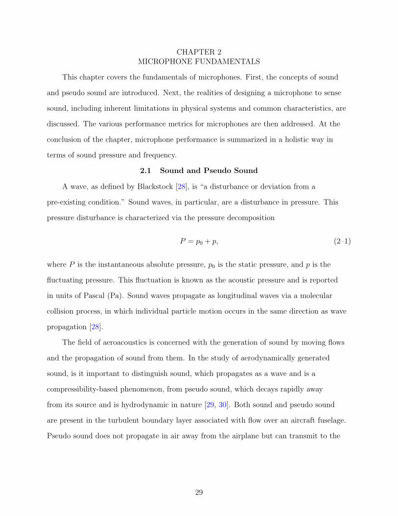
3-2 Piezoelectric (ZnO) microphone utilizing multiple concentric electrodes. . . . . . 48
3-3 Piezoelectric microphone utilizing aromatic polyurea. . . . . . . . . . . . . . . . 48
3-4 Piezoelectric (ZnO) microphone with cantilever sensing element. . . . . . . . . . 49
3-5 Cross section of the first aeroacoustic MEMS microphone. . . . . . . . . . . . . 50
3-6 Piezoresistive MEMS microphone for aeroacoustic measurements. . . . . . . . . 51
3-7 Second-generation aeroacoustic MEMS microphone. . . . . . . . . . . . . . . . . 52
3-8 A dual-backplate capacitive MEMS microphone. . . . . . . . . . . . . . . . . . . 53
3-9 Early PZT-based piezoelectric microphone. . . . . . . . . . . . . . . . . . . . . . 53
3-10 Piezoelectric (ZnO) microphone with two concentric electrodes. . . . . . . . . . 54
3-11 Measurement-grade MEMS condenser microphone developed at Bruel and Kjær. 55
3-12 Piezoelectric (PZT) microphone for aeroacoustic applications. . . . . . . . . . . 56
13

3-13 Top-view of microphone structures from Fazzio et al. (2007). . . . . . . . . . . . 57
3-14 Cross section of a second-generation AlN double-cantilever microphone. . . . . . 58
4-1 Venn diagram for piezoelectric, pyroelectric, and ferroelectric materials. . . . . 63
4-2 FBAR-variant process film stack. . . . . . . . . . . . . . . . . . . . . . . . . . . 67
4-3 Potential circular diaphragm piezoelectric/metal film stack configurations. . . . 69
4-4 Outline of fabrication steps. . . . . . . . . . . . . . . . . . . . . . . . . . . . . . 70
5-1 Illustration of the electrical-mechanical analogy. . . . . . . . . . . . . . . . . . . 73
5-2 Piezoelectric microphone structure. . . . . . . . . . . . . . . . . . . . . . . . . 74
5-3 Piezoelectric microphone lumped element model. . . . . . . . . . . . . . . . . . 75
5-4 Two-port piezoelectric transduction element. . . . . . . . . . . . . . . . . . . . 77
5-5 Laminated composite plate representation of the thin-film diaphragm. . . . . . . 84
5-6 Deflection of a radially non-uniform composite plate with residual stress. . . . . 88
5-7 Boundary conditions applied to a radially non-uniform piezoelectric composite. . 89
5-8 Lumped element model with collected impedances. . . . . . . . . . . . . . . . . 90
5-9 Impedance ratios appearing in the open circuit frequency response expression. . 91
5-10 Comparison of open-circuit sensitivity expressions. . . . . . . . . . . . . . . . . 92
5-11 Lumped element model of the piezoelectric microphone as an actuator. . . . . . 93
5-12 Finite element model for validation exercise. . . . . . . . . . . . . . . . . . . . . 96
5-13 Analytical and FEA predictions of winc(0) (pressure loading case). . . . . . . . 96
5-14 Relative error between analytical and FEA predictions of winc(0). . . . . . . . . 97
5-15 Analytical and FEA predictions of winc(0) (voltage loading case). . . . . . . . . 97
5-16 Lumped element model and FEA predictions of frequency response function. . 98
5-17 Non-ideal operational amplifier model. . . . . . . . . . . . . . . . . . . . . . . . 100
5-18 Lumped element model with voltage amplifier. . . . . . . . . . . . . . . . . . . . 100
5-19 Non-ideal charge amplifier model. . . . . . . . . . . . . . . . . . . . . . . . . . . 102
5-20 Lumped element model with charge amplifier. . . . . . . . . . . . . . . . . . . 103
5-21 Noise model for the microphone with voltage amplifier circuitry. . . . . . . . . 105
14

5-22 Output-referred noise floor for the microphone with a voltage amplifier. . . . . 107
5-23 Noise model for the microphone with charge amplifier circuitry. . . . . . . . . . 108
5-24 Output-referred noise floor for the microphone with charge amplifier. . . . . . . 109
6-1 Cross-section of the piezoelectric microphone with notable dimensions. . . . . . 114
6-2 Pareto front example. . . . . . . . . . . . . . . . . . . . . . . . . . . . . . . . . . 117
6-3 Optimization approach. . . . . . . . . . . . . . . . . . . . . . . . . . . . . . . . 120
6-4 Pareto front associated with minimization of MDP and maximization of PMAX. 122
6-5 Normalized design variable values for each optimization. . . . . . . . . . . . . . 123
6-6 Sensitivity of MDP to ±10 % perturbations in the design variables. . . . . . . . 125
6-7 Sensitivity of PMAX to ±10 % perturbations in the design variables. . . . . . . 126
6-8 Sensitivity of MDP to in-plane stress variations. . . . . . . . . . . . . . . . . . . 126
7-1 Wafer of piezoelectric microphones fabricated at Avago Technologies. . . . . . . 130
7-2 Dicing blade and sample orientation. . . . . . . . . . . . . . . . . . . . . . . . . 131
7-3 Dicing process for MEMS piezoelectric microphone die. . . . . . . . . . . . . . . 133
7-4 Micrographs of microphone die (designs A-G). . . . . . . . . . . . . . . . . . . . 135
7-5 Exploded view of the laboratory test package. . . . . . . . . . . . . . . . . . . 136
7-6 Microphone endcap. . . . . . . . . . . . . . . . . . . . . . . . . . . . . . . . . . 137
7-7 Closeup photograph of a packaged MEMS piezoelectric microphone. . . . . . . 138
7-8 Voltage amplifier circuitry included in the microphone package. . . . . . . . . . 139
7-9 Voltage amplifier circuit board layout. . . . . . . . . . . . . . . . . . . . . . . . 139
7-10 Charge amplifier circuit diagram. . . . . . . . . . . . . . . . . . . . . . . . . . . 140
7-11 Complete packaged MEMS piezoelectric microphone. . . . . . . . . . . . . . . . 140
8-1 Experimental setup for die selection. . . . . . . . . . . . . . . . . . . . . . . . . 143
8-2 Predicted frequency response magnitude in air and helium. . . . . . . . . . . . . 147
8-3 Plane wave tube setup for acoustic characterization. . . . . . . . . . . . . . . . 148
8-4 Microphone switching procedure. . . . . . . . . . . . . . . . . . . . . . . . . . . 149
8-5 Infinite tube measurement setup. . . . . . . . . . . . . . . . . . . . . . . . . . . 151
15

8-6 Linearity measurement setup at Boeing Corporation. . . . . . . . . . . . . . . . 153
8-7 Triple Faraday cage setup for noise floor characterization. . . . . . . . . . . . . 155
8-8 Noise floor measurements spans, frequency resolution, and averages. . . . . . . 156
8-9 Impedance measurement setup using a probe station. . . . . . . . . . . . . . . . 157
8-10 Pressure coupler assembly. . . . . . . . . . . . . . . . . . . . . . . . . . . . . . . 162
8-11 Closeup depiction of a microphone die in the pressure coupler setup. . . . . . . 163
8-12 Experimental setup for extraction of acoustic mass and compliance. . . . . . . 164
8-13 Laser vibrometer scan grid overlayed on design E micrograph. . . . . . . . . . . 164
8-14 Experimental setup for pressure coupler calibration. . . . . . . . . . . . . . . . . 165
8-15 Experimental setup for microphone calibration in the pressure coupler. . . . . . 166
8-16 Experimental setup for extraction of effective piezoelectric coefficient. . . . . . 167
8-17 Maps of diced section of wafer 116 (all designs). . . . . . . . . . . . . . . . . . . 168
8-18 Maps of diced section of wafer 138 (all designs). . . . . . . . . . . . . . . . . . . 169
8-19 Resonant frequency maps for wafer 116. . . . . . . . . . . . . . . . . . . . . . . 169
8-20 Center displacement sensitivity maps for wafer 116. . . . . . . . . . . . . . . . . 170
8-21 Resonant frequency maps for wafer 138. . . . . . . . . . . . . . . . . . . . . . . 171
8-22 Center displacement sensitivity maps for wafer 138. . . . . . . . . . . . . . . . . 171
8-23 Changes in resonant frequency and displacement sensitivity due to packaging. . 173
8-24 Static deflection profiles of several microphone diaphragms. . . . . . . . . . . . . 174
8-25 Static deflection differences for pre- and post-packaged microphones. . . . . . . 174
8-26 Microphone frequency responses in helium. . . . . . . . . . . . . . . . . . . . . 175
8-27 Piezoelectric microphone frequency response functions at low frequencies. . . . . 177
8-28 Linearity measurements. . . . . . . . . . . . . . . . . . . . . . . . . . . . . . . . 178
8-29 Linearity measurements showing unusual nonlinear behavior. . . . . . . . . . . 178
8-30 THD measurements. . . . . . . . . . . . . . . . . . . . . . . . . . . . . . . . . . 179
8-31 Output-referred noise floors. . . . . . . . . . . . . . . . . . . . . . . . . . . . . 181
8-32 Minimum detectable pressure spectra. . . . . . . . . . . . . . . . . . . . . . . . 182
16

8-33 Noise floor spectra for 116-1-J7-A. . . . . . . . . . . . . . . . . . . . . . . . . . 182
8-34 Admittance measurements and fits for microphone B5-E. . . . . . . . . . . . . . 184
8-35 Frequency response function of microphone 116-1-J7-A. . . . . . . . . . . . . . . 186
8-36 Parasitic capacitance extraction for microphone 116-1-J7-A. . . . . . . . . . . . 186
8-37 Comparison of pressure at test and reference locations in pressure coupler. . . . 188
8-38 Frequency response of piezoelectric microphones in pressure coupler. . . . . . . 189
8-39 Displacement per pressure plots. . . . . . . . . . . . . . . . . . . . . . . . . . . . 190
8-40 Displacement per voltage plots. . . . . . . . . . . . . . . . . . . . . . . . . . . . 192
8-41 Comparison of measured and theoretical trends for extracted parameters. . . . . 194
8-42 Corrected frequency response magnitude of microphones in pressure coupler. . . 195
9-1 A MEMS piezoelectric microphone die on a playing card. . . . . . . . . . . . . . 196
A-1 Laminated composite plate representation of the thin-film diaphragm. . . . . . 204
A-2 Layer coordinates for an arbitrary composite layup. . . . . . . . . . . . . . . . . 216
B-1 Finite element model for investigation of boundary compliancy. . . . . . . . . . 235
B-2 Deflection profiles from FEA with clamped and compliant boundary conditions. 236
B-3 FEA results for models with clamped and compliant boundary conditions. . . . 236
C-1 Noise spectra 95% confidence intervals. . . . . . . . . . . . . . . . . . . . . . . 239
C-2 MDP spectra 95% confidence intervals. . . . . . . . . . . . . . . . . . . . . . . 239
17

Abstract of Dissertation Presented to the Graduate Schoolof the University of Florida in Partial Fulfillment of theRequirements for the Degree of Doctor of Philosophy
DEVELOPMENT OF A MEMS PIEZOELECTRIC MICROPHONE FORAEROACOUSTIC APPLICATIONS
By
Matthew D. Williams
May 2011
Chair: Mark SheplakMajor: Mechanical Engineering
Passenger expectations for a quiet flight experience coupled with concern about
long-term noise exposure of flight crews drive aircraft manufacturers to reduce cabin noise
in flight. During the aircraft component design or redesign process, aeroacousticians use
advanced experimental techniques to help guide these noise-reduction efforts. Chief
among their available tools are arrays, distributed collections of microphones that
spatially sample pressure fluctuations. Different array configurations are deployed in
flight tests on the exterior of aircraft, enabling characterization of the turbulent boundary
layer, identification of noise sources, and/or assessment of the effectiveness of candidate
noise-reduction technologies.
The requirements for microphones used in aircraft fuselage arrays are demanding.
They should be small, thin, and passive; respond linearly to a large maximum pressure;
possess audio bandwidth and moderate noise floor; be robust to moisture and freezing;
and exhibit stability to large variations in temperature and humidity. Microelectromechanical
systems (MEMS) microphones show promise for meeting the stringent performance needs
for this application at reduced cost, made possible using batch fabrication technology.
This research study represents the first stage in the development of a microphone that
meets these needs.
The developed microphone utilized piezoelectric transduction via an integrated
aluminum nitride layer in a thin-film composite diaphragm. A theoretical lumped element
18

model and associated noise model of the complete microphone system was developed
and utilized in a formal design-optimization process. Seven optimal microphone designs
with 515-910 µm diaphragm diameters and 500 µm-thick substrate were fabricated using
a variant of the film bulk acoustic resonator (FBAR) process at Avago Technologies.
Laboratory test packaging was developed to enable thorough acoustic and electrical
characterization of nine microphones. Measured performance was in line with sponsor
specifications, including sensitivities in the range of 30-40 µV/Pa, minimum detectable
pressures in the range of 75-80 dB(A), 70 Hz to greater than 20 kHz bandwidths, and
maximum pressures up to 172 dB. With this performance in addition to their small size,
these microphones were shown to be a viable enabling technology for the kind of low-cost,
high resolution fuselage array measurements that aircraft designers covet.
19

CHAPTER 1INTRODUCTION
Microphones are among the most fundamental of physical tools in the aeroacoustician’s
toolbox for locating, understanding, and ultimately reducing noise sources in aircraft. The
expense of measurement-grade aeroacoustic microphones suitable for high pressure
level measurements places restrictions on even the most richly funded aeroacoustician’s
experimental plans. Size also remains an issue in some applications. Options are needed,
and a new class of high-performance, reduced-size microphones manufactured using
low-cost batch fabrication technology may be the answer. The goal of this research is
development and demonstration of just such a microphone.
This chapter opens with the motivation for the development of a microelectromechanical
systems (MEMS)-based aeroacoustic microphone. Research objectives and contributions
are then given, followed by an outline for the remainder of this study.
1.1 Motivation
With the worldwide airline fleet estimated to double in the next 15 years [1], aircraft
manufacturers increasingly face regulatory and market driven pressures to reduce aircraft
noise. Prolonged exposure to aircraft noise — a recognized form of pollution — in areas
surrounding airports is known to have adverse effects on animal behavior and can lead
to increase in blood pressure, stress, and fatigue in humans [2]. In the United States, the
Federal Aviation Administration (FAA) dictates noise standards that aircraft must meet
in order to receive airworthiness certification in terms of effective perceived noise level
(EPNL). The EPNL of an aircraft is a measure of the subjective impact of its noise on
humans, taking into account the sound level, frequency content, and duration [3]. Noise
standards also continue to grow more stringent abroad [1].
Passenger expectations for a quiet flight experience [4] coupled with concern about
long-term noise exposure of flight crews [5] also drive aircraft manufacturers to reduce
cabin noise in flight. Cabin noise has traditionally been limited using insulating panels
20

and skin dampers on the fuselage. Practical restrictions on the size and weight of these
thin panels limit their effectiveness in reducing low-frequency (long-wavelength) noise [4].
Treating the noise at its source is a promising method for reduction of low-frequency noise
with weight savings compared to insulating panels.
During the aircraft component design process, aeroacousticians use advanced
experimental techniques to help guide noise-reduction efforts. Chief among their available
tools are microphone arrays, distributed collections of microphones that spatially sample
pressure fluctuations. Different arrays with different purposes are deployed: dynamic
pressure arrays capture hydrodynamic pressure fluctuations associated with a turbulent
boundary layer (in addition to any incident acoustic fluctuations), while aeroacoustic
phased arrays are used to resolve noise sources.
In 2005–2006 the Quiet Technology Demonstrator 2 (QTD2) program brought
together a consortium of aerospace industry leaders for a series of tests to evaluate
noise-reduction technologies. A goal of the tests was to determine the effectiveness of
various engine inlet and exhaust configurations at reducing noise transmitted to the cabin
or radiated to the community below. One noise source that received particular attention
was shockcell noise1 , “a major component of aft interior cabin noise” at cruise conditions
that propagates aft of the engine [6]. A dynamic pressure array deployed in flight tests is
pictured in Figure 1-1 and was composed of 84 microphones. The array enabled spectral
mapping of pressure fluctuations associated with boundary layer and shockcell noise along
the fuselage, comparison of levels before and after engine treatments, and identification of
axial fuselage locations subjected to the highest shockcell noise levels [7]. A similar array
was deployed forward of the engines for characterization of buzzsaw noise2 [6].
1 Shockcell noise is “generated by the interaction between the downstream-propagating turbulencestructures and the quasi-periodic shockcells in the jet plume” [6].
2 Buzzsaw noise is “multiple-pure-tone noise generated by high-speed turbofans under conditions ofsupersonic fan tip speeds” [8].
21

Microphonearray
Figure 1-1. Boeing 777 fuselage instrumented with an array of microphones. [CourtesyBoeing Corporation]
Aeroacoustic phased arrays enable other sophisticated noise-assessment capabilities
via an important family of processing techniques known as beamforming algorithms.
These schemes allow aeroacousticians to selectively “listen” to regions in space. Maps of
the acoustical power reaching the array from a selected spatial region can be generated,
and acousticians use this information to locate noise sources or to justify experimental/numerical
studies of specific noise generation mechanisms. In addition, array measurements obtained
from different test configurations can be compared to assess the effectiveness of noise
treatments.
Figure 1-2A shows linear and elliptic phased arrays composed of 132 and 181
microphones, respectively, deployed as part of the static engine test component of the
22

=
Linear array
@@I Elliptic array
Engine
A B
Figure 1-2. Aeroacoustic phased arrays deployed as part of the QTD2 program [9]. A)Linear and elliptic phased arrays located aft of an aircraft engine. B) Relativesound power level map created via beamforming. [Courtesy BoeingCorporation]
QTD2 program [9]. Static engine tests, with their lower cost and complexity compared
to flight tests, enable a more comprehensive assessment of noise reduction technologies
via inclusion of more engine configurations and instrumentation. The elliptic array in
Figure 1-2A was designed to enable discrimination between fan and core sources of engine
noise, while the linear array was used primarily to identify noise sources along the jet axis.
An example map of the relative sound pressure levels associated with a particular engine
configuration, found via beamforming with the elliptic array, is shown in Figure 1-2B.
Array performance is a function of the number and arrangement of microphones that
comprise it, in addition to the individual microphone characteristics. A dynamic pressure
array for turbulent boundary layer measurements must have adequately small sensors
with high bandwidth and close spacing in order to resolve the smallest length and time
scales of interest in the flow. Two relevant representative length scales are the Kolmogorov
length scale and viscous length scale [10]. The ratio of the Kolmogorov microscale η to the
boundary layer thickness δ, for example, scales as [11, 12]
η
δ∼ Re
−3/4δ , (1–1)
23

where Reδ = uδ/ν is the eddy Reynolds number that characterizes the turbulent boundary
layer and ν is the kinematic viscosity. The eddy velocity u and boundary layer thickness δ
serve as the velocity and length scales in Reδ, respectively. Dynamic pressure array design
for turbulent boundary layers thus becomes more challenging as the Reynolds number
increases [13].
Phased arrays used for beamforming also have stringent requirements of their
own. Developments in aperiodic phased array design [14] have helped to relax the
sensor-to-sensor spacing and channel-count requirements, but the need for higher channel
counts at lower cost remains. The dynamic range of a phased array, for example, improves
with the number of microphones [14, 15]. In a book chapter he wrote on phased array
measurements in wind tunnels, James Underbrink of Boeing Corporation — a foremost
expert in aeroacoustic phased array technology — wrote this of his experiences designing
phased arrays: “In dozens of phased array tests, no matter how many measurement
channels were available, more would have always been better” [14]. Achieving high
channel counts is particularly challenging for high frequency arrays, in which small
apertures are used in order to accurately capture directive sources. Small-aperture arrays
with high channel counts require small sensors.
Limitations exist in the deployment of high-channel-count arrays, including the cost
per channel, data collection and storage capabilities, and compatibility with existing
test facilities [15]. In addition, microphones suitable for use in aeroacoustic array
measurements must often meet demanding requirements, including sensing of high
sound pressure levels (>160 dB) with low distortion (<3 %) and high sensitivity stability
(hundredths of a dB). Depending on the scale of the test, large bandwidths (up to 90 kHz
for 1/8 scale [14]) may also be necessary. Measurement-grade sensors that meet these
criteria are expensive, often costing upwards of $2k. With unavoidable equipment loss
in aeroacoustic testing, where measurements may be done in high pressure wind tunnels,
24

outdoors, or in full-scale flight tests, the large initial investment gives way to significant
recurring costs as well.
MEMS microphones show promise for meeting the stringent performance needs
of aeroacoustic applications at reduced cost, made possible using batch fabrication
technology [16–21]. At reduced cost per channel, higher density arrays with better
performance become possible. In addition, there is an obvious relationship between
sensor cost and the need for time-consuming protective measures; made cheap enough
(<$50/channel), “disposable” sensors would eliminate dozens of man-hours from moderate
sensor-count (50–100) tests or even more from very large installations.
Perhaps most importantly, the small size of MEMS microphones position them
as an enabling technology for more advanced measurements, particularly in full-scale
flight tests where sensors must be extremely thin and robust. One reason the Kulite
microphone array on the Boeing 777 fuselage in Figure 1-1 are sparsely distributed
— other than cost constraints — is because sensor locations must be carefully chosen
to avoid flow disturbances caused by upstream sensors affecting those downstream.
With these sensor density restrictions, deployed arrays have not yet been sufficient for
beamforming [22]. Thinner sensors requiring smaller packaging may be more densely
packed, enabling both higher-resolution maps of the fluctuating pressure field on the
fuselage and eventually, beamforming of in-flight data to identify dominant noise sources
for actual — not simulated — flight conditions.
1.2 Research Objectives
The goal of this research is the design, fabrication, and characterization of a MEMS
microphone appropriate for use in aeroacoustic arrays. Among the application areas are
flyover arrays [23–25], static engine test arrays [9, 26, 27], and fuselage arrays [4, 7, 22],
each with its own set of requirements. The primary application for this work is the
fuselage array; static engine test arrays, with less stringent specifications in many respects,
are viewed as a secondary application.
25

The demanding set of requirements for fuselage array microphones may only be met
by careful engineering decisions even in the early design stages. To overcome fuselage
instrumentation challenges already discussed, size — particularly thickness — is extremely
important; only microfabricated sensors are capable of achieving the small sizes needed.
The microphones must be robust, particularly to moisture. Microphones with low
complexity that fully leverage existing data acquisition equipment are highly desirable
for flight tests at remote locations involving thousands of sensors. Specifically, low power
consumption, characteristic of passive sensors in which only interface electronics need be
powered, enables the use of compact data acquisition systems with integrated standard
4 mA constant-current sources. Among the transduction mechanisms available for
microfabricated microphones are capacitive, piezoresistive, optical, and piezoelectric, but
only piezoelectric transduction offers the right mix of robustness, simplicity, performance,
and passivity. A review of MEMS microphones from the academic literature in Chapter 3
shows the promise of piezoelectric microphones for meeting fuselage array application
requirements.
The project sponsor, Boeing Corporation, specified design requirements for the
fuselage array application that are found in Table 1-1. These requirements were derived
from the sponsor’s desire to meet or exceed existing measurement capabilities. The
current sensor in use, the Kulite LQ-1-750-25SG, is a custom-packaged version of
the commercially-available Kulite LQ line of pressure transducers. Its performance
characteristics, as provided by Boeing, are collected as well in Table 1-1.3 Perhaps
the most difficult competing specifications in Table 1-1 to be met are the maximum
pressure of 172 dB (400 times the threshold of pain for humans) and minimum detectable
pressure of 93 dB overall sound pressure level (OASPL). The relationship between these
3 Definitions of the important microphone performance metrics are found in Chapter 2.
26

specifications and a variety of other design trade-offs are discussed at length in Chapters 5
and 6.
Table 1-1. Fuselage array application requirements.
Metric MEMS Requirement Kulite LQ-1-750-25SG
Sensing element size φ ≤ 1.9 mm 864×864µm2
Sensitivity 500µV/Pa† 1.1µV/PaMinimum detectable pressure ≤ 48.5 dB‡ 48.5 dB‡
≤ 93 dB OASPL# 93 dB OASPL#
Maximum pressure* ≥ 172 dB 172 dBBandwidth 20 Hz–20 kHz§ <20 Hz–20 kHz+Packaged thickness 0.05 in 0.07 in
† With on-board gain ‡ 1Hz bin centered at 1 kHz # 20Hz–20 kHz * 3% distortion§ ±2 dB
The scope of this study is the design, fabrication, and laboratory characterization
of a piezoelectric MEMS microphone that reaches the design specifications of Table 1-1.
A number of additional needs, including stability over a wide range of temperatures
(−60 F to 150 F), robustness to the harsh high-altitude environment and moisture, and
ultra-thin packaging, fall outside of this scope. These items represent future research and
development work.
1.3 Dissertation Overview
This chapter established the need for an aeroacoustic MEMS microphone suitable for
aeroacoustic array measurements. Design goals were defined for microphone deployment
in full-scale flight-test fuselage arrays. In Chapter 2 microphone fundamentals and
performance metrics are defined, then in Chapter 3 previous work in the area of MEMS
microphones is reviewed. The choice of piezoelectric material, fabrication process, and
basic microphone geometry are addressed in Chapter 4. A system-level lumped element
model and a novel piezoelectric composite plate model are developed in Chapter 5 and
then used for design optimization in Chapter 6. In Chapter 7, the fabrication results
and packaging process are discussed. Chapter 8 presents characterization and parameter
27

extraction results for the realized piezoelectric MEMS microphones, and Chapter 9
concludes with final observations and suggestions for future work.
28
CHAPTER 2MICROPHONE FUNDAMENTALS
This chapter covers the fundamentals of microphones. First, the concepts of sound
and pseudo sound are introduced. Next, the realities of designing a microphone to sense
sound, including inherent limitations in physical systems and common characteristics, are
discussed. The various performance metrics for microphones are then addressed. At the
conclusion of the chapter, microphone performance is summarized in a holistic way in
terms of sound pressure and frequency.
2.1 Sound and Pseudo Sound
A wave, as defined by Blackstock [28], is “a disturbance or deviation from a
pre-existing condition.” Sound waves, in particular, are a disturbance in pressure. This
pressure disturbance is characterized via the pressure decomposition
P = p0 + p, (2–1)
where P is the instantaneous absolute pressure, p0 is the static pressure, and p is the
fluctuating pressure. This fluctuation is known as the acoustic pressure and is reported
in units of Pascal (Pa). Sound waves propagate as longitudinal waves via a molecular
collision process, in which individual particle motion occurs in the same direction as wave
propagation [28].
The field of aeroacoustics is concerned with the generation of sound by moving flows
and the propagation of sound from them. In the study of aerodynamically generated
sound, is it important to distinguish sound, which propagates as a wave and is a
compressibility-based phenomenon, from pseudo sound, which decays rapidly away
from its source and is hydrodynamic in nature [29, 30]. Both sound and pseudo sound
are present in the turbulent boundary layer associated with flow over an aircraft fuselage.
Pseudo sound does not propagate in air away from the airplane but can transmit to the
29

interior via induced vibration on the fuselage skin. As a result, pseudo sound does not
contribute to ground level noise, but does play a role in cabin noise [30].
Because sound pressures vary over a wide range, they are quantified on a logarithmic
scale. Sound pressure level (SPL) is defined in units of decibels (dB) as [28, 31]
SPL = 20 log10
(
prms
pref
)
, (2–2)
where prms is the rms pressure level and pref is a reference pressure. In air, it is standard
for pref to be taken as 20µPa, the approximate threshold of hearing in the 1–4 kHz range
for young persons [28]. Typical sound pressure levels therefore vary from 0 dB (at the
threshold of hearing) to 120 dB (at the threshold of pain) [28]. Sound pressure levels
associated with, for example, aircraft engines can exceed this threshold by orders of
magnitude.
Given the human ear’s nonlinear and frequency dependent behavior, various
psychoacoustic measures of sound are used to quantify noise levels in a human-oriented
way. Frequency-weighting is often used to obtain sound pressure levels that more
accurately reflect human judgements of loudness. Three such schemes are known as A-,
B-, and C-weighting, with each accounting for frequency-dependent hearing characteristics
in humans at different sound pressure levels. A-weighting is appropriate for the lowest
sound pressure levels and its use is the most prevalent. Sound pressure levels that
have been weighted are traditionally denoted in dB(A), etc. As sound energy may be
distributed over a broad range of frequencies, integrating sound pressure over frequency
(usually the range of human hearing) produces another useful measure, the overall sound
pressure level (OASPL). The OASPL may also be obtained from a frequency-weighted
spectrum. The effective perceived noise level (EPNL), mentioned briefly in Chapter 1,
is an overall sound pressure metric used for aircraft certification that accounts for
frequency/tonal content and duration [32, 33].
30

2.2 The Realities of Microphone Design
A transducer is a device that uses an input in one energy domain to produce a
corresponding output in another energy domain. A microphone is a particular kind
of transducer that converts an input acoustic signal into an output electrical signal.
To perform this conversion, the microphone possesses a mechanical element, usually a
diaphragm, that displaces under an incident acoustic pressure wave. An electromechanical
transduction mechanism serves to either convert this mechanical reaction to an output
electrical signal or use it to modulate an existing electrical signal.
The ideal mechanical element for this electromechanical system is a linear, massless
spring, i.e. one that obeys the constitutive relationship
fa (t) = kx (t) , (2–3)
where fa is the applied force (input) analogous to pressure, k is the spring stiffness, and
x is the displacement (output) analogous to an electrical signal. Because the spring is
perfectly linear, this relationship continues to hold regardless of the magnitude of the
input fa. The frequency response of this ideal, massless spring is [34]
X (f)
Fa (f)=
1
k, (2–4)
where X and Fa are the Fourier transforms of x and fa. Regardless of the excitation
frequency f , the input Fa and output X are related by the constant 1/k (the gain factor)
and are always perfectly in phase (zero phase factor). The perfect spring thus responds
to an input of any magnitude at any frequency with perfect fidelity. These response
characteristics are reflected in Figure 2-1. If a massless spring by itself could serve as
a microphone, it could detect the quiest whisper or the loudest explosion at infrasonic,
sonic, or ultrasonic frequencies and reproduce it perfectly.
Mechanical systems in the real world necessarily possess mass as well as damping,
so it should come as no surprise that the frequency response of a real “spring” differs
31

0 ∞0
∞
Displacement, x
For
ce,f 0 ∞0
1/k∣
∣
∣
XFa
∣
∣
∣
0 ∞
0
Frequency, f
∠XFa
Figure 2-1. Force-displacement characteristics for a perfect spring.
markedly from the ideal spring. The governing equation for a representative single degree
of freedom mass (m)-spring (k)-damper (b) system is
mx + bx + kx = fa, (2–5)
where each symbolizes differentiation with respect to time, d/dt. Equation 2–5 is the
classical equation for a second-order system. The frequency response function is then
X (f)
Fa (f)=
1/k
1 −(
ffn
)2
+ j2ζ(
ffn
), (2–6)
where the natural frequency fn = 1/2π√
k/m and the damping ratio ζ = b/2mωn =
b/4πmfn [34]. The frequency response function of the mass-spring-damper system is now
a function of frequency as shown in Figure 2-2 for various values of the damping ratio.
An under-damped (ζ < 1) second-order system has a maximum gain at the resonance or
damped natural frequency, fr = fn√
1 − 2ζ2. If this system alone served as a microphone,
the signal components with frequencies near fr would be amplified considerably compared
to those at other frequencies and the original signal could not be recovered exactly
without accurate knowledge of the entire frequency response function. Figure 2-2 also
shows that under-damped systems have excellent phase response over a wide frequency
32

range, but as the damping ratio is increased, significant phase lag in the output results.
When working with real mechanical systems that behave this way, an engineer must
decide what kind of gain and phase error are acceptable and over what frequency range
they are achievable.
10−3 10−2 10−1 100 101
10−2
10−1
100
101N
orm
.M
ag.,k∣ ∣ ∣
X Fa
∣ ∣ ∣
ζ = 0.001ζ = 0.1ζ = 1
10−3 10−2 10−1 100 101
−100
0
Normalized Frequency, ffn
Ph
ase,
∠X Fa
[]
Figure 2-2. Frequency response of a second-order system.
A perfectly linear spring — even one that accounts for mass and damping — also
does not exist, as physical systems respond linearly at best over a limited range of inputs.
The elastic limit is a well-known threshold beyond which many materials transition from
linear elastic to nonlinear plastic behavior. However, in many mechanical systems, the
linear/nonlinear threshold is actually dictated by the onset of geometric nonlinearity,
which occurs when displacements become sufficiently large that their relationship to strain
is no longer approximately linear. The Duffing spring is a well-known single-degree-of-freedom
representation of a geometrically nonlinear mechanical system, and it is governed by the
33

equation
mx + bx + k1x + k3x3 = fa. (2–7)
For sufficiently small values of the input fa (corresponding to a sufficiently small output
x), the nonlinear term does not significantly contribute. Nonlinear spring-hardening
behavior (k3 > 0) is shown in Figure 2-3 together with the linearization about x = 0.
Input waveform fa (t) is increasingly distorted at the output x (t) as its amplitude exceeds
the approximately linear region of the sensitivity curve in Figure 2-3.
Consider, for example, the input-output relationship expressed as a Taylor series over
a limited domain as [35]
x (t) = b1fa (t) + b3f3a (t) , (2–8)
where a f 2a term is not included such that x is an odd function of fa. For an input
fa (t) = a1 sin (ωt), the output becomes, after making use of trigonometric identities,
x (t) =
(
a1b1 +3
4a31b3
)
sin (ωt) − 1
4a31b3 sin (3ωt) . (2–9)
Due to the nonlinear input-output relationship, the response x contains a signal
component at frequency 3ω despite the presence of only a signal component at frequency
ω at the input. This nonlinear phenomenon is in contrast to that of an idealized
linear system, for which magnitude and phase of the input signal are modified but the
frequencies of the input signal are preserved [34]. It is thus important for a microphone
designer to know the range of inputs for which the assumption of linearity is valid.
In order to promote a pressure difference across the mechanical sensing element of
a microphone in an acoustic field, acoustic propagation between the front and back of
the sensing element must be impeded. In general, the sensing element (for example, a
diaphragm) is suspended over a back cavity, with one side exposed to the acoustic field
and the other exposed to the cavity. The composition of the back cavity must then be
determined; obvious choices are that it can be sealed at vacuum or contain a fluid. For the
34

00
S
Actual
Ideal
Force, faD
isp
lace
men
t,x
Figure 2-3. Constitutive behavior for a Duffing spring.
patm
p = 0
A
p = p (∀, T )
patm
B
PPPqVent
p = patm
patm
C
Figure 2-4. Various cavity configurations. A) Vacuum sealed. B) Fluid isolated. C)Vented.
latter, the fluid can be isolated from or vented to the measurement medium. Each of these
configurations are shown in Figure 2-4.
There are consequences to each of these choices. A vacuum-sealed cavity as in
Figure 2-4A enables measurement of static pressure changes, but as a consequence leaves
the diaphragm always subjected to atmospheric pressure loading. Acoustic signals then
cause the diaphragm to oscillate about a statically-deflected configuration. In order for
this static deflection to not exceed the approximately linear regime of operation, the
diaphragm must be very stiff and thus less sensitive to acoustic perturbations, which
even in high SPL aeroacoustic applications are one or more orders of magnitude smaller
than the equivalent 194 dB atmospheric pressure. Alternatively, the microphone can be
35

operated about the nonlinearly-deflected operating point, but sensitivity becomes highly
dependent on atmospheric pressure and dynamic range is likely sacrificed. For all of these
reasons, the vacuum-sealed cavity configuration of Figure 2-4A is typically only utilized as
an absolute static pressure sensor and not as a microphone.
Meanwhile, a fluid medium inside a cavity acts as an additional spring and thus
has its own impact on the overall dynamics of the system [28]. The configuration
of Figure 2-4B — in which the reference pressure is set — enables measurement of
differential static and dynamic pressure and is typical of dynamic pressure sensors. One
downside is that unintended changes in the reference pressure impact the measurement.
For example, at zero pressure there is sensitivity to temperature change in the cavity fluid
due to expansion, particularly if the cavity is sealed.
Microphones are usually vented — the cavity is connected to the ambient environment
by a thin channel as in Figure 2-4C — to avoid the effects of static pressure. The channel
allows static pressure equilibration between the front and back of the diaphragm, but more
rapid pressure changes associated with acoustic waves still cause the diaphragm to vibrate
[36]. As a result, a vented microphone is less responsive to sound waves below a certain
design frequency. In addition, since the cavity is connected to the operating environment,
it is filled with the associated gas (usually air).
Thus, microphones generally share the traits shown in the cross section of Figure 2-4C:
a diaphragm (the typical mechanical sensing element); a cavity, which isolates the front
and back of the diaphragm and provides room for it to deflect; and a vent, which allows
static pressure equilibration between the front and back of the diaphragm. A transduction
mechanism (not shown) is responsible for producing electrical output.
2.3 Microphone Performance Metrics
In Section 2.2, the realities of microphone design were addressed from the perspective
of a classical second-order system. Common features of microphones and their roles in
36

determining microphone performance were established. In this section, the various metrics
used to characterize the performance of a microphone are discussed in turn.
2.3.1 Frequency Response and Sensitivity
The typical frequency response of an under-damped aeroacoustic microphone is shown
in Figure 2-5. The region of the frequency response that is approximately constant is
known as the flat band and its corresponding magnitude value is called the sensitivity,
S. The sensitivity has units of V/Pa (or often dB re 1 V/Pa) and relates output voltage
to input pressure for frequencies in the flat band. Microphone manufacturers quote the
sensitivity on specification sheets at a particular flat-band frequency; for Danish company
Bruel and Kjær, a prominent supplier of measurement quality microphones, this is usually
250 Hz [31]. The total frequency range over which the frequency response is equal to this
sensitivity to within some tolerance, usually ±3 dB (or sometimes ±2 dB) , is known as
the bandwidth [31]. The lower end of the bandwidth at f−3 dB is the cut-on frequency,
while f+3 dB is the cut-off frequency. The vent structure, transduction mechanism, and/or
interface electronics dictate the low frequency response of the microphone, and thus the
cut-on frequency. The resonance behavior of the diaphragm (or the roll-off for overdamped
microphones) dictates the cut-off frequency. Although only the first (or fundamental)
resonance is shown in Figure 2-5, microphones in reality exhibit an infinite number of
additional resonances because they are continuous system with infinite degrees of freedom
[37].
Also illustrated in Figure 2-5, the phase of an ideal microphone in the flat band
is zero, meaning there is no lag between input and output. In commercial condenser
microphones, the damping is often tuned to reduce the resonant peak to within the ±3 dB
limits or eliminate it entirely, which extends the bandwidth but causes early phase roll-off
as discussed in Section 2.2 (Figure 2-2) [31].
It would seem that achieving a high microphone sensitivity is a primary design goal.
Increasing the sensitivity, after all, ensures a higher (and presumably easier to measure)
37

10−1 100 101 102 103 104 105 106
−20
−10
0
10
20
−3 dB
+3 dB
f−3 dB f+3 dB
Bandwidth
Frequency [Hz]
Nor
mal
ized
Mag
nit
ud
e[d
B]
10−1 100 101 102 103 104 105 106
−180
−90
0
90
180
Frequency [Hz]
Ph
ase
[]
Figure 2-5. Typical aeroacoustic microphone frequency response (magnitude normalizedby flat-band sensitivity and phase).
output signal for the same input signal. However, amplification of the output signal can
achieve much the same effect. In the next section, it will be shown that while a high
sensitivity is beneficial, it is not of primary importance.
2.3.2 Noise Floor and Minimum Detectable Pressure
Noise, in a general sense, is the output signal of a device in the absence of an
intended input. Noise may be classified as intrinsic noise, a truly random output in
the absence of input, and extrinsic noise, which is due to pickup of unwanted external
signals. In a microphone, an input pressure that yields an output voltage lower than
the noise of the microphone (the noise floor) cannot be easily detected; a microphone’s
minimum detectable pressure is therefore defined as the pressure that produces an output
signal equivalent to the noise floor.
38

The most common intrinsic noise source is thermal noise, which is present in electrical
and mechanical/acoustic systems in thermodynamic equilibrium. In the electrical domain,
this form of noise is called Johnson or Nyquist noise and is due to random thermal
motion of charge carriers [38, 39]; the mechanical/acoustic analog is Brownian motion,
the random thermal motion of particles [40]. The fluctuation-dissipation theorem [41]
establishes the relationship between thermal noise and dissipation in a system. Gabrielson
summarizes the fluctuation-dissipation theorem thusly [42]: “If there is a path by which
energy can leave a system, then there is also a route by which molecular-thermal motion
in the surroundings can introduce fluctuations into that system.” As a result, any source
of dissipation is also a source of noise [42]. Thermal noise has uniform power at all
frequencies1 and is conveniently defined in terms of power spectral density (PSD) as
[39, 43]
Sn = 4kBTR, (2–10)
where kB is the Boltzmann constant, T is the temperature, and R is the dissipation or
damping. For an electrical system, R is in units of Ω and thus Sn is in units of V2/Hz;
the use of Equation 2–10 in other energy domains is discussed further in Section 5.3.3.
An equivalent noise model for a resistor consistent with the fluctuation-dissipation
theorem is shown in Figure 2-6. Here, a “noisy” resistor has been replaced with a perfect
noiseless resistor in series with a noise source vn with spectral density function defined in
Equation 2–10.
Equation 2–10 implies that thermal noise always increases with dissipation; this is
only partially true. In reality, the placement of the dissipative element in the circuit plays
a role. Taking a resistor in parallel with a capacitor as an example and measuring output
1 In reality, thermal noise has uniform noise power at frequencies for which hf/kBT ≪1, where h is Planck’s constant. This condition holds to approximately the microwaveband [39].
39

vn
R+
−
vo
Figure 2-6. Noise model for a resistor.
vn
R
C
+
−
vo
Figure 2-7. Noise model for a resistor in parallel with a capacitor.
noise voltage across the capacitor, as in Figure 2-7, a low pass filter is formed. As a result,
the shunt capacitance actually serves to attenuate the noise at high frequencies. As R
increases, the filter cutoff frequency (fc = 1/2πRC) is correspondingly reduced and noise
power is shifted to lower and lower frequencies, as illustrated in Figure 2-8. This form of
thermal noise is sometimes called kBT/C noise because when the output noise PSD is
integrated over an infinite bandwidth, the squared rms output noise voltage is equal to
kBT/C [39]. The concept of kBT/C noise is shown to be important in the context of a
piezoelectric microphone in Chapter 5.
Non-equilibrium noise sources also exist in solid state devices when direct current
is present (for example, in operational amplifiers). One such noise source, flicker noise,
has an inverse frequency dependence and is often called 1/f noise. It is dominant at
low frequencies, but at a sufficiently high frequency, called the corner frequency, thermal
noise [43] becomes dominant. In the context of microphones, for example, 1/f noise is
present in piezoresistive microphones [38] and is common in interface electronics used
in microphones. Figure 2-9 shows the transition from 1/f noise to thermal noise for the
voltage noise of the LTC6240 amplifier [44] utilized in this study (see Chapter 7).
40

10−3 10−2 10−1 100 10110−1
100
101
102
103
R = R0
R = 10R0
R = 100R0
fc0 = 12πR0C
Normalized Frequency, f/fc0
Ou
tpu
tP
SD
/4k
BTR
0
Figure 2-8. Low-pass filtering of thermal noise.
10−1 100 101 102 103 104 105 10610−17
10−16
10−15
10−14
10−13
Corner Frequency
1/f Noise
Thermal Noise
Frequency [Hz]
Noi
seP
SD
[V2/H
z]
Figure 2-9. Voltage noise spectrum for an LTC6240 amplifier [44].
Extrinsic noise is altogether different, in that it originates external to the sensor
and is typically deterministic in nature [45]. Avoidance of pickup of omnipresent
electromagnetic signals radiated from everyday electronics (at 50 Hz to 60 Hz and
harmonics) is important for an audio sensor and can be a particular challenge for sensors
with high electrical impedance [46]. In general, the impact of extrinsic noise can be
mitigated at the package-level using careful circuit layout and shielding techniques [43],
though shielding of microscale sensors becomes more difficult at low frequencies when
the skin depth of electromagnetic radiation becomes large and thicker conductive shields
become necessary [45].
41

The minimum detectable pressure is the input-referred noise of a microphone
integrated over a bandwidth of interest,
pmin =
√
∫ f2
f1
Svo (f)
|S|2df, (2–11)
where Svo (f) is the output-referred noise PSD [V2/Hz] and S is the microphone frequency
response function. Minimum detectable pressure is often reported as a SPL, i.e.
MDP = 20 log10
(
pmin
pref
)
. (2–12)
Equation 2–11 clarifies why sensitivity alone is not the primary design metric of interest.
Although high sensitivity naturally leads to a low minimum detectable pressure, the noise
characteristics of the microphone and its associated electronics also play an important
role.
Several variations of the minimum detectable pressure metric exist with different
physical and psychoacoustic focuses. Integration over a narrow bandwidth in Equation 2–11
yields “narrow band MDP”; for an aeroacoustic microphone, the integration is commonly
over a 1 Hz bin centered at 1 kHz. This narrow band definition provides information at an
important frequency to which human sound sensitivity is high [28] and is easy to compare
and compute. However, it says little about the overall microphone noise characteristics.
Integration over the bandwidth of the device in Equation 2–11 (e.g. the audio band),
meanwhile, gives the minimum detectable broadband rms pressure level. In this case,
MDP is reported in units of dB OASPL (overall sound pressure level). Finally, it is also
common for the noise spectrum to be A-weighted in order to mimic the overall human
sound perception; MDP is then given in units of dB(A).
2.3.3 Linearity and Maximum Pressure
It was established in Section 2.2 that a perfectly linear mechanical sensing element
does not exist. As a result, the actual response of a microphone can only be approximated
as linear for sufficiently small pressure inputs. When the pressure becomes “large,”
42

00
S
Actual
Ideal
Pressure, p [Pa]V
olta
ge,v
[V]
Figure 2-10. Ideal and actual response of a microphone.
higher-order effects, often geometric nonlinearity of the diaphragm or transduction
nonlinearities, become important. The typical characteristics of an actual microphone
response are compared to the ideal linear response in Figure 2-10. The local slopes of the
lines correspond to the ideal and actual microphone sensitivity.
Waveform distortion is always present in real, nonlinear systems. As discussed in
Section 2.2, an input waveform A sin (ωt) does not emerge from a nonlinear system
purely as an output B sin (ωt + φ); the output signal also contains frequencies at integer
multiples of the fundamental frequency, called harmonics. In typical nomenclature, a
signal component with frequency nω is referred to as the nth harmonic. The assumption
of linearity implies that the power distributed to the second and higher harmonics is
negligibly small with respect to the first.
To quantify the extent of nonlinearity in the response of a microphone for a particular
input pressure level, the total harmonic distortion metric is used. Many variants on this
metric exist [35, 47, 48] and thus great care must be taken when it is used to compare
different microphones. The definition of total harmonic distortion used here is [47, 49],
THD =
√
√
√
√
√
∞∑
n=2
vo2 (fn)
vo2 (f1)× 100%, (2–13)
43

which represents the ratio of the rms output voltage in all higher harmonics (fn, n =
2 . . .∞) to that in the first for a single tone input pressure signal at f1. The maximum
pressure pmax for a microphone is the pressure at which the THD reaches a prescribed
value (often 3-10%). The maximum pressure may be reported in units of Pa or dB with
the nomenclature PMAX used for the latter case.
2.3.4 Dynamic Range
Together, MDP and PMAX define the operating pressure range for a microphone,
called the dynamic range. It is defined in units of dB as
DR = 20 log10
(
pmax
pmin
)
= PMAX − MDP. (2–14)
Because there are several variations on the definition of MDP, the dynamic range metric
is often written as a range of two numbers (e.g. MDP – PMAX) rather than in dB. When
Equation 2–14 is used, clarifying language is often included.
2.3.5 Summary of Microphone Performance Metrics
Microphone performance can be condensed into the concept of an operational “space”
in the frequency and pressure domains, pictured in Figure 2-11. The bounds of this
“space,” are related to each of the performance metrics discussed in Section 2.3.1–Section 2.3.3.
Note that although the “space” is shown in Figure 2-11 as rectangle for simplicity, both
MDP and PMAX are in general frequency dependent.
To provide context for each of the presented performance metrics, the properties
of well-known aeroacoustic microphones from Bruel and Kjær (B&K) and Kulite
are collected in Table 2-1. All of these microphones are high-frequency instruments
appropriate for model-scale measurements. Sensitivities of the Bruel and Kjær 4138 and
4938 pressure-field microphones (1/8” and 1/4” diameters, respectively) are on the order
of 1 mV/Pa, while the smaller Kulite microphone (.093”) has a lower sensitivity on the
order of 1µV/Pa. As a result, the Kulite microphone also has a significantly higher noise
44

Sou
ndPressure
Sou
ndPressure
Frequency
Frequency
Operational “Space”of Microphone
pmax
pmin
Voltage
Sensitivity
Dynam
icRan
ge
Bandwidth
f−3 dB f+3 dB
Figure 2-11. Operational space of an aeroacoustic microphone.
Table 2-1. Performance characteristics of common aeroacoustic microphones.
Metric B&K 4138 [50] B&K 4938 [51] Kulite MIC-093 [52]
Sensitivity [mV/Pa] 1 1.6 .004Bandwidth 6.5 Hz – 140 kHz† 4 Hz – 70 kHz† <125 kHz#
MDP [dB] 52 30‡ 100‡
PMAX [dB] 168* 172* 194Dynamic Range [dB] 116 142 94
† ±2 dB # Resonant frequency ‡ A-weighted * 3% distortion
floor (100 dB(A)) compared to the Bruel and Kjær microphones. Every microphone in
Table 2-1 possesses PMAX > 160 dB.
2.4 Summary
The fundamentals of microphones, including the physical structure and performance
metrics, were addressed in this chapter. Knowledge of these topics sets the stage for a
review of the state-of-the-art of MEMS microphones in Chapter 3 and microphone design
in Chapters 5 and 6.
45

CHAPTER 3PRIOR ART
In this chapter, a review of realized microelectromechanical systems (MEMS)
microphones provides context for the development efforts of this study. The literature
on MEMS microphones is extensive, with most efforts focused on microphones for
consumer audio applications. The requirements associated with audio microphones
differ significantly from those of an aeroacoustic measurement microphone. In the former
application area, the minimum detectable pressure requirements are particularly stringent
(usually < 30 dB(A)), while requirements for bandwidth (10–15 kHz) and maximum
pressure (typically < 120 dB) are less important. Maximum pressure and bandwidth
requirements for microphones targeted at aeroacoustic measurements vary with the
specific measurement, sometimes reaching or exceeding 160 dB and 100 kHz, respectively.
The noise floor, meanwhile, is less critical than for audio microphones.
The review in this chapter is restricted to MEMS microphones utilizing piezoelectric
transduction and MEMS microphones targeted at aeroacoustic applications. MEMS
microphones of these classifications form a portrait of the state-of-the-art from which the
piezoelectric microphone developed in this study emerges. A general review of MEMS
microphones was written by Scheeper (1994) [53] and more recent but unpublished reviews
were completed by Martin (2007) [21] and Homeijer (2008) [54].
3.1 Review of MEMS Piezoelectric and Aeroacoustic Microphones
The first microfabricated piezoelectric microphone, depicted in Figure 3-1, was
developed by Royer et al. (1983) [55]. It was composed of a sputtered zinc oxide (ZnO)
layer atop a thin circular silicon diaphragm. Some devices featured an integrated on-chip
MOS buffer amplifier, though the highest sensitivity of 250µV/Pa was reported for a
non-integrated device.
In 1987, Kim et al. [56] of the Berkeley Integrated Sensor Center presented the
second piezoelectric MEMS microphone fabricated using ZnO thin film, this time on
46

A B
Figure 3-1. Piezoelectric (ZnO) microphone with integrated buffer amplifier [55]. A)Structure. B) Layer composition. [Reprinted from Sensors and Actuators, vol4, Royer et al., ZnO on Si Integrated Acoustic Sensor, pgs. 357–362, Copyright1983, with permission from Elsevier.]
a silicon nitride diaphragm. Silicon nitride was cited as having more easily controlled
stress and thickness than silicon. The 3 mm × 3 mm × 2µm square diaphragm featured
multiple concentric segmented aluminum top electrodes, as shown in Figure 3-2A,
and polysilicon bottom electrodes. The obtained frequency response was not flat; the
sensitivity was 50µV/Pa to within 9 dB from 4 kHz to 20 kHz. A patent was issued in
1988 [57]. Later, through a partnership with Orbit Semiconductor, Kim et al. (1989)
[58] were able to integrate the same basic microphone design with a complementary
metal-oxide-semiconductor (CMOS) amplifier on-chip. In 1991 [59], a number of
improvements were made to the microphone design that resulted in a factor of 5
improvement in sensitivity, though a flat frequency response was still not obtained.
The cross-section of the microphone with integrated amplifier from that work is found in
Figure 3-2B.
A 1988 German language dissertation by Franz [60], of Darmstadt University of
Technology, featured a piezoelectric microphone design utilizing aluminum nitride (AlN).
This work was not published, but according to Schellin et al., also from Darmstadt
University, the microphone had a sensitivity of 25µV/Pa [61]. Those authors introduced
a piezoelectric microphone of their own in 1992 (shown in Figure 3-3), which used the
organic film aromatic polyurea as the piezoelectric. A maximum sensitivity of 126µV/Pa
47
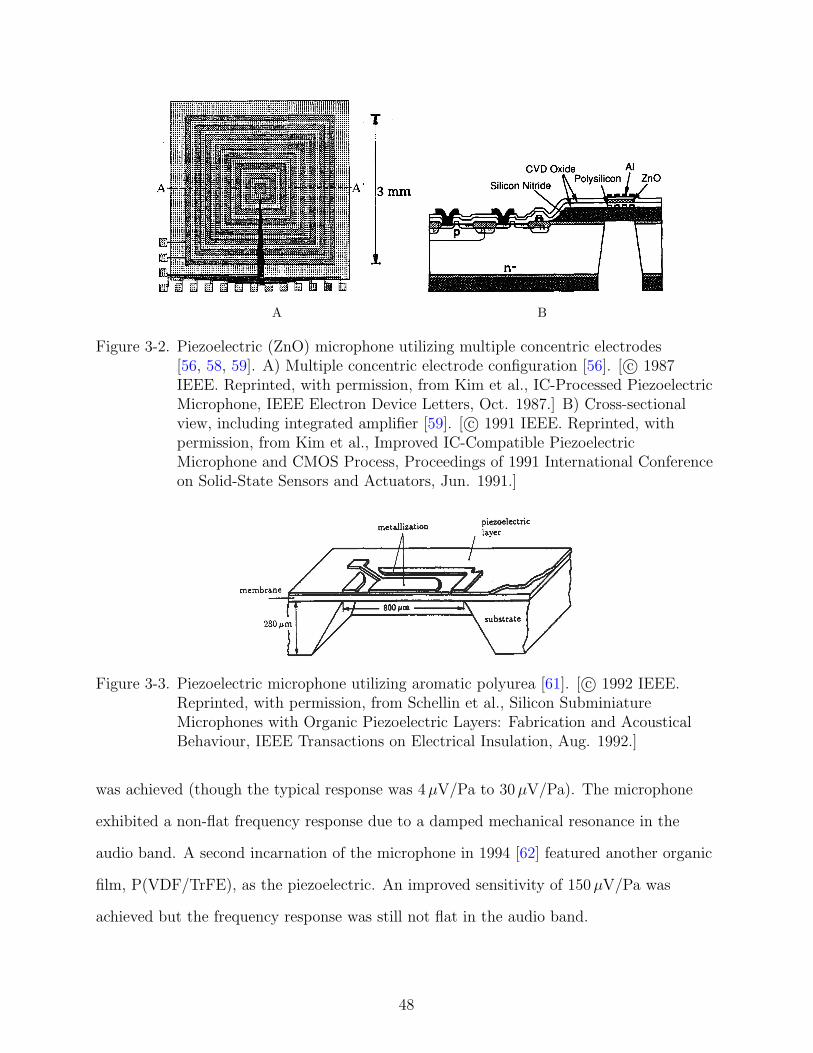
A B
Figure 3-2. Piezoelectric (ZnO) microphone utilizing multiple concentric electrodes[56, 58, 59]. A) Multiple concentric electrode configuration [56]. [ c© 1987IEEE. Reprinted, with permission, from Kim et al., IC-Processed PiezoelectricMicrophone, IEEE Electron Device Letters, Oct. 1987.] B) Cross-sectionalview, including integrated amplifier [59]. [ c© 1991 IEEE. Reprinted, withpermission, from Kim et al., Improved IC-Compatible PiezoelectricMicrophone and CMOS Process, Proceedings of 1991 International Conferenceon Solid-State Sensors and Actuators, Jun. 1991.]
Figure 3-3. Piezoelectric microphone utilizing aromatic polyurea [61]. [ c© 1992 IEEE.Reprinted, with permission, from Schellin et al., Silicon SubminiatureMicrophones with Organic Piezoelectric Layers: Fabrication and AcousticalBehaviour, IEEE Transactions on Electrical Insulation, Aug. 1992.]
was achieved (though the typical response was 4µV/Pa to 30µV/Pa). The microphone
exhibited a non-flat frequency response due to a damped mechanical resonance in the
audio band. A second incarnation of the microphone in 1994 [62] featured another organic
film, P(VDF/TrFE), as the piezoelectric. An improved sensitivity of 150µV/Pa was
achieved but the frequency response was still not flat in the audio band.
48

Figure 3-4. Piezoelectric (ZnO) microphone with cantilever sensing element [64]. [ c© 1996IEEE. Reprinted, with permission, from Lee et al., Piezoelectric CantileverMicrophone and Microspeaker, Journal of Microelectromechanical Systems,Dec. 1996.]
In 1993, Ried et al. of the Berkeley Sensor and Actuator Center extended the work
of Kim [56–59]. The new iteration [63] made use of a 2.5 mm × 2.5 mm × 3.5µm silicon
nitride structural layer with improved stress control. This layer was designed to be thick
relative to other diaphragm layers, which were fabricated at corporate partner Orbit
Semiconductor and not controlled for stresses. ZnO was again used as the piezoelectric
and large-scale integrated CMOS circuits were included on-chip. A flat frequency response
was obtained from 100 Hz–18 kHz, with a sensitivity of 0.92 mV/Pa. In 1996, Lee et
al. [64] of the same research group presented a new piezoelectric microphone with
ZnO on a low pressure chemical vapor deposition (LPCVD), low-stress silicon nitride
cantilever sensing element, pictured in Figure 3-4. The enhanced compliance of this
“cantilever diaphragm” resulted in a high sensitivity of 30 mV/Pa. However, with the
more compliant diaphragm also came a low resonant frequency and a resulting bandwidth
of only 100 Hz to 890 Hz. A later iteration [65] improved the bandwidth to 1.8 kHz while
maintaining the same sensitivity.
49

Figure 3-5. Cross section of the first aeroacoustic MEMS microphone [17]. [Reprinted withpermission of the American Institute of Aeronautics and Astronautics.]
In 1998, Sheplak et al. [16, 17] introduced the first MEMS microphone designed
specifically for aeroacoustics applications (Figure 3-5). The microphone included four
dielectrically isolated piezoresistors on top of a 210µm diameter, 0.15µm thick silicon
nitride diaphragm for sensing of diaphragm deflection. Lumped element modeling was
used to predict performance. A sensitivity of 2.24µV/Pa/V was measured to within
±3 dB from 200 Hz to the testing limit of 6 kHz, though the frequency response was
predicted to be flat up to 300 kHz. A linear response was obtained up to the testing limit
of 155 dB. The device noise floor was 92 dB/√
Hz at 250 Hz.
In 1999, Naguib et al. [66, 67] introduced two square diaphragm (510µm to 710µm
on a side) piezoresistive microphone designs for use in measuring jet screech noise.
Sensitivities of 1.2 mV/Pa/V to 1.8 mV/Pa/V were measured over a frequency range of
1.5 kHz–5 kHz. The dynamic range was not reported. In 2002, Huang et al. [68] improved
the performance of the 710µm design through the use of an improved fabrication process.
The new microphone, for which a depiction is found in Figure 3-6, yielded the highest
reported maximum linear pressure for a MEMS microphone yet reported in the literature,
174 dB. The authors were only able to confirm a flat frequency response up to 10 kHz
because of testing limitations.
50

Figure 3-6. Piezoresistive MEMS microphone for aeroacoustic measurements [68].[Reprinted, with permission, from Huang et al., A Silicon MicromachinedMicrophone for Fluid Mechanics Research, Journal of Micromechanics andMicroengineering, 2002.]
Starting in 2001, researchers at the Interdisciplinary Microsystems Group (IMG)
at the University of Florida presented a number of MEMS microphones specifically
designed for aeroacoustic measurement purposes. In 2001, Arnold et al. [18] made several
modifications to the piezoresistive microphone design of Sheplak et al. [16, 17] in order
to improve performance, particularly the MDP: the device was enlarged in order to limit
misalignment effects; noise in the piezoresistors was reduced via a reduction in resistance
and the use of higher quality wafers; a higher doping concentration was used for the
piezoresistors; and finally, a plasma-enhanced chemical vapor deposition (PECVD) silicon
nitride passivation layer was added to protect the device from moisture and reduce drift.
A micrograph of the microphone is shown in Figure 3-7. The MDP was indeed lowered to
52 dB (1 Hz bin centered at 1 kHz) and a linear response was measured up to the testing
limit of 160 dB, though the sensitivity was reduced by nearly a factor of 3. The frequency
response of this microphone was later characterized up to very high frequencies at Boeing
Corporation; it showed a flat response to within ±1 dB out to 100 kHz [19].
Aeroacoustic microphones were developed at IMG utilizing other transduction
methods as well. In 2004, Kadirvel et al. [70] described the design, fabrication, and
testing of an intensity-modulated optical MEMS microphone. The intensity noise in
the light source contributed to a high MDP of 70 dB and the device was linear only to
132 dB. In 2007, Martin et al. [71, 72] discussed a dual-backplate capacitive MEMS
51
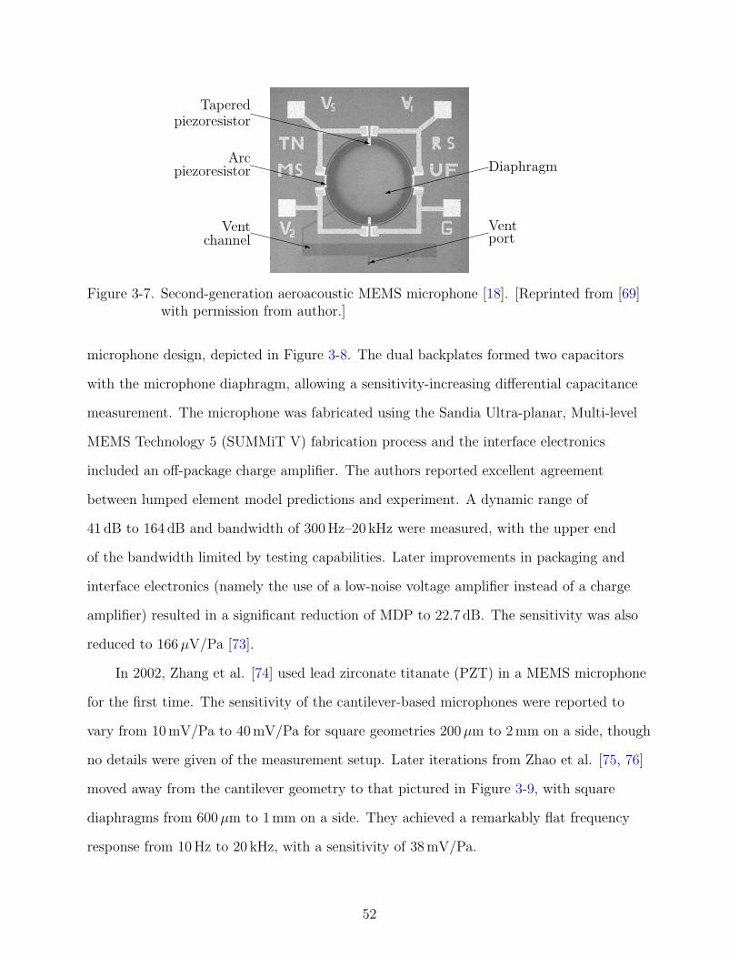
XXXXXXXXXXz
Taperedpiezoresistor
XXXXXXXz
Arcpiezoresistor
XXXXXzVent
channel9
Ventport
9
Diaphragm
Figure 3-7. Second-generation aeroacoustic MEMS microphone [18]. [Reprinted from [69]with permission from author.]
microphone design, depicted in Figure 3-8. The dual backplates formed two capacitors
with the microphone diaphragm, allowing a sensitivity-increasing differential capacitance
measurement. The microphone was fabricated using the Sandia Ultra-planar, Multi-level
MEMS Technology 5 (SUMMiT V) fabrication process and the interface electronics
included an off-package charge amplifier. The authors reported excellent agreement
between lumped element model predictions and experiment. A dynamic range of
41 dB to 164 dB and bandwidth of 300 Hz–20 kHz were measured, with the upper end
of the bandwidth limited by testing capabilities. Later improvements in packaging and
interface electronics (namely the use of a low-noise voltage amplifier instead of a charge
amplifier) resulted in a significant reduction of MDP to 22.7 dB. The sensitivity was also
reduced to 166µV/Pa [73].
In 2002, Zhang et al. [74] used lead zirconate titanate (PZT) in a MEMS microphone
for the first time. The sensitivity of the cantilever-based microphones were reported to
vary from 10 mV/Pa to 40 mV/Pa for square geometries 200µm to 2 mm on a side, though
no details were given of the measurement setup. Later iterations from Zhao et al. [75, 76]
moved away from the cantilever geometry to that pictured in Figure 3-9, with square
diaphragms from 600µm to 1 mm on a side. They achieved a remarkably flat frequency
response from 10 Hz to 20 kHz, with a sensitivity of 38 mV/Pa.
52

Figure 3-8. A dual-backplate capacitive MEMS microphone [71]. [ c©2007 IEEE.Reprinted, with permission, from Martin et al., A MicromachinedDual-Backplate Capacitive Microphone for Aeroacoustics Measurements,Journal of Microelectromechanical Systems, Dec. 2007.]
Bottom Electrode (Pt/Ti)
Si3N4 Barrier Layer
Via PZT
Top Electrode
(Pt/Ti)
Si
Bottom Electrode Top Electrode
Diaphragm
Figure 3-9. Early PZT-based piezoelectric microphone (adapted from Zhao et al. 2003[75, 76]).
The next piezoelectric microphone, pictured in Figure 3-10, was presented by Ko et
al. in 2003 [77]. The square diaphragm was formed from ZnO sandwiched between two
concentric segmented aluminum electrodes on LPCVD silicon nitride. The microphone
had a sensitivity of approximately 30µV/Pa and a resonance at 7.3 kHz.
In order to avoid residual stress issues omnipresent in silicon nitride diaphragms, Niu
and Kim [78] proposed a novel bimorph structure in 2003. The film stack was composed
53

Figure 3-10. Piezoelectric (ZnO) microphone with two concentric electrodes [77].[Reprinted from Sensors and Actuators A, vol. 103, Ko et al., MicromachinedPiezoelectric Membrane Acoustic Device, pgs. 130–134, Copyright 2003, withpermission from Elsevier.]
of ZnO, aluminum (Al) electrodes, and parylene D as the structural layer. Concentric
segmented electrodes were also used as in [56, 58, 59]. A sensitivity of 520µV/Pa was
achieved, which was an improvement over [56, 58] but not [59].
In 2003, efforts at Bruel and Kjær [79] yielded a measurement quality MEMS
condenser microphone, depicted in Figure 3-13. The design goal for the mic was to achieve
a 1/4” measurement microphone with noise characteristics near that of a traditional
1/2” Bruel and Kjær 4134 microphone (18 dB(A)). A number of stability issues were
also considered, including sensitivity to temperature, relative humidity, and static
pressure. The design featured a 1.95 mm octagonal LPCVD silicon nitride diaphragm
with chrome/gold electrodes mounted in a titanium housing. The microphone had a
dynamic range of 23 dB(A)–141 dB and bandwidth of 251 Hz – 20 kHz.
In 2004, Polcawich [80] shared development details for a PZT MEMS microphone
targeted for use in a MEMS photoacoustic spectrometer or remote acoustic sensor. The
circular diaphragm diameters ranged from 500µm to 2000µm and were fabricated in
designs with 80 % PZT coverage in the center of the diaphragm and 20 % PZT coverage on
the outside edge of the diaphragm. Sensitivities of 97.9 nV/Pa to 920 nV/Pa were reported
and resonant frequencies were O (100 kHz). No indication of the bandwidth or dynamic
range was given for these microphones.
54

Figure 3-11. Measurement-grade MEMS condenser microphone developed at Bruel andKjær [79]. [ c©2003 IEEE. Reprinted, with permission, from Scheeper et al., ANew Measurement Microphone Based on MEMS Technology, Journal ofMicroelectromechanical Systems, Dec. 2003.]
Also in 2004, Hillenbrand et al. [81] suggested the use of charged cellular polypropylene
(commercially known as VHD40) as the piezoelectric material in a microphone. They
presented results for two structures formed from single and five layer glued stacks of
metallized VHD40, which had sensitivities of 2 mV/Pa and 10.5 mV/Pa, respectively.
A total harmonic distortion of only 1% at 164 dB was reported, though it is not clear
to which of the two designs the measurement applied or how the measurement was
performed. This large maximum pressure, in addition to a large reported bandwidth up to
nearly 140 kHz for the single film design, makes this microphone potentially appealing for
use in aeroacoustic applications. However, the microphone was not batch fabricated and
concerns about the temperature stability of the charged film were noted.
Horowitz et al. (2007) [20] of IMG introduced the first — and prior to this study,
only — piezoelectric MEMS microphone designed specifically for aeroacoustic applications.
The circular microphone diaphragm was a piezoelectric (PZT) unimorph with an annular
55

A B
Figure 3-12. Piezoelectric (PZT) microphone for aeroacoustic applications [20]. [Reprintedwith permission from S. Horowitz et al., Development of a micromachinedpiezoelectric microphone for aeroacoustics applications, Journal of theAcoustical Society of America, vol. 122, pp. 34283436, Dec. 2007. c© 2007,Acoustic Society of America.]
piezoelectric film stack on a silicon layer, as shown in Figure 3-12. Lumped element
modeling was used to predict device performance. The reported maximum pressure of
169 dB exceeded the design goal of 160 dB. The frequency response could not be measured
beyond 6.7 kHz due to equipment limitations, though the resonant frequency of the
microphone diaphragm was found via a laser vibrometer measurement to be 59 kHz.
This suggested a usable bandwidth nearly sufficient for 1/4 scale model aeroacoustic
measurement applications.
Also in 2007, Fazzio et al. of Avago Technologies [82] described several microphones
produced using a variant of the FBAR (film bulk acoustic resonator) process. The circular
diaphragm was composed of AlN with molybdenum (Mo) electrodes in one of three
configurations: annular ring, inner disk, or a combination of the two. Few performance
specifications were included in the paper. The fabrication process was outlined separately
by Lamers and Fazzio [83].
Lee and Lee (2008) presented a ZnO microphone utilizing a circular diaphragm with
annular ZnO/Mo film stack. Limited characterization work was conducted. The frequency
response was not flat, with the sensitivity varying from around 1µV/Pa at 400 Hz to
56

A B
Figure 3-13. Top-view of microphone structures from Fazzio et al. (2007) [84]. A) Annularouter electrode. B) Combined circular inner and annular outer electrodes. [ c©2003 IEEE. Reprinted, with permission, from Fazzio et al., Design andPerformance of Aluminum Nitride Piezoelectric Microphones, 14thInternational Conference on Solid-State Sensors, Actuators, andMicrosystems, Jun. 2007.]
around 100µV/Pa at 10 kHz. The resonance was reported to be 54.8 kHz, so the source of
the variation was not clear.
In his 2010 doctoral dissertation from the University of Michigan, Robert Littrell
described two generations of piezoelectric microphones based on double-layered AlN/Mo
cantilevers [85]. The goal of the work was to demonstrate a low noise piezoelectric
microphone. In the first generation, an array of 20 cantilevers were used as the microphone
sensing elements, with model predictions leading to the selection of 0.5µm AlN layers.
The resulting microphones were found to have higher than expected noise floor (58 dB(A))
due to poor film quality and thus high dielectric loss. In addition, stress in the thin
films resulted in slightly curved cantilevers that reduced the vent resistance. The second
generation, with cross-section shown in Figure 3-14, featured thicker AlN layers (1µm)
for which better film quality was known to be achievable, modifications to the fabrication
process that enabled individual patterning of AlN and Mo, and reduction of the number
of cantilevers to 2 (395µm long by 790µm wide) in an effort to reduce the gap around
them and thus increase the acoustic resistance. A tested microphone had a sensitivity
of 1.82 mV/Pa, minimum detectable pressure of 37 dB(A), and 3 % THD at 128 dB. The
non-standard method used to calculate THD involved summation of harmonic amplitudes
rather than harmonic powers [47, 86, 87] and thus the distortion at 128 dB was likely
57

Si
AlNMo
Piezoelectric
Cantilevers
SiO2
Figure 3-14. Cross section of a second-generation AlN double-cantilever microphone(adapted from Littrell 2010 [85].)
over-predicted. Some stress remaining in the bottom Mo layer resulted in curvature of the
cantilever sensing elements and thus a low vent resistance that necessitated packaging the
microphones with large cavity volumes. Packaged in this way, the frequency response was
shown to be flat at least to 8 kHz, near which the plane wave tube calibration procedure
broke down due to cut-on of non-planar acoustic modes. The microphone was reported to
have a resonant frequency of 18 kHz.
Table 3-1 provides a chronological summary of piezoelectric MEMS microphones
discussed in this section, including performance data not given in the text. Due to the
myriad ways researchers present data, performance specifications collected in Table 3-1
often required interpretation; consultation of the original source is thus necessary in order
to judge the true performance of any particular microphone.
3.2 Summary
Since the first MEMS piezoelectric and aeroacoustic microphones in 1983 and 1998,
respectively, significant progress has been achieved. MEMS piezoelectric microphones
have been fabricated using a number of different materials (ZnO, AlN, polyurea, PZT,
etc.) and geometries (square and circular membranes, novel electrode configurations, etc.).
Development of MEMS aeroacoustic microphones has included the use of piezoresistive,
capacitive, optical, and piezoelectric transduction techniques and has seen steady increases
in dynamic range and bandwidth. Sufficient evidence exists to suggest that meeting the
aggressive performance specifications for a fuselage microphone is achievable.
58

Table 3-1. Summary of MEMS microphones.
Author TransductionMethod
SensingElement Size
Sensitivity DynamicRange
Bandwidth(Predicted)
Royer et al.1983 [55]
Piezoelectric(ZnO)
1.5mm*×30µm 250µV/Pa 66 dB–N/R
10Hz–10 kHz(0.1Hz-10 kHz)
Kim et al.1987 [56]
Piezoelectric(ZnO)
3mm† ×3.6µm
0.5mV/Pa 72 dB–N/R
20Hz–5 kHz
Franz1988 [60]
Piezoelectric(AlN)
0.72mm2 ×1µm#
25µV/Pa# 68 dB(A)#–N/R
N/R–45 kHz#
Kim et al.1989 [58]
Piezoelectric(ZnO)
2mm† ×↑1.4µm
80µV/Pa N/R 3 kHz–30 kHz
Kim et al.1991 [59]
Piezoelectric(ZnO)
3.04mm† ×3µm
1000µV/Pa 50 dB(A)–N/R
200Hz–16 kHz
Schellin et al.1992 [61]
Polyurea 0.8mm† ×1µm
4–30µV/Pa N/R 100Hz–20 kHz
Ried et al.1993 [63]
Piezoelectric(ZnO)
2.5mm† ×3.5µm
920µV/Pa 57 dB(A)–N/R
100Hz–18 kHz
Schellin et al.1994 [62]
Piezoelectric(P(VDF/TrFE))
1mm† × 3µm 150mV/Pa 60 dB(A)–N/R
50Hz–16 kHz.
Lee et al.1996 [64]
Piezoelectric(ZnO)
2mm‡ ×4.5µm
3mV/Pa N/R 100Hz–890Hz
Lee et al.1998 [65]
Piezoelectric(ZnO)
2mm‡ ×1.5–4.7µm
30mV/Pa N/R 50Hz–1.8 kHz
Sheplak et al.1998 [16, 17]
Piezoresistive 105µm* ×0.15µm
2.24µV/Pa·V 92dB§–155 dB
200Hz–6 kHz(100Hz–300 kHz)
Naguib et al.1999 [66, 67]
Piezoresistive 510µm† ×0.4µm
1.2µV/Pa·V N/R 1.5 kHz–5 kHz
Arnold et al.2001 [18]
Piezoresistive 500µm* ×1µm
0.6µV/Pa·V 52dB§–160 dB
1 kHz–20 kHz(10Hz–40 kHz)
Huang et al.2002 [68]
Piezoresistive 710µm† ×0.38µm
1.1mV/Pa·V 53dB§–174 dB
100Hz–10 kHz
Scheeper et al.2003 [79]
Capacitive 1.9mm* ×0.5µm
22.4mV/Pa 23 dB(A)–141 dB
251Hz–20 kHz
Ko et al.2003 [77]
Piezoelectric(ZnO)
3mm† × 3µm 30µV/Pa N/R 1 kHz–7.3 kHz
Niu et al.2003 [78]
Piezoelectric(ZnO)
3mm† ×3.2µm
520µV/Pa N/R 100Hz–3 kHz
Zhao et al.2003 [75]
Piezoelectric(PZT)
0.6–1mm† ×N/R
38mV/Pa N/R 10Hz–20 kHz
Kadirvel et al.2004 [70]
Optical 500µm* ×1µm
0.5mV/Pa 70 dB§–132 dB
300Hz–6.5 kHz(1Hz–100 kHz)
Polcawich2004 [80]
Piezoelectric(PZT)
250µm–1mm*
× 2.18µm97.9–920 nV/Pa
N/R N/R
* Radius of circular diaphragm. † Side length of square diaphragm. ‡ Side length of cantilever.§ 1 Hz bin. # Per references [62, 88]
59

Table 3-1. Continued.
Author TransductionMethod
SensingElement Size
Sensitivity DynamicRange
Bandwidth(Predicted)
Hillenbrand et al.2004 [81]
Piezoelectric(VHD40)
0.3 cm2 area ×55µm
2.2mV/Pa 37 dB(A)–164 dB
20Hz–140 kHz
0.3 cm2 area ×275µm
10.5mV/Pa 26 dB(A)–164 dB
20Hz–28 kHz
Martin et al.2007[71, 72, 89]
Capacitive 230µm* ×2.25µm
390mV/Pa 41 dB§–164 dB
300Hz–20 kHz
Horowitz et al.2007 [20]
Piezoelectric(PZT)
900µm* ×3µm
1.66µV/Pa 35.7 dB§
(95.3 dB(A))– 169 dB
100Hz–6.7 kHz(100Hz–50 kHz)
Fazzio et al.2007 [82]
Piezoelectric(AlN)
350µm* ×1.44µm
N/R 60 dB–155 dB
1 kHz-6 kHz
Lee et al.2008[90]
Piezoelectric(ZnO)
1mm × 1µm 1µV to 100µV N/R <1 kHz
Martin et al.2008 [73]
Capacitive 230µm* ×2.25µm
166µV/Pa 22.7 dB§–164 dB
300Hz–20 kHz
Littrell 2010[85]
Piezoelectric(AlN)
0.62mm2¶
2.3µm1.82mV/Pa 37 dB(A)–
128 dB50Hz–8 kHz(18.4 kHz)
* Radius of circular diaphragm. § 1 Hz bin. ¶ 2 cantilevers
Referring to Table 3-1, the performance of several prior microphone designs approach
the benchmarks set for this study. The microphones of Martin et al. [21, 72, 73] and
Hillenbrand et al. [81] possessed strong performance but the fundamental ability of the
underlying technologies to withstand the harsh high-altitude environment on an airplane
fuselage is questionable. In the case of Martin et al., the capacitive transduction method
is highly susceptible to failure from moisture shorting the electrodes, in addition to not
being a passive technology. Meanwhile, the charged cellular polypropylene film utilized by
Hillenbrand et al. has noted temperature stability problems that require further material
development [81]; it was also not batch-fabricated [91].
The microphones of Huang et al. [68] and Horowitz et al. [20] also come close to
meeting the design goals for this work with better promise of robustness. The former has
the highest reported maximum linear pressure (174 dB) but also a correspondingly high
noise floor (53 dB/√
Hz); meanwhile, the latter has a lower noise floor (47.8 dB/√
Hz)
but the maximum pressure (169 dB) obtained from measurements is also lower than
60

desired. Neither frequency response was experimentally confirmed to be flat over the
entire audio range. Kulite microphones already deployed in fuselage arrays utilize the
same piezoresistive technology as Huang et al. [68], and thus the primary advantage of the
piezoelectric microphone of Horowitz et al. [20] is its passivity.
The microphone of Horowitz et al. [20] proved a piezoelectric MEMS microphone
is a viable technology for obtaining performance near that needed for deployment in a
fuselage array. However, improvements are required to meet the performance objectives
in Chapter 1. The microphone of [20] was not designed using optimization techniques
and thus it is unlikely that performance was maximized. In this study, a system-level
model of the piezoelectric fuselage microphone is developed in Chapter 5 and used to
produce optimal microphone designs in Chapter 6. In addition, the choice of geometry
and materials — particularly the piezoelectric material — provide additional avenues for
improved performance. These choices are addressed in the next chapter, Chapter 4.
61
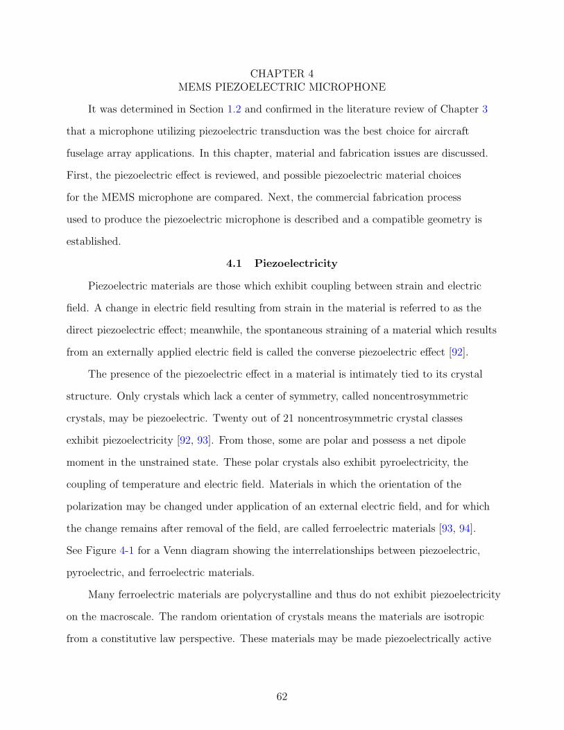
CHAPTER 4MEMS PIEZOELECTRIC MICROPHONE
It was determined in Section 1.2 and confirmed in the literature review of Chapter 3
that a microphone utilizing piezoelectric transduction was the best choice for aircraft
fuselage array applications. In this chapter, material and fabrication issues are discussed.
First, the piezoelectric effect is reviewed, and possible piezoelectric material choices
for the MEMS microphone are compared. Next, the commercial fabrication process
used to produce the piezoelectric microphone is described and a compatible geometry is
established.
4.1 Piezoelectricity
Piezoelectric materials are those which exhibit coupling between strain and electric
field. A change in electric field resulting from strain in the material is referred to as the
direct piezoelectric effect; meanwhile, the spontaneous straining of a material which results
from an externally applied electric field is called the converse piezoelectric effect [92].
The presence of the piezoelectric effect in a material is intimately tied to its crystal
structure. Only crystals which lack a center of symmetry, called noncentrosymmetric
crystals, may be piezoelectric. Twenty out of 21 noncentrosymmetric crystal classes
exhibit piezoelectricity [92, 93]. From those, some are polar and possess a net dipole
moment in the unstrained state. These polar crystals also exhibit pyroelectricity, the
coupling of temperature and electric field. Materials in which the orientation of the
polarization may be changed under application of an external electric field, and for which
the change remains after removal of the field, are called ferroelectric materials [93, 94].
See Figure 4-1 for a Venn diagram showing the interrelationships between piezoelectric,
pyroelectric, and ferroelectric materials.
Many ferroelectric materials are polycrystalline and thus do not exhibit piezoelectricity
on the macroscale. The random orientation of crystals means the materials are isotropic
from a constitutive law perspective. These materials may be made piezoelectrically active
62

Piezoelectric
Pyroelectric
Ferroelectric
Figure 4-1. Venn diagram for piezoelectric, pyroelectric, and ferroelectric materials.
through a process called poling. In this process, the materials are heated, and a strong
external electric field is applied that causes the polarization direction within the materials
to reorient. After reduction of temperature and removal of the external field, the new
polarization orientation remains and the piezoelectric effect is macroscopically active.
During this process, symmetry in the direction of poling is destroyed and the resulting
material is transversely isotropic [92]. The poled direction is referred to as the 3-direction
in the local material coordinate system.
The constitutive equations of linear piezoelectricity are given in “compressed matrix”
(or “abbreviated subscript”) form in the nomenclature of the IEEE standard as [95, 96]
Di =diqTq + εTijEj (4–1)
and Sp =sEpqTq + djpEj, (4–2)
where i, j = 1 . . . 3 and p, q = 1 . . . 6. In these equations, Di are the three components
of the electric displacement, diq are the 18 piezoelectric strain constants, Tq are the six
mechanical stresses, εTij are the six electrical permittivities, Ej are the three components
of the electric field, Sp are the six engineering (not tensoral) strains, and sEpq are the
36 elastic compliance components. Symmetry considerations for a material reduce the
number of independent diq, Sp, and sEpq. The superscripts T and E indicate that the
material properties must be measured under conditions of constant stress and electric
63

field, respectively [96]. In the absence of piezoelectric coupling, all d coefficients are
zero, and the constitutive equations reduce to those for purely dielectric [97] and linear
elastic [92, 98] materials, respectively. A second convenient form of the linear constitutive
equations is [92, 95, 96]
Di =eiqSq + εSijEj (4–3)
and Tp =cEpqSq − eTjpEj, (4–4)
where cEpq =sE−1
pq (4–5)
are the 36 elastic stiffness components,
eiq = dipcEpq (4–6)
are the 18 piezoelectric stress constants [96], and
εSij = εTij − eiqdjq (4–7)
are the permittivity components measured under constant strain [96].
Piezoelectric materials used in microsystems include lead zirconium titanate (PZT),
zinc oxide (ZnO), aluminum nitride (AlN), aromatic polyurea, polyvinylidene fluoride
(PVDF), and others. PZT is the most popular due to large piezoelectric coefficients. It is
a ferroelectric material that requires poling and is available in polycrystalline, textured,
and epitaxial thin films [93].
AlN and ZnO offer significantly lower piezoelectric coefficients than PZT, but
their dielectric properties still make them attractive materials for some applications. In
bending mode sensors that utilize the d31 coefficient, for instance, a figure of merit is the
64
piezoelectric “g” coefficient1 [94],
g31 =d31
ε33,rε0, (4–8)
which is representative of the open circuit electric field per applied mechanical stress.
Because AlN and ZnO possess significantly lower permittivities than PZT, their g31
coefficients are actually both superior.
AlN and ZnO are both pyroelectric, but not ferroelectric, and thus cannot be
poled [93, 94]; they must instead be oriented appropriately during deposition. ZnO
has traditionally been the material of choice for MEMS piezoelectric microphones (see
Section 3.1) due to the difficulty of depositing AlN films [99] and thus better availability
of ZnO [100]. The situation has been rectified with the advent of modern magnetron
sputtering tools [100–102], and it has been recognized that AlN holds several advantages
over ZnO. Zinc is a fast-diffusing ion that presents problems for integration with silicon
semiconductor processing [93, 100]. In addition, with a bandgap of 3 eV, ZnO is really a
semiconductor and there is always risk that inadvertent doping could degrade its dielectric
properties, i.e. result in a high dielectric loss [93, 100, 103]. It is thus difficult to obtain
ZnO films with high resistivity [100].
The dissipation qualities of a piezoelectric are an important consideration when
comparing material choices for piezoelectric sensors. Low resistivity (high dielectric loss) is
especially crippling in low-frequency sensors, for instance below 10 kHz [100]. Lossiness is
typically characterized via the electric loss tangent [97],
tan δ =σ
ωε33,rε0, (4–9)
where σ is the electrical conductivity and ω is the radial frequency. The loss tangent
represents the ratio of dissipated power to stored power in a dielectric. The presence of
1 Compare this to the expression for open circuit sensitivity for the pieozelectric microphone, Equa-tion 5–35.
65

dissipation introduces noise, and thus tan δ plays a role in determining the signal-to-noise
ratio of piezoelectric sensors. A figure of merit is [100],
d31
(sE11 + sE12)√
ε0ε33,r tan δ, (4–10)
which represents the intrinsic signal-to-noise ratio of the material. AlN outperforms ZnO
in this regard, with both a lower loss tangent and higher intrinsic signal-to-noise ratio. A
comparison of typical material properties and the discussed figures of merit for PZT, AlN,
and ZnO are given in Table 4-1.
Table 4-1. Typical properties of piezoelectric materials in MEMS.†
PZT‡ AlN ZnO
Properties E [GPa] 76 345 127ρ [103 kg/m3] [20] 7.7 3.26 5.6d31 [pm/V] -274 -2 -5.4d33 [pm/V] 593 5 11.7e31 [C/m2] -6.5 -0.6 -0.6e33 [C/m2] 23.3 1.6 1.3ε33,r 1470 8.5 9.2tan δ [93, 100] 0.01–0.03 0.003 0.01–0.1
Figures of Merit |g31| [V/m/Pa] 0.018 0.027 0.07
|d31|/(
sE11 + sE12)√
ε0ε33,r tan δ [105 Pa1/2] 11.7–20.3 21.4 4.3–13.5
† Material properties drawn from [104] unless otherwise noted ‡ PZT-5H [92, 96]
AlN was selected as the material for use in the piezoelectric microphone due to its
relatively high g31 coefficient and best signal-to-noise ratio among the common thin-film
piezoelectric materials. In the next section, the commercial process used to fabricate the
microphones and the role it played in early design choices is discussed.
4.2 Design for Fabrication
A partnership was formed with Avago Technologies of Fort Collins, CO for fabrication
of the piezoelectric MEMS microphone using a variant of their film bulk acoustic resonator
(FBAR) process [82, 83, 105]. An FBAR is an electromechanical filter that utilizes
the resonance of bulk acoustic waves excited in a thin piezoelectric film [106]. FBAR
66

Figure 4-2. FBAR-variant process film stack.
duplexers and filters for cellular phones have been produced in volume using the FBAR
process since 2002 [101] and Avago Technologies remains the world’s only “high volume
producer of thin-film AlN products” [83]. They are by far the most successful piezoelectric
MEMS products on the market [103].
A depiction of the film stack used in the modified FBAR process of Avago Technologies
is shown in Figure 4-2. It is composed of passivation, electrode, piezoelectric, and
structural layers; all but the latter are components of the standard FBAR process. A
key reason AlN was chosen over ZnO in the original FBAR process development was
because of its better semiconductor process compatibility [101]. The electrode material in
the film stack of Figure 4-2, molybdenum (Mo), was subsequently selected because it was
a stiff, low-loss acoustic material with high conductivity and compatible etch chemistry
with AlN [101, 106]. As proprietary features of the FBAR-variant process, the materials
used in the passivation and structural layers are not disclosed. A deep reactive ion etch
(DRIE) forms a cavity underneath the diaphragm in Figure 4-2.
The performance of microphones with thin film diaphragms is extremely sensitive
to film stress, while the first priority in FBAR fabrication is piezoelectric film thickness
uniformity [83]. Leveraging the FBAR process, therefore, requires renewed attention to
film stress. Thin films are susceptible to developing both intrinsic and extrinsic residual
67

stresses. Thermal expansion mismatch between films, substrate, and package lead to
thermal stress, the most common extrinsic stress. Intrinsic stresses can be caused by a
variety of factors, including lattice mismatch, impurities, volume change processes (e.g.
phase transformation or outgassing), or atoms being trapped in high-energy configurations
[107, 108]. The amount of stress control varies by process; sputter deposition (common for
AlN), for instance, is a complex process that does afford some flexibility to tailor stresses.
Customization of the stress state is achieved via adjustment of bias power, argon pressure,
sputtering gas mass, temperature, and/or deposition rate [108]. Avago Technologies is able
to adjust film deposition parameters to target a large range of film stresses.
The FBAR-variant film stack provided some flexibility in the selection of microphone
geometry. With a DRIE step already integrated into the FBAR-variant process — as
opposed to an anisotropic release etch — the diaphragm was not limited to rectangular
geometry [90, 109]. A circular diaphragm offers several advantages over rectangular
geometries: it is easier to model/design since first-mode vibrations can be reduced to a
1-D axisymmetric problem, as opposed to a 2-D problem in the rectangular case; it lends
itself to simpler electrode configurations over the rectangular case, in which high stress
regions are not uniformly distributed along the boundary [90]; and the circular geometry
does not inherently include lifetime-reducing stress concentrations.
Clamped circular diaphragms possess high stress/strain regions both along the
circumference and at the center. The configuration of the piezoelectric/electrode films
on the structural layer therefore presents another design choice [110]. A single stack of
piezoelectric/electrode films presents the least complexity; two such configurations are
shown in Figure 4-3. Figure 4-3A shows the piezoelectric/electrode stack in the middle of
the diaphragm, called here the “central disc” configuration, while Figure 4-3B shows the
stack as an “outer annulus.” Concerns about the contribution of electrode traces running
over the diaphragm in the former case, particularly their potential contribution to device
68

A B
Figure 4-3. Potential circular diaphragm piezoelectric/metal film stack configurations. A)Central disc. B) Outer annulus.
stiffness and parasitic capacitance and the possibility that they could promote asymmetric
modal vibrations [20, 111], led to the choice of the annular configuration.
Although exact FBAR process details are proprietary, a general outline of fabrication
steps for a microphone structure was published by Avago Technologies [82, 83] and is
summarized in Figure 4-4. The process involved both surface and bulk micromachining,
starting with a 675µm thick, 150 mm (6”) silicon wafer (Figure 4-4A). First, a shallow
cavity was etched and filled with sacrificial material, which served to define the diaphragm
diameter and set an etch stop for subsequent backside processing. The wafer surface
was thinned to 500µm and planarized via chemical-mechanical polishing (CMP) as in
Figure 4-4B. The structural, metal, piezoelectric, and passivation layers, in addition to
the bond pads, were then deposited and patterned in a set of proprietary process steps
(Figure 4-4C). What is known from the open literature about the film deposition is
that AlN is typically sputter-deposited [100–103], often at low temperatures (<200 C).
Possible etch chemistries for AlN and Mo include chlorine and fluorine gas, respectively
[101]. Projection step-and-repeat photolithography [43] was used to repeat the same 10 ×
10 pattern of microphones (with die 2 mm on a side) over the entire wafer. A DRIE from
the backside of the wafer formed the back cavity (Figure 4-4D) and the sacrificial material
was removed to release the diaphragm (Figure 4-4E).
69

A Begin with a bare silicon wafer.
Sacrificialmaterial
B Etch cavity in silicon wafer and deposit sacrificialmaterial. Perform CMP.
*Structural
-AlNHHjPassivation ) Mo
+
C Deposit and pattern films.
`
D DRIE through backside and stop on sacrificiallayer.
`
E Release the diaphragm via removal of sacrificiallayer.
Figure 4-4. Outline of fabrication steps.
4.3 Summary
In this chapter, material and fabrication-related issues relevant to the piezoelectric
MEMS microphone were discussed. First, the relative merits of common thin-film
piezoelectric materials were reviewed, and the material choice of AlN was established.
Next, a microphone geometry utilizing an annular piezoelectric film stack and compatible
with the selected fabrication process was chosen. Finally, the proprietary FBAR-variant
fabrication process was described via reference to open literature on the subject. With the
microphone geometry and composition firmly established, the next chapter focuses on the
development of a model to predict its performance.
70

CHAPTER 5MODELING
In this chapter, a multiple-energy-domain dynamic model of the piezoelectric
microphone is developed that allows computation of performance metrics such as
sensitivity, bandwidth, and minimum detectable pressure. First, an overview of the
lumped element modeling technique is given. Next, an overall lumped element model of
the microphone is introduced and predictive models for its component parts are discussed
in turn. With the lumped element model established, several important quantities,
including the open circuit frequency response function of the microphone and the overall
electrical impedance, are derived. The need for interface electronics and their impact on
system response is then addressed. Finally, two architectures for interface electronics — a
voltage amplifier and charge amplifier — are integrated with the lumped element model
and their relative merits are discussed in terms of sensitivity and minimum detectable
pressure.
5.1 Lumped Element Modeling Overview
A piezoelectric microphone converts energy between the acoustic and electrical
energy domains. Accurate prediction of its behavior requires physics-based models that
capture the underlying transport of energy. Unfortunately, exact analytical solutions to
governing differential equations coupling multiple energy domains are rarely available
[112]. Numerical solutions to these equations using techniques such as the finite element
method are possible, but are often computationally intensive and do not readily provide
physical insight [43]. Therefore, a compromise in fidelity in exchange for efficient and
physically insightful models is warranted; this is the overriding reason for the use of the
lumped element modeling technique.
When the wavelength of a physical phenomenon being measured is much greater than
the characteristic length scale (λ ≫ L) of the sensor itself, spatial and temporal variations
of the physical phenomenon may be decoupled [113]. A microphone, for instance, which
71

has a sensing element much smaller than the wavelength of incident acoustic waves sees
a distribution of pressure which is essentially uniform. Although the pressure continues
to change with time, the changes are effectively felt everywhere on the microphone
diaphragm at the same instant [35]. For an acoustic signal at a frequency of 20 kHz,
λ = 17 mm in air and the diaphragm diameter must be much less than λ.
Under the condition λ ≫ L, the distributed energy storage mechanisms of the true
system may be lumped into equivalent energy storage elements, called “lumped elements.”
In the mechanical domain, this means a distributed system with infinite degrees of
freedom may be represented by an equivalent single-degree-of-freedom mass-spring-damper
system. Generalized kinetic energy is stored in a lumped mass, generalized potential
energy is stored in a lumped compliance (inverse of spring stiffness), and energy is
dissipated in a lumped damper. The lumped elements may be found via a truncated
series expansion of the complex impedance [28]. Alternatively, they may be found from
equating the energy storage of the true system (using the static solution to approximate
the dynamic one) with the energy storage in the ideal lumped elements. The resulting
single-degree-of-freedom representation is then valid up to and just beyond the first
resonant frequency of the true system [114].
Convenient analogies exist between the mechanical/acoustic domains and the
electrical domain. A mass-spring-damper system may be represented by an equivalent
LCR circuit in which an inductor is analogous to a mass, a capacitance is analogous to
a compliance, and a resistor is analogous to a damper [43]. This analogy is illustrated in
Figure 5-1. The conjugate power variables in the electrical domain, voltage (an “effort
variable”) and current (a “flow variable”), are then analogous to force and velocity in
the mechanical domain or pressure and volume velocity in the acoustic domain. These
so-called conjugate power variables may be defined in each energy domain [43].
The circuit analogy, in conjunction with lumped element modeling, may be
employed to produce a system-level model in which the lumped elements, including those
72

M
R
k=1/C
F
x
A
F
xM
R C
B
Figure 5-1. Illustration of the electrical-mechanical analogy. A) Mass-spring-dampersystem. B) Inductor-capacitor-resistor circuit.
representative of different energy domains, are all interconnected in a way that captures
the energy exchange of components in the true system. Techniques developed for circuit
analysis then become available, as well as the intuitive understanding of circuit diagrams
that many engineers share. The end result is an insightful, efficient, and acceptably
accurate model of a multiple-energy-domain system.
The lumped element modeling technique and equivalent circuit representations have
historically been used in the field of electroacoustics [35, 114, 115] and have found use in
the design of microelectromechanical systems (MEMS) transducers [17, 20, 21, 116]. The
technique is utilized in this study to perform model-based design.
5.2 Lumped Element Model of a Piezoelectric Microphone
In this section, a system-level lumped element model of the piezoelectric MEMS
microphone is produced. The development is similar to Horowitz et al. (2007) [20], with
extensions to the underlying mechanical modeling. The cross section of the piezoelectric
microphone structure considered in this study is shown in Figure 5-2. It includes a
diaphragm, which deflects under an incident acoustic pressure; a cavity, which allows the
diaphragm to move; and a vent, which connects the cavity to the ambient environment
and thereby eliminates sensitivity to static pressure changes. As the diaphragm deflects,
strain in the piezoelectric layer yields an electric field due to the direct piezoelectric effect.
The electric field is sensed as a voltage difference across the electrodes — this is the
microphone output.
73

In a general design setting, much flexibility exists in the selection of piezoelectric
microphone geometry and film stack composition, but a piezoelectric microphone
diaphragm must at minimum include a set of electrodes and a piezoelectric layer. The
microphone in this study is composed of thin-film materials dictated by the FBAR-variant
fabrication process as described in Section 4.2; these include an aluminum nitride (AlN)
piezoelectric layer, molybdenum (Mo) electrodes, and structural and passivation layers for
which the proprietary material choices are not disclosed.
`
Diaphragm
,ad ad radM M+
,ad ad radR R+
adC
Cavity
acM acC
Vent
avR
0v+
-
esR
rz
1r a=
2r a=
3r a=Piezoelectric layer
Top electrode
Bottom electrode
Passivation layer
Structural layer
ebCepReoC
Figure 5-2. Piezoelectric microphone structure.
Lumped element modeling was introduced as an efficient and simple technique for
estimating the behavior of transducers. In Figure 5-2, the lumped elements that represent
each of the microphone’s major components are identified based on the underlying physics
of each. To avoid confusion, the convention used here is that the first subscript on an
element stands for the domain (acoustic or electrical) and the second subscript provides
identification. For instance, Mad is the lumped diaphragm mass in the acoustic domain.
Each of the elements found in Figure 5-2 are connected in an equivalent circuit
as shown in Figure 5-3. The diaphragm is modeled as a lumped mass and compliance,
Mad and Cad, respectively [113]. Damping is included as a resistance, Rad, that accounts
for loss mechanisms such as thermoelastic dissipation [117] and anchor/support loss
[118]. Coupling between the diaphragm and the air on the free side is modeled using a
74

CacMac
Rav
Rad +Rad,rad
Mad +Mad,rad
Cad
p
φa : 1
Ceb Ceo Rep
Res
+
−
vo
Figure 5-3. Piezoelectric microphone lumped element model.
radiation mass Mad,rad and resistance Rad,rad that are connected in series with Cac and
Mad because they all experience the same volume velocity. The cavity is modeled as a
mass and compliance, Mac and Cac, respectively. The vent is represented as a resistance
Rav. Just as in Figure 5-2, the placement of Rav in Figure 5-3 provides an alternate path
for volume velocity, and thus a pressure drop, between the ambient environment and the
back cavity. Coupling between the acoustical and electrical domains is captured using
a transformer with turns ratio φa. Electrical elements are connected on the right side
of Figure 5-3 and include the sense capacitance Ceb, the parasitic capacitance due to
electrode overhang beyond the diaphragm Ceo, piezoelectric loss resistance Rep, and series
resistance Res. The “b” in Ceb stands for “blocked,” meaning it is the capacitance that
remains when the piezoelectric is blocked from motion (and thus no volume velocity flows
into the transformer). The element Res represents the resistance of any leads or wires on
or connecting to the microphone. The microphone output is the voltage vo.
Although the impedances of each component of the microphone are introduced
here as combinations of masses/ inductances, compliances/ capacitances, and dampers/
resistances, it is sufficient at this stage to recognize that each component possesses an
impedance and that the form of the impedance is dictated by the associated physics. The
origins of each impedance are discussed in the next sections.
75

5.2.1 Elements
In this section, the various elements included in the lumped element model for the
piezoelectric MEMS microphone are discussed in turn. First, modeling of the piezoelectric
transduction is discussed. Next, structural elements that represent the diaphragm are
defined and the associated underlying diaphragm mechanical model is outlined. Acoustical
and electrical elements are then examined.
5.2.1.1 Transduction
Modeling the transduction of the piezoelectric microphone requires a knowledge
of the constitutive behavior of piezoelectric materials. The 3-D constitutive equations
[95, 96] were discussed in Section 4.1 and may be written compactly, denoting vectors and
matrices with bold symbols, as
D
S
=
εT d
dT sE
E
T
. (5–1)
The 1-D, time-harmonic equivalent of Equation 5–1 is [20, 113]
I
q
=
jωCef jωda
jωda jωCad
V
p
, (5–2)
where I is current, q = jω∆∀ is volume velocity, ∆∀ is volume displacement, V is
voltage, and p is pressure. The quantities Cef , da, Cad, φa, and Ceb all serve as constitutive
properties of the piezoelectric and are defined in turn in the coming paragraphs. It may
be shown using circuit analysis techniques that a transformer in the configuration of
Figure 5-4 is equivalent to Equation 5–2 given appropriate definitions for φa and Ceb.
Thus, just as Equation 5–2 couples the acoustic and electrical domain, so too does the
two-port electroacoustic circuit element of Figure 5-4. As used in the lumped element
model of Figure 5-3, this element couples the diaphragm/cavity/vent response to the
electrical response of the piezoelectric.
76

φa : 1
Cad
q
−
+
p Ceb
I
−
+
V
Figure 5-4. Two-port piezoelectric transduction element.
The capacitance of the annular film stack is composed of a sense capacitance that
contributes to the transduction and a parasitic capacitance due to electrode overhang
beyond the stressed diaphragm region. The electrical free capacitance Cef , i.e. the
capacitance observed when the diaphragm is free to move, is simply the parallel plate
capacitance between the electrodes [35],
Cef =ǫAe
hp
. (5–3)
Here, ǫ is the absolute permittivity of the piezoelectric layer, Ae = π (a22 − a21) is the
electrode area, and hp is the distance the electrodes are separated by the piezoelectric
layer. It is related to the electrical blocked capacitance Ceb as [35, 113]
Ceb =(
1 − k2)
Cef , (5–4)
where k is the electromechanical coupling factor defined from
k2 =d2a
CefCad
, (5–5)
which is representative of the efficiency of energy conversion from one domain to the other,
though losses are not accounted for [35]. The diaphragm compliance Cad is defined from
Equation 5–2 as
Cad =∆∀|V=0
p, (5–6)
so the diaphragm compliance in the transduction representation of Figure 5-4 is the
volume displacement per pressure under short-circuit conditions, called the short-circuit
77

compliance [35]. Calculation of Cad from Equation 5–6 is related to the structural model
of the diaphragm that is discussed further in Section 5.2.1.2.
Two definitions for the acoustic piezoelectric coefficient da may be extracted from
Equation 5–2. The first is
da =Q|V=0
p, (5–7)
where Q is the electric charge, which is related to the current as I = jωQ. The second
definition is
da =∆∀|p=0
V. (5–8)
The choice of which of Equations 5–7 to 5–8 to use for calculation of da is dictated by the
ease of calculating the quantities Q or ∆∀ from a mechanical model of the diaphragm;
their equality, or reciprocity, is implied from the linear piezoelectric constitutive relations.
Finally, the turns ratio of the transformer (or transduction factor) is defined as [20, 113]
φa = − daCad
. (5–9)
5.2.1.2 Structural elements
Using the lumped element method, the electromechanical behavior of the diaphragm
is captured in a series of elements. The distributed mass and compliance of the diaphragm
are collected, or “lumped” into an acoustic mass Mad and compliance Cad that together in
series with the acoustic damping Rad form the impedance of the diaphragm. Taken alone,
these elements are sufficient to represent the diaphragm as a single-degree-of-freedom
system. However, the piezoelectric transduction mechanism is integrated directly with
the diaphragm and the effective piezoelectric coefficient da is also dependent on the
diaphragm’s electromechanical behavior. To determine the values of these elements for a
given diaphragm configuration, predictive capabilities are needed.
First, however, it is expedient to define each of the elements under the assumption
that a prediction for the static transverse diaphragm displacement, w (r), due to a
78

pressure or voltage input is available. With w (r) known, the volume displaced by the
diaphragm is defined as its area integral, i.e.
∆∀ =
∫ a2
0
w (r) 2πrdr. (5–10)
Equation 5–10 may be used to compute the acoustic compliance Cad or the acoustic
piezoelectric coefficient da per Equations 5–6 and 5–8.
The lumped mass of the diaphragm in the acoustic domain is found from equating
the kinetic energy of the lumped mass to the actual, distributed kinetic energy of the
diaphragm. This equality is given as
1
2Mad (jω∆ ∀|V=0)
2 =1
2
∫
∀
ρ [jω w (r)|V=0]2 d∀, (5–11)
where the volume velocity q and actual plate velocity w (r) are assumed time harmonic.
The stipulation that V = 0 is made because pressure, not voltage, is the effort variable for
this element. Solving Equation 5–11 while making use of Equation 5–6 yields
Mad =
a2∫
0
ρA w (r)|2V=0 2πrdr
∆∀|2V=0
, (5–12)
where ρA [kg/m2] is the aerial density of the diaphragm,
ρA(r) =
∫ zt
zb
ρ(r, z)dz, (5–13)
and zb and zt are the top and bottom z-coordinates of the diaphragm, respectively.
Making use of Equation 5–6, Mad is equivalently written as [20, 113]
Mad =2π
C2ad
a2∫
0
ρA
(
w (r)|V=0
p
)2
rdr, (5–14)
which though awkwardly suggesting Mad is directly dependent on compliance and
pressure, is convenient for performing calculations.
79

Finally, the lumped resistance Rad is related to the classical damping coefficient ζ as
[34]
Rad = 2ζ
√
Mad
Cad
. (5–15)
The damping coefficient is usually determined experimentally because of the difficulty of
both predicting what damping mechanisms are important and modeling their effects. In
this study, ζ = 0.03 — representative of an observed value for a similar device [119] — is
assumed.
With the lumped elements associated with the diaphragm defined and the need for
prediction of w (r) motivated, Section 5.2.2 details the model implementation for this
study. First, however, the remaining lumped elements are defined.
5.2.1.3 Acoustic elements
In this section, lumped elements capturing the impact of the presence of fluid in
and around the microphone are defined. These include impedances associated with fluid
external to the microphone, Rad,rad and Mad,rad, fluid within the back cavity, Cac and Mac,
and fluid in the vent, Rav. In each of these elements, the gas density ρ0 and isentropic
speed of sound c0 appear regularly, in addition to the acoustic wave number k = ω/c0.
The product ρ0c0 is known as the characteristic impedance of the fluid medium, Z0.
The diaphragm re-radiates sound to the surrounding fluid as it vibrates, and this
interaction with the fluid impacts the diaphragm dynamics. The so-called Rayleigh
integral [28] governs the relationship between the vibrations of a “piston” in a rigid baffle
(representative of the microphone diaphragm) and the radiated pressure field. It may be
solved numerically for an arbitrary piston modal vibration, but in the interest of simplicity
and computational efficiency, the classical solution for a rigid circular piston moving
with uniform velocity is leveraged to predict the effect of the fluid on the diaphragm.
The diaphragm and a rigid circular piston as radiators are similar in character, with the
fundamental difference being that the piston moves as a rigid body with a single velocity,
while the diaphragm does not. The acoustic radiation impedance of a rigid circular piston
80

with an undetermined effective radius — not equal to the radius of the circular diaphragm
— is [28]
Z =Z0
πa2eff
[
1 − 2J1 (2kaeff )
2kaeff+ j
2K1 (2kaeff )
2kaeff
]
, (5–16)
where J1 is the first-order Bessel function of the first kind and K1 is the first-order Struve
function.
To find the effective radius aeff , the volume velocity of the diaphragm,
q = jω∆∀|V=0 , (5–17)
is equated to the volume velocity of an equivalent circular piston moving with the center
velocity of the diaphragm,
q = jωw (0)|V=0 πa2eff . (5–18)
Solving for aeff then yields
aeff =
√
1
π
∆∀|V=0
w (0)|V=0
, (5–19)
from which the effective area Aeff = πa2eff may also be calculated. For a given diaphragm
geometry, a circular piston of radius aeff and corresponding area Aeff therefore produces
the same volume displacement and should have the same approximate radiative properties.
In the low-frequency approximation (kaeff ≪ 1), obtained by performing a Maclaurin
series expansion of Equation 5–16 and dropping terms of order (kaeff )3 and higher, the
radiation impedance of air reduces to a mass [28],
Ma,rad =8ρ0
3π2aeff, (5–20)
and a resistance,
Ra,rad =ρ0ω
2
2πc0. (5–21)
These quantities capture the effects of air particles moving together with the diaphragm
and the loss of acoustic energy into the surrounding medium. This low-frequency
approximation of Equation 5–16 is valid to within 5% up to approximately ka = 0.43.
81

The fluid in the cavity behind the diaphragm also impacts its dynamics. The cavity
impedance is derived from the classical acoustics solution for the acoustic impedance of a
rigid-walled tube with a rigid termination [28],
Zac = −jZ0
Ac
cot (kdc) , (5–22)
where Ac is the cavity area and dc is the cavity depth. When the acoustic wavelength
is much less than the length of the tube, a truncated series expansion yields an acoustic
compliance,
Cac =∀c
ρ0c20, (5–23)
where ∀c = dcAc is the cavity volume, and an acoustic mass,
Mac =ρ0∀c
3A2c
. (5–24)
For kdc ≤ 0.3, the contribution of Mac to the cavity impedance is less than 3% of the
contribution of Cac and it may be neglected. However, it is retained because its inclusion
adds little additional complication to the model. The FBAR-variant process makes use of
silicon wafers that are 500µm thick following the chemical-mechanical polish step, yielding
dc = 500µm. As an example, for this cavity at 20 kHz, kdc = 0.18.
Finally, the flow through the vent channel is modeled as fully developed, pressure
driven flow between two parallel surfaces [43, 120]. The canonical vent structure has a
length Lv and a rectangular cross section of height hv and width bv, with bv ≫ hv. This
thin channel runs from the cavity underneath the diaphragm and emerges topside through
a circular hole in the film stack. The impedance of the vent is simply the resistance, [43]
Rav =12µLv
bvh3v
, (5–25)
where µ is the viscosity of the fluid. For the FBAR-variant fabrication process, Lv =
50µm, hv = 2µm, and bv = 25µm.
82

5.2.1.4 Electrical elements
Electrical elements found in the lumped element model represent the capacitance
of the piezoelectric film stack (Ceb), a parasitic capacitance associated with electrode
overhang past the diaphragm (Ceo), the resistance of the piezoelectric (Rep), and
the resistance associated with leads (Res). The electrical blocked capacitance Ceb was
addressed in Section 5.2.1.1 as part of the transduction model.
The electrodes and piezoelectric overhang slightly past the free diaphragm region,
acting as a parasitic capacitance. Using the parallel plate capacitance formula for
predictive purposes, the result is
Ceo =ǫ
Ao
hp, (5–26)
where the electrode overhang area Ao = π (a23 − a22).
A potential difference generated across a piezoelectric cannot remain indefinitely due
to charge leakage across it. This effect is accounted for in the lumped element model using
the piezoelectric loss resistance, Rep. It is found via the well-known relationship between
resistance and the material property resistivity (ρp for the piezoelectric) [97],
Rep =ρphp
Ae
. (5–27)
Even in the absence of a vent, the presence of Rep precludes a microphone output voltage
vo when a static pressure acts on the diaphragm.
The series resistance Res represents leads and wire bonds connecting the microphone
to external circuitry. It was estimated from impedance measurements of early prototype
devices (with typical lead geometries for the FBAR-variant process) to be approximately
4 kΩ. The impact of this element is generally negligible but it is included for completeness.
5.2.2 Diaphragm Mechanical Model
As established in Section 5.2.1.2, displacement predictions for a piezoelectric
microphone diaphragm under pressure and voltage loading are needed in order to calculate
several lumped elements, including Cad and Mad, in addition to the effective piezoelectric
83

coefficient da. In this section, the prior art for modeling of such structures is summarized
and the model implementation used in this study is described. The majority of model
development, however, is found in Appendix A.
The microphone diaphragm is made up of composite layers, and thus it shares some
common characteristics with macroscale laminated composites. Modeling of composite
laminates is well-developed, and an appropriate theory for modeling of high aspect-ratio,
thin-film composites such as the microphone diaphragm is the classical laminated plate
theory (CLPT) [121, 122]. The simplified geometrical representation of Figure 5-5 shows
the diaphragm as a circular laminated composite plate with an integrated piezoelectric
layer and step discontinuity at r = a1. In common vernacular, the diaphragm of Figure 5-5
is of “unimorph”1 geometry, meaning there is a single piezoelectric layer [123]. Two
common unimorph circular diaphragm configurations were shown in Figure 4-3.
`
`
1a
2a
,e toph
ph
,e both
structh
passh
r
z
p
v
Figure 5-5. Laminated composite plate representation of the thin-film diaphragm underpressure and voltage loading.
The literature on piezoelectric composite plates, even narrowed to unimorphs of
circular geometry, is extensive. Although unimorphs may contain piezoelectric and
1 Similarly, the term “bimorph” refers to a structure with two piezoelectric layers, and so on [123].
84

structural layers of equal radii, those with radially nonuniform layer compositions as
in Figure 5-5 are of the most interest in this study. Analytical investigations of this
geometry appear to have roots in the Russian literature with Antonyak and Vassergiser
(1982) [124], who presented a static model of a simply-supported two-layer circular
unimorph transducer in which the radius of the piezoelectric layer was less than that
of the structural layer. The governing equations were solved piecewise on either side of
the step discontinuity, with matching conditions on moments and displacements applied
at it. Simply-supported boundary conditions were used. An equivalent electroacoustic
circuit was used to examine the variation of sensitivity and electromechanical coupling
coefficient with changes in thickness and radius ratios. Evseichik et al. [125] performed
a similar study in 1991, but solved the time harmonic governing equations. The impacts
of clamped, free, and hinged boundary conditions were discussed. Chang and Du (2001)
[126] investigated essentially the same problem but also formally determined optimized
configurations for large electromechanical coupling factor and static deflection.
A static model of a clamped piezoelectric circular plate with radially nonuniform
layers together with a two-port electroacoustic equivalent circuit representation was
developed in a series of conference and journal papers from the Interdisciplinary
Microsystems Group at the University of Florida [113, 127, 128] in the years 2002–2006.
In Prasad et al. (2002, 2006) [113, 128], a compact, closed-form solution was offered for
the problem of a clamped central disc unimorph. Layer composition was generalized in
the provided solution via use of the stiffness matrices A, B, and D, though the outer
region was restricted to symmetric layups. The two-port electroacoustic equivalent circuit
developed had the same form utilized by Antonyak and Vassergiser [124]. The model
was validated experimentally and with finite element analysis [113]. Another version of
the model presented in Wang et al. (2002) [127] included in-plane residual stress as an
input, motivated by its significant impact in microfabricated structures. Validation against
nonlinear finite element analysis was provided.
85

In 2003, Li and Chen [129] found the deflection profile of a simply-supported
unimorph with inner-disc actuator and bond layer. Later, several papers from a group
at the University of Pittsburgh addressed circular piezoelectric unimorphs. In 2005,
Kim et. al. [130] presented models for a circular unimorph with uniform piezoelectric
and structural-layer thicknesses but two different electrode configurations. In the first
configuration, the electrodes fully covered the piezoelectric layer; in the second, the
electrodes were segmented into inner and outer regions with reversed polarization. In
2006, Mo et al. [131] investigated a two layer unimorph with clamped, simply supported,
and elastic edge conditions. Both radially uniform and nonuniform layer compositions
were discussed. The authors focused on the variation of deflection profiles with a number
of parameters, including thickness, radius, and elastic modulus ratios of the piezoelectric
to structural layer. Experimental verification was also given. The next year, the same
authors modified the model with a segmented electrode configuration [130] to include
elastically restrained edge conditions. Experimental verification of the model was provided
[132].
Deshpande and Saggere (2007) [133] provided a generalized model for prediction of
the displacements of a circular piezoelectric plate with a single radial discontinuity. The
ease with which aribitrary layer configurations could be included via avoidance of early
simplifications to the A, B, and D stiffness matrices was emphasized. Finite element and
experimental verification were given for a range of voltage and pressure loadings. Papila et
al. (2008) [134] provided a similarly general formulation for a circular piezoelectric plate
with two radial discontinuities.
Other papers acknowledged for their contribution to composite piezoelectric sensors
and actuators — not just for circular geometries — include those of Lee [135, 136] and
Reddy [137]. Each contains discussion of sensor and actuator forms for the governing
piezoelectric plate equations.
86

In-plane residual stresses are nearly omnipresent byproducts of microfabrication
processes and often dominate the behavior of thin-film mechanical structures [20].
Predicting the impact of stress on diaphragm performance is thus extremely important,
and only the model of Wang et al. [127] sought to include these effects.
As a result, this study utilizes extended versions of that model, including both linear
and nonlinear formulations. The linear model was extended to include arbitrary film
stacks. The nonlinear version of the model was based on the von Karman plate theory and
was developed to assess the transition from linear to nonlinear response of the microphone
diaphragm. In both linear and nonlinear cases, residual stresses are taken to be known
inputs for the mechanical model. Their presence gives rise to a static transverse deflection
even in the absence of an applied pressure or voltage, as shown in Figure 5-6A. It is the
incremental deflection about this static profile — due to application of pressure or voltage
— that characterizes the response of the microphone. Incremental deflection due to
pressure loading is is illustrated in Figure 5-6B. Mathematically, the initial, incremental,
and total deflection are related as
winc (r) = wtot (r) − wini (r) . (5–28)
Here, the initial deflection, wini (= w|V&p=0), is purely due to residual stresses; the
incremental deflection, winc is due to pressure or voltage loading; and the total deflection,
wtot (= w|V |p 6=0), is due to both residual stress and external loading. In Section 5.2.1.2, the
diaphragm deflection w always refers to the incremental displacement, winc.
The model was derived using the same two-domain solution methodology that is
prevalent in the literature, with the governing equations of the CLPT solved on either
side of the radial discontinuity and matched via boundary conditions at the interface.
Figure 5-7 depicts the idea of the boundary matching process, where at r = a1 the
displacements, in addition to the force and moment resultants Nr and Mr associated
with each domain (0 < r ≤ a1 and a1 ≤ r < a2) must be equal. The presence of the
87

wini(r)
A
p
wini(r)
winc(r)
B
Figure 5-6. Deflection of a radially non-uniform composite plate with residual stress. A)Initial deflection, wini (r). B) Incremental deflection due to pressure loading,winc (r).
piezoelectric is communicated via equivalent piezoelectric force and moment resultants,
Np and Mp, appearing in these interface matching conditions. Loading of the plate
includes both a uniform pressure and layer-wise voltage differences as originally depicted
in Figure 5-5.
A detailed derivation of the linear and nonlinear piezoelectric composite plate models
are found in Appendix A. Solution methodologies are also given in both cases; the linear
model is solved using a semi-analytical approach where constants of integration are found
numerically rather than explicitly, while the nonlinear model is formulated for solution via
a boundary value problem solver package, for example bvp4c in MATLAB [138].
5.2.3 Frequency Response
With all of the individual lumped elements defined, the equivalent circuit model of
Figure 5-3 is complete. Using standard circuit analysis techniques, this model may be
88

`
rz
r
z
Symmetry Conditions
Boundary Conditions
Matching
Conditions
M(1)rN
(1)r
M(2)r
N(2)r
a1
a2
Figure 5-7. Boundary conditions applied to a radially non-uniform piezoelectric compositeplate.
probed to determine the microphone frequency response function, Hm (f). Simplification
of the microphone frequency response function enables a direct estimate of the flat-band
sensitivity, S. With minor alterations, the actuator sensitivity may also be calculated.
These quantities are investigated in turn in the following sub-sections.
First, however, collecting impedances together facilitates the circuit analysis. Defining
Zac = jωMac +1
jωCac
, (5–29)
Zad = jω (Mad + Mad,rad) + Rad + Rad,rad +1
jωCad
, (5–30)
and
Zep =Rep
1 + jωRep (Ceb + Ceo), (5–31)
condenses the math substantially. Here, Zac is simply the series combination of the cavity
compliance and mass, Zad collects all of the diaphragm and radiation impedances in
series, and Zep captures the parallel combination of Ceb, Cea, and Rep. Making use of these
definitions, the condensed equivalent circuit for the microphone lumped element model in
Figure 5-8 results.
89

Rav
Zac
Zad
p
φa : 1
Zep
Res
+
−
vo
Figure 5-8. Lumped element model with collected impedances.
5.2.3.1 Sensor
Utilizing Figure 5-8, the open-circuit output voltage vo is related to the input pressure
p via circuit analysis as
Hm,oc (f) =vop
=1/φa
(
1 +Zac
Rav
)(
1 +Zad
Zepφ2a
)
+Zac
Zepφ2a
, (5–32)
which is the open-circuit frequency response function for the microphone. Figure 5-9
shows the typical magnitude associated with each of the impedance ratios appearing in
Equation 5–32.2 The cut-on behavior is dictated by the cavity/vent combination of the
Zac/Rav term, which is only greater than or comparable to unity at low frequencies. Over
the remaining frequency range, the Zad/Zep term dominates all others. The capacitive
components of Equation 5–32 dominate in the flat band. Eliminating the inductive and
resistive impedance components yields an estimation of the flat-band sensitivity,
Soc =φa
φ2a +
(Ceb + Ceo)
Cad
(
1 +Cad
Cac
) . (5–33)
The cavity is ideally far more compliant than the diaphragm such that it does not have
an appreciable effect on the microphone sensitivity, as in Figure 5-9. A key simplifying
2 Refer to Table 5-1 for the example device geometry and Appendix D for material properties.
90

10−1 100 101 102 103 104 105 106
10−8
10−4
100
104
108
Frequency [Hz]
Mag
nit
ud
e
Denom. of Eqn. 5–32
Zac/Rav
Zad/Zepφ2a
Zac/Zepφ2a
Figure 5-9. Impedance ratios appearing in the open circuit frequency response expression,Equation 5–32.
assumption is thus
Cad
Cac
≪ 1. (5–34)
Employing this approximation and making use of Equations 5–3 and 5–9, Equation 5–35 is
further simplified to
Soc ≈−da
Cef + Ceo
. (5–35)
This extremely simple expression shows that the open circuit microphone sensitivity in
the flatband is — to good approximation – only a function of the effective piezoelectric
coefficient, the parallel plate capacitance of the piezoelectric film stack, and the small
parasitic capacitance associated with electrode overhang beyond the diaphragm. Ideally,
Ceo ≪ Cef is satisfied and Ceo does not play a role, either. One perhaps surprising feature
of Equation 5–35 is that the diaphragm compliance, Cad, does not appear explicitly;
however, the mechanical behavior of the diaphragm is still very much captured within the
effective piezoelectric coefficient, da.
A comparison of the expressions for sensitivity, Equations 5–33 and 5–35, with the
overall open-circuit frequency response function, Equation 5–32, is shown in Figure 5-103 .
Agreement is excellent in the flatband, with Equation 5–35 slightly over-predicting the
3 Refer to Table 5-1 for the example device geometry.
91

flatband sensitivity on the order of a few percent due to neglect of cavity compliance. As
plotted, Equations 5–33 and 5–35 fall directly on top of each other.
101 102 103 104 105 106
−100
−80
Frequency [Hz]
Mag
nit
ud
e[d
Bre
1V/P
a]Equation 5–32
Equation 5–33
Equation 5–35
Figure 5-10. Comparison of open-circuit sensitivity expressions and the full open-circuitfrequency response of the lumped-element model.
5.2.3.2 Actuator
Because it is far easier to apply a known voltage to the physical piezoelectric
microphone than a known pressure, interrogating the microphone in its reciprocal
resonator mode can provide useful information. It is instructive, then, to consider in
the modeling stage how the actuator response compares to the sensor response. The
equivalent piezoelectric actuator has been addressed previously [139], and the associated
lumped element model, with voltage source added on the electrical side, is shown in
Figure 5-11. Interrogating this model, the volume displacement ∀ (=q/jω) through the
diaphragm leg of the circuit per applied voltage v is
Ha (f) =∀v
=φa/jω
Zepφ2a −
(
1 +Res
Zep
)(
Zepφ2a + Zad +
ZacZav
Zac + Zav
) . (5–36)
Although actuators are typically operated at resonance, probing the flatband actuator
response is useful in the context of evaluating devices to serve as microphones. In the
92

Zac Rav
Zad
qφa : 1
Zep
Res
v
Figure 5-11. Lumped element model of the piezoelectric microphone as an actuator.
flatband, capacitive elements continue to dominate, giving
Sa =∀v
=−φaCad
1 +Cad
Cac
. (5–37)
Again under the assumption of Equation 5–34 and employing Equation 5–9, the end result
is simply
Sa ≈ da. (5–38)
Comparing this expression to that for the open circuit sensitivity, Equation 5–32, one sees
that they are both proportional to da. This implies that the actuator response provides
some measure of the expected sensor response. This idea is revisited in Chapter 8 in the
context of microphone selection.
5.2.4 Electrical impedance
The microphone’s electrical impedance can impact circuit design choices and thus
having a prediction is important. Interrogating the circuit in Figure 5-11, the equivalent
electrical impedance seen by the voltage source is
Zeq = (Zacv + Zad) ‖ Zep + Res, (5–39)
or collecting terms [140],
Zeq = Res + Zep1
1 + Γ, (5–40)
93

where
Γ =Zepφ
2a
Zacv + Zad
. (5–41)
Assuming the cavity is very compliant (Equation 5–34), Zeq in the flatband reduces to
Zeq = Res +Rep
1 + jωRep (Cef + Ceo). (5–42)
5.2.5 Validation
The models presented in this chapter — both the diaphragm model alone and the
complete lumped element model — were validated using the finite element method,
a computational technique used to solve boundary values problems. Finite element
models can generally capture more of the underlying physics of a problem than analytical
models, which often require significant simplifying assumptions to be made tractable. The
improved fidelity of finite element modeling comes with the cost of increased computation
time associated with solving large systems of equations.
The finite element model was created and simulated in ABAQUS v6.8-2 using the
basic geometry of Figure 5-5 and the associated geometric dimensions of Table 5-1, shown
to scale in Figure 5-12. Material properties are found in Appendix D except the full AlN
stiffness and piezoelectric matrices, which were drawn from Tsubouchi et al. (1985) [141].
Boundary conditions are pictured in Figure 5-12B and include a roller condition on the
diaphragm edge at r = a3 (to allow free expansion of the film in the thickness-direction)
and fully clamped conditions along the bottom diaphragm edge, a2 ≤ r ≤ a3. A second
model in Appendix A.8 compares the use of this boundary condition with one including
the silicon substrate. The electrical boundary condition for the bottom piezoelectric
surface was zero electric potential, and an equation constraint produced an equipotential
top surface to simulate the top electrode. Remaining (free) surfaces were subject to
default natural boundary conditions of zero traction [142] and zero normal component
of electric flux density [97], respectively. No damping was applied in the model. The
geometry was meshed with 52k bilinear axisymmetric continuum elements approximately
94

0.125µm on a side of types CAX4E4 for the piezoelectric layer and CAX45 otherwise. A
close-up view of the mesh is shown in Figure 5-12C.
Table 5-1. Geometric dimensions of an example device.†
Dimension Symbol Value [µm]
Thicknesses Passivation hpass 0.14Top Mo Electrode he,top 0.15Piezoelectric Layer (AlN) hp 1Bottom Mo Electrode he,bot 0.6Structural Layer hstruct 2
Radii Inner a1 306Outer a2 345Outer with overhang a3 348
† Design D (see Chapter 6)
In each model run, the structure was first allowed to equilibrate from the residual
stress, applied via the *INITIAL CONDITIONS command, in a static general step with
geometric nonlinearity included (NLGEOM on). Afterward, various steps were performed
depending on the nature of the validation exercise. Each of these is discussed in the
following subsections.
5.2.5.1 Diaphragm model validation
The diaphragm model is required to provide accurate predictions of w (r) from which
elements such as Cad, Mad, and da are calculated for input to the lumped element model.
Simulations were completed for ranges of both pressure and voltage loading to assess the
accuracy of the model.
From the nonlinearly deflected base state, a range of pressure and voltage inputs were
swept in a geometrically nonlinear static general step. Pressure was simply applied as a
uniform load over the top of the diaphragm, with values ranging from 100 dB to beyond
4 CAX4E: 4-node bilinear axisymmetric continuum element with electric potential degree of freedom
5 CAX4: 4-node bilinear axisymmetric continuum element
95

@@R
Piezoelectricfilm stack
Axis of symmetry (r = 0)
A
*Clamped BC
Roller BC
HHjElectrodesurface
Pressure load
B
C
Figure 5-12. Finite element model for validation exercise. A) Geometry to scale. B)Zoomed-in view of annular piezoelectric film stack and boundary conditions.B) Zoomed-in view of meshed annular piezoelectric film stack.
180 dB. The results of the simulation are compared to the linear and nonlinear diaphragm
models in Figure 5-13 in terms of incremental center deflection (winc (0)). Agreement
with the nonlinear model is excellent over the entire range of inputs, while there is some
deviation from the linear model, as expected, at very high sound pressure levels. The
relative error between the two models and the finite element model is also shown in
Figure 5-14, with error very nearly zero out to pressure levels approaching 170 dB for the
linear model.
100 120 140 160 180
10−3
10−1
101
Pressure [dB re 20µPa]
win
c(0
)[µ
m]
Linear Model
Nonlinear Model
FEA
Figure 5-13. Analytical and FEA predictions of winc(0) (pressure loading case).
96

100 120 140 160 180
0
20
40
60
Pressure [dB re 20µPa]
Rel
ativ
eE
rror
inw
inc(0
)[%
]
Linear Model
Nonlinear Model
Figure 5-14. Relative error between analytical and FEA predictions of winc(0) (pressureloading case).
In a second model run, various values of applied voltage were also swept in a static
general step. An electric potential was applied to a reference node and the equation
constraint enforced an equipotential top piezoelectric surface. The results from the finite
element and analytical models are compared in Figure 5-15, which shows that all three
models agree closely (from 3 % to 7 % relative error).
0 1 2 3 4 50
2
4
6
8
Voltage [V]
win
c(0
)[n
m]
Linear Model
Nonlinear Model
FEA
Figure 5-15. Analytical and FEA predictions of winc(0) (voltage loading case).
5.2.5.2 Lumped element model validation
With the diaphragm model independently verified, the frequency response function
of the microphone — sans some physics — was found via finite element modeling and
compared to the lumped element model prediction. Properly capturing the acoustics
would require a full three-dimensional model (for the vent geometry) and simulation
97

of free space on the diaphragm exterior. With the validity of the acoustic elements
(particularly the cavity and radiation impedances) well-established [28, 35, 36], the finite
element model validation was performed purely to prove the quality of predictions for
the electromechanical elements. Essentially, then, this exercise further validated the
piezocomposite plate model and also the lumped element modeling approach for predicting
microphone diaphragm dynamics.
A steady-state dynamics (direct) step was used to find the steady-state harmonic
response of the diaphragm to pressure loading. This step was a linear perturbation
procedure that calculated the diaphragm response directly from the mass, damping, and
stiffness matrices of the system [143]. The response was evaluated at 150 logarithmically
spaced frequency points from 0.01 Hz to 350 kHz. The results are shown in Figure 5-16.
With the acoustics not included in the finite element model, the cut-on was not predicted,
but the flat band responses agreed to within 0.05 dB (0.6 %) and the resonant frequencies
were also well-matched. Solution of this step took on the order of 10 minutes to solve
using the finite element model compared to seconds using the lumped element model.
100 101 102 103 104 105 106
−140
−120
−100
−80
−60
Frequency [Hz]
|Hm,oc(f
)|[d
Bre
1V/P
a]
LEM (Equation 5–32)
FEA
Figure 5-16. Lumped element model and FEA predictions of frequency response function.
5.3 Interface Circuitry
In Section 5.2, an equivalent circuit model of the entire piezoelectric microphone
was used to predict its open circuit sensitivity. Unfortunately, the act of measuring the
98

output voltage of the microphone circuit necessarily loads it, and the change in output
voltage can be substantial if the load impedance is not significantly higher than the source
impedance [144]. A low-capacitance (single pF) piezoelectric microphone can easily have
electrical impedance comparable to the typical input impedance of a data acquisition
system (DAQ) (1 MΩ-10 GΩ) in the audio frequency range. As a result, the microphone
by itself cannot be connected directly to a DAQ without experiencing an apparent change
in sensitivity. A variety of circuit architectures exist for transforming the apparent source
impedance of the microphone. Two such architectures — a voltage amplifier and charge
amplifier — are addressed in Sections 5.3.1 and 5.3.2.
Unfortunately, connecting an ideal operational amplifier configuration to the
microphone does not complete the story. Wirebonds and traces running from the physical
microphone to the amplifier introduce parasitic capacitance. Internal transistors at the
amplifier input also contribute a finite input capacitance [145]. For stability purposes,
the amplifier requires a ground path for dc current flow. The impact of these additional
impedances are addressed for both the voltage and charge amplifier cases.
5.3.1 Voltage Amplifier
One way to alleviate the problem of source loading is to use a voltage amplifier, which
produces an output voltage proportional to input voltage [146] while also providing a low
output impedance for the entire microphone/amplifier system. A voltage amplifier with
unity gain is known as a buffer or voltage-follower. The model of the operational amplifier
accounting for parasitic capacitance Cep, amplifier input capacitance Cea, and amplifier
bias resistance Rea is shown in Figure 5-17. From this model, the new impedance,
Zea =Rea
1 + jωRea (Cea + Cep), (5–43)
is defined. However, early tests of prototype piezoelectric microphones indicated they
could be operated in a stable manner with the dielectric loss of the piezoelectric serving as
the dc ground path in place of a bias resistor. As a result, Rea is not utilized in this study
99

(making Zea purely capacitive), though it is carried through for completeness. The voltage
amplifier circuit is shown connected to the microphone circuit in Figure 5-18.
−
+
v−
ReaCeaCep
v+
vo
A
−
+
v−
Zea
v+
vo
B
Figure 5-17. Non-ideal operational amplifier model. A) Operational amplifier withparasitic capacitances and bias resistor. B) Operational amplifierrepresentation with equivalent impedance.
Before even beginning a circuit analysis, one can immediately intuit that the parallel
combination of Zep and Zea (assuming here that Res is negligible in comparison) alters
the low frequency RC cutoff originally associated with only Zep. The presence of a bias
resistor tends to raise the break frequency, while the added capacitance tends to lower it.
p Rav
Zac
Zad
φa : 1
Zep
Res
+
−
vo
−
+
Zea
Figure 5-18. Lumped element model with voltage amplifier.
100

Analyzing the circuit of Figure 5-18, the frequency response function of the complete
system is found to be
Hm,va (f) =vop
=1/φa
(
1 +Zac
Rav
)(
1 +Zad
Zepφ2a
)
+Zac
Zepφ2a
+1
Zeaφ2a
·(
1 +Zac
Rav
)[
Zad + Resφ2a
(
1 +Zad
Zepφ2a
)]
+ Zac
(
1 +Res
Zep
)
.
(5–44)
Equation 5–44 is a complicated expression that does not provide ready insight, but again
simplifications are easily made. Taking capacitive elements as dominant in the flatband,
the frequency response of the microphone/voltage amplifier configuration is
Sva =φa
φ2a +
(
1
Cad
+1
Cac
)
(Ceb + Ceo + Cep + Cea)
. (5–45)
Again, employing the approximation Cac ≫ Cad and making use of Equations 5–3 and 5–9,
Sva ≈−da
Cef + Ceo + Cep + Cea
, (5–46)
which in terms of the open-circuit sensitivity becomes
Sva = Soc
(
Cef + Ceo
Cet
)
, (5–47)
where
Cet = Cef + Ceo + Cep + Cea (5–48)
is the total capacitance. The repercussions of using the voltage amplifier are now clear.
From Equation 5–47, one can see that the open circuit sensitivity is attenuated by the
factor (Cef + Ceo) /Cet, which is always less than unity. The problem is compounded for
sensors with low capacitance, for which the parasitic capacitances are more likely to be of
similar order to Cef ; attenuation of the sensitivity in this case can be significant.
101

−
+v+CeaCep
v−vo
Cefb
Refb
A
−
+v+Zea
v−vo
Zefb
B
Figure 5-19. Non-ideal charge amplifier model. A) Operational amplifier with parasiticcapacitances. B) Operational amplifier representation with equivalentimpedance.
5.3.2 Charge Amplifier
Charge amplifiers are so-named because they produce an output voltage proportional
to the input charge [146]. They are popular amplifiers for comparable technologies to
the piezoelectric microphone, e.g. piezoelectric accelerometers [146, 147]. A model of the
operational amplifier and the non-idealities that accompany it is shown in Figure 5-19.
The charge amplifier circuit topology is shown in Figure 5-20, where the feedback
impedance Zefb connected to the inverting terminal is a parallel combination of a feedback
resistor and capacitor, Refb and Cefb, respectively. This impedance introduces a new
low-frequency RC cutoff that must be tuned to avoid cutting into the bandwidth of
the sensor. However, with the non-inverting terminal serving as a dc path to ground,
the impedance Zea is only capacitive (i.e. Cep + Cea). Performing circuit analysis on
Figure 5-20, the microphone frequency response function is found to be
Hm,ca (f) =−Zefbφa
ZadZacRes
[(
1
Zacv
+1
Zad
)(
φ2a
Zad
+1
Res
+1
Zep
)
− φ2a
] , (5–49)
102
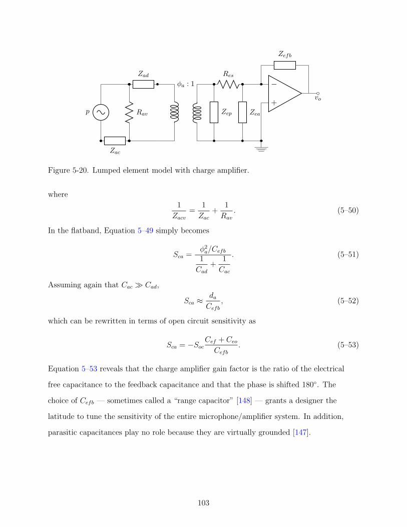
p Rav
Zac
Zad
φa : 1
Zep
Res
−
+
Zefb
vo
Zea
Figure 5-20. Lumped element model with charge amplifier.
where
1
Zacv
=1
Zac
+1
Rav
. (5–50)
In the flatband, Equation 5–49 simply becomes
Sca =φ2a/Cefb
1
Cad
+1
Cac
. (5–51)
Assuming again that Cac ≫ Cad,
Sca ≈daCefb
, (5–52)
which can be rewritten in terms of open circuit sensitivity as
Sca = −SocCef + Ceo
Cefb
. (5–53)
Equation 5–53 reveals that the charge amplifier gain factor is the ratio of the electrical
free capacitance to the feedback capacitance and that the phase is shifted 180. The
choice of Cefb — sometimes called a “range capacitor” [148] — grants a designer the
latitude to tune the sensitivity of the entire microphone/amplifier system. In addition,
parasitic capacitances play no role because they are virtually grounded [147].
103

5.3.3 Noise Models
In this section, noise models are developed for both the voltage and charge amplifier
circuit topologies. Ultimately, the goal of the noise models is to predict the output noise
PSD associated with the microphone/circuitry combination. The minimum detectable
pressure (MDP) is calculable from the result via Equation 2–11 or 2–12.
Noise has been previously discussed in Section 2.3.2. In the electrical domain, thermal
noise is proportional to the resistance and temperature. In terms of power spectral
density, the noise from an electrical resistor Re is given as [43]
SvRe
=4kBTRe (5–54)
or SiRe
=4kBT
Re
(5–55)
in units of [V2/Hz] and [A2/Hz], respectively. The superscripts v and i denote whether
SRedefines a source of voltage or current noise. Similarly, in the acoustic domain, the
noise contribution of a dissipative element in terms of power spectral density is
SpRa
=4kBTRa (5–56)
or SqRa
=4kBT
Ra
(5–57)
in units of [Pa2/Hz] and [m3/s/Hz], respectively. The superscripts p and q indicate
whether SRadefines a source of noise in terms of pressure or volume velocity, respectively.
To find the output noise of the circuit, all sources are first removed and noise sources,
defined by Equations 5–54 or 5–55 in the electrical domain and Equations 5–56 or 5–57
in the acoustic domain, are added at the site of each resistor/dissipator. Effort sources
(superscript v and p) are added in series with the resistors/dissipators, while flow sources
(i and q) are added in parallel [40, 42]. Under the assumption that the noise sources
are uncorrelated, the method of superposition of sources is used to find the total power
spectral density at the output due to all noise sources [40, 43]. The voltage and charge
amplifier circuit architectures are treated in turn in the following subsections.
104

5.3.3.1 Noise model with voltage amplifier
The noise model for the microphone/voltage amplifier combination is found in
Figure 5-21. The subscript of each source indicates the resistor with which it is associated.
The choice of using an effort source in series or a flow source in parallel with each
resistance is purely one of convenience. Additional noise sources are added for the
amplifier at its input [39] that represent the input-referred noise associated with internal
transistors and resistors [149]. These characteristics are known apriori based on the choice
of amplifier.
Zacv SqRav
SpRad Zad
φa : 1
Zep SiRep
SvRes Res
SiRea
−
+Svo
Zea
Sva
Sia
Figure 5-21. Noise model for the microphone with voltage amplifier circuitry.
Based on Figure 5-21, the output PSD [V2/Hz] is
Svo = Sv
o,Rav+ Sv
o,Rad+ Sv
o,Rep+ Sv
o,Res+ Sv
o,Rea+ Sv
o,a, (5–58)
i.e. the summation of the output-referred noise of each individual source. From circuit
analysis, the individual output noise contributions are
Svo,Rav
=
∣
∣
∣
∣
∣
∣
∣
∣
ZacvφA
(Zacv + Zad)
(
1
Zep
+1
Zea
+Res
ZepZea
)
+ φ2A
(
1 +Res
Zea
)
∣
∣
∣
∣
∣
∣
∣
∣
2
4kBT
Rav
, (5–59)
105

Svo,Rad+Ra,rad
=
∣
∣
∣
∣
∣
∣
∣
∣
φA
(Zacv + Zad)
(
1
Zep
+1
Zea
+Res
ZepZea
)
+ φ2A
(
1 +Res
Zea
)
∣
∣
∣
∣
∣
∣
∣
∣
2
4kBT (Rad + Rad,rad) ,
(5–60)
Svo,Rep
=
∣
∣
∣
∣
(Zeq −Res)Zea
Zeq + Zea
∣
∣
∣
∣
24kBT
Rep
, (5–61)
Svo,Res
=
∣
∣
∣
∣
Zea
Zeq + Zea
∣
∣
∣
∣
2
4kBTRes, (5–62)
Svo,Rea
=
∣
∣
∣
∣
ZeqZea
Zeq + Zea
∣
∣
∣
∣
24kBT
Rea
, (5–63)
and
Svo,amp =
∣
∣
∣
∣
ZeqZea
Zeq + Zea
∣
∣
∣
∣
2
Sia + Sv
a . (5–64)
Note in Equation 5–64 that the current noise Sia is multiplied by the parallel
combination of the microphone output impedance Zeq and Zea; low amplifier current
noise is therefore very important for high impedance devices. The piezoelectric MEMS
microphone, by virtue of its small expected capacitance, is just such a device.
Figure 5-22 shows a plot of output-referred noise contributions from each noise
source, with Rea neglected as established in Section 5.3.1. The same example geometry
used for validation in Section 5.2.5 is used here. Amplifier noise characteristics were
taken from the Linear Technologies LTC6240 amplifier, a low-noise amplifier with a
3 pF input capacitance and input-referred voltage and current noise floors of 7 nV/√
Hz
and 0.56 fA/√
Hz, respectively [44]. The noise associated with Rep dominates at low
frequencies until it gives way to amplifier current noise near 10 kHz. The voltage noise
contribution, in this case, is well below the current noise contribution. Meanwhile, the
combined acoustic noise contribution is completely insignificant compared to the electrical
noise.
The noise associated with Rep and the amplifier current noise are clearly dominant
in the example of Figure 5-22. However, noise characteristics of different amplifiers are
sufficiently variable that Sva also warrants continued inclusion in the noise model. Taking
106

10−1 100 101 102 103 104 105 10610−22
10−20
10−18
10−16
10−14
10−12
Frequency [Hz]
Noi
seP
SD
[V2/H
z] AcousticRep
Res
Sva
Sia
Total
Figure 5-22. Output-referred noise floor for the microphone with a voltage amplifier.
just the noise associated with Rep and the amplifier noise of the amplifier as dominant, the
noise floor of the microphone with the voltage amplifier architecture can be approximated
in the flatband as
Svo ≈
(
1
ωCet
)2(
Sia +
4kBT
Rep
)
+ Sva . (5–65)
Note that per Figure 5-22, there is some error associated with Equation 5–65 in the
current/voltage-noise dominant region, where the sum contribution of other noise sources
becomes significant. Making use of Equations 2–11 and 5–46, the minimum detectable
pressure is then
pmin ≈
√
√
√
√
√
√
∫ f2
f1
(
1jωCet
)2 (
Sia + 4kBT
Rep
)
+ Sva
(
Cef+Ceo
CetSoc
)2 df, (5–66)
which after making use of Equation 5–35, becomes
pmin ≈
√
√
√
√
∫ f2
f1
[
Sia + 4kBT
Rep
(ωda)2 +
SvaC
2et
d2a
]
df. (5–67)
Several important conclusions emerge from Equation 5–67. First, increasing da decreases
pmin. This follows naturally from knowledge of the fact that increasing sensitivity
decreases pmin, with Soc = −da/ (Cef + Ceo) from Equation 5–35. Following this logic,
the inverse relationship between Soc and Cef would also seem to suggest that a low
capacitance device would yield a lower pmin. However, Equation 5–67 shows that this is
107

Zacv SqRav
SpRad Zad
φa : 1
Zep SiRep
SvRes Res
−
+
Zefb
Svo
SiRefb
Zea
Sva
Sia
Figure 5-23. Noise model for the microphone with charge amplifier circuitry.
not always true; Cef plays no role in the noise floor when the dominant contributors are
Rep and Sia. When the dominant contributor is Sv
a , a low total capacitance Cet is desirable.
Finally, note that the first term rolls off as 1/ω2; this results in attenuation of noise due to
Rep at high frequencies, but current noise PSD in amplifiers often increases as ω2.
5.3.3.2 Noise model with charge amplifier
The noise model associated with the charge amplifier architecture is shown in
Figure 5-23. From this model, the total output noise PSD is thus
Svo = Sv
o,Rav+ Sv
o,Rad+Rad,rad+ Sv
o,Res+ Sv
o,Rep+ Sv
o,Refb+ Sv
o,amp, (5–68)
where the individual noise contributions are
Svo,Rav
=
∣
∣
∣
∣
∣
∣
φaZacvZefb
(Zad + Zacv)(
1 + Res
Zep
)
+ φ2aRes
∣
∣
∣
∣
∣
∣
2
4kBT
Rav
, (5–69)
Svo,Rad
=
∣
∣
∣
∣
∣
∣
Zefbφa
(Zad + Zacv)(
1 + Res
Zep
)
+ φ2aRes
∣
∣
∣
∣
∣
∣
2
4kBT (Rad + Rad,rad), (5–70)
Svo,Rep
=
∣
∣
∣
∣
Zefb (Zeq −Res)
Zeq
∣
∣
∣
∣
24kBT
Rep
, (5–71)
Svo,Res
=
∣
∣
∣
∣
Zefb
Zeq
∣
∣
∣
∣
2
4kBTRes, (5–72)
108

Svo,Refb
= |Zefb|24kBT
Refb
, (5–73)
and
Svo,amp =
∣
∣
∣
∣
1 +Zefb
Zeq ‖ Zea
∣
∣
∣
∣
2
Svamp + |Zefb|2 Si
amp, (5–74)
where recall Zeq is the electrical impedance of the microphone, introduced in Section 5.2.4.
Clearly, one important conclusion from the noise model is that Zefb figures prominently
in each of Equations 5–68 to 5–74. In addition, only the voltage noise is impacted by the
presence of parasitics.
Individual noise sources associated with the microphone and charge amplifier
architecture are shown in Figure 5-24. The example amplifier was taken as the Texas
Instruments OPA129, with an assumed input capacitance of 3 pF and manufacturer-supplied
input-referred voltage and current noise floors of 15 nV/√
Hz and 0.1 fA/√
Hz, respectively.
The feedback impedances were chosen as Cefb = Cef + Ceo ≈ 8 pF (unity gain) and
Rfb = 2 GΩ (cut-off at 10 Hz). With this configuration, the dominant noise source
is again seen to be Rep at low frequencies, while amplifier voltage noise dominates
beyond the corner frequency at approximately 10 kHz. The feedback resistance Refb
also shows potential of contributing if chosen as a lower value. Again, the acoustic noise is
inconsequential.
10−1 100 101 102 103 104 105 106
10−20
10−18
10−16
10−14
10−12
10−10
Frequency [Hz]
Noi
seP
SD
[V2/H
z] AcousticRep
Res
Refb
Sva
Sia
Total
Figure 5-24. Output-referred noise floor for the microphone with charge amplifier.
Much latitude exists in the selection of Refb, and the amplifier, so noise associated
with each of them, together with the ever-dominant noise source Rep, are included in
109

simplifications to the overall noise floor. In the flatband, Svo simplifies to
Svo ≈
(
1 +Cet
Cefb
)2
Sva +
(
1
ωCefb
)2 [
Sia + 4kBT
(
1
Rep
+1
Refb
)]
. (5–75)
Note from this equation that the resistor noise can be viewed as originating from an
equivalent resistor, Rep ‖ Refb. The minimum detectable pressure then follows, after some
simplification, as
pmin ≈
√
√
√
√
√
∫ f2
f1
Sia + 4kBT
(
1Rep
+ 1Refb
)
(ωda)2 +
(Cefb + Cet)2 Sv
a
d2a
df. (5–76)
Again, increasing da decreases pmin. Although parasitics do not impact the sensitivity in
the charge amplifier case, Equation 5–76 shows that they still tend to increase pmin when
Sva is important. The term containing Si
a and Rep ‖ Refb rolls-off as 1/ω2, but again, Sia
tends to increase as ω2.
5.3.4 Selection
Table 5-2 contains a summary of the two main performance characteristics of the
microphone and interface circuitry addressed in Sections 5.3.1 to 5.3.3: sensitivity and
minimum detectable pressure. In the voltage amplifier case, the theoretical open-circuit
sensitivity is always attenuated by parasitic capacitances, while in the charge amplifier
case the sensitivity is not affected by parasitics. In the charge amplifier case, a designer
has latitude to attenuate or gain the sensitivity via the choice of feedback capacitor as
well.
Table 5-2. Comparison of voltage and charge amplifier topologies for use with apiezoelectric microphone.
Sensitivity (S) Minimum detectable pressure (pmin)
Voltage AmplifierCef
CetSoc
√
∫ f2f1
[
Sia+
4kBT
Rep
(ωda)2 +
SvaC
2et
d2a
]
df
Charge Amplifier − Cef
CefbSoc
√
√
√
√
∫ f2f1
[
Sia+4kBT
(
1Rep
+ 1Refb
)
(ωda)2 +
(Cefb+Cet)2Sva
d2a
]
df
110

Comparing the minimum detectable pressures for the two amplifier configurations
term-by-term, the amplifier current noise contribution is seen to be the same for
both, assuming both amplifiers have equivalent current noise characteristics. At best,
the additional noise from the bias resistor in the charge amp case can be mitigated
by choosing Refb ≫ Rep. The final voltage noise term is where the two are truly
differentiated; assuming equivalent amplifier voltage noise in both configurations, the
total contribution to the minimum detectable pressure from the charge amp circuit will
always be higher due to the appearance of Cefb in the numerator.
For a microphone with very high gain (Cefb ≪ Cef ), the added voltage noise of
the charge amp can be minimized, but Cefb cannot be decreased without bound. The
feedback impedance introduces an additional cut-on frequency, fc = 1/2πRefbCefb.
As Cefb decreases, fc increases and the bandwidth of the microphone can be reduced.
Compensating with a larger Refb is not always straightforward [149]. There is thus a
delicate balance between gain, cut-off, and noise in the charge amplifier architecture.
The primary advantage of charge amplifiers is that the microphone sensitivity is not
dependent on parasitic capacitance. Parasitic capacitance is introduced, for example, by
wire bonds, traces, or cables between the sensor and the interface electronics. Charge
amplifiers, then, are popular because they can be located remotely from the actual sensor;
changes in cable or trace lengths (and the associated change in parasitic capacitance) do
not affect the sensitivity or require subsequent recalibration [146]. Meanwhile, a voltage
amplifier must be located close to the sensor to minimize the attenuation in sensitivity.
Deploying thousands of microphones on the exterior of an aircraft demands the
utmost in simplicity. Collocating the microphone and signal conditioning circuitry in
a single package yields a compact and complete sensor system that can be connected
directly to a DAQ without regard for additional circuitry. Even in the laboratory setting,
the amplifier may be located in close proximity to the microphone. The voltage amplifier
111

is the appropriate choice for such a case. In addition, the relative simplicity of the voltage
amplifier configuration, with its low part count and fewer trade-offs to assess, is attractive.
As a result, the voltage amplifier was chosen as the interface circuit for this study.
The majority of measurements presented in Chapter 8 are specific to the voltage amplifier
case. Measurements for one microphone instrumented with a charge amplifier — for
comparison of sensitivity and to estimate parasitic capacitances — are presented in
Section 8.2.4.3.
5.4 Summary
In this chapter, models for the performance of a piezoelectric microphone have been
developed, including a lumped element model, a diaphragm mechanical model, and noise
models. In the next chapter, the developed models are used in a structural optimization
formulation to determine the geometry that delivers optimal microphone performance.
112

CHAPTER 6OPTIMIZATION
This chapter is concerned with choosing microphone dimensions within constraints
such that the “best” performance is obtained; this process is known as optimization [150].
The lumped element model developed in Chapter 5 provides predictions of microphone
performance and aids intuitive understanding of design tradeoffs. The intuitive selection
of a “best” design in the presence of many design variables and constraints, however, is
difficult. The low computational cost associated with the lumped element model makes it
ideally suited for integration with an optimization algorithm that systematically identifies
the “best” design. In this chapter, an overview of the design optimization problem is first
given, including discussion of geometric dimensions available for selection and performance
characteristics to be extremized. Next, the optimization problem is formally defined and
the approach for solving it is outlined. Finally, the results of the optimization process are
discussed.
6.1 Design Overview
6.1.1 Design Variables
The use of a commercial foundry process to fabricate devices leverages significant
engineering investment but also places constraints on available geometries. With a
compatible geometry established, an important early step in the design process is
thus identification of design variables. Figure 6-1 shows a cross-sectional view of the
piezoelectric microphone — as dictated by the film bulk acoustic resonator (FBAR)
variant process discussed at length in Section 4.2 — with important dimensions labeled.
Free dimensions may serve as design variables for the structural optimization
problem, while fixed dimensions, denoted in Figure 6-1 with a symbol, may not. The
cavity depth dc is set by the wafer thickness. The diaphragm overlap ∆a0 and undercut
∆ac are standard features of the FBAR-variant fabrication process, as is the passivation
113

oa∆
1a
`
rz
a∆
cd caca∆
hstruct
he,bot
he,top
hp
hpass
Figure 6-1. Cross-section of the piezoelectric microphone with notable dimensions to beconsidered; those denoted with are fixed by the fabrication process.
layer thickness hpass. The values associated with these fixed dimensions and others not
shown in Figure 6-1 are collected in Table 6-1.
Table 6-1. Microphone dimensions fixed by the fabrication process.
Dimension Value µm Description
∆ao 3 Width of diaphragm overhang∆ac 35 Width of diaphragm undercuthpass 0.14 Thickness of passivation layerdc 500 Cavity depthLv 50 Vent lengthhv 2 Vent heightbv 25 Vent width
Meanwhile, several “free” dimensions remain whose values may be selected within
bounds established by the fabrication process, including the film thicknesses and
diaphragm radii. There are thus 7 design variables in total: the inner radius, a1; the
width of the annular piezoelectric film stack, ∆a; and the film thicknesses associated
with the top electrode, piezoelectric, bottom electrode, and structure layers, he,top, hp,
he,bot, and hstruct, respectively. The dimension ∆a is used in place of a2 to specify the
outer radius of the diaphragm (i.e. a2 = a1 + ∆a) because it makes selection of the
two dimensions independent; using a2 as a design variable requires enforcement of the
condition a2 ≥ a1. Note also that the cavity radius ac is set by selection of the diaphragm
114
radii, as from Figure 6-1,
ac = a1 + ∆a− ∆ac. (6–1)
6.1.2 Objective
The extremization of a performance measure subject to certain constraints is the
purpose of optimization. Determining an optimal design first requires the appropriate
measure(s) of what constitutes “best” performance — called the objective function(s) —
to be identified. The concept of the operational “space” in the frequency and pressure
domains was introduced in Chapter 2 in terms of the microphone bandwidth and dynamic
range. Maximizing this “space” subject to the needs of the particular application is one
way of approaching microphone design. At minimum, a MEMS piezoelectric microphone
design must be identified that precisely meets all sponsor performance specifications
(Section 1.2). The first question to be answered in the optimization process is thus
whether or not the specified performance is achievable within the design space established
by the fabrication process, base geometry, material choices, etc. Beyond that, the
questions to be answered are whether performance can be improved beyond the given
specifications and what additional performance gains are most beneficial.
Microphone bandwidth exceeding the audio range (20 Hz–20 kHz) is not beneficial
in any full-scale aeroacoustic measurement application, including the fuselage array
application. Although additional bandwidth could enable the microphone to be leveraged
to model-scale applications, examining the design trade-offs for full-scale and model-scale
measurements was not a focus of this study. Exceeding the specified dynamic range,
meanwhile, has an obvious benefit in the target fuselage array application: lowering MDP
improves measurement resolution.1 In addition to improving performance in the target
application, exceeding specifications on MDP could enable the microphone to be leveraged
1 Lowering MDP improves measurement resolution up to the limits of the associated data acquisitionsystem.
115

directly to other full-scale applications, such as flyover arrays. Minimum detectable signal
in general has been established as a key comparative figure of merit for sensors [151, 152].
Exceeding the specified maximum pressure level of 172 dB — the highest pressure
level of practical interest in aeroacoustic measurements of aircraft — does not yield similar
benefits. However, the design trade-off between the specified PMAX and obtainable
MDP is of fundamental importance for the present design effort; in the event that
specified performance for these two quantities is not achievable, knowledge of the
trade-offs drives specification revisions or design space modifications. To study the
trade-offs, extremization of both MDP and PMAX were taken as optimization objectives.
The resulting optimization formulation is known as a multicriteria or multiobjective
optimization [150, 153].
Due to competition among objective functions, multiobjective optimization problems
are characterized by the non-existence of a unique solution. For example, any number of
minimum values for MDP may be achievable given sacrifices in the maximum attainable
value of PMAX. Without a decision-maker to express preference, a set of mathematically
equivalent solutions known as the Pareto-optimal set emerges [153]. A solution is said
to be Pareto optimal if the selection of any other set of design variable values results in
all objective functions remaining unchanged or at least one getting “worse” [150]. An
example of a set of Pareto-optimal solutions — often called a Pareto front — is shown in
Figure 6-2, where maximization of PMAX and minimization of MDP are taken as the two
objectives. In this figure, designs A, B, and C are Pareto-optimal but D is not. Similarly,
Papila et al. (2006) [152] found Pareto-optimal solutions associated with simultaneous
maximization of sensitivity and minimization of electronic noise for a piezoresistive
microphone.
Algorithms exist for finding the set of Pareto-optimal solutions directly [153, 154].
However, more commonly-available single-objective optimization software tools may be
used to find the Pareto front via solution of a sequence of constrained single-objective
116

PMAX
MDP
Feasible
Region
Pareto frontC
B
A
D
Figure 6-2. Pareto front example.
problems. Using this approach, one objective is extremized while the other is treated as a
constraint [150]. The constraint is varied over a range of values until the Pareto front is
resolved. This is known as the ε-constraint method [153] and is used in the optimization
approach for the piezoelectric microphone, discussed further in Section 6.3.
6.2 Formulation
In this section, the optimization problem is formalized. The objective function, design
variables, bounds, and constraints are all defined and discussed.
The objective of the optimization is
minX
fobj (X) = MDP, (6–2)
where the narrow-band definition of MDP is selected for this study, i.e. MDP evaluated
for a 1 Hz bin width centered at 1 kHz. The associated design variables are
X = a1,∆a, hetop, hp, hebot, hstruct (6–3)
subject to bounds (or side constraints)
LB ≤ X ≤ UB. (6–4)
Specific values of LB and UB set by the FBAR-variant process are found in Table 6-2.
Geometrical, fabrication, modeling, and performance constraints are all present in the
optimization problem. Many fabrication constraints are reflected in the bounds placed on
117

Table 6-2. Design variable bounds.
X LB [µm] UB [µm]
a1 5 600∆a 5 600he,top 0.1 0.2hp 0.3 1he,bot 0.2 0.6hstruct 1 2
each design variable, while other constraints are dependent on multiple design variables.
These are classified as linear or nonlinear constraints depending on their functional
dependence on the design variables. There are 3 linear constraints and 1 nonlinear
constraint. The constraints are:
1. The microphone diaphragm must be sufficiently thin such that the Kirchhoff platetheory used in the diaphragm mechanical model remains applicable. The thinnessof the diaphragm was quantified via the aspect ratio, AR (a/h), for both the inner(0 ≤ r ≤ a1) and outer (a1 ≤ r ≤ a1 + ∆a) regions of the diaphragm. The constraintsare
a1 ≥ AR (hpass + hstruct) (6–5)
and∆a ≥ AR (hpass + he,top + hp + he,bot + hstruct) . (6–6)
AR was chosen to be 10 [121].2
2. A fabrication constraint on the maximum radius was more restrictive than thesensing element size requirement of Section 1.2:
a1 + ∆a ≤ 600µm. (6–7)
3. A fabrication constraint was also placed on the minimum radius:
a1 + ∆a ≥ 250µm. (6–8)
4. The sole nonlinear constraint was on the maximum pressure; the pressure at whichtotal harmonic distortion (THD) reached 3% was required to meet or exceed 172 dB
2 A plate is generally defined as “a structural element with planform dimensions that are large com-pared to its thickness” [121]. The specific minimum relationship between these dimensions is not preciselyprescribed, though aspect ratios of 10–20 are commonly cited [37, 121].
118

per the design objectives in Section 1.2. With a computationally efficient predictionmethod for total harmonic distortion of the microphone unavailable, a constraint onstatic nonlinearity of the diaphragm was used instead. For the maximum pressurepmax, the total center deflection of the diaphragm predicted using the linear andnonlinear models (see Appendix A) was restricted to be ≤ 3 %, i.e.
∣
∣
∣
∣
w0,l − w0,nl
w0,nl
∣
∣
∣
∣
p=pmax
≤ 0.03, (6–9)
where subscript l indicates the linear model and subscript nl indicates thenonlinear model. Although the quality of this measure of nonlinearity as a predictionfor THD was unknown, intuition suggested that THD would trend similarly.Uncertainty in the constraint was partially addressed in the optimization approach,discussed in Section 6.3.
Note that no constraints on bandwidth were defined in order to meet the f±2 dB
targets set out in Chapter 1. Microphones designed for high pmax are necessarily stiff with
high resonant frequencies, so it was not anticipated that satisfying f+2dB ≥ 20 kHz would
be an issue. No constraint was placed on f−2 dB (i.e. f−2 dB ≤ 20 Hz) out of concern that
unreliable predictions for this quantity, dominated by either the RepCeb or RavCac break
frequencies, would drive the optimization. At the time of the optimization, predictions
of Rep were based on impedance measurements of early prototype devices, but there was
little confidence in the measurement quality. Meanwhile, the Rav prediction was reliant
on assumptions almost certain to not be satisfied, for example fully-developed flow in
the vent channel. With the vent geometry set, enforcing f−2 dB ≥ 20 Hz would lead the
optimization algorithm to increase the RavCac product via enlarging the cavity radius,
which by Equation 6–1 would lead to bigger diaphragms with lower stiffness and lower
achievable pmax. Despite the lack of bandwidth constraints, the bandwidth of the optimal
sensor was assessed for adherence to the design requirements following the optimization.
6.3 Approach
The optimization problem defined in Section 6.2 is a single-objective problem with
both linear and nonlinear constraints. It was solved using the fmincon function in
MATLAB, which is applicable to nonlinear constrained optimization problems. This
119
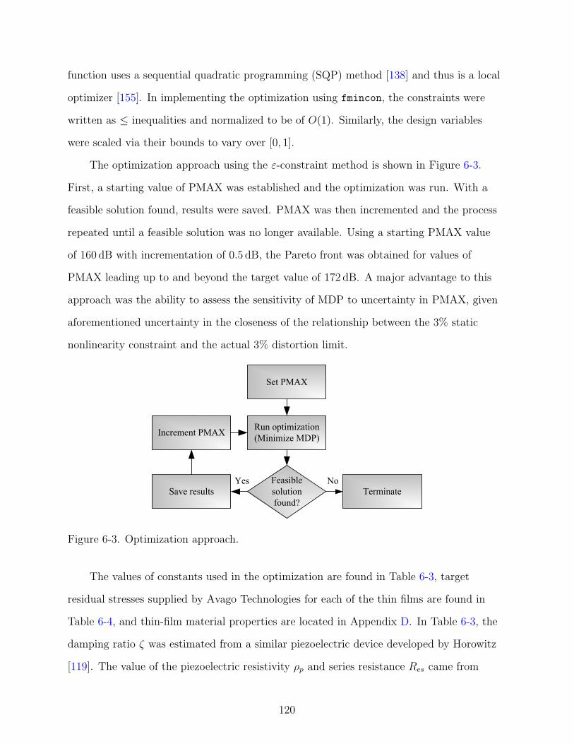
function uses a sequential quadratic programming (SQP) method [138] and thus is a local
optimizer [155]. In implementing the optimization using fmincon, the constraints were
written as ≤ inequalities and normalized to be of O(1). Similarly, the design variables
were scaled via their bounds to vary over [0, 1].
The optimization approach using the ε-constraint method is shown in Figure 6-3.
First, a starting value of PMAX was established and the optimization was run. With a
feasible solution found, results were saved. PMAX was then incremented and the process
repeated until a feasible solution was no longer available. Using a starting PMAX value
of 160 dB with incrementation of 0.5 dB, the Pareto front was obtained for values of
PMAX leading up to and beyond the target value of 172 dB. A major advantage to this
approach was the ability to assess the sensitivity of MDP to uncertainty in PMAX, given
aforementioned uncertainty in the closeness of the relationship between the 3% static
nonlinearity constraint and the actual 3% distortion limit.
Set PMAX
Run optimization
(Minimize MDP)
Feasible
solution
found?
Save results
Increment PMAX
Yes
Terminate
No
Figure 6-3. Optimization approach.
The values of constants used in the optimization are found in Table 6-3, target
residual stresses supplied by Avago Technologies for each of the thin films are found in
Table 6-4, and thin-film material properties are located in Appendix D. In Table 6-3, the
damping ratio ζ was estimated from a similar piezoelectric device developed by Horowitz
[119]. The value of the piezoelectric resistivity ρp and series resistance Res came from
120

mean impedance measurements of several prototype microphones. The bias resistor Rea
was disregarded because early experiments showed that it was unnecessary for stable
operation of the piezoelectric microphone with voltage amplifier. The amplifier input
capacitance Cea and noise characteristics Sva and Si
a were all obtained from the datasheet
for the chosen amplifier, the LTC6240 [44]. The residual stress characteristics of the
thin-film stack found in Table 6-4 emerged from significant process development efforts
at Avago Technologies, and the information was leveraged in the optimization to enhance
model predictions.
Table 6-3. Constant values used in the optimization.
Parameter Value
ζ [119] 0.03Res 4.14 kΩρp 22.8 MΩ mRea ∞Cea [44] 3 pF
Sva [44]
(
7950Hzf
+ 49)
nV2/Hz†
Sia [44]
(
1.27× 10⁻⁶
Hz2f 2 − 4.85× 10⁻⁵
Hzf + 0.354
)
fA2/Hz†
† Curve fit to data in [44]
Table 6-4. Target thin-film residual stresses.
Layer Residual Stress [MPa]
Passivation −50Top Electrode −150Piezoelectric 0Bottom Electrode −100Structural 55
6.4 Results and Discussion
The optimization using the ε-constraint method yielded the Pareto front shown in
Figure 6-4. In order to increase the effective piezoelectric coefficient, the general trend of
the optimization algorithm is to increase the diaphragm outer radius (a1 + ∆a) as much
121

as possible (while making minor changes to the percentage piezoelectric coverage, ∆a/a1)
until the nonlinearity constraint becomes active. For PMAX ≤ 165 dB, the maximum
radius constraint is activated and the optimization algorithm loses its primary method
of reducing MDP. As a result, the attainable minimum values of MDP are seen to be
less sensitive to the specified value of PMAX in this regime. Meanwhile, the relationship
between PMAX and MDP is seemingly linear for PMAX ≥ 165 dB, indicating a power
law relationship between pmax and pmin. Note that no feasible solutions were found for
PMAX>174 dB, beyond which the minimum diaphragm radius constraint activates.
160 162 164 166 168 170 172 17430
35
40
45
50
GF
ED
CB
AFeasible region
PMAX [dB]
MD
P[d
B]
Figure 6-4. Pareto front associated with minimization of MDP and maximization ofPMAX. The shaded region indicates the target design space.
Designs selected for fabrication are indicated with labels A–G in Figure 6-4. Designs
A–C satisfied the design criteria — with PMAX≥172 dB and MDP≤48.5 dB — and were
thus obvious choices. With the possibility that the static nonlinearity constraint was a
conservative prediction for total harmonic distortion, designs D–G, which did not reach
the PMAX=172 dB target, were also selected in order to provide the possibility of meeting
the PMAX target with superior MDP compared to designs A–C. All of the selected
designs featured the same optimal film thicknesses and thus were able to be fabricated
together on a single wafer, eliminating the need for secondary optimization to constrain
the designs to a single set of film thicknesses. When this additional step is required,
performance is inevitably sacrificed for a subset of designs.
122
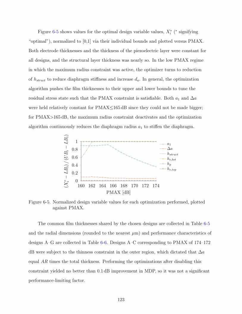
Figure 6-5 shows values for the optimal design variable values, X∗i (∗ signifying
“optimal”), normalized to [0,1] via their individual bounds and plotted versus PMAX.
Both electrode thicknesses and the thickness of the piezoelectric layer were constant for
all designs, and the structural layer thickness was nearly so. In the low PMAX regime
in which the maximum radius constraint was active, the optimizer turns to reduction
of hstruct to reduce diaphragm stiffness and increase da. In general, the optimization
algorithm pushes the film thicknesses to their upper and lower bounds to tune the
residual stress state such that the PMAX constraint is satisfiable. Both a1 and ∆a
were held relatively constant for PMAX≤165 dB since they could not be made bigger;
for PMAX>165 dB, the maximum radius constraint deactivates and the optimization
algorithm continuously reduces the diaphragm radius a1 to stiffen the diaphragm.
160 162 164 166 168 170 172 1740
0.2
0.4
0.6
0.8
1
PMAX [dB]
(X∗ i−
LB
i)/
(UB
i−LB
i)
a1∆a
hstruct
he,bot
hp
he,top
Figure 6-5. Normalized design variable values for each optimization performed, plottedagainst PMAX.
The common film thicknesses shared by the chosen designs are collected in Table 6-5
and the radial dimensions (rounded to the nearest µm) and performance characteristics of
designs A–G are collected in Table 6-6. Designs A–C corresponding to PMAX of 174–172
dB were subject to the thinness constraint in the outer region, which dictated that ∆a
equal AR times the total thickness. Performing the optimizations after disabling this
constraint yielded no better than 0.1 dB improvement in MDP, so it was not a significant
performance-limiting factor.
123

Table 6-5. Optimal layer thicknesses.
Symbol Value [µm]
hpass 0.14†
he,top 0.1‡
hp 1§
he,bot 0.6§
hstruct 2§
† Fixed ‡ At lower bound § At upper bound
Table 6-6. Optimization results.
Design
A B C D E F G
PMAX [dB] 174 173 172 171 170 169 168
a1[µm]† 219 245 274 306 338 373 412∆a [µm]† 38‡ 38‡ 38‡ 39 40 41 43MDP [dB] 48.1 46.5 45.0 43.3 41.8 40.3 38.7f−2 dB [Hz] 64 66 68 71 73 75 78f+2dB [kHz] 129 113 100 89 80 72 65Soc [dB re 1 V/Pa] −88.8 −87.7 −86.6 −85.5 −84.5 −83.5 −82.5Sva [dB re 1 V/Pa] −92.4 −91.0 −89.6 −88.2 −87.0 −85.8 −84.5
† Rounded to the nearest µm ‡ AR constraint active
With no constraint placed on f−2 dB, this metric did exceed 20 Hz for all of the
selected designs. Further investigation revealed that it was dominated by Rep rather
than Rav. Only about 0.25 % of the total desired bandwidth did not meet specifications;
given aforementioned uncertainty in Rep, it was decided to go ahead with fabrication.
Meanwhile, f+2dB was well above 20 kHz as expected, and designs A–D were predicted to
possess sufficient bandwidth for potential leveraging of the microphones to model-scale
applications.
Analyzing the sensitivity of MDP and PMAX to perturbations in design variables or
other inputs yields additional insight into the results. Figure 6-6 shows how perturbing
124

optimal dimensions associated with design C by ±10 % affected MDP.3 The most
important design variables were a1 and ∆a, for which a 10 % variation yielded approximately
1–1.5 dB change in MDP.
0.9 0.95 1 1.05 1.1
−1
0
1
Xi/X∗i
MD
P-M
DP*
[dB
] a1∆a
hstruct
he,bot
hp
he,top
Figure 6-6. Sensitivity of MDP to ±10 % perturbations in the design variables for DesignC. The x and y axes are referenced to the values of the design variables andMDP, respectively, at the optimal solution.
Similarly, Figure 6-7 shows the sensitivity of PMAX to perturbations in the optimal
dimensions for design C.3 PMAX is seen to be more sensitive to the design variables,
most notably hstruct, a1, and ∆a in that order. PMAX is particularly sensitive to hstruct
because the thick structural layer, with its tensile stress, plays a major role in setting the
overall state of in-plane stress. Comparing Figures 6-6 and 6-7, it is seen that increasing
hstruct 10 % beyond its optimal value yields nearly a 1 dB improvement in PMAX with
only a 0.3 dB penalty in MDP. The calculus of modifying any of the other design variables
is not as attractive, indicating that the 2µm upper bound on hstruct is a significant
performance-inhibitor.
Microphone performance metrics are also sensitive to uncertainty in model inputs,
most notably those for in-plane stress. To study this sensitivity, a Monte Carlo simulation
was performed in which the stresses were perturbed about their target values using
3 Given the linear nature of Figure 6-6 and Figure 6-7, the sensitivities also could have been character-ized directly via logarithmic derivatives [150, 152].
125
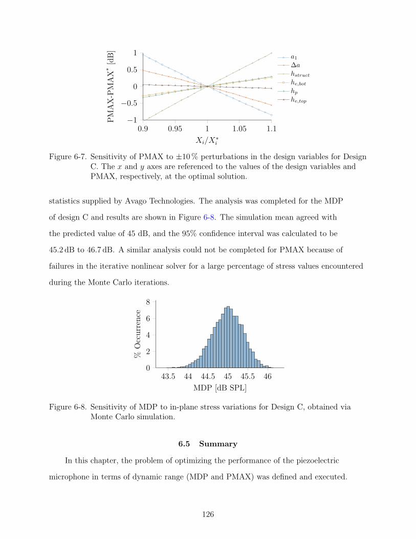
0.9 0.95 1 1.05 1.1−1
−0.5
0
0.5
1
Xi/X∗i
PM
AX
-PM
AX
*[d
B]
a1∆a
hstruct
he,bot
hp
he,top
Figure 6-7. Sensitivity of PMAX to ±10 % perturbations in the design variables for DesignC. The x and y axes are referenced to the values of the design variables andPMAX, respectively, at the optimal solution.
statistics supplied by Avago Technologies. The analysis was completed for the MDP
of design C and results are shown in Figure 6-8. The simulation mean agreed with
the predicted value of 45 dB, and the 95% confidence interval was calculated to be
45.2 dB to 46.7 dB. A similar analysis could not be completed for PMAX because of
failures in the iterative nonlinear solver for a large percentage of stress values encountered
during the Monte Carlo iterations.
43.5 44 44.5 45 45.5 460
2
4
6
8
MDP [dB SPL]
%O
ccu
rren
ce
Figure 6-8. Sensitivity of MDP to in-plane stress variations for Design C, obtained viaMonte Carlo simulation.
6.5 Summary
In this chapter, the problem of optimizing the performance of the piezoelectric
microphone in terms of dynamic range (MDP and PMAX) was defined and executed.
126

Seven designs (A–G) were selected for fabrication, with 3 (A–C) meeting or exceeding
requirements on MDP and PMAX. Optimization trends and the sensitivity of both MDP
and PMAX to perturbations in the design variables were also discussed. The next chapter
addresses the realization of these microphone designs and packaging of the microphones
for experimental characterization.
127

CHAPTER 7REALIZATION AND PACKAGING
This chapter focuses on the realization of individually packaged piezoelectric
microphones, bridging the gap between the theoretical designs of Chapter 6 and
experimental characterization in Chapter 8. First, the results of the fabrication process
performed at Avago Technologies are discussed. Next, the method developed to separate
the microphone die is explained. Finally, the laboratory test package developed specifically
for the piezoelectric microphones is described.
7.1 Realization
This section focuses on realization of the piezoelectric microphones. The as-fabricated
microphone geometries are explicitly given and fabrication results are discussed.
7.1.1 Geometry
Optimal piezoelectric microphone geometries were found in Chapter 6. From those
results, seven different geometries covering a swath of design space were submitted for
fabrication. With expected uncertainties in model predictions and film stress targeting,
fabrication of multiple microphone geometries was judged to provide the most probable,
cost-sensitive, and schedule-effective path to meeting performance specifications. The
diaphragm dimensions for designs labeled A-G (in order of increasing diameter) are found
in Table 7-1 and their common film thickness and stress targets are in Table 7-2. After
the fabrication lot was started, Avago suggested based on recent experience that the top
electrode thickness he,top be changed from 0.1µm to 0.15µm. The models confirmed that
sensitivity of MDP and PMAX to this design variable was low (recall Figures 6-6 and 6-7).
It was thus decided to accept the change in he,top, which is reflected in Table 7-2.
7.1.2 Fabrication Results
Fabrication was performed at Avago Technologies using a variant of their film bulk
acoustic resonator (FBAR) process [82, 83, 105]. The fabrication process was addressed
128

Table 7-1. Design dimensions.
Design a1 [µm] ∆a [µm] a2 [µm]
A 219 38 257B 245 38 283C 274 38 312D 306 39 345E 338 40 378F 373 41 414G 412 43 455
Table 7-2. Film properties.
Layer Thickness [µm] Stress Target [MPa]
Structural Layer 2 55Bottom Mo 0.6 0AlN 1 0Top Mo 0.15 -150Passivation 0.14 -50
in Section 4.2. A photograph of a completed wafer is found in Figure 7-1. In all, Avago
Technologies delivered eight 6” wafers with microphone die 2 mm on a side.
Avago Technologies provided the wafers with film stress information. After each film
deposition, wafer curvature was measured with a Tencor Flexus FLX 5400 and the film
stress was estimated from these measurements using Stoney’s Formula [107, 108, 156],
σ =Est
2s
6tf (1 − ν)
(
1
R− 1
R0
)
, (7–1)
where σ is the film stress, Es, ν, and ts are the Young’s Modulus, Poisson’s Ratio, and
thickness of the substrate, respectively, tf is the film thickness, and R0 and R are the
radii of curvature before and after film deposition, respectively. Stoney’s Formula is
a wafer-level stress estimation that relies on a number of assumptions that may be
only approximately valid, such as transverse isotropy of the substrate, uniform film
thickness, and homogeneous stress, among others [107]. Despite the caveats, these
estimates represented the best-available film stress information.
129
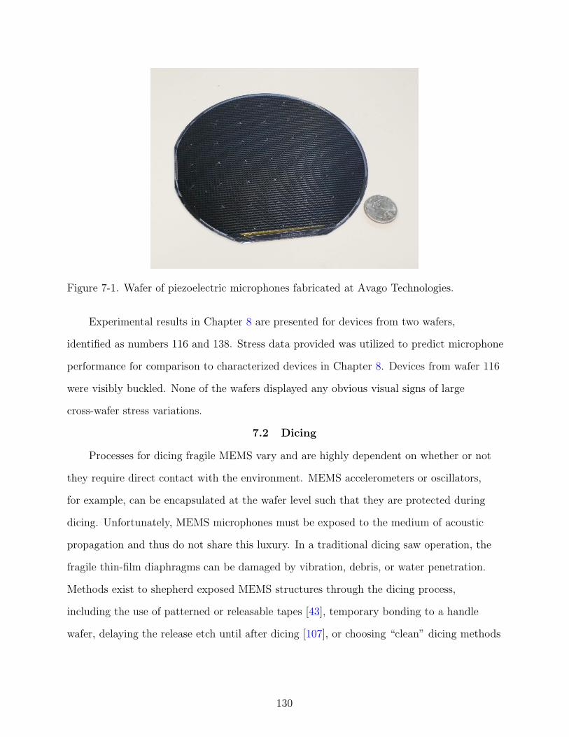
Figure 7-1. Wafer of piezoelectric microphones fabricated at Avago Technologies.
Experimental results in Chapter 8 are presented for devices from two wafers,
identified as numbers 116 and 138. Stress data provided was utilized to predict microphone
performance for comparison to characterized devices in Chapter 8. Devices from wafer 116
were visibly buckled. None of the wafers displayed any obvious visual signs of large
cross-wafer stress variations.
7.2 Dicing
Processes for dicing fragile MEMS vary and are highly dependent on whether or not
they require direct contact with the environment. MEMS accelerometers or oscillators,
for example, can be encapsulated at the wafer level such that they are protected during
dicing. Unfortunately, MEMS microphones must be exposed to the medium of acoustic
propagation and thus do not share this luxury. In a traditional dicing saw operation, the
fragile thin-film diaphragms can be damaged by vibration, debris, or water penetration.
Methods exist to shepherd exposed MEMS structures through the dicing process,
including the use of patterned or releasable tapes [43], temporary bonding to a handle
wafer, delaying the release etch until after dicing [107], or choosing “clean” dicing methods
130

such as scribe/break [157] or laser cutting [158]. In this section, an in-house process for
dicing the microphone die using protective tape is described.
7.2.1 Dicing Process
The most advanced dicing option available at UF’s Nanoscale Research Facility is an
ADT 7100 Dicing Saw, which uses a physical blade and associated jet of deionized water
for cooling and debris removal. Figure 7-2 shows the blade dicing a wafer sample, with
the water jet impinging on the sample opposite the cutting direction. Protection of the
mic diaphragms is thus a necessity, but any substance used to protect the devices must be
easily removable post-dice without damaging the diaphragms. Protective tapes, such as
UV tape or thermal release tape are sound options. In the process described herein, Nitto
Denko REVALPHA thermal release tape (No. 3198M) was used for diaphragm protection.
This tape is double-sided, with a regular adhesive on one side and a temperature sensitive
adhesive on the other. At 120 C, the temperature sensitive adhesive releases completely.
Cut direction
XXXXXXXXXz
Water jet)
Leading edgePPPPPq
Trailing edge
XXXXXXXXXXy
Sample
JJJJ
Nickel resin blade
Figure 7-2. Dicing blade and sample orientation.
Early experiments on prototype 3 mm die using solely thermal release tape to protect
the diaphragms proved extremely successful, with nearly 100% yield. However, the smaller
2 mm die did not provide sufficient area for reliable tape adhesion, resulting in peeling
during dicing and significant die loss. As a result, an additional protective polyethylene
tape (commonly used for surface protection in the construction industry) was used in a
131

more elaborate process. The entire process was performed on an ADT 7100 Dicing Saw
equipped with nickel resin blades.
The method for using the protective tapes during the dicing process is depicted in
Figure 7-3. To reduce the time and risk of each dice run, wafer sections (or samples) were
individually diced. They were obtained via diamond scribing and breaking, with typical
pieces containing 3-6 reticles. The backside of the sample was first affixed to medium tack
dice tape, used for mounting the sample in the dicing machine. Next, the thermal release
tape was applied to the front side (diaphragm side) of the sample, with only the protective
backing associated with the thermal release adhesive removed. The thermal release tape
was applied even with the sample edges on the cut entry edges, but extending off the
sample up to 15 mm on the trailing edges (as shown in Figure 7-3A) to provide additional
adhesion and protection from the dicing machine’s water jet. Next, without removing the
remaining plastic backing on the backside of the thermal release tape, the polyethylene
tape was applied over the complete sample to provide additional protection, as shown in
Figure 7-3A. The sample was then diced in the first direction, with cuts extending slightly
off the leading and trailing edges of the sample. The complete tape layup for this step
is shown in Figure 7-3B, and the tape thicknesses, which are important for setting the
cut depth, are collected in Table 7-3. Important dicing machine settings are collected in
Table 7-4.
Table 7-3. Tape and substrate thicknesses.
Material Thickness [µm]
Substrate 500Dice tape 130Thermal release tape (without laminates) 160Thermal release tape laminate 75Polyethylene tape 70
With cuts completed in a single direction, the sample was then removed from the
dicing machine and the polyethylene tape was smoothly peeled away from the thermal
132

)
Wafersample
)Thermalrelease tape
)Polyethylenetape
XXXXXXXXz
Dicepattern
6
1st CutDirection
2nd CutDirection
A
AAAU
Polyethylenetape A
AAU
Tapebacking
+
Thermalrelease tape
+
Wafersample
+
Dicetape
B
AAAU
Polyethylenetape B
BBN
Thermalrelease tape
Wafersample
Dicetape
C
Figure 7-3. Dicing process for MEMS piezoelectric microphone die. A) Aerial view of diceprocess taping technique. B) Cross-sectional view of taping technique for firstdirection dice cuts. C) Cross-sectional view of taping technique for seconddirection dice cuts.
Table 7-4. Dicer settings.
Parameter Setting
Spindle speed 30 krpmEntry speed 0.5 mm/sCutting speed 2 mm/sIllumination (Coaxial/Oblique) 11/53
release tape via the plastic backing layer. A new layer of polyethylene tape was then
applied as in Figure 7-3A to yield the tape layup of Figure 7-3C. The sample was then
diced in the second direction. The result, at this stage, was that the sample had been
singulated into individual die with squares of thermal release tape still affixed on the
diaphragm side, while strips of the polyethylene tape remained on top. Without removing
133

the sample from the dice tape, the polyethylene tape strips were then carefully peeled
from the thermal release tape. Die were individually removed from the dice tape and
placed on a hot plate at 120 C. As the adhesive released, the tape became opaque and
often “popped off” of the individual die. Otherwise, the released tape was easily removed
with tweezers.
Individual die were stored in gridded Gel Sticky Carrier Boxes from MTI Corporation.
The naming convention used to refer to a particular die was based on its wafer of origin,
carrier box number, grid location within the carrier box, and design letter. For example,
138-1-E4-D refers to a microphone die originating from wafer 138, stored carrier box 1 at
grid location E4, and of design D.
7.2.2 Dicing Results
A 66 mm × 34 mm section of wafer 116 and 20 mm × 60 mm section of wafer 138
were diced. Wafer 116 was diced with just thermal release tape for protection and a
significant number of die were broken at the trailing edges due to the tape losing adhesion
during the dicing operation. Only 58% yield was obtained for this segment of wafer 116,
with yield calculated here as the ratio of unbroken die to the total number of die with
released diaphragms. Wafer 138 was diced using the process described in Section 7.2.1,
with significantly better results (83% yield). Microphone die that most frequently did
not survive this approach were those with the largest diaphragms and thus the lowest
non-diaphragm adhesion area, designs E-G.
Micrographs of individual microphone die of each design are pictured from smallest
(A) to largest (G) in Figure 7-4. These die were from wafer 138 and thus obtained with
the described dicing process. The undoctored micrographs show little edge damage or
particulate.
7.3 Packaging
Packaging of the MEMS piezoelectric microphone for its intended operation in
aeroacoustic applications such as fuselage arrays or engine tests requires a small, thin and
134
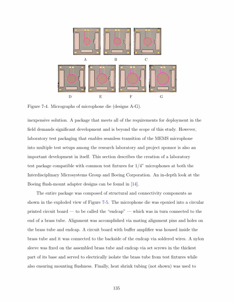
A B C
D E F G
Figure 7-4. Micrographs of microphone die (designs A-G).
inexpensive solution. A package that meets all of the requirements for deployment in the
field demands significant development and is beyond the scope of this study. However,
laboratory test packaging that enables seamless transition of the MEMS microphone
into multiple test setups among the research laboratory and project sponsor is also an
important development in itself. This section describes the creation of a laboratory
test package compatible with common test fixtures for 1/4” microphones at both the
Interdisciplinary Microsystems Group and Boeing Corporation. An in-depth look at the
Boeing flush-mount adapter designs can be found in [14].
The entire package was composed of structural and connectivity components as
shown in the exploded view of Figure 7-5. The microphone die was epoxied into a circular
printed circuit board — to be called the “endcap” — which was in turn connected to the
end of a brass tube. Alignment was accomplished via mating alignment pins and holes on
the brass tube and endcap. A circuit board with buffer amplifier was housed inside the
brass tube and it was connected to the backside of the endcap via soldered wires. A nylon
sleeve was fixed on the assembled brass tube and endcap via set screws in the thickest
part of its base and served to electrically isolate the brass tube from test fixtures while
also ensuring mounting flushness. Finally, heat shrink tubing (not shown) was used to
135

stress-relieve the wires protruding from the brass tube. Brass tubes and nylon sleeves were
provided by Boeing Corporation.
+
Nylon sleeve
)Brass tube
Circuit board
BBBBM
Endcap
6
Mic die
:Wires
Figure 7-5. Exploded view of the laboratory test package.
A closeup rendering of the microphone die in the endcap is shown in Figure 7-6A.
The 0.3485” diameter endcap, a two-layer printed-circuit board laid out in National
Instruments’ Ultiboard software and fabricated at Sierra Protoexpress (Sunnyvale, Ca),
was 0.093” thick to accommodate post-milling of a 500µm deep microphone die recess.
The die recess, epoxy wells, pin holes, and board cut-out were all milled as post-processing
steps at University of Florida using a Sherline Model 2000 CNC mill. Vias on the frontside
were connected to solder pads on the backside for hookup to interface electronics. An
additional via in one epoxy well provided substrate grounding as a precaution against
hard-to-diagnose issues associated with a floating substrate potential. The frontside of the
endcap was plated with soft bondable gold for ease of wire bonding. Figure 7-6B shows
the printed circuit board layout.
The microphone die was epoxied into the endcap in a two stage process using an
EFD Ultimus 2400 Precision Epoxy Dispenser. First, Ablebond 84-1LMI [159] (electrically
conductive silver epoxy) was dispensed in the epoxy well that contained the via and then
the die was placed in the recess. The epoxy was cured in a temperature controlled oven at
150 C for 1 h. Next, Cyberbond DualBond 707 [160] was dispensed in both epoxy wells
136

and cured under a UV lamp for 24 h. During cure, the DualBond 707 became sufficiently
fluid to seep underneath the microphone die and effectively seal the microphone back
cavity. Wire bonds were made with a Kulicke & Soffa 4124 Series Manual Ball Bonding
System and encapsulated with Dow Corning 3145 RTV MIL-A-46146 [161]. Important
settings for epoxy dispensation and wire bonding are found in Table 7-5 and Table 7-6,
respectively. A completed microphone in the endcap package is shown in Figure 7-7.
@@@R
Via for substrateground
Epoxy wells
QQk
@@@I
Vias
>
Mic die
A B
Figure 7-6. Microphone endcap. A) Drawing showing die in place. B) Circuit board layout[162].
Table 7-5. Epoxy dispenser settings.
Ablebond 84-1LMI [159] Dualbond 707 [160] RTV [161]
Pressure [psi] 50 19 60
Back Pressure [mmHg] 16.4 0 7.4
Dispensing Time [s] 1 0.3 Variable
Tip [gauge] 25 25 20
Cure 150 C for 1 h 24 h under UV lamp Room temp. for 2 d
Table 7-6. Wire bond settings.
Ball Bond Wedge Bond
Force 7 7Time 5 5Power 3 4
The circuitry associated with the microphone package — a buffer amplifier with
power supply filter capacitors (0.1µF ceramic and 10µF tantalum) — is shown schematically
137

XXXXXXXXXXXz
Mic Die
HHHHHHHHHj
Endcap
-Wire bondsto Vias
Figure 7-7. Closeup photograph of a packaged MEMS piezoelectric microphone.
in Figure 7-8. The amplifier used was the Linear Technologies LTC6240CS8, which was
chosen for a variety of positive characteristics including low operating current and voltage,
low noise (voltage noise <10 nV/√
Hz), and high input resistance (1 TΩ) [44]. In order to
reduce parasitic capacitance and the associated detrimental effects on device sensitivity
(refer to Section 5.3.1), the amplifier was situated as physically close to the microphone
die as possible. Figure 7-9 shows the circuit board layout. The boards were milled
in-house on thin 0.028” FR4 and components were hand-soldered. Wiring terminated in
banana connectors for v+, v−, and ground, in addition to a BNC connector for the output
signal. The BNC ground was tied to the power supply ground on the board.
One device, 116-1-J7-A, was packaged for different measurements with both a voltage
and charge amplifier. The circuit diagram for the charge amplifier is found in Figure 7-10.
The selected operational amplifier was a Texas Instruments OPA129. The feedback loop
was composed of a 1 GΩ feedback resistor and two 4 pF feedback capacitors in parallel for
a total capacitance of Cfb = 8 pF. These values were chosen to yield close to unity gain
and to maintain a low cut-on frequency. The board layout is not shown but was similar
to that for the voltage amplifier, except with additional length for the inclusion of the
feedback resistor and capacitors.
138

−
+vi
0.1µF
10µFv+
v−
0.1µF
10µF
voLTC6240
Figure 7-8. Voltage amplifier circuitry included in the microphone package.
1.06in.
0.28in. 0.16in.
0.40in.
OutputPads
6Tantalum
CapacitorsJ
JJ]
ElectrolyticCapacitors
@@ILTC6240
6
InputPads
Figure 7-9. Voltage amplifier circuit board layout [162].
Electromagnetic interference (EMI) is a major problem for high-impedance devices
[46] such as the piezoelectric microphone, and steps were taken to mitigate its impact.
The brass tubing was connected to ground to provide a shield for the amplifier circuitry
[46]. In addition, the amplifier board featured a guard ring to help limit leakage
currents into the positive amplifier terminal [44]. Shielded coaxial cable was used for
the microphone output signal.
The completed piezoelectric microphone laboratory test package is shown in
Figure 7-11. The package fits a 3/8” hole with 1/2” depth. Flushness was not characterized
but was estimated to be less than 500µm.
139

−
+
4 pF1GΩ 4pF
vi
0.1µF
10µFv+
v−
0.1µF
10µF
voOPA129
Figure 7-10. Charge amplifier circuit diagram.
Figure 7-11. Complete packaged MEMS piezoelectric microphone.
7.4 Summary
This chapter discussed microphone realization and packaging. The laboratory test
packaged was developed to enable device characterization in measurement setups at both
the Interdisciplinary Microsystems Group and Boeing Corporation. The subject of the
next chapter is experimental characterization of the packaged microphones.
140

CHAPTER 8EXPERIMENTAL CHARACTERIZATION
This chapter describes the thorough experimental characterization of several MEMS
piezoelectric microphones. First, experimental methods are introduced, starting with
die selection and diaphragm topography measurements, then proceeding to acoustic
and electrical characterization. A novel set of parameter extraction experiments are
also described. Experimental setups and data processing techniques are covered. The
experimental results presented thereafter quantify microphone performance in terms
of common metrics, then give way to the results of parameter extraction experiments.
Comparisons to the lumped element model presented in Chapter 5 are also made.
8.1 Experimental Setup
This section provides an overview of the experimental setups used in microphone
selection, characterization, and parameter extraction. The microphone characterization is
divided into acoustic characterization (direct measurements of the microphone response
in a pressure field) and electrical characterization (determination of microphone electrical
traits).
8.1.1 Die Selection Setup
Avago Technologies supplied eight 6” wafers with thousands of die per wafer.
The dicing process discussed in Section 7.2 was carried out on small portions of two
wafers, with a yield of 439 unbroken microphone die. With this many die available for
characterization, an efficient die selection method was needed prior to investing significant
time in the packaging of individual die (as described in Section 7.3).
Electrical measurements are a desirable means of die interrogation because they
can often be done easily at the die level via probing. Electrical impedance is an
obvious quantity to use for discriminating between die. However, the expectation of
mechanical property variations (i.e. stress) being the primary factor separating good
die from bad suggested the need for a more mechanical-oriented selection method.
141

For example, it is shown in Chapter 5 that high values of the effective piezoelectric
coefficient da are associated with both high sensitivity and low noise. By the piezoelectric
constitutive relations (Equation 5–2), da is equivalent to volume displacement per volt
(∀/V ), calculable from an optical scan of the microphone diaphragm under electrical
excitation. Unfortunately, optical scanning of the diaphragm is a time-consuming and
equipment-intensive procedure that is not suited to be performed on a large number of
die. However, da = ∀/V may be rewritten as da = Aeffw/V , where w is the displacement
at an arbitrary diaphragm location and Aeff is an effective area. This suggested that a
quick single point interrogation could still provide useful comparative information.
Another useful metric easily obtainable via optical interrogation of the diaphragm
under electrical excitation is the open-circuit resonant frequency, fr. Tracking shifts
in resonant frequency before and after the packaging process can provide information
about changes in diaphragm stiffness due to unintended packaging stress. In addition,
resonant frequency provides a second comparative measure, and is particularly useful
when selection of like devices is necessary.
The experimental setup is pictured in Figure 8-1. A gridded gel pack with microphone
die in situ was placed directly on the microscope stage of the Polytec scanning laser
vibrometer (LV) system. Each die was interrogated only at a single point, chosen as the
center of the diaphragm for measurement repeatability and to maximize the LV signal.
Probes delivered a periodic chirp signal from the LV function generator (50 Ω output
impedance) to the individual die over a wide frequency range, and the resonant frequency
was selected from the displacement per voltage frequency response function, Hvw (f).
Next, a single tone excitation at 1 kHz was used to find the approximate flat band value of
Hvw, denoted Sa,0. At each stage, the signal power was fine-tuned to obtain greater than
0.98 coherence between excitation signal and LV output. The important measurement
settings are found in Table 8-1.
142

Fiber
Interferometer
Microscope
Stage
Gel pack
w/ mic die To probe
Laser spot
Individual
mic die
Probes
Microscope
Vibrometer
Controller
Scanner
Controller
Sig RefTrig
Sync Velo
Velocity
Laser Vibrometer System
Figure 8-1. Experimental setup for die selection.
Table 8-1. Die selection laser vibrometer settings.
Settings
Parameter Measurement of fr Measurement of Sa,0
Bandwidth 0 kHz to 200 kHz 0 kHz to 20 kHzFFT lines 6400 6400Frequency Resolution 31.25 Hz 3.125 HzAverages 100 (Complex)Excitation Periodic Chirp 1 kHz SineWindow Rectangular
Early in the process, measurements were repeated for several die that were removed
from the gel pack and placed directly on the microscope stage in order to characterize
the impact of the soft acoustic boundary condition presented by the gel. No difference
between measurements was observed, and data in Section 8.2.1 are only given for
microphones tested directly on gel packs.
Outlier rejection was employed before determining the means and standard deviations
associated with Sa,0 and fr for each microphone design. With values of both fr and
143

Sa,0 known for each die, the data were bivariate [163]. As a result, straightforward
univariate outlier detection, such as the Modified Thompson-Tau Technique [164], was not
appropriate. Instead, multivariate outlier detection, which presumes multivariate outliers
are univariate outliers in a particular 1-D projection, was needed [165]. The adjusted
outlyingness (AO) algorithm [166], part of the LIBRA MATLAB toolbox [167, 168]
developed by the Robust Statistics Research Group at the Katholieke Universiteit
Leuven, was used. In the algorithm, a test statistic known as the AO is generated for
each observation over many random 1-D projections, with the maximum AO estimate for
each observation retained. An adjusted boxplot [169] is generated for the AO estimates
and observations whose AO estimates exceed the boxplot upper whisker are regarded as
outliers. The primary assumption of the AO algorithm is unimodality of the data [165].
Griffin et al. provide an accessible introduction to the AO algorithm [165].
After die selection, the same LV measurements used for die selection were repeated
for the endcap-packaged microphone die (recall Section 7.3). For this measurement, the
endcap was simply placed on the microscope stage and probed in a similar manner to the
individual die. The same measurement was also performed prior to packaging of devices
for parameter extraction (details in Section 8.1.5).
8.1.2 Diaphragm Topography Measurement Setup
Microphone die were packaged in multiple rounds, with the first round subjected to
both pre- and post-packaging topographical measurements. The level of static deflection
of the microphone diaphragm, a by-product of film stress, is informative of the diaphragm
stress state. A ZYGO NewView 7200 scanning white light interferometer (SWLI) was used
to perform the measurements. A SWLI works by illuminating a sample with white light,
which reflects off the surface of the sample and recombines with a reference beam, creating
interference fringes . A charge-coupled device (CCD) camera captures the fringes as the
SWLI objective is scanned vertically; the surface topography is deduced from the captured
images via a software algorithm [170]. The NewView 7200 featured a vertical resolution <
144

0.1 nm. Measurements were made with a 5X Michelson objective and 1X field zoom lens,
yielding a measurement area of 1.41 mm×1.05 mm. The standard 640 px × 480 px high
speed camera provided a lateral resolution of approximately 2.2µm. Three averages were
used in all measurements, which were referenced to the surrounding wafer surface. Other
notable software settings are found in Table 8-2.
Table 8-2. Scanning white light interferometer software settings.
Control Parameter Setting
Measurement FDA Res HighACG OnPhase Res Super
Surface Map Remove PlaneRemove Spikes OffDatafill OffFilter OffTrim 0
8.1.3 Acoustic Characterization Setup
Acoustic characterization refers to experimental quantification of the microphone
response to acoustic pressure excitation. The goal of the acoustic characterization was
to quantify the piezoelectric microphone performance in terms of frequency response
(sensitivity, bandwidth) and linearity.
8.1.3.1 Frequency response measurement setup
The frequency response of the piezoelectric microphones, Hm (f) [V/Pa], was
determined over the audio range via a secondary calibration, and the procedures used
hailed from the family of comparison methods [171]. Specifically, the performance of the
DUT was determined via comparison with a measurement-grade reference microphone.
The acoustic characterization was performed in an approximately 1 m-long,
2.2 cm-thick, aluminum plane wave tube (PWT) with a 1 in × 1 in duct. A PWT is a
rigid waveguide designed such that only planar waves propagate below a certain frequency,
called the cut-off frequency of the tube, f c. Below this frequency, higher-order acoustic
145

modes introduced to the PWT are evanescent, meaning they decay exponentially along
its length. Two microphones mounted at the same lengthwise location are therefore
simultaneously exposed to the same pressure for drive frequencies less than f c. For a
square waveguide with cross-sectional dimension a, the cut-off frequency is [28]
f c =c02a
. (8–1)
Equation 8–1 reveals the cut-off frequency may be tuned by the PWT cross-sectional
dimension a or choice of gas. For the purposes of determining the frequency response of
an audio microphone, f c ≥20 kHz is desirable but f c in air for a = 1 in is approximately
6.7 kHz. Helium’s faster isentropic speed of sound makes it possible to increase f c to
approximately 19.8 kHz, allowing for a more comprehensive view of the audio band
response of a microphone.
As a result, complementary frequency response measurements were performed using
both air and helium in the PWT. The measurement in air was intended to yield accurate
sensitivity information under normal operating conditions. The expanded frequency range
of the helium measurement enabled assessment of the flatness of the frequency response
over nearly the full audio range. The use of helium instead of air has a slight effect on the
performances of both the DUT and reference microphones; for example, a helium-filled
cavity is less compliant than an air-filled one, since Cac ∝ 1/ρ0c20 and the ρ0c
20 product
is higher in helium. Lumped element model predictions for the microphone frequency
response in air and in helium are shown in Figure 8-2 for design D. Depending on the
microphone design, the reduction in sensitivity in helium compared to air was predicted to
be 0.04 dB to 0.4 dB.
The experimental setup for the frequency response measurement is shown in
Figure 8-3, with both the reference microphone and DUT mounted at the end of the
PWT. The reference microphone used was a Bruel and Kjær 4138 1/8” pressure field
microphone [50] mounted on a Bruel and Kjær UA0160 adapter and connected to a
146
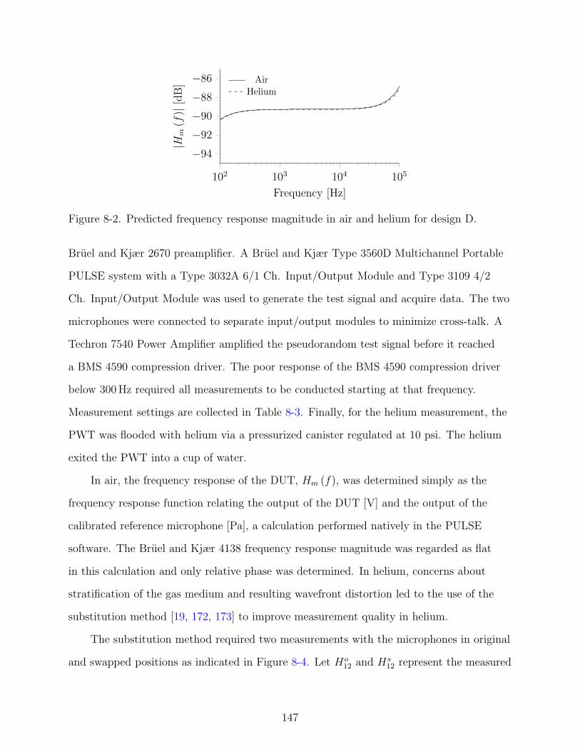
102 103 104 105
−94
−92
−90
−88
−86
Frequency [Hz]
|Hm
(f)|
[dB
] Air
Helium
Figure 8-2. Predicted frequency response magnitude in air and helium for design D.
Bruel and Kjær 2670 preamplifier. A Bruel and Kjær Type 3560D Multichannel Portable
PULSE system with a Type 3032A 6/1 Ch. Input/Output Module and Type 3109 4/2
Ch. Input/Output Module was used to generate the test signal and acquire data. The two
microphones were connected to separate input/output modules to minimize cross-talk. A
Techron 7540 Power Amplifier amplified the pseudorandom test signal before it reached
a BMS 4590 compression driver. The poor response of the BMS 4590 compression driver
below 300 Hz required all measurements to be conducted starting at that frequency.
Measurement settings are collected in Table 8-3. Finally, for the helium measurement, the
PWT was flooded with helium via a pressurized canister regulated at 10 psi. The helium
exited the PWT into a cup of water.
In air, the frequency response of the DUT, Hm (f), was determined simply as the
frequency response function relating the output of the DUT [V] and the output of the
calibrated reference microphone [Pa], a calculation performed natively in the PULSE
software. The Bruel and Kjær 4138 frequency response magnitude was regarded as flat
in this calculation and only relative phase was determined. In helium, concerns about
stratification of the gas medium and resulting wavefront distortion led to the use of the
substitution method [19, 172, 173] to improve measurement quality in helium.
The substitution method required two measurements with the microphones in original
and swapped positions as indicated in Figure 8-4. Let Ho12 and Hs
12 represent the measured
147

Acoustic driver
Plane wave tube
Reference mic
PULSEAmplifier
DUT
He line
He tank
He out
into water
Figure 8-3. Plane wave tube setup for acoustic characterization.
Table 8-3. Settings for microphone frequency response measurements in PULSE.
Grouping Parameter Setting in Air Setting in Helium
Acquisition FFT Type Zoom BasebandCenter Frequency [kHz] 3.5 N/ABandwidth [kHz] 6.4 25.6Frequency Range 300 Hz–6.7 kHz 0 Hz–25.6 kHz# of FFT Lines 6400Frequency Resolution [Hz] 1 4Window RectangularOverlap 0 %# of Averages 100
Generator Signal Pseudo random noiseFrequency Range 300 Hz–6.7 kHz 300 Hz–25.9 kHzSpectral Lines 6400
frequency response functions in the original and swapped positions, respectively, relating
the output of microphone 2 (the DUT) to that of microphone 1 (the reference) in units of
V/V. Also let the frequency response functions of the two microphones be denoted H1 and
H2 [V/Pa]. In the original and swapped positions depicted in Figure 8-4,
148

a
b
Mic 1
Mic 2
A
Mic 1
Mic 2a
b
B
Figure 8-4. Microphone switching procedure. A) Original positions. B) Swapped positions.
Ho12 =
Go12
Go11
= Hab
(
H∗1H2
H∗1H1
)
(8–2)
and
Hs12 =
Gs12
Gs11
= Hba
(
H∗1H2
H∗1H1
)
, (8–3)
where ∗ denotes complex conjugate, G12 cross-spectral density, G11 is autospectral density,
and Hab and Hba [Pa/Pa] are frequency response functions relating the actual pressures at
the two measurement locations. A key assumption of Equations 8–2 and 8–3 is that there
is no change in the pressure field between measurements, i.e. the pressures at location
a and location b remain unchanged. To help adhere to this assumption, no alterations
to the state of the measurement setup, particularly the acoustic source, were made
between measurements save for swapping of the microphones, which was accomplished via
removing and rotating the PWT endplate. Multiplying Equations 8–2 and 8–3 together,
noting that HabHba = 1, taking the square root, and rearranging,
H2 = H1
√
Ho12H
s12. (8–4)
Therefore, with the frequency response function of the reference microphone, H1,
well-known, the frequency response function of the DUT, Hm (f) = H2 (f), can be
149

deduced from the geometric mean of measurements for Ho12 and Hs
12 even when the
two microphones are not exposed to precisely the same pressure. Over the range of
measurement frequencies, it is sufficient to regard H1 as having constant magnitude [50]
and non-constant phase. The phase roll-off is approximately 7.5 by 20 kHz [174].
Due to the low-frequency limitations of the BMS 4590 compression driver used in
the PWT setup, additional measurements to characterize the low-frequency roll-off of
the piezoelectric microphone were performed at Boeing Corporation. Two piezoelectric
microphones, 138-1-I2-D and 138-1-J3-F, were transferred to Boeing for this measurement
and others. The measurement setup is pictured in Figure 8-5 and consisted of the DUT
and Bruel and Kjær 4136 reference microphone mounted in a small acoustic cavity
(though Figure 8-5B shows 2 Bruel and Kjær 4136 microphones mounted there) that was
driven by a speaker and terminated into an “infinite” (100 ft) copper tube. The infinite
tube termination was actually designed to suppress the formation of standing waves and
enable high frequency measurements, but this existing setup was still attractive for the
low frequency measurement.
An HP 35670 spectrum analyzer provided a broadband white noise signal and
acquired the DUT and reference microphone signals. Measurement settings are found
in Table 8-4. Using the spectrum analyzer, the frequency response function relating the
DUT output to the calibrated reference microphone output [V/Pa] was calculated. The
frequency response function was then post-processed to correct for the low-frequency
roll-off in the reference microphone. The low-frequency calibration of the reference
microphone was obtained at 1/3 octave bands down to 10 Hz using a Bruel and Kjær
UA0033 electrostatic actuator with a G.R.A.S. actuator supply Type 14AA. The typical
−3 dB lower limiting frequency for a Bruel and Kjær 4136 is 0.3 Hz to 3 Hz.
8.1.3.2 Linearity measurement setup
Characterization of microphone linearity refers to the quantification of how the
voltage output of the DUT changes with sound pressure level. Measurements were
150
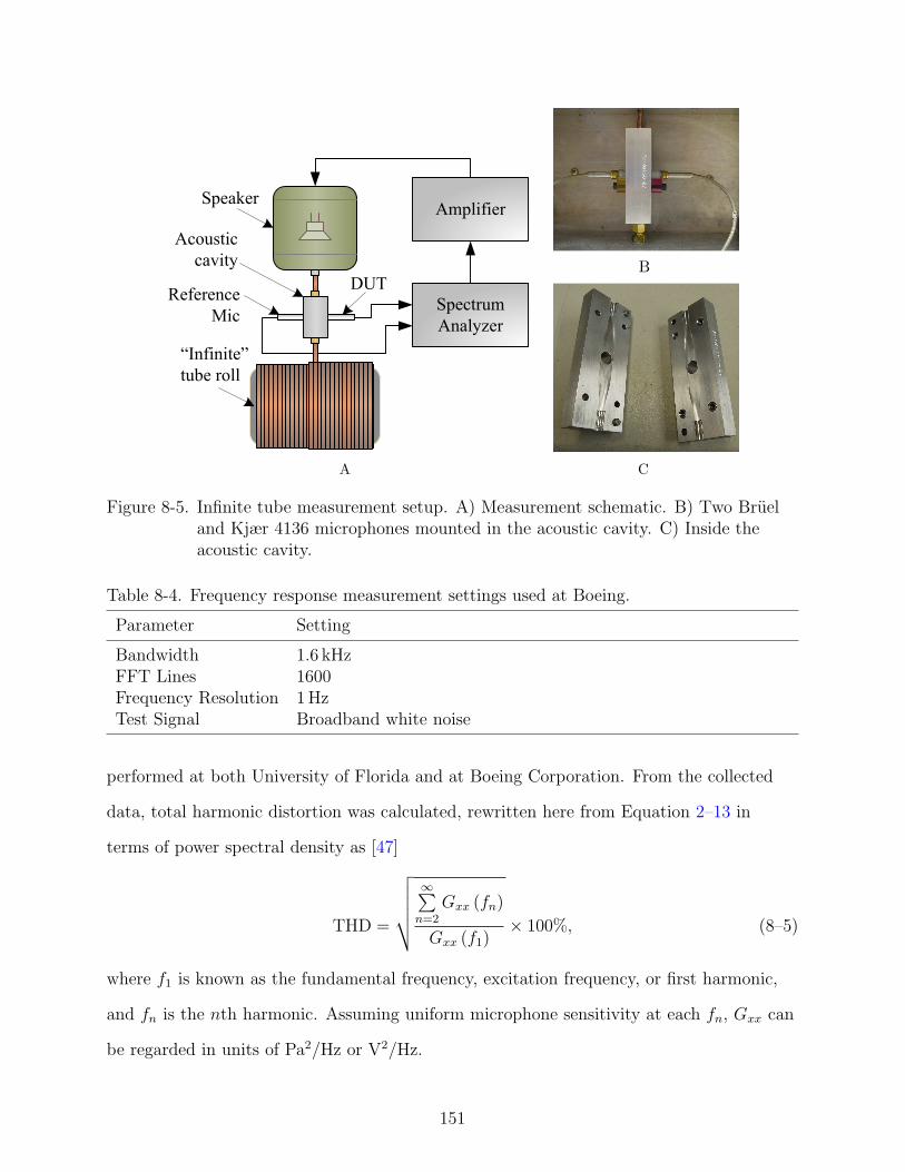
Amplifier
Spectrum
Analyzer
Speaker
“Infinite”
tube roll
DUTReference
Mic
Acoustic
cavity
A
B
C
Figure 8-5. Infinite tube measurement setup. A) Measurement schematic. B) Two Brueland Kjær 4136 microphones mounted in the acoustic cavity. C) Inside theacoustic cavity.
Table 8-4. Frequency response measurement settings used at Boeing.
Parameter Setting
Bandwidth 1.6 kHzFFT Lines 1600Frequency Resolution 1 HzTest Signal Broadband white noise
performed at both University of Florida and at Boeing Corporation. From the collected
data, total harmonic distortion was calculated, rewritten here from Equation 2–13 in
terms of power spectral density as [47]
THD =
√
√
√
√
√
∞∑
n=2
Gxx (fn)
Gxx (f1)× 100%, (8–5)
where f1 is known as the fundamental frequency, excitation frequency, or first harmonic,
and fn is the nth harmonic. Assuming uniform microphone sensitivity at each fn, Gxx can
be regarded in units of Pa2/Hz or V2/Hz.
151

At University of Florida, the same setup used to find the frequency response (in
air), pictured in Figure 8-3, was used to obtain data for the total harmonic distortion
calculation. A single tone signal at 1 kHz drove the BMS 4590 compression driver, which
could reach a SPL of approximately 160 dB without exceeding its power rating. A PCB
Piezotronics Model 377A51 precision condenser microphone, with a maximum SPL of
192 dB (3 % distortion), was connected to a Bruel and Kjær 2670 preamplifier and served
as the reference. The DUT and reference microphone output signals were collected using
the same settings found in Table 8-3 at multiple pressure levels. Starting from the lowest
SPL with a detectable 2nd harmonic, the SPL was increased in steps of 3–4 dB SPL up
to 160 dB. The 6.4 kHz bandwidth enabled the first six harmonics to be captured. An
important consideration in getting a reliable pressure reference using the PWT for this
measurement was that harmonics higher than the 6th propagate as higher-order modes
and thus do not contribute equally to the response of the DUT and reference microphone.
Therefore, power distributed to frequencies fn for n > 6 must be negligible in order for the
calculation to be valid.
Experimental results to be discussed in Section 8.2.3.2 show that the setup of
Figure 8-3, apart from the microphones, suffers from significant harmonic contamination.
Speaker distortion is one contributor, together with harmonic generation during nonlinear
acoustic propagation at high sound pressure levels [28]; the latter source of distortion
worsens with propagation distance.
A measurement setup at Boeing Corporation was designed specifically to minimize
harmonic contamination at high sound pressure levels. Photographs of the setup are
found in Figure 8-6. The measurement apparatus, an acoustical coupler [35], was better
known as “the wedge,” inside of which was a low-volume cavity driven by four manifolded
speakers. A reference microphone (in this case the Bruel and Kjær 4938 1/4” pressure
field microphone with Bruel and Kjær 2670-W-001 preamplifier) and the DUT were
mounted facing each other, as shown in Figure 8-6B, at close proximity (0.231”). A single
152

PPPPqWedge
DUT
>
Speakers
A
@@@R
Reference mic
DUT
*
Wedge
B
Figure 8-6. Linearity measurement setup at Boeing Corporation. A) View of the entirewedge fixture, with speakers. B) Reference microphone and DUT mounted inthe wedge. Photographs courtesy of Boeing Corporation.
tone signal at 2.5 kHz was chosen based on the speaker’s frequency response characteristics
to provide the highest sound pressure levels. The maximum SPL achievable in the wedge
was approximately 172 dB and was limited by the speakers’ power rating. Measurement
settings for an HP35670A spectrum analyzer, used to collect the data and perform the
THD calculation with ten harmonics included, are found in Table 8-5.
Table 8-5. Total harmonic distortion measurement settings used at Boeing.
Parameter Setting
Bandwidth 25.6 kHzFFT Lines 400Frequency Resolution 64 HzWindow FlattopFundamental Frequency 2.5 kHz# of Harmonics 10
8.1.4 Electrical Characterization Setup
There were two major goals in the electrical characterization of the piezoelectric
microphones. First, the microphone’s noise floor was measured to enable calculation of
the important minimum detectable pressure metric. In addition, electrical elements found
in the lumped element model of Chapter 5, including Ceb (or Cef ), Ceo, Rep, and Res,
153

were extracted from impedance measurements. Finally, the total parasitic capacitances
that served to attenuate the microphone sensitivities from open circuit values, Cep + Cea,
were estimated for a single device via data from a combination of electrical and acoustic
measurements.
8.1.4.1 Noise floor measurement setup
This section details the measurement strategy for the microphone’s intrinsic noise
floor. Section 2.3.2 addressed the presence of both intrinsic and extrinsic noise in sensors.
The intrinsic noise floor is of primary importance because it indicates the best-achievable
noise characteristics of the MEMS microphones when effectively shielded from extrinsic
noise sources. Referring the intrinsic electrical output noise to the microphone input yields
the minimum detectable pressure of the microphone.
The measurement setup [38] is pictured in Figure 8-7. The DUT is placed inside
a triple Faraday cage, which serves to attenuate electromagnetic interference from the
lab environment. Two sets of AA batteries powered the DUT buffer amplifier at ±3 V.
The DUT output signal was fed through the innermost Faraday cage to the middle
Faraday cage, where it was connected to a Stanford Research Systems (SRS) Model SR560
Low-Noise Preamplifier (itself battery-powered) and amplified by a factor of 1000. The
amplifier output was then fed through the outer two Faraday cages to a SRS Model SR785
2 Channel Dynamic Signal Analyzer. A custom-programmed Labview VI performed the
data collection via computer control of the SR785 and saved the measured output power
spectral density [V2/Hz].
Measurement settings are found in Table 8-6. The noise power spectral density of
the DUT was collected over a total bandwidth from 0 Hz to the maximum frequency of
102.4 kHz using multiple separate measurements, each with the instrument maximum
800 FFT lines. Employing multiple frequency spans enabled measurements with better
frequency resolution at low frequencies and more blocks at high frequencies, where
measurement time was dramatically reduced. The start and end frequencies, frequency
154
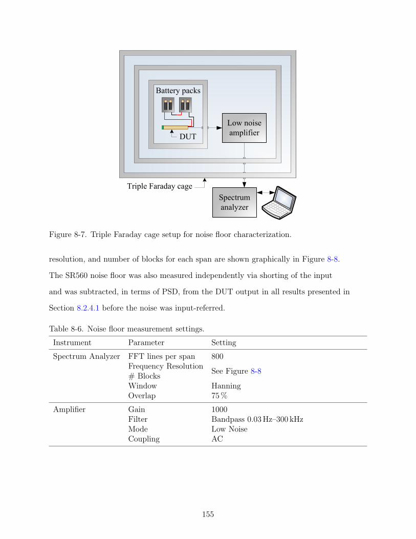
Low noise
amplifierDUT
Battery packs
Triple Faraday cage
Spectrum
analyzer
Figure 8-7. Triple Faraday cage setup for noise floor characterization.
resolution, and number of blocks for each span are shown graphically in Figure 8-8.
The SR560 noise floor was also measured independently via shorting of the input
and was subtracted, in terms of PSD, from the DUT output in all results presented in
Section 8.2.4.1 before the noise was input-referred.
Table 8-6. Noise floor measurement settings.
Instrument Parameter Setting
Spectrum Analyzer FFT lines per span 800Frequency Resolution
See Figure 8-8# BlocksWindow HanningOverlap 75 %
Amplifier Gain 1000Filter Bandpass 0.03 Hz–300 kHzMode Low NoiseCoupling AC
155

0 6.4 12.8 25.6 38.4 51.2 76.8 102.4
8 8 16 16 16 32 32
1k 1k 5k 5k 10k 10k 10k
∆f [Hz]
f [kHz]
# Blocks
Figure 8-8. Noise floor measurements spans, frequency resolution, and averages.
8.1.4.2 Impedance measurement setup
The goal of the electrical impedance measurement was to obtain impedance data from
which electrical parameters could be extracted. In Section 5.2.4, an expression was derived
for the electrical impedance of a piezoelectric microphone,
Zeq = Res +Rep
1 + jωRep (Cef + Ceo), (8–6)
Using this equation, the elements Res, Rep, and Cef + Ceo were extracted from impedance
measurements performed on 2 of each design from wafer 116 section 3 (14 measured die in
total). An HP 4294A impedance analyzer [175] together with a Cascade Microtech M150
probe station were used to perform the measurement. The HP 4294A utilizes the accurate
low-frequency auto-balancing-bridge method [176, 177] and a four terminal configuration
that reduces the effects of lead impedances on the measurement [176]. The measurement
setup is shown in Figure 8-9. The two terminals of each pair (Lc/Lp and Hc/Hp) come
together at the very tip of the probe needle and all four terminal grounds were connected
at the probe input. Calibration was performed using a GGB Industries CS-8 impedance
standard substrate of the ground-short (GS) configuration. A custom-written program in
HP Instrument BASIC collected and stored 31 complete impedance measurement sweeps
for each device (no on-board averaging), enabling post-processing to establish confidence
bounds. Measurement settings are found in Table 8-7.
For a capacitance-dominated device approximately in the range of 1–10 pF,
the maximum bias error was not guaranteed in the operation manual [175] to be
below 10% until the measurement frequency exceeded between 0.4 and 4 kHz. The
provided bias error prediction equations were in fact invalid for impedances exceeding
156

Lc Lp Hp Hc
Impedance Analyzer
DUTProbe Station
Probe
Figure 8-9. Impedance measurement setup using a probe station.
Table 8-7. Impedance measurement settings.
Parameter Setting
Sweep Type LogarithmicSweep Range 1 kHz to 200 kHzNumber of Points 801Point Delay Time 0 sSweep Delay Time 0 sOscillator Level 500 mVDC Bias OffBandwidth 3Sweep Averaging OffPoint Averaging Off
approximately 100 MΩ, where maximum bias error predictions easily surpassed 100%
[178]. As a result, the measurement was conducted starting from 1 kHz, at which a 4 pF
capacitance measurement was guaranteed to have < 10 % bias error (or < 3 % for a 16 pF
measurement). The instrument-minimum frequency was 40 Hz.
Although impedance was the measurand, admittance is often a more convenient
representation for piezoelectrics. Impedance data post-processed into admittance form
(Yeq = 1/Zeq) was used for the model fit,
Yeq =jωRep (Cef + Ceo) + 1
(jωRep (Cef + Ceo) + 1)Res + Rep
, (8–7)
The benefit of the admittance form is that when Res is small, the admittance reduces to
the very simple expression Yeq ≈ 1/Rp + jω (Cef + Ceo). The fit to Equation 8–7 was
performed using the MATLAB function invfreqs, which like most curve-fitting tools
157

attempts to minimize the weighted sum of the squared residuals between the data and
fit at each measurement point. The particular benefit of invfreqs is that it is specifically
formulated to fit transfer functions to complex frequency response data. The form of
Equation 8–7 that MATLAB uses for fitting is
Yeq =B1s + B2
A1s + A2
, (8–8)
where A1 = 1 always by convention. Comparing to Equation 8–7, the electrical parameters
were extracted as
Cef + Ceo =B1
A2 −B2/B1
, (8–9)
Rep =A2
B2
− 1
B1
, (8–10)
and
Res =1
B1
. (8–11)
A statistical distribution for these parameters was obtained via repeated fitting to
perturbed mean measurements in Monte Carlo simulations. From these distributions, the
mean and 95% confidence interval were calculated. Further details on the Monte Carlo
simulations and accompanying uncertainty analysis are found in Section C.4.
8.1.4.3 Parasitic capacitance extraction setup
The expressions for the frequency response of a microphone packaged with a charge
or voltage amplifier were developed in Section 5.2.3, including approximate expressions for
flatband sensitivity. From those expressions, it is possible to estimate parasitic capacitance
and open-circuit sensitivity with appropriate measurements. Equations 5–47 and 5–53
predict the flatband sensitivity for a microphone packaged with a voltage amplifier and
charge amplifier, respectively. Equating the open circuit sensitivity, Soc, that appears in
Equations 5–47 and 5–53 and rearranging yields an estimate for parasitic capacitance,
Cep + Cea =Sca
Sva
Cfb − (Cef + Ceo) . (8–12)
158

To make use of this expression, frequency response measurements replace the single-valued
sensitivities in Equation 8–12 to yield
Cep + Cea =Hm,ca (f)
Hm,va (f)Cfb − (Cef + Ceo) , (8–13)
where Hm,ca and Hm,va represent the frequency response functions [V/Pa] associated
with a single microphone packaged consecutively with a charge and voltage amplifier.
Microphone 116-1-J7-A was packaged solely for this purpose. Packaged with the voltage
amplifier architecture, microphone 116-1-J7-A shared common electronics architecture,
including consistent trace lengths, amplifier, etc. with the other piezoelectric microphones;
this suggested consistent parasitic capacitance could be expected. With the parasitic
capacitance known for 116-1-J7-A and assuming that it remained essentially unchanged
from device-to-device, the open circuit sensitivity of all microphones was estimated from
the rearranged Equation 5–47,
Soc = SvaCef + Ceo + Cep + Cea
Cef + Ceo
. (8–14)
Estimating the open-circuit sensitivities of the microphones in this way also enabled
avoidance of the substantial risk of damage associated with packaging and re-packaging all
of the microphones with both voltage and charge amplifier architectures.
Measurements of Hm,ca and Hm,va for microphone 116-1-J7-A were performed in air
using the same PWT setup described in Section 8.1.3.1. Values for Cef + Ceo values were
obtained from impedance measurements presented in Section 8.2.4.2 under the assumption
that electrical properties were consistent device-to-device.
8.1.5 Electroacoustic Parameter Extraction
Extraction of electroacoustic parameters enables validation of individual lumped
element predictions. Relatively simple elements representing, for example, the acoustic
back cavity are well-known [28]. However, elements whose values are predicted from the
diaphragm model, including the diaphragm compliance Cad and mass Mad, in addition to
159

the effective piezoelectric coefficient da, require validation. In this section, experiments
for their extraction are described, with the approach driven by the more demanding
needs for extraction of compliance and mass. A measurement procedure for microphone
sensitivity compatible with the requirements of the parameter extraction experiment is
also addressed.
8.1.5.1 Compliance and mass measurement setup
The diaphragm compliance and mass, as defined in Section 5.2.1.2, are calculated
from the diaphragm displacement due to pressure loading. In nomenclature appropriate
for the measurement setting, they may be redefined as
Cad =
∫ 2π
0
∫ a2
0
Hpw|V=0 (r, θ)rdrdθ (8–15)
and
Mad =
∫ 2π
0
∫ a20
ρa Hpw|2V=0 (r, θ)rdrdθ[
∫ 2π
0
∫ a20
Hpw|V=0 (r, θ)rdrdθ]2 , (8–16)
where Hpw|V=0 [m/Pa] is the frequency response function obtained under short-circuit
conditions relating the location-dependent displacement w (r, θ) to pressure acting on the
diaphragm, a2 is the outer diaphragm diameter, and ρa is the aerial density, defined in
Equation 5–13. Note that because ρa changes abruptly at r = a1, the integral over r in the
numerator of Equation 8–16 must be evaluated piece-wise.
From Equations 8–18 to 8–16, extraction of Cad and Mad requires the ability to apply
a known pressure to the diaphragm while optically scanning its displacement. Although
a measurement setup could be devised that would allow simultaneous excitation and
optical measurement of the packaged microphones, the design of measurement fixtures
providing optical access for a laser vibrometer system within its depth-of-field would be
a significant challenge and expense. Instead, a simpler measurement setup was used in
which specially-packaged microphones were excited with a known pressure via their back
cavities and the accompanying diaphragm displacement was measured from the front side.
160

The packaging requirements for this measurement were dictated largely by the desire
to use an existing pressure coupler [149]. Together with the need for compatibility with
the pressure coupler, the need to enable measurements of microphone frequency response
functions via inclusion of integrated interface electronics led to the choice of a circuit
board to house the microphone die. A 0.059 in thick board milled in-house from FR-4,
with the microphone die epoxied into a recess at one end, was used. An exploded view
of the pressure coupler assembly and packaging solution are shown in Figure 8-10. The
circuit board was clamped into position over the open topside of the pressure coupler’s
acoustic cavity with a Lucite end plate. A 0.03 in (762µm) diameter hole centered within
the die recess in the circuit board coupled the microphone back cavity with the pressure
coupler cavity, while an optical window on the front side enabled laser access to the
diaphragm, as shown in Figure 8-11.
The pressure coupler provided two access points for acoustic pressure measurements
within the cavity. A reference microphone was mounted at normal incidence in a plug that
inserted into the end of the cavity, as labeled in Figure 8-10. Meanwhile, the DUT was
mounted at grazing incidence approximately 9 mm up the cavity. For low frequency sound
with wavelength much greater than this dimension, the pressures were approximately
equal. The pressures at the reference microphone and DUT locations were 90 out of
phase at quarter wavelength separation (9.5 kHz driving frequency in air).
In Chapter 5, Cad and Mad were extracted from the theoretical prediction of static
diaphragm deflection. They are equivalently calculable from dynamic measurements at
sufficiently low frequencies (i.e. frequencies much lower than the resonant frequency of
the diaphragm). With resonant frequencies upwards of 100 kHz for all devices measured,
excitation at 1 kHz was sufficiently low to be considered quasi-static. The wavelength at
1 kHz (34 cm) was also 38 times the test and reference microphone separation and thus
more than sufficient to regard the pressures at the two locations as nearly equal. This was
confirmed experimentally.
161

@@
@@@@
@@@R
Opticalwindow
*
Referencemic port
HHHHHHj
Mic die
JJ
JJ]
Circuit board
ZZ
ZZZZ~
Acousticcavity
1Pressurecoupler
End plate
9
Interfaceelectronics
Speakerconnection
Figure 8-10. Pressure coupler assembly (fasteners not shown).
The measurement setup for extraction of acoustic mass and compliance is shown in
Figure 8-12. A 1 kHz sinusoid generated by an Agilent 33120A function generator1 and
1 Although the laser vibrometer system possesses its own function generator as part of the scannercontroller, intermittent problems with prolonged usage of sinusoids led to the use of the external functiongenerator.
162

AAAK
BacksidePressure
Excitation
Scanning Laser
Figure 8-11. Closeup depiction of a microphone die in the pressure coupler setup.
amplified via a Stewart Electronics PA-1008 200 Watt Power Amplifier drove the BMS
4590P compression driver. The reference microphone was amplified using a SRS Model
SR560 Low-Noise Preamplifier and the amplified signal served as the reference in the laser
vibrometer system’s native data acquisition system. The reference microphone calibration
was entered directly into the laser vibrometer software to avoid the need to adjust data in
a post-processing step. The velocity signal from the laser vibrometer itself was the other
input for the two-channel system. Specific measurement settings are collected in Table 8-8.
Table 8-8. Pressure coupler measurement settings.
Parameter Setting
Span 5 kHzFFT Lines 400Resolution 12.5 Hz# of averages 100 (Complex)Window RectangularSignal 1 kHz SineLV sensitivity DC 1 mm/s/VTypical pressure level 95 dB to 105 dBSR560 gain 100
Diaphragm scans were taken over polar grids of 20 azimuthal points and 13-15
radial points, depending on diaphragm size; Figure 8-13 shows one such grid. Prior to
integration, the actual measured data — which was returned from the laser vibrometer
system as a scattered dataset — was interpolated to form a surface via MATLAB’s
163

DUT epoxied in
circuit board
Pressure Coupler
Acoustic Driver
Reference
Mic Amplifier
Fiber
Interferometer
Vibrometer
Controller
Scanner
Controller
RefTrig
Velo
Velocity
Amplifier
Function
GeneratorOut
Sync
Laser Vibrometer System
Microscope
Figure 8-12. Experimental setup for extraction of acoustic mass and compliance.
TriScatteredInterp [138]. Independent surfaces were created for the real and imaginary
part of the frequency response function and then recombined for integration in MATLAB’s
numerical routine dblquad [138], which employs Gauss quadrature over a rectangular
domain in two dimensions. The integration was performed in r-θ space using surfaces
originally interpolated in Cartesian space.
500µm
Figure 8-13. Laser vibrometer scan grid overlayed on design E micrograph (diaphragmouter diameter of 756µm).
164

In order to predict the quality of the interpolation and integration routine apriori,
a test numerical integration was performed using an analytical expression for the typical
static deflection shape of a clamped plate subjected to a uniform pressure load [121],
w (r) = w0
[
1 −(r
a
)2]2
, (8–17)
interpolated at the actual measurement scan points. Error was found to be approximately
1 % relative to the associated analytical volume displacement, ∆∀ = w0a2π/3. The
integration procedure was also compared to trapezoidal integration of the same test
problem and it was confirmed that the Gauss quadrature routine was more accurate by
several tenths of a percent.
8.1.5.2 Frequency response measurement setup
The requirement of short circuit conditions, in addition to input channel limitations
of the laser vibrometer system, did not enable simultaneous acquisition of microphone
electrical output during the actual parameter extraction experiment. Instead, the
electrical acquisition was done in a separate measurement, also in the pressure coupler, to
determine the microphone sensitivities.
Pressure Coupler
Acoustic Driver PULSE
AmplifierReference
Mics
Figure 8-14. Experimental setup for pressure coupler calibration.
First, the relationship between the pressures at the two measurement locations was
confirmed via the experimental setup pictured in Figure 8-14, in which two Bruel and
Kjær 4138 microphones were mounted at the reference and DUT positions. The frequency
165
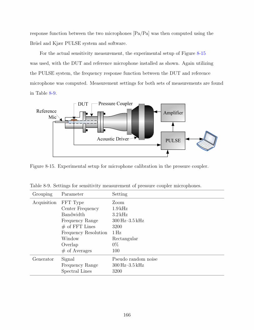
response function between the two microphones [Pa/Pa] was then computed using the
Bruel and Kjær PULSE system and software.
For the actual sensitivity measurement, the experimental setup of Figure 8-15
was used, with the DUT and reference microphone installed as shown. Again utilizing
the PULSE system, the frequency response function between the DUT and reference
microphone was computed. Measurement settings for both sets of measurements are found
in Table 8-9.
DUT Pressure Coupler
Acoustic Driver PULSE
AmplifierReference
Mic
Figure 8-15. Experimental setup for microphone calibration in the pressure coupler.
Table 8-9. Settings for sensitivity measurement of pressure coupler microphones.
Grouping Parameter Setting
Acquisition FFT Type ZoomCenter Frequency 1.9 kHzBandwidth 3.2 kHzFrequency Range 300 Hz–3.5 kHz# of FFT Lines 3200Frequency Resolution 1 HzWindow RectangularOverlap 0%# of Averages 100
Generator Signal Pseudo random noiseFrequency Range 300 Hz–3.5 kHzSpectral Lines 3200
166

8.1.5.3 Effective piezoelectric coefficient measurement setup
The expression for the effective piezoelectric coefficient, Equation 5–8, may be written
for the measurement setting as
da =
∫ 2π
0
∫ a2
0
Hvw|p=0 (r, θ)rdrdθ, (8–18)
where Hvw is the frequency response function relating the displacement w (r, θ) to an
excitation voltage. The subscript p=0 follows from the theoretical definition of da and
denotes an acoustic short circuit condition. Such a condition is only achievable for
excitation well below the vent/cavity break frequency, which based on other sensitivity
measurements must be in the vicinity of 50 Hz. Because the measurand of the laser
vibrometer, velocity, is ∝ f for a harmonic input [34], the signal-to-noise ratio of the
measurement degrades considerably at low frequencies. Instead, Hvw|p=0 was obtained
via excitation at 1 kHz. The diaphragm displacement due to voltage excitation for the
Fiber
Interferometer
Packaged
device To probe
Microscope
Vibrometer
Controller
Scanner
Controller
Ref Trig
Velo
Velocity
Scanning
laser
Function
GeneratorOut
Sync
Probe
Microscope
stage
Laser Vibrometer System
Figure 8-16. Experimental setup for extraction of effective piezoelectric coefficient.
167
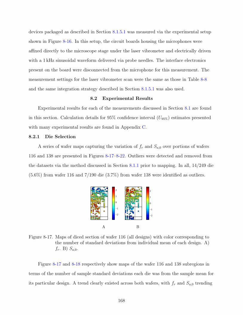
devices packaged as described in Section 8.1.5.1 was measured via the experimental setup
shown in Figure 8-16. In this setup, the circuit boards housing the microphones were
affixed directly to the microscope stage under the laser vibrometer and electrically driven
with a 1 kHz sinusoidal waveform delivered via probe needles. The interface electronics
present on the board were disconnected from the microphone for this measurement. The
measurement settings for the laser vibrometer scan were the same as those in Table 8-8
and the same integration strategy described in Section 8.1.5.1 was also used.
8.2 Experimental Results
Experimental results for each of the measurements discussed in Section 8.1 are found
in this section. Calculation details for 95% confidence interval (U95%) estimates presented
with many experimental results are found in Appendix C.
8.2.1 Die Selection
A series of wafer maps capturing the variation of fr and Sa,0 over portions of wafers
116 and 138 are presented in Figures 8-17–8-22. Outliers were detected and removed from
the datasets via the method discussed in Section 8.1.1 prior to mapping. In all, 14/249 die
(5.6%) from wafer 116 and 7/190 die (3.7%) from wafer 138 were identified as outliers.
−2
−1
0
1
2
A
−2
−1
0
1
2
B
Figure 8-17. Maps of diced section of wafer 116 (all designs) with color corresponding tothe number of standard deviations from individual mean of each design. A)fr. B) Sa,0.
Figure 8-17 and 8-18 respectively show maps of the wafer 116 and 138 subregions in
terms of the number of sample standard deviations each die was from the sample mean for
its particular design. A trend clearly existed across both wafers, with fr and Sa,0 trending
168

−2
0
2
A
−2−101
B
Figure 8-18. Maps of diced section of wafer 138 (all designs) with color corresponding tothe number of standard deviations from individual mean of each design. A)fr. B) Sa,0.
oppositely with respect to each other across wafer 116 but largely the same way with
respect to each other across wafer 138.
140
145
150
155
A
135
140
145
B
120
125
130
135
C
110
112
114
116
118
120
122
D
95
100
105
110
115
E
94
96
98
100
102
F
90
95
100
G
Figure 8-19. Resonant frequency maps for wafer 116 [kHz]. A) Design A. B) Design B. C)Design C. D) Design D. E) Design E. F) Design F. G) Design G.
Figure 8-19 and Figure 8-20 show fr and Sa,0, respectively, for wafer 116 in individual
maps for each design. Trends are clear for designs A–D, with resonant frequency
increasing away from the wafer center and displacement sensitivity decreasing. In
Figure 8-19(E–G), the lack of a corresponding cross-wafer trend in fr for designs E–G,
with larger diaphragms that are more susceptible to buckling, may indicate the diaphragm
response to stress is not stable die-to-die for these designs.
169

2
2.2
2.4
2.6
2.8
3
3.2
A
1.8
2
2.2
2.4
2.6
2.8
B
1.4
1.6
1.8
2
2.2
C
1.2
1.3
1.4
1.5
1.6
1.7
1.8
D
0.8
1
1.2
1.4
1.6
1.8
E
0.6
0.8
1
1.2
F
0.5
1
1.5
G
Figure 8-20. Center displacement sensitivity maps for wafer 116 [nm/V]. A) Design A. B)Design B. C) Design C. D) Design D. E) Design E. F) Design F. G) DesignG.
Maps for fr and Sa,0 on wafer 138, Figure 8-21 and 8-22, respectively, show an
entirely different trend than wafer 116. On wafer 138, the resonant frequency and
sensitivity both decrease together toward the outside of the wafer and the trend is
consistent for all designs.
Table 8-10 collects the sample means (denoted with overbars) and sample standard
deviations (s) of fr and Sa,0 for each design. As expected, the resonant frequency
decreases with design letter, reflecting the expected increase in compliance with diaphragm
size. Perhaps unexpectedly, Sa,0 actually decreases with diaphragm size for wafer 116, but
again the buckled nature of those diaphragms makes drawing conclusions difficult. For
wafer 138, Sa,0 remains essentially constant for all designs, which is also unexpected. It is
shown in Section 8.2.5 that the nearly constant Sa,0 across all designs is only indicative of
a consistent center deflection and that contrary to expectations, the piezoelectric coupling
coefficient does not necessarily trend strongly with center deflection.
170

180
200
A
160
170
180
B
130
140
150
C
110
120
130
D
100105110115
E
859095100
F
80
90
G
Figure 8-21. Resonant frequency maps for wafer 138 [kHz]. A) Design A. B) Design B. C)Design C. D) Design D. E) Design E. F) Design F. G) Design G.
1.21.41.61.8
A
11.21.41.61.8
B
1.21.41.61.8
C
0.811.21.41.61.8
D
0.811.21.41.61.8
E
1
1.5
F
1
1.5
G
Figure 8-22. Center displacement sensitivity maps for wafer 138 [nm/V]. A) Design A. B)Design B. C) Design C. D) Design D. E) Design E. F) Design F. G) DesignG.
One or more microphones of several designs were selected to be packaged for rigorous
characterization and parameter extraction. For each design, the die with the highest
values of Sa,0 were generally selected for packaging as microphones with the expectation
that the piezoelectric coupling coefficient da, and thus sensitivity, would trend similarly.
Section 8.2.5 addresses the validity of this assumption. As the only other comparative
measure available, fr was used as a second metric for choosing like microphones of the
171

Table 8-10. Wafer statistics.
Wafer 116 Wafer 138
fr [kHz] Sa,0 [nm/V] fr [kHz] Sa,0 [nm/V]
Design fr sfr Sa,0 sSa,0 fr sfr Sa,0 sSa,0
A 149.4 7.2 2.7 0.3 195.0 10.0 1.6 0.3B 138.5 5.7 2.2 0.2 166.0 8.8 1.6 0.4C 129.3 4.4 1.8 0.3 142.9 8.9 1.6 0.3D 118.1 4.4 1.5 0.2 122.4 7.9 1.5 0.4E 109.0 5.3 1.3 0.3 107.5 5.8 1.5 0.4F 100.1 3.4 1.1 0.2 95.8 6.1 1.5 0.3G 92.6 3.9 0.9 0.3 83.6 6.6 1.5 0.3
Table 8-11. Pre- and post-packaging LV measurements.
Pre-Packaging Post-Packaging
DUT fr [kHz] Sa,0 [nm/V] fr [kHz] Sa,0 [nm/V]
116-1-I6-A 147.3 3.18 127.0 3.79116-1-C4-B 133.0 2.51 127.5 2.17116-3-F7-B 144.0 2.08 160.3 1.88116-1-E2-C 124.9 2.11 123.5 2.10138-1-E4-D 132.6 1.80 126.9 1.89138-1-I2-D 133.5 1.91 116.5 1.68138-1-I8-E 114.4 1.85 106.4 1.63138-1-H3-F 103.9 1.82 99.9 1.45138-1-J3-F 103.9 1.87 129.5 1.46
same design. In all, 10 die were successfully shepherded through the packaging process
described in Section 7.3, with one used exclusively for the parasitic capacitance extraction.
Pre- and post-packaging laser vibrometer measurements of the nine packaged
microphones are collected in Table 8-11 . Changes in resonant frequency were likely due
to inadvertent introduction of packaging stress to the microphone diaphragm during the
die epoxy step, which modifies the effective compliance of the diaphragm. A corresponding
change in Sa,0 due to packaging stress was also observed. Figure 8-23 shows that the shifts
in fr and Sa,0 following the packaging process were not at all consistent, particularly the
direction of the shifts. This suggests the epoxy is not entirely consistent; some notable
172

I6-A
C4-B
F7-B
E2-C
E4-D
I2-D
I8-E
H3-
FJ3
-F
−20
−10
0
10
20
DUT
%C
han
ge
frS
Figure 8-23. Changes in resonant frequency and displacement sensitivity due to packaging.
possibilities that were not investigated further are uneven sealing of the microphone die to
the board or epoxy penetrating slightly into the back cavity.
8.2.2 Diaphragm Topography
The diaphragm static deflection profiles for pre- and post-packaged microphones
are shown in Figures 8-24A–8-24B, respectively. Six devices representing one batch of
packaged sensors are included, and just the inner regions of the diaphragms are shown for
clarity. Displacements are referenced to the surrounding substrates and were taken along a
line bisecting the diaphragm through the vent hole.
Microphone C4-B, the only device included in Figure 8-24 that hailed from wafer
116, is shown to be significantly buckled. This was expected given the visible buckling
of all devices on wafer 116. The total deflection over the inner portion of the diaphragm
before packaging was approximately 2.7µm compared to a total thickness in that region of
2.14µm. The static deflection profiles of the unpackaged microphones hailing from wafer
138 were consistent and much lower than microphone C4-B, typically about 300 nm from
edge to center.
After packaging, the buckled amplitude of C4-B was reduced to approximately
2.3µm and the static deflection profiles of the wafer 138 devices were no longer as tightly
grouped. Figure 8-25 shows the differences in static deflection after the packaging process,
173

−400 −200 0 200 400
−1
0
1
2
Substrate
Radius [µm]
Sta
tic
Defl
ecti
on[µ
m]
116-1-C4-B
138-1-E4-D
138-1-I2-D
138-1-I8-E
138-1-H3-F
138-1-J3-F
A
−400 −200 0 200 400
−1
0
1
2
Substrate
Radius [µm]
Sta
tic
Defl
ecti
on[µ
m]
116-1-C4-B
138-1-E4-D
138-1-I2-D
138-1-I8-E
138-1-H3-F
138-1-J3-F
B
Figure 8-24. Static deflection profiles of several microphone diaphragms (inner portions).A) Before packaging. B) After packaging.
−400 −200 0 200 400−0.6
−0.4
−0.2
0
0.2
Radius [µm]Sta
tic
Defl
ecti
onD
iff.
[µm
]
116-1-C4-B
138-1-E4-D
138-1-I2-D
138-1-I8-E
138-1-H3-F
138-1-J3-F
Figure 8-25. Static deflection differences for pre- and post-packaged microphones.
which were typically around 10 nm in total for wafer 138 microphones and clearly not of
an axially symmetric nature.
174

8.2.3 Acoustic Characterization
8.2.3.1 Frequency response
The frequency response function measurements made in helium are collected in
Figure 8-26, shown in terms of magnitude and relative phase to the reference microphone.
The frequency response magnitude is flat to well within the stated goal of ±2 dB over
the portion of the audio band measured (300 Hz–20 kHz). Deviations in the magnitude
and phase close to 20 kHz are the result of higher-order acoustic modes beginning to
propagate. Note that the phase is relative to the Bruel and Kjær 4138. The microphones
were phase-matched to <2 out to 15 kHz.
0 5 10 15 20−100
−95
−90
−85
−80
Mag
nit
ud
e[d
Bre
1V/P
a]
116-1-I6-A
116-1-C4-B
116-3-F7-B
116-1-E2-C
138-1-E4-D
138-1-I2-D
138-1-I8-E
138-1-H3-F
138-1-J3-F
0 5 10 15 200
45
90
135
180
Frequency [kHz]
Rel
ativ
eP
has
e[
] 116-1-I6-A
116-1-C4-B
116-3-F7-B
116-1-E2-C
138-1-E4-D
138-1-I2-D
138-1-I8-E
138-1-H3-F
138-1-J3-F
Figure 8-26. Microphone frequency responses in helium.
The sensitivities of the MEMS microphones are collected in Table 8-12 in both dB
and µV/Pa for measurements performed in air. The sensitivities in helium were all lower
than in air as expected, by up to 0.2 dB (2.3 %). The phase roll-off in helium was less than
in air by approximately 5 at 6 kHz.
175

Table 8-12. Microphone frequency response characteristics† at 1 kHz in air.
Magnitude
DUT dB re 1 V/Pa µV/Pa Relative Phase []
116-1-I6-A −90.68 ± 0.06 29.2 ± 0.2 176.8 ± 0.1116-1-C4-B −89.24 ± 0.06 34.5 ± 0.2 177.6 ± 0.1116-3-F7-B −90.87 ± 0.06 28.6 ± 0.2 177.0 ± 0.1116-1-E2-C −88.52 ± 0.06 37.5 ± 0.2 177.6 ± 0.1138-1-E4-D −89.86 ± 0.06 32.1 ± 0.2 177.3 ± 0.1138-1-I2-D −89.77 ± 0.06 32.5 ± 0.2 177.9 ± 0.1138-1-I8-E −88.71 ± 0.06 36.7 ± 0.2 178.1 ± 0.1138-1-H3-F −87.19 ± 0.06 43.7 ± 0.3 178.3 ± 0.2138-1-J3-F −88.25 ± 0.06 38.7 ± 0.3 178.0 ± 0.2
† Uncertainties are for 95% confidence interval (see Section C.2).
The normalized frequency response measurements for microphones 138-1-I2-D and
138-1-J3-F obtained at low frequencies in Boeing Corporation’s “infinite” tube setup are
captured in Figure 8-27. The −2 dB frequencies for 138-1-I2-D and 138-1-J3-F were 85 Hz
and 69 Hz, respectively, which compared well with theoretical predictions of 70 Hz and
75 Hz.
8.2.3.2 Linearity
Figure 8-28 shows plots of DUT voltage versus the reference microphone pressure
level (both taken at the fundamental frequency of 1 kHz) in both linear units and decibels
for 7 of the 9 microphones. Some variation from linearity can be detected for several
devices in Figure 8-28A, most notably 116-1-I6-A and 116-1-C4-B. The response of the
remaining two devices, 116-3-F7-B and 116-1-E2-C, are shown in Figure 8-29, with abrupt
deviations from linearity happening near 1000 Pa and 1500 Pa, respectively. This behavior
can likely be attributed to sudden snap-through of the buckled diaphragms, a nonlinear
dynamic event. Further investigation of this unwanted phenomenon is beyond the scope of
this study, but the interested reader is referred to various texts on nonlinear dynamics of
structures [179, 180].
176

101 102 103
−4
−2
0
Nor
m.
Mag
nit
ud
e[d
B]
138-1-I2-D
138-1-J3-F
101 102 103
−5
0
5
Frequency [Hz]
Nor
m.
Ph
ase
[]
138-1-I2-D
138-1-J3-F
Figure 8-27. Piezoelectric microphone frequency response functions at low frequenciesnormalized to values at 1 kHz
The THD calculations for all 9 microphones are shown in Figure 8-30. The large
levels of distortion (30–40%) for the reference microphone, which by specification should
not exceed 3% until 190 dB, indicate the measurement environment is harmonic-rich.
Nonlinearities in the amplifier, speaker, and acoustic propagation path are all possible
contributors. As a result, the calculated THD of Figure 8-30 are not valid in an
absolute sense, though comparison to the reference microphone “THD” provides valuable
qualitative information. For DUT THD that aligns closely enough to that of the reference
(as is the case with all wafer 138 microphones), one can be reasonably confident that the
distortion limit is well above 160 dB. The same cannot be said definitively for the wafer
116 microphones, which exhibit varying levels of deviation from the reference microphone
“THD.”
The results of the Boeing linearity measurements are collected in Table 8-13. The
calculated total harmonic distortion in both the DUT and reference microphone are given
for each test, and SPLs are reported as the pressure measured at 2.5 kHz (the fundamental
177

0 500 1,000 1,500 2,0000
25
50
75
Pressure [Pa]V
olta
ge[m
V] 116-1-I6-A
116-1-C4-B138-1-E4-D138-1-I2-D138-1-I8-E138-1-H3-F138-1-J3-F
A
60 80 100 120 140 160−120−100−80−60−40−20
SPL [dB re 20 µPa]
Vol
tage
[dB
re1
V]
116-1-I6-A116-1-C4-B138-1-E4-D138-1-I2-D138-1-I8-E138-1-H3-F138-1-J3-F
B
Figure 8-28. Linearity measurements. A) Linear scale. B) In dB.
0 500 1,000 1,500 2,0000
255075
100125
Pressure [Pa]
Vol
tage
[mV
] 116-3-F7-B116-1-E2-C
Figure 8-29. Linearity measurements showing unusual nonlinear behavior.
frequency) using each microphone. Because both the Bruel and Kjær 4938 and DUT
distort while also serving as sources of the SPL measurement, the reported SPLs must be
regarded as lower bounds on the distortion limits. That is, reported distortion occurs at a
SPL greater than that given here. Therefore, the device 138-1-J3-F almost certainly meets
the 172 dB specification for PMAX given in Section 1.2.
178

100 120 140 160
0
10
20
30
SPL [dB]
TH
D[%
] 116-1-I6-APCB 377A51
A
100 120 140 160
0
10
20
SPL [dB]
TH
D[%
] 116-1-C4-BPCB 377A51
B
100 120 140 160
0
20
40
SPL [dB]
TH
D[%
] 116-3-F7-BPCB 377A51
C
100 120 140 160
0
20
40
SPL [dB]
TH
D[%
] 116-1-E2-CPCB 377A51
D
100 120 140 160
0
10
20
30
SPL [dB]
TH
D[%
] 138-1-E4-DPCB 377A51
E
100 120 140 160
0
10
20
30
SPL [dB]
TH
D[%
] 138-1-I2-DPCB 377A51
F
100 120 140 160
0
10
20
30
SPL [dB]
TH
D[%
] 138-1-I8-EPCB 377A51
G
100 120 140 160
0
10
20
30
SPL [dB]
TH
D[%
] 138-1-H3-FPCB 377A51
H
100 120 140 160
0
10
20
30
SPL [dB]
TH
D[%
] 138-1-J3-FPCB 377A51
I
Figure 8-30. THD measurements. A) 116-1-I6-A. B) 116-1-C4-B. C) 116-1-F7-B. D)116-1-E2-C. E) 138-1-E4-D. F) 138-1-I2-D. G) 138-1-I8-E. H) 138-1-H3-F. I)138-1-J3-F.
179
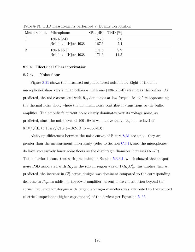
Table 8-13. THD measurements performed at Boeing Corporation.
Measurement Microphone SPL [dB] THD [%]
1 138-1-I2-D 166.0 3.0Bruel and Kjær 4938 167.6 2.4
2 138-1-J3-F 171.6 2.9Bruel and Kjær 4938 171.3 11.5
8.2.4 Electrical Characterization
8.2.4.1 Noise floor
Figure 8-31 shows the measured output-referred noise floor. Eight of the nine
microphones show very similar behavior, with one (138-1-I8-E) serving as the outlier. As
predicted, the noise associated with Rep dominates at low frequencies before approaching
the thermal noise floor, where the dominant noise contributor transitions to the buffer
amplifier. The amplifier’s current noise clearly dominates over its voltage noise, as
predicted, since the noise level at 100 kHz is well above the voltage noise level of
8 nV/√
Hz to 10 nV/√
Hz (−162 dB to −160 dB).
Although differences between the noise curves of Figure 8-31 are small, they are
greater than the measurement uncertainty (refer to Section C.3.1), and the microphones
do have successively lower noise floors as the diaphragm diameter increases (A→F).
This behavior is consistent with predictions in Section 5.3.3.1, which showed that output
noise PSD associated with Rep in the roll-off region was ∝ 1/RepC2et; this implies that as
predicted, the increase in C2et across designs was dominant compared to the corresponding
decrease in Rep. In addition, the lower amplifier current noise contribution beyond the
corner frequency for designs with large diaphragm diameters was attributed to the reduced
electrical impedance (higher capacitance) of the devices per Equation 5–65.
180

101 102 103 104 105
−160
−140
−120
Frequency [Hz]
Noi
seP
SD
[dB
reV
/Hz
1 2]
116-1-I6-A116-1-C4-B116-3-F7-B116-1-E2-C138-1-E4-D138-1-I2-D138-1-I8-E138-1-H3-F138-1-J3-F
Figure 8-31. Output-referred noise floors.
101 102 103 104 105
20
40
60
80
Frequency [Hz]
MD
P[d
Bre
20µ
Pa/
Hz1
/2]
116-1-I6-A116-1-C4-B116-3-F7-B116-1-E2-C138-1-E4-D138-1-I2-D138-1-I8-E138-1-H3-F138-1-J3-F
Figure 8-32. Minimum detectable pressure spectra.
Figure 8-32 shows the minimum detectable pressure spectra of the microphones,
calculated from the measured output noise PSD Svo as
MDP = 20 log10
√
Svo/ |Sva|2
20µPa/Hz1/2
, (8–19)
with |Sva| taken from Table 8-12. Because |Sva| is a flatband sensitivity value, this
calculation is not valid in the vicinity of and beyond f±2 dB.
Due to differences in sensitivity, the minimum detectable pressure curves are less
tightly grouped compared to the output-referred equivalents. Figure 8-32 shows that the
noise floor in the audio band is below 70 dB for all microphones, and below the target
1 kHz narrow bin MDP of 48.5 dB, save for the outlier, 138-1-I8-E. By 20 kHz, minimum
181

detectable pressure levels decline to 25–30 dB SPL. The uncertainties in the MDP spectra
range from ±0.10 dB in the first two frequency spans (< 12.8 kHz) down to ±0.04 dB
above 38.4 kHz; refer to Section C.3.1 for details.
101 102 103 104 105
−160
−140
−120
Frequency [Hz]Noi
seP
SD
[dB
re1
V/H
z1/2]
Voltage AmpCharge Amp
A
101 102 103 104 105
40
60
80
Frequency [Hz]MD
P[d
Bre
20µ
Pa/
Hz1
/2]
Voltage AmpCharge Amp
B
Figure 8-33. Noise floor spectra for 116-1-J7-A with a voltage amp and charge amp. A)Noise PSD. B) MDP.
The noise floor spectra for device 116-1-J7-A packaged with a voltage and charge
amplifier are given in Figure 8-33. Figure 8-33A shows that the noise spectra of the
system is nearly 10 dB higher when the device is packaged with a charge amplifier. For the
charge amplifier case at low frequencies, the equivalent resistor Rep ‖ Refb is a source of
more noise than just Rep in the voltage amplifier case. At higher frequencies, it is likely
that the approximately 2× greater voltage noise of the OPA129 amplifier used in the
charge amplifier circuit compared to the LTC6240 amplifier used in the voltage amplifier
circuit dominates, especially given the extra gain factor for this noise source associated
with the charge amplifier circuitry, (1 + Cet/Cefb)2 (per Equation 5–75). In terms of MDP,
the charge amplifier configuration yields a minimum detectable pressure approximately
6.5 dB greater than that of the voltage amplifier configuration, even despite the higher
sensitivity of the microphone for the former (discussed in Section 8.2.4.3).
From the data presented in Figure 8-32, several variants on minimum detectable
pressure were computed and are presented in Table 8-14 with estimated 95% confidence
182

Table 8-14. Minimum detectable pressure metrics.
DUT dB† dB OASPL‡ dB(A) OASPL§
116-1-J7-A# 54.3 95.1 88.6116-1-J7-A 47.6 88.1 82.0116-1-I6-A 45.7 87.2 80.4116-1-C4-B 43.7 85.6 78.1116-3-F7-B 45.5 87.2 80.4116-1-E2-C 42.8 85.0 77.3138-1-E4-D 43.5 85.3 78.3138-1-I2-D 43.9 85.3 78.2138-1-I8-E 50.6 89.2 86.3138-1-H3-F 40.2 82.7 75.0138-1-J3-F 40.4 83.2 75.4
† Narrow bin (f = 1kHz, ∆f = 1Hz); |U95%| < 0.10 dB ‡ |U95%| < 0.01 dB § |U95%| < 0.007 dB(A)# Packaged with charge amplifier
intervals (refer to Section C.3 for details). First, the already-discussed narrow bin MDP
is given. The second and third columns of Table 8-14 contain integrated measures of
MDP, the overall sound pressure level (OASPL) and A-weighted overall sound pressure
level (AOASPL). In both cases, integration of the noise floor was completed over the
individual 1/3 octave bands from 20 Hz–20 kHz, with A-weighting [33] also employed in
the latter case before final summation. Every microphone had an MDP more than 3 dB
below the specification of 93 dB OASPL except 116-1-J7-A packaged with the charge
amplifier. The A-weighted MDP is lower in all cases because A-weighting de-emphasizes
noise contributions at frequencies below 1 kHz, where the MDP spectrums are the highest.
8.2.4.2 Impedance
A typical impedance measurement, presented in terms of the real and imaginary
components of admittance (conductance, G, and susceptance, B) are found in Figure 8-34.
The standard and overall uncertainties associated with G and B are also included. The
curve fit does an excellent job matching susceptance, which is capacitance-dominated;
typical R-squared values for that fit were unity. The general character of the conductance
is also captured, though clearly there is room for improvement in the model; typical
183

103 104 105
10−8
10−7Conductance,G
[S]
Measured Fit
103 104 105
10−11
10−10
10−9
10−8
Uncertainty
Bounds[S] sG bG U95%
103 104 105
10−7
10−6
10−5
Frequency [Hz]
Susceptance,B
[S]
Measured Fit
103 104 105
10−10
10−8
Frequency [Hz]
Uncertainty
Bounds[S] sB bB U95%
Figure 8-34. Admittance measurements and fits for microphone B5-E.
R-squared values for this fit were 0.84. Note that the resonance at approximately 118 kHz
is not captured due to simplifications made in the equation for electrical impedance
Extracted parameters, together with their 95% confidence bounds, are collected
and compared with the theory in Table 8-15, in which the final letter in the DUT label
continues to stand for the design. Capacitance predictions are within 7 % to 15 % of
extracted values, with the predictions improving with diaphragm size. The difference
between measured and theoretical values is essentially constant at approximately 1 pF
for all designs, suggesting the presence of additional parasitics and/or inherent bias
in the parallel plate capacitance prediction. It is well-known that the parallel-plate
approximation tends to underpredict capacitance, with the underprediction becoming
more severe as lateral dimensions approach the electrode separation distance [181].
8.2.4.3 Parasitic capacitance extraction
Figure 8-35 shows the frequency response functions of microphone 116-1-J7-A
packaged with a voltage and charge amplifier. The microphone’s sensitivity when packaged
184

Table 8-15. Extracted electrical parameters.
Measurement† Theory‡
DUT Cef + Ceo [pF] Rep [MΩ] Res [kΩ] Cef + Ceo [pF] Rep [MΩ]
116-3-B9-A 6.9 ±0.03 % 96 ±4 % 2.6 ±2 % 5.9 401116-3-C5-A 6.9 ±0.03 % 98 ±4 % 2.5 ±2 % 5.9 401116-3-B8-B 7.5 ±0.03 % 131 ±7 % 2.5 ±2 % 6.5 362116-3-C6-B 7.5 ±0.03 % 127 ±7 % 2.4 ±2 % 6.5 362116-3-B7-C 8.2 ±0.03 % 122 ±6 % 2.0 ±2 % 7.2 326116-3-C7-C 8.2 ±0.02 % 120 ±7 % 2.0 ±2 % 7.2 326116-3-C8-D 9.1 ±0.02 % 116 ±6 % 1.6 ±2 % 8.2 286116-3-E9-D 9.2 ±0.02 % 115 ±6 % 1.6 ±2 % 8.2 286116-3-B5-E 10.2 ±0.02 % 116 ±6 % 1.3 ±2 % 9.2 253116-3-C9-E 10.1 ±0.02 % 113 ±6 % 1.3 ±2 % 9.2 253116-3-B4-F 11.3 ±0.02 % 115 ±6 % 1.0 ±2 % 10.4 225116-3-C10-F 11.3 ±0.02 % 116 ±6 % 1.0 ±2 % 10.4 225116-3-B1-G 12.8 ±0.02 % 112 ±6 % 0.9 ±2 % 12.0 195116-3-D5-G 12.8 ±0.02 % 112 ±6 % 0.9 ±2 % 12.0 195
† Uncertainties are 95% confidence intervals in the curve fit ‡ Res = 4.1 kΩ
with the charge amplifier was approximately 3 dB (1.4×) higher, indicating the parasitic
capacitance did indeed play a prominent role in limiting the sensitivity of the device. The
phase component of Figure 8-35 shows the output of the microphone with charge amp was
180 out of phase with the voltage amplifier configuration, as predicted in Equations 5–53
and 5–53.
The extracted parasitic capacitance Cep + Cea is plotted against frequency in
Figure 8-36 together with its 95% confidence interval (see Section C.5). The parasitic
capacitance was relatively constant over the measurement bandwidth, indicating the
character of its impact was captured accurately by the models. Taking the mean of each of
the curves, a single extracted value for Cep is approximately 4 pF ± 1 pF. The uncertainty
analysis, found in Section C.5, suggests that Cfb is a dominant error source. Also note
that the measured capacitance approximating Cef + Ceo were selected from the B9-A and
C5-A die.
185
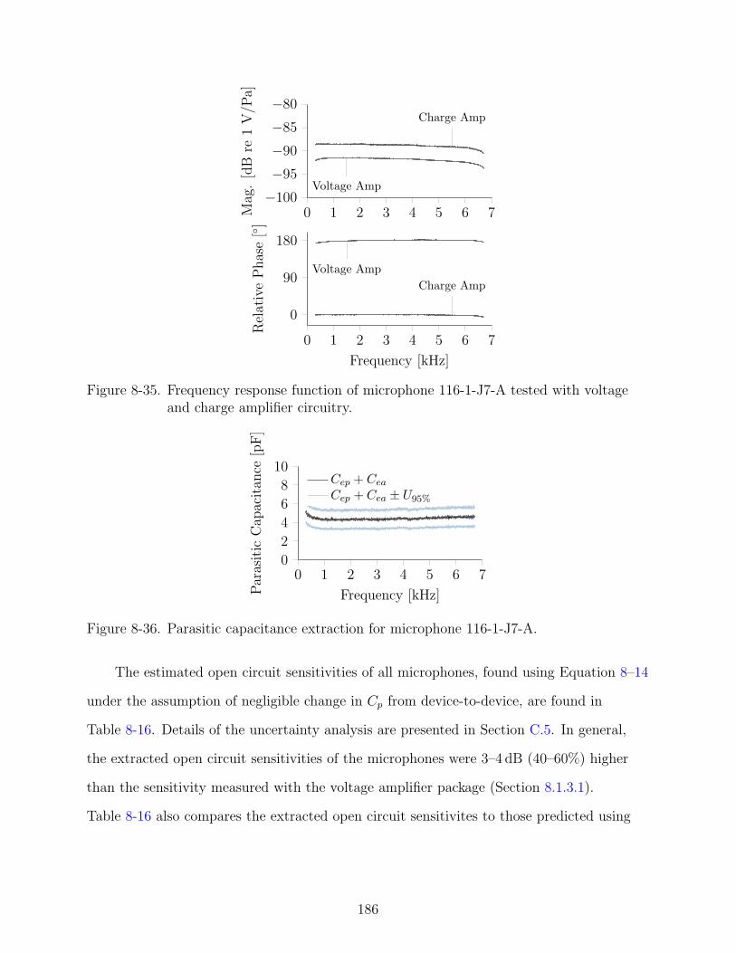
0 1 2 3 4 5 6 7−100
−95
−90
−85
−80Charge Amp
Voltage Amp
Mag
.[d
Bre
1V/P
a]
0 1 2 3 4 5 6 7
0
90
180
Charge Amp
Voltage Amp
Frequency [kHz]
Rel
ativ
eP
has
e[
]
Figure 8-35. Frequency response function of microphone 116-1-J7-A tested with voltageand charge amplifier circuitry.
0 1 2 3 4 5 6 70
2
4
6
8
10
Frequency [kHz]Par
asit
icC
apac
itan
ce[p
F]
Cep + Cea
Cep + Cea ± U95%
Figure 8-36. Parasitic capacitance extraction for microphone 116-1-J7-A.
The estimated open circuit sensitivities of all microphones, found using Equation 8–14
under the assumption of negligible change in Cp from device-to-device, are found in
Table 8-16. Details of the uncertainty analysis are presented in Section C.5. In general,
the extracted open circuit sensitivities of the microphones were 3–4 dB (40–60%) higher
than the sensitivity measured with the voltage amplifier package (Section 8.1.3.1).
Table 8-16 also compares the extracted open circuit sensitivites to those predicted using
186

Table 8-16. Open-circuit sensitivity estimates.
Soc† [dB re 1 V/Pa]
DUT Measured‡ Predicted Soc − Sva‡ [dB re 1 V/Pa]
116-1-J7-A -87.2 ± 0.8 -89.8 4.2 ± 0.8
116-1-I6-A -86.4 ± 0.8 -89.8 4.3 ± 0.8116-1-C4-B -85.2 ± 0.8 -88.7 4.0 ± 0.8116-3-F7-B -86.8 ± 0.8 -88.7 4.0 ± 0.8116-1-E2-C -84.8 ± 0.7 -87.7 3.7 ± 0.7138-1-E4-D -86.4 ± 0.7 -86.6 3.4 ± 0.7138-1-I2-D -86.4 ± 0.7 -86.6 3.4 ± 0.7138-1-I8-E -85.6 ± 0.6 -85.6 3.1 ± 0.6138-1-H3-F -84.3 ± 0.6 -84.6 2.9 ± 0.6138-1-J3-F -85.4 ± 0.6 -84.6 2.9 ± 0.6
† Taken at 1 kHz ‡ With 95% confidence bounds (Section C.5)
the lumped element model. The agreement is excellent for wafer 138, but not so for the
buckled devices of wafer 116.
8.2.5 Electroacoustic Parameter Extraction
Prior to performing measurements directly for electroacoustic parameter extraction,
the pressure coupler assembly was characterized. Figure 8-37 shows the “gain” (really
attenuation) between the DUT position and reference mic position. At 1 kHz the pressure
was shown to be approximately 1.5 % less at the DUT location. Extracted parameters
were therefore corrected for this difference in pressure.
Uncorrected frequency response measurements for each of the specially-packaged
parameter extraction microphones are presented in Figure 8-38. The sensitivities trend
lower than like designs measured in the PWT, suggesting increased parasitic capacitance
was associated with the package for this experiment. This was not unexpected, as the
FR4 boards in which microphones were packaged featured longer trace lengths, different
routing of traces, extra solder connections, etc. Measurement uncertainty (95% confidence)
was <1% and dominated by bias error in the reference microphone calibration (see
Section C.2).
187

0 1 2 30
0.5
1
1.5
Gai
n[P
a/P
a]
0 1 2 3−90
−45
0
45
90
Frequency [kHz]
Ph
ase
[]
Figure 8-37. Comparison of pressure at test and reference locations in pressure coupler.
Mode shapes associated with the diaphragm displacement response under pressure
loading, Hpw, are collected in Figure 8-39. In addition to surface maps, profiles taken
through x = 0 and y = 0 are projected on the plot back planes to enable comparison.
A clear trend of increasing center displacement and volume displacement from design
D to design F is observed, providing an immediate visual indication that the measured
compliance increases with diaphragm size. The corresponding mode shape predictions
(incremental deflection) obtained from the static diaphragm model ranged from
approximately 0.2 nm/Pa to 0.3 nm/Pa, lower than the observed 0.4 nm/Pa to 0.65 nm/Pa
in Figure 8-39.
The acoustic compliance and mass extracted from the mode shapes of Figure 8-39
are presented in Table 8-17, with both compliance and mass trending as the models. The
measured and predicted values of Mad agreed to within 10%, though it is important
to acknowledge that both values shared a common input — the aerial density ρa
associated with the diaphragm materials (Equation 5–13). In general, the resolution
188

0 1 2 3
−94
−92
−90
−88
−86
Sen
siti
vit
y[d
Bre
1V/P
a]
138-1-B6-D
138-1-F5-D
138-1-C9-E
138-1-D9-E
138-1-F7-F
0 1 2 3−90
−45
0
45
90
Frequency [kHz]
Ph
ase
[]
138-1-B6-D
138-1-F5-D
138-1-C9-E
138-1-D9-E
138-1-F7-F
Figure 8-38. Frequency response of piezoelectric microphones in pressure coupler.
of a lumped element model is expected to be on the order of 10%. Measurement of Cad,
which possessed no such shared input, yielded nearly double the predicted value, though
extracted values for like designs were consistent to within <7 %. Measurement uncertainty
estimates were calculated via Monte Carloa simulation as addressed in Section C.6.
The under-prediction of Cad via the diaphragm model could stem from one of several
sources. Finite element analysis validation of an example microphone in Section 5.2.5
was in close agreement with the analytical predictions, but this analysis shared the same
model inputs for residual stresses, material properties, etc. Error in residual stress inputs
could have a significant impact on the model predictions. In addition, the geometry in
both the analytical diaphragm model and finite element model was simplified from the
true geometry, which does not truly possess the sharp step discontinuity at r = a1. A
final possibility is compliance in the boundary conditions of the diaphragm, which would
189

−5000
500
−500
0
5000
0.4
0.8
µmµm
Hpw
[nm/P
a]
A
−5000
500
−500
0
5000
0.4
0.8
µmµm
Hpw
[nm/P
a]
B
−5000
500
−500
0
5000
0.4
0.8
µmµm
Hpw
[nm/P
a]
C
−5000
500
−500
0
5000
0.4
0.8
µmµm
Hpw
[nm/P
a]
D
−5000
500
−500
0
5000
0.4
0.8
µmµm
Hpw
[nm/P
a]
E
−5000
500
−500
0
5000
0.4
0.8
µmµm
Hpw
[nm/P
a]
F
Figure 8-39. Displacement per pressure plots. A) 138-1-B6-D. B) 138-1-F5-D. C)138-1-C9-E. D) 138-1-D9-E. E) 138-1-F7-F. F) 138-1-H7-F.
190
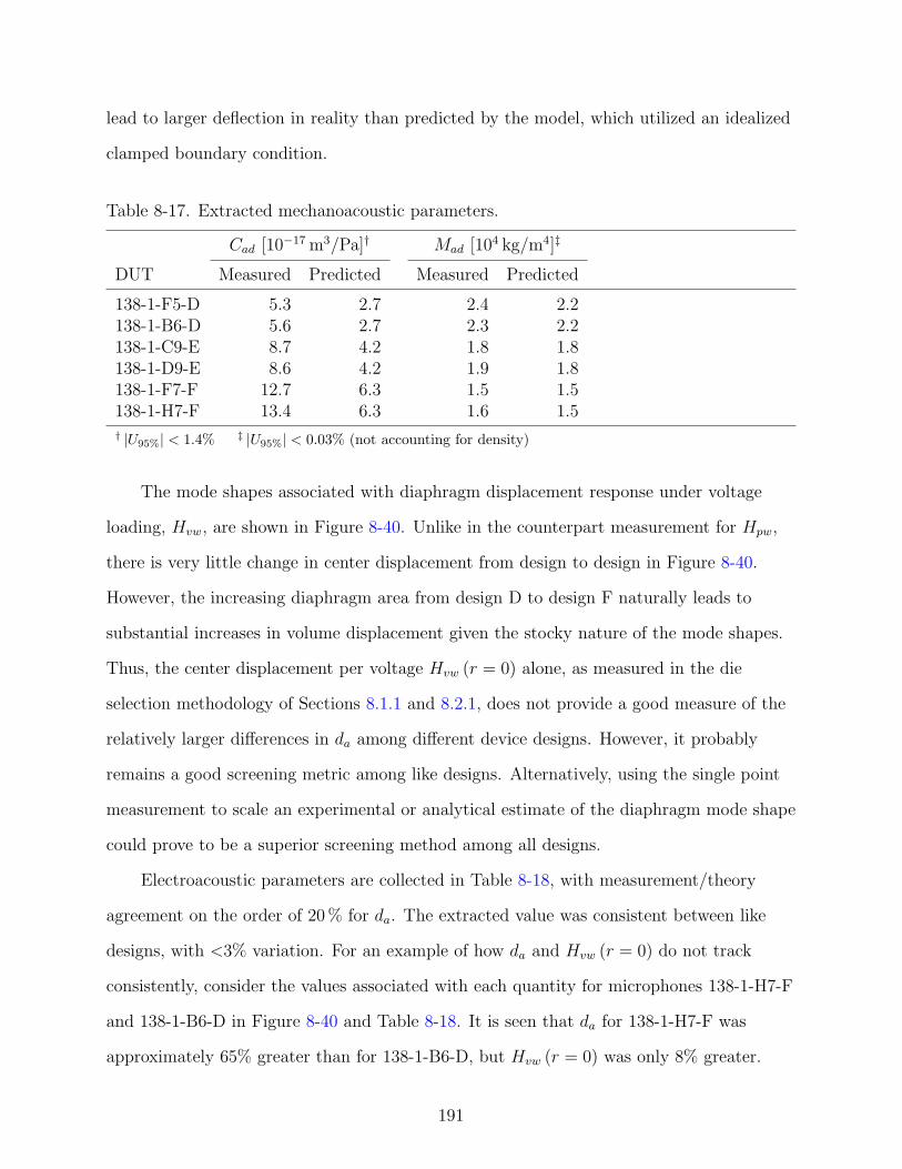
lead to larger deflection in reality than predicted by the model, which utilized an idealized
clamped boundary condition.
Table 8-17. Extracted mechanoacoustic parameters.
Cad [10−17 m3/Pa]† Mad [104 kg/m4]‡
DUT Measured Predicted Measured Predicted
138-1-F5-D 5.3 2.7 2.4 2.2138-1-B6-D 5.6 2.7 2.3 2.2138-1-C9-E 8.7 4.2 1.8 1.8138-1-D9-E 8.6 4.2 1.9 1.8138-1-F7-F 12.7 6.3 1.5 1.5138-1-H7-F 13.4 6.3 1.6 1.5
† |U95%| < 1.4% ‡ |U95%| < 0.03% (not accounting for density)
The mode shapes associated with diaphragm displacement response under voltage
loading, Hvw, are shown in Figure 8-40. Unlike in the counterpart measurement for Hpw,
there is very little change in center displacement from design to design in Figure 8-40.
However, the increasing diaphragm area from design D to design F naturally leads to
substantial increases in volume displacement given the stocky nature of the mode shapes.
Thus, the center displacement per voltage Hvw (r = 0) alone, as measured in the die
selection methodology of Sections 8.1.1 and 8.2.1, does not provide a good measure of the
relatively larger differences in da among different device designs. However, it probably
remains a good screening metric among like designs. Alternatively, using the single point
measurement to scale an experimental or analytical estimate of the diaphragm mode shape
could prove to be a superior screening method among all designs.
Electroacoustic parameters are collected in Table 8-18, with measurement/theory
agreement on the order of 20 % for da. The extracted value was consistent between like
designs, with <3% variation. For an example of how da and Hvw (r = 0) do not track
consistently, consider the values associated with each quantity for microphones 138-1-H7-F
and 138-1-B6-D in Figure 8-40 and Table 8-18. It is seen that da for 138-1-H7-F was
approximately 65% greater than for 138-1-B6-D, but Hvw (r = 0) was only 8% greater.
191

−5000
500
−500
0
5000
1
2
3
µmµm
Hvw
[nm/V
]
A
−5000
500
−500
0
5000
1
2
3
µmµm
Hvw
[nm/V
]
B
−5000
500
−500
0
5000
1
2
3
µmµm
Hvw
[nm/V
]
C
−5000
500
−500
0
5000
1
2
3
µmµm
Hvw
[nm/V
]
D
−5000
500
−500
0
5000
1
2
3
µmµm
Hvw
[nm/V
]
E
−5000
500
−500
0
5000
1
2
3
µmµm
Hvw
[nm/V
]
F
Figure 8-40. Displacement per voltage plots. A) 138-1-B6-D. B) 138-1-F5-D. C)138-1-C9-E. D) 138-1-D9-E. E) 138-1-F7-F. F) 138-1-H7-F.
192

Measurement uncertainty estimates for da were calculated via Monte Carlo simulation and
estimates as described in Section C.6.
Table 8-18. Extracted electroacoustic parameters.
da [10−18 m3/V]† φa [Pa/V]‡ k2 [10−3] §
DUT Measured Predicted Measured Predicted Estimated* Predicted
138-1-F5-D 489 396 -9.4 -14.5 0.49 0.76138-1-B6-D 474 396 -8.7 -14.5 0.44 0.76138-1-C9-E 585 502 -6.8 -12.1 0.38 0.71138-1-D9-E 600 502 -7.1 -12.1 0.41 0.71138-1-F7-F 772 634 -6.1 -10.1 0.41 0.67138-1-H7-F 784 634 -6.0 -10.1 0.40 0.67
† |U95%| < 1.1% ‡ |U95%| < 1.8% § |U95%| < 2.6%* Estimated using nominal measured values, Cef ≈ Cef + Ceo, for each design
The better agreement between measurement and theory for da as compared to Cad —
both of which have similar sensitivity to residual stress — suggested that uncertainty in
stress values is not the dominant cause for the disagreement. Alternatively, uncertainties
in other parameters used to calculate da (for example, in d31) could have a compensatory
effect that is not present for Cad. Compliant boundary conditions would also have a
similar impact on both da and Cad.
Both the measured value of the transduction factor φa (= −da/Cad) and the
estimated value of electromechanical coupling factor k2 (= d2a/CadCef ) are also included
in Table 8-18. Both are calculated from measurements of da as well as Cad (refer to
Section 5.2.1.1) and thus their agreement with the model is degraded due calculation
with the latter. Note also that because Cef could not be isolated in the impedance
measurements, k2 is estimated from measurements using Cef +Ceo in place of Cef ; the bias
in the calculation is thus towards under-estimation of k2 on the order of 10%.
Finally, Figure 8-41 collects the tabulated mechanoacoustic and electroacoustic
data into individual plots, with each plot containing the six data points together with
the theoretical trend. The trends are well-predicted, with visually consistent error in all
193

340 360 380 400 4200
5
10
a2 [µm]
Cad
[10−
17
m3/P
a]
A
340 360 380 400 4200
1
2
3
4
a2 [µm]
Mad
[10−
4kg/m
4]
B
340 360 380 400 4200
200400600800
a2 [µm]
da
[10−
18
m3/V
]
C
340 360 380 400 4200
5
10
15
a2 [µm]
|φa|[
Pa/
V]
D
340 360 380 400 4200
0.2
0.4
0.6
0.8
a2 [µm]
k2·1
03
E
Figure 8-41. Comparison of measured and theoretical trends for extracted parametersversus diaphragm size. Measured values (dots) and theoretical predictions(lines) are shown. A)Diaphragm compliance, Cad. B) Diaphragm mass, Mad.C) Effective piezoelectric coefficient, da. D) Transduction factor, φ2
a. E)Electromechanical coupling factor, k2.
quantities except Cad, for which disagreement between theory and measurement increases
with diaphragm radius.
The extracted parameters Cad, Mad, da, in addition to the electrical impedance
Cef + Ceo, were substituted into the lumped element model, which was then used to
predict the frequency response function of the microphones. Dependent parameters
such as φa were also calculated from the extracted parameters. The predicted frequency
response functions are plotted together with the measured frequency response of each
194

microphone, corrected here for the small pressure difference between reference and
DUT locations (Figure 8-37), in Figure 8-42. Because measurements were performed
with voltage amplifier architectures, parasitic capacitance was also accounted for in the
analytical model and was estimated such that the theoretical and measured magnitude
of the frequency response functions matched at 1 kHz. As a result, estimated parasitic
capacitance values for each microphone are included in the legend of Figure 8-42.
Extracted parasitic capacitance values ranged from 5.3 pF to 6.4 pF, somewhat higher
than those extracted from the tubular-packaged microphones in Section 8.2.4.3 (4 ± 1 pF)
as expected.
0 1 2 3
−94
−92
−90
−88
−86
FR
FM
agn
itu
de
[dB
re1
V/P
a]
B6-D (Measured)
B6-D (Theory, Cep + Cea = 6.4 pF)
F5-D (Measured)
F5-D (Theory, Cep + Cea = 6.1 pF)
C9-E (Measured)
C9-E (Theory, Cep + Cea = 5.6 pF)
D9-E (Measured)
D9-E (Theory, Cep + Cea = 5.9 pF)
F7-F (Measured)
F7-F (Theory, Cep + Cea = 5.3 pF)
Figure 8-42. Corrected frequency response magnitude of microphones in pressure couplertogether with theoretical predictions calculated using extracted parameters.
8.3 Summary
In this chapter, various characterization and parameter extraction experiments
performed on the piezoelectric microphones were described. Nine microphones were
characterized in terms of acoustic performance (bandwidth, sensitivity, linearity) and
electrical properties (impedance, parasitic capacitance). One additional microphone was
used to estimate parasitic capacitance. Electroacoustic parameters were extracted from 6
more microphones as an additional assessment of analytical model predictions. In the next
section, final conclusions are drawn and the piezoelectric microphone developed in this
study is compared to the prior art.
195

CHAPTER 9CONCLUSION
This study focused on the development of microelectromechanical systems (MEMS)
piezoelectric microphones (Figure 9-1) with the performance characteristics needed
to enable superior technical measurements in full-scale flight tests. The audio-band
microphone was required to be small (φ ≤ 1.9 mm), thin (< 1.3 mm), passive, and have
a large maximum pressure (≥ 172 dB) with moderate noise floor (≤ 48.5 dB SPL). In
previous chapters, the modeling, optimization, fabrication, packaging, and experimental
characterization of just such a MEMS piezoelectric microphone was discussed. The
ultimate goal was not just to develop a replacement for existing microphones, but
to enable the types of measurements aircraft manufacturers envision for the future,
potentially involving several arrays composed of hundreds of microphones blanketing an
aircraft fuselage.
Figure 9-1. A MEMS piezoelectric microphone die on a playing card.
In Chapter 8, the MEMS microphones developed in this study were thoroughly
characterized, and the results generally met or exceeded target specifications. The
collected microphone performance characteristics, as compared both to target specifications
and the Kulite microphone presently in-use for full-scale flight tests at Boeing Corporation,
are found in Table 9-1. Most notably, the MEMS piezoelectric microphones were well
196

under the 48.5 dB SPL / 93 dB OASPL MDP specification (save for the outlier 138-1-I8-E)
and had a lower noise floor with higher sensitivity (26–40 × greater) than the Kulite
microphones. In addition, measurements showed that 5 of the tested microphones
representing 3 different designs had PMAX>160 dB, and of the two microphones
tested at even higher SPLs, one (138-1-J3-F) demonstrated PMAX≥171.6 dB SPL.
Due to distortion in the reference microphone during this measurement (discussed
in Section 8.2.3.2), the device performance almost certainly exceeded the target
PMAX≥172 dB. On-board gain of slightly over 20 dB is sufficient to reach the sensitivity
target of 500µV/Pa. Although the measured f−2 dB point of 70 Hz slightly exceeded
the 20 Hz minimum target, f+2dB ≥ 20 kHz was met. Measured microphone resonant
frequencies exceeding 100 kHz suggested a surplus of usable bandwidth that could expand
the range of applications for the MEMS piezoelectric microphone to model-scale tests.
Finally, even the diaphragm of the largest microphone tested, having a diameter of 828µm
(design F), was smaller than the Kulite diaphragm (864µm on a side) and was less than
half of the maximum diameter target specification (1.9 mm).
Table 9-1. Realized MEMS piezoelectric microphone performance compared tospecifications and benchmark Kulite sensor.
Metric Obtained Target Specification Kulite LQ-1-750-25SG
Sensing element size φ 514–910 µm φ ≤ 1.9 mm 864×864µm2
Sensitivity 29–44 µV/Pa 500µV/Pa† 1.1µV/PaMDP 40–51 dB‡ ≤ 48.5 dB‡ 48.5 dB‡
83–89 dB OASPL ≤ 93 dB OASPL 93 dB OASPLPMAX§ >171.6 dB SPL# ≥ 172 dB SPL ≈168 dB SPLBandwidth* 70 Hz#–20 kHz+ 20 Hz–20 kHz <20 Hz–20 kHz+
† With on-board gain ‡ 1Hz bin centered at 1 kHz § 3% distortion * ±2 dB # 138-1-J3-F
Microphone 138-1-J3-F developed in this study is compared in Table 9-2 to notable
microphones from the academic literature with similar application area or technology
utilization. Among the passive sensors included in Table 9-2, 138-1-J3-F featured the
highest verified PMAX (≥ 171.6 dB), with the microphone of Horowitz et al. (2007) [20]
197

having the second highest (169 dB), though that result was limited by the test setup.
The maximum pressure verified in [20] was limited by the measurement setup and may
well have exceeded 172 dB. However, the MDP of microphone 138-1-J3-F (and others
characterized in this study) was a significant improvement over [20] in terms of dB(A).
The sensitivity obtained for 138-1-J3-F was also a 52× improvement over that in [20].
Microphone 138-1-J3-F and others developed in this study are thus the closest passive
microphones in existence to meeting aircraft manufacturer needs for full-scale flight tests.
The primary contributions of this study are thus as follows:
1. Development of a MEMS piezoelectric microphone exhibiting the highest confirmedPMAX among passive MEMS microphones and performance characteristics moreclosely matching those needed for aircraft fuselage instrumentation than any priorpassive sensor
2. Generalization of the radially non-uniform piezocomposite diaphragm mechanicalmodel of Wang et al. (2002) [127] to include arbitrary layer composition and residualstresses on either side of the step-discontinuity, development of a geometricallynonlinear version of the model, and use of these models in the microphone designprocess
3. Solution of a formally-defined design optimization problem for a MEMS piezoelectricmicrophone utilizing lumped element modeling
4. Execution of a novel suite of parameter extraction experiments to assess theaccuracy of individual lumped element predictions, most notably those obtainedvia the diaphragm mechanical model
The scope of this study was the design and characterization of MEMS piezoelectric
microphones in the laboratory setting. Therefore, research remains to be done before
the developed microphones can serve as true replacements for Kulite microphones in
full-scale flight tests. In the next sections, recommendations are given for future design
modifications and also for future work related to characterization.
9.1 Recommendations for Future Piezoelectric Microphones
Several improvements to the piezoelectric microphone design and design process can
be made in future iterations. The most critical unmet need for deployment on an aircraft
198

Table 9-2. Performance characteristics of MEMS piezoelectric microphone 138-1-J3-Fcompared to notable microphones from the academic literature.
Author TransductionMethod
SensingElement
Dimensions
Sensitivity DynamicRange
Bandwidth(Predicted)
Franz1988 [60]
Piezoelectric(AlN)
0.72mm2 ×1µm#
25µV/Pa# 68 dB(A)#–N/R
N/R–45 kHz#
Sheplak et al.1998 [16, 17]
Piezoresistive 105µm* ×0.15µm
2.24µV/Pa/V 92dB‡–155 dB 200Hz–6 kHz(100Hz–300 kHz)
Arnold et al.2001 [18]
Piezoresistive 500µm*×1µm 0.6µV/Pa/V 52dB‡–160 dB 1 kHz–20 kHz(10Hz–40 kHz)
Huang et al.2002 [68]
Piezoresistive 710µm† ×0.38µm
1.1mV/Pa/V 53dB‡–174 dB 100Hz–10 kHz
Scheeper et al.2003 [79]
Capacitive 1.95mm* ×0.5µm
22.4mV/Pa 23 dB(A)–141 dB
251Hz–20 kHz
Hillenbrand et al.2004 [81]
Piezoelectric(VHD40)
0.3 cm2×55µm 2.2mV/Pa 37 dB(A)–164 dB
20Hz–140 kHz
0.3 cm2 ×275µm
10.5mV/Pa 26 dB(A)–164 dB
20Hz–28 kHz
Martin et al.2007[71, 72, 89]
Capacitive 230µm* ×2.25µm
390mV/Pa 41 dB‡–164 dB 300Hz–20 kHz
Martin et al.2008 [73]
Capacitive 230µm* ×2.25µm
166µV/Pa 22.7 dB‡–164 dB
300Hz–20 kHz
Horowitz et al.2007 [20]
Piezoelectric(PZT)
900µm* ×3.0µm
1.66µV/Pa 35.7 dB‡/95.3 dB(A) –
169 dB
100Hz–6.7 kHz(100Hz–50 kHz)
Littrell 2010[85]
Piezoelectric(AlN)
0.62mm2¶
2.3µm1.82mV/Pa 37 dB(A)–
128 dB50Hz–8 kHz(18.4 kHz)
This study§ Piezoelectric(AlN)
414µm* ×2.14µm
39µV/Pa 40.4 dB‡/75.4 dB(A)–171.6 dB+
69Hz–20 kHz(>104 kHz)
# References [62, 88] * Radius of circular diaphragm † Side length of square diaphragm‡ 1Hz bin at 1 kHz ¶ 2 cantilevers § Microphone 138-1-J3-F
fuselage is integration of through-silicon vias (TSVs) in place of front-side wire bonds.
Wire bonds are a common contributor to failure in microsystems [182] and with the need
for protective wire encapsulant, limit the achievable sensor surface roughness. Wafers with
custom TSVs are available for purchase and only require qualification in a facility with
AlN capabilities to be implemented in future designs.
199
The optimization of Chapter 6 showed that due to the stress states of the films,
the moderately tensile structural layer thickness tended to its upper bound in order to
mitigate the impact of high stresses — particularly compressive stresses — in the other
films. Higher values of PMAX were shown to be achievable with a thicker structural layer
in exchange for relatively small sacrifice in MDP (recall Section 6.4). To achieve a thicker
structural layer, the fabrication process could be transitioned to silicon-on-insulator
(SOI) wafers, with the approximately stress-free silicon device-layer serving as the
structural layer. SOI wafers are available for purchase with a variety of silicon device-layer
thicknesses and integrated TSVs. The piezoelectric/metal film deposition could remain
virtually unchanged, with process development largely needed only for integration of a
new vent structure.
The low frequency target of f−2 dB ≤ 20 Hz was not quite met in this study. Modeling
suggested that the dielectric loss in the piezoelectric film was the limiting agent in the
low frequency reseponse. New values of Rep were obtained via parameter extraction from
impedance measurements, from which resistivity is calculable. Future design optimization
processes should first focus on active reduction of f−2 dB using these extracted resistivities.
Dielectric loss may also be reduced at the material level with improved AlN film quality
[183]. Improved film quality and lower dielectric loss have been linked in some studies to
thick AlN films [85] of up to 2µm [184].
The diaphragm model presented in this study was a significant step forward from
prior works [20, 113, 127, 128], but additional improvements could be made. A linear
model was used to predict diaphragm performance both in terms of initial deflection
(due to residual stress) and incremental deflection (due to voltage/pressure loading).
Since the incremental deflection is the quantity that must be linear with respect to
pressure, the model could be extended such that the initial deflection is solved as a
nonlinear problem and then a linear problem is solved for incremental deflection with the
initially-deflected diaphragm serving as the reference configuration. This approach would
200

increase computation time when implemented in an optimization algorithm, but it would
also relax constraints on nonlinear transition behavior that were perhaps too conservative
in this study.
Modeling of nonlinear transition behavior — characterized in this study via THD —
also deserves renewed attention. Most notably, the static estimation of THD utilized in
Chapter 6 has not been verified. A focused study utilizing finite element-based nonlinear
dynamics simulations of the microphone diaphragm could reveal the relationship between
static nonlinearity and THD for the microphone geometries in this study. However, a more
general and computationally-efficient approach is needed. For example, the classical model
for a Duffing spring might be used to estimate THD given inputs from static mechanical
models. Such an approach would be highly valuable to microphone designers and integrate
well with design optimization approaches.
This was the first study for which formal optimization was employed in the design
of a piezoelectric MEMS microphone. A number of modifications could be made to
the optimization formulation. First, using an overall measure of MDP rather than the
narrow band definition might serve to lower the overall noise floor, since the optimization
algorithm would then have additional incentive to simultaneously reduce noise due
to Rep and the amplifier rather than just the dominant source at 1 kHz. In addition,
with confidence in low-frequency cut-off predictions experimentally established, future
optimizations could include a constraint on f−2 dB to ensure sponsor specifications are met.
Finally, the constraint on aspect ratio could be removed in favor of verifying prediction
quality after optimization is completed rather than unnecessarily limiting the feasible
design space.
The overall optimization approach could also be transitioned from deterministic to
robust optimization, a design methodology in which the best design isn’t defined simply
by mean performance, but also by how sensitive mean performance is to variables like
material properties, process variations, etc. [185]. In this study, the thin-film residual
201

stress model inputs were not well-known but had significant impact on microphone
performance; microphones hailing from wafer 116, for example, had visibly-buckled
diaphragms and had the worst performance of those characterized in Chapter 8. Material
properties were also drawn from a variety of sources that may not have been truly
representative of the material properties associated with the FBAR-variant process (e.g.
d31 for AlN). Robust optimization formulations have been applied previously to the design
of a MEMS gyroscope [186] and multistable mechanism [187], among others. There are
two major hurdles to implementation of robust optimization in MEMS piezoelectric
microphone design: robust optimization is often more computationally intensive than its
deterministic counterpart and it ideally utilizes comprehensive statistical information for
property and process variations that is rarely available. Methods have been developed
for robust optimization when a dearth of statistical information is available, though at
increased complexity and computational cost [188].
9.2 Recommendations for Future Work
Superior stability is one major characteristic that separates measurement microphones
from those used in other applications. To be deployed on an aircraft fuselage, the MEMS
piezoelectric microphone must demonstrate robustness to moisture and freezing, in
addition to temperature stability from −60 F to 150 F. This kind of characterization
was beyond the equipment capabilities at Interdisciplinary Microsystems Group and
thus fell outside the scope of this study. A battery of environmental tests are needed to
characterize stability and drift in the piezoelectric microphones. Such measurements could
lead to design improvements or compensation schemes if necessary. Environmental testing
of this kind is already in progress at Boeing Corporation.
The packaging scheme utilized in this study was designed for laboratory characterization.
Moving to the aircraft fuselage application requires development of a low-cost, robust,
thin package with adequate electromagnetic interference (EMI) shielding for the
high-impedance sensors. The desire for low complexity and high levels of integration
202
when deploying thousands of sensors demands integration of interface electronics in
the surface-mount package as well. All required circuitry must ideally operate off of a
standard 4 mA constant current source commonly integrated with current-generation
data acquisition systems. Package cost is also a significant concern moving forward, as
packaging is known to often dominate the cost of MEMS sensors [43].
Modifications could also be made to the laboratory package to improve future
characterization experiments. Although pre- and post-package measurements were
taken to establish the impact of packaging on die performance, no effort was made to
systematically identify causes for behavioral changes and remedy them. A study involving
multiple substrate materials and die-attach methods is necessary for development
of a package that does not impact microphone performance. A change in substrate
material also has the potential to reduce parasitic capacitance. In addition, EMI issues
were occasionally encountered in the laboratory testing of these microphones, both at
Interdisciplinary Microsystems Group and Boeing Corporation. Focused effort should thus
be made to reduce EMI in the laboratory package.
The parameter extraction experiments could also be improved. The pressure
coupler hardware used in these experiments suffered from inconsistent sealing and a
tendency to drift underneath the microscope objective. Clear design modifications that
would reduce drift include better positioning of the pressure coupler, perhaps using
micro-positioners, and a flexible connection with the speaker to help vibration-isolate the
pressure coupler itself. Modification of the microphone package form-factor used in the
parameter extraction (recall Section 8.1.5) to avoid cantilevering is also suggested. The
most important modification to the pressure coupler experiment, however, is the use of
charge amplifier rather than a voltage amplifier circuitry. Using the voltage amplifier,
parasitic capacitance served as something of a confounding variable and limited the ability
to verify parameter extractions via measured microphone frequency response functions.
Utilizing a charge amplifier eliminates the impact of parasitic capacitance.
203

APPENDIX ADIAPHRAGM MECHANICAL MODEL
In this appendix, a model of an axisymmetric, laminated, pre-stressed, andradially-discontinuous circular piezoelectric plate exposed to pressure and/or voltageloading is presented. Motivated in Section 5.2.1.2, this mechanical plate model providescrucial inputs to the overall piezoelectric microphone lumped element model in the form ofdisplacement predictions for particular loading scenarios. The model is part of a naturalevolution from prior work, including [113, 128, 189, 190], but most specifically Wang et al.(2002) [127]. Earlier forms of the model were utilized in [20, 139, 140, 140].
Figure A-1, repeated from Section 5.2.1.2, shows the geometry of the piezoelectricmicrophone, which features an annular piezoelectric ring and otherwise passive materials.The model derived here is generalized to include, but not be limited to, this specificgeometry. In general, both the inner (0 ≤ r ≤ a1) and outer (a1 ≤ r ≤ a2) regions(or “domains”) may contain an arbitrary layup of piezoelectric and/or non-piezoelectricmaterials, with each piezoelectric layer individually addressable with an electric field.Uniform pressure loading and the effects of in-plane residual stress are also included.
`
`
1a
2a
,e toph
ph
,e both
structh
passh
r
z
p
v
Figure A-1. Laminated composite plate representation of the thin-film diaphragm.
The derivation is broken into several parts. First, the strain displacement relations forsmall, finite deformations are derived from the Green strain tensor. Next, the equations ofmotion, and the associated generalized boundary conditions, are derived from Hamilton’sprinciple. The electromechanical constitutive relations relating forces/moments,displacements, and electric field are then given and are combined with the equationsof motion to yield the displacement-based governing equations for the piezoelectriccomposite plate. Both linear and nonlinear forms of the governing equations are presented.
With the governing equations derived, particular solutions for the single radial-discontinuitycase depicted in Figure A-1 are presented. The linear governing equations are solvedanalytically up to the step of applying boundary conditions, at which time integration
204

coefficients are determined from the numerical solution of a system of linear algebraicequations. The nonlinear governing equations, meanwhile, are manipulated into a formsolvable via a common boundary value problem solver, bvp4c in MATLAB.
The derivation contained herein strives for maximum generality while maintaininga delicate balance with readability. Simplifications specific to the problem of interestare employed only when they are necessary, usually at a time when continuing withoutsimplification is no longer possible or would be too unwieldly. In this way, additionalreference material is provided for future modeling efforts.
A.1 Strain-Displacement RelationsThe starting point of this derivation lies with the nonlinear theory of elasticity and
the Green strain tensor εij , given as [98, 191]
εij =1
2
(
∂ui
∂Xj
+∂uj
∂Xi
+∂uk
∂Xi
∂uk
∂Xj
)
ε =1
2[~u∇ + ∇~u + (~u∇) · (∇~u)] (A–1)
where ui(Xj) is the displacement vector and Xj are the Cartesian coordinates of particlesin the reference configuration and indicial notation [192–194] is used here to implysummation over repeated indices. The Gibbs notation [194] equivalent, which does notpresuppose a coordinate system, is also given. The Green strain tensor is a Lagrangianmeasure of strain and is applicable for cases in which a body undergoes large, finitedeformations [191]. Another form in which to write the Green strain tensor is
εij = eij +1
2(eik + ωik) (ekj − ωkj) ε = e +
1
2(e + ω) · (e− ω) , (A–2)
where the infinitesimal strain tensor eij and rotation tensor ωij are defined as [193, 195]
eij =1
2
(
∂ui
∂Xj
+∂uj
∂Xi
)
e =1
2(~u∇ + ∇~u) (A–3)
and
ωij =1
2
(
∂ui
∂Xj
− ∂uj
∂Xi
)
ω =1
2(~u∇−∇~u) . (A–4)
It is important to note that eij is symmetric while ωij is anti-symmetric [193].Thin, flexible structures such as beams, plates, and shells are characterized by large
rotations of their cross sections but only minimal change in shape of individual elements[196]. The Green strain tensor may therefore be simplified under the assumption that[191, 195]
eij ≪ ωij, (A–5)
that is, the strains are much less than the rotations. This is in contrast to the lineartheory, in which both eij and ωij are much less than unity. Applying the assumption A–5requires the removal of any terms containing products of eij from the Green strain tensor,Equation A–2. Performing this operation and making use of the anti-symmetry of ωij
205

(meaning ωij = −ωji), the Green strain tensor is simplified to [191, 195]
εij ≈ eij +1
2ωikωjk ε ≈ e +
1
2ω · ωT . (A–6)
Equation A–6 is directly applicable to the analysis of a thin plate and is sometimesreferred to as the case of small, finite deformations [191].
A plate with surface normal oriented along the x3 axis in the undeformed state doesnot undergo large rotations about that axis compared to axes in the plane of the plate. Inmathematical terms,
ω12 ≪ ω31, ω32 (A–7)
and ω12 may be neglected. In many texts [193, 197], a single subscript notation is usedthat clarifies the axis of rotation. In this notation, ω32 = ω1, ω31 = ω2, and ω12 = ω3.These also correspond to components of a rotation vector. Under the assumption ofEquation A–7, the six components of the reduced Green strain in cylindrical coordinatesare
εrr = err +1
2ω2rz, (A–8)
εθθ = eθθ +1
2ω2θz, (A–9)
εzz = ezz +1
2
(
ω2rz + ω2
θz
)
, (A–10)
εrθ = erθ +1
2ωrzωθz, (A–11)
εθz = eθz, (A–12)
andεrz = erz. (A–13)
The linear strains eij and rotations ωij are defined in cylindrical coordinates as [98]
err =∂ur
∂r, (A–14)
eθθ =ur
r+
1
r
∂uθ
∂θ, (A–15)
ezz =∂uz
∂z, (A–16)
2erθ =1
r
∂ur
∂θ+
∂uθ
∂r− uθ
r, (A–17)
2erz =∂ur
∂z+
∂uz
∂r, (A–18)
2eθz =∂uθ
∂z+
1
r
∂uz
∂θ, (A–19)
206

2ωrθ =1
r
∂ur
∂θ− ∂uθ
∂r− uθ
r, (A–20)
2ωrz =∂ur
∂z− ∂uz
∂r, (A–21)
and
2ωθz =∂uθ
∂z− 1
r
∂uz
∂θ. (A–22)
With the Green strain tensor simplified significantly, the next part of the derivationfocuses on the individual displacement components.
A.2 Kirchhoff Hypothesis
In 1850, the German physicist Gustav Kirchhoff proposed a kinematic assumptionfor the deformation of thin plates. The so-called Kirchhoff hypothesis focuses on thedeformation of cross sections within the plate. It states that during deformation, linesinitially normal to the reference surface (1) remain straight (in-plane displacementsare linear functions of z), (2) remain normal (εrz = εθz = 0), and (3) do not extend(uz = uz (r, θ)). Plate equations derived under these assumptions are said to come fromthe classical theory of plates [121].
The assumed displacement forms
ur(r, θ, z; t) = u(r, θ; t) − z∂w
∂r, (A–23)
uθ(r, θ, z; t) = v(r, θ; t) − z1
r
∂w
∂θ, (A–24)
anduz(r, θ, z; t) = w(r, θ; t) (A–25)
are consistent with the Kirchhoff hypothesis. Here, u, v, and w represent the displacementsof a particle on the surface z = 0 [121], called the “reference plane” or “reference surface”and chosen for convenience at an arbitrary location within the thickness of the plate.Substituting the displacements into Equations A–8, A–9, and A–11 yields
εrrεθθ2εrθ
=
ε0rε0θε0rθ
+ z
κr
κθ
κrθ
, (A–26)
where the in-plane strains ε0 and curvatures κ are defined as
ε0r =∂u
∂r+
1
2
(
∂w
∂r
)2
, (A–27)
ε0θ =u
r+
1
r
∂v
∂θ+
1
2r2
(
∂w
∂θ
)2
, (A–28)
ε0rθ =1
r
∂u
∂θ− v
r+
∂v
∂r+
1
r
∂w
∂r
∂w
∂θ, (A–29)
207

κr = −∂2w
∂r2, (A–30)
κθ = −1
r
(
1
r
∂2w
∂θ2+
∂w
∂r
)
, (A–31)
and
κrθ = −2
r
(
∂2w
∂r∂θ− 1
r
∂w
∂θ
)
. (A–32)
Equation A–26 can be written compactly as
ε = ε0 + zκ, (A–33)
with boldface indicating array quantities. The remaining shear strains εrz and εθz and εzzvanish per Kirchhoff’s hypothesis. Equations A–27 to A–32 are collectively known as thevon Karman strains, and the plate theory making use of them is sometimes called the vonKarman plate theory [121].
A.3 Equations of MotionThe derivation of the equations of motion for the piezoelectric composite plate
makes use of variational methods, whose primary advantage is that consistent boundaryconditions are also produced. The variational formulation makes immediate use of thevon Karman strains derived in Sections A.1–A.2. The derivation begins with Hamilton’sprinciple for a conservative system [142, 195],
∫ t2
t1
δLdt = 0, (A–34)
where the integrand is the variation of the Lagrangian function [191] for an elastic body,
L = T − (U + V ) . (A–35)
Here, T is the kinetic energy of the body, U is the strain energy stored in the body,and V is the potential energy associated with external forces applied to the body [142].Hamilton’s principle is the dynamic analog of the principle of virtual work, and may infact be derived from it via the use of D’Alembert’s principle [191, 195]. Dym and Shames[195] summarize as follows:
“Hamilton’s principle states that of all paths of admissible configurations thatthe body can take as it goes from configuration 1 at time t1 to configuration2 at time t2, the path that satisfies Newton’s law at each instant duringthe interval (and is thus the actual locus of configurations) is the path thatextremizes the time integral of the Lagrangian during the interval.”
Virtual displacements (infinitesimal variations from the true equilibrium configuration toan arbitrary admissible configuration [92]) must vanish at t1 and t2 and on any region ofthe body where displacement is prescribed [191].
208

The first variations of kinetic energy T and strain energy U are [122, 195]
δT =
∫
∀
ρuiδuid∀ δT =
∫
∀
ρ~u · δ~ud∀ (A–36)
and
δU =
∫
∀
σijδεijd∀ δU =
∫
∀
σ : δεd∀, (A–37)
where an overdot denotes partial differentiation with respect to time, ∂/∂t, and theintegrals are over the plate volume, ∀. Restricting the external loading to an arbitrarydistributed load directed in the z direction, qz, the first variation of the potential energy ofthis applied load is
δV = −∫
∀
qzδuzd∀. (A–38)
The key to deriving the equations of motion using variational methods is tomanipulate the integrand of Equation A–34 via integration by parts until the governingequations and boundary conditions can be extracted. The virtual displacements forthis problem are the reference plane displacements, u, v, and w. For convenience, theindividual terms δU , δT , and δV are manipulated independently and then combined intoEquation A–34 at the end of the derivation. The simplest expression, δV , requires onlysubstitution of Equation A–25, yielding
δV = −∫
∀
qzδwd∀. (A–39)
.Next, Equation A–36 (δT ), may be treated. Performing the vector dot product,
δT =
∫
∀
ρ (urδur + uθδuθ + uzδuz) d∀. (A–40)
Integrating by parts over time yields
∫ t2
t1
δTdt = −∫ t2
t1
∫
∀
ρ (urδur + uθδuθ + uzδuz) d∀dt
+
∫
∀
ρ [urδur + uθδuθ + uzδuz]t2t1d∀, (A–41)
where the second term on the right-hand side of Equation A–41 must vanish becauseadmissible virtual displacements δur, δuθ, and δuz are required to be zero at t = t1 andt = t2. Thus,
δT = −∫
∀
ρ (urδur + uθδuθ + uzδuz) d∀. (A–42)
209

Substituting Equations A–23 to A–25 into the above, noting d∀ = rdrdθdz, andintegrating with respect to z yields
δT = −∫ [(
I0u− I1∂w
∂r
)
δu +
(
I0v − I11
r
∂w
∂θ
)
δv + I0wδw
+
(
I2∂w
∂r− I1u
)
∂δw
∂r+
1
r
(
I21
r
∂w
∂θ− I1v
)
∂δw
∂θ
]
rdrdθ, (A–43)
where the moments of inertia I0–I2 are
I0, I1, I2 =
∫ zt
zb
ρ
1, z, z2
dz (A–44)
and the integration limits are from the bottom surface of the plate (z = zb) to thetop surface (z = zt). Note that I0 and I2 may be referred to as the aerial density androtary inertia, respectively. The term I1 is only nonzero if the density of the plate is notsymmetric about the reference plane (z = 0). Performing integration by parts on the finaltwo terms in the integrand finally yields
δT = −∫
A
(
I0u− I1∂w
∂r
)
δu +
(
I0v − I11
r
∂w
∂θ
)
δv + I0wδw
−1
r
[
∂
∂r
(
rI2∂w
∂r− rI1u
)
+∂
∂θ
(
I21
r
∂w
∂θ− I1v
)]
δw
rdrdθ
−∫
θ
[
r
(
I2∂w
∂r− I1u
)
δw
]r=r2
r=r1
dθ −∫
r
[(
I21
r
∂w
∂θ− I1v
)
δw
]θ=2π
θ=0
dr, (A–45)
where the first integral will contribute to the equations of motion and the remainingintegrals will contribute to the boundary conditions for the equations of motion. Theintegration is performed here over a general domain [r1, r2] which could present [0, a1] or[a1, a2], for example.
Attention is now turned to the expression for δU , Equation A–37. Given thatǫrz = ǫθz = 0 and the plate is in a state of plane stress (σzz ≈ 0), Equation A–37 can bewritten simply as
δU =
∫
∀
(σrrδεrr + σθθδεθθ + 2σrθδεrθ) d∀. (A–46)
Substituting Equation A–26 and integrating with respect to z gives
δU =
∫
A
(
Nrδε0r + Mrδκr + Nθδε
0θ + Mθδκθ + Nrθδε
0rθ + Mrθδκrθ
)
rdrdθ, (A–47)
with the force and moment resultants [121] defined as
Nr, Nθ, Nrθ =
∫ zt
zb
σrr, σθθ, σrθ dz (A–48)
210

and
Mr,Mθ,Mrθ =
∫ zt
zb
σrr, σθθ, σrθ zdz, (A–49)
respectively. Next, substituting Equations A–23 to A–25 into Equation A–47,
δU =
∫
A
[
Nθ
rδu− Nrθ
rδv + Nr
∂δu
∂r+ Nrθ
∂δv
∂r+
Nrθ
r
∂δu
∂θ+
Nθ
r
∂δv
∂θ
+
(
rNr∂w
∂r+ Nrθ
∂w
∂θ−Mθ
)
1
r
∂δw
∂r+
(
rNrθ∂w
∂r+ Nθ
∂w
∂θ+ 2Mrθ
)
1
r2∂δw
∂θ
−(
Mr∂2δw
∂r2+ Mθ
1
r2∂2δw
∂θ2+ Mrθ
1
r
∂2δw
∂r∂θ+ Mrθ
1
r
∂2δw
∂θ∂r
)]
rdrdθ. (A–50)
Integrating by parts once (and paying special attention to the Mrθ terms per [142]),
δU =
∫
A
[
Nθ
rδu− Nrθ
rδv + Nr
∂δu
∂r+ Nrθ
∂δv
∂r+
Nrθ
r
∂δu
∂θ+
Nθ
r
∂δv
∂θ
+
(
rNr∂w
∂r+ Nrθ
∂w
∂θ+
∂
∂r(rMr) −Mθ +
∂Mrθ
∂θ
)
1
r
∂δw
∂r
+
(
rNrθ∂w
∂r+ Nθ
∂w
∂θ+ 2Mrθ + r
∂Mrθ
∂r+
∂Mθ
∂θ
)
1
r2∂δw
∂θ
]
rdrdθ
−∫
θ
(
rMr∂δw
∂r+ Mrθ
∂δw
∂θ
)r=r2
r=r1
dθ −∫
r
(
Mθ1
r
∂δw
∂θ+ Mrθ
∂δw
∂r
)θ=θ0
θ=0
dr.(A–51)
Integrating by parts a second time completes the process:
δU = −∫ (
∂ (rNr)
∂r+
∂Nrθ
∂θ−Nθ
)
1
rδu +
(
Nrθ +∂ (rNrθ)
∂r+
∂Nθ
∂θ
)
1
rδv
+
[
1
r
∂
∂r
(
rNr∂w
∂r+ Nrθ
∂w
∂θ+
∂ (rMr)
∂r−Mθ
)
+1
r2∂
∂θ
(
rNrθ∂w
∂r+ Nθ
∂w
∂θ+ 2
∂
∂r(rMrθ) +
∂Mθ
∂θ
)]
δw
rdrdθ
+
∫ [
Nrδu + Nrθδv +
(
Nr∂w
∂r+ Nrθ
1
r
∂w
∂θ+
1
r
∂ (rMr)
∂r− 1
rMθ +
2
r
∂Mrθ
∂θ
)
δw
−Mr∂δw
∂r
]r=r2
r=r1
rdθ +
∫ [
Nrθδu + Nθδv +1
r
(
rNrθ∂w
∂r+ Nθ
∂w
∂θ+ 2
∂ (rMrθ)
∂r
+∂Mθ
∂θ
)
δw −Mθ1
r
∂δw
∂θ
]θ=θ0
θ=0
dr − 2Mrθδw|(r,θ)=(r1,0),(r2,θ0)(r,θ)=(r2,0),(r1,θ0)
. (A–52)
The terms δT , δU , and δV in equations Equation A–45, Equation A–52, andEquation A–39, respectively, may now be combined into the single expression ofEquation A–34; the complete expression is not given here for brevity. Because the virtualdisplacements are arbitrary, the “coefficients” for each must be zero to satisfy Hamilton’s
211
principle. The extracted equations of motion are then, after moving inertial terms to theright-hand side,
∂Nr
∂r+
1
r
∂Nrθ
∂θ+
Nr −Nθ
r= I0u− I1
∂w
∂r(A–53)
∂Nrθ
∂r+
1
r
∂Nθ
∂θ+
2Nrθ
r= I0v − I1
1
r
∂w
∂θ, (A–54)
and
∂2Mr
∂r2+
2
r
∂Mr
∂r+
1
r2∂2Mθ
∂θ2− 1
r
∂Mθ
∂r+
2
r
∂2Mrθ
∂r∂θ+
2
r2∂Mrθ
∂θ
+1
r
∂
∂r
(
rNr∂w
∂r+ Nrθ
∂w
∂θ
)
+1
r2∂
∂θ
(
rNrθ∂w
∂r+ Nθ
∂w
∂θ
)
+ qz = I0w +1
r
∂
∂r
(
rI1u− rI2∂w
∂r
)
+1
r
∂
∂θ
(
I1v − I21
r
∂w
∂θ
)
. (A–55)
Although they have been carried through to this point for completeness, termscontaining in-plane accelerations u and v are negligible because the motion of the plate isprimarily in the z-direction. Rotary inertia terms containing I2 can also be neglected, asthey primarily contribute to higher-order vibration modes [121, 198]. The first vibrationmode is the primary one of interest for this investigation. The equations of equilibriumthen become
∂Nr
∂r+
1
r
∂Nrθ
∂θ+
Nr −Nθ
r= 0, (A–56)
∂Nrθ
∂r+
1
r
∂Nθ
∂θ+
2Nrθ
r= 0, (A–57)
and
∂2Mr
∂r2+
2
r
∂Mr
∂r+
1
r2∂2Mθ
∂θ2− 1
r
∂Mθ
∂r+
2
r
∂2Mrθ
∂r∂θ+
2
r2∂Mrθ
∂θ
+1
r
∂
∂r
(
rNr∂w
∂r+ Nrθ
∂w
∂θ
)
+1
r2∂
∂θ
(
rNrθ∂w
∂r+ Nθ
∂w
∂θ
)
+ qz = I0w. (A–58)
These equations are subject to boundary conditions that are also extracted from thecombined equation for Hamilton’s principle. On each boundary, there is an essential (orgeometric) boundary condition and a natural boundary condition, from which one must bespecified [121]. On r = r1 and r = r2 , specify [122]:
u or Nr (A–59)
v or Nrθ (A–60)
w or Qr + Nr∂w
∂r+ Nrθ
1
r
∂w
∂θ+
1
r
∂Mrθ
∂θ(A–61)
∂w
∂ror Mr. (A–62)
212

Similarly, on θ = 0, θ0 specify [122]:
u or Nrθ (A–63)
v or Nθ (A–64)
w or Qθ + Nrθ∂w
∂r+ Nθ
1
r
∂w
∂θ+
∂Mrθ
∂r(A–65)
∂w
∂θor Mθ. (A–66)
Finally, at (r, θ) = (r1, 0) , (r2, θ0) , (r2, 0) , (r1, θ0), specify [122]:
w or Mrθ. (A–67)
The shear intensities [122] appearing in Equation A–61 and Equation A–65 are defined as
Qr =1
r
[
∂
∂r(rMr) +
∂Mrθ
∂θ−Mθ
]
(A–68)
and
Qθ =1
r
[
∂
∂r(rMrθ) + Mrθ +
∂Mθ
∂θ
]
. (A–69)
Note that Equations A–56 to A–58 are completely general within the confines of the vonKarman plate theory, i.e. they are valid for a circular plate with arbitrary composite layupand arbitrary distributed load qz.
Restricting the problem to one exhibiting axial symmetry, all quantities are no longerregarded as functions of θ (∂/∂θ = 0). In addition, the θ-directed displacement, v, isnecessarily zero. For the axisymmetric case, the equations of motion simplify to
∂Nr
∂r+
Nr −Nθ
r= 0 (A–70)
and∂2Mr
∂r2+
2
r
∂Mr
∂r− 1
r
∂Mθ
∂r+
1
r
∂
∂r
(
rNr∂w
∂r
)
+ qz = I0w. (A–71)
The boundary conditions are simplified as well. On r = a and r = b, specify:
u or Nr (A–72)
w or Qr + Nrδw
δr(A–73)
∂w
∂ror Mr. (A–74)
The remaining derivation will focus on the axisymmetric case, as carrying the mathematicsthrough for a non-axisymmetric, nonlinear circular composite plate with unsymmetriclayup is an unnecessarily laborious task. The axisymmetric restriction also implies thatthe materials composing the composite laminate must be transversely isotropic and thatboth external loadings and boundary conditions must not vary in θ. Note also that with
213

the axisymmetric restriction in place, non-axisymmetric buckling or vibration modes —even those resulting from symmetric loadings — cannot be predicted in a buckling ordynamic analysis, respectively. The nonlinear treatment of a non-axisymmetric isotropiccircular plate can be found in [122] and it is relatively straightforward to extend it to thesymmetric laminate case starting from Equations A–56 to A–58.
A.4 Constitutive EquationTo solve for the reference plane displacements, the equations of motion must be
written in terms of these quantities. Thus, the forces and moments must be related to thedisplacements; this is accomplished through incorporation of the constitutive behavior ofthe material(s) of which the plate is composed. In general, the plate considered here isan asymmetrically laminated composite with integrated piezoelectric layers. The generalconstitutive relationship for a piezoelectric material is
ε = SEfσ + dTEf , (A–75)
where SEf is the elastic compliance matrix (measured under constant electric field), d isthe matrix of piezoelectric constants, and Ef is the electric field vector. For a piezoelectricmaterial of the Tetragonal 4mm or Hexagonal 6mm crystal class (e.g. PZT and aluminumnitride, respectively), the specific form of the constitutive relation is
εrεθεz
2εθz2εrz2εrθ
=
1Ep
− νpEp
−νzpEz
0 0 0
− νpEp
1Ep
−νzpEz
0 0 0
−νzpEz
−νzpEz
1Ez
0 0 0
0 0 0 1Gzp
0 0
0 0 0 0 1Gzp
0
0 0 0 0 0 1Gp
σr
σθ
σz
σθz
σrz
σrθ
+
0 0 d310 0 d310 0 d330 d15 0d15 0 00 0 0
Efr
Efθ
Efz
,
(A–76)where the subscript p refers to properties in the plane of the plate and Gp = 2 (1 + νp) /Ep.Note also that based on the given definition for SEf , ε represent engineering — nottensoral — strains [98].
Recognizing that a thin plate exists in a state of plane stress and that electrode layerspromote potential gradients only in the z-direction, the constitutive equation may bereduced to [198]
εrεθ
2εrθ
=
1/E −ν/E 0−ν/E 1/E 0
0 0 2 (1 + ν) /E
σr
σz
σrθ
+
d31d310
Ef . (A–77)
Equation A–77 is consistent with a material exhibiting transverse isotropy, a necessity forthis derivation given the assumption of axisymmetry. The p subscript has been droppedhere for convenience, and it will be understood henceforth that the Young’s modulus,E, and Poisson’s ratio, ν, correspond to the properties in the plane of the plate. Thesubscript z has also been dropped from the electric field term, which is now understood to
214
be oriented in the z-direction. Next, letting
ε =
εr εθ 2εrθT
, (A–78)
σ =
σr σθ σrθ
T, (A–79)
andd =
d31 d31 0T
, (A–80)
Equation A–77 is solved for the stresses,
σ = Q (ε− dEf ) , (A–81)
where
Q =
Q11 Q12 0Q12 Q11 00 0 Q66
(A–82)
=E
1 − ν2
1 ν 0ν 1 00 0 (1 − ν) /2
(A–83)
are the plane stress-reduced stiffnesses.In-plane residual stresses — analogous to thermal stresses — are introduced here via
adding an extra term to the constitutive relation, Equation A–81. The result is then
σ = σ0 + Q (ε− Efd) , (A–84)
whereσ0 =
σ0 σ0 0T
. (A–85)
No assumptions are made at this time about the spatial distributin of the in-planestresses. Next, substituting Equation A–26 into Equation A–84 gives the stresses in termsof the reference surface strains and curvatures as
σ = σ0 + Q(
ε0 + zκ− Efd)
(A–86)
Integrating Equation A–86 through the thickness (i.e. from z = zb to zt) subject tothe definitions of the in-plane forces and moments found in Equations A–48 to A–49 yields
N = N0 + Aε0 + Bκ−Np (A–87)
andM = M0 + Bε0 + Dκ−Mp, (A–88)
whereN =
Nr Nθ Nrθ
T, (A–89)
M =
Mr Mθ Mrθ
T, (A–90)
215
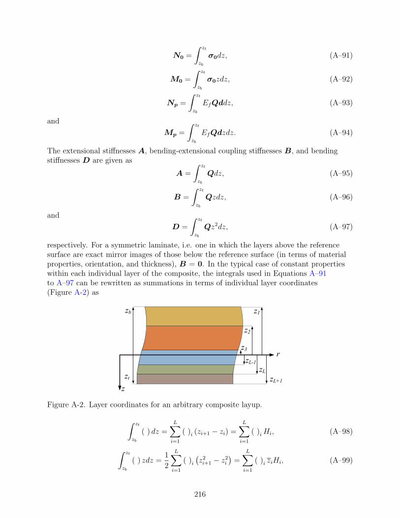
N0 =
∫ zt
zb
σ0dz, (A–91)
M0 =
∫ zt
zb
σ0zdz, (A–92)
Np =
∫ zt
zb
EfQddz, (A–93)
and
Mp =
∫ zt
zb
EfQdzdz. (A–94)
The extensional stiffnesses A, bending-extensional coupling stiffnesses B, and bendingstiffnesses D are given as
A =
∫ zt
zb
Qdz, (A–95)
B =
∫ zt
zb
Qzdz, (A–96)
and
D =
∫ zt
zb
Qz2dz, (A–97)
respectively. For a symmetric laminate, i.e. one in which the layers above the referencesurface are exact mirror images of those below the reference surface (in terms of materialproperties, orientation, and thickness), B = 0. In the typical case of constant propertieswithin each individual layer of the composite, the integrals used in Equations A–91to A–97 can be rewritten as summations in terms of individual layer coordinates(Figure A-2) as
z
r
zt zL+1
zL
z1
z2
z3
zL-1
zb
Figure A-2. Layer coordinates for an arbitrary composite layup.
∫ zt
zb
( ) dz =L∑
i=1
( )i (zi+1 − zi) =L∑
i=1
( )i Hi, (A–98)
∫ zt
zb
( ) zdz =1
2
L∑
i=1
( )i(
z2i+1 − z2i)
=L∑
i=1
( )i ziHi, (A–99)
216

and∫ zt
zb
( ) z2dz =1
3
L∑
i=1
( )i(
z3i+1 − z3i)
=L∑
i=1
( )i
(
H3i
12+ Hiz
2i
)
, (A–100)
where ( )i refers to the value of the integrand in the ith layer, Hi is the ith layer thickness,and zi is the coordinate of the center of the ith layer. Equations A–87 to A–88 are oftenwritten in a more compact form as
N
M
=
N0
M0
+
[
A B
B D
]
ε0
κ
−
Mp
Np
. (A–101)
Also, for convenience, let
N
M
=
[
A B
B D
]
ε0
κ
. (A–102)
such that the overall constitutive equation for the laminated composite becomes
N
M
=
N0
M0
+
N
M
−
Mp
Np
. (A–103)
Observing the axisymmetric assumption, Nrθ = Mrθ = 0 and the third component canbe dropped from N and M because εrθ = κrθ = 0. The various stiffness matrices thenonly need be regarded as 2×2.
A.5 Displacement Differential Equations of Motion
The axisymmetric form of the constitutive relations developed in Section A.4 maynow be combined with the axisymmetric equations of motion, Equations A–70 to A–71,to yield governing differential equations for the reference plane displacements u (r; t)and w (r; t). First, Equation A–102 is expanded to explicitly define each of the force andmoment terms,
Nr = A11
[
du
dr+
1
2
(
dw
dr
)2]
+ A12u
r− B11
d2w
dr2−B12
1
r
dw
dr, (A–104)
Nθ = A11u
r+ A12
[
du
dr+
1
2
(
dw
dr
)2]
− B111
r
dw
dr− B12
d2w
dr2, (A–105)
Mr = B11
[
du
dr+
1
2
(
dw
dr
)2]
+ B12u
r−D11
d2w
dr2−D12
1
r
dw
dr, (A–106)
and
Mθ = B11u
r+ B12
[
du
dr+
1
2
(
dw
dr
)2]
−D111
r
dw
dr−D12
d2w
dr2. (A–107)
Continuing, Equation A–70 is first solved for Nθ and then substituted into Equation A–71to yield
∂2Mr
∂r2+
2
r
∂Mr
∂r− 1
r
∂Mθ
∂r+
1
r
∂
∂r
(
rNr∂w
∂r
)
+ qz = I0w. (A–108)
217

Substituting Equations A–106 to A–107 into Equation A–108 yields
−D11∇4w + B11
[
∂3u
∂r3+
2
r
∂2u
∂r2− 1
r2∂u
∂r+
1
r3u +
(
∂2w
∂r2
)2
+∂w
∂r
∂3w
∂r3+
2
r
∂w
∂r
∂2w
∂r2
]
− B12
r
∂w
∂r
∂2w
∂r2+ ∇2 (M0 −Mp) +
1
r
∂
∂r
(
rNr∂w
∂r
)
+ qz = I0w, (A–109)
where the familiar biharmonic and Laplacian operators are defined for the axisymmetricproblem as
∇4 ( ) =1
r
d
dr
(
rd
dr
(
1
r
d
dr
(
rd ( )
dr
)))
=d4 ( )
dr4+
2
r
d3 ( )
dr3− 1
r2d2 ( )
dr2+
1
r3d ( )
dr(A–110)
and
∇2 ( ) =1
r
d
dr
(
rd ( )
dr
)
=d2 ( )
dr2+
1
r
d ( )
dr, (A–111)
respectively. Similarly, taking 1r∂[r()]∂r
of Equation A–70 and then substituting in for Nr andNθ using Equations A–104 to A–105 yields
−B11∇4w + A11
[
∂3u
∂r3+
2
r
∂2u
∂r2− 1
r2∂u
∂r+
1
r3u +
(
∂2w
∂r2
)2
+∂w
∂r
∂3w
∂r3+
2
r
∂w
∂r
∂2w
∂r2
]
− A12
r
∂w
∂r
∂2w
∂r2+ ∇2 (N0 −Np) = 0. (A–112)
Clearly both Equations A–112 and A–109 have very similar forms. Multiplying Equation A–112by B11/A11 and subtracting Equation A–109 from the result gives the governing equationfor w,
I0w +D∗11∇4w = qz −B∗
12
1
r
∂w
∂r
∂2w
∂r2+
1
r
∂
∂r
(
rNr∂w
∂r
)
+∇2
[
(M0 −Mp) −B11
A11
(N0 −Np)
]
.
(A–113)where
D∗11 = D11 −
B211
A11
(A–114)
and
B∗12 = B12 −
B11A12
A11
. (A–115)
Equation A–113 contains two unknowns, w and Nr. A second equation for Nr istherefore required. To find this equation, Equation A–28 is solved for u and substituted
218

into Equation A–27 to yield
∂ε0θ∂r
+ε0θ − ε0r
r+
1
2r
(
∂w
∂r
)2
= 0. (A–116)
This is known as a compatibility condition. Inverting Equation A–102 to find ε0r and ε0θ interms of Nr, Nθ, and w and then substituting the result into Equation A–116 and dividingby r2 yields
∂2Nr
∂r2+
3
r
∂Nr
∂r= −B∗
12
(
1
r
∂3w
∂r3+
1
r2∂2w
∂r2− 1
r3∂w
∂r
)
− A211 − A2
12
A11
1
2r2
(
∂w
∂r
)2
. (A–117)
Together, Equations A–113 and A–117 are the mixed-form differential equations forthe motion of the piezoelectric composite plate. Alternatively, Equation A–112 may berearranged into a differential equation for u in terms of w,
∂3u
∂r3+
2
r
∂2u
∂r2− 1
r2∂u
∂r+
1
r3u =
B11
A11
∇4w −(
∂2w
∂r2
)2
− ∂w
∂r
∂3w
∂r3− 2
r
∂w
∂r
∂2w
∂r2
+A12
A11
1
r
∂w
∂r
∂2w
∂r2− 1
A11
∇2 (N0 −Np) (A–118)
and Nr may be substituted into Equation A–113 to give a set of governing differentialequations purely in terms of displacement.
A.6 Equations of Equilibrium
At this juncture, the focus shifts to particulars of the problem being pursued, andseveral new assumptions are made. First, the problem is restricted to the static casefor which w = 0; the partial differential equations (PDEs) therefore become ordinarydifferential equations (ODEs). Next, σ0 and Ef are restricted to be constant in any givenlayer of the composite plate, which results in N0, M0, Np, and Mp not being functions of r.Finally, the loading is restricted to a uniform pressure acting in the z-direction, i.e. qz = p.In the following two sections, these assumptions are applied to the nonlinear equations ofmotion, which are then linearized.A.6.1 Nonlinear
Under the assumptions presented in the introduction, the governing equationsbecome, with some manipulation,
D∗11∇4w = p−B∗
12
1
2r
d
dr
[
(
dw
dr
)2]
+1
r
d
dr
(
rNrdw
dr
)
, (A–119)
with
∇4 ( ) =1
r
d
dr
(
rd
dr
(
1
r
d
dr
(
rd ( )
dr
)))
. (A–120)
219

Equation A–119 is multipled by r, integrated with respect to r, and then divided by D∗11r
to yieldd3w
dr3+
1
r
d2w
dr2− 1
r2dw
dr=
pr
2D∗11
+Nr
D∗11
dw
dr− B∗
12
2r
(
dw
dr
)2
(A–121)
Writing this equation in terms of transverse rotation,
φ = −dw
dr, (A–122)
yieldsd2φ
dr2+
1
r
dφ
dr− φ
r2= − pr
2D∗11
+Nr
D∗11
φ +B∗
12
2D∗11
φ2
r(A–123)
Either of Equations A–121 or A–123 may be taken as the governing equation fortransverse reference surface displacements.
The governing equation for in-plane reference surface displacements is found fromEquation A–118, which first may be equivalently rewritten as
1
r
d
dr
(
rd
dr
(
1
r
d (ru)
dr
))
=B11
A11
∇4w − 1
r
d
dr
(
rdw
dr
d2w
dr2
)
+
(
A12
A11
− 1
)
1
2r
d
dr
[
(
dw
dr
)2]
(A–124)Substituting Equation A–122 into Equation A–124, multiplying Equation A–124 by r,integrating with respect to r, and dividing by r gives
d2u
dr2+
1
r
du
dr− u
r2= −B11
A11
(
d2φ
dr2+
1
r
dφ
dr− φ
r2
)
−(
1 − A12
A11
)
φ2
2r− φ
dφ
dr. (A–125)
Equations A–123 and A–125 are additionally linked by Nr. Substituting Equation A–122into Equation A–117 and Equation A–102 into Equation A–123 gives
d2Nr
dr2+
3
r
dNr
dr= B∗
12
(
1
r
d2φ
dr2+
1
r2dφ
dr− φ
r3
)
− A211 − A2
12
A11
φ2
2r2. (A–126)
andd2φ
dr2+
1
r
dφ
dr−(
N0 −Np
D∗11
+1
r2
)
φ = − pr
2D∗11
+φNr
D∗11
+φ2B∗
12
2rD∗11
, (A–127)
which together are the mixed-form differential equations of equilibrium. Alternatively,Equation A–125 and Equation A–127, with Nr substituted in from Equation A–102,together compose the displacement-based differential equations of equilibrium.
For convenience in future steps, let the in-plane stress parameter be defined as
k∗2 = |N0 −Np|a2
D∗11
, (A–128)
220

where a is a characteristic dimension of the plate (such as outer radius). Substituting intoEquation A–127,
d2φ
dr2+
1
r
dφ
dr−(
xk∗2
a2+
1
r2
)
φ = − pr
2D∗11
+φNr
D∗11
+φ2B∗
12
2rD∗11
, (A–129)
where x is a flag denoting the net sense of the in-plane force terms, i.e.
x = sgn(
N0 −NPr
)
. (A–130)
A.6.2 LinearIn order to linearize Equations A–125 to A–127, second order products of displacements
are neglected, including the product φNr since Nr is a function of the displacements. Inaddition, since Np is proportional to voltage, there always exists a sufficiently smallvoltage input for which Np ≪ N0, and therefore it may be neglected from the governingdifferential equation. Alternatively, for the case of small N0, both may be negligiblecompared to the remaining terms in the linearized governing differential equation. Thus,neglecting second order products of displacements and the Np term from the governingdifferential equations yields
d2u
dr2+
1
r
du
dr− u
r2= −B11
A11
(
d2φ
dr2+
1
r
dφ
dr− φ
r2
)
. (A–131)
d2Nr
dr2+
3
r
dNr
dr=
B∗12
r
(
d2φ
dr2+
1
r
dφ
dr− φ
r2
)
, (A–132)
andd2φ
dr2+
1
r
dφ
dr−(
xk∗2
a2+
1
r2
)
φ = − pr
2D∗11
, (A–133)
where k∗2 is now redefined as
k∗2 = |N0|a2
D∗11
, (A–134)
The solution of Equation A–133 takes on three forms that are dependent on its classification.It is a first-order, non-homogeneous modified Bessel equation for x > 0, a first-order,non-homogeneous Bessel equation for x < 0, and a non-homogeneous Cauchy-Eulerequation when x = 0 [199]. Equation A–133 is next substituted into Equations A–131 toA–132, giving the simplified forms
d2u
dr2+
1
r
du
dr− u
r2= −B11
A11
(
− pr
2D∗11
+ xk∗2
a2φ
)
. (A–135)
andd2Nr
dr2+
3
r
dNr
dr=
B∗12
r
(
− pr
2D∗11
+ xk∗2
a2φ
)
. (A–136)
Equation A–133 and Equations A–135 to A–136 are now sequentially coupled, in that thesolution for φ must first be obtained before the solution to Nr or u may be. In addition,
221

it is also now clear that both Equation A–135 and Equation A–136 are forms of thenon-homogeneous Cauchy-Euler equation [199].
A.7 Problem SolutionsIn this section, solutions are presented for the linear and nonlinear forms of the
equilibrium equations of the piezoelectric composite plate. The linear solution is fullyanalytical, though the equations become sufficiently cumbersome that a matrix inversionis suggested for use in determining integration coefficients. Meanwhile, the nonlinearequations are written in a convenient form for numerical solution via readily-availablemulti-point boundary value problem solvers.
The solution domain is divided into an inner and outer region and the solutions,material properties, geometric properties, etc. within a particular domain will be denotedby a superscript (1) for the inner region and (2) for the outer region. Let the arbitrarylength scale a found in the governing equations correspond to the outer radius of theregion of interest.
The boundary conditions follow from the choices given in Equations A–72 toA–74. Using the two-domain notation, the boundary conditions for the problem includesymmetry conditions at the plate center (r = 0),
φ(1) (0) = 0, (A–137)
u(1) (0) = 0, (A–138)
matching conditions at the interface between the inner and outer region (r = a(1)),
φ(1)(
a(1))
= φ(2)(
a(1))
, (A–139)
u(1)(
a(1))
= u(2)(
a(1))
, (A–140)
w(1)(
a(1))
= w(2)(
a(1))
, (A–141)
M (1)r
(
a(1))
= M (2)r
(
a(1))
, (A–142)
N (1)r
(
a(1))
= N (2)r
(
a(1))
, (A–143)
and boundary conditions on the outer radius (r = a(2))
M (1)r
(
a(2))
= −kφφ(2)(
a(2))
(A–144)
u(2)(
a(2))
= 0 (A–145)
w(2)(
a(2))
= 0 (A–146)
The compliant boundary condition of Equation A–144 effectively means both thesimply-supported (kφ = 0) and clamped (kφ = ∞) cases are available from the finalsolution.
The solutions in the coming sections make use of the Bessel functions of the first andsecond kind, Jn and Yn, respectively and the modified-Bessel functions of the first andsecond kind, In and Kn, respectively [200].
222

A.7.1 Linear
A.7.1.1 General solutionsThe general solutions to the governing linear equations of equilibrium, Equations
A–133, A–135, and A–136, are
φ (r) =
c1I1
(
k∗ r
a
)
+ c2K1
(
k∗ r
a
)
+1
2
pa2r
D∗11k
∗2, x > 0
c1r +c2r− 1
16
pr3
D∗11
, x = 0
c1J1
(
k∗ r
a
)
+ c2Y1
(
k∗ r
a
)
− 1
2
pa2r
D∗11k
∗2, x < 0,
(A–147)
u (r) =
c3r +c4r− B11
A11
[
c1I1
(
k∗ r
a
)
+ c2K1
(
k∗ r
a
)]
, x > 0
c3r +c4r
+1
16
B11
A11
pr3
D∗11
, x = 0
c3r +c4r− B11
A11
[
c1J1
(
k∗ r
a
)
+ c2Y1
(
k∗ r
a
)]
, x < 0,
(A–148)
and
w (r) =
−c1a
k∗I0
(
k∗ r
a
)
+ c2a
k∗K0
(
k∗ r
a
)
− 1
4
pa2r2
D∗11k
∗2+ c5, x > 0
−c11
2r2 − c2 ln (r) +
1
64
pr4
D∗11
+ c5, x = 0
c1a
k∗J0
(
k∗ r
a
)
+ c2a
k∗Y0
(
k∗ r
a
)
+1
4
pa2r2
D∗11k
∗2+ c5, x < 0.
(A–149)
Following from these solutions are the force and moment resultants, Equation A–102,which with nonlinear terms neglected are
Nr (r) =
N0 −Np + B∗12I1
(
k∗ r
a
) 1
rc1 + B∗
12K1
(
k∗ r
a
) 1
rc2
+ (A11 + A12) c3 − (A11 − A12)1
r2c4 +
1
2(B11 + B12)
pa2
D∗11k
∗2,
x > 0
−Np + (B11 + B12) c1 − (B11 −B12)1
r2c2 + (A11 + A12) c3
− (A11 − A12)1
r2c4 −B∗
12
1
16
pr2
D∗11
,x = 0
N0 −Np + B∗12J1
(
k∗ r
a
) 1
rc1 + B∗
12Y1
(
k∗ r
a
) 1
rc2 + (A11 + A12) c3
− (A11 − A12)1
r2c4 −
1
2(B11 + B12)
pa2
D∗11k
∗2,
x < 0,
(A–150)
223

and
Mr (r) =
M0 −Mp +
[
D∗11k
∗
aI0
(
k∗ r
a
)
− (D∗11 −D∗
12) I1
(
k∗ r
a
) 1
r
]
c1
−[
D∗11k
∗
aK0
(
k∗ r
a
)
+ (D∗11 −D∗
12)K1
(
k∗ r
a
) 1
r
]
c2
+ (B11 + B12) c3 − (B11 −B12)1
r2c4 +
1
2(D11 + D12)
pa2
D∗11k
∗2,
x > 0
M0 −Mp + (D11 + D12) c1 − (D11 −D12)1
r2c2 + (B11 + B12) c3
− (B11 −B12)1
r2c4 − (3D∗
11 + D∗12)
1
16
pr2
D∗11
,x = 0
M0 −Mp +
[
D∗11k
∗
aJ0
(
k∗ r
a
)
− (D∗11 −D∗
12) J1
(
k∗ r
a
) 1
r
]
c1
+
[
D∗11k
∗
aY0
(
k∗ r
a
)
− (D∗11 −D∗
12)Y1
(
k∗ r
a
) 1
r
]
c2
+ (B11 + B12) c3 − (B11 −B12)1
r2c4 −
1
2(D11 + D12)
pa2
D∗11k
∗2,
x < 0.
(A–151)A.7.1.2 Particular solutions
In total, there are 5 unknown integration constants introduced via Equations A–147to A–149: c1, c2, c3, c4, and c5. As the solution to each of these equations is sought ineither domain, there are actually a total of 10 unknown integration constants in thetwo-domain problem: c
(1)i and c
(2)i with i = 1 . . . 5. With the ten boundary conditions of
Equations A–137 to A–146, the problem is thus well-posed.Given the length of the equations introduced in Section A.7.1.1, solving for the
integration constants explicitly is a burdensome task. Instead, they are found via writingthe boundary conditions as a system of linear equations solved via matrix inversion.Before that process, though, the symmetry conditions of Equations A–137 to A–138immediately reveal that c
(1)2 = c
(1)4 = 0 because each of the terms they are associated
with in Equations A–147 to A–148 are unbounded at r = 0. This reduces the unknownintegration constants to 8 in total. After substituting the appropriate general solutions ofSection A.7.1.1 into any of the remaining boundary conditions, the result may always bewritten in the form
C(1)i
Tc(1) + f
(1)i = C
(2)i
Tc(2) + f
(2)i , (A–152)
where each C(j)i is an array which contains the coefficients of the integration constants,
c(j) contains the integration constants themselves, and f(j)i represents the collected
free terms for the ith boundary condition (i = 1, 2 . . . 8) in the jth domain (j = 1, 2).Collecting the eight equations represented by Equation A–152 into a single matrixequation gives
[
−C(1)
8x3C(2)
8x5
]
3x1
c(1)
c(2)5x1
= f (1)
8x1−f (2)
8x1. (A–153)
224

The utility of Equation A–153 is that the integration constants are found in a modularmanner that allows for the coupled solution of any inner region case (x(1) = −1, 0, 1) andany outer region case (x(2) = −1, 0, 1) simply via matrix inversion of the combined [C]matrix.
Deflection of the diaphragm occurs due to any or all of 3 inputs: initial stress,pressure, or voltage. In the case of an initially stressed diaphragm, there is an existingstatic deflection before the application of voltage or pressure. Voltage or pressure loadingleads to an additional incremental deflection which in the context of lumped elementmodeling is the quantity of interest. It is thus convenient to solve for the incrementaldeflection directly. This is made possible via dividing the array of forcing terms, f (j), intoits components parts,
f (j) = f(j)0 + f (j)
p+ f (j)
v, (A–154)
where each of f(j)0 , f (j)
p, and f (j)
vinclude only those terms relating to in-plane stress,
pressure, and voltage, respectively, with all others zero. To solve for the initial deflection
alone, replace f (j) with only the in-plane component, f(j)0 (equivalent to letting v = p =
0). To solve for the incremental deflection directly, replace the total f (j) by f (j)p
or f (j)v
for incremental deflection due to pressure and voltage, respectively. In these latter cases,the in-plane stress still affects the stiffness via its inclusion in C.
In each of the following subsections, the specific definitions of the C(j) and each ofthe components of f (j) are given for all cases. The solution of the problem is obtained byusing these expressions to assemble Equation A–153, solving for the integration constantsnumerically via matrix inversion, and then plugging the numerical values into any ofEquations A–147 to A–151 depending on the quantity of interest. The substitution part ofthe process is performed for each domain, so in the end there are two equations for each ofthe displacements and force components — corresponding to the inner and outer domain— with validity over 0 ≤ r ≤ a(1) and a(1) ≤ r ≤ a(2), respectively.
225

A.7.1.3 Inner region: tension (x(1) > 0)
C(1) =
I1(
k∗(1))
0 0
−B(1)11
A(1)11
I1(
k∗(1))
a(1) 0
− a(1)
k∗(1)I0(
k∗(1))
0 1[
D∗(1)k∗(1)I0(
k∗(1))
−(
D∗(1) −D∗(1)12
)
I1(
k∗(1))
]
1a(1)
B(1)11 + B
(1)12 0
B∗(1)12 I1
(
k∗(1))
1a(1)
A(1)11 + A
(1)12 0
0 0 00 0 00 0 0
(A–155)
f (1) =
000
M(1)0
N(1)0
000
+
12
pa(1)3
D∗(1)k∗(1)2
0
−14
pa(1)4
D∗(1)k∗(1)2
12
(
D(1)11 + D
(1)12
)
pa(1)2
D∗(1)k∗(1)2
12
(
B(1)11 + B
(1)12
)
pa(1)2
D∗(1)k∗(1)2
000
+
000
−M(1)p
−N(1)p
000
(A–156)
A.7.1.4 Inner region: x(1) = 0
C(1) =
a(1) 0 00 a(1) 0
−12a(1)
20 1
D(1)11 + D
(1)12 B
(1)11 + B
(1)12 0
B(1)11 + B
(1)12 A
(1)11 + A
(1)12 0
0 0 00 0 00 0 0
(A–157)
226

f (1) =
000
M(1)0
0000
+
− 116
pa(1)3
D∗(1)
116
B(1)11
A(1)11
pa(1)3
D∗(1)
164
pa(1)4
D∗(1)
−[
3D∗(1) + D∗(1)12
]
116
pa(1)2
D∗(1)
−B∗(1)12
116
pa(1)2
D∗(1)
000
+
000
−M(1)p
−N(1)p
000
(A–158)
A.7.1.5 Inner region: compression (x(1) < 0)
C(1) =
J1(
k∗(1))
0 0
−B(1)11
A(1)11
J1(
k∗(1))
a(1) 0
a(1)
k∗(1)J0(
k∗(1))
0 1[
D∗(1)k∗(1)J0(
k∗(1))
−(
D∗(1) −D∗(1)12
)
J1(
k∗(1))
]
1a(1)
B(1)11 + B
(1)12 0
B∗(1)12 J1
(
k∗(1))
1a(1)
A(1)11 + A
(1)12 0
0 0 00 0 00 0 0
(A–159)
f (1) =
000
M(1)0
N(1)0
000
+
−12
pa(1)3
D∗(1)k∗(1)2
014
pa(1)4
D∗(1)k∗(1)2
−12
(
D(1)11 + D
(1)12
)
pa(1)2
D∗(1)k∗(1)2
−12
(
B(1)11 + B
(1)12
)
pa(1)2
D∗(1)k∗(1)2
000
+
000
−M(1)p
−N(1)p
000
(A–160)
227

A.7.1.6 Outer region: tension (x(2) > 0)
C(2) =
I1(
k∗(2)α)
K1
(
k∗(2)α)
0 0 0
−B(2)11
A(2)11
I1(
k∗(2)α)
−B(2)11
A(2)11
K1
(
k∗(2)α)
a(1) 1/
a(1) 0
− a(2)
k∗(2) I0(
k∗(2)α)
a(2)
k∗(2)K0
(
k∗(2)α)
0 0 1D∗(2)k∗(2)
a(2) I0(
k∗(2)α)
−(
D∗(2) −D∗(2)12
)
I1(
k∗(2)α)
1a(1)
−D∗(2)k∗(2)
a(2) K0
(
k∗(2)α)
−(
D∗(2) −D∗(2)12
)
K1
(
k∗(2)α)
1a(1)
B(2)11 +B
(2)12 −
(
B(2)11 −B
(2)12
)
1a(1)2 0
−B∗(2)12 I1
(
k∗(2)α)
1a(1) −B
∗(2)12 K1
(
k∗(2)α)
1a(1) A
(2)11 +A
(2)12 −
(
A(2)11 −A
(2)12
)
1a(1)2 0
[
D∗(2)k∗(2)I0(
k∗(2))
−(
D∗(2) −D∗(2)12 − kφa
(2))
I1(
k∗(2))
]
1a(2) −
[
D∗(2)k∗(2)K0
(
k∗(2))
+(
D∗(2) −D∗(2)12 − kφa
(2))
K1
(
k∗(2))
]
1a(2) B
(2)11 +B
(2)12 −
(
B(2)11 −B
(2)12
)
1a(2)2 0
−B(2)11
A(2)11
I1(
k∗(2))
−B(2)11
A(2)11
K1
(
k∗(2))
a(2) 1/
a(2) 0
− a(2)
k∗(2) I0(
k∗(2))
a(2)
k∗(2)K0
(
k∗(2))
0 0 1
(A–161)
f (2) =
000
M(2)0
N(2)0
M(2)0
00
+
12
pa(2)2a(1)
D∗(2)k∗(2)2
0
−14pa(2)2a(1)2
D∗(2)k∗(2)2
12
(
D(2)11 + D
(2)12
)
pa(2)2
D∗(2)k∗(2)2
12
(
B(2)11 + B
(2)12
)
pa(2)2
D∗(2)k∗(2)2(
D(2)11 + D
(2)12 + kφa
(2))
12
pa(2)2
D∗(2)k∗(2)2
0
−14
pa(2)4
D∗(2)k∗(2)2
+
000
−M(2)p
−N(2)p
−M(2)p
00
(A–162)
228
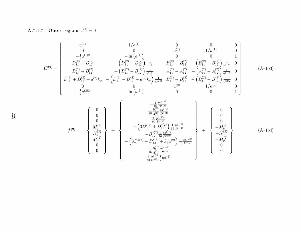
A.7.1.7 Outer region: x(2) = 0
C(2) =
a(1) 1/
a(1) 0 0 00 0 a(1) 1
/
a(1) 0−1
2a(1)2 − ln
(
a(1))
0 0 1
D(2)11 + D
(2)12 −
(
D(2)11 −D
(2)12
)
1a(1)2
B(2)11 + B
(2)12 −
(
B(2)11 − B
(2)12
)
1a(1)2
0
B(2)11 + B
(2)12 −
(
B(2)11 −B
(2)12
)
1a(1)2
A(2)11 + A
(2)12 −
(
A(2)11 − A
(2)12
)
1a(1)2
0
D(2)11 + D
(2)12 + a(2)kφ −
(
D(2)11 −D
(2)12 − a(2)kφ
)
1a(2)2
B(2)11 + B
(2)12 −
(
B(2)11 − B
(2)12
)
1a(2)2
0
0 0 a(2) 1/
a(2) 0−1
2a(2)2 − ln
(
a(2))
0 0 1
(A–163)
f (2) =
000
M(2)0
N(2)0
M(2)0
00
+
− 116
pa(1)3
D∗(2)
116
B(2)11
A(2)11
pa(1)3
D∗(2)
164
pa(1)4
D∗(2)
−(
3D∗(2) + D∗(2)12
)
116
pa(1)2
D∗(2)
−B∗(2)12
116
pa(1)2
D∗(2)
−(
3D∗(2) + D∗(2)12 + kφa
(2))
116
pa(2)2
D∗(2)
116
B(2)11
A(2)11
pa(2)3
D∗(2)
132
a(2)3
D∗(2)12pa(2)
+
000
−M(2)p
−N(2)p
−M(2)p
00
(A–164)
229

A.7.1.8 Outer region: compression (x(2) = 0)
C(2) =
J1(
k∗(2)α)
Y1
(
k∗(2)α)
0 0 0
−B(2)11
A(2)11
J1(
k∗(2)α)
−B(2)11
A(2)11
Y1
(
k∗(2)α)
a(1) 1/
a(1) 0
a(2)
k∗(2) J0(
k∗(2)α)
a(2)
k∗(2)Y0
(
k∗(2)α)
0 0 1D∗(2)k∗(2)
a(2) J0(
k∗(2)α)
−(
D∗(2) −D∗(2)12
)
J1(
k∗(2)α)
1a(1)
D∗(2)k∗(2)
a(2) Y0
(
k∗(2)α)
−(
D∗(2) −D∗(2)12
)
Y1
(
k∗(2)α)
1a(1)
B(2)11 +B
(2)12 −
(
B(2)11 −B
(2)12
)
1a(1)2 0
B∗(2)12 J1
(
k∗(2)α)
1a(1) B
∗(2)12 Y1
(
k∗(2)α)
1a(1) A
(2)11 +A
(2)12 −
(
A(2)11 −A
(2)12
)
1a(1)2 0
[
D∗(2)k∗(2)J0(
k∗(2))
−(
D∗(2) −D∗(2)12 − kφa
(2))
J1(
k∗(2))
]
1a(2)
[
D∗(2)k∗(2)Y0
(
k∗(2))
−(
D∗(2) −D∗(2)12 − kφa
(2))
Y1
(
k∗(2))
]
1a(2) B
(2)11 +B
(2)12 −
(
B(2)11 −B
(2)12
)
1a(2)2 0
−B(2)11
A(2)11
J1(
k∗(2))
−B(2)11
A(2)11
Y1
(
k∗(2))
a(2) 1/
a(2) 0
a(2)
k∗(2) J0(
k∗(2))
a(2)
k∗(2)Y0
(
k∗(2))
0 0 1
(A–165)
f (2) =
000
M(2)0
N0(2)
M(2)0
00
+
−12
pa(2)2a(1)
D∗(2)k∗(2)2
014pa(2)2a(1)2
D∗(2)k∗(2)2
−12
(
D(2)11 + D
(2)12
)
pa(2)2
D∗(2)k∗(2)2
−12
(
B(2)11 + B
(2)12
)
pa(2)2
D∗(2)k∗(2)2
−(
D(2)11 + D
(2)12 + kφa
(2))
12
pa(2)2
D∗(2)k∗(2)2
014
pa(2)4
D∗(2)k∗(2)2
+
000
−M(2)p
−N(2)p
−M(2)p
00
(A–166)
230

A.7.2 Nonlinear
In this section, the solution methodology for the nonlinear displacement-basedgoverning equations is addressed. The approach is to manipulate the governing equationsinto a form that is easily solved using existing boundary value problem solvers, forexample bvp4c or bvp5c in MATLAB [138]. A prospective solver must be capable ofsimultaneously handling the classes of singular boundary value problems (due to the 1/rterms that appears in the governing equations) and multipoint boundary value problems(due to boundary conditions applied at the interface between the inner and outer regions).Both bvp4c and bvp5c meet this criteria. They specifically solve systems of first-orderODEs of the form [138]
y′ =1
rSy + f (r,y) , (A–167)
subject to the condition thatSy (0) = 0, (A–168)
where S is a matrix of constants. The goal of this section, then, is to manipulate thenonlinear governing equations into such a form.
First, the 1/r2 singularity is removed via changing the independent variables inEquations A–125 and A–129 from φ and u to φ/r and u/r, respectively. Performing themanipulation,
d2
dr2
(
φ
r
)
+3
r
d
dr
(
φ
r
)
−(
xk∗2
a2
)
φ
r= − p
2D∗11
+Nr
D∗11
φ
r+
B∗12
2D∗11
(
φ
r
)2
(A–169)
and
d2
dr2
(u
r
)
+3
r
d
dr
(u
r
)
= −B11
A11
[(
xk∗2
a2+
Nr
D∗11
)
φ
r− p
2D∗11
+B∗
12
2D∗11
(
φ
r
)2]
−(
1 − A12
A11
)
1
2
(
φ
r
)2
−[
rd
dr
(
φ
r
)
+φ
r
]
φ
r. (A–170)
The governing equations are thus to be solved directly for φ/r and u/r, which are easilypost-processed back to φ and u.
Next, Equations A–169 to A–170 are rewritten as a series of first-order ODEs via thefollowing definitions:
y1 =φ
r, (A–171)
y3 =u
r, (A–172)
andy5 = w. (A–173)
The system of first-order ODEs is then
y′1 = y2 =d
dr
(
φ
r
)
(A–174)
231

y2′ = −3
ry2 +
(
xk∗2
a2+
Nr
D∗11
)
y1 −p
2D∗11
+B∗
12
2D∗11
y12 (A–175)
y3′ = y4 =
d
dr
(u
r
)
(A–176)
y4′ = −3
ry4 −
B11
A11
[(
xk∗2
a2+
Nr
D∗11
)
y1 −p
2D∗11
+B∗
12
2D∗11
y12
]
−(
1 − A12
A11
)
1
2y1
2 − (ry2 + y1) y1 (A–177)
y′5 =dw
dr= −φ = −ry1 (A–178)
Writing these equations explicitly in the form of Equation A–167 gives
y′1y′2y′3y′4y′5
=1
r
0 0 0 0 00 −3 0 0 00 0 0 0 00 0 0 −3 00 0 0 0 0
y1y2y3y4y5
+
y2(
xk∗2
a2+ Nr
D∗
11
)
y1 − p2D∗
11+
B∗
12
2D∗
11y1
2
y4
−B11
A11
[(
xk∗2
a2+ Nr
D∗
11
)
y1 − p2D∗
11+
B∗
12
2D∗
11y1
2]
−(
1 − A12
A11
)
12y1
2 − (ry2 + y1) y1
−ry1
.
(A–179)
To satisfy Equation A–168, it must be true that
y2 (0) =d
dr
(
φ
r
)∣
∣
∣
∣
0
= 0 (A–180)
and
y4 (0) =d
dr
(u
r
)
∣
∣
∣
∣
0
= 0. (A–181)
For proof, start by expanding y2,
y2 =1
r
dφ
dr− 1
r2φ. (A–182)
232

The second term is indeterminate at r = 0 by boundary condition A–137. ApplyingL’Hospital’s rule to this term and combining the result with the first term gives
y2 (0) =
[
1
2r
dφ
dr
]
r=0
(A–183)
Proof that Equation A–183 is true is found via application of L’Hospital’s rule toEquation A–129, which yields Equation A–183 exactly. The same analysis holds for y4(using Equation A–125 for the final step), proving that condition A–168 is satisfied.
To complete the nonlinear solution strategy, the boundary conditions must also beconsidered. It is therefore first convenient to reformulate equations for Nr and Mr in termsof the new independent variables. First, they become
Nr = xk∗2D∗11
a2+A11
[
rd
dr
(u
r
)
+u
r
]
+1
2r2(
φ
r
)2
+A12u
r+B11
[
rd
dr
(
φ
r
)
+φ
r
]
+B12φ
r
(A–184)and
Mr = M0−Mp+B11
[
rd
dr
(u
r
)
+u
r
]
+1
2r2(
φ
r
)2
+B12u
r+D11
[
rd
dr
(
φ
r
)
+φ
r
]
+D12φ
r,
(A–185)which are equivalent to the solver-friendly forms
Nr = xk∗2D∗11
a2+ A11
(
ry4 + y3 +1
2(ry1)
2
)
+ A12y3 + B11 (ry2 + y1) + B12y1 (A–186)
and
Mr = M0 −MPr + B11
(
ry4 + y3 +1
2(ry1)
2
)
+ B12y3 + D11 (ry2 + y1) + D12y1. (A–187)
233

The boundary conditions, transformed from Equations A–137 to A–146 are then
y(1)2 (0) = 0, (A–188)
y(1)4 (0) = 0, (A–189)
y(1)1
(
a(1))
= y(2)1
(
a(1))
, (A–190)
y(1)3
(
a(1))
= y(2)3
(
a(1))
, (A–191)
y(1)5
(
a(1))
= y(2)5
(
a(1))
, (A–192)
M (1)r
(
a(1))
= M (2)r
(
a(1))
, (A–193)
N (1)r
(
a(1))
= M (2)r
(
a(1))
, (A–194)
M (2)r
(
a(2))
= −kφry(2)1
(
a(2))
, (A–195)
y(2)3
(
a(2))
= 0, and (A–196)
y(2)5
(
a(2))
= 0. (A–197)
This completes the solution strategy for the nonlinear governing differential equations.Note that boundary value problem solvers are of course also capable of solving lineardifferential equations, and in fact a straightforward way of solving the linear problem is toprogram a variant of the solution presented in this section with nonlinear terms removed.
A.8 Closing
In this appendix, solution procedures for both the linear and nonlinear problem of aan axisymmetric, laminated, pre-stressed, and radially-discontinuous circular piezoelectricplate exposed to pressure and/or voltage loading were presented. These linear solution isutilized to provide inputs to the lumped element model in Chapter 5, while the nonlinearsolution is used to form a constraint in the optimization of Chapter 6. The models arevalidated against finite element analysis in Section 5.2.5.
234

APPENDIX BBOUNDARY CONDITION INVESTIGATION
This appendix briefly describes an investigation of the outer boundary condition (atr = a2) used in the diaphragm model. The clamped boundary condition utilized in themodel development of Appendix A and also in the validation exercise of Section 5.2.5.1is an idealization that does not take into account the compliance of the substrate. Afinite element model that includes the substrate is developed here to compare to thefinite element simulation completed in Section 5.2.5.1, which utilized a clamped boundarycondition.
@@RFixed BC
@@RRoller BC
Piezoelectric film stack
Silicon substrate
RPressure loading
A
B
Figure B-1. Finite element model for investigation of boundary compliancy. A) Boundarygeometry with boundary conditions. B) Mesh.
A finite element model that includes a section of the silicon substrate — with thesubstrate reduced here to 60µm × 30µm because stress is concentrated in the surfaceregion — is pictured in Figure B-1. Boundary conditions, which include a fixed boundarycondition on the bottom of the substrate and a roller boundary condition on the far rightside, are shown in Figure B-1A. The displacement profiles were found for a pressureloading along the entire top surface of the model. All other conditions, including thoseinvolving the piezoelectric film stack and stress, are retained from Section 5.2.5.1.
The linear mode shapes predicted from the finite element models with both clampedand compliant boundaries are found in Figure B-2 for an applied pressure of 111 dB.
235

Agreement is very good; when integrated, the total difference in volume displacement ∆∀is less than 1%. This indicates that at least for the geometry used in this model (designD), compliant boundary conditions aren’t likely to be a large contributor to error in linearmodel predictions.
0 50 100 150 200 250 3000
0.5
1
1.5
Radial coordinate [µm]
win
c(0
)[n
m]
Clamped BC
Compliant BC
Figure B-2. Deflection profiles from FEA with clamped and compliant boundaryconditions (P=111 dB).
Figure B-3A shows a comparison between the incremental deflection at r = 0 foundfrom the finite element model with a clamped outer boundary condition (Section 5.2.5.1)and that found from the finite element model with substrate. The two agree extremelyclosely over much of the interval. A plot of the relative error between the two sets ofsimulation results is found in Figure B-3B, which shows that the compliance in theboundary conditions becomes more important at high pressure levels. The relative error isbelow 5.5% up to 172 dB, with a maximum of 11.4% at 190 dB.
100 120 140 160 180
10−3
10−1
101
Pressure [dB re 20µPa]
win
c(0
)[µ
m] Clamped BC
Compliant BC
A
100 120 140 160 1800
5
10
15
Pressure [dB re 20µPa]
Rel
.E
rror
inw
inc(0
)[%
]
B
Figure B-3. FEA results for models with clamped and compliant boundary conditions(versus pressure). A) Incremental center deflection. B) Relative error.
236

APPENDIX CUNCERTAINTY ANALYSIS
This appendix addresses the calculation of uncertainty estimates for measuredquantities in Chapter 8.
C.1 ApproachThe general approach to uncertainty estimation to be used here is consistent with the
methodology presented in Coleman & Steele [201], which is drawn from the ISO standard[202]. In each case, the combined standard uncertainty for a random variable is first foundvia the root sum square method
u =
√
√
√
√s2 +M∑
k=1
b2k, (C–1)
where s is the standard deviation estimate for the random uncertainty and bk is thestandard deviation estimate for the kth systematic uncertainty (bias). Note that the useof Equation C–1 requires that error sources are uncorrelated. The confidence bounds arethen determined using a coverage factor via
U% = t%u, (C–2)
where t% is the t-statistic with ν degrees of freedom associated with a selected confidencelevel in percent. The t-statistic may be drawn from standard tables [34, 163, 201] or fromMATLAB as tinv(1-α/2,ν) for the (1 − α) × 100% confidence bound. The degrees offreedom ν in the presence of bias errors can be estimated from the Welch-Satterthwaiteformula [201]. The statistic t95% is typically taken as 2 for ν > 30, which is often the casewhen bias errors are well-defined and a large number of measurements (N = ν + 1 > 31)were taken. This assumption will be made throughout the uncertainty analysis presentedin the following sections. In the case of uncertainty in a result calculated from severalvariables, the Taylor Series Method (TSM) is employed [201]. The combined standarduncertainty for a function r = r (x1, x2, . . . , xn) is given as [201]
ur2 =
J∑
i=1
(
∂r
∂xi
)2
b2xi+
J∑
i=1
(
∂r
∂xi
)2
s2xi, (C–3)
where bxiand sxi
are associated with the ith variable.The uncertainty estimation approach discussed here requires some knowledge of
the statistical properties of bias errors. In the absence of data, a distribution must beassumed. In the sections to follow, a bias error of ±a is typically drawn from a uniformdistribution, yielding a standard deviation estimate of a/
√3.
Error estimates for spectral quantities [34] used repeatedly include the normalizedstandard errors of autospectral density,
sGxx
Gxx
=1
√ndeff
, (C–4)
237

frequency response function magnitude,
s|Hxy |
|Hxy (f)| =
√
1 − γ2xy (f)
|γxy (f)|√2ndeff
, (C–5)
and phase (in radians),
sφxy=
√
1 − γ2xy (f)
|γxy (f)|√2ndeff
, (C–6)
where ndeff is the effective number of averages and γ2xy is the ordinary coherence function.
For a rectangular window with 0 % overlap, ndeff = nd, the actual number of averages. Foran arbitrarily windowed measurement with overlap,
nd = ⌊1 + (bblocks − 1) / (1 − r)⌋, (C–7)
where bblocks is the number of blocks and r is the fraction of overlap. The effective numberof averages depends on both the window and the overlap as [203]
ndeff = λnd, (C–8)
where for the Hanning window with 75 % overlap (r = 0.75), λ = 0.52. The concept of theeffective number of averages — with different nomenclature — was addressed by Welch[204].
C.2 Frequency Response FunctionThis section addresses the uncertainty estimates for frequency response functions of
the developed microphones, for instance as presented in Section 8.2.3.1.The PULSE software only enables specification of the pistonphone pressure level
(which is corrected for atmospheric pressure) up to the nearest 0.1 dB SPL; this impliesa bias error of up to ±0.05 dB propagates into the DUT frequency response function.Drawing the bias error from a uniform distribution over ±0.05 dB, the standard bias errorestimate is
b|Hxy | =100.05/20 − 1√
3|Hxy (f)| (C–9)
≈ 0.0033 |Hxy (f)| .
The standard deviation estimate for the random uncertainty is found from Equation C–5and U95% is calculated from Equations C–1 to C–2 with t95% = 2 since 100 averages weretaken in all frequency microphone frequency response measurements.
C.3 Noise FloorThis section addresses uncertainty for noise floor measurements presented in
Section 8.2.4.1. Uncertainty for minimum detectable pressure metrics calculated fromnoise floor measurements are also given.
238

C.3.1 Spectra
The random uncertainty of the noise floor measurement was estimated usingEquation C–4 for power spectral density, taking into account the different numbers ofblocks collected over each frequency span, the 75 % overlap, and Hanning window via theprocedure addressed in the opening. The 95 % confidence interval is then
U95% = 2sSvo
(C–10)
= 2Svo√
ndeff
. (C–11)
Letting U95% = U95%/Svo , the generally unsymmetric ± error bounds in dB can be
determined as 10 log10
(
1 + U95%
)
and −10 log10
(
1 − U95%
)
, respectively. Subtracting the
two bounds gives 10 log10
(
1 − U95%
)
and one sees that the asymmetry is not important
when U295% ≪ 1. The uncertainty for each span is shown graphically in Figure C-1.
0 6.4 12.8 25.6 38.4 51.2 76.8 102.4
0.19 0.19 0.08 0.08 0.06 0.06 0.06
f [kHz]
±U95% [dB]
Figure C-1. Noise spectra 95% confidence intervals.
The standard combined uncertainty of the minimum detectable pressure spectraaccounting for the uncertainty in both the noise floor and microphone sensitivities wasestimated using the TSM as
u2MDP =
(
∂MDP
∂Svo
)2
sSvo
+
(
∂MDP
∂ |S|
)2
u2|S|, (C–12)
which after performing the partial differentiations and normalizing gives
u2MDP
MDP2 =
(
1
2
sSvo
Svo
)2
+
(
u|S|
|S|
)2
. (C–13)
Note the use of the combined standard error for |S|, which accounts for both random andbias error in the individual microphone sensitivities. The uncertainties are the same for allmicrophones and are shown for each frequency span in Figure C-2.
0 6.4 12.8 25.6 38.4 51.2 76.8 102.4
0.10 0.10 0.05 0.05 0.04 0.04 0.04
f [kHz]
±U95% [dB]
Figure C-2. MDP spectra 95% confidence intervals.
239

C.3.2 Narrow Band
The expression of the 95% confidence interval of the narrow band MDP is unchangedfrom Equation C–13. It is simply the uncertainty value for the MDP spectrum at 1 kHz,U95% = ±0.19 dB.C.3.3 Integrated
Uncertainty of the integrated MDP measures, in OASPL and AOASPL, requiredcomplex integration processes and were therefore obtained via Monte Carlo simulations.Random perturbations of the minimum detectable pressure spectra were taken from anormal distribution with a standard deviation equal to the combined standard uncertaintyupmin
(= 20µPa10uMDP
20 ) defined in Section C.3.1. The two integration processes wereperformed on 5000 randomly perturbed spectra, which yielded converged statistics.Calculation of U95% from Monte Carlo results via t95%u and also from an empiricalcumulative distribution function agreed to at least the number of decimal places reportedin Table 8-14 for all designs.
C.4 ImpedanceImpedance measurement results were given in Section 8.2.4.2. The kth impedance
measurement from the HP 4294A impedance analyzer post-processed into admittanceform is written as
Yk (f) = Gk (f) + jBk (f) . (C–14)
From n total measurements, the mean values G and B were computed, together withtheir sample standard deviations, sG = sG/
√n and sB = sB/
√n. Five thousand Monte
Carlo simulations were used to fit the data to Equation 8–7, with perturbations to Gand B and a curve fit performed at each iteration. The perturbations representing therandom error were drawn from a normal distribution (mean zero and standard deviationsG and sB, respectively), and those representing the bias error were drawn from a uniformdistribution with bounds equal to the bias error, calculable from expressions in theequipment manual [175]. The extracted values Cef + Ceo, Rep, and Res were saved at eachiteration together with R-squared values for the goodness of fit to the experimental data,yielding statistical distributions for all of those quantities. From those, the 95% confidencebounds were extracted directly from an experimental cumulative distribution function.
C.5 Parasitic Capacitance Extraction
The TSM was applied to Equation 8–12 to yield the combined standard uncertaintyexpression,
u2Cep+Cea
= (Cet)2
[
u2Sca
+ b2Sca
S2ca
+u2Sva
+ b2Sva
S2va
+s2Cfb
C2fb
]
+ u2Cef
, (C–15)
which because Sca = Sca (f) and Sva = Sva (f), is evaluated at each frequency. The errorsused in Equation C–15 are found in Table C-1. Similarly, the uncertainty in the opencircuit sensitivity was estimated from
u2Soc
=
(
Cet
Cef
)2(
s2Sva+ b2Sva
)
+
(
Cep + Cea
C2ef
Sva
)2
u2Cef
+
(
Sva
Cef
)2
u2Cep+Cea
. (C–16)
In both cases, U95% = 2u.
240
Table C-1. Parasitic capacitance extraction uncertainties.
Uncertainty Value
sScaEquation C–5
bSca0.0033Sca (see Equation C–9)
sSvaEquation C–5
bSva0.0033Sva (see Equation C–9)
sCfb±0.25 pF
C.6 Parameter ExtractionUncertainty estimates for the primary parameter extraction quantities found in
Section 8.2.5, Cad, Mad, and da, were obtained via Monte Carlo simulations. The spatialfrequency response functions from which they were calculated, Hpw(r, θ; f) and Hvw(r, θ; f)contained random error (defined by Equation C–5) and bias error from the microphonecalibration in the case of Hpw (defined via the general form of Equation C–9). The biaserror associated with the actual laser vibrometer measurement was deemed negligible.The perturbations representing the random error were drawn from a normal distribution,with each individual scan point perturbed individually. Perturbations associated with thebias error were drawn from a uniform distribution and applied uniformly to each scanpoint. The integration routines associated with the calculation of Cad, Mad and da wereperformed for each perturbation to build statistical distributions and U95% for each wascalculated directly from the experimental cumulative probability distribution function.
Secondary parameters φa and k were calculated via the below equations using thestandard uncertainties derived from the Monte Carlo simulations:
(
uφa
φa
)2
=
(
uda
da
)2
+
(
uCad
Cad
)2
(C–17)
and(uk2
k2
)2
=
(
2uda
da
)2
+
(
uCef
Cef
)2
+
(
uCad
Cad
)2
. (C–18)
Uncertainty in Cef in the above equation was drawn from Table 8.2.4.2.
241
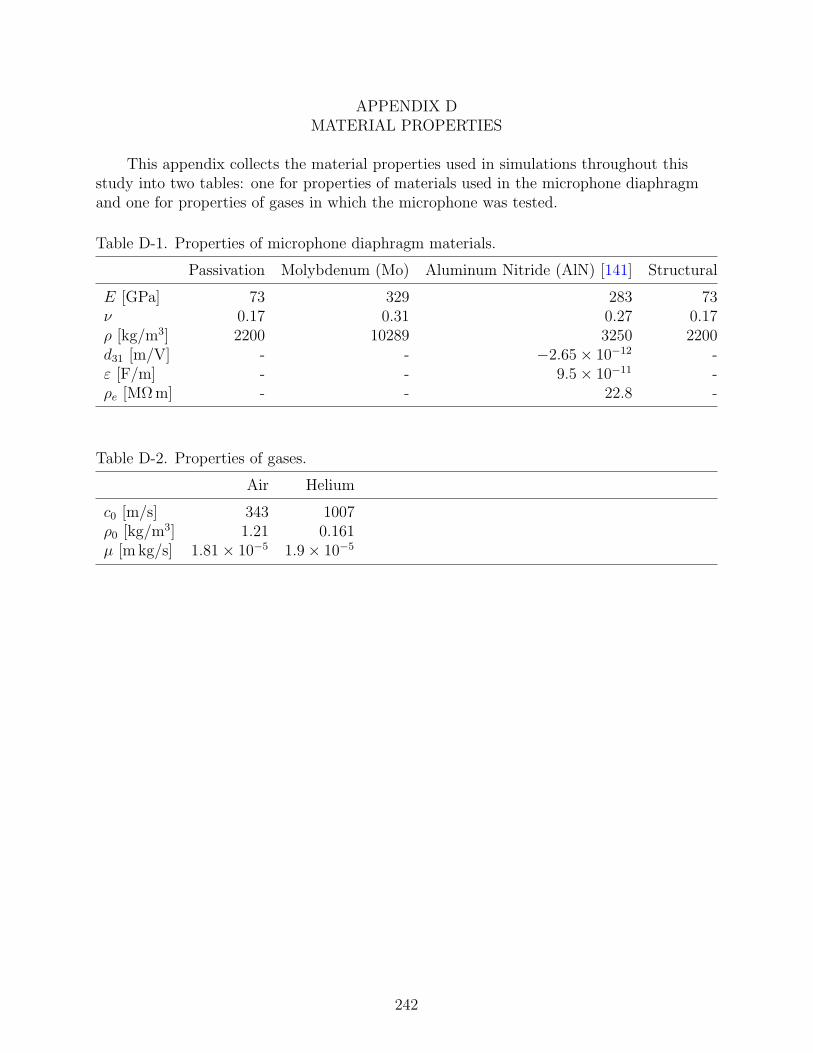
APPENDIX DMATERIAL PROPERTIES
This appendix collects the material properties used in simulations throughout thisstudy into two tables: one for properties of materials used in the microphone diaphragmand one for properties of gases in which the microphone was tested.
Table D-1. Properties of microphone diaphragm materials.
Passivation Molybdenum (Mo) Aluminum Nitride (AlN) [141] Structural
E [GPa] 73 329 283 73ν 0.17 0.31 0.27 0.17ρ [kg/m3] 2200 10289 3250 2200d31 [m/V] - - −2.65 × 10⁻¹² -ε [F/m] - - 9.5 × 10⁻¹¹ -ρe [MΩ m] - - 22.8 -
Table D-2. Properties of gases.
Air Helium
c0 [m/s] 343 1007ρ0 [kg/m3] 1.21 0.161µ [m kg/s] 1.81 × 10⁻⁵ 1.9 × 10⁻⁵
242
REFERENCES
[1] B. Burnett, “Ssshh, we’re flying a plane around here,” Boeing Frontiers, vol. 4,no. 8, Jan. 2006.
[2] P. A. Sheikh and C. Uhl, “Airplane noise: A pervasive disturbance in Pennsylvaniaparks, USA,” Journal of Sound and Vibration, vol. 274, no. 1-2, pp. 411–420, Jul.2004. [Online]. Available: http://dx.doi.org/10.1016/j.jsv.2003.09.014
[3] “Aeronautics and space, noise standards: Aircraft type and airworthinesscertification,” Title 14 US Code of Federal Regulations, pt. 36, 2004.
[4] V. G. Mengle, U. Ganz, E. J. Bultemeier, and F. T. Calkins, “Clocking effectsof chevrons with azimuthally-varying immersions on shockcell/cabin noise,” inProceedings of the 29th AIAA Aeroacoustics Conference, Vancouver, Canada, May5–7, 2008, AIAA paper 08-3000, pp. 1–14.
[5] Occupational safety and health protections for cabin crew members, InternationalCivil Aviation Organization Working Paper, Rev. A36-WP/208, Sep. 2007.
[6] W. H. Herkes, R. F. Olsen, and S. Uellenberg, “The quiet technology demonstratorprogram : Flight validation of airplane noise-reduction concepts,” in Proceedingsof the 12th AIAA/CEAS Aeroacoustics Conference (27th Aeroacoustics Conference),Cambridge, MA, May 8–10, 2006, AIAA paper 2006-2720, pp. 1–9.
[7] E. J. Bultemeier, U. Ganz, J. Premo, and E. Nesbitt, “Effect of uniform chevronson cruise shockcell noise,” in Proceedings of the 12th AIAA/CEAS AeroacousticsConference (27th AIAA Aeroacoustics Conference), Cambridge, MA, May 8–10, 2006,AIAA paper 2006-2440, pp. 1–15.
[8] D. Reed, S. Uellenberg, and E. Davis, “An in-flight study of cabin buzz-saw noise,”The Journal of the Acoustical Society of America, vol. 112, no. 5, pp. 2347–2347,2002. [Online]. Available: http://link.aip.org/link/?JAS/112/2347/2
[9] W. Herkes, E. Nesbitt, B. Callender, B. Janardan, J. Moe, and J. Yu, “The quiettechnology demonstrator program : Static test of airplane noise-reduction concepts,”in Proceedings of the 13th AIAA/CEAS Aeroacoustics Conference (28th AIAAAeroacoustics Conference), Rome, Italy, May 21–23, 2007, AIAA paper 2007-3670,pp. 1–11.
[10] S. Bailey, G. Kunkel, M. Hultmark, M. Vallikivi, J. Hill, K. Meyer, C. Tsay,C. Arnold, and A. Smits, “Turbulence measurements using a nanoscale thermalanemometry probe,” Journal of Fluid Mechanics, vol. 663, pp. 160–179, Nov. 2010.[Online]. Available: http://dx.doi.org/10.1017/S0022112010003447
[11] J. W. Naughton and M. Sheplak, “Modern developments in shear-stress measurement,”Progress in Aerospace Sciences, vol. 38, no. 6–7, pp. 515–570, Aug.–Oct. 2002.[Online]. Available: http://dx.doi.org/10.1016/S0376-0421(02)00031-3
243

[12] H. Tennekes and J. Lumley, A first course in turbulence. Cambridge, MA: MITPress, 1972.
[13] L. Lofdahl and M. Gad-el-Hak, “MEMS-based pressure and shear stress sensors forturbulent flows,” Measurement Science and Technology, vol. 10, no. 8, p. 665, Aug.1999. [Online]. Available: http://stacks.iop.org/0957-0233/10/i=8/a=302
[14] T. J. Mueller, Ed., Aeroacoustic Measurements. Berlin, Germany: Springer-Verlag,2002, ch. 3, pp. 98–217.
[15] D. P. Arnold, T. Nishida, L. N. Cattafesta, and M. Sheplak, “A directionalacoustic array using silicon micromachined piezoresistive microphones,” Journal ofthe Acoustical Society of America, vol. 113, no. 1, pp. 289–298, Jan. 2003. [Online].Available: http://dx.doi.org/10.1121/1.1527960
[16] M. Sheplak, K. S. Breuer, and M. A. Schmidt, “A wafer-bonded, silicon-nitridemembrane microphone with dielectrically-isolated single crystal silicon piezoresistors,”in Proceedings of 1998 Solid-State Sensor and Actuator Workshop, Hilton HeadIsland, SC, Jun. 8–11, 1998, pp. 23–26.
[17] M. Sheplak, M. Seiner, K. S. Breuer, and M. A. Schmidt, “A MEMS microphonefor aeroacoustic measurements,” in Proceedings of 37th AIAA Aerospace SciencesMeeting, Reno, NV, Jan. 11–14, 1999, AIAA paper 99-0606.
[18] D. P. Arnold, S. Gururaj, S. Bhardwaj, T. Nishida, and M. Sheplak, “A piezoresistivemicrophone for aeroacoustic measurements,” in Proceedings of ASME IMECE 2001International Mechanical Engineering Congress and Exposition, New York, NY, Nov.11–16, 2001, paper MEMS-23841, pp. 281–288.
[19] P. J. King and J. R. Underbrink, “Characterization of a microelectromechanicalsystems (MEMS) microphone,” in Proceedings of the 14th AIAA/CEAS AeroacousticsConference, Vancouver, Canada, May 5–7, 2008, AIAA paper 2008-2912.
[20] S. Horowitz, T. Nishida, L. Cattafesta, and M. Sheplak, “Development of amicromachined piezoelectric microphone for aeroacoustics applications,” Journal ofthe Acoustical Society of America, vol. 122, no. 6, pp. 3428–3436, Dec. 2007. [Online].Available: http://dx.doi.org/10.1121/1.2785040
[21] D. Martin, “Design, fabrication, and characterization of a MEMS dual-backplatecapacitive microphone,” Ph.D. dissertation, University of Florida, Gainesville, FL,Aug. 2007. [Online]. Available: http://purl.fcla.edu/fcla/etd/UFE0017526
[22] V. G. Mengle, U. Ganz, E. Nesbitt, E. J. Bultemeier, and R. Thomas, “Flight testresults for uniquely tailored propulsion-airframe aeroacoustic chevrons: Shockcellnoise,” in Proceedings of the 27th AIAA Aeroacoustics Conference, Cambridge, MA,May 5–7, 2008, AIAA paper 08-3000.
244

[23] P. Sijtsma and R. Stoker, “Determination of absolute contributions of aircraftnoise components using fly-over array measurements,” in Proceedings of the 10thAIAA/CEAS Aeroacoustics Conference, Manchester, Great Britain, May 10–12, 2004,AIAA paper 2004-2958.
[24] H. Siller, M. Drescher, G. Saueressig, and R. Lange, “Fly-over source localisation ona Boeing 747-400,” in Proceedings of the 3rd Berlin Beamforming Conference, Berlin,Germany, Feb. 24–25, 2010, pp. 1–11.
[25] K. Veggeberg, “High channel-count aircraft noise mapping applications,” Sound andVibration Magazine, pp. 14–16, May 2009.
[26] J. Lan, J. Premo, G. Zlavog, C. Breard, B. Callender, and M. Martinez, “Phased arraymeasurements of full-scale engine inlet noise,” in Proceedings of the 13th AIAA/CEASAeroacoustics Conference (28th AIAA Aeroacoustics Conference), Rome, Italy, May21–23, 2007, AIAA paper 2007-3434, pp. 1–14.
[27] L. Brusniak, J. R. Underbrink, E. Nesbitt, D. Lynch, and M. Martinez, “Phasedarray measurements of full-scale engine exhaust noise,” in Proceedings of the 13thAIAA/CEAS Aeroacoustics Conference (28th AIAA Aeroacoustics Conference),Rome, Italy, May 21–23, 2007, AIAA paper 2007-3612, pp. 1–18.
[28] D. T. Blackstock, Fundamentals of Physical Acoustics. New York, NY: John Wiley& Sons, Inc, 2000, ch. 1,4,14.
[29] J. E. F. Williams, “Hydrodynamic noise,” Annual Review of FluidMechanics, vol. 1, no. 1, pp. 197–222, Jan. 1969. [Online]. Available:http://dx.doi.org/10.1146/annurev.fl.01.010169.001213
[30] M. Lighthill, “Sound generated aerodynamically,” Philosophical Transactions of theRoyal Society A: Mathematical, Physical and Engineering Sciences, vol. 267, no. 1329,pp. 147–182, Jun. 1961. [Online]. Available: http://www.jstor.org/stable/2414246
[31] Microphone Handbook, Bruel and Kjær, Nærum, Denmark, Jul. 1996. [Online].Available: http://www.bksv.com/doc/be1447.pdf
[32] H. H. Hubbard, “Aeroacoustics of flight vehicles: theory and practice,” NationalAeronautics and Space Administration, Tech. Rep. 90-3052, 1991.
[33] C. M. Harris, Handbook of Acoustical Measurements and Noise Control, 3rd ed.Woodbury, NY: Acoustical Society of America, 1998, ch. 1.
[34] J. S. Bendat and A. G. Piersol, Random Data Analysis and Measurement Procedures,3rd ed. New York, NY: John Wiley and Sons, 2000, ch. 2,6,9.
[35] M. Rossi, Acoustics and Electroacoustics. Norwood, MA: Artech House, Inc., 1988,ch. 4–6,8.
245
[36] L. L. Beranek, Acoustics. New York, NY: Acoustical Society of America, 1993, ch.3,5,6.
[37] S. S. Rao, Vibration of Continuous Systems. Hoboken, N.J.: Wiley, 2007, ch. 14.
[38] R. Dieme, G. Bosman, M. Sheplak, and T. Nishida, “Source of excessnoise in silicon piezoresistive microphones,” Journal of the Acoustical Societyof America, vol. 119, no. 5, pp. 2710–2720, May 2006. [Online]. Available:http://dx.doi.org/10.1121/1.2188367
[39] C. Motchenbacher and J. Connelly, Low Noise Electronic System Design. New York,NY: John Wiley & Sons, 1993, ch. 1,2.
[40] T. B. Gabrielson, “Mechanical-thermal noise in micromachined acoustic and vibrationsensors,” IEEE Transactions on Electron Devices, vol. 40, no. 5, pp. 903–909, May1993. [Online]. Available: http://dx.doi.org/10.1109/16.210197
[41] H. B. Callen and T. A. Welton, “Irreversibility and generalized noise,”Physical Review, vol. 83, no. 1, pp. 34–40, Jul. 1951. [Online]. Available:http://dx.doi.org/10.1103/PhysRev.83.34
[42] T. B. Gabrielson, “Fundamental noise limits for miniature acoustic and vibrationsensors,” Journal of Vibration and Acoustics, vol. 117, no. 4, pp. 405–410, Oct. 1995.[Online]. Available: http://dx.doi.org/10.1115/1.2874471
[43] S. D. Senturia, Microsystem Design. Norwell, MA: Kluwer Academic Publishers,2001, ch. 1,2,5,13,16.
[44] LTC6240/LTC6241/LTC6242 Single/Dual/Quad 18 MHz, Low Noise, Rail-to-RailOutput, CMOS Op Amps, Linear Technology, 2011.
[45] G. Vasilescu, Electronic Noise and Interfering Signals: Principles and Applications.Berlin, Germany: Springer, 2005, ch. 1.
[46] P. Horowitz and W. Hill, The Art of Electronics, 2nd ed. Cambridge, UK: CambridgeUniversity Press, 1989, ch. 7.
[47] B. Boulet, Fundamentals of Signals and Systems. Hingham, MA: Da VinciEngineering Press, 2006, vol. 1, ch. 4.
[48] Audio Distortion Measurements, Bruel and Kjær, Nærum, Denmark, 1992. [Online].Available: http://www.bksv.com/doc/BO0385.pdf
[49] Measurement Microphones, 2nd ed., Bruel and Kjær, Nærum, Denmark, Aug. 1994.[Online]. Available: http://www.bksv.com/doc/br0567.pdf
[50] 1/8 in Pressure-Field Microphone - Type 4138, Bruel and Kjær, Sep. 2008.
[51] 1/4 in Pressure-Field Microphone - Type 4938, Bruel and Kjær, May 2008.
246

[52] Kulite High Intensity Microphones, Kulite, Feb. 2011. [Online]. Available:http://www.kulite.com/pdfs/pdf Data Sheets/Mic.pdf
[53] P. R. Scheeper, A. G. H. van der Donk, W. Olthuis, and P. Bergveld, “A review ofsilicon microphones,” Sensors and Actuators A, vol. 44, no. 1, pp. 1–11, Jul. 1994.[Online]. Available: http://dx.doi.org/10.1016/0924-4247(94)00790-X
[54] B. Homeijer, “Design, fabrication and characterization of a MEMS piezoresistivemicrophone for use in aeroacoustic measurements,” Ph.D. dissertation,University of Florida, Gainesville, FL, Dec. 2008. [Online]. Available:http://purl.fcla.edu/fcla/etd/UFE0022840
[55] M. Royer, J. O. Holmen, M. A. Wurm, O. S. Aadland, and M. Glenn, “ZnO on Siintegrated acoustic sensor,” Sensors and Actuators, vol. 4, no. 3, pp. 357–362, 1983.[Online]. Available: http://dx.doi.org/10.1016/0250-6874(83)85044-6
[56] E. S. Kim and R. S. Muller, “IC-processed piezoelectric microphone,” IEEEElectron Device Letters, vol. 8, no. 10, pp. 467–468, Oct. 1987. [Online]. Available:http://dx.doi.org/10.1109/EDL.1987.26696
[57] R. S. Muller and E. S. Kim, “IC processed piezoelectric microphone,” U.S. Patent4 783 821, Nov. 8, 1988.
[58] E. S. Kim, R. S. Muller, and P. R. Gray, “Integrated microphone with CMOScircuits on a single chip,” in Proceedings of 1989 International Electron DevicesMeeting, Washington, DC, Dec. 3–6, 1989, pp. 880–883. [Online]. Available:http://dx.doi.org/10.1109/IEDM.1989.74193
[59] E. S. Kim, J. R. Kim, and R. S. Muller, “Improved IC-compatible piezoelectricmicrophone and CMOS process,” in Proceedings of 1991 International Conferenceon Solid-State Sensors and Actuators, San Francisco, CA, Jun. 24–27, 1991, pp.270–273. [Online]. Available: http://dx.doi.org/10.1109/SENSOR.1991.148858
[60] J. Franz, “Piezoelektrische sensoren auf siliziumbasis fur akustische anwendungen,”Ph.D. dissertation, Darmstadt University of Technology, Darmstadt, Germany, 1988.
[61] R. Schellin, G. Hess, W. Kuehnel, G. M. Sessler, and E. Fukada, “Siliconsubminiature microphones with organic piezoelectric layers: Fabricationand acoustical behaviour,” in Proceedings of 7th International Symposium onElectrets, Berlin, Germany, Sep. 25–27, 1992, pp. 929–934. [Online]. Available:http://dx.doi.org/10.1109/ISE.1991.167338
[62] R. Schellin, G. Hess, R. Kressmann, and P. Wassmuth, “Micromachinedsilicon subminiature microphones with piezoelectric P(VDF/TRFE)-layers andsilicon-nitride-membranes,” in Proceedings of 8th International Symposium onElectrets, Paris, France, Sep. 7–9, 1994, pp. 1004–1009. [Online]. Available:http://dx.doi.org/10.1109/ISE.1994.515262
247

[63] R. P. Ried, E. S. Kim, D. M. Hong, and R. S. Muller, “Piezoelectric microphone withon-chip CMOS circuits,” Journal of Microelectromechanical Systems, vol. 2, no. 3,pp. 111–120, Sep. 1993. [Online]. Available: http://dx.doi.org/10.1109/84.260255
[64] S. S. Lee, R. P. Reid, and R. M. White, “Piezoelectric cantilever microphone andmicrospeaker,” Journal of Microelectromechanical Systems, vol. 5, no. 4, pp. 238–242,Dec. 1996. [Online]. Available: http://dx.doi.org/10.1109/84.546403
[65] S. S. Lee and R. M. White, “Piezoelectric cantilever acoustic transducer,” Journalof Micromechanics and Microengineering, vol. 8, no. 3, pp. 230–238, 1998. [Online].Available: http://dx.doi.org/10.1088/0960-1317/8/3/009
[66] A. Naguib, E. Soupos, H. Nagib, C. Huang, and K. Najafi, “Characterization of aMEMS acoustic/pressure sensor,” in Proceedings of 37th AIAA Aerospace SciencesMeeting, Reno, NV, Jan. 11–14, 1999, AIAA paper 99-0520, pp. 1–7.
[67] ——, “A piezoresistive MEMS sensor for acoustic noise measurements,” in Proceedingsof 5th AIAA/CEAS Aeroacoustics Conference & Exhibit, Bellevue, WA, May 10–12,1999, AIAA paper 99-1992, pp. 1–8.
[68] C. Huang, A. Naguib, E. Soupos, and K. Najafi, “A silicon micromachinedmicrophone for fluid mechanics research,” Journal of Micromechanics andMicroengineering, vol. 12, no. 6, pp. 767–774, Nov. 2002. [Online]. Available:http://dx.doi.org/10.1088/0960-1317/12/6/307
[69] D. P. Arnold, “A MEMS-based directional acoustic array for aeroacousticmeasurements,” Master’s thesis, University of Florida, Gainesville, FL, Dec. 2001.
[70] K. Kadirvel, R. Taylor, S. Horowitz, M. Sheplak, and T. Nishida, “Design andcharacterization of MEMS optical microphone for aeroacoustic measurement,” inProceedings of 42nd Aerospace Sciences Meeting and Exhibit, Reno, NV, Jan. 5–8,2004, AIAA paper 2004-1030.
[71] D. T. Martin, L. Jian, K. Kadirvel, R. M. Fox, M. Sheplak, and T. Nishida, “Amicromachined dual-backplate capacitive microphone for aeroacoustic measurements,”Journal of Microelectromechanical Systems, vol. 16, no. 6, pp. 1289–1302, Dec. 2007.[Online]. Available: http://dx.doi.org/10.1109/JMEMS.2007.909234
[72] D. T. Martin, K. Kadirvel, J. Liu, R. M. Fox, M. Sheplak, and T. Nishida, “Surfaceand bulk micromachined dual back-plate condenser microphone,” in Proceedings of18th IEEE International Conference on Micro Electro Mechanical Systems (MEMS2005), Miami, FL, Jan. 30–Feb. 3, 2005, pp. 319–322. [Online]. Available:http://dx.doi.org/10.1109/MEMSYS.2005.1453842
[73] D. T. Martin, K. Kadirvel, T. Nishida, and M. Sheplak, “A surface micromachinedcapacitive microphone for aeroacoustic applications,” in Solid-state sensor, actuator,and microsystems workshop, Hilton Head, SC, Jun. 1–5, 2008, pp. 1–4.
248
[74] L.-T. Zhang, T.-L. Ren, J.-S. Liu, L.-T. Liu, and Z.-J. Li, “Fabrication ofa cantilever structure for piezoelectric microphone,” Japanese Journal of AppliedPhysics, vol. 41, no. 11B, pp. 7158–7159, Nov. 2002. [Online]. Available:http://dx.doi.org/10.1143/JJAP.41.7158
[75] H. J. Zhao, T. L. Ren, J. S. Liu, L. T. Liu, and Z. J. Li, “Fabricationof high-quality PZT-based piezoelectric microphone,” in Proceedings of 12thInternational Conference on Solid State Sensors, Actuators, and Microsystems,vol. 1, Boston, MA, Jun. 8-12, 2003, pp. 234–237. [Online]. Available:http://dx.doi.org/10.1109/SENSOR.2003.1215296
[76] H. Zhao, T. Ren, J. Liu, L. Liu, and Z. Li, “A novel structure for PZT-basedpiezoelectric microphone,” in 2003 Nanotechnology Conference and Trade Show,vol. 1, San Fransisco, CA, Feb. 23–27, 2003, pp. 356–359.
[77] S. C. Ko, Y. C. Kim, S. S. Lee, S. H. Choi, and S. R. Kim,“Micromachined piezoelectric membrane acoustic device,” Sensors and ActuatorA, vol. 103, no. 1–2, pp. 130–134, Jan. 2003. [Online]. Available:http://dx.doi.org/10.1016/S0924-4247(02)00310-2
[78] M. Niu and E. S. Kim, “Piezoelectric bimorph microphone builton micromachined parylene diaphragm,” Journal of MicroelectromechanicalSystems, vol. 12, no. 6, pp. 892–898, Dec. 2003. [Online]. Available:http://dx.doi.org/10.1109/JMEMS.2003.820288
[79] P. R. Scheeper, B. Nordstrand, B. L. J. O. Gullov, T. Clausen, L. Midjord, andT. Storgaard-Larsen, “A new measurement microphone based on MEMS technology,”Journal of Microelectromechanical Systems, vol. 12, no. 6, pp. 880–891, Dec. 2003.[Online]. Available: http://dx.doi.org/10.1109/JMEMS.2003.820260
[80] R. Polcawich, “A piezoelectric MEMS microphone based on leadzirconate titanate (PZT) thin films,” Army Research Laboratory,Adelphi, MD, Tech. Rep. ARL-TR-3387, Nov. 2004. [Online]. Available:http://handle.dtic.mil/100.2/ADA429041
[81] J. Hillenbrand and G. M. Sessler, “High-sensitivity piezoelectric microphonesbased on stacked cellular polymer films,” Journal of the Acoustical Society ofAmerica, vol. 116, no. 6, pp. 3267–3270, Dec. 2004. [Online]. Available:http://dx.doi.org/10.1121/1.1810272
[82] R. S. Fazzio, T. Lamers, O. Buccafusca, A. Goel, and W. Dauksher,“Design and performance of aluminum nitride piezoelectric microphones,”in 14th International Conference on Micro-Sensors, Actuators and Microsystems,Lyon, France, Jun. 10–14, 2007, pp. 1255–1258. [Online]. Available:http://dx.doi.org/10.1109/SENSOR.2007.4300365
[83] T. L. Lamers and R. S. Fazzio, “Accelerating development of a mems piezoelectricmicrophone,” in Proceedings of the ASME 2007 International Design Engineering
249

Technical Conferences & Computers Information in Engineering Conference, LasVegas, NV, Sep. 4–7, 2007, paper DETC2007-34958, pp. 593–601. [Online]. Available:http://dx.doi.org/10.1115/DETC2007-34958
[84] R. S. Fazzio, W. Dauksher, A. Goel, and T. Lamers, “Analysis of micromachinedpiezoelectric transducers operating in a flexural mode,” in Proceedings of IMECE2007, ASME International Mechanical Engineering Congress and Exposition, Nov.11–15, 2007, paper IMECE2007-41460, pp. 1–9.
[85] R. J. Littrell, “High performance piezoelectric MEMS microphones,” Ph.D.dissertation, University of Michigan, Ann Arbor, MI, 2010.
[86] M. Pedersen, W. Olthius, and P. Bergveld, “Harmonic distortion in silicon condensermicrophones,” Journal of the Acoustical Society of America, vol. 102, no. 3, pp.1582–1587, Sep. 1997. [Online]. Available: http://dx.doi.org/10.1121/1.420070
[87] T. Hoevenaars, K. LeDoux, and M. Colosino, “Interpreting IEEE STD 519and meeting its harmonic limits in VFD applications,” in IEEE IndustryApplications Society 50th Annual Petroleum and Chemical Industry Conference,Houston, TX, Sep. 15–17, 2003, pp. 145–150. [Online]. Available:http://dx.doi.org/10.1109/PCICON.2003.1242609
[88] G. M. Sessler, “Acoustic sensors,” Sensors and Actuators A: Physi-cal, vol. 26, no. 1–3, pp. 323–330, Mar. 1991. [Online]. Available:http://dx.doi.org/10.1016/0924-4247(91)87011-Q
[89] D. T. Martin, J. Liu, K. Kadirvel, R. M. Fox, M. Sheplak, and T. Nishida,“Development of a MEMS dual backplate capacitive microphone for aeroacousticmeasurements,” in Proceedings of 44th AIAA Aerospace Sciences Meeting andExhibit, Reno, NV, Jan. 9–12, 2006, AIAA paper 2006-1246.
[90] W. S. Lee and S. S. Lee, “Piezoelectric microphone built on circular diaphragm,”Sensors and Actuators A: Physical, vol. 144, no. 2, pp. 367–373, Jun. 2008. [Online].Available: http://dx.doi.org/10.1016/j.sna.2008.02.001
[91] J. Raukola, N. Kuusinen, and M. Paajanen, “Cellular electrets - from polymergranules to electromechanically active films,” in 11th International Symposium onElectrets, Victoria, Australia, Oct. 1–3, 2002, pp. 195–198. [Online]. Available:http://dx.doi.org/10.1109/ISE.2002.1042977
[92] R. Solecki and R. J. Conant, Advanced Mechanics of Materials. New York, NY:Oxford University Press, 2003, pp. 167–182.
[93] A. Safari and E. Akdogan, Eds., Piezoelectric and Acoustic Materials for TransducerApplications. New York, NY: Springer, 2008, ch. 2,20.
250

[94] N. Setter, Ed., Piezoelectric Materials in Devices : Extended Reviews on Currentand Emerging Piezoelectric Materials, Technology, and Applications. Lausanne,Switzerland: N. Setter, 2002, ch. 1,12,13.
[95] IEEE standard on piezoelectricity, ANSI/IEEE Std. 176-1987, 1988. [Online].Available: http://dx.doi.org/10.1109/IEEESTD.1988.79638
[96] B. A. Auld, Acoustic Fields and Waves in Solids, 2nd ed. Malabar, Fla.: R.E.Krieger, 1990, ch. 8.
[97] C. A. Balanis, Advanced Engineering Electromagnetics. Hoboken, NJ: John Wiley &Sons, 1989, ch. 2.
[98] A. P. Boresi and R. J. Schmidt, Advanced Mechanics of Materials, 6th ed. NewYork, NY: John Wiley & Sons, 2003, ch. 3,13.
[99] M. A. Dubois and P. Muralt, “Properties of aluminum nitride thin filmsfor piezoelectric transducers and microwave filter applications,” AppliedPhysics Letters, vol. 74, no. 20, pp. 3032–3034, 1999. [Online]. Available:http://dx.doi.org/10.1063/1.124055
[100] S. Trolier-McKinstry and P. Muralt, “Thin film piezoelectrics for MEMS,” Journalof Electroceramics, vol. 12, no. 1/2, pp. 7–17, Jan 2004. [Online]. Available:http://www.springerlink.com/content/t7415r71417825w7
[101] R. Ruby, “FBAR — from technology development to production,” in Proceedingsof the 2nd International Symposium on Acoustic Wave Devices for Future MobileCommunication Systems, Chiba, Japan, Mar. 2–5, 2004, pp. 1–5.
[102] Y. Oshmyansky, J. D. Larson, R. Ruby, and S. Mishin, “Sputtering processes for bulkacoustic wave filters,” Semiconductor International, Mar. 2003.
[103] S. Tadigadapa and K. Mateti, “Piezoelectric MEMS sensors: state-of-the-art andperspectives,” Measurement Science and Technology, vol. 20, no. 9, p. 092001, sep2009. [Online]. Available: http://dx.doi.org/10.1088/0957-0233/20/9/092001
[104] S. Wilson, R. Jourdain, Q. Zhang, R. Dorey, C. Bowen, M. Willander,Q. Wahab, S. Alhilli, and O. Nur, “New materials for micro-scale sensorsand actuatorsan engineering review,” Materials Science and Engineering: R:Reports, vol. 56, no. 1-6, pp. 1–129, Jun. 2007. [Online]. Available:http://dx.doi.org/10.1016/j.mser.2007.03.001
[105] R. Ruby, P. Bradley, Y. Oshmyansky, A. Chien, and J. Larson, “Thin film bulk waveacoustic resonators (FBAR) for wireless applications,” in Proceedings of the 2001IEEE Ultrasonics Symposium, vol. 1, Oct. 10, 2001, pp. 813–821. [Online]. Available:http://dx.doi.org/10.1109/ULTSYM.2001.991846
[106] N. Maluf, Introduction to microelectromechanical systems engineering, 2nd ed.Boston, MA: Artech House, 2004, pp. 208–211.
251

[107] M. Madou, Fundamentals of Microfabrication. Boca Raton, FL: CRC Press, 1997,pp. 261–272.
[108] S. Franssila, Introduction to Microfabrication. Boulder, CO: John Wiley & Sons,2004, p. 401.
[109] S. Beeby, MEMS Mechanical Sensors. Boston, MA: Artech House, 2004, ch. 6.
[110] H. Lee, D. Kang, and W. Moon, “A micro-machined source transducer for aparametric array in air,” vol. 125, no. 4, pp. 1879–93, Apr. 2009. [Online]. Available:http://dx.doi.org/10.1121/1.3081385
[111] S. Trolier-McKinstry, R. Smith, S. Krishnaswamy, and C. Freidhoff, “Vibrationof micromachined circular piezoelectric diaphragms,” IEEE Transactions onUltrasonics, Ferroelectrics and Frequency Control, vol. 53, no. 4, pp. 697–706, Apr.2006. [Online]. Available: http://dx.doi.org/10.1109/TUFFC.2006.1621496
[112] P. Blanchard, R. Devaney, and G. Hall, Differential equations. Belmont, CA:Brooks/Cole Thomson Learning, 2006.
[113] S. A. N. Prasad, Q. Gallas, S. Horowitz, B. Homeijer, B. V. Sankar, L. N. Cattafesta,and M. Sheplak, “Analytical electroacoustic model of a piezoelectric compositecircular plate,” AIAA Journal, vol. 44, no. 10, pp. 2311–2318, Oct. 2006. [Online].Available: http://dx.doi.org/10.2514/1.19855
[114] J. Merhaut, Theory of Electroacoustics. New York, NY: McGraw-Hill, 1981, ch.1,2,6.
[115] F. A. Fischer, Fundamentals of Electroacoustics. New York, NY: IntersciencePublishers, 1955, ch. 1.
[116] S. T. Todd and H. Xie, “An electrothermomechanical lumped element modelof an electrothermal bimorph actuator,” Journal of MicroelectromechanicalSystems, vol. 17, no. 1, pp. 213–225, Feb. 2008. [Online]. Available:http://dx.doi.org/10.1109/JMEMS.2007.908754
[117] A. N. Norris and D. M. Photiadis, “Thermoelastic relaxation in elastic structures,with applications to thin plates,” Quarterly Journal of Mechanics and AppliedMathematics, vol. 58, no. 1, pp. 143–163, Feb. 2005. [Online]. Available:http://dx.doi.org/10.1093/qjmamj/hbi002
[118] S. G. David S. Bindel, “Elastic PMLs for resonator anchor loss simulation,”International Journal for Numerical Methods in Engineering, vol. 64, no. 6, pp.789–818, Oct. 2005. [Online]. Available: http://dx.doi.org/10.1002/nme.1394
[119] S. B. Horowitz, “Development of a MEMS-based acoustic energy harvester,” Ph.D.dissertation, University of Florida, Gainesville, FL, Dec. 2005.
252

[120] B. R. Munson, D. F. Young, and T. H. Okiishi, Fundamentals of Fluid Mechanics,4th ed. New York, NY: John Wiley & Sons, 2002, pp. 352–354.
[121] J. N. Reddy, Theory and Analysis of Elastic Plates. Philadelphia, PA: Taylor &Francis, 1999, ch. 1–3,5.
[122] A. H. Nayfeh and P. F. Pai, Linear and Nonlinear Structural Mechanics. Hoboken,N.J.: Wiley-Interscience, 2004, ch. 7.
[123] I. Chopra, “Review of state of art of smart structures and integrated systems,”AIAA Journal, vol. 40, no. 11, pp. 2145–2187, 2002. [Online]. Available:http://dx.doi.org/10.2514/2.1561
[124] Y. T. Antonyak and M. Vassergiser, “Calculation of the characteristics of amembrane-type flexural-mode piezoelectric transducer,” Soviet Physical Acoustics,vol. 28, no. 3, pp. 176–180, May–Jun. 1982.
[125] Y. B. Evseichik, S. I. Rudnitskii, V. M. Sharapov, and N. A. Shul’ga, “Sensitivity ofa metal-piezoceramic bimorph transducer,” International Applied Mechanics, vol. 26,no. 12, pp. 1174–1181, Dec. 1990.
[126] S. H. Chang and B. C. Du, “Optimization of asymmetric bimorphic disk transducers,”The Journal of the Acoustical Society of America, vol. 109, no. 1, pp. 194–202, Jan.2001. [Online]. Available: http://dx.doi.org/10.1121/1.1310669
[127] G. Wang, B. V. Sankar, L. N. Cattafesta, and M. Sheplak, “Analysis of a compositepiezoelectric circular plate with initial stresses for MEMS,” in Proceedings of 2002ASME International Mechanical Engineering Congress and Exposition, New Orleans,LA, Nov. 17–22, 2002, paper 34337, pp. 339–346.
[128] S. Prasad, B. Sankar, L. Cattafesta, S. Horowitz, Q. Gallas, and M. Sheplak,“Two-port electroacoustic model of an axisymmetric piezoelectric composite plate,”in 43rd AIAA Structures, Structural Dynamics, and Materials Conference, Denver,CO, Apr. 22–25, 2002, AIAA paper 2002-1365.
[129] S. Li and S. Chen, “Analytical analysis of a circular PZT actuator for valvelessmicropumps,” Sensors and Actuators A: Physical, vol. 104, no. 2, pp. 151–161, Apr.2003. [Online]. Available: http://dx.doi.org/10.1016/S0924-4247(03)00006-2
[130] S. Kim, W. W. Clark, and Q. M. Wang, “Piezoelectric energy harvestingwith a clamped circular plate: analysis,” Journal of Intelligent Material Systemsand Structures, vol. 16, no. 10, pp. 847–854, Oct. 2005. [Online]. Available:http://dx.doi.org/10.1177/1045389X05054044
[131] C. Mo, R. Wright, W. S. Slaughter, and W. W. Clark, “Behaviourof a unimorph circular piezoelectric actuator,” Smart Materials andStructures, vol. 15, no. 4, pp. 1094–1102, Aug. 2006. [Online]. Available:http://dx.doi.org/10.1088/0964-1726/15/4/023
253

[132] C. Mo, R. Wright, and W. W. Clark, “The effect of electrode pattern on the behaviorof piezoelectric actuators in a circular diaphragm structure,” Journal of IntelligentMaterial Systems and Structures, vol. 18, no. 5, pp. 467–476, May 2007. [Online].Available: http://dx.doi.org/10.1177/1045389X06067112
[133] M. Deshpande and L. Saggere, “An analytical model and working equations forstatic deflections of a circular multi-layered diaphragm-type piezoelectric actuator,”Sensors and Actuators A: Physical, vol. 136, no. 2, pp. 673–689, May 2007. [Online].Available: http://dx.doi.org/10.1016/j.sna.2006.12.022
[134] M. Papila, M. Sheplak, and L. N. C. III, “Optimization of clampedcircular piezoelectric composite actuators,” Sensors and Actuators A: Phys-ical, vol. 147, no. 1, pp. 310–323, Sep. 2008. [Online]. Available:http://dx.doi.org/10.1016/j.sna.2008.05.018
[135] C.-K. Lee, “Piezoelectric laminates for torsional and bending modal control: theoryand experiment,” Ph.D. dissertation, Cornell University, Ithaca, NY, 1987.
[136] ——, “Theory of laminated piezoelectric plates for the design of distributedsensors/actuators. Part I: Governing equations and reciprocal relationships,” TheJournal of the Acoustical Society of America, vol. 87, p. 1144, Mar. 1990. [Online].Available: http://dx.doi.org/10.1121/1.398788
[137] J. N. Reddy, “On laminated composite plates with integrated sensors and actuators,”Engineering Structures, vol. 21, no. 7, pp. 568–593, Jul. 1999. [Online]. Available:http://dx.doi.org/10.1016/S0141-0296(97)00212-5
[138] MATLAB Help File, MathWorks, Natick, MA, 2010, release R2010a.
[139] B. A. Griffin, M. D. Williams, C. S. Coffman, and M. Sheplak, “Aluminumnitride ultrasonic air-coupled actuator,” Journal of MicroelectromechanicalSystems, vol. 20, no. 2, pp. 476–486, Apr. 2011. [Online]. Available:http://dx.doi.org/10.1109/JMEMS.2011.2111357
[140] B. A. Griffin, “Development of an ultrasonic piezoelectric MEMS-based radiatorfor nonlinear acoustic applications,” Ph.D. dissertation, University of Florida,Gainesville, FL, May 2009.
[141] K. Tsubouchi and N. Mikoshiba, “Zero-temperature-coefficient SAW devices on AlNepitaxial films,” IEEE Transactions on Sonics and Ultrasonics, vol. 32, no. 5, pp.634–644, Sep. 1985. [Online]. Available: http://dx.doi.org/10.1109/T-SU.1985.31647
[142] J. Reddy, Energy Principles and Variational Methods in Applied Mechanics.Hoboken, NJ: John Wiley & Sons, Inc., 2002, ch. 4–6,8.
[143] ABAQUS Help File, Simulia, Providence, RI, 2008, version 6.8.
[144] A. S. Sedra and K. C. Smith, Microelectronic Circuits, 4th ed. New York, NY:Oxford University Press, 1998, p. 21.
254

[145] D. Johns and K. Martin, Analog Integrated Circuit Design. New York, NY: JohnWiley & Sons, 2009.
[146] M. Serridge and T. R. Licht, Piezoelectric Accelerometer and Vibration PreamplifierHandbook, Bruel and Kjær, Nov. 1987.
[147] E. Bartolome, “Signal conditioning for piezoelectric sensors,” Ana-log Applications Journal, no. 1Q, p. 10, 2010. [Online]. Available:http://focus.ti.com/lit/an/slyt369/slyt369.pdf
[148] G. Gautschi, Piezoelectric Sensorics. Berlin, Germany: Springer-Verlag, 2002, ch. 11.
[149] K. Kadirvel, “Development of closed-loop interface circuits for capacitivetransducers with application to a MEMS capacitive microphone,” Ph.D.dissertation, University of Florida, Gainesville, FL, Dec. 2007. [Online]. Available:http://purl.fcla.edu/fcla/etd/UFE0020083
[150] R. T. Haftka and Z. Gurdal, Elements of Structural Optimization, 3rd ed. Dordrecht,The Netherlands: Kluwer Academic Publishers, 1992, ch. 1,2.
[151] R. Spencer, B. Fleischer, P. Barth, and J. Angell, “A theoretical study of transducernoise in piezoresistive and capacitive silicon pressure sensors,” IEEE Transactionson Electron Devices, vol. 35, no. 8, pp. 1289–1298, Aug. 1988. [Online]. Available:http://dx.doi.org/10.1109/16.2550
[152] M. Papila, R. Haftka, T. Nishida, and M. Sheplak, “Piezoresistive microphonedesign pareto optimization: tradeoff between sensitivity and noise floor,” Journal ofMicroelectromechanical Systems, vol. 15, no. 6, pp. 1632–1643, Dec. 2006. [Online].Available: http://dx.doi.org/10.1109/JMEMS.2006.883884
[153] J. Branke, K. Deb, K. Miettinen, and R. S lowinski, Eds., Multiobjective Optimization: Interactive and Evolutionary Approaches. Berlin, Germany: Springer, 2008, ch. 1.
[154] K. Deb, A. Pratap, S. Agarwal, and T. Meyarivan, “A fast and elitistmultiobjective genetic algorithm: NSGA-II,” IEEE Transactions on EvolutionaryComputation, vol. 6, no. 2, pp. 182–197, Apr. 2002. [Online]. Available:http://dx.doi.org/10.1109/4235.996017
[155] L. Liberti and N. Maculan, Global Optimization: From Theory to Implementation.Berlin, Germany: Springer, 2006, p. 248.
[156] G. G. Stoney, “The tension of metallic films deposited by electrolysis the tensionof metallic films deposited by electrolysis .” Proceedings of the Royal Society ofLondon Series A, vol. 82, no. 553, pp. 172–175, May 1909. [Online]. Available:http://www.jstor.org/stable/92886
[157] (2010) Services. Dynatex International. [Online]. Available:http://www.dynatex.com/services.html
255

[158] T. Lizotte, “Laser dicing of chip scale and silicon wafer scale packages,”in IEEE/CPMT/SEMI 28th International Electronics Manufacturing TechnologySymposium, San Jose, CA, Jul. 16–18, 2003, pp. 1–5. [Online]. Available:http://dx.doi.org/10.1109/IEMT.2003.1225869
[159] Ablebond 84-1LMI, Ablestik, Jan. 2005.
[160] Dualbond 707, Cyberbond LLC, Feb. 2011.
[161] 3145 RTV MIL-A-46146 Adhesive/Sealant, Dow Corning, Feb. 2011.
[162] Ultiboard Help File, National Instruments, Jan. 2007, version 10.0.343.
[163] W. Navidi, Statistics for Engineers and Scientists. McGraw-Hill, 2006, ch. 1,5.
[164] W. R. Thompson, “On a criterion for the rejection of observations and thedistribution of the ratio of deviation to sample standard deviation,” The Annalsof Mathematical Statistics, vol. 6, no. 4, pp. 214–219, 1935. [Online]. Available:http://dx.doi.org/10.1214/aoms/1177732567
[165] J. Griffin, T. Schultz, R. Holman, L. Ukeiley, and L. Cattafesta, “Applicationof multivariate outlier detection to fluid velocity measurements,” Experimentsin Fluids, vol. 49, no. 1, pp. 305–317, Jul. 2010. [Online]. Available:http://dx.doi.org/10.1007/s00348-010-0875-3
[166] M. Hubert and S. Van der Veeken, “Outlier detection for skewed data,” Journal ofChemometrics, vol. 22, no. 3–4, pp. 235–246, Mar.–Apr. 2008. [Online]. Available:http://dx.doi.org/10.1002/cem.1123
[167] S. Verboven and M. Hubert, “LIBRA: A MATLAB library for robust analysis,”Chemometrics and Intelligent Laboratory Systems, vol. 75, no. 2, pp. 127–136, Feb.2005. [Online]. Available: http://dx.doi.org/10.1016/j.chemolab.2004.06.003
[168] M. Hubert. (2009, Nov.) LIBRA: A MATLAB library for robust analysis. RobustStatistics Research Group, Katholieke Universiteit Leuven. Leuven, Belgium.[Online]. Available: http://wis.kuleuven.be/stat/robust/LIBRA.html
[169] M. Hubert and E. Vandervieren, “An adjusted boxplot for skewed distributions,”Computational Statistics & Data Analysis, vol. 52, no. 12, pp. 5186–5201, Aug. 2008.[Online]. Available: http://dx.doi.org/10.1016/j.csda.2007.11.008
[170] S. Woods, “Understanding scanning white light interferometry,” MICROManufacturing, vol. 2, no. 4, pp. 19–21, Winter 2009. [Online]. Available:http://www.micromanufacturing.com/past editions/pdf/Winter09.pdf
[171] G. S. K. Wong and T. F. W. Embleton, AIP Handbook of Condensor Microphones.New York, NY: American Institute of Physics, 1995, ch. 13.
256

[172] Measurement Microphones - Part 5: Methods for Pressure Calibration of WorkingStandard Microphones by Comparison, International Electrotechnical CommissionInternational Standard CEI/IEC 61094-5:2001, Oct. 2001.
[173] D. Alexander, C. Barnard, M. Sheplak, and B. Griffin, “Characterization of ahigh-frequency pressure-field calibration method,” in Proceedings of the 159thMeeting of the Acoustical Society of America, Baltimore, MD, Apr. 19–23, 2010.
[174] Condenser Microphones and Microphone Preamplifiers for Acoustic Measurements,Bruel and Kjær, Nærum, Denmark, 1982.
[175] Agilent 4294A Precision Impedance Analyzer Operation Manual, 7th ed.,Agilent Technologies, Japan, Feb. 2003. [Online]. Available:http://cp.literature.agilent.com/litweb/pdf/04294-90060.pdf
[176] Impedance Measurement Handbook, Agilent Technologies, Dec. 2003. [Online].Available: http://cp.literature.agilent.com/litweb/pdf/5950-3000.pdf
[177] New Technologies for Accurate Impedance Measurement (40 Hz to 110 MHz),Agilent Technologies, Jun. 2009, product note. [Online]. Available:http://cp.literature.agilent.com/litweb/pdf/5968-4506E.pdf
[178] M. Robinson, technical support call, Agilent Technologies, Mar. 2010.
[179] L. N. Virgin, Introduction to Experimental Nonlinear Dynamics. Cambridge, UK:Cambridge University Press, 2000.
[180] ——, Vibration of Axially Loaded Structures. Cambridge, UK: Cambridge UniversityPress, 2007.
[181] A. Naini and M. Green, “Fringing fields in a parallel-plate capacitor,” AmericanJournal of Physics, vol. 45, no. 9, pp. 877– 879, Sep. 1977. [Online]. Available:http://dx.doi.org/10.1119/1.11075
[182] G. Servais and S. Brandenburg, “Wire bonding—a closer look,” in 17th InternationalSymposium for Testing & Failure Analysis, Los Angeles, CA, Nov. 11–15, 1991, pp.525–529.
[183] R. Vispute, H. Wu, and J. Narayan, “High quality epitaxial aluminum nitride layerson sapphire by pulsed laser deposition,” Applied Physics Letters, vol. 67, no. 11, pp.1549–1551, Sep. 1995. [Online]. Available: http://dx.doi.org/10.1063/1.114489
[184] F. Martin, P. Muralt, M. Dubois, and A. Pezous, “Thickness dependence of theproperties of highly c-axis textured AlN thin films,” Journal of Vacuum Science &Technology A: Vacuum, Surfaces, and Films, vol. 22, no. 2, p. 361, Mar./Apr. 2004.[Online]. Available: http://dx.doi.org/10.1116/1.1649343
257

[185] S. Sanchez, “Robust design: seeking the best of all possible worlds,” in 2000 WinterSimulation Conference Proceedings, Orlando, FL, Dec. 10–13, 2000, pp. 69–76.[Online]. Available: http://dx.doi.org/10.1109/WSC.2000.899700
[186] J. S. Han and B. M. Kwak, “Robust optimal design of a vibratorymicrogyroscope considering fabrication errors,” Journal of Micromechanicsand Microengineering, vol. 11, pp. 662–671, 2001. [Online]. Available:http://dx.doi.org/10.1088/0960-1317/11/6/307
[187] J. Wittwer, M. Baker, and L. Howell, “Robust design and model validationof nonlinear compliant micromechanisms,” Journal of MicroelectromechanicalSystems, vol. 15, no. 1, pp. 33–41, Feb. 2006. [Online]. Available:http://dx.doi.org/10.1109/JMEMS.2005.859190
[188] S. Gurav, J. Goosen, and F. van Keulen, “Bounded-but-unknown uncertaintyoptimization using design sensitivities and parallel computing: Application tomems,” Computers & Structures, vol. 83, no. 14, pp. 1134–1149, May 2005. [Online].Available: http://dx.doi.org/10.1016/j.compstruc.2004.11.021
[189] M. Sheplak and J. Dugundji, “Large deflections of clamped circular platesunder tension and transitions to membrane behavior,” Journal of AppliedMechanics, vol. 65, no. 1, pp. 107–115, Mar. 1998. [Online]. Available:http://dx.doi.org/10.1115/1.2789012
[190] B. Griffin, B. Homeijer, M. Williams, B. Sankar, and M. Sheplak, “Large deflectionsof clamped composite circular plates with initial in-plane tension,” in IMAC XXVI:Conference and Exposition on Structural Dynamics, Orlando, FL, Feb. 4–7, 2008.
[191] Y.-Y. Yu, Vibrations of Elastic Plates : Linear and Nonlinear Dynamical Modelingof Sandwiches, Laminated Composites, and Piezoelectric Layers. New York, NY:Springer, 1996, ch. 1,7.
[192] W. M. Lai, D. Rubin, and E. Krempl, Introduction to Continuum Mechanics, 1st ed.New York, NY: Pergamon Press, 1974.
[193] L. E. Malvern, Introduction to the Mechanics of a Continuous Medium. EnglewoodCliffs, NJ: Prentice-Hall, 1969, ch. 4.
[194] R. L. Panton, Incompressible Flow, 3rd ed. Hoboken, NJ: John Wiley & Sons, 2005,ch. 1.
[195] C. L. Dym and I. H. Shames, Solid Mechanics: a Variational Approach. New York,NY: McGraw-Hill, 1973, ch. 4,6–8.
[196] A. J. M. Spencer, Continuum Mechanics. Mineola, NY: Dover Publications, 2004,p. 83.
[197] C.-Y. Chia, Nonlinear Analysis of Plates. New York, NY: McGraw-Hill, 1980, ch.1,3.
258

[198] J. N. Reddy, Mechanics of Laminated Composite Plates : Theory and Analysis.Boca Raton: CRC Press, 1997, ch. 5.
[199] K. R. Nagle, E. B. Saff, and A. David, Fundamentals of Differential Equationsand Boundary Value Problems, 3rd ed. Reading, MA: Addison-Wesley, 2000, pp.187–189, 510–514.
[200] A. King, J. Billingham, and S. Otto, Differential Equations. Cambridge, UK:Cambridge University Press, 2003, ch. 3.
[201] H. W. Coleman and W. G. Steele, Experimentation, Validation, and UncertaintyAnalysis for Engineers, 3rd ed. Hoboken, NJ: John Wiley & Sons, 2009, ch. 1–3.
[202] Guide to the Expression of Uncertainty in Measurement, International Organizationfor Standardization International Standard, 1993.
[203] L. Cattafesta, “Spectral functions,” Spring 2007, unpublished.
[204] P. D. Welch, “The use of fast fourier transform for the estimation of power spectra,”IEEE Transactions on Audio and Electroacoustics, vol. 15, no. 2, pp. 70 – 73, Jun.1967. [Online]. Available: http://dx.doi.org/10.1109/TAU.1967.1161901
259

BIOGRAPHICAL SKETCH
Matthew David Williams was born in 1982 in Plano, TX and subsequently lived
in Garland, TX, Maryville, TN, and Batesburg-Leesville, SC before graduating from
Batesburg-Leesville High School in June 2001. He enrolled at Clemson University
(Clemson, SC) in August 2001 and was selected a recipient of the Barry M. Goldwater
Scholarship in 2004 before graduating summa cum laude with a bachelor’s degree in
mechanical engineering in May 2005. In August 2005, Matt enrolled at University of
Florida (Gainesville, FL) as a National Science Foundation Graduate Research Fellow,
joining Interdisciplinary Microsystems Group in April 2006. Matt received his masters
degree in mechanical engineering in May 2008 before serving as a visiting research at the
Delft University of Technology from September 2008–September 2009. Upon returning
to University of Florida, Matt completed his doctoral degree in mechanical engineering
in May 2011. Matt’s research interests include the design and optimization of microscale
sensors and actuators, in addition to nonlinear mechanics, particular post-buckling and
snap-through of multistable electromechanical microstructures.
260