development of dependable wireless system and device
TRANSCRIPT

1
Development of Dependable Wireless
System and Device
Research Director:
Kazuo Tsubouchi, Tohoku University
Members: Akira Matsuzawa, Tokyo Institute of Technology
Makoto Iwata, Kochi University of Technology
Minoru Fujishima, Hiroshima University
Hiroshi Oguma, Toyama National College of Technology
Mitsubishi Electric Corporation
Cooperators: NEC Corporation
SoftBank Mobile Corp. etc.
December 6, 2013
JST International Symposium on
Dependable VLSI Systems 2013

2
802.20
802.11ac
LTE
LTE-A
10M 1M 100k 10k
10m
100m
1000m
Bluetooth
802.15.1
PHS
PDC
W-CDMA
cdma2000
802.11
802.11a/g
UWB
Cellular
Short range
RF-ID
dis
tan
ce
Zigbee
802.15.4
802.11n
cdmaOne
Narrowband Broadband
Wireless LAN
TDMA CDMA
100M 1G
802.11b
mmWave
802.15.3c
802.11ad
Wide area
High throughput
Ultra high throughput
OFDMA
throughput [bit/s]
10G Standard IEEE (IP friendly)
Non IEEE
HSPA
802.16e
Dependable Air
Dependable Air Platform
Muti-mode/Multi-band Module
Dependable Air: Heterogeneous and High-Reliable Wireless Network and Devices
MBWA/WLAN
WLAN/WPAN
High-speed Digital Equalizer
DAC/ADC Synthesizer
Analog/RFAntenna
High-speed Digital Equalizer
DAC/ADC Synthesizer
Analog/RFAntenna

3
Summarize the R&D Areas for Dependable Air
Intra-Car Network
ITS
Plant Control
Agriculture
Forestry
Fisheries
Physical Distribution
Home
Gateway
Home
Gateway
Home Network
Medical Network
Smart Grid
Dependable Air Terminal
SC
data
MC
Mo
d.
MBWA
Un
ivers
al
RF
Tx
Mo
du
le
WLAN
WPAN
Sc
ala
ble
D/A
Co
nv
ert
er
Dep
en
da
ble
FD
E
Tx
Ba
seb
an
d M
od
ule
Device Technology
Network Technology
Wireless Dependability
Evaluation Index

4
Wireless Dependability Index F
Conventional standards
Single system:
Max F = 30
DL = 2km
DL
MBWA
100Mbit/s
F = 400
MBWA single cell
DL = 0.2km
WLAN
1Gbit/s
F = 40
WLAN single cell
DL = 2km
DL MBWA
100Mbit/s
MBWA (cell edge)
1Mbit/s
F = 40
MBWA multi cell
Consideration of
throughput decline
at the cell edge
DL
SdRF rr)( )1(
Total throughput index F of
communication control area
Throughput of point r
Communication control area:
Cell radius L0, Spread S
0Lr
effRSF )2(
minmax RRReff
Rmax: Max R(r)
Rmin: Min R(r)
Simplification
Definition
[1] K. Tsubouchi et al., IEICE Trans. Commun., J95-C(12), Dec. 2012.
[2] T. Takagi et al., GSMM2013.
Wireless Dependability
Evaluation Index

5
DL
= 2km
F = 400
MBWA Single cell
+ WLAN Multi cell
MBWA
100Mbit/s
Wireless Dependability Index F: Hetero-Network
min,1max,1max,22 RRRSFh
minmax RRSF )3(
)4(
WLAN
1Gbit/s
MBWA
Max 100Mbit/s
min,1max,1max,2max,33 RRRRSFh MBWA + WLAN
+ WPAN (10Gbit/s)
F = 4000 )5(
Dependable Air:
F improves by using combinations of hetero-networks.
MBWA
Min 1Mbit/s
WPAN 10Gbit/s
Single cell
Hetero-cell
WLAN
1Gbit/s
MBWA (cell edge)
1Mbit/s

6
Research Area
High S/N
Low S/N Cellular
(MBWA)
WLAN
Hetero-Network Joint H2H, H2M, M2M
Information network &
Control network
Dependable Air
Interface
(1) Universal RF
(2) FDE
(3) Scalable
A/D & D/A
SC
data
Channel
Select
MC
Mo
d.
Dem
od
.+
FE
C
data
Control Channel
Channel
Estimation
MBWA
ワイヤレスディペンダビリティ計測
Un
ive
rsal
RF
Tx
Mo
du
le
WLAN
WPAN
Scala
ble
D/A
Co
nvert
er
De
pen
dab
le F
DE
Tx
Ba
seb
an
d M
od
ule
De
pen
dab
le F
DE
Rx B
aseb
an
d M
od
ule
Sc
ala
ble
A/D
Co
nve
rte
r
Un
ive
rsa
l R
F R
x M
od
ule
WPAN
(3) Hybrid Single/Multi
Carrier Modulation + Optimum modulation
for distance, S/N, BER
+ Improving connectivity
(2) Hetero-Network
System Handover + High mobility
+ Optimum channel selection
All Si CMOS
(1) Wireless Dependability
Measurement Using
Frequency Domain Channel
Estimation Method + Measuring multi channel functions
simultaneously: distance, S/N, BER
+ Selection of optimum channels
after channel compensation
High-speed Digital Equalizer
DAC/ADC Synthesizer
Analog/RFAntenna
Wireless Dependability
Measurement
Network Technology
7
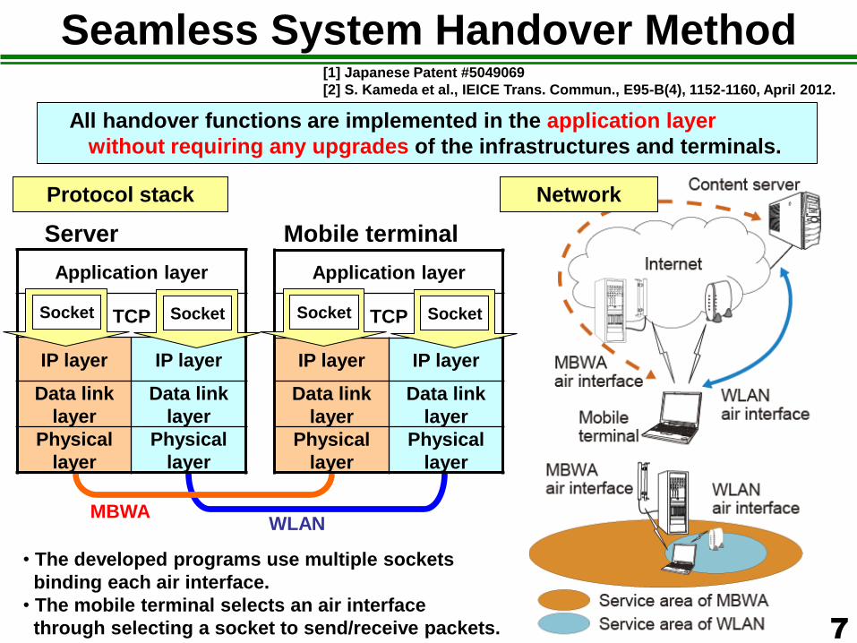
Seamless System Handover Method
Application layer
TCP
IP layer IP layer
Data link
layer
Data link
layer
Physical
layer
Physical
layer
Socket Socket
Application layer
TCP
IP layer IP layer
Data link
layer
Data link
layer
Physical
layer
Physical
layer
Socket Socket
MBWA WLAN
• The developed programs use multiple sockets
binding each air interface.
• The mobile terminal selects an air interface
through selecting a socket to send/receive packets.
Protocol stack
Server Mobile terminal
Network
All handover functions are implemented in the application layer
without requiring any upgrades of the infrastructures and terminals.
[1] Japanese Patent #5049069
[2] S. Kameda et al., IEICE Trans. Commun., E95-B(4), 1152-1160, April 2012.
8
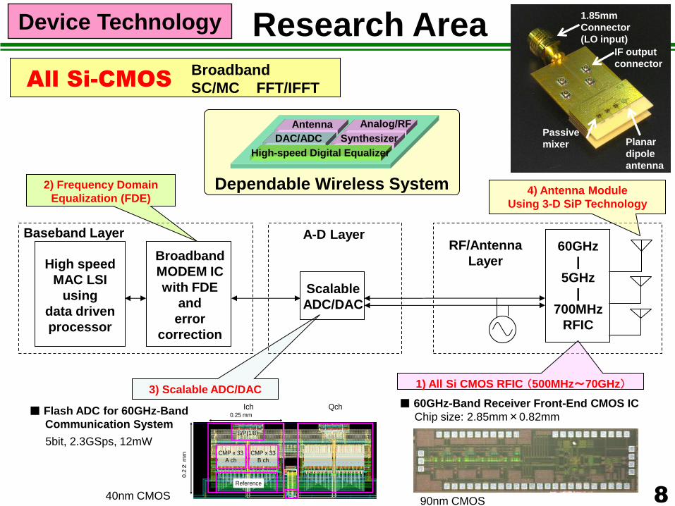
Research Area
60GHz
|
5GHz
|
700MHz
RFIC
Scalable
ADC/DAC
Broadband
MODEM IC
with FDE
and
error
correction
High speed
MAC LSI
using
data driven
processor
A-D Layer Baseband Layer RF/Antenna
Layer
1) All Si CMOS RFIC (500MHz~70GHz)
2) Frequency Domain
Equalization (FDE)
3) Scalable ADC/DAC
■ Flash ADC for 60GHz-Band
Communication System
40nm CMOS
■ 60GHz-Band Receiver Front-End CMOS IC
90nm CMOS
All Si-CMOS Broadband
SC/MC FFT/IFFT
Dependable Wireless System
High-speed Digital Equalizer
DAC/ADC Synthesizer
Analog/RFAntenna
High-speed Digital Equalizer
DAC/ADC Synthesizer
Analog/RFAntenna
Ich Qch
CMP x 33
A ch
CMP x 33
B ch
S/P(1/8)
Reference
0.25 mm
0.22
mm
5bit, 2.3GSps, 12mW
Chip size: 2.85mm×0.82mm
Device Technology
4) Antenna Module
Using 3-D SiP Technology
1.85mm
Connector
(LO input)
IF output
connector
Passive
mixer Planar
dipole
antenna

Heterogeneous Scalable Receiver
for Realizing Dependable Air
Realizing Scalable Frequency Domain Equalization
for Heterogeneous Wireless System
– ASIC Implementation of Baseband Circuit with Scalable FDE
700MHz
Rx
Clock ~ ~ 5GHz
Rx
60GHz
Rx
700M/5G
Conv.
60G/5G
Conv. ~
ASIC Board
SC
MC
IFF
T
A/D
FD
E
Dem
od.
~ ~
~
A/D
FF
T
FPGA
to Tx Channel
Select
2) Frequency Domain
Equalization (FDE)
Channel
Estimation

• Multimode: SC and/or MC signals
• Channel estimation: 2 channels simultaneously
• Two 256-point FFT/IFFT circuits (include 64 point x 4) – Each FFT is also able to work either two 128-point FFTs or four 64-point FFTs.
• Implemented estimation scheme: MMSE and ZF (zero forcing)
Noise
estimator
Weight
calculator RAM
Data equalizer
OUT
(SC)
dr(n)
dr(t)
pr(t)
(Data) Buffer
pr(t) Buffer
Sele
cto
r
FFT
FFT
FFT
FFT
Sele
cto
r Pilot demod.
Sele
cto
r FFT
FFT
FFT
FFT
Sele
cto
r
RAM (Pilot)
IN
IN
IN
Scalable FFT
OUT
(MC)
Multimode FDE Receiver: Design
Block Diagram of Multimode FDE
10

Scalable FFT (64 point x 4)
for compensation
Scalable FFT (64 point x 4)
for channel estimation
Weight Calc.
+ etc.
RAM
RAM
4.7
mm
Multimode FDE Receiver: ASIC implementation
Process 180nm CMOS
Total area
(core area)
22.1 mm2
(17.6 mm2)
Throughput 48.1 Mbit/s at
100 Msample/s
Power
consumption
660mW at
100 Msample/s
FPGA Xilinx Corp.
Virtex4 LX200
Clock frequency 100 MHz
ASIC specifications Evaluation board specifications
FPGA
ASIC socket
CMOS: complementary metal-oxide semiconductor
FPGA: field-programmable gate array 11

12
Surface & Space Communications
Future Direction: Extended Dependable Air
Space
Surface