development of nanosphere lithography … of nanosphere lithography technique with enhanced...
TRANSCRIPT

Development of Nanosphere Lithography Technique with Enhanced Lithographical
Accuracy on Periodic Si Nanostructure for Thin Si Solar Cell Application
by
Jeayoung Choi
A Dissertation Presented in Partial Fulfillment of the Requirements for the Degree
Doctor of Philosophy
Approved March 2015 by the Graduate Supervisory Committee:
Christiana Honsberg, Co-Chair
Terry Alford, Co-Chair Stephen Goodnick
ARIZONA STATE UNIVERSITY
May 2015

i
ABSTRACT
In this thesis, a novel silica nanosphere (SNS) lithography technique has been
developed to offer a fast, cost-effective, and large area applicable nano-lithography
approach. The SNS can be easily deposited with a simple spin-coating process after
introducing a N,N-dimethyl-formamide (DMF) solvent which can produce a highly close
packed SNS monolayer over large silicon (Si) surface area, since DMF offers greatly
improved wetting, capillary and convective forces in addition to slow solvent evaporation
rate. Since the period and dimension of the surface pattern can be conveniently changed
and controlled by introducing a desired size of SNS, and additional SNS size reduction
with dry etching process, using SNS for lithography provides a highly effective nano-
lithography approach for periodically arrayed nano-/micro-scale surface patterns with a
desired dimension and period. Various Si nanostructures (i.e., nanopillar, nanotip,
inverted pyramid, nanohole) are successfully fabricated with the SNS nano-lithography
technique by using different etching technique like anisotropic alkaline solution (i.e.,
KOH) etching, reactive-ion etching (RIE), and metal-assisted chemical etching (MaCE).
In this research, computational optical modeling is also introduced to design the
Si nanostructure, specifically nanopillars (NPs) with a desired period and dimension. The
optical properties of Si NP are calculated with two different optical modeling techniques,
which are the rigorous coupled wave analysis (RCWA) and finite-difference time-domain
(FDTD) methods. By using these two different optical modeling techniques, the optical
properties of Si NPs with different periods and dimensions have been investigated to
design ideal Si NP which can be potentially used for thin c-Si solar cell applications.
From the results of the computational and experimental work, it was observed that low

ii
aspect ratio Si NPs fabricated in a periodic hexagonal array can provide highly enhanced
light absorption for the target spectral range (600 ~ 1100nm), which is attributed to (1)
the effective confinement of resonant scattering within the Si NP and (2) increased high
order diffraction of transmitted light providing an extended absorption length. From the
research, therefore, it is successfully demonstrated that the nano-fabrication process with
SNS lithography can offer enhanced lithographical accuracy to fabricate desired Si
nanostructures which can realize enhanced light absorption for thin Si solar cell.

iii
Dedicated to my beloved parents:
Yi-Sik Choi and Young-Sang Yu

iv
ACKNOWLEDGMENTS
During my Ph.D years, I have received support and encouragement from a great
number of individuals without whom this dissertation might not have been written and to
whom I am greatly indebted.
First of all, I would like to thank Dr. Christiana Honsberg for allowing me to have
such a great opportunity as a Ph.D student in Solar Power Lab – Nano & III-V group.
Because of her valuable advice and kind encouragement, I have greatly enjoyed my Ph.D
years and earned valuable research and life experiences. There is no word to express my
deepest gratitude to my advisor, Dr. Christiana Honsberg.
I would also like to give my sincere appreciation to Dr. Terry Alford, co-advisor,
who has shown his great support and guidance which have been valuable resources for
my research and academic life at ASU.
I would also express my gratitude to Dr. Stehpen Goodnick for accepting to be
my committee member.
Gratitude is extended to Dr. Clarence Tracy who has been willing to share his
valuable knowledge and insight with me. The feedback and assistance that I had from
him have been a great strength to overcome the huddle that I faced during my research.
In addition, I would really appreciate Bill Dauksher (SPL Lab Manager) who has
kindly provided valuable advices and assistance for my experiments in Solar Power Lab.
His help has always made things easier.
I would also like to express my sincere gratitude to Dr. Stuart Bowden who has
advised me in many occasions while I study in Solar Power Lab.

v
Lastly, I would like to give my best thanks to my beloved parents, Yi-Sik Choi
and Young-Sang Yu who always show their unconditional love and support throughout
my life.

vi
TABLE OF CONTENTS
Page
LIST OF TABLE……………………………………………………………………...... x
LIST OF FIGURES…………………………………………………………………...... xi
CHAPTER
1. INTRODUCTION …………………....…….……………………………………….. 1
1.1. Background of Photovoltaic ……………………………….………………….... 1
1.2. Current Status of Photovoltaic……………………………….……………..…… 3
1.3. Nanostructured Si Solar Cells……………………….……………………….…...7
1.3.1. Problem of Conventional Approach and Goal of Nanostructured Si
Solar Cell ….…………………………………………………….………..…7
1.3.2. Current Status: Summary of Nano-lithography Techniques………....……. 9
1.3.3. Current Status: Summary of Nano-fabrication Techniques……….......…... 12
1.4. Aim of This Work………………………………………………………………. 15
2. NANO-LITHOGRAPHY & NANO-FABRICATION ……………………..……… 16
2.1. Deposition of 2-Dimensional Silica Nanosphere (SNS) ………………….…… 16
2.1.1. Motivation and Background………………………………………………. 16
2.1.2. Experimental Section……………………………………………………....18
2.1.3. SNS Dispersibility in Solution…………..…………………………...…… 19
2.1.4. SNS Solution Wettability on Silicon Surface….....……………………..… 21
2.1.5. Capillary Force for Short-range SNS Assembly…………...…..…….…… 24
2.1.6. Convective Force for Long-range SNS Assembly …………………...…... 27

vii
CHAPTER Page
2.1.7. Large-scale Area SNS Monolayer Spin-coating……….……..……….…… 29
2.1.8. Spin-coating of SNS with Various Diameters: Diameter vs. SNS Solution
Concentration …………………………………………………….…......… 34
2.1.9. DMF vs. Other Solvents..…...…………...………………………………… 35
2.1.10. Summary ………………………………………...……………….…….… 36
2.2. Surface Nano-patterning.…....………………………………...……….…….….. 38
2.2.1. SNS Size Reduction by Reactive Ion Etching (RIE) ………………...……. 38
2.2.2. SNS Removal after RIE …………………………….………………….….. 43
2.3. Fabrication of Si NP with Metal-assisted Chemical Etching (MaCE) ……....…. 45
2.3.1. Experimental Section …………………………………………….……..…. 46
2.3.2. SNS Diameter Control with RIE …………………………………..…….... 47
2.3.3. Metal Cathode Layer Deposition for Enhanced Lithographical Accuracy .. 49
2.3.4. Fabrication of Si NP with MaCE Technique……………………………..... 51
2.3.5. Summary.…………………………………………………………….…….. 57
2.4. Fabrication of Si Nano-structures with Different Etching Techniques …..…….. 59
2.4.1. Inverted Pyramid: KOH Solution Etching ………………………….….…...59
2.4.2. Nano-pillar & Nano-tip: RIE.……………………….…………………...… 61
3. OPTICAL SIMULATION FOR SI NANOPILLAR ARRAY ……………..……….. 66
3.1. Background ………………………..…………………………………..….…….. 66
3.1.1. Motivation of This Work….………………………………..…...……….… 66
3.1.2. Rigorous-Coupled Wave-Analysis (RCWA) …………………….……..… 68
3.1.3. Finite-Difference Time-Domain (FDTD) …………………….………..…. 69

viii
CHAPTER Page
3.2. Design of Si NPs for Enhanced Light Absorption …………………………..… 70
3.2.1. Period of Si NPs ……………………………………..……………...……. 70
3.2.2. Height and Si FF of Si NPs ……………………………………...……….. 72
3.2.3. Diffraction Efficiency of Si NPs at Higher Orders (> 0th order) …….….. 77
3.2.4. Absorption Enhancement of Si NP Array ……………………………….…81
3.2.5. Summary …………………………………………………………..………..83
4. FABRICATION OF SI NPS BASED ON OPTICAL MODELING……………….. 84
4.1. Demonstration of Simulated Si NPs ………………………………………....... 84
4.1.1. Fabricated Si NP Vs. Simulated Si NP …………………...…………….… 84
4.1.2. Si NP Vs. Conventional KOH Pyramid …………………………...……... 90
4.1.3. Summary …………………………………………………………………. 91
5. ORGANIC PASSIVATION FOR SI SURFACE ……………………..….………... 92
5.1. Understanding of Molecular Contribution for Effective Quinhydrone/Methanol
Organic Passivation for Silicon……………………………………….………....92
5.1.1. Fundamental of Recombination Process ……………………...…….……..92
5.1.2. Surface Passivation Approaches ………………………….…...……….…..99
5.1.3. Motivation of This Work …………….…………………...………..………99
5.1.4. Experimental Section ………………………………………………….…..101
5.1.5. Minority Carrier Lifetime ………………………………………..………..102
5.1.6. Uniformity of Organic Passivation Layer ……………………….………. 103
5.1.7. Understanding of Molecular Reaction for Passivation …………….....…. 106
5.1.8. Carrier Lifetime Vs. Passivation Time in Solution ……………………….109
ix
CHAPTER Page
5.1.9. Kelvin Probe Measurement: Si Surface Band-Bending ….…………….…110
5.1.10. Summary ………………………………………………………...……... 114
6. CONCLUSION AND PROPOSED FUTURE WORK ……………………..…...….115
6.1. Conclusion ……………………………………………….……………………. 115
6.2. Proposed Future Work ………………………………………………………… 116
REFERENCES …………………………………………………………….…………. 118
APPENDIX
A.1. LIMIT OF ABSORPTION ENHANCEMENT IN THIN-FILM WITH
GRATING STRUCTURE FABRICATED IN SUBWAVELENGTH
-SCALE PERIOD …………………………………………..……………….. 130
A.2. STATISTICAL COUPLED-MODE THEORY …………….……...……….. 130
A.3. OVERVIEW OF THE THEORY ……………………………………………..135
A.4. UPPER LIMIT OF ABSORPTION ENHANCEMENT
IN 2-D GRATING…………………………………………...…………….…..138
A.1-4. EFFECT OF PERIODIC LATTICE STRUCTURE ………...……..…… 139

x
LIST OF TABLES
Table Page
1.1. Performance of Commercial PV Technologies (Data from EPIA, 2011) [11] ......... 5
2.1. Comparison of CHF3 / Ar Gas RIE Etching Profile for 10-min Etching on SS
Deposited Si Surface Which Were Performed under Three Different Chamber
Pressures. ................................................................................................................. 39
5.1. N-type Si - SPV Values (Induced Charge at Si Surface) Measured by Kelvin
Probe, and τeff & Implied Voc Measured by Photoconductivity Decay with
Various Surface Treatments & Passivation (or Dipping) Time. ........................... 111

xi
LIST OF FIGURES
Figure Page 1.1. Historical and Projected World Energy Supply and Demand. [5] ............................... 2
1.2. Average Solar Irradiance Map of the World ...………………………….………..... 3
1.3. Total World Energy Consumption by Sources (2010) ............................................... 4
1.4. Pie Chart of Capacity Percentage of Different Type of PVs. [12] .............................. 6
1.5. The Absorption Length of Crystalline Silicon Juxtaposed Against the Am1.5G
Solar Irradiance. The Blue, Green, and Red Colored Regions Indicate the
Region with the Highest Optical Absorption, the Region with the Highest Solar
Irradiance, and the Region with Absorptions Lengths in Excess of 100μm,
Respectively.[17] ....................................................................................................... 7
1.6. (a) Schematic Illustration of E-beam Generation (Left),[26] and Overall
Patterning Process in 6 Steps (Right),[27] (b) Mechanism of Laser (or Multi-
beam) Interference Lithography Technique (Left), and Possible Patterns with
Different Combination of Lasers (Right). [25] ........................................................ 10
1.7. Schematic Illustration of (a) Nano-imprint Lithography,[29] (B) Nanosphere
Lithography Processes. [28] .................................................................................... 11
1.8. Schematic Illustration of Various Nano-fabrication Method; (a) CVD, (b) RIE,
(c) ECE, and (d) MaCE.[35-38] .............................................................................. 13
1.9. SEM Images of Si Nanowire (or Nanopillar) by Using (a) CVD,[39] (b)
RIE,[40] (c) ECE,[41] and (d) MaCE . .................................................................... 14
2.1. The SNS Cluster Effect Producing Non-uniform SNS Distribution Followed by
Reduced Coverage. .................................................................................................... 21

xii
Figure Page
2.2. Contact Angle Measurement of (a) Water (α = 26.9˚), and (b) DMF (α ≈ 0 or un-
measurable). The Comparison of Wettability with 300ul (50mg/ml) of (c)
SNSwater, and (d) SNSDMF Solution Droplets on Piranha Cleaned 2-inch Si
Substrate, and After-spin-coating Surface Images of (e) SNSwater, and (f)
SNSDMF. ..................................................................................................................... 22
2.3. Schematic Illustration of Material Loss of (a) SNSwater and (b) SNSDMF during
Spinning, and the SEM Images to Compare the Coverages between (c) SNSwater
and (d) SNSDMF. To Focus on Solvent Influence, 50mg/ml of Low SNS
Concentration was Used. Spin-coating Speed is Same for Both. .............................. 23
2.4. Schematic Illustration of Two Spheres Partially Immersed in a Fluid Layer for
Capillary Attraction, Fcap.[61] ................................................................................... 25
2.5. (a) Fcap Plotted as a Function of L, and the Actual SEM Images from (b) SNSwater,
and (c) SNSDMF. (d) and (e) are the Schematic Illustration of Interparticle
Distance, L, Depending of Wettability of Solvent, Water and DMF,
Respectively. (Note: The Fcap Calculation was Made with αwater = 26.9°, αDMF ≈
0 to Determine the Ѱc, rc = 130nm (radius of 2/3 sphere spot), γwater = 73mN/m,
and γDMF = 25mN/m, respectively.) ........................................................................... 26
2.6. Schematic Illustration of (a) Fast Solvent Evaporation of Water, and (b) Slow
Solvent Evaporation of DMF during Spin-coating causing (c) Discontinuous
SNS Assembly with Localized Fcap, and (d) Continuous SNS Assembly after
Expanded Fcap, and Actual SEM Images of (e) SNS water, and (f) SNSDMF
(50mg/ml of SNS with Same Spin-coating Condition). ............................................ 28

xiii
Figure Page
2.7. SEM Images for SNS Coverage from Various Concentration of SNSDMF, which
are (a) 50mg/ml, (b)100mg/ml, and (c) 150mg/ml. ................................................... 29
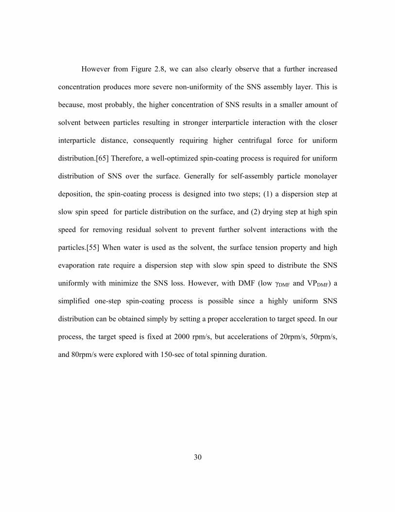
2.8. Acceleration Speed Effect for Uniform SNS Assembly Layer Formation; (a)
20rpm/s, (b) 50rpm/s, and (c) 80rpm/s. ..................................................................... 31
2.9. (a) SNS Deposited 2-inch Round Si Surface Image, and the SEM Images with
Different Magnifications, (b) 250x, c) 2000x, and (d) 25000x, Respectively. ......... 32
2.10. (a) SNS Deposited 4-inch Round Si Surface Image, SEM Images of (b) Low
Magnification, (c) Less SNS Monolayer Coverage Region of Blue Solid-box in
(b), and (d) High SNS Monolayer Coverage Region of Red Solid-box in (b). ....... 33
2.11. Different Size of SNS in (a) 310nm, (b) 600nm, and (c) 840nm Diameters,
Spin-coated on 2-inch Si Wafers (Top, Middle, and Bottom of (a) ~ (c)
Represent the Whole 2-inch Wafer with Each SNS, ×2k, and ×20k
Magnification SEM Images, Respectively.), (d) Optimum SNS Solution
Concentration vs. SNS Diameter for Spin-coating and (e) Table Representing
the Ratio of SNS Diameter (Dia., nm) to Solution Concentration (Conc’,
mg/ml) for Spin-coating. ......................................................................................... 34
2.12. SEM Images of DMSO Introduced SNS (310nm) Spin-coated Si Surface
Which Shows (a) Severely Non-uniform, and (b) Multi-layered SNS Film.
(Note: Spin-coating Condition was 80rpm/sec Acceleration and 2000 rpm/sec
Maximum Speed for 200-sec) ................................................................................. 36

xiv
Figure Page
2.13. (a) Spin-coated 2-inch Round Si Surface Images and SEM Images of (b)
Uniformly Distributed SS and (c) Closely-packed SS Shown in Different SEM
Magnifications. ........................................................................................................ 38
2.14. Schematic Illustration (Top) and SEM Images (Bottom) to Compare the Effect
of RIE Chamber Pressures, (a) As-deposited SS, (b) 75mTorr RIE Processed
SS (Horizontal Dia. ~800nm, Vertical Dia. ~350nm), and (c) 100 mTorr RIE
Processed SS (Horizontal Dia. ~800nm, Vertical Dia. ~260nm). ........................... 40
2.15. (a) ~ (d) SEM Images of RIE Etched SS with Various Etching Times, 10-min,
13-min, 16-min, and 19-min, Respectively, and (e) Diagram of Inter-particle
Spacing (d) Versus RIE Etching Time. (Note: RIE Conditions are 75mTorr
Chamber Pressure, 200 Watts RF Plasma Power at 25/25sccm Gas Flow Rate)
(Scale-bar: 1 um for Top Image, 500nm for Bottom Image). ................................ 42
2.16. Schematic Illustration of SNS Lithography Process and UVO Effect to Produce
Clean Si Surface Patterning, and (e) Bottom is SEM Image of Non-UVO
Treated Sample, and (f) Bottom is UVO Treated Sample. (Green-line Indicates
Deposited Cr Layer, and Red-line Indicates CxFy Compound Layer on the
Surface, Scale-bar = 1 μm) ...................................................................................... 45
2.17. Three Different Sizes of SNS in (a) 310nm, (d) 600nm, and (g) 840nm in
Diameter, and RIE Etched with Two Different Etch Times. (b), (c) are 1.5-min
and 2.5-min on 310nm SNS, (e) and (f) are 4-min and 6-min on 600nm SNS,
and (h) and (i) are 6-min and 8-min on 840nm SNS. (j) the SNS Diameter
Change vs. RIE Time, and (k) a Table Showing Etch Rates for Each SNS. .......... 48

xv
Figure Page
2.18. (a) The Etched Si Nanopillar Had Un-expected Structure Damage by In-
complete SNS Removal due to Metal Catalyst Covered on SNS, and (b) Peel-
off Au Metal Layer during SNS Removal due to Weak Adhesion of Au on
Bare Si Surface. ....................................................................................................... 50
2.19. (a) Si Surface with SNS Etched to 611nm Average Diameter (840nm period),
(b) Cr/Au, (c) Ti/Au, and (d) Ni/Au Deposited Si Surface after SNS Removal
Which Have 722nm, 667nm, and 622nm Diameter of Pattern, Respectively. ....... 51
2.20. Scheme of Reaction Processes for Metal-assisted Chemical Etching Based on
Galvanic Process. ① The Oxidant (i.e., H2O2) is Reduced by the Catalytic
Activity of Noble Metal. ② The Generated Holes from Reduction of Oxidant
Consequently Diffuse to Si/Metal Interface through Metal Layer. ③ The
Oxidation of Si is Occurred by the Injected Holes, and ④ SiO2 is Reacted with
HF. ⑤ Finally, SiO2 is Dissolved and Etched Away into the Solution.[82] .......... 52
2.21. (a), (d), and (g) are RIE Etched SNS with 840, 600, and 310 nm Initial
Diameter. (b), (e), and (h) are Up-side SEM Image, and (c), (f), and (i) are 80
Degree Angled SEM iImages for Si NPs. ............................................................... 54
2.22. Ni/Au Catalyst Deposited Si Surface with (a) 30%, (b) 50%, and (c) 70%
Fractional Coverage, and (d) ~ (f) Si NPs Fabricated from Each Catalyst
Fractional Coverage after 5-min Etching in MaCE Solution. (g) Etch Rates
from Each Ni/Au Fractional Surface Coverage. (h) ~ (j) ~ 500nm Height of Si
NPs from (a) ~ (c) after Dipping in the Etching Solution for 8-min, 6.5-min,
and 5-min, Respectively. ......................................................................................... 56

xvi
Figure Page
2.23. SEM Images of Fabricated Si NP Array at 3 um Height in 840nm Period (50%
Si FF) to Confirm the Uniformity of the Si NP Array Over the Surface; (a)
×35K, and (b) × 10K Magnifications. ..................................................................... 57
2.24. SEM Images of (a) Cr Deposited Si Surface after SNS Removal, (b) 1% KOH
Etched Surface with Cr Layer, (c) Inverted Si Pyramid after Cr Layer
Removal, (d) Cross-sectional Image of Inverted Si Pyramid, and (e) Fabricated
Inverted Pyramid over Large Surface Area to Show Its Uniformity (Inverted
Pyramid Has ~10% Size Variation Likely Caused by an Initial SNS Size
Variation of 10%). Note : (a) ~ (d) Scale-bar = 1 μm, and (e) Scale-bar = 10
μm. ........................................................................................................................... 60
2.25. Schematic Illustration of RIE Process to Etch Solid Surface.[83] ........................... 63
2.26. Schematic Illustration and SEM Images to Fabricate Nanopillar and Various
Aspect-ratio Nano-tip Structure. ............................................................................. 64
3.1. (a) Shematic Illustration of Simulated Si NP, and (b) Investigated Optical
Properties of Si NPs Arrayed in 2-D Hexagonal Formation; (1) Forward
Scattering for Reduced Front Surface Reflection Loss, and (2) Light Diffraction
Order for Enhanced Light Absorption of Transmitted Light in the Absorber. ......... 68
3.2. Constructed Structure to Solve a Diffraction Problem Using RCWA. (a)
Structure Is Divided into Strata so That Each Stratum Is Homogeneous in the Z-
direction, and (b) Horizontally Divided Strata so That Each Stratum Is
Homogeneous in the y-direction for Circular-shaped Structure Calculation. ........... 68
xvii
Figure Page
3.3. Upper Limit of Absorption Enhancement for a Grating with Hexagonal Lattice
Periodic Structure. Reprinted from Reference [98] ................................................... 71
3.4. Schematic Illustration of Grating Structured Layer for (a) Statistical Coupled-
mode Theory, and for (b) Our Simulation. ................................................................ 73
3.5. RCWA Results for Front Surface Reflections from Three Different Si FFs, (a)
30%, (b) 50%, and (c) 70% Representing 344, 444, and 520 nm Si NP
Diameters, Respectively, and the Height Range Is from 100 to 400nm with
100nm Interval. In Addition, (d) Reflection Trends for Short (300~600nm) and
Long (600 ~ 1100nm) λ Are Shown with Different NP Heights in Weighted
Reflectance. (Note: Period Is Fixed at 600nm) ......................................................... 74
3.6. Incident Light Scattering Behavior (λ = 900nm) with Various Heights; (a)
100nm, (b) 200nm, (c) 300nm, and (d) 400nm at 30% Fixed Si FF ......................... 75
3.7. Incident Light Scattering Behavior (λ = 900nm) with Various Si FF; (a) 30%, (b)
50%, (c) 70% at 200nm Fixed Height ....................................................................... 76
3.8. Red-shifting of Front Surface Reflection as (a) FF (or Diameter, at 100nm
Height) and (b) Height (at 70% FF) Increases. ......................................................... 77
3.9. Schematic Illustration of Light Loss Mechanisms for Incident Light in Short
(Blue Arrow), and Long (Red Arrow) Wavelength Region ...................................... 78
3.10. Optical Simulation for Transmitted Light Orientation with (a) FDTD (λ =
1000nm), and (b) RCWA ........................................................................................ 79
3.11. Schematic Illustration of Grating Effect with Si NP to Produce High Order
Transmitted Light Diffraction ................................................................................. 79

xviii
Figure Page
3.12. Fraction of High Order (>0th) Transmitted Light Diffraction with (a) 30%, (b)
50%, and (c) 70% Si FF at Various Height from 100nm to 400nm ........................ 81
3.13. RCWA Results for Feflection of Si NP Fabricated at 30% FF, 200nm Height
and 600nm Period and Reference Reflection from Bare Si surface (5 µm Thick
Si Substrate). Both Surfaces Have Back Reflector (BR, 200nm in Perfect
Mirror Condition) and Front Anti-reflection Layer (AR, 70nm SiNx). .................. 82
4.1. Fabricated 30% FF Si NPs in 600nm Periodic Hexagonal Array Approximately
for (a) 100nm, (b) 200nm, (c) 300nm, and (d) 400nm Heights ................................. 85
4.2. Measured Reflectance of Si NPs at Different Heights ............................................... 86
4.3. Comparison of Surface Reflection between Computational (RCWA, Dash-line)
and Measured (Measured, Solid-line) Reflection for (a) 100nm, (b) 200nm, (c)
300nm, and (d) 400nm Si NP Heights (Measured Si Substrate Thickness = 280
µm and RCWA Simulated Si Substrate Thickness = Semi-infinite) ......................... 87
4.4. Comparison of Measured (Red Solid-triangle) and RCWA Simulated (Blue
Solid-diamond) Weighted Reflection Change for (a) Whole Wavelength Range
(300 ~ 1100nm), (b) Short (300 ~ 700nm) and (c) Long (700 ~ 1100nm) λ
Region with Increasing Si NP Height ....................................................................... 88
4.5. Example of Structural Damage on Top of 400nm Si NP in Red-circle ..................... 89
4.6. Comparison of Surface Reflection between Si NPs (Red Solid-line, 200nm
Height, 30% FF, and 600nm Period) and Conventional KOH Solution Etched
Random Pyramid (Black Solid-line) Fabricated on 280 um Si Substrate. ................ 90
5.1. Carrier Recombination Mechanism in Semiconductor System.[103] ....................... 94

xix
Figure Page
5.2. Molecular Structures of (a) BQ, (b)HQ, (c) QHY, (d) SQ (Passivation Agent). ..... 100
5.3. (a) Measured Minority Carrier Lifetimes (τeff) of BQ (Solid-square) and HQ
(Solid-triangle) Treated Si Compared to an HF (Open-circle) Only Cleaned
Sample and (b) the Measured τeff at a Minority Carrier Density of 2x1015 cm-3
with 100% BQ, HQ, and Various HQ Mixture ratios into a Fixed 10mM BQ in
MeOH. ..................................................................................................................... 103
5.4. HR-AFM Images of (a) Pure BQ, (b) 5 mM HQ, (c) 10 mM HQ, (c) 15 mM HQ
Addition into 10 mM of BQ in MeOH. (Scan-scale : 200 nm x 200 nm & Scale-
bar : 50nm) .............................................................................................................. 104
5.5. TUNA Image of (a) 5 mM HQ, (e) 10 mM HQ, (f) 15 mM HQ Addition into 10
mM of BQ in MeOH. (Scan-scale : 200 nm x 200 nm & Scale-bar : 50nm),
(Note: It Is Note-worthy that a 1 to 1 Mixture Ratio of BQ and HQ Might also
Produce a More Ordered Molecular Stacking of the Passivation Layer since the
Higher Current Flow (or Brighter Color) at the Molecular Island Region in
Figure.5 (b) Might Indicate That There Is a Well-ordered Pi-Pi Stacking
Formation among Molecules Which Improves the conductivity of the Molecular
Layer.[114, 127, 128]) ............................................................................................. 105
5.6. Schematic Illustration for SQ Formation in Solution to Produce Si-SQ Bonding
for Si Surface Passivation ........................................................................................ 107
5.7. (a) FT-IR Results of BQ, HQ, and Various HQ Mixture Ratios into Fixed BQ in
MeOH and Pure MeOH, (b) Reducing BQ into One SQ in BQ/MeOH, (c) Two
SQ Formation in BHQ/MeOH. ................................................................................ 108

xx
Figure Page
5.8. Measured τeff of Si Samples after Dipping in Pure BQ and HQ Added MeOH
Solution for 10-min to 180-min. .............................................................................. 109
5.9. HR-AFM Images of Si Surface after Dipping in BHQ [a, b] and BQ Solution [c,
d] for 1-hr and 3-hr, Respectively. (scale-bar = 50nm) ........................................... 112
5.10. Schematic Illustration of (a) SQ in Mono-layer, and (b) SQ in Aggregation (or
Multi-layer) Producing Different Degree of Molecular Dipole Moment .............. 113
A1. Light Trapping with Random Texture and a Grating Structure. (A) Light
Trapping by Randomly Textured Surface. (B) Light Trapping Using a Periodic
Grating on a Back-Reflector (Yellow); d = 2 μm, L = 250 nm. The Depth and
Width of the Dielectric Groove in the Grating are 50 and 175 nm, Respectively.
The Dielectric Material is Crystalline Silicon. (C) Absorption Spectrum
[Transverse Magnetic (TM) Mode, Normal Incidence] and Dispersion Relation
of Waveguide Modes for the Structure in B. Resonances Occur When k// =
2π/L (Red Dots). Reprinted from Reference [103]. ................................................. 131
A2. (a) Channels in 2-D k-space for a Grating with the Square Lattice Periodic
Structure and (b) its Upper Limit of Absorption Enhancement. Reprinted from
Reference [102] ....................................................................................................... 137
A3. (a) Channels in 2-D k-space for a Grating with Hexagonal Lattice Periodic
Structure and (b) its Upper Limit of Absorption Enhancement. Reprinted from
Reference [102] ....................................................................................................... 139

1
Chapter. 1
INTRODUCTION
1.1. Background of Photovoltaic
After the discovery of the photovoltaic effect by Becquerel in 1839,[1] numerous
scientific and technical successes have been achieved to develop the first silicon solar
cells based on a diffused p-n junction at Bell labs in 1954.[2] Since the first foot step of
Si solar cell, solar cell industry has been rapidly grown and in 2014, ~ 45 giga watt (GW)
capacity of solar panels have been installed around the world.[3] This phenomenal
growth of solar industry has been motivated by global warming originated from the
excess carbon dioxide emission from traditional fossil fuel based power generation. In
addition, the risk of nuclear power which can produce almost irretrievable damage both
to human-being and environment make itself less ideal energy resource regardless of its
meager chance of accident. Therefore, there is growing interest in developing clean and
renewable energy to sustain human life accompanied by preserving our nature.
In addition to drawbacks of traditional power generation methods, recent global
population growth and rapid industrialization in 3rd world undeveloped countries have
casted a huge question how we will satisfy the exponential demand of energy in the
future to sustain our society. The question must be considered very seriously since as
shown in Figure 1, the global demand of energy will be exceeded far beyond possible
energy supply from traditional fossil fuel based energy generation.[4, 5] This energy
shortage has significant implication to the future of our society. For example, in order for

2
10 billion people to sustain their current level of lifestyle, the world needs at least ten
additional terawatts (TWs) which is equivalent to 150 millions of barrels of oil per day
until 2050.[6, 7] Furthermore, the energy crisis will be more exacerbated by the concerns
about global warming from greenhouse gas emission due to increasing fossil fuel
consumption. [8-10] Therefore, developing clean, un-depletable, and less geometrically
dependent energy resource is the major and very first challenge of our society to continue
the prosperity of human-being in this world.
Figure 1.1. Historical and projected world energy supply and demand. [5]

3
1.2. Current Status of Photovoltaic
In terms of the effort to find new energy resource, recently various kind of clean
and renewable energy resources and generation techniques have been developed
including biomass, geothermal, wind, and solar energy. However, among these resources,
solar energy is considered as the most ideal candidate for future energy resource which
can satisfy the conditions as clean, un-depletable, and less geometrically dependent
energy source. In Figure 2 for average solar irradiance map of the world clearly shows
that the enormity of the distributed solar resource and its highly open accessibility
regardless of location. Therefore, solar energy has a huge potential to replace
conventional fossil fuel in addition to its safety.
Figure 1.2. Average solar irradiance map of the world. (Copyright Mines Paristech/Armines 2006)

4
Figure 1.3. Total world energy consumption by sources (2010)
As shown in Figure 3, however, fraction of world energy consumption from solar
energy is less than 0.1% among total world energy consumption. In addition, even
compared with other renewable energy resources, energy supply from solar is still too
meager to be meaningful energy supply source. The major barrier for this very limited
energy consumption from solar energy is attributed to the high cost and/or insufficient
efficiencies of existing solar cells. Therefore, many of recent PV researches have focused
on developing high or reasonable efficiency of solar cells accompanied by economical
viability to compete with traditional fossil fuel.

5
Table 1.1. Performance of commercial PV technologies (Data from EPIA, 2011) [11]
In Table 1, commercially available solar cells are listed with their performances,
[11] and from the Table 1, it is obvious that conventional bulk (or thick) c-Si PV still
offers superior performance compared to newly developed PV with different materials
which has developed to provide cost-effective PV. This inferior performance of newly
developed PV cannot provide sufficient grid parity (i.e. the parity between the PV
generation cost for residential and commercial systems and the electricity retail price for
householders) due to their poor performance despite the lower mass production cost
compared to convention bulk c-Si PV. Furthermore, suitable PV processing technologies
must be developed to produce PV from new material with reasonable grid parity.
However, unlike c-Si PV which already made tremendous advancement in the

6
microelectronics, metal contact, and dielectric passivation techniques due to the long
history of c-Si PV and its technical compatibility with Si based semiconductor area, the
immature technical and infrastructural basement of new PVs is considered as a barrier for
their continuous development. Therefore, as shown in Figure 4, conventional bulk c-Si
PV is still playing a dominant role in the global PV market.[12]
Figure 1.4. Pie chart of capacity percentage of different type of PVs.[12]
However, as discussed previously, despite the numerous advantages of bulk c-Si
PV, the high production cost has prevented its wide deployment to replace traditional
energy resources. Therefore, milestone innovation must be achieved to improve its
efficiency and/or economical viability.[13, 14]

7
1.3. Nanostructured Thin Si Solar Cells
1.3.1. Problem of conventional approach and goal of nanostructured Si solar cells
To produce a cost-effective, but high efficiency Si PV, there is a growing
attention for thin c-Si PV to save material cost which has 20~30% of total module cost.[]
In addition, thin Si PV also has a great potential for increased efficiency compared to
bulk Si PV since thinner absorber produces less bulk recombination for increased short-
circuit current (JSC) and recent state-of-the-art amorphous Si (a-Si) passivation technique
has achieved more than 750mV open circuit voltage (VOC) with thinner Si wafer.[15, 16]
Figure 1.5. The absorption length of crystalline silicon juxtaposed against the AM1.5G solar irradiance. The blue, green, and red colored regions indicate the region with the highest optical absorption, the region with the highest solar irradiance, and the region with absorptions lengths in excess of 100μm, respectively.[17]

8
Reduction in absorber thickness for commercial Si solar cells requires multiple
elements to come together, including thin wafers; good surface passivation; low
temperature processing; and a high degree of light absorption. Among these elements,
particularly, demonstration of high degree of light absorption with thin Si wafer has been
one of major concerns in the field due to the material limit of Si conveying low
absorption coefficient at longer wavelength region which requires significantly increased
light absorption length as shown in Figure 5. However, the thin Si wafer only provides a
short optical length; in a consequence, large fraction of light loss, especially from longer
wavelength region, will be expected. Therefore, special surface architecture must be
introduced to increase optical length of physically thin Si absorber.
In general, surface texturing is the most widely used approach to increase light
absorption of Si solar cells which can provide significantly reduced surface light
reflection. The most well-known method for c-Si texturing is anisotropic etching in
alkaline solution such as KOH to texture the surface with randomly arrayed pyramids
having dimensions in the range of several microns.[18] However, this conventional
pyramid structure is not ideal for thin Si solar cell application due to its large material
loss during etching process in addition to its insufficient optical property.
Nano-scaled Si surface texturing, therefore, has been widely studied to replace
conventional large-scaled pyramid structure due to its reduced material loss from etching
process in addition to its highly enhanced AR effect and light absorption.[19, 20]
However, regardless of the great potential of Si nanostructures, their excess close-
packing and high aspect-ratio have been considered as main barriers to produce high
efficiency nanostructured Si solar cell. This is because its complicated surface geometry

9
is highly challenging for effective surface passivation [21-23] and intimate electrode
contact [6] which produce large surface defect density and poor photo-generated carrier
extraction, respectively. In a consequence, poor performance of fabricated device is
unavoidable. Therefore, well-designed Si nanostructure must be presented which can
offer not only enhanced optical path length within thin Si absorber, but also high level of
process compatibility for high performance device fabrication.
1.3.2. Current Status: Summary of Nano-lithography techniques
Prior to fabrication of nanostructure on Si surface, highly well-defined surface
patterning in nano-scale must be introduced to determine the period, dimension and/or
shape of nanostructures since the structural optical properties can be varied depending on
physical conditions of fabricated nanostructure. For surface patterning, optical
lithographic techniques are the major conventional lithographic approach which create
pattern through the use of photons or electrons to modify the chemical and physical
properties of the resist. However, nano-fabrication with photo-resist based lithography
has limited resolution due to diffractive effects.[24] Since a large number of research
groups are working on nanostructure to utilize diverse electrical, physical, and optical
advantages of nano-scaled structure, electron beam lithography (Figure 6 (a)) and laser
interference technique (Figure 6(b)) have been widely developed to fabricate
nanostructures in a desired physical dimension due to their high lithographical resolution
for 1-D or 2-D structure in periodic or aperidic array.[25] These techniques, however, are

10
not adequate for wide application due to their time-consuming, expensive, and small area
restricted processes.
Figure 1.6. (a) Schematic illustration of e-beam generation (left),[26] and overall patterning process in 6 steps (right),[27] (b) mechanism of laser (or multi-beam) interference lithography technique (left), and possible patterns with different combination of lasers (right).[25]
Because of these barriers from conventional nano-lithography processes, a lot of
researches are ongoing to find a cost-effective, less time-consuming and large area nano-
lithography process that provides acceptable lithographical accuracy and reproducibility.
As a part of this effort, currently various novel nano-lithography and fabrication
techniques have been developed and investigated for their wide application. Nano-
imprint lithography technique, Figure 7(A), is one of those and it has been proven its

11
great potential as a highly accurate nano-lithography approach which also offers
enhanced capability for large-area application.[28-30] However, regardless of the great
potential of nano-imprint lithography technique, it still requires conventional nano-
lithography processes including electron beam,[31] and laser interference lithography[32]
techniques to fabricate a master mold to produce secondary mold for nano-imprinting
process. Nanosphere lithography (NSL), Figure 7(B), approach, therefore, has been
widely studies since NSL can produce directly nano-patterned surface using nanosphere
as a mask layer for etching, but also the patterned surface can be used as a master mold
for nano-imprinting application.[33] Furthermore, NSL provides convenient control of
the lithographical scale just by introducing different sizes of nanospheres to fabricate
intended scales and shapes of nanostructure on the surface by using proper etching
techniques.
Figure 1.7. Schematic illustration of (A) nano-imprint lithography,[28] (B) nanosphere lithography processes. [34]
12
In our research, therefore, we have introduced and developed nanosphere
lithogpraphy (NSL) technique rather than nano-imprint process because of its wider
applications.
1.3.3. Current status: Summary of Nano-fabrication techniques
In addition to nano-lithography methods, nano-fabrication process is also highly
crucial to produce nanostructure in an intended physical dimension without any change
for fabricated nanostructure. Fortunately, due to the key role of Si material in modern
semiconductor area and the immense potential of Si nanostructure for various
applications, enormous developments in nanotechnology have been made in the past
decades and wide range of Si nanostructures from 0-D to 3-D have been demonstrated,
such as nanocrystals,[35] nanowire (or nanopillar),[36] nanotube,[37] and porous Si.[38,
39]

13
Figure 1.8. Schematic illustration of various nano-fabrication method; (a) CVD, (b) RIE, (c) ECE, and (d) MaCE.[40-43]
Modern nano-fabrication methods can be roughly divided into two categories
which are (1) bottom-up and (2) top-down structure fabrication methods. The bottom-up
method basically introduces seed materials (or growth catalyst) on the Si surface to
facilitate the growth of nanostructure. In case of top-down method, it is relatively
straight-forward compared to bottom-up method since nanostructures can be prepared
through dimensional reduction of bulk Si by introducing proper etching techniques which
determine the shape of fabricated nanostructure. In Figure 8, examples of currently
available nano-fabrication methods are presented with their rough etching mechanism

14
including chemical vapor deposition (CVD),[43] reactive-ion etching (RIE),[42]
electrochemical etching (ECE),[41] and metal-assisted chemical etching (MaCE).[40]
Figure 1.9. SEM images of Si nanowire (or nanopillar) by using (a) CVD,[44] (b) RIE,[45] (c) ECE,[46] and (d) MaCE.
In Figure 9, four different Si nanowire (or nanopillar) are shown which fabricated
by different nano-fabrication techniques mentioned previously. Each SEM images well
represent the overall nano-fabrication nature of each technique. Specifically, in our
research, we have chosen MaCE process to fabricate Si nanopillar (Si NP) and this is
because (1) CVD process is highly challenging to control the dimension and orientation
of structure in addition to its high-cost, (2) RIE process produces certain amount of
15
under-cutting of structure during etching which causes unexpected physical dimension
change, and (3) ECE process is highly challenging to control the etching rate for desired
nanostructure fabrication. On the other hand, MaCE can offer a fast and low-cost etching
process that also achieves effective vertical etching with minimal size variation of the
NPs from top to bottom.
1.4. Aim of This Work
The aim of this dissertation is to develop fast, cost-effective nano-fabrication
process which can produce highly accurate Si nanostructure in a desired period and
physical dimension. Via our nano-fabrication approach, we have fabricated various
nanostructures including Si nanopillar, nanotip, nanohole and inverted pyramid.
Especially, we have investigated the optical property change of Si nanopillar depending
on the structural dimension. In particular, (1) grating effect of periodic Si NP array will
be computationally studied by using rigorous coupled wave analysis technique and (2)
scattering behavior of Si NP will be also investigated with finite-difference time-domain
(FDTD) method. From the computational work, we will fabricate the Si NP to compare
the results from experimental and computational works to find ideal Si NP dimension
which can provide not only enhanced optical property for thin Si solar cell application,
but also potentially high compatibility with actual device fabrication process.

16
Chapter. 2
NANO-LITHOGRAPHY & NANO-FABRICATION
2.1. Deposition of 2-Dimensional Silica Nanosphere (SNS)
2.1.1. Motivation and Background
High uniformity and large area substrate coverage are fundamental requirements
for self-assembled colloidal particle monolayer deposition processes to be used in
nanosphere lithography.[47-49] A variety of techniques have been explored to produce
uniform colloidal particle monolayer assembly, including Langmuir-Blodgett
deposition,[50, 51] convective self-assembly,[52, 53] and dip-coating.[54] Even though
these techniques have successfully provided close-packed colloidal particle monolayers
with high uniformity, substrate area limitations and slow processing are barriers for their
wider scale use.
Because of these issues, spin-coating methods have been developed to offer fast
and inexpensive large-area colloidal particle monolayer assembly.[55] However, the poor
silicon surface wettability or fast evaporation rate during spin-coating of the commonly
chosen solvents (e.g. water) have made the spin-coating process challenging.[49, 55]
Therefore, there is a clear need for well-designed material preparation and an improved
spin-coating process that leads to a well close-packed colloidal particle monolayer
assembly with high coverage.

17
Previous reports have addressed these conventional solvent issues in several ways.
In one approach, additional surfactant mixtures were added to induce improved solution
wettability and colloidal particle dispersion in solution in addition to delayed evaporation
rate.[56, 57] However, many surfactant approaches are restricted to low density
polystyrene spheres (PS ~1.0 g/cm3) where it is relatively easy to produce a direct effect
by adding small amount of surfactant.[49, 57] For example, Triton-X is a widely used
surfactant for improved interparticle interaction and delayed evaporation rate of methanol
based PS solutions and is typically mixed in a 1 : 400 ratio for enhanced quality PS spin-
coated films.[57, 58] This surfactant approach is very challenging for the high density
silica spheres dispersed in water which has a high surface tension at the liquid/solid
interface as shown in Figure 3(a). A relatively large amount of the highly viscous Triton-
X is required which makes it more difficult to produce a uniform monolayer of silica
spheres even with a delayed solvent evaporation rate. Other than Triton-X, ethylene
glycol (EG) is reported as a surfactant and the spin coating of colloidal silica films on 1-
inch square glass substrates was demonstrated.[56] However, the high viscosity of EG
(16.9 cP at 25°C, water = 1.0 cP) causes the same issues as Triton-X. Therefore, it is
challenging to find the right surfactant and its optimal mixture ratio for silica sphere spin-
coating. Takashi et.al. have introduced a no-surfactant spin-coating method; however,
this method requires additional control of the humidity and temperature during spin-
coating in order to slow the solvent evaporation rate and resulted in only 72% average
SNS coverage on a 2-inch round surface area.[55] Additionally Jiang et.al., reported a no-
surfactant spin-coating method to create non-close-packed SNS arrays but it requires a
surface polymerization process for improved wetting.[59]

18
We introduce the use of the organic solvent, N,N-dimethyl-formamide (DMF) for
silica nanosphere (SNS) monolayer spin-coating on Si surfaces which shows great
potential for high-throughput spin-coating processing. We show that the DMF can
replace the conventional solvents, and provide enhanced uniformity and coverage of a
close-packed SNS monolayer on large surface areas (> 2-inch round Si surface) even
under ambient laboratory spin-coating conditions. The quality of SNS assembled
monolayers and the coverage after spin-coating with the DMF solvent are compared to
films made with the most widely using solvent, water.
2.1.2. Experimental Section
Both the experimental DMF and control water solvent solutions were prepared in
the laboratory and spin coated on identical substrates. The SNS solution was prepared
with a powder of 310nm diameter silica nanospheres (Bang Lab.) which were dissolved
either in the solvent, DMF (Sigma-Aldrich) or de-ionized water (DI-water). The solutions
were sonicated for 5 hours to produce complete dispersion of SNS in the solution. 2-inch
and 4-inch round polished n-type Si (100) substrates (280μm and 460μm thickness,
respectively) were cleaned in a piranha solution [H2SO4 (96%):H2O2 (30%) = 4:1] for
15-min to form a hydrophilic Si surface followed by 10-min DI-water rinse.
SNS solution and its monolayer were evaluated with various characterization
techniques. The SNS dispersion for each solvent was characterized by measuring
absorbance using a UV-VIS spectrophotometer. The SNS spin-coated samples were

19
observed by scanning electron microscopy (SEM, JEOL XL-30), and the coverage of the
SNS monolayer was calculated by the direct counting of the SNS covered area on the Si
surface through image analysis software, “image J” (National Institutes of Health,
USA)18, which has been widely used for particle related surface analysis.13, 19-23 The
wettability of solvent on a Si wafer was determined by measuring the contact angle with
an EasyDrop contact angle measurement system (KRUSS).
2.1.3. SNS Dispersibility in Solution.
Prior to SNS spin-coating, the SNS must be well-dispersed in the solution to
avoid aggregated SNS deposition on the surface. In Figure 2.1(a), we show the
normalized absorbance of 0.5wt% 310nm SNS in DMF and water and compare to the
calculated absorbance based on the extinction cross-sections of isolated SNS in each
solvent. Mie theory was used to fit the experimental results and to compare SNS
dispersibility.[60] The data shows that DMF produces a high level of SNS dispersibility
in the solution since the experimental absorbance behavior of SNSDMF (DMFUV-VIS, red
solid-line) has a well-matched trend with its calculated absorbance (DMFCalc. red dash-
line), indicating SNSDMF was in nearly complete dispersion. For SNS in water (SNSwater),
however, the experimental absorbance (WATERUV-VIS, black solid-line) is substantially
broadened compared to the calculated absorbance (WATERCalc., black dashed-line),
which suggests that larger than 310nm SNS exist in the water and therefore supports the
fact of clustering of SNSwater.

20
Figure.2. 1. SNS dispersibility comparison between DMF and water; (a) absorbance (a.u.) plotted by UV-VIS spectrophotometer measurement (UV-VIS), and calculation (Calc.) of a single 310nm SNS in each solvent. SEM images of (b), and (c) shows SEM images of the SNS assembled surfaces with SNSDMF, and SNSwater, respectively.
Figure 2.1 (b) and (c) are SEM images of the spin coated films on silicon with the
water and DMF solvent solutions, respectively. Consistent with the absorbance data,
there are no noticeable SNS clusters observed on SNSDMF based films shown in Figure
2.1(c), in contrast to that of SNSwater, Figure 2.1(b). The existence of SNS clusters in the
solution is especially problematic during spin-coating since they produce anchored SNS
clusters in the middle of the surface consequently acting as a barrier for subsequent SNS
to be distributed beyond that cluster. As shown in Figure 2.2, the non-dispersed SNS
cluster in the solution produces a large SNS-free area that follows the radial direction of
the substrate and significantly affects the coverage of SNS after spin-coating. Therefore,
a high level of SNS dispersibility in solution must be achieved in advance to produce
good uniformity and coverage of an SNS assembled monolayer with spin-coating.

21
Figure 2.1. The SNS cluster effect producing non-uniform SNS distribution followed by reduced coverage.
2.1.4. SNS Solution Wettability on Silicon Surface.
The contact angles (α) of DMF and water on the Si surface which has a thin
hydrophilic wet-oxide formed by piranha cleaning were measured to compare the degree
of wettability of each solvent. From Figure 2.3 (a) and (b), it is clear that DMF offers an
outstanding wettability (αDMF ≈ 0, un-measurable) when compared to water (αwater = 26.9˚)
on the piranha-cleaned Si surface. The importance of solvent wettability has been
mentioned in early reports, and those show that wetting of solvent is a crucial factor to
obtain uniform colloidal particle monolayer coverage.[49] This is because the high
wettability of solvent can provide fast, uniform, and omnidirectional solution spread-out
during spinning (or even before spinning) due to its low surface tension (γ) at the
liquid/solid interface. For a direct wettability comparison, 300μl of 100mg/ml SNSwater
and SNSDMF solutions were dispensed on piranha cleaned 2-inch round Si wafers. From

22
Figure 2.3 (c), and (d), the SNSDMF solution revealed a complete wetting layer; in
contrast, the same volume of SNSwater solution produced only a partially covered surface
due to its poor wettability.
Figure 2.2. Contact angle measurement of (a) water (α = 26.9˚), and (b) DMF (α ≈ 0 or un-measurable). The comparison of wettability with 300ul (50mg/ml) of (c) SNSwater, and (d) SNSDMF solution droplets on piranha cleaned 2-inch Si substrate, and after-spin-coating surface images of (e) SNSwater, and (f) SNSDMF.
In Figure 2.3 (e) and (f), we compare wafer images after spin-coating of the
SNSDMF and SNSwater solutions to observe the influence of wettability on quality of
assembled SNS layers. These images demonstrate that DMF can produce a highly

23
uniform SNS assembled layer from center to edge, while using water as a solvent gives
rise to a non-uniform layer. This significantly improved uniformity can be explained by
the low γ of DMF (γDMF = 25mN/m) compared to that of water (γwater = 73mN/m). A high
γ solvent (e.g., water) requires higher centrifugal force (or high spin speed) for solution
distribution, but as the spin speed increases, there is a faster solvent evaporation rate
which prevents the SNS from uniform distribution (lack of lubricant) and assembly (lack
of media between the SNS).
Figure 2.3. Schematic illustration of material loss of (a) SNSwater and (b) SNSDMF during spinning, and the SEM images to compare the coverages between (c) SNSwater and (d) SNSDMF. To focus on solvent influence, 50mg/ml of low SNS concentration was used. Spin-coating speed is same for both.
In addition to impacting uniformity, γ is also crucial to determine SNS coverage
on the surface. This is because the lower γ solvent enables a slower spin speed for SNS

24
distribution which reduces the SNS loss at the substrate perimeter. High γ and therefore
high spin speed inevitably produces a large loss of SNS due to the strong centrifugal
force as schematically illustrated in Figure 2.4 (a). The resulting effect is shown in the
SEM images in Figure 2.4 (c) and (d), where SNSDMF, Figure 2.4 (c), reveals noticeable
coverage improvement when compared to SNSwater as shown in Figure 2.4 (d). (Note: the
SEM images were taken from exact center of each sample to exclude possible secondary
SNS delivery during solution spreading.) Therefore, the excellent wettability (or low γ) of
DMF offers both improved uniformity of the SNS assembled layer and enhanced
coverage. (Note: 50mg/ml of low SNS concentration was used to focus on solvent
influence.)
2.1.5. Capillary Force for Short-Range SNS Assembly
To produce a highly close-packed SNS assembled monolayer with spin-coating,
the capillary force (Fcap) between the nanospheres must be considered. This is because
Fcap is mainly the force occurring between each single SNS; therefore, the SNS packing
in a short range assembly (or capillary assembly) is directly affected by the degree of Fcap
which can be calculated by Eq. (1) below;
2 Ѱ 1/ (1)

25
where, as illustrated in Figure 2.5, γ is the surface tension of the liquid, rc is the radius of
the three-phase contact line at the particle surface, Ѱc is the mean meniscus slope angle at
the contact line, and L is the interparticle distance (the distance between the centers of the
particles).
Figure 2.4. Schematic illustration of two spheres partially immersed in a fluid layer for capillary attraction, Fcap.[61]
Based on Eq. (1), we have calculated and plotted the Fcap of the SNS in DMF and
water, respectively, and the results are shown in Figure 2.6. From the diagram in Figure
2.6 (a), the Fcap of DMF never exceeds that of water at the same interparticle distance, L,
since γDMF (25mN/m) is significantly lower than γwater (73mN/m). However, the SEM
images of Figure 2.6 (b) and (c) show that after spin coating both solutions provide a
highly close-packed SNS assembled layer. A reason for this effect may be because the
enhanced wetting of the SNSDMF solution results in a higher density of SNS located near
the surface than that of SNSwater, reducing L as schematically illustrated in Figure 2.6 (d)
and (e). We counted the SNS covered areas from SNSDMF and SNSwater for the same
surface area and the results showed that despite the significantly low γDMF compared to
γwater, SNSDMF provides ~97% of SNS packing to that of SNSwater which proves that DMF
provides a comparable Fcap to that of water to produce a highly close-packed SNS
assembled monolayer after spin-coating.

26
Figure 2.5. (a) Fcap plotted as a function of L, and the actual SEM images from (b) SNSwater, and (c) SNSDMF. (d) and (e) are the schematic illustration of interparticle distance, L, depending of wettability of solvent, water and DMF, respectively. (Note: The Fcap calculation was made with αwater = 26.9°, αDMF ≈ 0 to determine the Ѱc, rc = 130nm (radius of 2/3 sphere spot), γwater = 73mN/m, and γDMF = 25mN/m, respectively.)
2.1.6. Convective Force for Long-Range SNS Assembly
For highly uniform and close-packed SNS assembled monolayer deposition with
spin-coating, two main processes must be considered. The first is capillary assembly
driven by interparticle Fcap, within a domain region as discussed in the previous section.

27
The second is the convective particle flux (Jw) [61, 62] into the capillary assembled
region which is directly related to long range SNS assembly. Jw can be defined as
directional particle motion driven by hydrodynamic pressure differences due to wetting
thickness variation between spots, indicating that the existence of a certain amount of
solution is essential for effective Jw during spin-coating. The spin-coating process,
however, causes very fast liquid evaporation due to its high speed spinning, and thus the
vapor pressure must be considered when selecting a solvent.
The commonly used solvent, water has a high vapor pressure (VPwater = 17.54
Torr at 20˚C) which leads to rapid liquid evaporation during spin-coating and produces a
fast reduction of wetting layer thickness variations from center to edge regions on the
substrate; consequently, Jw occurs only for a short-time period as illustrated in Figure 2.7
(a). With this insufficient Jw, there is no continuous interaction between SNS due to free
SNS regions as schematically shown in Figure 2.7 (c); as a result, only short-range SNS
ordered regions are formed followed by localized SNS assembly as shown in Figure 2.7
(e). Because of the evaporation rate issue of the commonly used solvents (e.g.,water for
SNS and methanol for polystyrene bead),[55, 63] most current spin-coating approaches
mix surfactants [57, 64] into the solution or process under controlled temperature and
humidity conditions to delay evaporation.[55]

28
Figure 2.6. Schematic illustration of (a) fast solvent evaporation of water, and (b) slow solvent evaporation of DMF during spin-coating causing (c) discontinuous SNS assembly with localized Fcap, and (d) continuous SNS assembly after expanded Fcap, and actual SEM images of (e) SNS water, and (f) SNSDMF (50mg/ml of SNS with same spin-coating condition).
DMF, however, provides a significantly delayed liquid evaporation rate caused by
its low VPDMF (2.7 Torr at 20˚C), which leads to a long-period Jw that delivers a sufficient
amount of SNS from disordered regions to ordered regions as illustrated in Figure 2.7 (b).

29
Therefore, an expanded SNS assembled region is formed with continuous Fcap as
illustrated in Figure 2.7 (d); consequently, a high uniformity for the assembled SNS layer
from center to edge of the substrate is achieved as shown in Figure 2.7 (f).
2.1.7. Large-Scaled Area SNS Monolayer Spin-Coating
In addition to choice of solvent, the solution concentration and spin-coating
speeds are also very critical parameters in order to assemble highly uniform SNS
monolayers with good coverage over large-scale surface areas. The SEM images in
Figure 2.8 show the effect of SNSDMF concentration on the coverage over the 2-inch Si
surface. Concentrations of 50mg/ml, 100mg/ml, and 150mg/ml of SNSDMF have been
spin-coated to observe their coverage on the surface with a fixed non-optimized spin-
coating process (20rpm/s acceleration, 2000rpm for 150sec). From the SEM images, we
observe that higher SNS coverage is obtained as the concentration increases to150 mg/ml
SNSDMF.
Figure 2.7. SEM images for SNS coverage from various concentration of SNSDMF, which are (a) 50mg/ml, (b)100mg/ml, and (c) 150mg/ml.
30
However from Figure 2.8, we can also clearly observe that a further increased
concentration produces more severe non-uniformity of the SNS assembly layer. This is
because, most probably, the higher concentration of SNS results in a smaller amount of
solvent between particles resulting in stronger interparticle interaction with the closer
interparticle distance, consequently requiring higher centrifugal force for uniform
distribution.[65] Therefore, a well-optimized spin-coating process is required for uniform
distribution of SNS over the surface. Generally for self-assembly particle monolayer
deposition, the spin-coating process is designed into two steps; (1) a dispersion step at
slow spin speed for particle distribution on the surface, and (2) drying step at high spin
speed for removing residual solvent to prevent further solvent interactions with the
particles.[55] When water is used as the solvent, the surface tension property and high
evaporation rate require a dispersion step with slow spin speed to distribute the SNS
uniformly with minimize the SNS loss. However, with DMF (low γDMF and VPDMF) a
simplified one-step spin-coating process is possible since a highly uniform SNS
distribution can be obtained simply by setting a proper acceleration to target speed. In our
process, the target speed is fixed at 2000 rpm/s, but accelerations of 20rpm/s, 50rpm/s,
and 80rpm/s were explored with 150-sec of total spinning duration.
31
Figure 2.8. Acceleration speed effect for uniform SNS assembly layer formation; (a) 20rpm/s, (b) 50rpm/s, and (c) 80rpm/s.
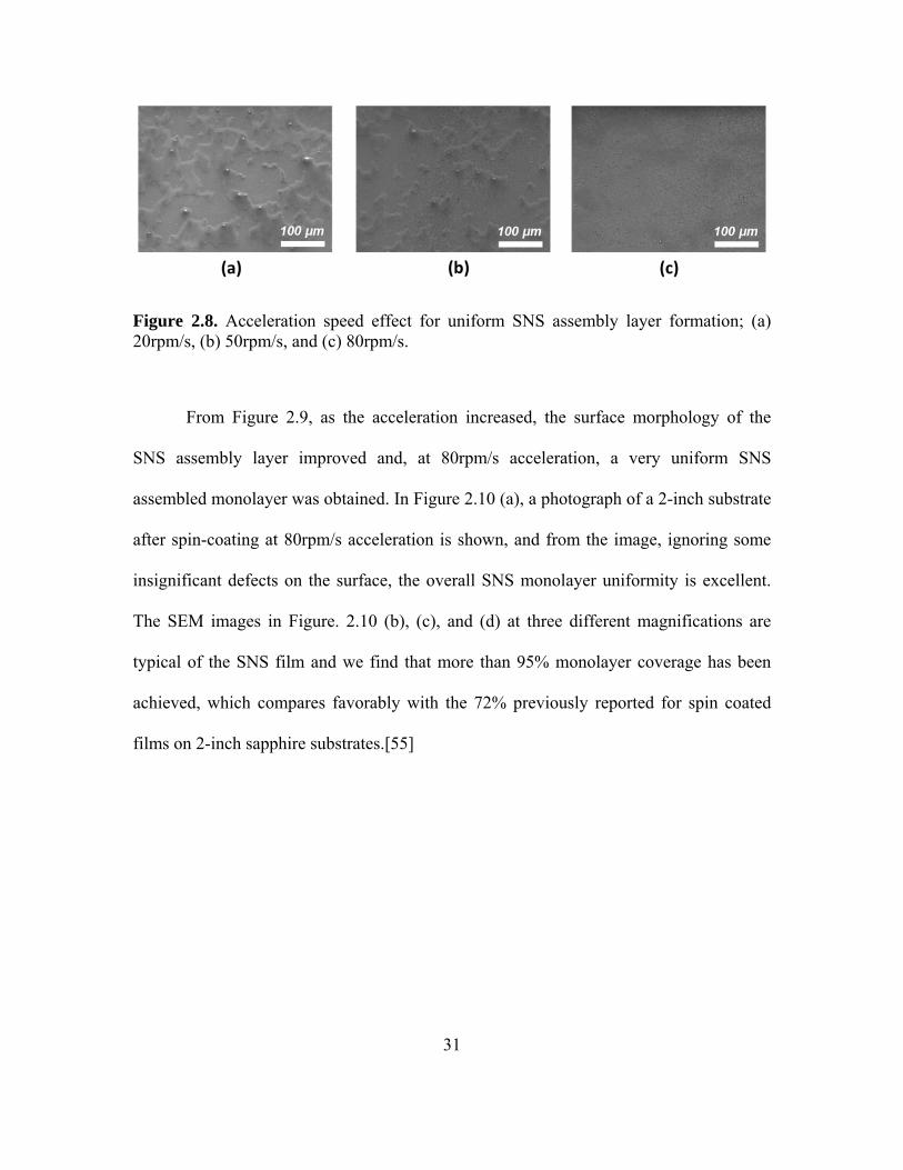
From Figure 2.9, as the acceleration increased, the surface morphology of the
SNS assembly layer improved and, at 80rpm/s acceleration, a very uniform SNS
assembled monolayer was obtained. In Figure 2.10 (a), a photograph of a 2-inch substrate
after spin-coating at 80rpm/s acceleration is shown, and from the image, ignoring some
insignificant defects on the surface, the overall SNS monolayer uniformity is excellent.
The SEM images in Figure. 2.10 (b), (c), and (d) at three different magnifications are
typical of the SNS film and we find that more than 95% monolayer coverage has been
achieved, which compares favorably with the 72% previously reported for spin coated
films on 2-inch sapphire substrates.[55]

32
Figure 2.9. (a) SNS deposited 2-inch round Si surface image, and the SEM images with different magnifications, (b) 250x, c) 2000x, and (d) 25000x, respectively.
Furthermore, we also tested 4-inch round substrates to investigate the feasibility
of DMF for SNS assembled monolayer spin-coating on an even larger-scale surface area
using the identical spin-coating recipe and SNSDMF concentration. The only parameter
changed was the dispensed solution volume which was 800μl (300 μl for 2-inch) to
compensate for the increased surface area. As shown in the photograph and SEM images
in Figure 2.11, we found that the DMF based solution performs well on larger substrates
with more than 90% averaged monolayer coverage achieved on 4-inch wafers with good
monolayer uniformity. For 4-inch wafer spin-coating, however, there were some less
SNS covered (76~88%) areas observed as shown in Figure 2.11 (c).

33
Figure 2.10. (a) SNS deposited 4-inch round Si surface image, SEM images of (b) low magnification, (c) less SNS monolayer coverage region of blue solid-box in (b), and (d) high SNS monolayer coverage region of red solid-box in (b).
Based on our experiments (see Figure 2.8), the appearance of this reduced
coverage area is typical when the solution concentration was not optimal and therefore
we believe that the coverage can be further improved by adjusting the solution
concentration. However, even without further optimization, we credit as a rare success
the SNS spin-coating of a 4-inch wafer at this level of monolayer coverage and
uniformity without special environment controls or additional surface
functionalization.[59]

34
2.1.8. Spin-Coating of SNS in Various Diameters: Diameter vs. SNS Solution
Concentration
In this section, we also demonstrate the effectiveness of our DMF introduced
spin-coating method to deposit SNS with various diameters. Three different sizes of SNS
(310, 600, and 840 nm in diameter) are tested to observe the relation between SNS
diameter and concentration to produce maximum SNS monolayer coverage (>95%) on 2-
inch Si wafer surface. In Figure 2.26 (a) ~ (c), photographs and SEM images of three 2-
inch Si wafers are shown with three different SNS sizes: 310, 600, and 840 nm in
diameter, respectively, and all have more than 95% monolayer coverage.
Figure 2.11. Different size of SNS in (a) 310nm, (b) 600nm, and (c) 840nm diameters, spin-coated on 2-inch Si wafers (Top, middle, and bottom of (a) ~ (c) represent the whole 2-inch wafer with each SNS, ×2k, and ×20k magnification SEM images, respectively.), (d) Optimum SNS solution concentration vs. SNS diameter for spin-coating and (e) table representing the ratio of SNS diameter (Dia., nm) to solution concentration (Conc’, mg/ml) for spin-coating.
35
From the Figure 2.21(d), we observe that the most optimal concentration of DMF
based SNS solution just proportionally increases with the SNS diameter along with its
phenomenal SNS monolayer uniformity. From the Figure 2.21(e), the ratio of SNS
diameter (Dia.) to solution concentration (Conc’) is around “2” for all three diameters of
SNS. Therefore, with our spin-coating method, uniform coatings of various sizes of SNS
are achieved by simply changing the SNS solution concentration based on the SNS
diameter. This provides the user with the capability to control the period (or density) of
fabricated Si nanostructures.
2.1.9. DMF vs. Other Solvents
In addition to DMF, we also tested other solvents for SNS spin-coating such as
dimethyl-sulfoxide (DMSO) which offers a high boiling temperature (189°C), reduced γ
(γDMSO = 43.5mN/m) compared to water (73mN/m), and less toxicity than DMF.
However, its high viscosity (2.0cP at 20°C) produced severe non-uniformity and multi-
layered SNS films after spin-coating as shown in Figure 2.12 (a) and (b). These results
show the importance of each and every solvent property and their combination in
producing uniformly distributed SNS monolayers in close-packed arrays with spin-
coating. Therefore, we believe that, regardless of the toxicity concerns of DMF, it offers
highly optimal solvent properties for large-scale surface area SNS spin-coating
accompanied by outstanding SNS monolayer uniformity and coverage even under
common ambient lab conditions.

36
Figure 2.12. SEM images of DMSO introduced SNS (310nm) spin-coated Si surface which shows (a) severely non-uniform, and (b) multi-layered SNS film. (Note: Spin-coating condition was 80rpm/sec acceleration and 2000 rpm/sec maximum speed for 200-sec)
2.1.10. Summary
We have introduced the use of DMF as a solvent for spin-coating SNS assembled
monolayers on silicon wafers under ambient laboratory conditions without the addition of
surfactants or special surface treatment of the Si. In comparison with the commonly used
solvent, water, it becomes obvious that DMF offers optimal solvent properties for the
SNS spin-coating application. First, DMF leads to highly dispersed SNS in the solution
which is close to the theoretical limit, important in producing a uniform SNS distribution
on the surface. Second, the outstanding wettability of DMF caused by its low surface
tension (γDMF = 25mN/m) at the liquid / solid interface provides superior coverage and
uniformity of the SNS assembled monolayer compared to the same volume and

37
concentration of SNS in water. In addition, the low γDMF also improves the interparticle
interaction since the enhanced wetting of the solution leads to a higher density of SNS
placed near the surface reducing the interparticle distance. Third, the slow evaporation
rate of DMF is desirable for spin-coating applications. Based on these outstanding DMF
properties, we successfully demonstrate excellent coverage with high uniformity of the
SNS monolayer on 2-inch (~ 95%) and 4-inch (~90%) Si substrates. Furthermore,
different sizes of SNS can be coated simply by adjusting the SNS concentration in the
solution which is easily estimated by diameter of SNS. From these achievements, it is
clear that DMF has a great potential for a high-throughput SNS spin-coating application
with simple, and low-cost spin-coating approach to produce highly uniform colloidal
particle monolayer assembly over large-scale surface which can be used as a mask layer
for Si surface nano-lithography.

38
2.2. Surface Nano-patterning
2.2.1. SNS Size Reduction by Reactive-Ion Etching (RIE)
One of major advantages of using SNS for lithography application is that SNS
(i.e., SiO2) can offer stable and uniform etching with plasma assisted dry etch to produce
desired surface pattern size after SNS size reduction. Currently, the most reported
colloidal sphere lithography techniques are based on polystyrene spheres (PS) which it is
highly challenging to produce repeatable size control and well-defined patterns because
of its soft material nature.
Figure 2.13. (a) Spin-coated 2-inch round Si surface images and SEM images of (b) uniformly distributed SS and (c) closely-packed SS shown in different SEM magnifications.
For effective SNS size reduction, there are two criteria to consider; (1) high
enough SNS etching selectivity with Si, and (2) effective horizontal direction etching of
SS with minimized vertical etching rate. The high SNS etching selectivity is important
because excess Si etching during SNS size reduction would affect the shape of target
surface geometry after nanostructure fabrication. Directional selective SNS etching is

39
needed to adjust the lateral dimensions while maintaining sufficient vertical height to
permit clean SNS removal and mask layer liftoff. 1.57um large diameter of SNS was
used to optimize the SNS etching condition due to its relative large size can provide
better visible observation on etching selectivity and orientation. The deposited 1.57um
SNS is shown in Figure 2.13.
Table 2.1. Comparison of CHF3 / Ar gas RIE etching profile for 10-min etching on SS deposited Si surface which were performed under three different chamber pressures.
Pressure Property
50 mTorr 75 mTorr 100 mTorr
Cross-sectional SEM Image
(Scale-bar : 500nm)
Vertical Etching rate
(nm/min) 90.3 80.3 70.3
Horizontal Etching rate
(nm/min) 34.8 30.3 18.1
Vertical / Horizontal Etching ratio
2.6 2.6 3.9

40
Figure 2.14. Schematic illustration (top) and SEM images (bottom) to compare the effect of RIE chamber pressures, (a) as-deposited SS, (b) 75mTorr RIE processed SS (horizontal dia. ~800nm, vertical dia. ~350nm), and (c) 100 mTorr RIE processed SS (horizontal dia. ~800nm, vertical dia. ~260nm).
Based on these considerations, we utilize a CHF3/Ar gas combination in our
process and have optimized its etching conditions by applying different gas flow rates,
RF power, and chamber pressure. From the experiments, we observe that chamber
pressure is the most critical parameter for both of high SNS etching selectivity and low
vertical / horizontal etching ratio. Wide range of chamber pressure was tested, and results
from three different chamber pressures (50, 75, and 100mTorr) are shown in Table 2.1.
With 50mTorr chamber pressure, a noticeable etching of the Si substrate between the
SNS was observed due to intensified ion-bombardment.[66] Therefore, we increased the
chamber pressure to 75 and 100mTorr, resulting in significantly less Si substrate etching
because of the decreased mean-free path of ionized-species. However, even though
higher chamber pressure results in further reduced Si substrate etching, the vertical /
41
horizontal etching ratio (calculated from radius change in each direction after 10-min
etching) listed at the bottom of Table 2.1 increased for 100mTorr. As mentioned before,
this excess etching rate in the vertical direction is not ideal for SNS lithography because a
relatively fast vertical diameter reduction compared to that of the horizontal direction
potentially restricts the choice on the pattern size weakening the ability of the SS to
pattern the surface as SNS size decreases. As shown in Figure 2.13, for the same SNS
target size (~800nm), a higher chamber pressure, 100mTorr in Figure 3(c), produced a
reduced vertical SNS radius compared to that of the lower chamber pressure, 75mTorr in
Figure 2.13(b), due to its relatively faster vertical direction etching. Therefore, 75mTorr
was used for SNS size reduction resulting in acceptable Si substrate etching and
increased flexibility for target pattern size.

42
Figure 2.15. (a) ~ (d) SEM images of RIE etched SS with various etching times, 10-min, 13-min, 16-min, and 19-min, respectively, and (e) diagram of inter-particle spacing (d) versus RIE etching time. (Note: RIE conditions are 75mTorr chamber pressure, 200 Watts RF plasma power at 25/25sccm gas flow rate) (scale bar: 1 um for top image, 500nm for bottom image).
In Figure 2.14, RIE etched 1.57μm SNS is shown with various etching times (10,
13, 16, 19-min) under the optimized RIE conditions. From the SEM images in Figure
2.14 (a) ~ (d), highly effective SNS size reduction was observed with minimal Si
substrate etching. In addition, from Figure 2.14(e), the measured inter-particle spacing
with different etching times showed that SS size can be easily reduced in a desired scale
due to its reasonably linear relation between reduced SS diameter and etching time.

43
Moreover, as observed from Figure 2.14(a) ~ (d) top, after RIE, there was still highly
well-defined circle shape of SNS without any rugged edge which often occurs with soft
PS.[58, 67] Therefore, by using optimal RIE condition with various sizes of SNS, a
highly controlled surface pattern can be produced in a desired period and size.
2.2.2. SNS Removal after RIE
In the previous section, we showed that CHF3/Ar RIE etching can provide
effective SNS selective etching to the Si substrate. However, CHF3/Ar RIE also causes an
issue for SNS removal following mask layer deposition. This is because there is a
formation of a thin CxFy compound layer on all exposed surfaces during the etching
process,[68] and this CxFy compound is highly stable in a hydrofluoric acid based
solution like BOE; as a consequence, clean SNS removal using BOE cannot be achieved
as schematically shown in Figure 2.15(c) and (e) where the red solid-line indicates the
residual CxFy compound layer. In addition, the CxFy also has strong mechanical property;
mechanical SNS removal process (i.e. sonication) is not effective for clean SNS
elimination. (Note: Here, BOE solution etching is used for SNS removal, but later
sonication process is also used to exclude acid involvement during process)
From the illustration and subsequent SEM image in Figure 2.15(e), a sample after
Cr evaporation and BOE etch / liftoff, the CxFy residue results in a collapsed metal mask
layer and incomplete metal liftoff. The SS itself have been etched away by infiltrated
BOE solution. For clean SNS removal from Si surface, therefore, we introduced a simple

44
no-vacuum required UV-ozone (UVO) surface treatment before the Cr evaporation
because of its effective organic contamination removal in a non-aggressive environment.
From Figure 2.15(f) bottom, the SEM image of a sample treated with a 10-min UVO
treatment before Cr evaporation and BOE (10:1) etch shows very clean SS removal from
the Si surface, resulting in well-defined surface patterns.

45
Figure 2.16. Schematic illustration of SNS lithography process and UVO effect to produce clean Si surface patterning, and (e) bottom is SEM image of non-UVO treated sample, and (f) bottom is UVO treated sample. (Green-line indicates deposited Cr layer, and red-line indicates CxFy compound layer on the surface, scale-bar = 1 μm)
2.3. Fabrication of Si NP with Metal-assisted Chemical Etching
In this section, we demonstrate our effective Si nanopillar (Si NP) fabrication
process to produce Si NP with highly well-controlled structural dimension (i.e. period,
diameter, and height). The dimension control of fabricated Si nanostructures in a chosen
period is a key consideration in fields like opto-electronics for effective light diffraction
and/or scattering, [69, 70] which are also highly crucial to realize enhanced light
absorption for thin Si solar cells.
Here, we show our novel fabrication process for Si NPs with control over both
period and dimension. A metal-assisted chemical etching (MaCE) technique is introduced
to provide a fast and low-cost etching process that achieves effective vertical etching with
minimal size variation of the NPs. Various interface metal layers (Cr, Ti, and Ni) are
investigated as Au adhesion layers and Ni is determined to produce enhanced
lithographical accuracy for highly uniform Si NP fabrication of an intended dimension.
Moreover, for MaCE, the influence of fractional catalyst coverage on etch rate and
controlled vertical etching is investigated.

46
2.3.1. Experimental Section
The SNS solution was prepared with powders of 310nm, 600nm, or 840nm
diameter SNS (Bang Lab.) which were dispersed in N,N-dimethyl-formamide (DMF)
(Sigma-Aldrich) at an optimized concentration. The solutions were sonicated for 5 hours
to produce complete dispersion of the SNS.
The test substrates consisted of 2-inch round polished n-type Si (100) wafers
(280μm thickness) cleaned in a piranha solution [H2SO4 (96%):H2O2 (30%) = 4:1] for
15minutes to form a hydrophilic Si surface followed by a 10minute DI-water rinse.
SNSs were spin-coated under common ambient lab conditions at 2000rpm/sec
(80rpm/sec acceleration) for 120 seconds after dropping 300µl of solution on the wafer
surface. The uniformity of SNS spin-coated samples was observed by scanning electron
microscopy (SEM, JEOL XL-30), and the coverage of the SNS monolayer was calculated
by direct counting of the SNS covered area on the Si surface through image analysis
software, “image J” (National Institutes of Health, USA)[71] as shown in our previous
report.[72]
SNS coated Si substrates were then transferred to the reactive ion etching
chamber (Oxford PlasmaLab 80+, RIE) and the SNS size reduction was performed using
a CHF3/Ar gas combination with 200 watts RF plasma power at 25/25sccm gas flow rate
and 75mTorr chamber pressure followed by a 2-min O2 plasma clean with 100 watts at
45sccm gas flow rate and 150mTorr chamber pressure to remove surface organic
contamination resulting from the CHF3/Ar RIE. (Note: The O2 cleaning step after RIE is
highly crucial for later complete SNS removal.) Metal layers for the subsequent MaCE

47
process were deposited with an electron-beam evaporator (Lesker PVD-75); then the
SNS were removed by sonication in water.
The MaCE solution was prepared by mixing 2.5vol% hydrogen peroxide (H2O2)
with 10vol% hydrofluoric acid (HF, 49%) in DI-water. Etching was performed by
immersing samples into the etching solution while stirring. After MaCE, the Au layer
was removed by dipping in Au etchant for 5-min.
2.3.2. SNS Diameter Control with RIE
Here, we measured the etching rate of SNS with various initial diameter which are
shown in Figure 2.17 (310, 600, and 640nm in diameter) to investigate the relation
between etching rate and SNS size. This is because in addition to structure period, the
fabrication of Si nanostructures in a certain dimension is also highly crucial to realize
certain optical property. For instance, the study by Spinelli, et al. has demonstrated that
well-defined Si NPs with optimized period and dimension can offer enhanced forward
scattering of incident light providing an improved omnidirectional anti-reflection effect
over a broad wavelength range.[69] Furthermore, the study by Sang Eon et al.
emphasized the importance of Si nanostructure size (or Si filling fraction) in producing
strong transmitted light diffraction for enhanced light absorption.[73] Thus effective SNS
dimension control is highly crucial to offer highly enhanced optical property for thin Si
solar cell application.
The advantage of using SNS for the NSL process as opposed to widely available
polystyrene sphere (PS) is that SNS (i.e., SiO2) offers sufficient etching selectivity to Si

48
which allows uniform SNS size reduction with an RIE process. Of course, size reduction
of PS is possible, but the soft material nature inevitably produces a non-uniform result;
consequently, the fabricated nanostructure has a rough surface.[74, 75] This rough
surface is especially problematic for surface dominant device application like solar cells
since it generally increases the surface recombination velocity and consequently degrades
solar cell performance.[76]
Figure 2.17. Three different sizes of SNS in (a) 310nm, (d) 600nm, and (g) 840nm in diameter, and RIE etched with two different etch times. (b), (c) are 1.5-min and 2.5-min on 310nm SNS, (e) and (f) are 4-min and 6-min on 600nm SNS, and (h) and (i) are 6-min and 8-min on 840nm SNS. (j) the SNS diameter change vs. RIE time, and (k) a table showing etch rates for each SNS.
In Figure 2.17 (a) ~ (i), plan view SEM images of RIE etched SNS with different
initial diameters prior to and after etching clearly reveal uniform SNS etching retaining a
smooth circular shape. In Figure 17 (j) and (k), the SNS horizontal etching rates are
shown to be relatively constant, ranging from 41.2 ~ 46.5 nm/min as the RIE etching time

49
increases regardless of initial SNS size. Therefore, effective size control of the SNS mask
layer can be achieved with well-defined shapes.
2.3.3. Metal Cathode Layer Deposition for Surface Patterning
The above described SNS nano-lithography technique has been combined with
MaCE technique to fabricate well-defined Si NPs. The MaCE process requires a metal
catalyst layer to reduce the Si surface, forming SiO2 which is etched away by HF mixed
in the MaCE solution. An Au cathode layer was chosen since Au offers a slower etch rate
compared to other noble metals (i.e., Pt, and Ag) and thus provides controllable etching
for Si NPs fabrication.[77] In addition, the process with Au etches Si vertically without a
porous layer formation, and avoids unexpected surface morphology changes.[78] Au,
however, inherently has weak adhesion to the Si surface which is problematic in our
process. After Au layer deposition, a lift off process is used to remove the SNS mask
layer to avoid etching of the Si NPs related to the Au-covered SNS as shown in Figure
2.18 (a). The SNS removal is performed with sonication which leads to Au layer lift-off
from the Si when the adhesion is poor as shown in Figure 2.18 (b). Therefore, an Au
adhesion layer must be introduced and here, three different interfacial metal layers, Cr, Ti,
and Ni, are tested. For the test, 3nm of each adhesion layer is deposited before a 30nm Au
layer deposition. Figure 3 shows SEM images of patterned Au layers with different
adhesion layers taken before and after the 1-hr sonication in DI-water for SNS removal.

50
Figure 2.18. (a) The etched Si nanopillar had un-expected structure damage by in-complete SNS removal due to metal catalyst covered on SNS, and (b) peel-off Au metal layer during SNS removal due to weak adhesion of Au on bare Si surface.
The diameter of the SNS before metal layer deposition was an average of 611nm (Period:
840nm) as shown in Figure 2.19 (a). After SNS removal by sonication, the diameter of
each pattern is measured and as shown in Figure 2.19 (b) ~ (d) with red numbers, Cr and
Ti produced a significantly larger diameter, 722nm and 667nm, respectively, than the
initial SNS diameter, 611nm, but the Ni/Au metal layer combination resulted in an
average pattern diameter of 622nm and this is very close to the initial SNS size.
Therefore, the Ni interfacial layer for Au offers the best lithographical accuracy for Si
NPs fabrication in a desired diameter.

51
Figure 2.19. (a) Si surface with SNS etched to 611nm average diameter (840nm period), (b) Cr/Au, (c) Ti/Au, and (d) Ni/Au deposited Si surface after SNS removal which have 722nm, 667nm, and 622nm diameter of pattern, respectively.
2.3.4. Fabrication of Si NP with MaCE Technique
The MaCE technique is used to fabricate Si NPs since it provides vertical etching
with minimal diameter variation from top to bottom. One of the widely accepted
mechanisms for the MaCE galvanic process is summarized by the two half-cell reaction
below:[74, 79-82]
Cathode reaction at the metal:
H2O2 + 2H+ 2H2O + 2h+ (R1-1)
2H+ + 2e- H2 (R1-2)
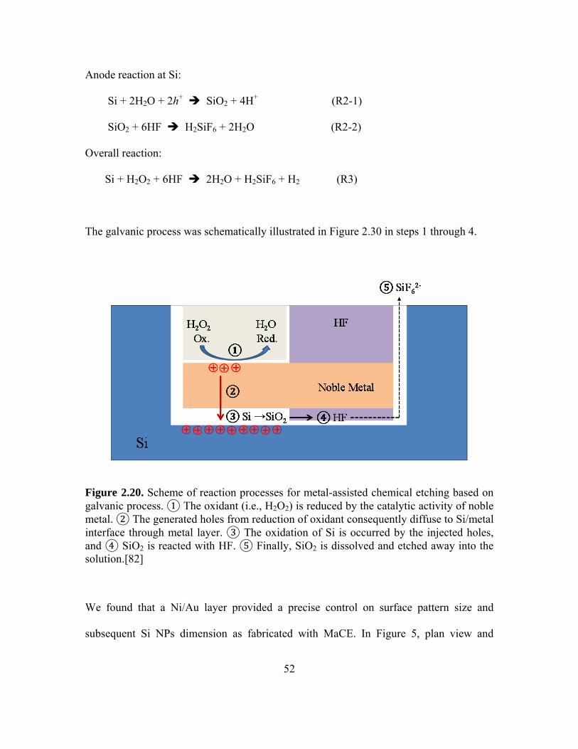
52
Anode reaction at Si:
Si + 2H2O + 2h+ SiO2 + 4H+ (R2-1)
SiO2 + 6HF H2SiF6 + 2H2O (R2-2)
Overall reaction:
Si + H2O2 + 6HF 2H2O + H2SiF6 + H2 (R3)
The galvanic process was schematically illustrated in Figure 2.30 in steps 1 through 4.
Figure 2.20. Scheme of reaction processes for metal-assisted chemical etching based on galvanic process. ① The oxidant (i.e., H2O2) is reduced by the catalytic activity of noble metal. ② The generated holes from reduction of oxidant consequently diffuse to Si/metal interface through metal layer. ③ The oxidation of Si is occurred by the injected holes, and ④ SiO2 is reacted with HF. ⑤ Finally, SiO2 is dissolved and etched away into the solution.[82]
We found that a Ni/Au layer provided a precise control on surface pattern size and
subsequent Si NPs dimension as fabricated with MaCE. In Figure 5, plan view and

53
angled SEM images of three different dimensions of the SNS features and the resulting
MaCE fabricated Si NPs are presented. Figure 21(a), (d), and (g) represents the SNS
etched to 600nm, 445nm and 223nm average diameters (Note: these diameters represent
50% Si filling fraction in the structured layer) arrayed at 840nm, 600nm, and 310nm
periods, respectively. Figure 21(b), (e) and (f) are plan view SEM images and (c), (f) and
(i) are 80 degree angled SEM images of the NPs. The red solid-arrow for each period is
the identical length and indicates good lithographic accuracy.

54
Figure 2.21. (a), (d), and (g) are RIE etched SNS with 840, 600, and 310 nm initial diameter. (b), (e), and (h) are up-side SEM image, and (c), (f), and (i) are 80 degree angled SEM images for Si NPs.
In addition to period and diameter control, a reproducible vertical etching rate for
MaCE is crucial for Si NP fabrication. Therefore, the etching rates with different
fractional Ni/Au catalyst coverage were investigated. Three different fractional coverage
(30%, 50%, and 70%) of the Ni/Au layer, were deposited as shown in Figure 2.22 (a) ~ (c)
and dipped in the MaCE solution for 5-min, with the results as shown in Figure 2.22 (d) ~

55
(f). From the height of the etched Si NP, a gradual increase of etch rate was observed as
the catalyst fractional coverage increased. The plot of the etch rate versus catalyst
coverage indicated that 30%, 50%, and 70% Ni/Au fractional coverage produced 63, 77,
and 104 nm/min etching rates, respectively (see Figure 2.22 (g). The faster etch rate, with
the larger fractional coverage of catalyst, was be explained by enhanced penetration of
etching solution with larger catalyst coverage due to wider inter-spacing between etched
Si NPs. Since the etch depth increases linearly with etch time for MaCE,[82] the etch
times was estimated for a desired height of Si NP. In Figures 2.22 (h) ~ (j), we fabricated
approximately 500 nm height of Si NPs having 70%, 50%, and 30% Si filling fractions in
the structured layer. The Si NPs were produced after dipping in the etching solution for 8-
min, 6.5-min, and 5-min, respectively, which were determined based on the measured
etch rates in Figure 2.22 (g). As a result, fabrication of Si NP in a desired period and
dimension was successfully achieved.

56
Figure 2.22. Ni/Au catalyst deposited Si surface with (a) 30%, (b) 50%, and (c) 70% fractional coverage, and (d) ~ (f) Si NPs fabricated from each catalyst fractional coverage after 5-min etching in MaCE solution. (g) Etch rates from each Ni/Au fractional surface coverage. (h) ~ (j) ~ 500nm height of Si NPs from (a) ~ (c) after dipping in the etching solution for 8-min, 6.5-min, and 5-min, respectively.
In addition, we also confirmed our nano-fabrication process can offer phenomenal
uniformity of farbricated Si NP as shown in Figure 2.23.

57
Figure 2.23. SEM images of fabricated Si NP array at 3 um height in 840nm period (50% Si FF) to confirm the uniformity of the Si NP array over the surface; (a) ×35K, and (b) × 10K magnifications.
2.3.5. Summary
An improved method for fabricating desired aspect ratio Si NPs using silica
nanosphere lithography in combination with metal assisted chemical etching has been
developed. To produce a desired dimension for the SNS mask layer in a fixed period, an
RIE process is used for size reduction of the deposited SNS. Under optimized RIE
conditions, a constant SNS horizontal etch rate regardless of the initial SNS size is
confirmed that retains a well-defined etched SNS shape. For Si NP fabrication, MaCE is
combined with the silica nanosphere lithography technique. Au catalyst layer with Ni
inserted as an Au adhesion layer provides enhanced lithographic accuracy of the metal
mask layer. Further, we were able to observed that the measured etch rates gradually
increase as the fractional coverage of catalyst increases, and successfully estimate the
etch time to produce a desired height of Si NPs with various diameters. As a result, well-

58
controlled Si NPs can be fabricated in a desired period and dimension on large surface
area accompanied by great structure uniformity which potentially provides a powerful
approach to realize enhanced optical and electrical properties of Si for practical
application.

59
2.4. Fabrication of Various Si Micro-/Nano-Structures with Different Etching Techniques
In this section, we also discuss the potential of silica nanosphere lithography
technique for various micro-/nano-scaled Si surface structures fabrication with different
etching techniques like KOH solution etching and reactive-ion dry etching.
2.4.1. Inverted Pyramid: KOH Solution Etching
For the first demonstration of Si surface structure fabrication using our process,
we decided to fabricate an Si inverted pyramid structure which is known to offer effective
light trapping in an optimal subwavelength-scale.[19] In my thesis, we show our result of
~ 1.1 μm scale inverted pyramid with 1.57μm period in a hexagonal array. (Note:
Optically, this is not an optimal scale and density, but is intended to show our capability
to control the size and density of fabricated structure.) To provide a stable masking layer
on the Si surface during the KOH etch, we have chosen Cr mask layer which is
reasonably robust in both BOE and KOH solutions and is a relatively inexpensive metal.
50nm Cr layer was deposited by e-beam evaporation following which the sample was
dipped in BOE (10:1) solution for SS removal. For anisotropic etching of Si inverted
pyramids, a 1% KOH solution was prepared after Si saturation to prevent excess Si
etching and etching was done with 4% IPA addition to improve the etching uniformity.
After KOH anisotropic etching for 2-min at 85°C, a well-defined inverted pyramid
features was observed as shown in Figure 2.24(b) ~ (d). The pattern diameter in Figure

60
2.16(a) was ~1.1 μm, and the resulting inverted pyramid lateral dimension is also
approximately 1.1 μm as shown in Figure 2.16(b).
Figure 2.24. SEM images of (a) Cr deposited Si surface after SNS removal, (b) 1% KOH etched surface with Cr layer, (c) inverted Si pyramid after Cr layer removal, (d) cross-sectional image of inverted Si pyramid, and (e) fabricated inverted pyramid over large

61
surface area to show its uniformity (Inverted pyramid has ~10% size variation likely caused by an initial SNS size variation of 10%.). Note : (a) ~ (d) scale-bar = 1 μm, and (e) scale-bar = 10 μm.
In addition, Figure 2.24(c) ~ (e) showed that our nano-fabrication process can produce
highly uniform inverted pyramid structures over a large surface area with controlled size
and density. Mavrokefalos, et.al demonstrated that the proper scale of Si surface structure
can produce an absorption close to the Lambertian limit in the visible and near IR
regions.[7] Therefore, future size and period optimization for SWSS will be able to
produce broadband absorption enhancement for thin c-Si solar cell applications.
2.4.2. Nano-Pillar & Nano-Tip: Reactive-Ion Etching
Basically, plasma –assisted reactive ion etching (RIE) is the etching method
combining physical and chemical etching which can be done by ion sputtering, and
chemical reaction of radicals with target materials. The basis of RIE is simple; use a gas
glow discharge to dissociate and ionize relatively stable molecules forming chemically
reactive and ionic species and choose the chemistry such that these species react with the
solid surface to be etched to form volatile products. The processes are taking place during
RIE process have been described below,[66] and the processes are schematically
illustrated in Figure. 2.25.
Generation – A glow discharge is used to generate from a suitable feed gas (e.g.
SF6 for Si etching) by electron-impact dissociation/ionization the gas phase etching

62
environment which consists of neutrals, electrons, photons, radicals (F*) and positive
(SF+5 ) and negative (F−) ions.
D.C. bias formation – The Si wafer is placed on an RF driven capacitatively
coupled electrode. Since the electron mobility is much greater than the ion mobility, after
ignition of plasma, the electrode acquires a negative charge, i.e. the D.C. self-bias voltage.
Diffusion/forced convection – The transport of reactive intermediates from the
bulk of the plasma to the Si surface occurs by diffusion. Positive ions from the glow
region are forced to the substrate surface by way of the D.C. self-bias (negative) and will
assist the etching.
Adsorption – Reactive radicals adsorb on the Si surface. This step can be strongly
enhanced by concurrent ion bombardment which severs to produce ‘active sites’ since it
aids in the removal of e.g. the SiFx layer which otherwise passivates the Si surface.
Reaction – A reaction between the adsorbed species and the Si must take place. In
the case of fluorine-based etching of Si, chemical reactions between F atoms and the
surface spontaneously produces either volatile species, SiF4, or their precursors, SiFx (x <
4). However, in Cl-based etching atoms are known to adsorb readily on Si surfaces but
the spontaneous etch rate is very slow. Ion bombardment makes it possible for adsorbed
Cl atoms to attack the backbones of Si more efficiently and form a volatile SiCl4
molecule. This is mechanism is called ion-induced RIE.
Desorption – A desorption of the reaction product into the gas phase requires that
the reaction product is volatile, thus it should have a high vapor pressure at the substrate
temperature. Additionally, there should be no deposited blocking film at the surface. The

63
removal of these films can be greatly accelerated by ion bombardment via sputtering.
This mechanism is known as ion-inhibitor RIE.
Exhaust – The desorbed species diffuse from the etching surface into the bulk of
the plasma and should be pumped out, otherwise plasma-induced dissociation of product
molecules will occur and re-deposition can take place.
Figure 2.25. Schematic illustration of RIE process to etch solid surface.[83]
In our work, the Si surface etching was made with using two major etching
elements which are chlorine (Cl) and fluorine (F). The utilization of these two etching
elements based RIE process can provide more choices on the target shape of surface
texture. F in plasma can offer high reaction probability with Si which is suitable for
isotropic Si etching. In contrast, low reaction probability of Cl can offer highly
anisotropic etching environment producing surface structure with great profile control.

64
Therefore, by combination of F and Cl based RIE processes under various etching
conditions (e.g. gas flow rate, RF power, pressure),[66, 84] the diverse shape of
nanostructures can be fabricated with relatively easy control.
Figure 2.26. Schematic illustration and SEM images to fabricate nanopillar and various aspect-ratio nano-tip structure.
In Figure 2.26, our RIE texturing process has been illustrated with actual SEM
images at each step. As shown in Figure 2.26 (b), the first etching step with ① CHF3/Ar

65
gases is to reduce SNS (SiO2) size to provide etching path for following RIE process, in
addition, to determine lateral size of nanostructure. After SNS size reduction, ② Cl2
(10sccm & 30 mTorr) etching has been made to form nanopillar structure by intensified
anisotropic etching with high RF power (100 watt) as shown in Figure 2.26 (c). Under
continuous ② etching, however, the increased interparticle distance between SNS on top
of Si nanopillar would accelerates the etching rate of Si at top which provides weakened
anisotropic etching producing varied etching rate of Si from top to bottom. With extended
② etching, SNS would be completely removed and the top of Si would be
anisotropically etched to produce dual-scale nanostructure as shown in Figure 2.26 (h). If
there is reduced RF power (50watt) applied under same conditions (③), then, the overall
density and energy of the free electrons would be decreased which produce less negative
D.C. voltage causing further weakened anisotropicity and etching rate; consequently, the
super-sharp nano-tip structure can be fabricated as shown in Figure 2.26 (f). However,
from Figure 2.26 (g), if low-aspect ratio nanotip structure should be made, we can change
gas from Cl2 to SF6/O2 which can provide intensified isotropic etching. (Note: SF6
etching is quite drastic, so should be operated for short period to prevent complete
destruction of texturing). Therefore, the RIE processes with F and Cl based gases can
offer excellent control on Si etching directionality and selectivity to fabricate various
desired Si nanostructures.

66
Chapter 3
OPTICAL SIMULATION FOR SI NANOPILLARS
3.1. Background
3.1.1. Motivation
As briefly mentioned in the introduction, c-Si is an indirect bandgap material
which has a low absorption coefficient especially for long wavelength region (or near-
infrared region). For example, the absorption length will be increased from 10 µm to
about 3 mm in the wavelength range 700 ~ 1100 nm, but this long wavelength region
includes about 41% of photons with energies above the bandgap (Eg) of Si.[20, 85]
Therefore, appropriate optical architecture must be designed for effective light absorption
from long wavelength region to realize high efficiency thin c-Si solar cell fabrication.
In many previous reports, enhanced light absorption with 2-D periodic arrayed
nanostructure has successfully demonstrated computationally and experimentally.[86-91]
This increased light absorption with periodically arrayed nanostructures is attributed to (1)
enhanced anti-reflection (AR) effect from gradual refractive index change or enhanced
photonic behavior for downshifting within nanostructured layer,[92, 93] and (2) increased
fraction of high order transmitted light diffraction.[20, 94] From both of these effects,
highly increased light absorption will be expected by suppressed surface reflection and
increased light path-length in the absorber. However, regardless of their great potential
for enhanced light absorption, their complicated surface geometries including densely
packed and high aspect-ratio nanostructure followed by large surface area enlargement

67
have been main barriers for realistic nanostructure for thin c-Si solar cell application.
Therefore, the complexity of surface geometry must be considered along with optical
property of Si nanostructure.
Therefore, in this chapter, we will investigate the optical properties of Si NPs in
two-dimensional (2-D) periodic hexagonal array fabricated in various geometric
conditions including height, diameter, and period as schematically illustrated in Figure
3.1(a) which can be fabricated by our nano-fabrication process as shown in Chapter 2.
The optical properties of Si NP array are calculated with two different optical modeling
techniques which are rigorous coupled wave analysis (RCWA) and finite-difference time-
domain (FDTD) and methods. RCWA is used to provide a full wavelength-scaled
analysis for incident light scattering behavior and transmitted light diffraction efficiency,
and combination with FDTD successfully provides well-visualized understanding on
overall incident light behavior in different NP conditions. By using these two different
techniques, the optimal geometric conditions of Si NP array for thin c-Si solar cell will be
determined based on effectiveness of resonant scattering in forward direction and
magnitude of transmitted light diffraction at high orders (> 0th order) as schematically
illustrated in Figure 3.1 (b) - (1) and (2), respectively. [93, 94]

68
Figure 3.1. (a) Schematic illustration of simulated Si NP, and (b) investigated optical properties of Si NPs arrayed in 2-D hexagonal formation; (1) forward scattering for reduced front surface reflection loss, and (2) light diffraction order for enhanced light absorption of transmitted light in the absorber.
3.1.2. Rigorous Coupled Wave Analysis (RCWA)
Here for my thesis, RCWA method is used as a main optical modeling technique
to analyze the optical properties of Si NP array due to its less time consuming calculation
process to understand full wavelength-scaled reflection and transmission in addition to its
effectiveness to calculate the diffraction efficiency.
Figure 3.2. Constructed structure to solve a diffraction problem using RCWA. (a) Structure is divided into strata so that each stratum is homogeneous in the z-direction, and (b) horizontally divided strata so that each stratum is homogeneous in the y-direction for circular-shaped structure calculation.
RCWA is a well-known optical simulation technique to calculate the diffraction
behaviors from a periodically arrayed structure. [95-98] Basically, RCWA aims to solve
the equations of light propagation from a homogeneous superstrate through a periodic
medium to a homogeneous substrate as illustrated in Figure. 3.2, RCWA requires that

69
region II in Figure 3.2 (a) is homogeneous in the z-direction. For circular shaped structure,
due to limitation of RCWA for angled shape, the structure is also divided into y-direction
as shown in Figure 3.2 (b). The further theatrical details are shown in reference [99].
Here for my thesis, the commercial software package (GD-Calc), which runs in
MATLAB environment, is used for the RCWA simulations. Incident light was
considered to be randomly polarized by averaging transverse magnetic (TM) and
transverse electric (TE) polarizations.
3.1.3. Finite Difference Time Domain (FDTD)
FDTD is a numerical method where the Maxwell equations are solved by
discretizing time and space.[100] The spatial discretization utilizes a Yee lattice where
the E and H field are stored at intermediate positions to reduce the memory consumption.
The E and H field are then solved in discrete time intervals within the Yee lattice using
the Maxwell equations in partial differential form. The time resolution is usually directly
related to the spatial resolution. FDTD does not require the structure to be periodic, but
periodic, or Bloch wave, boundary conditions may be applied for simulations of waves in
periodic media. The source in an FDTD simulation is an electromagnetic pulse with a
given frequency and duration. The FDTD software computes the E and H field at every
time step until the magnitude of a chosen field component at a given detector position
reaches a certain threshold value. A short pulse length in the temporal domain will result
in a broadening of the frequency spectrum, i.e. one pulse consists of an extended range of

70
frequencies centered on a mean frequency. The response at the detectors may be Fourier
transformed to get spectrally resolved reflection and transmission. In other words, the
response at all frequencies may be computed in only one run. Further details are shown in
reference [101].
Here, I used FDTD to visualize the scattering behavior for Si NP array fabricated
in various geometric conditions to confirm the results of RCWA.
3.2. Design of Si Nanopillar Array with Optical Simulation
3.2.1. Period of Si NPs: Statistical coupled-mode theory (SCMT)
Before we study the specific optical properties of Si NPs with simulation, the
grating period, L, must be determined to accomplish high absorption enhancement over a
broad spectrum range. In previous reports by Yu et.al,[102, 103] the effect of period is
well explained with “statistical coupled-mode theory” based on the number of guided
resonance in a free space and number of resonant channels with incident wavelength.
From the theory, the absorption enhancement factor, F, can reach beyond the
bulk-limit, 4n2, when the normalized frequency, s = L / λ, is comparable or smaller than
“1” which indicates that the period, L, must be comparable or smaller than incident λ.
Based on theory, in case of hexagonal arrayed grating structure, absorption enhancement
beyond bulk-limit, 4n2, when “s” lies between 0.6 and 1.1 as shown in Figure 3.4 below.

71
Figure 3.3. Upper limit of absorption enhancement for a grating with hexagonal lattice periodic structure. Reprinted from Reference [102]
Therefore, if target wavelength region for absorption enhancement is chosen, the
period also can be decided based on that wavelength region. In this thesis, our target
region is longer wavelength since the nano-fabrication process has been developed for
thin-film Si solar cell application which inevitably produces large fraction of light loss in
longer wavelength region. Based on this reason, our target spectral area is 600 to 1100
nm where requires effective light trapping for absorption enhancement; in a consequence,
for our periodic Si NPs in hexagonal array, 600nm grating period (L = 600nm) is chosen
which provides normalized frequency range of 0.54 < s < 1.0 for 600 ~ 1100nm
wavelength region.
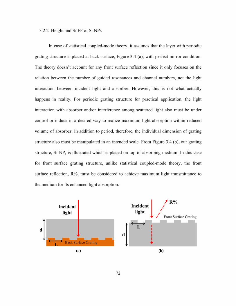
72
3.2.2. Height and Si FF of Si NPs
In case of statistical coupled-mode theory, it assumes that the layer with periodic
grating structure is placed at back surface, Figure 3.4 (a), with perfect mirror condition.
The theory doesn’t account for any front surface reflection since it only focuses on the
relation between the number of guided resonances and channel numbers, not the light
interaction between incident light and absorber. However, this is not what actually
happens in reality. For periodic grating structure for practical application, the light
interaction with absorber and/or interference among scattered light also must be under
control or induce in a desired way to realize maximum light absorption within reduced
volume of absorber. In addition to period, therefore, the individual dimension of grating
structure also must be manipulated in an intended scale. From Figure 3.4 (b), our grating
structure, Si NP, is illustrated which is placed on top of absorbing medium. In this case
for front surface grating structure, unlike statistical coupled-mode theory, the front
surface reflection, R%, must be considered to achieve maximum light transmittance to
the medium for its enhanced light absorption.

73
Figure 3.4. Schematic illustration of grating structured layer for (a) statistical coupled-mode theory, and for (b) our simulation.
Here, we investigate the dimension effect of Si NP arrayed at 600nm period by
introducing different heights and diameters. Since dimension of standing structures at
fixed period is highly crucial in terms of (1) effective confinement of resonant scattering
within structure, and (2) reduced light interference between structures which are directly
related to the magnitude of reflection from the structured surface.[93, 104, 105] In Figure
3.5 (a) ~ (c), the front surface reflection of Si NPs built on semi-infinite thick Si substrate
is calculated with RCWA simulation with three different Si FFs (30%, 50%, and 70%),
and various NP heights from 100 to 400 nm. The FF is defined by the fractional area of
Si NP and each FF of 30%, 50%, and 70% FF are equivalent to 344, 444, and 520 nm in
diameter, respectively. From the Figure 3.5 (a), 30% FF at 200nm Si NP height (red-line)
reveals highly suppressed front surface reflection, especially in the 600nm ~ 1100nm
wavelength range compared to other aspect-ratio Si NPs. However, even with same
height, as FF increases, overall reflection from front surface increases. In Figure 3.5 (d),
the weighted reflection are shown separately for short (300 ~ 600nm) and long (600 ~
1100nm) λ region in different NP heights and FFs. From the Figure 3.5 (d), for long λ
region, the front surface reflection can be very effectively suppressed for both of 30%
and 50% FFs at 200nm height, but 30% FF can also provide enhanced AR effective to
suppress reflection from short λ region compared to 50%.

74
Figure 3.5. RCWA results for front surface reflections from three different Si FFs, (a) 30%, (b) 50%, and (c) 70% representing 344, 444, and 520 nm Si NP diameters, respectively, and the height range is from 100 to 400nm with 100nm interval. In addition, (d) reflection trends for short (300~600nm) and long (600 ~ 1100nm) λ are shown with different NP heights in weighted reflectance. (Note: Period is fixed at 600nm)
Therefore, well-optimize Si NP in volume represented by Si FF (NP diameter) and height
can produce suppressed reflection despite of its low-aspect ratio. Typically, the AR effect
gets intensified with higher aspect-ratio of nanostructure, so this highly suppressed
reflection at lower aspect-ratio (30% FF at 200nm height) compared to other high aspect-
ratio Si NPs cannot be explained only with AR effect of NP.

75
To understand the resonant scattering behavior with various Si NP dimensions,
FDTD simulation also has been performed due to its effectiveness to analyze certain
optical phenomena with visualized results. In Figure 3.6, height effect has been simulated
at 30% fixed Si FF (344nm in diameter) with 900nm incident λ.
Figure 3.6. Incident light scattering behavior (λ = 900nm) with various heights; (a) 100nm, (b) 200nm, (c) 300nm, and (d) 400nm at 30% fixed Si FF
From the results, as the increases from 100nm to 200nm, highly well-confined
scattering behavior is observed within 200nm NP. In addition, the magnitude of
scattering is also stronger at 200nm compared to 100nm NP. However, in case of taller
NPs, 300nm and 400nm, even though stronger intensity of scattering within NPs is still
observed, we also found that confinement of light scattering within NP is getting
weakened with these taller NPs which can attribute to scattered light interference inside
NPs is also getting significant due to increased density of state with taller Si NP. [106] As
a result, electric field distribution above the structured surface is getting noticeable
indicating large fraction of back reflection occurred with taller NP above 200nm.
Furthermore, the increased intensity of electric field between NPs taller than 200nm
represents the weakened confinement effect for resonant scattering with taller NPs due to

76
excess scattered light interference. From the same reason, in Figure 3.7, we also observe
that increased back reflection as NP FF (or diameter) increases from 30% to 70%.
However, in case of diameter, because of increased NP volume to lateral direction, the
interferences are also getting dominant horizontally.
Figure 3.7. Incident light scattering behavior (λ = 900nm) with various Si FF; (a) 30%, (b) 50%, (c) 70% at 200nm fixed height
These increased light interferences are confirmed by Figure 3.8 (a) and (b) which shows
red-shifting of front surface reflection as FF (or diameter, at 100nm height) and height (at
70% FF) increases. We know that downshifting of light is natural phenomenon with
secondary light scattering (or interference).

77
Figure 3.8. Red-shifting of front surface reflection as (a) FF (or diameter, at 100nm height) and (b) height (at 70% FF) increases.
From the RCWA and FDTD simulations, it is very obvious that well-defined NP
dimension is highly crucial to produce effective incident light confinement within the NP
volume producing maximum light transmittance to the medium for absorption. From the
simulations, we found that, for 600nm period, the 200nm height and 30% FF (344nm in
diameter) are the desired Si NP dimensions in our conditions.
3.2.3. Diffraction Efficiency of Transmitted Light
From previous sections, we mostly focused on the light scattering behavior on
front surface with various aspect-ratio Si NPs to produce suppressed front surface
reflection. In this section, the grating effect of Si NP will be studied for large fraction of
high order transmitted light diffraction. As illustrated in Figure 3.9, the effective light
absorption in the longer λ region requires reduction on both of front and back surface
reflection. For maximum light absorption in the longer λ region, the transmitted light
path-length must be increased due to dramatically increased absorption length of light in
longer λ region as discussed in the introduction.

78
Figure 3.9. Schematic illustration of light loss mechanisms for incident light in short (blue arrow), and long (red arrow) wavelength region
With plain Si surface or large-scale surface structures larger than incident
wavelength, 0th order transmitted light diffraction is dominant due to no or weak grating
effect with those surface geometric conditions. In Figure 3.10 (a), it is shown that bare Si
surface produce no specific direction of transmitted light scattering and Figure 3.10 (b)
shows that total transmitted light is transmitted to Si substrate with 0th order diffraction
which is just normal to the incident surface. Therefore, the transmitted light path-length
for absorption will have its shortest; in a consequence, large back-surface reflection loss
will be un-avoidable as illustrated in Figure 3.9 with red arrow (2).

79
Figure 3.10. Optical simulation for transmitted light orientation with (a) FDTD (λ = 1000nm), and (b) RCWA
Here, fractional diffraction efficiency at higher order above 0th with 2-D
hexagonal arrayed Si NPs is calculated with RCWA for same NP conditions from Figure
3.5. This calculation is done to investigate grating effect of each NP to produce large
fraction of high order transmitted light diffraction as illustrated in Figure 3.11.
Figure 3.11. Schematic illustration of grating effect with Si NP to produce high order transmitted light diffraction

80
In Figure 3.12, along with enhanced forward scattering of 30% FF, Si NP in 30%
FF also produces larger fraction of transmitted light diffraction above 0th order compared
to 50%, and 70% FF. The overall decrease of high order diffraction with larger diameter
can be attributed to reduced amount of total transmitted light from longer λ as shown in
Figure 3.5 (d) with solid-line. The height effect on high order diffraction can be explained
by light inferences after resonant scattering. For instance, in Figure 3.12 (a) for 30% FF,
the overall increase of high order diffraction from 100 nm to 200nm is originated from
stronger scattering producing no or insignificant light interferences as shown in Figure
3.6 (b). However, with 300nm NP height, we observed that 700 ~ 900 nm λ has reduced
high order diffraction in contrast to spectral region above 900nm showing increased
fraction of high order diffraction. As shown in Figure 3.6(c), dominant direction of
scattered light is forward direction to the substrate which indicates that red-shifted
incident λ after scattering is involved in increased high order diffraction; in a
consequence, imbalance in high order diffraction over the spectral range is produced. In
case of 400nm NP, as shown in Figure 3.5(a), for 400nm, there is highly increased front
surface reflection in 700 ~ 1100nm λ since excess light interferences are occurred within
400nm NP producing intensified back scattering. From Figure 3.6 (d), increased back
scattering within NP is shown as height increases from 300nm to 400nm producing more
surface reflection of red-shifted incident λ. It is clear that larger Si NPs generally produce
reduced fraction of high order diffraction which indicates its weakened grating effect
with large FF of Si NP array.

81
Figure 3.12. Fraction of high order (>0th) transmitted light diffraction with (a) 30%, (b) 50%, and (c) 70% Si FF at various height from 100nm to 400nm
This weakened grating effect is because even though the period is fixed at 600nm,
larger diameter (or FF) of Si NP provides increased volume for light scattering which
produces more light loss from the surface by scattered light interferences which we
already discussed in Figure 3.7. In Figure 3.12, the total T% with 1 µm thick Si substrate
with 30%, 50%, and 70% FF of Si NP arrays is calculated and as FF increases, the
fraction of transmitted light is decreased which is because of increased back scattering.
Therefore, along with highly increased transmitted light, 30% FF & 200nm also provide
most effective NP dimension to produce high order light diffraction in the absorbing
medium, Si.
3.2.4. Absorption Enhancement of Si NP array
The absorption with Si NP arrayed 5 um thick Si substrate is also calculated with
ideal NP conditions (30% FF, 200nm height at 600nm period) which compares with bare
Si surface. In Figure 3.13, from the comparison with bare Si surface representing L >> λ,
Si NP arrayed Si surface (L is comparable or slightly smaller than incident λ) offers

82
highly enhanced light absorption right above 580nm to 1100nm. This spectral region is
where we plan to increase absorption with 600nm period based on “statistical coupled-
mode theory” in the beginning of this chapter.
Figure 3.13. RCWA results for reflection of Si NP fabricated at 30% FF, 200nm height and 600nm period and reference reflection from bare Si surface (5 µm thick Si substrate). Both surfaces have back reflector (BR, 200nm in perfect mirror condition) and front anti-reflection layer (AR, 70nm SiNx).
Therefore, for highly enhance light absorption with periodically arrayed grating structure
on the front surface, having optimal scale of diameter and height is also highly crucial to
produce light absorption in the interest spectral region.

83
3.2.5. Summary
In conclusion, from the RCWA and FDTD optical modeling, we found that
600nm period, 30% FF, and 200nm height are the most ideal geometric condition for Si
NPs arrayed in 2-D hexagonal formation. This is because this physical condition of Si NP
produces significantly suppressed front surface reflection and most enhanced grating
effect for enhanced light absorption especially for the longer λ region where requires
highly increased absorption length compared to shorter λ; in a consequence, the NP array
in this dimension at 600nm period can provide great potential for thin c-Si solar cell
application.
In addition, the simplicity of surface geometry of our Si NP potentially offer a
lower barrier to fabricate high efficiency nanostructure thin Si solar cell since it provides
improved compatibility with conventional device fabrication process which are for effect
surface passivation, AR coating, and electrode contact.

84
Chapter. 4
FABRICATED SI NP BASED ON OPTICAL MODELING
In previous chapter, RCWA and FDTD optical simulations had been performed to
find the ideal geometric conditions for Si NP array which is potentially applicable for hgh
efficiency thin Si solar cell. In chapter 2, we also demonstrated that our capability to
produce Si NP in various periods and dimension arrayed at hexagonal formation with
enhanced lithographical accuracy. Therefore, in this section, comparison between
experimental and computational results for Si NPs will be made to show the accuracy of
our nano-lithography and nano-fabrication process to realize control period and
dimension of Si NP to produce simulated optical property.
4.1. Demonstration of Simulated Si NPs
4.1.1. Fabricated Si NP vs. Simulated Si NP
The simulated Si NPs in Chapter 3 are experimentally fabricated with SNS
lithography technique after combined with MaCE process which we already showed in
Chapter 2. For comparison of computational and experimental results, 600nm period and
30% FF of Si NPs are fabricated and the reflectance trend has been studied for various
heights to confirm the effectiveness of low aspect-ratio Si NP to suppress the surface
reflection. In Figure 4.1, the fabricated Si NPs (600nm period, 30% FF) are shown for
various heights from 100nm to 400nm.

85
Figure 4.1. Fabricated 30% FF Si NPs in 600nm periodic hexagonal array approximately for (a) 100nm, (b) 200nm, (c) 300nm, and (d) 400nm heights
After Si NP fabrication, deposited Au catalyst layer (30nm) is removed by
dipping the samples in gold etchant solution to measure accurate reflection (R%) from Si
NP fabricated Si surfaces. In Figure 4.2, the measured surface R% is shown and from the
results, it is clear that 200nm Si NP (red-line) produces the lowest surface R% compared
to others. This suppressed R% with 200nm height at 600nm period and 30% FF is well
matched with previous computational result as shown in Figure 3.6 (a).

86
Figure 4.2. Measured reflectance of Si NPs at different heights
The surface reflection from fabricated Si NPs is also compared with optical
modeling results as shown in Figure 4.3. From the Figure 4.3 (a) and (b) for 100 and
200nm NP heights, pretty well-agreed reflection behaviors are obtained, but with 300 and
400nm heights, there is noticeable increased mismatch between measured and calculated
results. We believe that this mismatch is because as height increases, the light scattering
with Si NP gets complicated due to significantly increased light interference as shown in
Figure 3.6; in a consequence, accurate optical simulation for taller Si NP array is more
challenging.

87
Figure 4.3. Comparison of surface reflection between computational (RCWA, dash-line) and measured (Measured, solid-line) reflection for (a) 100nm, (b) 200nm, (c) 300nm, and (d) 400nm Si NP heights (Measured Si substrate thickness = 280 µm and RCWA simulated Si substrate thickness = semi-infinite)
However, despite the some mismatch with higher aspect-ratio Si NPs between
calculated and measured reflection, the overall reflection trend is pretty well matched
between them. In Figure 4.4, we compare the trend of weighted reflection, RW, for whole
(300 ~ 1100nm), short (300 ~ 600nm) and long (600 ~ 1100nm) λ region between
measured and RCWA simulated results.

88
Figure 4.4. Comparison of measured (Red solid-triangle) and RCWA simulated (blue solid-diamond) weighted reflection change for (a) whole wavelength range (300 ~ 1100nm), (b) short (300 ~ 700nm) and (c) long (700 ~ 1100nm) λ region with increasing Si NP height
From Figure 4.4 (a), the whole wavelength range from 300nm to 1100nm, as we
observed from Figure 4.3, the trend of RW starts to be mismatched with Si NPs taller than
200nm. The measured RW keeps decreasing as height increases but the RCWA simulated
RW reveals the highest RW for 300nm and the lowest for 400nm height. From Figure 4.4
(b) and (c) for short and long λ region RW, the short λ region is the problematic region to
cause this RW mismatch since the long λ region produces quite well-agreed trend between
two results. We believe that this RW mismatch for short λ can be attributed to increased
structure damage for taller Si NPs. In Figure 4.6, the damage on Si NP is shown in red-
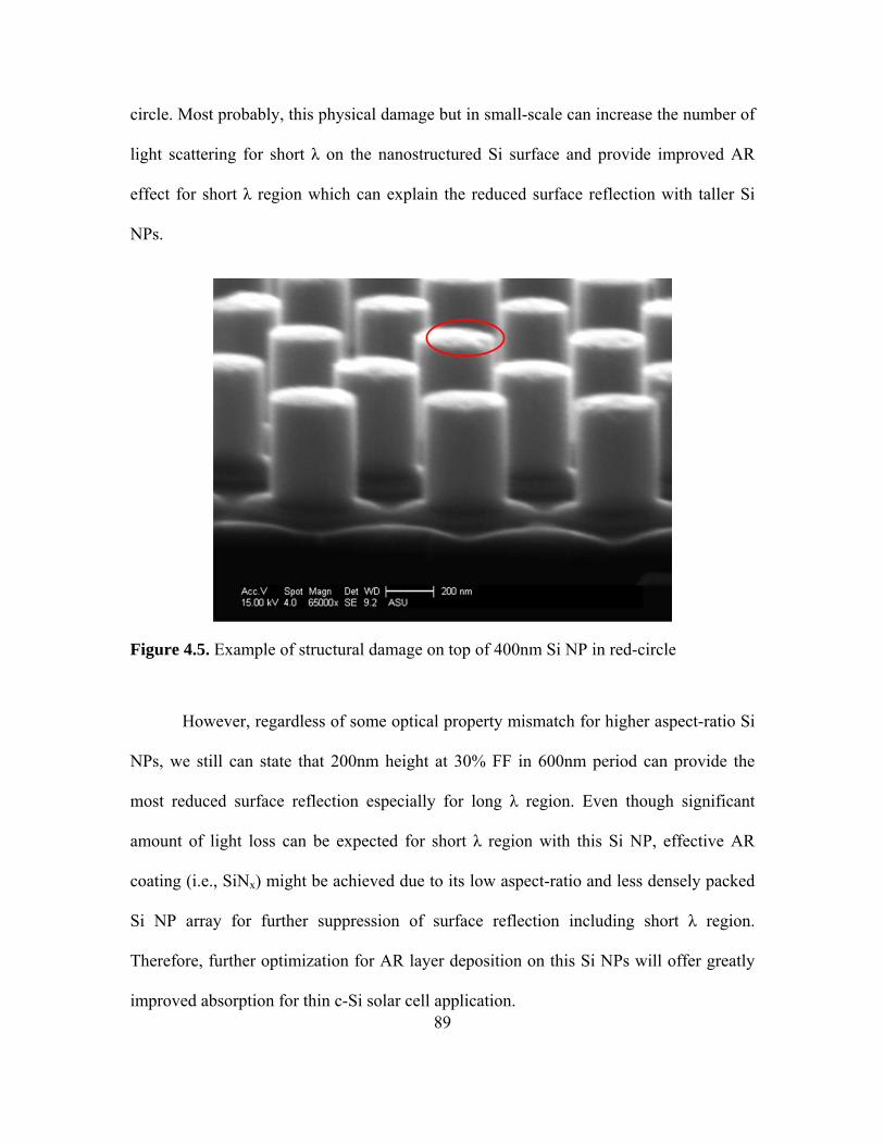
89
circle. Most probably, this physical damage but in small-scale can increase the number of
light scattering for short λ on the nanostructured Si surface and provide improved AR
effect for short λ region which can explain the reduced surface reflection with taller Si
NPs.
Figure 4.5. Example of structural damage on top of 400nm Si NP in red-circle
However, regardless of some optical property mismatch for higher aspect-ratio Si
NPs, we still can state that 200nm height at 30% FF in 600nm period can provide the
most reduced surface reflection especially for long λ region. Even though significant
amount of light loss can be expected for short λ region with this Si NP, effective AR
coating (i.e., SiNx) might be achieved due to its low aspect-ratio and less densely packed
Si NP array for further suppression of surface reflection including short λ region.
Therefore, further optimization for AR layer deposition on this Si NPs will offer greatly
improved absorption for thin c-Si solar cell application.

90
4.1.2. Si NP vs. Conventional KOH Pyramid
To confirm the increased light absorption of geometrically optimized Si NP array,
the surface reflection from our Si NP array and conventional KOH random pyramid is
made as shown in Figure 4.6. The KOH pyramid is chosen since it can represent the
surface structure from conventional ray-optic approach having L >> λ. If it is true that our
optimal Si NP array fabricated in 600nm can provide enhanced light absorption beyond
bulk-limit, 4n2, for 600nm ~ 1100nm spectral range where we plan initially, the surface
reflection from Si NP arrayed surface must be lower than KOH pyramid textured surface.
Figure 4.6. Comparison of surface Reflection between Si NPs (Red solid-line, 200nm height, 30% FF, and 600nm period) and conventional KOH solution etched random pyramid (Black solid-line) fabricated on 280um Si substrate.
In Figure 4.6, from the measured surface reflection for both surface structures, as
we expected, Si NP arrayed Si surface provides significantly suppressed surface
reflection for longer λ region (580nm < λ < 1100nm) compared to KOH pyramid. The

91
absorption enhancement is observed from 580nm, not 600nm since the Si NP array
fabricated in hexagonal formation which can provide wider frequency range for
absorption enhancement compared to square lattice structure. This is because wavevector,
k, of hexagonal lattice structure is slight large than that of square lattice. More
explanation about the effect of lattice structure is further explained in Appendix section
for “statistical coupled-mode theory”.
4.1.3. Summary
From the comparison of results between computational and experimental works,
highly increased light absorption for target wavelength region can be achieved by
introducing a proper scale of period and optimal dimension of Si NPs including diameter
and height. From the results, we confirm that Si NP array fabricated at 30% FF and
200nm height in 600nm hexagonal array can provide absorption enhancement beyond
bulk-limit for target spectral region (600 ~ 1100nm).

92
Chapter. 5
ORGANIC PASSIVATION FOR SI SURFACE
5.1. Understanding of Molecular Contribution for Effective Quinhydrone/Methanol
Organic Passivation for Silicon
5.1.1. Fundamental of Recombination Processes
Whenever the thermal-equilibrium condition of a semiconductor system is
disturbed (i.e., pn ≠ ni2 where p = hole, n = electron, and ni = intrinsic carrier
concentration) by any external excitation, processes exist to restore the system to
equilibrium (i.e., pn = ni2). These processes are recombination when pn > ni
2. And can
occurs both in the bulk and at the surface of the semiconductor system. This
recombination process is problematic especially for photovoltaic device since photo-
generated excess carriers (i.e., e-h pair) can be lost due to recombination processes before
being extracted to the external circuit. During recombination, photo-generated electrons
in the conduction band fall back to the valance band; in a consequence, recombination
between the electron and hole will be occurred, and the excess carrier concentration in
the semiconductor system eventually reaches its equilibrium level. For PV system, if it
has a high recombination rate, the photo-generated current (Jsc) would be dropped and
subsequently, open circuit voltage (Voc) would be decreased by Eq. 5.1. Higher rate of
recombination increases the magnitude of saturation current (J0) followed by overall
device efficiency drop by Eq. 5.2.

93
ln 1 5. 1
∙ ∙
5. 2
Therefore, sufficiently long carrier lifetime (τ) must be achieved for effective photo-
generated carrier collection before recombination. The τ is a function of excess carrier
density, ∆n, and net recombination rate, U, given by Eq. 5.3.
τ ∆
5. 3
From Eq. 5.3, higher τ can be achieved by offering reduced net recombination (U)
to semiconductor system which relies on different recombination processes occurring in
the bulk and the surface of the semiconductor system. The recombination is basically
originated by;
- Shockley Read Hall (SRH) recombination via defects in the band gap
- Radiative recombination
- Auger recombination
- Surface recombination

94
Figure 5.1. Carrier recombination mechanism in semiconductor system.[107]
SRH recombination: SRH recombination is the process directly related to
impurities or crystal defects of semiconductors.[108] In this process, the e-h pairs
recombined through the defects or impurities which act as deep trap states lying within
the forbidden band. These deep trap states can effectively facilitate a two-step
recombination process where conduction electrons can relax to the defect level and then
relax to the valence band, annihilating a hole in the process. Therefore, the SRH
recombination is mainly dependent on the density of trap states (NT), their energy levels
(ET) within the band gap, the capture cross-sections of electrons (σn) and holes (σp). The
SRH recombination rate, USRH, is given by Eq. 5.4.
5. 4

95
where, n = n0 + Δn and p = p0 + Δp (n0, p0 are the equilibrium carrier concentration and
Δn, Δp are the excess carrier concentration), τp and τn are the lifetime parameters (for
hole and electron, respectively) whose values depend on the type of trap and the volume
density of trapping defects given by Eq. 5.5 and n1, p1 are the parameters that introduce
the dependency of the recombination rate on the trapping energy level, ET, given by Eq.
5.6.
1
1
5. 5
exp exp 5.6
Therefore, using the relation between τ and U given in Eq. 5.3, SRH lifetime can be
given by Eq. 5.7.
∆
5.7
where, p0 and n0 are carrier concentration for equilibrium condition.
Radiative recombination: For radiative recombination, Band-to-band
recombination occurs when an electron moves from its conduction band state into the
empty valence band state after releasing the excess energy in the form of photon.
Radiative recombination process directly opposite to carrier generation process occurred
96
by introducing external energy to the system (i.e., incident light). During the radiative
recombination process, the excess electrons in the conduction band fall back to the
valence band and recombine with holes. The radiative lifetime, τrad can be given by Eq.
5.8.
1
∆5. 8
where, B is the radiative recombination coefficient. For silicon, B = 4.73 × 10 -15 cm3/s at
300 K. The radiative recombination is more prevailed in direct bandgap semiconductors
like GaAs and in case of silicon the radiative recombination rate is extremely small due
to its indirect band-gap where phonon emission is dominant instead of photon.
Auger recombination: For Auger recombination process, an electron and a hole
recombine in a band-to-band transition, but now the resulting energy is given off to
another electron or hole. The involvement of a third particle affects the recombination
rate so that we need to treat Auger recombination differently from band-to-band
recombination. The Auger lifetime is given by Eq. 5.9.
1
2 ∙ ∆ ∆ 2 ∙ ∆ ∆5. 9
where, Cp and Cn are Auger recombination coefficient for holes = 1 x 10-31 cm6/s and for
electrons = 2.8 x 10⁻³¹ cm6/s, respectively. From Eq. 5.9, we can see that τAuger is

97
inversely dependent on ∆n2 which implied that for heavily doped substrates or under high
carrier injection conditions, τAuger will be the limiting factor for overall carrier lifetime.
Surface recombination: For semiconductor materials, recombination at surfaces
and interfaces can have a significant impact on the behavior of semiconductor devices.
This is because surfaces and interfaces typically contain a large number of recombination
centers because of the abrupt termination of the semiconductor crystal, which leaves a
large number of electrically active states. In addition, the surfaces and interfaces are more
likely to contain impurities since they are exposed during the device fabrication process.
The net recombination rate, Us, due to trap-assisted recombination and generation is
given by Eq. 5.10.
∙
5.10
where, Dit is the interface defect density as a function of trap energy level, ET. nS, pS are
the electron and hole concentration at the surface, respectively and ni is the intrinsic
carrier concentration (for Si, ni = 1 x 1010 cm-3 at 300 K).[109] From the net
recombination rate, Us, the surface recombination velocity, S, can be obtained by Eq.
5.11.
∆
5.11

98
where, ∆ns is the excess carrier density at the surface. When electrical charges are
introduced to the surface by oxidation or depositing dielectric layer, the surface energy
band can be bended to positive or negative direction depending on the polarity of the
electrical charge; in a consequence, the surface exhibits electric field by the surface band
bending which produces carrier imbalance between electron and hole at the surface, and
this phenomenon is called as field effect passivation. Therefore, the effective surface
recombination velocity, Seff can be given by Eq. 5.12.
∆
5.12
where, x = d indicates the length of the space charge region at the surface. Therefore,
effective surface passivation requires a low surface recombination velocity in addition to
low surface defect density.
After considering all of recombination processes above, the effective carrier
lifetime can be given by Eq. 5.13 since carrier lifetime is inversely proportional to
recombination velocity.
11 1 1 1 1
where, τemitter is defined by effective carrier lifetime due to doping level of emitter.

99
5.1.2. Surface Passivation Approaches
There are essentially two approaches to reduce surface recombination to realize
effective surface passivation for semiconductors which are (1) chemical passivation and
(2) field effective passivation. The first, chemical passivation, is to reduce the density of
surface states Dit, through saturation of surface dangling bonds which act as trap state for
carriers. The second, because the rate in Eq. 5.10 is linearly dependent on the product of
the density of electrons and holes at the surface (ns and ps), is to remove one type of
charge carriers from the surface region which can be done using a local electric field,
usually induced by a dielectric material, hosting a large density of fixed charges,
deposited onto the surface, and is referred to as field effect passivation.
5.1.3. Motivation of This Work
Due to many promising applications over a diverse group of electronic devices,
certain specialized organic materials are very much of interest. Ultra-thin organic films
such as self-assembled monolayers (SAMs) are extensively studied due to their potential
to modify the surface electronic properties of metallic and semiconductor materials.[110-
112] Recently, organic molecules or ligands have been used for silicon (Si) surface
passivation, improving the effective carrier lifetime (τeff) and reducing the surface
recombination velocity (SRV) due to the importance of semiconductor surface quality as
discussed in previous sections.[113, 114]

100
High quality passivation of Si is especially important for solar cells which require
minimizing the SRV of photo-generated carriers. Conventionally, dielectric thin films
such as silicon dioxide (SiO2) and silicon nitride (SiNX) are commonly used to provide
effective Si surface passivation. However, the deposition of SiO2 and SiNX typically
requires a high vacuum and/or high temperature process which adds cost to the devices.
The use of organic coatings will reduce cost, and in addition, the rising interest in
nanostructured devices that require ultra-thin and highly conformal passivation layers
further motivates the organic molecular passivation approach.
A large number of studies report organic Si passivation using different organic
molecules,[114, 115] but in most cases insufficient passivation qualities have limited
their further development. However, a quinhydrone/methanol (QHY/MeOH) method
initially developed by Takato [116], has been reported to result in a high τeff (3.3 ms) and
a low SRV (7 cm/sec) at 1.0 E15 cm-3 carrier injection levels with n-type float-zone (FZ)
Si substrates.[117] The simplicity of a Si passivation process in which the sample is just
dipped in a QHY/MeOH solution at room temperature is highly attractive.[118]
Figure 5.2. Molecular structures of (a) BQ, (b)HQ, (c) QHY, (d) SQ (passivation agent).

101
QHY, Figure 5.1 (c), is a very well-known charge-transfer complex between p-
benzoquinone (BQ), Figure 5.1 (a), and hydroquinone (HQ), Figure 5.1 (b), which was
initially studied by Paul et al. in 1980s.[119-122] However, the QHY charge-transfer
complex is also known to be very labile in a solution environment [123, 124] and
previous reports show that QHY exists as various formations of intermediate molecular
radicals in different solvents.[125-127] Because of the instability of QHY in the solution,
QHY itself cannot act as the passivating agent for the Si surface. The study by Cahen et
al. revealed that semiquinone (SQ), Figure 1(d), is the actual passivating molecule
bonding to the Si surface.[128] However, even though the QHY/MeOH passivation
method has been widely studied by research groups, the contribution mechanism of each
molecule (BQ and HQ) and the solvent (MeOH) for Si surface passivation is not clearly
understood. In this thesis we report on the molecular contributions of BQ and HQ in
MeOH to produce effective Si surface passivation in terms of (1) the uniformity of the
passivation layer, and (2) SQ formation.
5.1.4. Experimental Section
To prepare the samples with organic passivation, we used 2-inch × 2-inch squares
cut from n-type FZ Si <100>, 100 Ω-cm resistivity, 450 μm thick double side polished
wafers. The wafers were cleaned in piranha, (H2O2 and H2SO4 mixed in 1 : 4 ratio) for 15
min followed by a 10 min rinse in DI-water and then dipped in a 10 vol% HF solution for
2 min with a 5 min DI-water rinse thereafter. The passivation with BQ/HQ/MeOH

102
solutions was done for 1-hr (if not specified) in a glass beaker sealed by paraffin tape to
prevent solution concentration changes during the process.
Carrier lifetime and AFM measurements were performed immediately after
removal of the samples from the solution and the FT-IR measurements of each solution
were done within 1-hour after the solution was made. The tunneling mode (TUNA) and
high resolution tapping mode AFM (HR-AFM) scans were performed on a Veeco DI-
3100 using a platinum coated conductive probe and super-sharp probe (probe diameter <
2nm), respectively. τeff was measured using a Sinton lifetime tester, WCT-120, in the
quasi-steady state (QSS) mode.
5.1.5. Minority Carrier Lifetime
The minority carrier lifetimes (τeff) with various solution conditions were
measured to distinguish the dominant passivation molecule between the BQ and HQ for
the Si surface. In the measurement of τeff with either BQ/MeOH or HQ/MeOH solutions
(10 mM concentration each), as shown in Figure 5.3 (a), the BQ/MeOH produced ~ 1.7
ms at a 2.0E15 cm-3 carrier injection level, but for the sample with the HQ/MeOH, only
68 µs was measured. From repeated measurements, we found that the τeff of HQ/MeOH
treated samples never exceeded the τeff of the HF pre-cleaned only sample which
indicates that the HQ/MeOH treatment just degrades the SRV of the HF treated surface.

103
Figure 5.3. (a) Measured minority carrier lifetimes (τeff) of BQ (solid-square) and HQ (solid-triangle) treated Si compared to an HF (open-circle) only cleaned sample and (b) the measured τeff at a minority carrier density of 2x1015 cm-3 with 100% BQ, HQ, and various HQ mixture ratios into a fixed 10mM BQ in MeOH.
However, from Figure 5.3 (b), when we measured τeff while varying the HQ ratio
with fixed 10 mM of BQ, the highest τeff, 3.2ms at 2.0E15 cm-3 was achieved at a 1 to 1
mixture ratio of BQ and HQ (1.0 HQ), while with the other BQ : HQ ratios, 1 : 0.5 (0.5
HQ) and 1 : 1.5 (1.5 HQ), a lower τeff of 2.0ms and 1.6ms were measured, respectively.
This result leads us to assume that while HQ has little involvement in the passivation
reaction when it exists alone, it enhances the effectiveness of surface passivation under an
optimal mixture ratio with BQ.
5.1.6. Uniformity of Organic Passivation Layer
In order to understand how HQ is involved in the Si passivation process, the Si
surface morphologies after dipping in the solutions with different HQ mixture ratios were

104
investigated using tapping mode AFM which is a direct way to see the uniformity of the
passivation layer. Because the molecular passivation layer is ultra-thin, the AFM scans
were done with a super-sharp probe (probe diameter < 2nm) to generate high resolution
AFM (HR-AFM) images. The HR-AFM images shown in Figure 5.4 (a) ~ (d) were
obtained from the samples passivated with (a) pure BQ, (b) 0.5 HQ, (c) 1.0 HQ, and (d)
1.5 HQ with 10 mM of fixed BQ.
Figure 5.4. HR-AFM images of (a) pure BQ, (b) 5 mM HQ, (c) 10 mM HQ, (c) 15 mM HQ addition into 10 mM of BQ in MeOH. (Scan scale : 200 nm x 200 nm & scale bar : 50nm)
It is evident that higher HQ ratios produce more prominent molecular islands on
the surface indicating higher molecular density on the surface. However, as shown in
Figure 5.4 (d), the uniformity of the islands deteriorated with the 1.5 HQ mixture ratio.
The cross-section profile for each sample also supports the idea that excess HQ degrades
the uniformity of the passivation layer and this corresponds with the decrease in τeff
shown in Figure 5.3 (b).
To further clarify the influence of HQ for uniformity of passivation layer,
tunneling mode AFM (TUNA) has been also introduced to provide surface conductivity

105
mapping with high current sensitivity (< 1pA). With the TUNA mode AFM, therefore,
we can distinguish the densely packed molecular area (higher conductivity) and areas
where native oxide has formed (lower conductivity) because the passivation layer is not
or only sparsely present. (Note: It is known that the densely packed molecule area on the
Si surface delays formation of native oxide) [129, 130] Examining the TUNA mode AFM
images of surfaces treated with an excess HQ ratio in Figure 5.5 (c), a large number of
dark areas (white circle) were observed on the surface representing areas where rapid
formation of native oxide is allowed corresponding to only localized molecular
passivation when using excess HQ. With lower HQ ratios of 0.5 HQ and 1.0 HQ,
however, fewer dark areas were detected. The large contrast different between 0.5 HQ
and 1.0 HQ can be explained by the different density of SQ produced by H+ exchange
between BQ and HQ since SQ is the actual molecule passivating Si surface as was
confirmed by Cahen et al.[128] From the HR-AFM and TUNA results, therefore, it is
clear that HQ affects the uniformity of the molecular passivation layer on the Si surface.
Figure 5.5. TUNA image of (a) 5 mM HQ, (e) 10 mM HQ, (f) 15 mM HQ addition into 10 mM of BQ in MeOH. (Scan scale : 200 nm x 200 nm & scale bar : 50nm), (Note: It is note-worthy that a 1 to 1 mixture ratio of BQ and HQ might also produce a more ordered molecular stacking of the passivation layer since the higher current flow (or brighter color) at the molecular island region in Figure.5 (b) might indicate that there is a well-

106
ordered pi-pi stacking formation among molecules which improves the conductivity of the molecular layer.[118, 131, 132])
5.1.7. Understanding of Molecular Reaction for Passivation
To better understand the reasons for the variation of passivation layer morphology
and τeff with different HQ ratios, the molecular interaction between BQ, HQ and MeOH
must be clarified. Therefore, FT-IR measurements were taken for the various solution
conditions and Figure 5.6 (a) shows the results including pure MeOH for comparison.
Note in particular the characteristic absorption for the alcohol O-H bond at 3390 cm-1
(stretch) and 1400 cm-1 (bending) which have been marked with vertical lines. BQ in
MeOH produces a highly hydroxyl (O-H) deficient solution since BQ is a strong
oxidizing agent which deprives a hydrogen (H+) from MeOH. Considering that there is
only 10mM of BQ in MeOH, the reaction between BQ and MeOH must be extremely fast
and dynamic since the O-H peaks at 3390 cm-1 and ~1400 cm-1 have nearly disappeared.
(Note: the C-H peak at ~ 2900cm-1 is fairly ubiquitous, so the origin of the C-H peak
intensity change is hard to specify.)[133] Further, FT-IR results showed that the addition
of HQ to the BQ/MeOH solution increased the O-H peak intensity up to the 1 to 1 ratio
with BQ. This is because the oxidation potential of HQ in MeOH is ~ 0.29 V,[82] and
this is lower than that of MeOH itself, ~ 0.38 V.[134] Therefore, when HQ exists with
BQ in MeOH, HQ acts as a strong reducing agent for BQ replacing the role of MeOH as
a H+ donor as shown in Figure 5.6 (c), so a higher fraction of MeOH molecules retain
their H+. In a consequence, the overall absorbance of solution from O-H bonds gradually

107
increased as HQ ratio increases. Above a 1 to 1 ratio the intensity of the O-H peaks at
both 3390 and 1400 cm-1 become saturated which is evidence that only a limited amount
of HQ will react with BQ. This is because the BQ – HQ redox system is known to
produce a stabilized intermediate molecule of semiquinone (SQ) radical by exchanging
one H+ in a non-aqueous and weak hydrogen bonding agent like MeOH.[125] In addition,
from the report by Har-Lavan et al. it was confirmed the final molecular formation
bonding with Si surface is the SQ molecule. In Figure 5.6, the schematic illustration is
shown for SQ formation in the solution to produce Si-SQ bond for passivation.
Figure 5.6. Schematic illustration for SQ formation in solution to produce Si-SQ bonding for Si surface passivation
For SQ formation, only one H+ exchange is required, so 1 to 1 interaction between
BQ and HQ should be the maximum reaction ratio which indicates excess HQ above the
1 to 1 ratio with BQ will remain un-reacted in the solution. In Figure 5.3, it was shown
that HQ alone is not involved in the passivation reaction. Based on the HR-AFM images

108
in Figure 5.4 (d), this un-reacted HQ prevents an intimate interaction between the
passivation molecule and the Si surface thus deteriorating the uniformity of the
passivation layer.
Figure 5.7. (a) FT-IR results of BQ, HQ, and various HQ mixture ratios into fixed BQ in MeOH and pure MeOH, (b) Reducing BQ into one SQ in BQ/MeOH, (c) two SQ formation in BHQ/MeOH.

109
5.1.8. Carrier Lifetime vs. Passivation Time in Solution
We also investigated the effect of treatment time in both pure BQ and BQ : HQ =
1 : 1 (BHQ) in MeOH solutions upon passivation quality using minority carrier lifetime
measurements. Figure 5.7 (a) shows the measured τeff data for Si samples dipped in these
solutions from 10-min to 180-min. A dramatic increase of τeff occurs with BHQ/MeOH
compared to BQ/MeOH for treatment times less than 50-min. This rapid increase of τeff
can be explained by the higher density of SQ in BHQ/MeOH than that of BQ/MeOH
accelerating the reaction rate between SQ and Si dangling bonds. However, a gradual
decrease of τeff with BHQ/MeOH was also observed as the treatment time was further
increased in contrast to the BQ/MeOH solution. From repeated τeff tests for different
treatment times, 1-hr and 3-hr are determined to be the optimal passivation times for
BHQ/MeOH and BQ/MeOH, respectively.
Figure 5.8. Measured τeff of Si samples after dipping in pure BQ and HQ added MeOH solution for 10-min to 180-min.

110
5.1.9. Kelvin Probe Measurement: Si Surface Band-Bending
To help understand the different passivation time effect with BHQ and BQ
solution, the electrical property of passivated Si surface has been investigated by using
Kelvin probe (KP) technique which can measure the variation of surface work-function.
The work-function is extremely sensitive indicator of surface condition which is affected
by absorbed or evaporated layers, surface reconstruction, surface charing, etc. Here, we
used KP system to measure specifically the surface photovoltage (SPV) after organic
passivation. The SPV was measured by comparison the contact potential differences
(CPD) between dark and illumination condition. In Table 5.1, the measured SPV and τeff
for n-type Si substrates with two different surface treatment time in BHQ, BQ, and HQ
solution, 1-hr and 3-hr, respectively.
From Table 5.1, it is obvious that there would be SPV formation with BHQ and
BQ treatment, but no meaningful values of SPV were observed with HQ which has good
agreement with lifetime measurement results. For 1-hr passivation with n-type Si, the
significant SPV has been measured along with increased τeff for both of BHQ and BQ
solution compared to HF pre-cleaned sample. From the SPV results, BHQ and BQ
surface passivation would induce positive (+) charge at Si surface which indicates that
organic molecules offer relatively negative electric charge to the surface.

111
Table 5.1. N-type Si - SPV values (induced charge at Si surface) measured by Kelvin Probe, and τeff & implied Voc measured by photoconductivity decay with various surface treatments & passivation (or dipping) time.
Passivation molecules
Substrate polarity
Passivation time
SPV (meV) (3x10¹⁵)
τeff (μs)
BHQ N 1-hr (+) 314 ± 26 1284
3-hr (+) 249 ± 8 525
BQ N 1-hr (+) 254 ± 13 835
3-hr (+) 317 ± 44 1293
HQ N 1-hr (+) 13 ± 24 68
3-hr (+) 20 ± 22 91
HF N 2-min (-) 70 244
* BHQ Mixture of BQ and HQ in 1 to 1 ratio * n-type : FZ, >100 Ω-cm, <100>, 450μm, DSP
However, after 3-hr extended passivation time, the measured SPV decreases with BHQ,
but that of BQ increases. In addition, as already shown in Figure 5.7, the 3-hr passivation
with BHQ produces degraded τeff in contrast to the improved τeff with BQ solution. From
the comparison between SPV and τeff, results in Table 5.1, it is clear that field effect
passivation is the dominant mechanism for BHQ and BQ organic passivation.[117]
In Figure 5.8, HR-AFM images are shown for 1-hr and 3-hr passivated Si samples
with BHQ and BQ solution passivation which are same samples from Table 5.1.

112
Figure 5.9. HR-AFM images of Si surface after dipping in BHQ [a, b] and BQ solution [c, d] for 1-hr and 3-hr, respectively. (scale-bar = 50nm)
From the Figure 5.8 (a) and (b), 3-hr extended passivation in BHQ/MeOH
produces severe molecular aggregation on the surface, but for BQ/MeOH, the 3-hr
passivation offers more prominent molecular island without aggregation which indicates
BQ produces less dramatic passivation rate compared to BHQ. After analyzing the
morphology, τeff, and SPV from Si samples passivated in various conditions, we can
claim that the surface passivation with BHQ (or BQ) is originated from dipole moment of
absorbed molecules which supports that SPV decreases with increased aggregation of
molecules. This is because, as schematically illustration in Figure 5.10 (a), dipole
moment is a vector quantity produced by charge asymmetry within molecules, but

113
random stacking of molecules in various orientations, Figure 5.10 (b), would encourage
π-π interaction between stacked molecules, reducing magnitude of molecular asymmetry
in a result, producing a weakened dipole moment within the molecular layer. [135]
Figure 5.10. Schematic illustration of (a) SQ in mono-layer, and (b) SQ in aggregation (or multi-layer) producing different degree of molecular dipole moment

114
5.1.10. Summary
Because of the dramatic uniformity change of the passivation layer after HQ
addition, BHQ/MeOH might not be suitable for a complex Si surface geometry which
requires a very uniform and conformal ultra-thin passivation layer. Therefore, depending
on the degree of surface geometrical complexity, adjusting the HQ addition and
optimizing the dipping time is expected to improve the effectiveness of the passivation.
In conclusion, the role of the HQ component of the QHY/MeOH passivation of
the Si surface has been clarified. From the report, HQ alone cannot provide a passivation
effect for Si, but an optimal mixture ratio between HQ and BQ provides a highly
accelerated passivation rate compared to pure BQ due to increased density of SQ after H+
exchange between BQ and HQ in the solution. However, excess addition of HQ causes
severe molecular aggregation and reduced coverage of the passivation layer. Even with
an optimal HQ amount, an excess dipping time also produced a highly non-uniform
surface morphology which, subsequently, degraded τeff. Regardless of its slower
passivation rate, a less dramatic change of passivation layer morphology was observed
with a pure BQ/MeOH solution as dipping time increased, producing a τeff comparable
with BHQ/MeOH. Therefore, pure BQ/MeOH may provide improved passivation for
complex Si surface geometries which require highly conformal and uniform passivation
layers.

115
Chapter. 6
CONCLUSION AND FUTURE WORK
6.1. Conclusion
The objective of this thesis was to develop a fast, cost-effective, and large-area
nano-lithography technique which can also offer enhanced lithographical accuracy to
fabricate Si surface nanostructures with a desired period and dimension. In terms of this
effort, the DMF introduced SNS spin-coating method has been successfully developed,
which provides wide flexibility on pattern size and its period. This is because various
sizes of SNS can be easily deposited by just changing the SNS solution concentration,
which is also predictable based on the diameter of SNS. In addition, uniform and stable
SNS etching with a RIE process produces well-defined and controlled scale of surface
patterns since our optimized RIE provides linear SNS size reduction as the etching time
increases. Our SNS introduced nano-lithography techniques can be combined with
various etching technique like alkaline solution etching, MaCE, and RIE process
depending on the target shape of nanostructures, since different etching techniques offer
different etching properties, like etching direction and selectivity. In this dissertation, we
have successfully demonstrated that nanopillars, nanotips, and inverted pyramids with a
desired period and dimension can be fabricated by using different etching techniques.
In this thesis, we also utilized two different optical modeling techniques which are
the FDTD and RCWA methods. From each computational method, the incident light
scattering and transmitted light diffraction behavior of Si NPs array have been clearly
visualized and understood. From the results of RCWA and FDTD simulation, 600nm is

116
found to be the optimum period of Si NPs in a hexagonal array for both improved AR
properties and grating effects. Furthermore, the physical dimension of Si NP determined
by Si filling fraction and height is also crucial to produce intensified forward scattering
and a large fraction of high order diffraction. As a result, 600nm period, 30% FF, and
200nm height Si NPs are potentially the ideal geometric specification for thin c-Si solar
cell application.
The fabricated Si NPs based on optical modeling results have successfully
produced well-agreed optical property which indicates that our SNS lithography
combined with MaCE can provide highly accurate period and dimension control to
realize the desired optical properties for Si nanostructures.
6.2. Proposed Future Work
In this thesis, we have introduced a novel nano-lithography and fabrication
process by using the SNS lithography technique, which enables the realization of Si
nanostructures with a desired period and dimension. However, our SNS solvent-
controlled spin-coating method is optimized for Si surfaces, not for other material; as a
consequence, the process application for different materials might be challenging.
Therefore, we propose to combine our SNS lithography technique with nano-imprinting
process. The combination of two different technologies can provide a highly accurate
master mold for nano-patterning process, which also can apply for a wide variety of
different applications for different materials. In addition, nano-imprint technology has

117
been widely researched and is presently reaching commercial level. However, the surface
nano-patterning is still highly challenging, which requires time-consuming and expensive
nano-farbication process as we described in the introduction section. Furthermore, the
surface quality where nanostructure is made will be less important with nano-imprinting
process since the SNS monolayer does not have to be deposited.

118
References
1. Becquerel, A.-E., Mémoire sur les effets électriques produits sous l’influence des rayons solaires. Comptes Rendus, 1839. 9(567): p. 1839.
2. Chapin, D., C. Fuller, and G. Pearson, A new silicon p‐n junction photocell for
converting solar radiation into electrical power. Journal of Applied Physics, 1954(25): p. 676-677.
3. Young, A., World Solar Power 2014: Countries Installing Equivalent Of 12
Nuclear Power Plants Worth Of Solar Capacity. International Business Times, 2014.
4. Smalley, R., Our energy challenge. Public Lecture presented at Low Library,
Columbia University, 2003. 23. 5. F., B.J., Episodes. 1989: p. p. 257. 6. Yu, K. and J. Chen, Enhancing solar cell efficiencies through 1-D nanostructures.
Nanoscale Research Letters, 2009. 4(1): p. 1-10. 7. Kamat, P.V., Meeting the clean energy demand: nanostructure architectures for
solar energy conversion. The Journal of Physical Chemistry C, 2007. 111(7): p. 2834-2860.
8. Keeling, C.D., et al., Interannual extremes in the rate of rise of atmospheric
carbon dioxide since 1980. Nature, 1995. 375(6533): p. 666-670. 9. Mann, M.E., et al., Global temperature patterns. Science, 1998. 280(5372): p.
2029-2030. 10. Dresselhaus, M., G. Crabtree, and M. Buchanan, Basic research needs for the
hydrogen economy. 2003, Technical report, Argonne National Laboratory, Basic Energy Sciences, US DOE, http://www. sc. doe. gov/bes/hydrogen. pdf.
11. EPIA, European Photovoltaic Industry Association and Greenpeace, Solar
Generation 6, 2011. 2011: p. www.epia.org. 12. Luque, A. and S. Hegedus, Handbook of photovoltaic science and engineering.
2011: John Wiley & Sons. 13. Green, M.A., Third generation photovoltaics: advanced solar energy conversion.
Vol. 12. 2006: Springer.

119
14. Barnham, K., M. Mazzer, and B. Clive, Resolving the energy crisis: nuclear or photovoltaics? Nature materials, 2006. 5(3): p. 161-164.
15. Herasimenka, S.Y., W.J. Dauksher, and S.G. Bowden, > 750 mV open circuit
voltage measured on 50 μm thick silicon heterojunction solar cell. Applied Physics Letters, 2013. 103(5): p. 053511.
16. Taguchi, M., et al., 24.7% record efficiency HIT solar cell on thin silicon wafer.
2013. 17. Demésy, G. and S. John, Solar energy trapping with modulated silicon nanowire
photonic crystals. Journal of Applied Physics, 2012. 112(7): p. 074326. 18. Campbell, P. and M.A. Green, Light trapping properties of pyramidally textured
surfaces. Journal of Applied Physics, 1987. 62(1): p. 243-249. 19. Mavrokefalos, A., et al., Efficient light trapping in inverted nanopyramid thin
crystalline silicon membranes for solar cell applications. Nano letters, 2012. 12(6): p. 2792-2796.
20. Chong, T.K., et al., Optimal wavelength scale diffraction gratings for light
trapping in solar cells. Journal of Optics, 2012. 14(2): p. 024012. 21. Füchsel, K., et al. Transparent conductive oxides for nano-SIS solar cells. in SPIE
Eco-Photonics. 2011: International Society for Optics and Photonics. 22. Yoo, J., G. Yu, and J. Yi, Black surface structures for crystalline silicon solar
cells. Materials Science and Engineering: B, 2009. 159: p. 333-337. 23. Zhao, J., et al., 24% efficient PERL silicon solar cell: recent improvements in high
efficiency silicon cell research. Solar energy materials and solar cells, 1996. 41: p. 87-99.
24. Tsigara, A., et al., Metal microelectrode nanostructuring using nanosphere
lithography and photolithography with optimization of the fabrication process. Thin Solid Films, 2013. 537: p. 269-274.
25. Burrow, G.M. and T.K. Gaylord, Multi-beam interference advances and
applications: nano-electronics, photonic crystals, metamaterials, subwavelength structures, optical trapping, and biomedical structures. Micromachines, 2011. 2(2): p. 221-257.
26. http://www.ptreb.com/Electron_Beam_EB_Welding_EBW/. 27. http://nanooptics.uni-graz.at/ol/work/m_ebl.html.

120
28. Ganesan, R., et al., Direct nanoimprint lithography of Al2O3 using a chelated monomer-based precursor. Nanotechnology, 2012. 23(31): p. 315304.
29. Han, K.-S., et al., Enhanced performance of solar cells with anti-reflection layer
fabricated by nano-imprint lithography. Solar energy materials and solar cells, 2011. 95(1): p. 288-291.
30. Hirai, Y., et al., Nano-imprint lithography using replicated mold by Ni
electroforming. Japanese journal of applied physics, 2002. 41(6S): p. 4186. 31. Hirai, Y., et al., High aspect pattern fabrication by nano imprint lithography
using fine diamond mold. Japanese journal of applied physics, 2003. 42(6S): p. 3863.
32. Han, K.-S., J.-H. Shin, and H. Lee, Enhanced transmittance of glass plates for
solar cells using nano-imprint lithography. Solar energy materials and solar cells, 2010. 94(3): p. 583-587.
33. Kuo, C.W., et al., Fabrication of Large‐Area Periodic Nanopillar Arrays for
Nanoimprint Lithography Using Polymer Colloid Masks. Advanced materials, 2003. 15(13): p. 1065-1068.
34. Lai, C.-C., et al., Formation mechanism of SiGe nanorod arrays by combining
nanosphere lithography and Au-assisted chemical etching. Nanoscale Research Letters, 2012. 7(1): p. 1-6.
35. Pavesi, L., et al., Optical gain in silicon nanocrystals. Nature, 2000. 408(6811): p.
440-444. 36. Schmidt, V., J. Wittemann, and U. Gosele, Growth, thermodynamics, and
electrical properties of silicon nanowires†. Chemical reviews, 2010. 110(1): p. 361-388.
37. Park, M.-H., et al., Silicon nanotube battery anodes. Nano letters, 2009. 9(11): p.
3844-3847. 38. Geppert, T., et al., Deep trench etching in macroporous silicon. Applied Physics
A, 2006. 84(3): p. 237-242. 39. Kochergin, V. and H. Foell, Novel optical elements made from porous Si.
Materials Science and Engineering: R: Reports, 2006. 52(4): p. 93-140. 40. Huang, Z., et al., Metal‐assisted chemical etching of silicon: a review. Advanced
materials, 2011. 23(2): p. 285-308.

121
41. http://www.mpi-halle.mpg.de/index.html. 42. Tripathi, S.K., et al., Resolution, masking capability and throughput for direct-
write, ion implant mask patterning of diamond surfaces using ion beam lithography. Journal of Micromechanics and Microengineering, 2012. 22(5): p. 055005.
43. Zhao, Y., et al., A flexible chemical vapor deposition method to synthesize
copper@carbon core-shell structured nanowires and the study of their structural electrical properties. New Journal of Chemistry, 2012. 36(5): p. 1161-1169.
44. Chang, P.-C., et al., ZnO nanowires synthesized by vapor trapping CVD method.
Chemistry of materials, 2004. 16(24): p. 5133-5137. 45. http://www.nanowerk.com/spotlight/spotid=7938.php. 46. Jang, H.S., H.-J. Choi, and S.M. Kang, Formation of P-silicon wire by
electrochemical etching using positive photoresist as an etch mask in organic electrolyte. Electrochemical and Solid-State Letters, 2011. 14(8): p. D84-D88.
47. Choi, D.G., et al., Colloidal lithographic nanopatterning via reactive ion etching.
Journal of the American Chemical Society, 2004. 126(22): p. 7019-7025. 48. Jeong, S., et al., Hybrid Silicon Nanocone-Polymer Solar Cells. Nano letters,
2012. 12(6): p. 2971-2976. 49. Hulteen, J.C. and R.P. Vanduyne, NANOSPHERE LITHOGRAPHY - A
MATERIALS GENERAL FABRICATION PROCESS FOR PERIODIC PARTICLE ARRAY SURFACES. Journal of Vacuum Science & Technology a-Vacuum Surfaces and Films, 1995. 13(3): p. 1553-1558.
50. Huang, J.X., et al., Spontaneous formation of nanoparticle stripe patterns through
dewetting. Nature materials, 2005. 4(12): p. 896-900. 51. Hsu, C.-M., et al., Wafer-scale silicon nanopillars and nanocones by Langmuir-
Blodgett assembly and etching. Applied Physics Letters, 2008. 93(13). 52. Denkov, N.D., et al., 2-DIMENSIONAL CRYSTALLIZATION. Nature, 1993.
361(6407): p. 26-26. 53. Wong, S., V. Kitaev, and G.A. Ozin, Colloidal crystal films: Advances in
universality and perfection. Journal of the American Chemical Society, 2003. 125(50): p. 15589-15598.

122
54. Garnett, E. and P. Yang, Light Trapping in Silicon Nanowire Solar Cells. Nano letters, 2010. 10(3): p. 1082-1087.
55. Ogi, T., et al., Fabrication of a large area monolayer of silica particles on a
sapphire substrate by a spin coating method. Colloids and Surfaces a-Physicochemical and Engineering Aspects, 2007. 297(1-3): p. 71-78.
56. Mihi, A., M. Ocana, and H. Miguez, Oriented colloidal-crystal thin films by spin-
coating microspheres dispersed in volatile media. Advanced materials, 2006. 18(17): p. 2244-+.
57. Colson, P., R. Cloots, and C. Henrist, Experimental Design Applied to Spin
Coating of 2D Colloidal Crystal Masks: A Relevant Method? Langmuir, 2011. 27(21): p. 12800-12806.
58. Cheung, C.L., et al., Fabrication of nanopillars by nanosphere lithography.
Nanotechnology, 2006. 17(5): p. 1339-1343. 59. Jiang, P., et al., Two-dimensional nonclose-packed colloidal crystals formed by
spincoating. Applied Physics Letters, 2006. 89(1). 60. Picard, R.H., ABSORPTION AND SCATTERING OF LIGHT BY SMALL
PARTICLES - BOHREN,C, HUFFMAN,D. Optical Engineering, 1984. 23(2): p. SR48-SR48.
61. Denkov, N.D., et al., MECHANISM OF FORMATION OF 2-DIMENSIONAL
CRYSTALS FROM LATEX-PARTICLES ON SUBSTRATES. Langmuir, 1992. 8(12): p. 3183-3190.
62. Kralchevsky, P.A., et al., CAPILLARY MENISCUS INTERACTION BETWEEN
COLLOIDAL PARTICLES ATTACHED TO A LIQUID-FLUID INTERFACE. Journal of Colloid and Interface Science, 1992. 151(1): p. 79-94.
63. Kralchevsky, P.A. and N.D. Denkov, Capillary forces and structuring in layers of
colloid particles. Current Opinion in Colloid & Interface Science, 2001. 6(4): p. 383-401.
64. Zhang, X., et al., Two-Dimensional Self-Assemblies of Silica Nanoparticles
Formed Using the "Bubble Deposition Technique". Langmuir, 2010. 26(22): p. 16828-16832.
65. Das, S.K., N. Putra, and W. Roetzel, Pool boiling characteristics of nano-fluids.
International Journal of Heat and Mass Transfer, 2003. 46(5): p. 851-862.

123
66. Jansen, H., et al., A survey on the reactive ion etching of silicon in microtechnology. Journal of Micromechanics and Microengineering, 1996. 6(1): p. 14-28.
67. Oh, N.R., et al., Polystyrene Nanosphere Lithography Improved by the Insertion
of a Sacrificial Polyimide Film. Electronic Materials Letters, 2005. 1(2): p. 135-139.
68. Easwarakhanthan, T., et al., Spectroellipsometric analysis of CHF3 plasma-
polymerized fluorocarbon films. Journal of Vacuum Science & Technology A, 2006. 24(4): p. 1036-1043.
69. Spinelli, P., M.A. Verschuuren, and A. Polman, Broadband omnidirectional
antireflection coating based on subwavelength surface Mie resonators. Nature Communications, 2012. 3.
70. Kim, I., et al., Silicon nanodisk array design for effective light trapping in
ultrathin c-Si. Optics Express, 2014. 22(S6): p. A1431-A1439. 71. Rasband, W., Imagej. Bethesda, Maryland, USA: U.S. National Institutes of
Health; 1997–2006. http://rsbinfonihgov/ij. 72. Choi, J.-Y., T.L. Alford, and C.B. Honsberg, Solvent-Controlled Spin-Coating
Method for Large-Scale Area Deposition of Two-Dimensional Silica Nanosphere Assembled Layers. Langmuir, 2014. 30(20): p. 5732-5738.
73. Han, S.E. and G. Chen, Optical Absorption Enhancement in Silicon Nanohole
Arrays for Solar Photovoltaics. Nano letters, 2010. 10(3): p. 1012-1015. 74. Wang, H.-P., et al., Periodic Si Nanopillar Arrays Fabricated by Colloidal
Lithography and Catalytic Etching for Broadband and Omnidirectional Elimination of Fresnel Reflection. Langmuir, 2010. 26(15): p. 12855-12858.
75. Teng, D., et al., High-Density Silicon Nanowires Prepared via a Two-Step
Template Method. Langmuir, 2014. 30(8): p. 2259-2265. 76. Oh, J., H.-C. Yuan, and H.M. Branz, An 18.2%-efficient black-silicon solar cell
achieved through control of carrier recombination in nanostructures. Nature Nanotechnology, 2012. 7(11): p. 743-748.
77. Li, X. and P.W. Bohn, Metal-assisted chemical etching in HF/H(2)O(2) produces
porous silicon. Applied Physics Letters, 2000. 77(16): p. 2572-2574. 78. Peng, K., X. Wang, and S.-T. Lee, Silicon nanowire array photoelectrochemical
solar cells. Applied Physics Letters, 2008. 92(16).

124
79. Li, X. and P. Bohn, Metal-assisted chemical etching in HF/H 2 O 2 produces porous silicon. Applied Physics Letters, 2000. 77(16): p. 2572-2574.
80. Peng, K., et al., Fabrication of Single‐Crystalline Silicon Nanowires by
Scratching a Silicon Surface with Catalytic Metal Particles. Advanced Functional Materials, 2006. 16(3): p. 387-394.
81. Harada, Y., et al., Catalytic amplification of the soft lithographic patterning of Si.
Nonelectrochemical orthogonal fabrication of photoluminescent porous Si pixel arrays. Journal of the American Chemical Society, 2001. 123(36): p. 8709-8717.
82. Huang, Z., et al., Metal-Assisted Chemical Etching of Silicon: A Review.
Advanced materials, 2011. 23(2): p. 285-308. 83. J.A. Mucha, D.W.H., and E.S. Aydil, "Plasma etching" Introduction to
Microlithography, 2nd ed. 1994: ACS Professional Reference book, American Chemical Society.
84. Yoo, J., G. Yu, and J. Yi, Large-area multicrystalline silicon solar cell
fabrication using reactive ion etching (RIE). Solar energy materials and solar cells, 2011. 95(1): p. 2-6.
85. Bermel, P., et al., Improving thin-film crystalline silicon solar cell efficiencies
with photonic crystals. Optics Express, 2007. 15(25): p. 16986-17000. 86. Wang, B. and P.W. Leu, Enhanced absorption in silicon nanocone arrays for
photovoltaics. Nanotechnology, 2012. 23(19): p. 194003. 87. Wellenzohn, M. and R. Hainberger, Light trapping by backside diffraction
gratings in silicon solar cells revisited. Optics Express, 2012. 20(101): p. A20-A27.
88. Yu, Z. and S. Fan, Angular constraint on light-trapping absorption enhancement
in solar cells. Applied Physics Letters, 2011. 98(1): p. 011106. 89. Brongersma, M.L., Y. Cui, and S. Fan, Light management for photovoltaics using
high-index nanostructures. Nature materials, 2014. 13(5): p. 451-460. 90. Narasimhan, V.K. and Y. Cui, Nanostructures for photon management in solar
cells. Nanophotonics, 2013. 2(3): p. 187-210. 91. Li, J., H. Yu, and Y. Li, Solar energy harnessing in hexagonally arranged Si
nanowire arrays and effects of array symmetry on optical characteristics. Nanotechnology, 2012. 23(19): p. 194010.

125
92. Huang, Y.-F., et al., Improved broadband and quasi-omnidirectional anti-reflection properties with biomimetic silicon nanostructures. Nature Nanotechnology, 2007. 2(12): p. 770-774.
93. Spinelli, P., M. Verschuuren, and A. Polman, Broadband omnidirectional
antireflection coating based on subwavelength surface Mie resonators. Nature Communications, 2012. 3: p. 692.
94. Kim, I., et al., Silicon nanodisk array design for effective light trapping in
ultrathin c-Si. Optics express, 2014. 22(106): p. A1431-A1439. 95. Nevière, M. and E. Popov, Light propagation in periodic media: differential
theory and design. 2002: CRC Press. 96. Moharam, M. and T. Gaylord, Rigorous coupled-wave analysis of planar-grating
diffraction. JOSA, 1981. 71(7): p. 811-818. 97. Li, L., Formulation and comparison of two recursive matrix algorithms for
modeling layered diffraction gratings. JOSA A, 1996. 13(5): p. 1024-1035. 98. Li, L., New formulation of the Fourier modal method for crossed surface-relief
gratings. JOSA A, 1997. 14(10): p. 2758-2767. 99. Hench, J.J. and Z. STRAKOŠ, The RCWA method-a case study with open
questions and perspectives of algebraic computations. Electronic Transactions on Numerical Analysis, 2008. 31: p. 331-357.
100. Hagness, S.C. and A. Taflove, Computational electrodynamics: The finite-
difference time-domain method. Norwood, MA: Artech House, 2000. 101. Gjessing, J., Photonic crystals for light trapping in solar cells. 2012. 102. Yu, Z., A. Raman, and S. Fan, Fundamental limit of light trapping in grating
structures. Optics Express, 2010. 18(103): p. A366-A380. 103. Yu, Z., A. Raman, and S. Fan, Fundamental limit of nanophotonic light trapping
in solar cells. Proceedings of the National Academy of Sciences, 2010. 107(41): p. 17491-17496.
104. Wang, Z., et al., Broadband optical absorption by tunable Mie resonances in
silicon nanocone arrays. Scientific reports, 2015. 5. 105. Bezares, F.J., et al., Mie resonance-enhanced light absorption in periodic silicon
nanopillar arrays. Optics Express, 2013. 21(23): p. 27587-27601.

126
106. Sgrignuoli, F., et al., Purcell effect and luminescent downshifting in silicon nanocrystals coated back-contact solar cells. Solar energy materials and solar cells, 2015. 132: p. 267-274.
107. Schroder, D.K., Carrier lifetimes in silicon. Electron Devices, IEEE Transactions
on, 1997. 44(1): p. 160-170. 108. Shockley, W. and W. Read Jr, Statistics of the recombinations of holes and
electrons. Physical review, 1952. 87(5): p. 835. 109. Aberle, A.G., Crystalline silicon solar cells: advanced surface passivation and
analysis. 1999: Centre for Photovoltaic Engineering. University of New South Wales.
110. Tredgold, R.H., AN INTRODUCTION TO ULTRATHIN ORGANIC FILMS -
FROM LANGMUIR-BLODGETT TO SELF-ASSEMBLY - ULMAN,A. Nature, 1991. 354(6349): p. 120-120.
111. Ulman, A., Formation and structure of self-assembled monolayers. Chemical
reviews, 1996. 96(4): p. 1533-1554. 112. Poirier, G.E. and E.D. Pylant, The self-assembly mechanism of alkanethiols on
Au(111). Science, 1996. 272(5265): p. 1145-1148. 113. Royea, W.J., A. Juang, and N.S. Lewis, Preparation of air-stable, low
recombination velocity Si(111) surfaces through alkyl termination. Applied Physics Letters, 2000. 77(13): p. 1988-1990.
114. Avasthi, S., et al., Silicon surface passivation by an organic overlayer of 9,10-
phenanthrenequinone. Applied Physics Letters, 2010. 96(22). 115. Fletschli, F.D., et al., Organic Thin-Film Transistors: The Passivation of the
Dielectric-Pentacene Interface by Dipolar Self-Assembled Monolayers. Langmuir, 2010. 26(18): p. 15044-15049.
116. Takato, H., I. Sakata, and R. Shimokawa, Quinhydrone/methanol treatment for
the measurement of carrier lifetime in silicon substrates. Japanese Journal of Applied Physics Part 2-Letters, 2002. 41(8A): p. L870-L872.
117. Chhabra, B., et al., High effective minority carrier lifetime on silicon substrates
using quinhydrone-methanol passivation. Applied Physics Letters, 2010. 96(6). 118. Cornil, J., J.P. Calbert, and J.L. Bredas, Electronic structure of the pentacene
single crystal: Relation to transport properties. Journal of the American Chemical Society, 2001. 123(6): p. 1250-1251.

127
119. Patil, A.O., D.Y. Curtin, and I.C. Paul, SOLID-STATE FORMATION OF QUINHYDRONES FROM THEIR COMPONENTS - USE OF SOLID-SOLID REACTIONS TO PREPARE COMPOUNDS NOT ACCESSIBLE FROM SOLUTION. Journal of the American Chemical Society, 1984. 106(2): p. 348-353.
120. Patil, A.O., D.Y. Curtin, and I.C. Paul, INTERCONVERSION BY HYDROGEN
TRANSFER OF UNSYMMETRICALLY SUBSTITUTED QUINHYDRONES IN THE SOLID-STATE - CRYSTAL-STRUCTURE OF THE 1-2 COMPLEX OF 2,5-DIMETHYLBENZOQUINONE WITH HYDROQUINONE. Journal of the American Chemical Society, 1984. 106(14): p. 4010-4015.
121. Scheffer, J.R., et al., CPMAS C-13 NMR-SPECTRA OF QUINONES,
HYDROQUINONES, AND THEIR COMPLEXES - USE OF CMR TO FOLLOW A REACTION IN THE SOLID-STATE. Journal of the American Chemical Society, 1985. 107(17): p. 4898-4904.
122. Patil, A.O., et al., RECENT STUDIES ON THE FORMATION AND
PROPERTIES OF QUINHYDRONE COMPLEXES. Molecular Crystals and Liquid Crystals, 1986. 134(1-4): p. 279-304.
123. Indurkar, J.R., Tech dissertation, in Nelson Mandela Monicipal University
(NMMU). 2008. 124. Toda, F., Organic solid state reactions. Vol. 254. 2005: Springer. 125. Guin, P.S., S. Das, and P. Mandal, Electrochemical reduction of quinones in
different media: a review. International Journal of Electrochemistry, 2011. 2011. 126. Eggins, B. and J. Chambers, Proton effects in the electrochemistry of the quinone
hydroquinone system in aprotic solvents. Journal of The Electrochemical Society, 1970. 117(2): p. 186-192.
127. Astudillo, P.D., et al., Electrochemical and chemical formation of a low-barrier
proton transfer complex between the quinone dianion and hydroquinone. Electrochimica Acta, 2012. 81: p. 197-204.
128. Har-Lavan, R., et al., Molecular field effect passivation: Quinhydrone/methanol
treatment of n-Si(100). Journal of Applied Physics, 2013. 113(8). 129. Haick, H., et al., Electrical characteristics and chemical stability of non-oxidized,
methyl-terminated silicon nanowires. Journal of the American Chemical Society, 2006. 128(28): p. 8990-8991.
130. Ho, J.C., et al., Controlled nanoscale doping of semiconductors via molecular
monolayers. Nature materials, 2008. 7(1): p. 62-67.

128
131. Anthony, J.E., et al., Functionalized pentacene: Improved electronic properties from control of solid-state order. Journal of the American Chemical Society, 2001. 123(38): p. 9482-9483.
132. Holmes, D., et al., On the nature of nonplanarity in the N phenylenes. Chemistry-
a European Journal, 1999. 5(11): p. 3399-3412. 133. Rykaczewski, K., et al., Guided Three-Dimensional Catalyst Folding during
Metal-Assisted Chemical Etching of Silicon. Nano letters, 2011. 11(6): p. 2369-2374.
134. Lehn, J.M. and R. Ziessel, PHOTOCHEMICAL GENERATION OF CARBON-
MONOXIDE AND HYDROGEN BY REDUCTION OF CARBON-DIOXIDE AND WATER UNDER VISIBLE-LIGHT IRRADIATION. Proceedings of the National Academy of Sciences of the United States of America-Physical Sciences, 1982. 79(2): p. 701-704.
135. Atkins, P. and J. De Paula, Atkins' physical chemistry. 2014: Oxford University
Press. 136. Tiedje, T., et al., Limiting efficiency of silicon solar cells. Electron Devices, IEEE
Transactions on, 1984. 31(5): p. 711-716. 137. Goetzberger, A. Optical confinement in thin Si-solar cells by diffuse back
reflectors. in 15th Photovoltaic Specialists Conference. 1981. 138. Campbell, P. and M.A. Green, The limiting efficiency of silicon solar cells under
concentrated sunlight. Electron Devices, IEEE Transactions on, 1986. 33(2): p. 234-239.
139. Fan, S. and J. Joannopoulos, Analysis of guided resonances in photonic crystal
slabs. Physical Review B, 2002. 65(23): p. 235112. 140. Bertolotti, M., Waves and Fields in Optoelectronics. Journal of Modern Optics,
1985. 32(7): p. 748-748. 141. Fan, S., W. Suh, and J. Joannopoulos, Temporal coupled-mode theory for the
Fano resonance in optical resonators. JOSA A, 2003. 20(3): p. 569-572. 142. Yablonovitch, E., Statistical ray optics. JOSA, 1982. 72(7): p. 899-907.

129
APPENDIX A
LIMIT OF ABSORPTION ENHANCEMENT IN THIN-FILM WITH GRATING
STRUCTURE FABRICATED IN SUBWAVELENGTH-SCALE PERIOD

130
A.1. Statistical Coupled-mode Theory
For high efficiency thin Si solar cell fabrication, proper surface architectures are
must be designed and built to provide effective light trapping for longer wavelength
region. In many previous studies has successfully demonstrated that periodically arrayed
nanostructure fabricated in the incident wavelength-scale period can provide highly
effective light trapping which offers enhanced light absorption of Si beyond its bulk-
limit.
The theory of light trapping was initially developed for conventional thick (>
100µm) solar cell which offers sufficient absorption length for transmitted light.[136-
138] In terms of ray-optics perspective, conventional light trapping theory was utilizing
the concept of total internal reflection between the absorbing and surrounding media.
Realizing total internal reflection results in a significantly increased light propagation
distance inside absorbing medium, in a consequence, highly enhanced light absorption
can be expected. For conventional light trapping theory, with normally incident light, the
absorption enhancement factor (F) has an upper limit of 4n2 where n is a refractive index
of absorber material. This 4n2 is called as a bulk limit of absorption enhancement in
conventional theory.
For nano-scale thin absorber in comparable or smaller than incident wavelength-
scale, some of the basic assumptions from conventional theory are no more valid.
Therefore, different perspective must be introduced to explain the light behavior in the
reduced thickness of absorbing medium which is a rigorous electro-magnetic theory. In
terms of this effort, Yu et.al has well developed a statistical coupled-mode theory to

131
explain the absorption enhancement for this reduced volume of media in sub-wavelength
scale.[103] From the study by Yu et.al, the absorption enhancement can be achieved
beyond bulk-limit of 4n2 if the light absorbing medium is properly designed in
subwavelength-scale.
Figure A1. Light trapping with random texture and a grating structure. (A) Light trapping by randomly textured surface. (B) Light trapping using a periodic grating on a back-reflector (yellow); d = 2 μm, L = 250 nm. The depth and width of the dielectric groove in the grating are 50 and 175 nm, respectively. The dielectric material is crystalline silicon. (C) Absorption spectrum [transverse magnetic (TM) mode, normal incidence] and dispersion relation of waveguide modes for the structure in B. Resonances occur when k// = 2π/L (red dots). Reprinted from Reference [103].
To illustrate statistical coupled-mode theory, we consider a high refractive index
light absorbing medium in a few wavelength-scale with a perfect mirror at the bottom and

132
air for surrounding medium to support guided optical modes in the light absorbing
medium. This is because guided mode can provide longer light propagation distance
along the active layer which is longer than layer thickness. In a consequence, light
trapping can be achieved by coupling incident plane waves into these guided modes when
the surface has a periodic grating structure array in the subwavelength-scale period (L),
Figure 1.5(a), or random Lambertian texturing, Figure 1.5(b). In this section, we will
focus on grating structure in Figure 1.5(b). From the statistical coupled-mode theory, as
long as L is in comparable scale to the incident wavelength-scale, each incident plane
wave can couple into at least one guided mode which can couple to external plane waves,
creating a guided resonance.[139]
The common absorption spectrum for Figure 1.5(b) is shown in Figure 1.5(c)
which consists of multiple peaks corresponding to guided resonance. From the Figure
1.5(c), strongly enhanced absorption in between each guided resonance. However, due to
the narrow spectral width of each peak, the broad absorption spectral must be reproduced
by collection of these peaks which is the goal of statistical coupled-mode theory.

133
A.2. Overview of the Theory
This section provides overview descriptions to understand the absorption
enhancement of grating structure and its limit based on previously reported statistical
coupled-mode theory in reference [102]. Since the periodic grating structure improves the
absorption by aggregating contribution of each resonance as shown in Figure A1.1(c), we
need to identify the contribution of each resonance to the total absorption over the
spectrum range. When plane wave reaches the surface of absorbing medium, the behavior
of single guided resonance can be explained by the temporal coupled mode theory
equation below;[140, 141]
2
. 1
where, a is the resonance amplitude which can be normalized in |a|2 as the energy per unit
area in the thin medium. ω0 is the resonance frequency. γi is the intrinsic loss rate of the
resonance due to material absorption. S is the amplitude of the incident plane wave which
|S|2 is corresponding to its intensity. Here, the plane wave coupling to the resonance is
defined as a channel. γe is the leakeage rat of the resonance to the channel, N, which
carries the incident wave. Mostly, the grating may phase-match the resonance to other
plane-wave channels as well. The theory assumes that total number of N is equal to the
assumption of a conventional Lambertian emission profile as presented in reference
[142], and also assume that the resonance leaks to each N with the same rate γe. Under
these assumptions, the absorption spectrum of the resonance is;

134
4
. 2
For light trapping purpose, the linewidth of the resonance must be wider than the incident
light spectrum. When this is satisfied, the contribution of a single resonance can be
defined by a spectral cross-section;
. 3
which has a unit of frequency. For an incident spectrum with bandwidth ω >> σ, a
resonance contributes σ/ ω to the spectrally-averaged absorption coefficient. For a single
resonance, from Eq. (2) and (3), its spectral cross-section is;
2
. 4
which has its maximum value of
2
. 5
in the over-coupling regime when γe >> γi. The requirement to operate in the strongly
over-coupling regime arises from the need to achieve broad-band absorption
enhancement.
From the equations above, now the upper limit of absorption in a given medium,
by summing over the maximal spectral cross-section of all resonances;
∑∆
2∆
∙ . 6

135
where, M is number of resonances within the frequency range ω. After comparing the
average absorption with the single-pass absorption, the upper limit of absorption
enhancement is;
2∆
∙ . 7
where, α = nγi / c is the absorption coefficient.
Eq. (7) is the main result of the theory. From the descriptions above, the
maximum absorption enhancement ratio is determined by both the properties of free
space, in terms of the number of accessible plan wave channel, N, as weel as the thin
absorber itself, in terms of the number of resonances, M.
A.3. Upper Limit of Absorption Enhancement in 2-D Grating
In this section, the theoretical upper limit of absorption enhancement with 2-D
grating with a periodicity of L in both dimensions. in a square lattice. We assume that
the medium has a high refractive index, n, such that the following conditions are
satisfied;
≫ & ≫ . 8
Under these conditions, the resonance in the film can still be approximated as forming a
continuum of states. In the frequency range [ω, ω+ ω], the total number of guided
resonances in the film is;
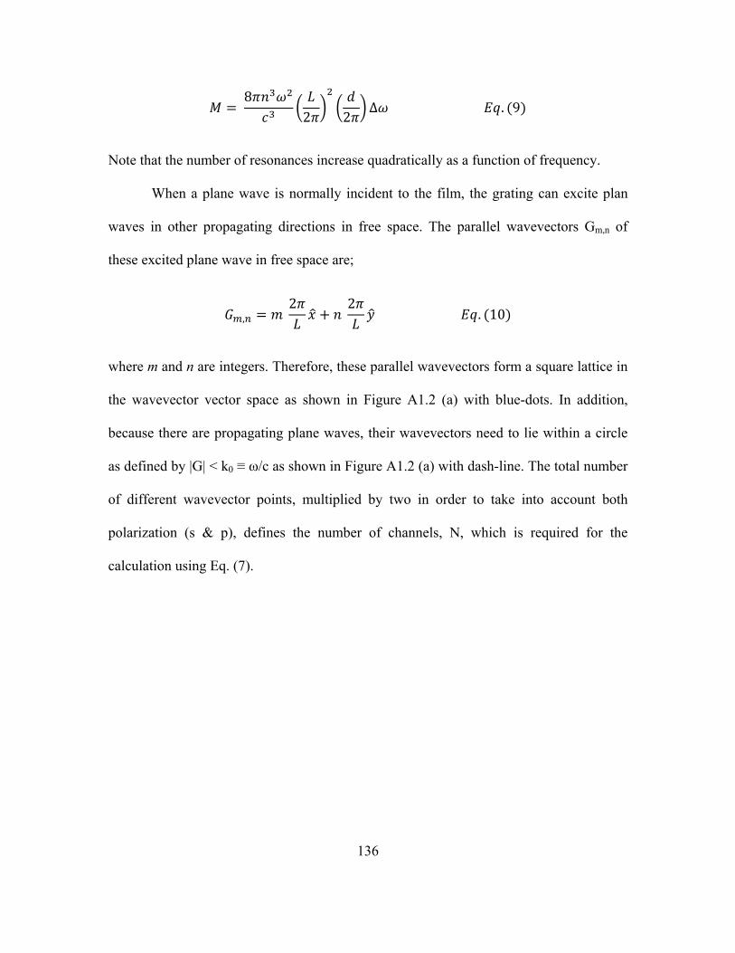
136
8
2 2∆ . 9
Note that the number of resonances increase quadratically as a function of frequency.
When a plane wave is normally incident to the film, the grating can excite plan
waves in other propagating directions in free space. The parallel wavevectors Gm,n of
these excited plane wave in free space are;
, 2
2
. 10
where m and n are integers. Therefore, these parallel wavevectors form a square lattice in
the wavevector vector space as shown in Figure A1.2 (a) with blue-dots. In addition,
because there are propagating plane waves, their wavevectors need to lie within a circle
as defined by |G| < k0 ≡ ω/c as shown in Figure A1.2 (a) with dash-line. The total number
of different wavevector points, multiplied by two in order to take into account both
polarization (s & p), defines the number of channels, N, which is required for the
calculation using Eq. (7).

137
Figure A2. (a) Channels in 2-D k-space for a grating with the square lattice periodic structure and (b) its upper limit of absorption enhancement. Reprinted from Reference [102]
When normalized frequency s = L/λ < 1, only two channels (N = 2) are existed after
accounting two polarizations in the normal direction, while the number of resonances
increases with frequency, ω, quadratically. In a result, the enhancement factor, F,
increases quadratically with frequency and reaches its maximum value, 4πn2, at s = 1 as
shown in Figure A1.2 (b). However, immediately above s = 1, the wavelength becomes
shorter than the period, L, and the number of channels increases to N = 10, leading to a
step-function drop of the enhancement factor, F, and in the regime of L >> λ, the
theoretical limit falls to 3-D bulk limit of 4n2.

138
A.4. Effect of Periodic Lattice Structure
In this section, we briefly talk about the effect of periodic lattice structure on the
enhancement factor, F. In reality, hexagonal (or tri-angluar) lattice is often found in self-
assembled nanoparticle in close-packing density which is also shown in this thesis. For
hexagonal lattice with period, L, the channels forms a hexagonal lattice in k-space as
shown in Figure A1.3 (b). The distance between the nearest two channels at k-space is;
2
√3
2
which is shown in Figure A1.3 (a) and this is larger than that of the square lattice, 2π/L
(Figure A1.2 (a)). As a result, for normally incident light, the frequency range where the
grating operates with only 2 channels is larger,
0 2
√3,
compared to the case of the square lattice (0 < s <1). This leads to a higher maximum
enhancement factor of;
8√3
as shown in Figure A1.3 (b). However, like square lattice, the enhancement factor is also
drop to bulk limit, 4n2, when the period becomes larger, L >> λ.

139
Figure A3. (a) Channels in 2-D k-space for a grating with hexagonal lattice periodic structure and (b) its upper limit of absorption enhancement. Reprinted from Reference [102]