development of tcad modeling for low field electronics
TRANSCRIPT

HAL Id: tel-01286315https://tel.archives-ouvertes.fr/tel-01286315
Submitted on 10 Mar 2016
HAL is a multi-disciplinary open accessarchive for the deposit and dissemination of sci-entific research documents, whether they are pub-lished or not. The documents may come fromteaching and research institutions in France orabroad, or from public or private research centers.
L’archive ouverte pluridisciplinaire HAL, estdestinée au dépôt et à la diffusion de documentsscientifiques de niveau recherche, publiés ou non,émanant des établissements d’enseignement et derecherche français ou étrangers, des laboratoirespublics ou privés.
Development of TCAD modeling for low field electronicstransport and strain engineering in advanced Fully
Depleted Silicon On Insulator (FDSOI) CMOStransistors
Olivier Nier
To cite this version:Olivier Nier. Development of TCAD modeling for low field electronics transport and strain engineeringin advanced Fully Depleted Silicon On Insulator (FDSOI) CMOS transistors. Micro and nanotech-nologies/Microelectronics. Université Grenoble Alpes; Università degli studi (Udine, Italie), 2015.English. �NNT : 2015GREAT141�. �tel-01286315�

THÈSE Pour obtenir le grade de
DOCTEUR DE LA COMMUNAUTÉ UNIVERSITÉ GRENOBLE ALPES
préparée dans le cadre d’une cotutelle entre l’université
Grenoble Alpes et l’université d’Udine. Spécialité : Nano électronique et Nano Technologies
Arrêté ministériel : le 6 janvier 2005 - 7 août 2006
Présentée par
Olivier Nier Thèse dirigée par Raphaël Clerc
codirigée par Denis Rideau, David Esseni et Jean-Charles Barbé
préparée au sein des Laboratoires IMEP-LAHC, le CEA-Leti, de l’entreprise STMicroelectronics et de l’université d’Udine
dans l’École Doctorale « Electronique, Electrotechnique, Automatique et traitement du signal »
Development of TCAD modeling for low field electronics transport and strain engineering in advanced Fully Depleted Silicon On Insulator
(FDSOI) CMOS transistors
Thèse soutenue publiquement le « 18 Décembre 2015 », devant le jury composé de :
Mr. Ghibaudo Gerard CNRS, IMEP LAHC Président Mr. Jungemann Christophe Aachen University Rapporteur
Mr. Delerue Christophe CNRS, IEMN Rapporteur
Mr. Rideau Denis STMicroelectronics Co-encadrant
Mr. Barbé Jean-Charles CEA LETI Co-encadrant
Mr. Esseni David Université d’Udine Co-directeur de thèse
Mr. Clerc Raphael Université Jean Monnet Directeur de thèse

2
3
Abstract
The design of nanoscale CMOS devices brings new challenges to TCAD community. Indeed,
nowadays, CMOS performances improvements are not simply due to device scaling but also to the
introduction of new technology “boosters” such as new transistors architectures (FDSOI, trigate),
high-k dielectric gate stacks, stress engineering or new channel material (Ge, III-V). To face all these
new technological challenges, Technology Computer Aided Design (TCAD) is a powerful tool to
guide the development of advanced technologies but also to reduce development time and cost. In this
context, this PhD work aimed at improving the modeling for 28/14 and 10FDSOI technologies, with a
particular attention on mechanical strain impacts. In the first section, a summary of the main models
implemented in state of the art device simulators is performed. The limitations and assumptions of
these models are highlighted and developments of the in-house STMicroelectronics KG solvers are
discussed. In the second section, a “top down” approach has been set-up. It has consisted in using
advanced physical-based solvers as a reference for TCAD empirical models calibration. Calibrated
TCAD reproduced accurately split-CV mobility measurements varying the temperature, the back bias
and the Interfacial Layer (IL) thickness. The third section deals with a description of the
methodologies used during this thesis to model stress induced by the process flow. Simulations are
compared to nanobeam diffraction (NBD) strain measurements. The use and calibration of available
TCAD models to efficiently model the impact of stress on mobility in a large range of stress (up to
2GPa) is also discussed in this section. The last part deals with TCAD modeling of advanced CMOS
devices for 28/14 and 10FDSOI technology development. Mechanical simulations are performed to
model the stress profile in transistors and several solutions to optimize the stress configuration in sSOI
and SiGe-based devices have been presented.

4
Contents: Introduction
Chapter I: Device modeling: physics and state of the art models
description for advanced transport solvers
I.1 Introduction .................................................................................................................................... 20
I.2 Band structures calculation ........................................................................................................... 21
1.2.1 The k.p method .......................................................................................................................... 21
1.2.2 The effective mass approximation for the conduction bands .................................................... 22
1.2.3 The 6-bands k.p model for the valence bands ........................................................................... 24
1.2.4 Parameters for SiGe channel ..................................................................................................... 26
I.3 Transport models ............................................................................................................................ 27
I.3.1 Semiclassical models ................................................................................................................. 27
I.3.2 Quantum model .......................................................................................................................... 31
I.4 Physics-based modeling of scattering mechanisms ..................................................................... 33
I.4.1 Scattering in a 2D electron gas .................................................................................................. 33
I.4.2 Phonons scattering ..................................................................................................................... 34
I.4.3 Surface roughness scattering ...................................................................................................... 35
I.4.4 Coulomb scattering .................................................................................................................... 38
I.4.5 Alloy scattering .......................................................................................................................... 41
I.4.6 Screening: ................................................................................................................................... 42
I.5 Conclusion: ...................................................................................................................................... 43
Chapter II: Physics-based modeling of low field transport in FDSOI
transistors and comparison with experiments II.1 Introduction ................................................................................................................................... 45
II.2 Advanced transport solvers comparison: Monte Carlo and Kubo Greenwood approaches
compared to NEGF simulations. ......................................................................................................... 45
II.2.1 Solvers description .................................................................................................................... 46
II.2.2 Methodology of comparison of different approaches ............................................................... 46
II.2.3 Advanced solvers comparison .................................................................................................. 49
II.3 Split-CV mobility measurements in FDSOI structures: experimental results and calibration.
................................................................................................................................................................ 54
II.3.1 Sample processed ...................................................................................................................... 54
II.3.2 Impact of the back bias ............................................................................................................. 55
II.3.3 Impact of the interfacial layer thickness ................................................................................... 57

5
II.3.4 Impact of the Temperature ........................................................................................................ 59
II.3.5 Universal behavior of the mobility: extraction of the parameter η in FDSOI devices ............. 59
II.4 Calibration for empirical solvers and comparison to measurements ...................................... 62
II.4.1 Process simulation in TCAD .................................................................................................... 62
II.4.2 TCAD empirical mobility model calibration ............................................................................ 62
II.4.3 Comparison to Experimental data............................................................................................. 65
II.5 Conclusion ..................................................................................................................................... 67
Chapter III: Mechanical simulations of the process-induced stress in
14FDSOI MOSFETs and comparison with nanobeam diffraction strain
measurements
III.1 Introduction ................................................................................................................................. 70
III.2. Methodology for mechanical stress modeling .......................................................................... 70
III.2.1 Generality about stress and strain tensors ............................................................................... 71
III.2.3 Boundary conditions ................................................................................................................ 73
III.2.4 Material properties for mechanical stress simulations ............................................................ 75
III.2.5 Process-induced stress ............................................................................................................. 79
III.3 Strain measurement techniques ................................................................................................. 82
III.4 TCAD Stress-dependent mobility models. ................................................................................ 83
III.5 Conclusion .................................................................................................................................... 91
Chapter IV: ST-oriented device applications
IV.1 Introduction ................................................................................................................................. 93
IV.2. Process flow description for 14FDSOI technology .................................................................. 93
IV.3 28FDSOI/14FDSOI mechanical stress study ............................................................................ 94
IV.3.1 STI process steps and layout effects. ...................................................................................... 94
IV.3.2 Stress relaxation during STI process steps: NBD Strain measurements. ................................ 97
IV.3.3 TCAD calibration on NBD measurements.............................................................................. 99
IV.4.3 SiGe Source and Drain .......................................................................................................... 104
IV.4 Stress state optimization for 14FDSOI devices. ...................................................................... 107
IV.4.1 Introduction of a piezoelectric layer ..................................................................................... 107
IV.4.2 Stress configuration optimization for n- and p-type MOSFETs. .......................................... 108
IV.5 Conclusion .................................................................................................................................. 113

6
Acknowledgments
First of all, I would like to acknowledge my advisors Raphael Clerc, Denis Rideau, David Esseni and
Jean-Charles Barbé for their guidance and support throughout the PhD. I thank them for their deep
knowledge in the physics of carrier transport in semiconductors but also for being a constant source of
motivation and inspiration. I am also grateful for their availabilities, encouragements and their help for
writing this manuscript.
This PhD work held at Grenoble (STMicroelectronics Crolles, IMEP LAHC and CEA LETI) and in
Udine. I thank Clément Tavernier for his welcome and support within STMicroeletronics Crolles
TCAD team. I thank Luca Selmi, David Esseni and Pierpaolo Palestri for the year spent in Udine. It
was a fruitful trip for my PhD work but also a wonderful life experience. Thank you for having
allowed me to live this experience.
I would like to thank all my colleagues and friends from STMicroelectronics Crolles and university of
Udine for their help and the great moments spent together during these three years. From Crolles and
Grenoble area, I would like to thank Olivier, Zahi, Floria, Sebastien, Fabio, Quentin, Assawer, Yvan,
Gabriel, Fred, Marie-Anne, Vincent Komi, Sylvain and Guillaume. From Udine, I would like to thank
Federico, Daniel, Patrik, Francesco, Alberto and Stefano.
Finally, I would like to acknowledge Olivier Noblanc and Clement Tavernier for their confidence and
for giving me the opportunity to work again for STMicroelectronics. A new adventure begins by
working on CMOS imagers.

7
Publications and conferences Nier, O., Rideau, D., Niquet, Y. M., Monsieur, F., Nguyen, V. H., Triozon, F., Cros, A., Clerc, R.,
Barbé, JC., Palestri, P., Esseni, D., Duchemin, I., Smith,L. , Silvestri, L., Nallet, F., Tavernier, C.,
Jaouen, H., Selmi, L. (2013). Multi-scale strategy for high-k/metal-gate UTBB-FDSOI devices
modeling with emphasis on back bias impact on mobility. Journal of Computational Electronics,
12(4), 675-684.
Nier, O., Rideau, D., Clerc, R., Barbe, J. C., Silvestri, L., Nallet, F., Tavernier, C., Jaouen, H.
(2013, March). Limits and improvements of TCAD piezoresistive models in FDSOI transistors. In
Ultimate Integration on Silicon (ULIS), 2013 14th International Conference on (pp. 61-64). IEEE.
Nier, O., Rideau, D., Cros, A., Monsieur, F., Ghibaudo, G., Clerc, R., Barbé, JC., Tavernier, C.,
Jaouen, H. (2014, March). Effective field and universal mobility in high-k metal gate UTBB-
FDSOI devices. In Microelectronic Test Structures (ICMTS), 2014 International Conference on
(pp. 8-13). IEEE.
Nier, O., Esseni, D., Rideau, D., Palestri, P., Selmi, L., Cros, A., Clerc, R., Barbé, JC., Tavernier,
C., Jaouen, H. “Experimental and physics-based modeling of transport in thin body, strained
Silicon-On-Insulator transistors for ultra-low power CMOS technologies” Gruppo Elettronica 2014.
Andrieu, F., Casse, M., Baylac, E., Perreau, P., Nier, O., Rideau, D., Berthelon, R., Pourchon, F.,
Pofelski, A., De Salvo, B., Gallon, C., Mazzocchi,, V., Barge, D., Gaumer, C., Gourhant, O.,
Cros, A., Barral, V., Ranica, R., Planes, N., Schwarzenbach, W., Richard, E., Josse, E., Weber, O.,
Arnaud, F., Vinet, M., Faynot, O., Haond, M. (2014, September). Strain and layout management in
dual channel (sSOI substrate, SiGe channel) planar FDSOI MOSFETs. In Solid State Device
Research Conference (ESSDERC), 2014 44th European (pp. 106-109). IEEE.
Rideau, D., Niquet, Y. M., Nier, O., Cros, A., Manceau, J. P., Palestri, P., Esseni, D., Nguyen, V.
H., Triozon, F., Barbé, JC., Duchemin, I., Garetto, D., Smith,L. , Silvestri, L., Nallet, F., Clerc, R.,
Weber, O., Andrieu, F., Josse, E., Tavernier, C., Jaouen, H. Mobility in High-K Metal Gate
UTBB-FDSOI Devices: from NEGF to TCAD perspectives. Electron Devices Meeting (IEDM),
2013 IEEE International (pp. 12.5.1 - 12.5.4)
Rideau, D., Monsieur, F. ; Nier, O. ; Niquet, Y.M. ; Lacord, J. ; Quenette, V. ; Mugny, G. ; Hiblot,
G. ; Gouget, G. ; Quoirin, M. ; Silvestri, L. ; Nallet, F. ; Tavernier, C. ; Jaouen, H.. (2014,
September). Experimental and theoretical investigation of the ‘apparent’mobility degradation in Bulk and UTBB-FDSOI devices: A focus on the near-spacer-region resistance. In Simulation of
Semiconductor Processes and Devices (SISPAD), 2014 International Conference on (pp. 101-104).
IEEE.
Rideau, D., Niquet, Y. M., Nier, O., Palestri, P., Esseni, D., Nguyen, V. H., Triozon, F.,
Duchemin, I., Garetto, D., Smith,L. , Silvestri, L., Nallet, F., Tavernier, C., Jaouen (2012).
Mobility in FDSOI devices: Monte Carlo and Kubo Greenwood approaches compared to NEGF
simulations. Abstract, International workshop on computational electronics (IWCE), 2013.
Niquet, Y. M., Nguyen, V. H., Triozon, F., Duchemin, I., Nier, O., Rideau, D. (2014). Quantum
calculations of the carrier mobility: Methodology, Matthiessen's rule, and comparison with semi-
classical approaches. Journal of Applied Physics, 115(5), 054512.

8
Nguyen, V. H., Niquet, Y. M., Triozon, F., Duchemin, I., Nier, O., Rideau, D. (2014). Quantum
Modeling of the Carrier Mobility in FDSOI Devices. Electron Devices, IEEE Transactions on
(Volume: 61, Issue: 9 ). pp. 3096 - 3102
Pereira, F. G., Rideau, D., Nier, O., Tavernier, C., Triozon, F., Garetto, D., ... & Pala, M. (2015,
January). Modeling study of the mobility in FDSOI devices with a focus on near-spacer-region. In
Ultimate Integration on Silicon (EUROSOI-ULIS), 2015 Joint International EUROSOI Workshop
and International Conference on (pp. 49-52). IEEE.
Tavernier, C., Pereira, F. G., Nier, O., Rideau, D., Monsieur, F., Torrente, G., ... & Barbe, J. C.
(2015, September). TCAD modeling challenges for 14nm FullyDepleted SOI technology
performance assessment. In Simulation of Semiconductor Processes and Devices (SISPAD), 2015
International Conference on (pp. 4-7). IEEE.

9
List of figures
Figure 1 : Evolution of the gate stack dimension with the technology node at HP. Data are extracted from
IEDM/VLSI presentations. .................................................................................................................... 16
Figure 2 : STMicroelectronics and Intel roadmaps. ................................................................................. 17
Figure 3 : List of available solvers used during this thesis to model transport in FDSOI devices................... 18
Figure 4 : Description of the internal and external collaborations during the thesis. ................................... 19
Figure 5 : Valence band parameters for Si1-xGex alloy used in literature. Full lines are extracted from [14],
dotted lines from [13] and symbols from [12] (linear interpolation). .................................................................. 27
Figure 6 : Flowchart of a typical Monte Carlo program. .................................................................................... 30
Figure 7 : Overall flowchart of the MSMC solver ............................................................................................... 30
Figure 8 : Carrier density with NEGF in a 4 nm thick FDSOI film. Interface roughness generated with an
exponential autocorrelation function (Δ=0.47 nm and Λ=1.3 nm). ..................................................................... 32
Figure 9 : NEGF resistance of the FDSOI film as a function of length. The slope gives the mobility, while the
intercept at L=0 is the quantum “ballistic” resistance. ....................................................................................... 32
Figure 10 : Cross-section of a FDSOI MOSFET illustrating scattering mechanisms responsible of the mobility
degradation: 1) is scattering with phonons, 2) and 3) are surface roughness scattering at the front and back
interface, 4) is remote Coulomb scattering due to the presence of charge in the gate stack and 5) is remote
surface roughness scattering. ............................................................................................................................... 33
Figure 11 : Silicon intervalley phonons type: g-type phonon goes in the opposite Δ valley with the same orientation; f-type phonon that scatters from one Δ valley to one of the four Δ valleys with different orientation. .............................................................................................................................................................................. 34
Figure 12 : Schematic of the Surface roughness at the semiconductor-oxide interface. ................................ 35
Figure 13 : Schematic of the different density of carriers affecting mobility through Local Coulomb or remote
Coulomb scattering. The coordinate system (axe z) is also shown on this figure. ......................................... 38
Figure 14 : Unscreened Coulomb scattering potential of a point charge a) located at 0.5 nm from the Hf02/SiO2
interface calculated for different high-k permittivities b) located at different positions 権ど inside the high-k
dielectric. q=2×10⁸ m-1. ....................................................................................................................... 40
Figure 15 : Unscreened Coulomb scattering potential calculated using two different boundary conditions: 1/ by
considering the thickness of the high-k as infinite (full lines) 2/ by fixing G=0 at high-k/metal interface (dashed
line). The charge is located in the high-k a) or in the channel b). FDSOI device. TSI=7.5 nm. SiO2 BOX of 25 nm
(ε=3.9). The metal gate stack consists in a 1.8 nm thick high-k material (ε=20) on top of a 1.0 nm thick SiO2 layer (ε=3.9). ...................................................................................................................................... 40
Figure 16 : Remote Coulomb-limited mobility as a function of the inversion density for various high-k
thicknesses. Nit=1×1013 cm-2. TSI=7.5 nm. SiO2 box of 25 nm (ε=3.9). The metal gate stack consists in a high-k
material with varying thicknesses (ε=20) on top of a 1.0 nm thick SiON layer (ε=5.2). ................................ 40
Figure 17 : Unscreened Coulomb scattering potential as a function of the position z for charges located at z0.
Boundary condition: G=0 at high-k/metal interface. Structure of Figure 16................................................ 41
Figure 18 : a) Hole effective mobility as a function of the effective field for SGOI and sSGOI with varying
channel germanium mole fraction. ......................................................................................................... 42
Figure 19 : Δ=0.47 nm, Λ=1.3 nm, autocorrelation: exponential. Doping concentration=1×1018 cm-3. Structure
of Figure 15. ....................................................................................................................................... 43
Figure 20 : Error E produced by the extraction of mobility components (surface roughness and remote
coulomb scattering) using the Matthiessen’s rule. ................................................................................... 47
Figure 21 : (a) Total KG mobility μ�o�KG = μPH + SR + RCSKG (nRCS = ぬ.ど × などなぬc� − に) compared
with Matthiessen’s rule μ�o�M from eq. 2.1 and μ�o�M, eff from eq. 2.2. (b) Error induced by the Matthiessen
rule μ�o�M, effon the total mobility. ....................................................................................................... 48

10
Figure 22 : n- (left) and p- (right) FDSOI experimental electric field (equation 2.7) assuming η = 0.5 compared to the simulated theoretical average field (equation 2.6). VB from -10 V to 10 V in steps of 2V. IL EOT =1.8
nm; T=300 K. ..................................................................................................................................... 49
Figure 23 : Schematic of the simulated FDSOI devices. The comparison is done for surface roughness, phonons
and remote Coulomb scattering ............................................................................................................. 50
Figure 24 : Comparison of phonon-limited electrons mobility in FDSOI devices as a function of active layer
thickness. ............................................................................................................................................ 50
Figure 25 : Surface roughness-limited electrons mobility a) as a function of the effective field for TSi=2.6 nm,
4.0 nm and 7.0nm. b) as a function of TSi extracted at Eeff= 0.08 and 0.77 MV/cm. (exponential SR
autocorrelation with Δ=0.47 nm; Λ=1.3 nm). ......................................................................................... 51
Figure 26 : SR-limited mobility as a function of the inversion charge calculated using Sband and UTOXPP for
different channel doping concentrations at VB=0V (a) and VB=8V (b). (Exponential auto-correlation with
∆=0.47 nm and Λ=1.3 nm). .................................................................................................................. 52
Figure 27 : SR-limited mobility as a function of Eeff calculated for different channel doping concentration at
VB=0 and 8V. ..................................................................................................................................... 52
Figure 28 : Remote-Coulomb-limited electron mobility as a function of the inversion charge for devices with
two different IL EOT: 1.0 nm and 4.0 nm. Nit = 5×1013 cm-2 .................................................................... 52
Figure 29 : Local-Coulomb-limited electron mobility as a function of a) the effective field and b) the inversion
charge for various channel doping concentrations and for VB=0V and 8V. The metal gate stack consists in a
1.8 nm thick high-k material (ε=20) on top of a 1.2 nm thick SiON layer (ε=6.6). ........................................ 53
Figure 30 : Comparison of phonon-limited holes mobility in FDSOI devices as a function of the inversion
charge for three different silicon thicknesses (3.0, 5.0 and 7.5 nm). ........................................................... 53
Figure 31 : Surface roughness-limited holes mobility as a function of the inversion charge for TSi=3.0 nm, 5.0
nm and 7.5 nm..................................................................................................................................... 54
Figure 32 : a) Front-end process flow for 28FDSOI technology. b) Cross-section of a FDSOI MOSFET ....... 55
Figure 33 : Gate capacitance as a function of the gate voltage for various back biases ranging from -10V to
10V per steps of 2V in n- (a) and p-MOS (b) devices. Tinv=2.65 nm; TSi=7.5 nm; T=300 K. TCAD calibration
shown for VB=-8, 0 and 8V. ................................................................................................................. 55
Figure 34 : Threshold voltage variation (reference at VB=0 V) as a function of the back bias in n- and pMOS
devices. Tinv=2.65 nm; TSi=7.5 nm; T=300 K. ......................................................................................... 56
Figure 35 : Experimental effective mobility as a function of the inversion charge for various back biases
ranging from -10V to 10V in steps of 2V, in n- (a) and pMOS devices (b). Tinv=2.65 nm; TSi=7.5 nm; T=300 K.
......................................................................................................................................................... 56
Figure 36 : Effective experimental mobility as a function of the back bias for various inversion densities:
Ninv=1×10¹³, 5×10¹² and 2×1012 cm-². IL EOT= 1.8 nm; TSi=7.5 nm; T=300K. Symbols represent biases
conditions whose density profiles are extracted in Figure 37: 1/ VB= -5 V, VG=2.0 V; 2) VB=0 V, VG=1.6 V; 3)
VB=5 V, VG=1.2 V. ............................................................................................................................. 57
Figure 37 : Simulated profile of the potential (a) and the electron density (b) in the channel for various biases
conditions using PS simulations): 1/ VB=-5 V, VG=2.0 V; 2) VB=0 V, VG=1.6 V; 3) VB=5 V, VG=1.2 V.
nMOS device, IL EOT= 1.8 nm. TSi=7.5 nm; T=300 K. ............................................................................ 57
Figure 38 : Gate capacitance as a function of the gate voltage for devices with different IL EOT varying from
0.7 nm to 3.0 nm. ................................................................................................................................. 58
Figure 39 : n- (a) and pMOS (b) experimental effective mobility as a function of the inversion charge for
structures with various IL physical thicknesses (VB=0 V). ........................................................................ 58
Figure 40 : Effective experimental mobility as a function of the inversion charge for various VB ranging from -
10 V to 10 V in steps of 2 V. nFDSOI device : IL EOT= 1.8 nm. T=233, 300 and 450 K. .............................. 59
Figure 41 : Effective experimental mobility as a function of the inversion charge for various VB ranging from -
10 V to 10 V in steps of 2 V. pFDSOI device : IL EOT= 1.8 nm. T=233, 300 and 450 K. .............................. 59

11
Figure 42 : Extracted value of parameter η using Eq. 2.8 in n- and pFDSOI devices for various temperatures
(T=233, 300 and 450 K). nFDSOI device: IL EOT = 1.8 nm. The domain of validity corresponds to the strong
front inversion regime. VB=0 V. ............................................................................................................ 60
Figure 43 : n- (left) and p- (right) FDSOI experimental effective mobility as a function of the effective field. VB
ranging from -10 V to 10 V in steps of 2 V. Effective field calculated using Eq. 2.7 (η=0.42 for nFDSOI and
η=0.36 for pFDSOI). IL EOT = 1.8 nm. T=300 K. .................................................................................. 60
Figure 44 : Extracted value of parameter η using Eq. 2.8 in a nFDSOI device for various VB ranging from -10
V to 10 V. IL EOT = 1.8 nm. T=300 K. In the front inversion regime (VB<0), η=0.42 while in the forward regime (VB>0), η varies significantly with VB......................................................................................... 61
Figure 45 : n- and p- FDSOI experimental effective mobility as a function of the effective field sweeping the
back terminal or the gate terminal. Eq.2.7 has been used for the evaluation of the effective field with η=0.42 for nFDSOI and η=0.36 for pFDSOI devices. IL EOT = 1.8 nm. T=300 K. ..................................................... 61
Figure 46 : n- (left) and p- (right) FDSOI experimental effective mobility as a function of the effective field. VB
ranging from -10 V to 10 V in steps of 2 V. Effective field calculated using Eq. 2.7 (η=0.62 for nFDSOI and η=0.5 for pFDSOI). IL EOT = 1.8 nm. T=300 K. .................................................................................... 62
Figure 47 : TEM cross-section superimposed to a process simulation of a UTBB-FDSOI device. ................. 62
Figure 48 : PH + LC and LC-limited mobility determined using Philips unified mobility model. .................. 64
Figure 49 : nMOS effective remote Coulomb-limited electron mobility in FDSOI devices as a function of the
inversion charge. KG and TCAD simulations are performed a) for various high-k/IL interface charge density in
a device with IL EOT=1.8 nm and b) for various IL EOT for a fixed interface charge density C=5× などなぬ cm-2.
Tsi=7.5 nm; T=300 K. TCAD model parameters: μな = ねひぬ cm²/V/s, 潔建堅欠券嫌 = な × などなぱ cm-3,荒 = な.ね, �に =な, 健潔堅件建 = な.にの × など − ば 潔兼. Phonons parameters of Table 7. ................................................................ 65
Figure 50 : Same as Figure 49 but for holes. TCAD models parameters: μな = ねのね cm²/V/s, 潔建堅欠券嫌 = な ×などなぱ cm-3, 荒 = な.は, �に = な, 健潔堅件建 = な.の × など − ば 潔兼. .......................................................................... 65
Figure 51 : n-MOS mobility as a function of the inversion charge a) for structures with various IL EOT or b) at
different temperatures. Comparison between TCAD, KG solvers and experiments. ...................................... 66
Figure 52 : p-MOS mobility as a function of the inversion charge for structures with various IL EOT a) or at
different temperatures b) Comparison between TCAD, KG solvers and experiments. ................................... 66
Figure 53 : n- and pMOS mobility extracted at fixed inversion density as a function of a) the IL EOT b) the
Temperature. Comparison between TCAD, KG solvers and experiments. ................................................... 67
Figure 54 : Simulated effective mobility as a function of the back bias for various inversion densities: Ninv=1×など13 and 2× など12 cm-². Tinv=2.65 nm; TSi=7.5 nm; T=300 K. .................................................................... 67
Figure 55 : Classification of stress techniques. ....................................................................................... 70
Figure 56 : Definition of the stress tensor components. The first subscript refers to the direction normal to the
face on which the stress is applied. The second subscript corresponds to the direction of the stress. .............. 71
Figure 57 : Main boundary conditions (BC) in 2D. Left) “Free” BC that implies a zero normal stress on each side. Right) Dirichlet BC applied on each side of the simulation domain. (1) corresponds to a fixed point and
(2) restricts the displacement to one direction. ........................................................................................ 73
Figure 58 : Evolution of the stress with the width dimension. This stress value corresponds to the mean stress in
the channel after the STI process steps. .................................................................................................. 74
Figure 59 : 3D TCAD simulations of FDSOI devices with varying dimensions after STI process steps. .......... 74
Figure 60 : a) 3D TCAD simulations of the longitudinal stress in the device. The dashed lines represent the
different 2D cuts of the structure. (b) 2D cut of the device. The dashed line represents the 1D cut of the
structure along the channel. .................................................................................................................. 75
Figure 61 : Simulation of the (a) transversal and (b) longitudinal stress profile in the channel. Profile of Figure
60. ..................................................................................................................................................... 75
Figure 62 : Schematic of the uniaxial linear elasticity. ............................................................................ 76
Figure 63 : Schematic of the viscoelastic material behavior corresponding to the Maxwell model. ............... 77

12
Figure 64 : Silicon oxide and nitride viscosity as a function of 1000/T. Comparison between the values used in
our simulations and measurements from literature ([Senez-96]: [137] and [Carlotti-02]: [138] ). ................ 78
Figure 65 : Schematic of the stress/strain relation to illustrate the plastic regime. Extracted from [141]. ...... 78
Figure 66 : Value of the yield stress for Si1-xGex as a function of the Germanium concentration. [Hartmann –
2011]: [107], [People and Bean – 1985]: [108]. ..................................................................................... 78
Figure 67 : (a) Schematic diagram of relaxed SiGe and silicon films. (b) Schematic diagram showing the lattice
distortion when the SiGe film is growth on top of the silicon film: the SiGe film is compressively strained.
Figure extracted from [140]. ................................................................................................................ 80
Figure 68 : TEM cross-section of the device after the formation of the SiGe channel by condensation. TEM
study performed by the team “physical characterization”. ........................................................................ 81
Figure 69 : Electron Dispersive X-Ray (EDX) Spectroscopy analysis along the profile shown in Figure 68.
EDX analysis performed by the team “physical characterization”. ............................................................ 81
Figure 70 : Relative strain versus profile (shown in Figure 68) measured by NBD. NBD study performed by the
team “physical characterization”. ......................................................................................................... 81
Figure 71 : TCAD simulation of the deposition of the STI (540°C) on a full wafer. ...................................... 82
Figure 72 : nMOSFET piezo coefficients calculated using a KG solver and compared to literature. 欠岻 �なな,�なに, 欠券穴 �なぬ are obtained by applying a longitudinal, transversal and vertical stress on a <100> -
oriented channel MOSFET. 欠岻 �詣 欠券穴 �劇 are obtained by applying a longitudinal and transversal stress on
<110>-oriented channel MOSFET. Smith54: [123], Thompson06: [132], Weber07: [106]. ......................... 85
Figure 73 : Same as Figure 72 but for pMOSFETs. PI1. Canali79: [125]. ................................................. 85
Figure 74 : Picture (a) and schematic diagram (b) of the 4 points the bender used for piezoresistive coefficients
measurements ..................................................................................................................................... 86
Figure 75 : Mobility variation with stress for a) <100>-oriented and b) <110>-oriented channel nFDSOI
devices. The extracted piezoresistance coefficients are listed in Table 16. Measurements are performed on
28FDSOI technology (device described in part II.3). ............................................................................... 87
Figure 76 : Mobility variation with stress for <110>-oriented channel pFDSOI devices. The extracted
piezoresistance coefficients are listed in Table 16. ................................................................................... 87
Figure 77 : Hole mobility variation (extracted at Eeff=1 MV/cm) in <110>-oriented silicon channel pMOSFETs
as a function of the longitudinal uniaxial stress (stress applied in the <110> direction). Linear model: �航/航 =−�詣 × �. Exponential model: �航/航 = 結捲喧 岫−�詣 × �岻 with �詣 = ばば × など − なな 鶏欠 − な ....................... 88
Figure 78 : Hole mobility variation (extracted at Eeff=1MV/cm) in <100> (a) and <110> (b) silicon channel
pMOSFETs as a function of stress for three different uniaxial stress direction and three biaxial stress types.
Symbols are MCmob results and lines are UTOXPP results. ..................................................................... 90
Figure 79 : Electron mobility variation (extracted at Eeff=1 MV/cm) in <100> (a) and <110> (b) silicon
channel nMOSFETs as a function of stress for three different uniaxial stress direction and three biaxial stress
types. Symbols are MCmob results and lines are UTOXPP results. ............................................................ 90
Figure 80 : Simplified description of the process flow for 14FDSOI technology. ......................................... 93
Figure 81 : TCAD process simulation of 14FDSOI technology after a) STI isolation steps, b) Gate stack
deposition, c) spacer formation and d) SiGe S&D epitaxy......................................................................... 94
Figure 82 : STI process flow for 28/14 FDSOI technology. ...................................................................... 95
Figure 83 : Schematic description of the STI process steps. It can be noticed that a dual STI (deep and shallow
STI) has been analyzed. ........................................................................................................................ 95
Figure 84 : Evolution of the stress profile along the channel direction during STI process steps. Numbers in in
the figure corresponds to process steps described in Figure 83. ................................................................ 96
Figure 85 : Simulation of the evolution of the stress profile along the channel direction. Two cases have been
considerate: SiGe first and SiGe last. Lactive=130 nm. ............................................................................... 96
Figure 86 : Left) Simulated mean longitudinal stress (average on the channel region) with Lactive and the mean
transversal stress (average on the whole width) with Wactive. Right) Simulated hole mobility variation with Lactive
and Wactive using KG solver (channel wafer) ............................................................................................ 97

13
Figure 87 : Simulated (KG solver) hole mobility variation (extracted at Eeff=1 MV/cm) in a) <100> and b)
silicon channel pMOSFETs as a function of stress. ................................................................................... 97
Figure 88 : TEM picture of the studied device. Measurements are performed after STI formation steps. The
dotted line corresponds to the profile where NBD measurements have been performed. ............................... 98
Figure 89 : Measurements of the deformation profile (εxx and εyy) thanks to NBD measurements. Profile shown
in Figure 88. xGe = 22%. Measurements have been performed before STI anneal. ....................................... 98
Figure 90 : Measurements of the deformation profile εxx .......................................................................... 98
Figure 91 : Relative longitudinal deformation εxx measured by NBD, and comparison to TCAD simulations. . 99
Figure 92 : TEM pictures of the simulated structure. The dotted line corresponds to the profile where NBD
measurements have been performed. ...................................................................................................... 99
Figure 93 : Comparison between TCAD simulations and NBD measurements of the deformation profile εxx post
STI patterning and at the end of the process. Device of Figure 92. ............................................................ 100
Figure 94 : Left: Definition of the notation SA and SB. Right: comparison between measured relative Iodlin
variation (reference: long SA/SB) and TCAD simulations as a function of SA/SB ....................................... 101
Figure 95 : Comparison between measured relative Iodlin variation (reference: long SA/SB) and TCAD
simulations as a function of W. ............................................................................................................ 101
Figure 96 : a) variation of the current as a function of Lactive. b) variation of the inverse current with 1/Lactive 102
Figure 97 : a) variation of the extracted longitudinal stress (thanks to more realistic methods) as a function of
Lactive and comparison to TCAD simulations. b) variation of the current with active length using MCmob model.
........................................................................................................................................................ 103
Figure 98 : Evolution of the extracted longitudinal stress as a function of SA dimensions using the ‘realistic method’. TCAD simulations are added to the data from three different lots. .............................................. 103
Figure 99: a) variation of the current as a function of Lactive. Comparison between the direct approach (value
λI) and the ‘realistic method (value λα). Points are measurements. ............................................................ 104
Figure 100 : Simulation of the deposition of SiGe source and drain for pMOSFET a) before and b) after the
deposition of the Si0.7Ge0.3 S&D on top of the Si0.78Ge0.22 channel. Note that only the half of the structure is
simulated. Device described in section IV.2. .......................................................................................... 104
Figure 101 : Cut of the longitudinal stress profile in the channel. Devices of Figure 100. A uniaxial
compressive stress of 200 MPa is added to the initially stressed Si0.78Ge0.22 channel. ................................... 105
Figure 102 : Simulated structures for device performance optimization. a) no S&D, (b) facetted S&D, (c) semi-
facetted and (d) non facetted. .............................................................................................................. 105
Figure 103 : Cut of the longitudinal stress profile in the channel. a) no S&D -> 1, (b) facetted S&D ->2, (c)
semi-facetted -> 4 and (d) non facetted ->3. Devices of Figure 102. ......................................................... 105
Figure 104 : TCAD pictures of the simulated structures. a) with and b) without spacer recess. Structures:
LCH=20 nm, Lactive=130 nm, xGechannel=22%. .......................................................................................... 106
Figure 105 : 1D cut in the channel of the longitudinal stress with (1 nm and 2 nm) and without recess after
spacer formation step. ......................................................................................................................... 106
Figure 106 : a) TCAD pictures of the simulated structures. b) 1D cut in the channel of the longitudinal stress
with (1 nm and 2 nm) and without recess after SiGe S&D epitaxy. ............................................................ 107
Figure 107 : Integration of a piezoelectric layer in the device: studied structures and patents in the literature.
[Wong-10]: [142], [Lolivier-11]: [143] and [Kronholz-14]: [144]. .......................................................... 107
Figure 108 : TCAD simulation of a UTBB-FDSOI device. The layer in the BOX corresponds to the
piezoelectric material.......................................................................................................................... 107
Figure 109 : a) Evolution of the longitudinal σxx, transversal σyy and vertical σzz stress component in the
channel due to the introduction of a V-doped ZnO piezoelectric layer. b) corresponding mobility variation for
electron. ............................................................................................................................................ 108
Figure 110 : 3D schematic of the SOI transistor. This figure is extracted from the deposited patent [150].
Concerning p-type MOSFETs, the performance improvement consists in relaxing the transversal stress value
(W direction). ..................................................................................................................................... 109

14
Figure 111 : a) Plan view of a RX mask used to form isolation trenches 106 delimiting the width of the SOI
structure. a) Plan view of a RC mask used to form isolation trenches 104 (STI) delimiting the length of the
structure. This figure is extracted from the deposited patent [150]. ........................................................... 110
Figure 112 : Description of a) classical and b) proposed STI process steps. .............................................. 110
Figure 113 : Description of the proposed process flow to decrease the stress relaxation only in the length
direction only. .................................................................................................................................... 111
Figure 114 : Description of the proposed process flow to selectively implant trenches delimiting the width
direction to enhance the relaxation. ...................................................................................................... 112
Figure 115 : Cross section of the SOI transistor. This figure is extracted from the deposited patent [152]. The
step 414 corresponds to the implantation of Germanium atoms through trenches 412. Layer 112 is the
semiconductor, layer 110 the insulator and 404 and 406 correspond to hard mask layers. .......................... 112
List of Tables
Table 1 : Parameters used for the calculation of the conduction band structure with the effective mass
approximation. ...................................................................................................................................................... 22
Table 2 : Parameters for the conduction band structure calculation [47] .......................................................... 23
Table 3 : Values of the Luttinger parameters 紘な, 紘に欠券穴 紘ぬ used in our simulations for silicon and germanium
.............................................................................................................................................................................. 26
Table 4 : Comparison of SR spectrum parameters � and � measured by AFM or TEM with those used in the
simulation (GPN model) to fit experimental mobility values. ............................................................................... 37
Table 5 : Alloy scattering potential: data from literature and value used in our simulation for holes mobility. . 41
Table 6 : Summary of the devices used for mobility measurements. .................................................................... 41
Table 7 : Phonons model parameters used for silicon taken from [85]. .............................................................. 50
Table 8 : Phonons and surface roughness mobility model parameters for holes. ................................................ 53
Table 9 : Parameters for Philips unified mobility model for electrons and holes [100]. ..................................... 64
Table 10 : Simulation parameters for KG solver s. .............................................................................................. 66
Table 11 : Compliance and stiffness constants for silicon and germanium [129] ............................................... 76
Table 12 : Coefficients for the temperature dependent viscosity model for silicon dioxide and nitride. ............. 77
Table 13 : Values of thermal coefficients used in our simulations ....................................................................... 79
Table 14 : Comparison of TEM-based strain measurement techniques. .............................................................. 83
Table 15 : Piezoresistive coefficients values for bulk silicon and in the case of an inversion layer. ................... 86
Table 16 : Piezoresistance coefficients extracted from wafer bending measurements ........................................ 87
Table 17 : MCmob model description for uniaxial stress. ................................................................................... 89
Table 18 : MCmob cross terms correction coefficients ........................................................................................ 89
Table 19 : Calibrated MCmob parameters for holes ........................................................................................... 91
Table 20 : Calibrated MCmob parameters for electrons. .................................................................................... 91
Table 21 : Piezoelectric material properties of ZnO, AlN and GaN. ................................................................. 108
Table 22 : Calculated values of strain and stress in V-doped ZnO films for an electric field of 3.2×10⁷ V/m. 108
Table 23 : Description of the proposed STI process flow to optimize the stress configuration in MOSFETs ... 110

15
List of abbreviations:
BOX; Buried OXide
BTE: Boltzmann Transport Equation
CBED: Convergent-Beam Electron Diffraction
CTE: Coefficient of Thermal expansion
DD: Drift Diffusion
EMA: effective mass approximation
EOT: Equivalent Oxide Thickness
FDSOI: Fully depleted Silicon On Insulator
GPN: Generalized Prange Nee
HP: High Power
HREM: High-Resolution Electron Microscopy
HoloDark: dark-field electron holography
LP: Low Power
LSTP: Low Stand-by Power (LSTP)
IL: interfacial layer
KG: Kubo-Greenwood
LCS: Local Coulomb Scattering
MC: Monte Carlo
MSMC: Multi-Subband Monte Carlo
NEGF: Non-Equilibrium Green Function
NBD: Nano-Beam Diffraction
PS: Poisson Schrödinger
RCS: Remote Coulomb Scattering
RTA: Relaxation Time Approximation
SCE: Short Channel Effects
SOI: Silicon On Insulator
STI: Shallow Trench Isolation
SR: Surface Roughness
sSOI: strained Silicon On Insulator
TEM: Transmission Electron Microscopy
TCAD: Technology computer-aided design
TDF: Tensorial Dielectric function

16
Introduction
Metal Oxide Semiconductor Field-Effect Transistor (MOSFET) is the semiconductor industry key
elementary device, enabling the development of the impressive number of electronic applications. The
International Roadmap for Semiconductors (ITRS) [1], which is the guideline for the technology
improvements in MOSFET fabrication, aims at anticipating risk factors in the developments of the
microelectronic industry. The diversification of microelectronic application has led to a diversification
of the ITRS for High Power (HP), Low Power (LP) and Low Stand-by Power (LSTP) roadmap.
Nevertheless, regardless to the applications, the semiconductor industry has steadily scaled device
dimensions to improve performance and to reduce cost [2]. From 20 µm to 90 nm technology nodes,
performance improvements were essentially due to the scaling of transistors dimensions according to
scaling rules (as illustrated in Figure 1 for gate oxide stack). Nevertheless, conventional scaling of
MOSFET dimensions, according to ITRS requirements, faces physical and economical limits. Indeed,
the scaling rules which have allowed for more than 30 years the semiconductor industry to constantly
improve transistors performance while reducing their costs, faces increasing difficulties and
limitations. These challenges are the control of leakage currents (short channel effects (SCE),
tunneling current through the gate insulator …), the enhancement of transport properties within the channel, and the control of variability (due to process or doping fluctuations).
Figure 1 : Evolution of the gate stack dimension with the technology node at HP. Data are extracted from
IEDM/VLSI presentations.
Nowadays, the ITRS performance requirement has led to the introduction of technology “boosters”,
such as the use of new transistors architectures (FDSOI, trigate), high-k dielectric gate stacks, stress
engineering or new channel material (Ge, III-V). The diversity of technological solutions has induced
different strategies in the industrial development, as illustrated in Figure 2 for STMicroelectronics and
INTEL. From the 28 nm technology node, STMicroelectronics has started the development (from
2010 to 2015) of planar transistors on Silicon On Insulator (SOI) substrate. This architecture has many
advantages, such as a better electrostatic control of the channel, leading to a reduction of SCE [3]. In
addition, contrary to FinFET for instance, the dimensions of FDSOI planar transistors can be easily
changed on the same circuit, as sometimes required in non-digital function, such as analog, RF, or I/O
circuits. It also offers the possibility of adjusting the threshold voltage by applying a back bias (when
thin buried oxide BOX are used), giving flexibility to circuit designers to combine high performance
and low power transistors in the same technology. The use of lightly doped channel may also reduce
101
102
103
104
105
10-1
100
101
102
103
HP MOSFETs @ IDEM/ VLSI
Tecnology Node [nm]
EO
T/T
ox [
nm
]
1990: 1 m
2008: 32 nm2007: 45 nm
1975: 20 m
1985: 5 m
1980: 10 m
Strain
2005: 65 nm
2003: 90 nm
1995: 0.35 m2000: 0.18 m
2001: 0.13 m
HK/MG
2009: 28 nm
TGate
FDSOI

17 - INTRODUCTION
Olivier Nier – Development of TCAD modeling for low field electronics transport and strain engineering in advanced
Fully Depleted Silicon On Insulator (FDSOI) CMOS transistors
the issue of transistor matching in SRAM cells for instance. However, even ultra-power technology
needs a constantly increasing circuit speed, which means that the use of stress engineering to enhance
transport properties is mandatory in FDSOI technology, as it was before for bulk transistors previous
nodes. This task is particularly challenging in fully depleted SOI transistors, due to the specific
mechanical properties of nanometer thin silicon film on the top of an insulator.
In addition of conventional stressors, the 14DFSOI technology will include SiC (for nMOS) and SiGe
(for PMOS) source and drain, as well as strained SiGe channel. Additional technological solutions
must be found for the 10 nm FDSOI node. Many options are possible such as sSOI substrate [4],
Germanium or III-V channel material [5].
Figure 2 : STMicroelectronics and Intel roadmaps.
To face all these new technological challenges, Technology Computer Aided Design (TCAD) is a
powerful tool to guide the development of advanced technologies. Indeed, TCAD support for FDSOI
technology development can reduce cost and development time, but also secure technology choice. On
line with STMicroelectronics technology development strategies, this PhD work aims at improving the
modeling for 28/14 and 10FDSOI technologies, with a particular attention to the modeling of
mechanical strain.
In this context, two main development axes have been identified, corresponding to process and
electrical simulations. Concerning process simulation, the modeling of intentional or non-intentional
process-induced stress is needed. Concerning electrical simulations, as many solvers can be used to
model the transport in advanced structures, a benchmarking is needed. From a practical point of view,
these solvers differ from 1/ the correctness of the model used, 2/ the CPU time needed to make it run,
3/ the time needed to calibrate the simulation on experiments (Figure 3). More specifically, Drift
Diffusion based solvers have been extensively used in industry, essentially thanks to the simplicity of
their use. However, the validity on advanced technologies of such model is more than questionable,
and many parameters needed in the simulation are purely empirical models, requiring complex
calibration procedure. In this context, many sophisticated solvers are now available, such as Kubo-

18 - INTRODUCTION
Olivier Nier – Development of TCAD modeling for low field electronics transport and strain engineering in advanced
Fully Depleted Silicon On Insulator (FDSOI) CMOS transistors
Greenwood (KG), Multi-Subband Monte Carlo (MSMC) or NEGF solvers, offering attractive
alternative to Drift Diffusion. In addition, these tools can also be used to calibrate Drift Diffusion
solvers, when users need to keep using it.
Figure 3 : List of available solvers used during this thesis to model transport in FDSOI devices.
Purpose and strategy of the thesis:
The main challenges of this PhD work are:
1/ to improve STMicroelectronics in-house advanced solvers and their use (range of validity and
applicability to advanced technologies, advantages and drawbacks, comparison to other models …). In
particular, one of this solver (UTOXPP) is a 1D Poisson-Schrodinger solver coupled with the Kubo-
Greenwood (KG) formalism for mobility calculations. It can handle ultra-thin body n & p channels,
most of the relevant scattering mechanisms and strain. It will be used as a reference tool for TCAD
empirical mobility models validation and calibration. Despite several efforts along the last ten years,
this topic still constitutes a research subject, as the capability of 1D KG solvers to reproduce n & p
mobility experiments on a large set of sample with the same parameters (versus channel materials,
strain, scattering mechanisms, front and back bias …) is still under debate.
2/ to develop an approach to simulate process-induced stress in state of the art MOS transistors. In
such case, the industrial software Synopsys Sentaurus process (Sprocess) has been used as a “virtual fab” to simulate each process steps and to evaluate the level of mechanical stress. Technological
solutions to enhance the stress configuration will also be addressed.
3/ to be able to reproduce the electrical characteristic of a complete set of 28 nm and 14nm FDSOI
experimental data.
To investigate these three challenges, research collaborations between industrial and academic actors
have been established (Figure 4). Thus this PhD thesis was carried out in collaboration between
STMicroelectronics, IMEP-LAHC, CEA LETI and the university of Udine in the frame of several
European and French projects (Places2be, Quasanova…). Internally to STMicroelectronics, a strong collaboration is established with the “physical characterization” team for stress/strain measurements, with the “electrical characterization” team and with the “process integration team” for the development of 28 and 14FDSOI technologies.

19 - INTRODUCTION
Olivier Nier – Development of TCAD modeling for low field electronics transport and strain engineering in advanced
Fully Depleted Silicon On Insulator (FDSOI) CMOS transistors
Figure 4 : Description of the internal and external collaborations during the thesis.
Organization of the thesis:
The manuscript is organized as follow:
Chapter 1 summarizes the main models implemented in state of the art device simulators. The
limitations and assumptions of these models are also highlighted and developments of the in-
house STMicroelectronics KG solvers are discussed.
Chapter 2 deals with a comparison of the different approaches currently available to model low
field transport in advanced Fully Depleted SOI transistors. Simulations are then compared to
split CV mobility measurements.
Chapter 3 aims at describing the methodologies used during this thesis to model stress induced
by the process flow. Simulations are compared to nanobeam diffraction (NBD) strain
measurements. The use and calibration of available TCAD models to efficiently model the
impact of stress on mobility in a large range of stress (up to 2GPa).
Chapter 4 deals with TCAD modeling of advanced CMOS devices. Mechanical simulations are
performed to model the stress profile in 14FDSOI transistors with an emphasis on the
modeling of the relaxation of the stress during STI process steps and the impact of SiGe source
and drain.

20
Chapter I:
Device modeling: physics and state of the art
models description for advanced transport
solvers
I.1 Introduction ................................................................................................................................................... 20
I.2 Band structures calculation .......................................................................................................................... 21
1.2.1 The k.p method ........................................................................................................................................ 21
1.2.2 The effective mass approximation for the conduction bands .................................................................. 22
1.2.3 The 6-bands k.p model for the valence bands .......................................................................................... 24
1.2.4 Parameters for SiGe channel .................................................................................................................... 26
I.3 Transport models .......................................................................................................................................... 27
I.3.1 Semiclassical models ................................................................................................................................ 27
I.3.2 Quantum model ........................................................................................................................................ 31
I.4 Physics-based modeling of scattering mechanisms .................................................................................... 33
I.4.1 Scattering in a 2D electron gas ................................................................................................................. 33
I.4.2 Phonons scattering .................................................................................................................................... 34
I.4.3 Surface roughness scattering .................................................................................................................... 35
I.4.4 Coulomb scattering ................................................................................................................................... 38
I.4.5 Alloy scattering ........................................................................................................................................ 41
I.4.6 Screening: ................................................................................................................................................. 42
I.5 Conclusion: .................................................................................................................................................... 43

21 - I.1 Introduction
Olivier Nier – Development of TCAD modeling for low field electronics transport and strain engineering in advanced
Fully Depleted Silicon On Insulator (FDSOI) CMOS transistors
I.1 Introduction
Device modeling plays an important role in the development of advanced silicon technologies
by allowing to reduce cost and development time but also secure technology choices. The term device
modeling refers to a collection of models and methodologies describing carrier transport and other
physical effects in semiconductor devices. The transport models range from the classical Drift
Diffusion (DD) approach, which is widely used in industry due to its simplicity and efficiency, to
more complex and computationally demanding ones such as semiclassical or quantum transport
models. Among quantum and semiclassical models, the Non-Equilibrium Green’s function (NEGF) formalism and the Monte Carlo (MC) method are commonly used techniques to solve respectively the
Schrödinger and the Boltzmann transport equations (BTE) with few approximations or hypotheses.
Advanced transport solvers such as NEGF, MC or KG solvers require an accurate description of the
band structure of the semiconductor and also of the scattering mechanisms limiting the mobility in
these devices. Moreover, after the emergence of stress engineering to enhance electrons and holes
mobilities, the modeling and understanding of stress effect on band structure and mobility has become
a predominant task of modern simulation tools. The aim of this first chapter is to review the main
models implemented in the device simulators that have been used during this thesis. The limitations
and assumptions of these models are also highlighted.
In the first part of this chapter, we briefly review the methodologies to calculate the band structure of
semiconductors that have been used during this thesis and particularly the effective mass
approximation (EMA) and the 6-bands k.p model. The second part is dedicated to the description of
the main approaches for modeling carrier transport in semiconductor devices and their limits of
applicability. Then, in the last part, we presented an accurate description of the approach used in semi-
classical solvers to model the main scattering mechanisms responsible of the mobility degradation in
UTBB FDSOI devices. We focused on the description of phonons, coulomb, surface roughness and
alloy scattering mechanisms.
I.2 Band structures calculation
Band structure calculation methods can be split into two general categories [6]. The first category
includes the ab initio methods, such as Hartree-Fock or Density Functional Theory (DFT), which
calculate the electronic band structure from first principles, i.e., without the need for empirical fitting
parameters. The second category regroups empirical methods such as the empirical pseudopotential
method (EPM) [9], the tight-binding [7] [8], or the k.p method [10]. These techniques are based on the
resolution of the one-electron Schrödinger equation and are computationally less expensive than ab
initio calculations. In this thesis, the band structure has been calculated using 1) the effective mass
approximation for electrons and 2) a 6-bands k.p model for holes. In this section we briefly review the
principle of the k.p method and describe approaches used for the calculation of the conduction and the
valence bands structure in silicon, germanium and silicon germanium alloy. The impact of strain and
confinement (case of an inversion layer) on material band structure is also discussed.
1.2.1 The k.p method
The k.p is a general technique based on expansion of the Schrödinger equation of the crystal in the
neighborhood of high symmetry points. This method allows to effectively obtain the band structure
close to a given location in the reciprocal space provided that the eigenenergies and the eigenfunctions

22 - CHAPTER I. Device modeling: physics and state of the art models description for advanced transport solvers
Olivier Nier – Development of TCAD modeling for low field electronics transport and strain engineering in advanced
Fully Depleted Silicon On Insulator (FDSOI) CMOS transistors
are known at this point. The idea of the method was formulated in the fundamental work by Luttinger
and Kohn [10] and is briefly reviewed in this part.
According to the Bloch theorem, the solution of the Schrödinger equation with the periodic potential U大岫�岻 H大閤塚岫堅岻 = [− ℏ態に兼待 ∇態 + 戟寵岫堅岻] 閤塚岫堅岻 = 継喋閤塚岫堅岻 (1.1)
is in the following form:
閤塚賃岫堅岻 = e��岫件 倦 . 堅岻 憲塚賃岫堅岻 (1.2)
Where k is the wave vector in the first Brillouin zone and 憲塚賃岫堅岻 is the periodic Bloch amplitude.
Substituting the Bloch wavefunction (equation 1.2) into the Schrödinger equation (equation 1.1), and
using the notation 喧 = −件ℏ∇, one arrives at the following equation:
[ 喧態に兼待 + 戟寵岫堅岻 + ℏ兼待 倦. 喧] 憲塚賃岫堅岻 = [継塚賃 − ℏ態倦態に兼待 ] 憲塚賃岫堅岻 (1.3)
The term [ 丹鉄態鱈轍 + U大岫�岻] is the crystal Hamiltonian. If the eigenvalues and the wavefunctions at k = ど
are known, we can treat the term [ ℏ鱈轍 k. �] as a small perturbation.
1.2.2 The effective mass approximation for the conduction bands
For a bulk Si, the conduction band consists of six equivalent minima located symmetrically along the
Kx (valleys Δ掴岻 , Ky (valleys Δ槻岻 and Kz (valleys Δ佃岻 directions at a distance k待 = ど.ぱの 岫にπ/a待岻 from
the corresponding � − �o�n�, where a待 = ど.のね n� is the lattice constant of the relaxed lattice of
silicon. Close to the minimum of the conduction band, the dispersion 継岫倦岻 can be described within a
parabolic approximation [47]
継岫倦岻 = ℏ態(倦掴 − 倦待,掴匪態に兼掴 + ℏ態(倦槻 − 倦待,槻匪態に兼槻 + ℏ態(倦佃 − 倦待,佃匪態に兼佃 (1.4)
Valleys 倦待 兼掴 [兼待] 兼槻[兼待] 兼佃[兼待] Δ掴 (∓0.85,0,0) 兼鎮 兼痛 兼痛 Δ槻 (0,∓0.85,0) 兼痛 兼鎮 兼痛 Δ佃 (0,0,∓0.85) 兼痛 兼痛 兼鎮 Table 1 : Parameters used for the calculation of the conduction band structure with the effective mass
approximation.
where the masses 兼鎮 = ど.ひなは 兼待 and 兼痛 = ど.なひ 兼待 are the longitudinal and transverse effective
masses of silicon. To extend the validity of the purely parabolic dispersion to higher energy, an
isotropic non parabolicity correction is introduced via the expression,
継岫倦岻(な + � 継岫倦岻匪 = ℏ態(倦掴 − 倦待,掴匪態に兼掴 + ℏ態(倦槻 − 倦待,槻匪態に兼槻 + ℏ態(倦佃 − 倦待,佃匪態に兼佃 , (1.5)
where ゎ = ど.の eV−怠 is the non parabolicity parameter.

23 - I.2 Band structures calculation
Olivier Nier – Development of TCAD modeling for low field electronics transport and strain engineering in advanced
Fully Depleted Silicon On Insulator (FDSOI) CMOS transistors
Equation 1.5 is the dispersion relation in the case of a three-dimensional (3D) electron gas. However,
in an MOS transistor, the application of a gate bias can result in the formation of an inversion layer
with significant quantization effects. Indeed, the electron energies are quantized in the confinement
direction and the electrons occupy discrete subbands. Electrons are consequently free to move only in
the plane perpendicular to the quantization direction forming a two-dimensional (2D) electrons gas. If
we consider z as the quantization direction, in an inversion layer, the relation dispersion can be
obtained from:
E岫k岻 = ご旦,樽 + ℏ態岫倦掴岻態に兼掴 + ℏ態(倦槻匪態に兼槻 (1.6)
where ご旦,樽 are obtained by solving the Schrodinger equation
− ℏ態に兼佃 項態閤塚,津項権態 + 戟岫権岻 閤塚,津 = ご旦,樽 閤塚,津, (1.7)
with 戟岫権岻 the confining potential
The influence of axial strain components on the band structure is described using the linear
deformation potential theory. Originally developed by Bardeen and Schockley [20] and generalized by
Herring and Vogt [33], the theory relates the linear shift of the energy bands to small deformations of
the crystal. For the Δz valley, the band shift is given by:
げEΔ炭 = Ξ辰(ϵ淡淡 + ϵ湛湛 + ϵ炭炭匪 + Ξ探ϵ炭炭 (1.8) Ξ辰 and Ξ探 are the two deformation potentials relating the energy shift from axial stress and ϵ is the
strain tensor. Shear stress components lead to reduction of the symmetry of the crystal affecting the
lowest conduction band in three ways [35][47]: 1) The effective mass of the Δ炭 valley changes; 2) the
position of the Δ炭 valley minima moves along the Kz –axis in the direction of the X-point and 3) it
moves the Δ炭 valleys with respect to Δ淡 and Δ湛 valleys. The two first points are not described in this
manuscript, so the reader could refer to [35] or [47]. Concerning the band shift of the Δ炭 valley, by
considering shear strain components, the total band shift can be expressed as
げEΔ炭 = Ξ辰(ϵ淡淡 + ϵ湛湛 + ϵ炭炭匪 + Ξ探ϵ炭炭 + ΔEΔ当坦竪奪a嘆, (1.9)
with ΔEΔ当坦竪奪a嘆 = − Θ替 κ鉄 ϵ淡湛態
Parameter Value Parameter Value Ξ探 [eV] 9.29 Θ [eV] 0.53 Ξ辰[eV] 1.1 κ 0.0189
Table 2 : Parameters for the conduction band structure calculation [47]
Similarly, the energy shifts for the Δ� and Δy valleys can be written as
げEΔ淡 = Ξ辰(ϵ淡淡 + ϵ湛湛 + ϵ炭炭匪 + Ξ探ϵ淡淡 + ΔEΔ灯坦竪奪a嘆 (1.10)
げEΔ湛 = Ξ辰(ϵ淡淡 + ϵ湛湛 + ϵ炭炭匪 + Ξ探ϵ湛湛 + ΔEΔ燈坦竪奪a嘆 (1.11)
where ΔEΔ灯坦竪奪a嘆 = − Θ替 κ鉄 ϵ湛炭態 and ΔEΔ燈坦竪奪a嘆 = − Θ替 κ鉄 ϵ炭淡態

24 - CHAPTER I. Device modeling: physics and state of the art models description for advanced transport solvers
Olivier Nier – Development of TCAD modeling for low field electronics transport and strain engineering in advanced
Fully Depleted Silicon On Insulator (FDSOI) CMOS transistors
1.2.3 The 6-bands k.p model for the valence bands
As the effective-mass approximation is not accurate enough to calculate the valence band structure of
silicon and germanium, the k.p method is commonly used. Typically, the three top valence bands are
considered, namely the heavy hole (HH), the light hole (LH) and the split-off valence bands. Omitting
the spin orbit interaction, the valence band can be described by a three-band effective Hamiltonian:
H賃.椎戴×戴 = [ ℏ態に兼待 + 詣 倦掴態 +警岫倦槻態 + 倦佃態岻 軽倦捲倦検 軽 倦捲倦権軽 倦捲倦検 ℏ態に兼待 + 詣. 倦槻態 +警. 岫倦掴態 + 倦佃態岻 軽 倦検倦権軽 倦捲倦権 軽 倦検倦権 ℏ態に兼待 + 詣 倦佃態 +警岫倦掴態 + 倦槻態岻]
(1.12)
L,M and N are the band curvature parameters but other notations are commonly used such as the A, B,
C parameters [15], A = なぬ 岫L + にM岻 B = なぬ 岫L − M岻 C態 = なぬ [N態 − 岫L − M岻態] or the Luttinger parameters [16][6], ぐ怠 = −なぬ 岫L + にM岻 ぐ態 = −なは 岫L − M岻 ぐ戴 = −なはN.
If we take into account the spin-orbit coupling, the resulting 6 × 6 k.p eigenvalue problem and the
corresponding Hamiltonian matrix are the expressed as:
H賃.椎滞×滞 = [H賃.椎戴×戴 どど H賃.椎戴×戴] (1.13)
The effect of spin-orbit coupling is considered by introducing an interaction term H坦誰 H坦誰 = −Δぬ (
ど � ど ど ど −な−� ど ど ど ど �ど ど ど な −� どど ど な ど −� どど ど � � ど ど−な −� ど ど ど ど ) (1.14)
The total k.p Hamiltonian for non-stressed Si or Ge valence bands (H賃.椎滞×滞) including spin-orbit
interaction is depending on 紘怠, 紘態欠券穴 紘戴 Luttinger parameters as [17]:

25 - I.2 Band structures calculation
Olivier Nier – Development of TCAD modeling for low field electronics transport and strain engineering in advanced
Fully Depleted Silicon On Insulator (FDSOI) CMOS transistors
H賃.椎滞×滞 = −
( P + Q −S R ど − S√に √に迎−S P − Q ど R −√に芸 √ぬに鯨R ど P − Q S √ぬに鯨 √に芸ど R S P + Q −√に迎 − S√に− S√に −√に芸 √ぬに鯨 −√に迎 P + Δ ど√に迎 √ぬに鯨 √に芸 − S√に ど P + Δ)
(1.15)
with
{ P岫k岻 = k態ぬ [岫L + にM岻 + ぬℏ態に�待] Q岫k岻 = なは [岫詣 − 警岻(倦掴態 + 倦槻態 − に倦佃態匪]R岫k岻 = − なに√ぬ [岫警 − 詣岻(倦掴態 − 倦槻態匪 + 件に軽倦掴倦槻]S岫k岻 = − N√ぬ (倦掴 − 件倦槻匪倦佃
(1.16)
Δ is the spin-orbit split-off energy.
Strain induced wrapping and splitting of SiGe bands can be calculated within the k.p model. The strain
dependent perturbation Hamiltonian げH坦 can be written as [17]:
げH坦 = [げ�坦 どど げ�坦] (1.17)
where
げ�坦 = [健. 香掴掴 +兼. 岫香槻槻 + 香佃佃岻 券. 香掴槻 券. 香掴佃券. 香掴槻 健. 香槻槻 +兼. 岫香掴掴 + 香佃佃岻 券. 香槻佃券. 香掴佃 券. 香槻佃 健. 香佃佃 +兼. 岫香掴掴 + 香槻槻岻] (1.18)
The three terms 健, 兼 and 券 are the valence band deformation potentials:
{健 = 欠塚 + に決塚兼 = 欠塚 − 決塚券 = に√ぬ穴 (1.19)
欠塚, 決塚 欠券穴 穴 are the Bir-Pikus deformation potentials.
The total は × は Hamiltonian of the valence band in strained Si or Ge can be expressed as:
H滞賃.椎鎚 = H賃.椎滞×滞 +H�o + げH� (1.20)

26 - CHAPTER I. Device modeling: physics and state of the art models description for advanced transport solvers
Olivier Nier – Development of TCAD modeling for low field electronics transport and strain engineering in advanced
Fully Depleted Silicon On Insulator (FDSOI) CMOS transistors
In inversion layer, considering z as the quantization direction, the three-band effective Hamiltonian
(equation 1.12) becomes the operator [47]:
H賃.椎戴×戴 = [ ℏ態に兼待 + 詣 倦掴態 + 警 倦槻態 −警 項態項権態 軽倦掴倦槻 −件軽倦掴 項項佃軽倦掴倦槻 ℏ態に兼待 + 詣 倦槻態 + 警 倦掴態 −警 項態項権態 −件軽倦槻 項項佃−件軽倦掴 項項佃 −件軽倦槻 項項佃 ℏ態に兼待 +−詣 項態項権態 + 警 倦掴態 + 警 倦槻態]
(1.21)
The 6-bands k.p model can be used to model the valence band structure of the most widely used
semiconductors, such as silicon, germanium, and Si1-xGex alloys, which have a diamond crystal lattice.
Therefore, the band parameters L,M, N, the spin-orbit splitting 継鎚墜and strain parameters 健, 兼, 券 have to
be determined for each material. One way to determine them is through measurement using cyclotron
resonance measurements as done in [15]. Alternatively, the values can be obtained from other
theoretical calculations based on other models, such as non-local EPM [18], or first principles
calculations. Table 3 gives a list of parameters for the 6-bands k.p model for Si and Ge at room
temperature.
Silicon Si [14] / [12] Ge [14] 詣 -5.53 / -5.53 -30.44 警 -3.63 / -3.64 -4.73 軽 -8.32 / -8.32 -33.93 Δ 0.044/0.044 0.29
欠塚 2.46 1.24 決塚 -2.1 -2.9 穴 -4.8 -5.3
Table 3 : Values of the Luttinger parameters �層, �匝�仔纂 �惣 used in our simulations for silicon and germanium
1.2.4 Parameters for SiGe channel
To obtain the valence band parameters for a S�怠−淡Ge淡 alloy as function of Ge content xGe, some kind
of interpolation needs to be applied. Many authors have used a linear interpolation between silicon and
germanium parameters [12]. However, it has been shown in [13] and [14] that the parameters L and N
show a strong non linearity with xGe. In Figure 5, we have plotted the dependence of the coefficients L,
M and N with xGe, extracted from literature. In this thesis, parameters from [13] have been used to
simulate the band structure of S�怠−淡Ge淡 alloy.

27 - I.3 Transport models
Olivier Nier – Development of TCAD modeling for low field electronics transport and strain engineering in advanced
Fully Depleted Silicon On Insulator (FDSOI) CMOS transistors
Figure 5 : Valence band parameters for Si1-xGex alloy used in literature. Full lines are extracted from [14],
dotted lines from [13] and symbols from [12] (linear interpolation).
I.3 Transport models
Simulation of carrier transport in semiconductor devices should, in principle, account for both the
wave-like and the particle-like properties demanded by quantum mechanics [19]. The simulation of
carrier transport in semiconductor is usually based on a semi-classical approach in which each carrier
is assumed to behave like a classical electrically charged particle reacting to the electric field in
accordance to the Newton’s law. However, benefiting from recent advances in numerical methods and
algorithms, quantum methods, such as NEGF are more and more used to study transport in advanced
devices. In this section we reviewed the main approaches to model transport in semiconductor
technology ranging from the classical drift diffusion approach to the NEGF method.
I.3.1 Semiclassical models
The fundamental semi-classical equation for modeling the carrier transport in semiconductor is the
Boltzmann Transport Equation (BTE). The BTE describes the evolution of the distribution
function f岫�, k, �岻 in the real space, the momentum space and with time
∂f∂� + 懸. ∇追血 + 継ℏ . ∇賃血 = ∂f∂�|聴頂銚痛痛 + 嫌岫堅, 倦, 建岻 (1.22)
Here, 懸 = ∇賃継岫倦岻 is the carrier velocity.
The first left-hand term represents the variation of the distribution function with time. The second term
describes the displacement from equilibrium of the distribution function due to variations in real
space. The third term is caused by the variations in momentum space due to external force F. The right
term is composed of the variation due to scatterings (collision term) and by the generation
recombination term s(r, p, t).
The collision term is a competition between two processes: 1) carriers with a wave vector k’ can be
scattered to k with a transition rate 鯨岫倦′, 倦岻 increasing f岫�, k, �岻; 2) carriers with a wave vector k can be
scattered to k’ with a transition rate 鯨岫倦, 倦′岻 decreasing f岫�, k, �岻:
0 0.2 0.4 0.6 0.8 1-35
-30
-25
-20
-15
-10
-5
0
xGe
va
len
ce
-ba
nd
pa
ram
ete
rs
M
L
N

28 - CHAPTER I. Device modeling: physics and state of the art models description for advanced transport solvers
Olivier Nier – Development of TCAD modeling for low field electronics transport and strain engineering in advanced
Fully Depleted Silicon On Insulator (FDSOI) CMOS transistors
∂f∂�|聴頂銚痛痛 = ∫血岫倦′, 建岻(な − 血岫倦, 建岻匪鯨岫倦′, 倦岻穴倦′ − ∫血岫倦, 建岻(な − 血岫倦′, 建岻匪鯨岫倦, 倦′岻穴倦′ (1.23)
The BTE is based on some approximations and has intrinsic limitations [93]:
1. It is a single particle description of a many particle system of carriers, so the correlation
between carriers is not treated;
2. carriers are considered as classical particles obeying to Newton’s law; 3. scattering events are binary collisions occurring instantly in time, and localized in space;
4. BTE comes from a statistical approach, such a statistical description is valid when the number
of the carriers is very large.
Relaxation time approximation (RTA)
At low field, the collision term ∂脱∂担|聴頂銚痛痛 can be simplified using the relaxation-time approximation that
implies quasi-equilibrium condition and elastic or isotropic scattering mechanisms [93]:
∂f∂�|聴頂銚痛痛 = −血沈岫倦岻 − 血待岫継沈岫倦岻岻�岫倦岻 (1.24)
where 血待 is the equilibrium Fermi-Dirac distribution function and �岫倦岻 represents a suitable average
over energy of the relaxation time for the distribution function, determined by the rates of all the
relevant scattering mechanisms involved [47]. A general definition for �岫倦岻 can be written as [47]:
な�沈岫倦岻 = ∑鯨岫倦, 倦′岻 [な − 血待岫継珍岫倦′岻岻な − 血待岫継沈岫倦岻岻 ]珍,賃′ [な − �岫倦′岻�岫倦岻 懸岫倦′岻懸岫倦岻 ] (1.25)
The Kubo-Greenwood formalism
The Kubo-Greenwood formalism derived from the linearized Boltzmann transport equation in the
presence of a uniform electric field along the transport direction within the relaxation time
approximation [47]:
航沈珍塚 = 結ℏ態 な倦喋 訣塚劇軽塚∫ 穴倦岫に講岻態 �沈珍塚 項継塚項倦沈 項継塚項倦珍 血待岫継塚岻[な − 血待岫継塚岻] (1.26) 訣塚 is the degeneracy, 軽塚 is the subband carrier density, �沈珍塚 is the total momentum relaxation time for
the subband 懸 in directions (i,j), 継塚, is the subband energy dispersion. This expression is widely used
in the literature [34] [40] to evaluate the low field mobility in semiconductor devices.
Drift diffusion equations
Assuming RTA simplifications, and assuming also that there is no temperature gradient in the devices
and a weak carrier heating, the BTE reduces to the drift-diffusion equation (DD) using the methods of
moments [21][22]. In this model, the hole and electron current densities are expressed as a
combination of two components. The drift component is driven by the electric field and the diffusion
component by the carrier density gradient:

29 - I.3 Transport models
Olivier Nier – Development of TCAD modeling for low field electronics transport and strain engineering in advanced
Fully Depleted Silicon On Insulator (FDSOI) CMOS transistors
蛍津 岫堅, 建岻 = |圏|券岫堅, 建岻航津継 + |圏|経津∇ 券岫堅, 建岻 蛍椎 岫堅, 建岻 = |圏|喧岫堅, 建岻航椎継 − |圏|経椎∇ 喧岫堅, 建岻 (1.27)
経津 = 倦劇|圏| 航津 , 経椎 = 倦劇|圏| 航椎 経津 and 経椎 are the diffusivity coefficients of the electron or hole gas given by the Einstein relation.
As previously said, to support technology development, the drift diffusion model is still routinely used
in industry due to its simplicity and efficiency. However, low-field mobility models are empirical and
depend on a series of unknown parameters that have to be calibrated on advanced solvers. This point
will be addressed in this manuscript. An extension of the drift diffusion model to high-field regime is
generally realized by including a velocity saturation model [23], although controversial. Moreover,
extensions have been developed taking into account higher moments of the BTE [24] [25] [26] [27]
but it is not trivial to evaluate the advantage and drawback of each of them.
The Monte-Carlo method
The Monte Carlo method, as applied to the charge transport in semiconductors, is a statistical
numerical method for solving the semi-classical BTE. It consists in simulating the motion of particles
in phase space either one by one (single particle MC) or as an ensemble (ensemble particle MC). This
method was first used to study bulk material by Jacoboni and Reggiani [28] in 1983 and applied to
devices about one decade later [29][30]. Several improvements to Monte Carlo device simulation
technique have been introduced in the last 20 years, e.g. numerical description of the full band
dispersion relationship [29], implementation of the self-consistency with the Poisson equation,
simulation of “hot electron” phenomena (impact ionization, injection in the gate dielectric, etc.).
The Monte Carlo method is based on the generation of random numbers, which are used to determine
in aleatory way free flights duration and to choose the states after the scattering. During the motion of
a carrier the following fundamental steps are performed (Figure 6) [31]:
1. Scattering rates are evaluated; in order to know how often free flights have to be interrupted;
2. Free flight duration is determined in a random way;
3. Carrier motion starts, following classical laws of motion;
4. The free flight is interrupted by a scattering event. The scattering mechanism responsible for
the free flight stop is chosen in an aleatory way, based on the scattering rate of the individual
mechanism for that carrier state;
5. Once the scattering mechanism is known, the particle state is chosen in an aleatory way, i.e.
the final momentum is finally established.
These steps are repeated until the end of the time step is reached, when a new guess for the population
of the phase state is determined.

30 - CHAPTER I. Device modeling: physics and state of the art models description for advanced transport solvers
Olivier Nier – Development of TCAD modeling for low field electronics transport and strain engineering in advanced
Fully Depleted Silicon On Insulator (FDSOI) CMOS transistors
Figure 6 : Flowchart of a typical Monte Carlo program.
During my thesis, two different MC solvers have been used: 1) the multi-subband Monte Carlo
(MSMC) solver from the University of Udine and 2) the commercial single particle MC solver from
SYNOPSYS (SPARTA) [66].
The MSMC tool solves the multi-subband BTE by coupling four main steps [43] (Figure 7). The two
dimensional structure is sliced in sections along the transport direction and in each section the 1D
Schrödinger equation is solved to obtain the subband energies and wavefunctions (step 1). The
scattering rates are then computed (step 2) and are used in the MC transport algorithm (step 3). A new
potential profile is then computed by solving the 2D Poisson equation (step 4). These four steps are
looped until convergence is reached.
Figure 7 : Overall flowchart of the MSMC solver
The solver includes scattering with phonons [47], surface roughness (GPN model) [46], Coulomb and
alloy scattering mechanisms (ionized impurities and remote Coulomb) [47].

31 - I.3 Transport models
Olivier Nier – Development of TCAD modeling for low field electronics transport and strain engineering in advanced
Fully Depleted Silicon On Insulator (FDSOI) CMOS transistors
However, to perform 1D simulations, only one slice (taken in the middle of the channel) with a low
constant lateral field (E=1 kV/cm) is simulated and cyclic boundary conditions are applied to the MC
solver. These conditions emulate an infinitely long device with stationary conditions along the
channel.
I.3.2 Quantum model
There are a lot of books and publications dealing with the NEGF method, so the reader could refer to
[32]. In this part, we provide a description of the method to calculate the effective mobility from
NEGF simulations. The modeling of long channel transistor with NEGF is not straightforward [38].
Indeed, NEGF simulations require two reservoirs at equilibrium to emulate the source and the drain,
so cyclic boundary conditions are not applicable. The method used during this thesis to calculate the
mobility using NEGF calculations is discussed below.
In general, the low-field resistance of a channel with length L can be written as:
迎岫詣岻 = 撃荊 = 迎頂 + 迎待 + 詣券怠鳥航圏, (1.28)
where 撃 is the drain-source voltage, 荊 is the current, 券怠鳥 is the carrier density per unit length, 航 is the
carrier mobility and 圏 the charge. The term 迎頂 is a contact resistance and 迎待 is the ballistic resistance.
Two techniques are generally used in the literature [32] to extract the low-field mobility with a NEGF
code. 1) the ballistic resistance 迎待 can be obtained independently from a purely “ballistic calculation
(no scattering), and the mobility extracted from the data for a single length L using equation 1.28. This
presumes that 迎頂 is negligible and that the length 詣 of the channel is well known. 2) The current can
be computed in channels with various lengths 詣, then, 迎頂 + 迎待 and 航 can be extracted from the 迎岫詣岻 data. However, this method can be very noisy since different 詣 usually correspond to different
realizations of the disorders. An accurate extraction of the mobility requires averages over large
numbers of samples. Moreover, in a disordered channel, the carrier density is intrinsically non
uniform, hence not univocally defined. In this section, the newly developed methodology to extract the
mobility from NEGF calculation (presented in [38]) is briefly summarized hereafter. This technique is
developed in the view of reducing limitations coming from the contact resistance contamination, from
the channel length misestimates, with minimal needs for ensemble averages and a well-defined
prescription for the density. In this method, either SR or RC-limited mobility is obtained by means of
geometrical fluctuations of the SiO2/Si front and back interfaces and the inclusion of random
Coulombic centers.

32 - CHAPTER I. Device modeling: physics and state of the art models description for advanced transport solvers
Olivier Nier – Development of TCAD modeling for low field electronics transport and strain engineering in advanced
Fully Depleted Silicon On Insulator (FDSOI) CMOS transistors
Figure 8 : Carrier density with NEGF in a 4 nm thick FDSOI film. Interface roughness generated with an
exponential autocorrelation function (Δ=0.47 nm and Λ=1.3 nm).
Random samples of disorder with width W = 20 nm and length L = 30 nm are generated and then, we
built devices made of these units repeated once, twice (L = 60 nm), and up to three times (L = 90 nm).
Note that the samples are longer than the mean free path and much longer than the correlation length
of the disorder. We next computed the resistance of the devices in a mode space approach [94],
including electron-phonon scattering. As expected, in a long channel device (Figure 9) the resistance
of the devices is proportional to their length, in agreement with equation 1.28.
Figure 9 : NEGF resistance of the FDSOI film as a function of length. The slope gives the mobility, while the
intercept at L=0 is the quantum “ballistic” resistance.

33 - I.4 Physics-based modeling of scattering mechanisms
Olivier Nier – Development of TCAD modeling for low field electronics transport and strain engineering in advanced
Fully Depleted Silicon On Insulator (FDSOI) CMOS transistors
I.4 Physics-based modeling of scattering mechanisms
Figure 10 : Cross-section of a FDSOI MOSFET illustrating scattering mechanisms responsible of the mobility
degradation: 1) is scattering with phonons, 2) and 3) are surface roughness scattering at the front and back
interface, 4) is remote Coulomb scattering due to the presence of charge in the gate stack and 5) is remote
surface roughness scattering.
In undoped-channel FDSOI devices, scattering with phonons and with the asperities of the silicon/IL
interface are the main mechanisms limiting the carrier mobility. They are strongly dependent on the
channel thickness (TSI) [39] and on the voltage applied on the front and the back gate [39] [40].
However, at low effective field, other scattering mechanisms can affect the carrier mobility. Indeed, in
devices featuring high-k dielectrics, strong degradations of the mobility have been reported in the
literature compared to the universal curves [71] [72]. This mobility degradation has been ascribed to a
very rough high-k/channel interface and has been limited by introducing a SiO2 interfacial layer (IL)
between the channel and the high-k. However, the mobility degradation still strongly depends on the
thickness of the IL. Several scattering mechanisms can be responsible of the mobility degradation:
remote Coulomb (charges in the gate stack) [76] [86] [87] [88], remote phonon [89] and remote
surface roughness scatterings due to the rugosity of the high-k/IL interface [90]. However, as remote
phonon and remote surface roughness scatterings are not significant for IL EOT > 1 nm [88] [90], it is
not accounted for in all simulations in this manuscript. Consequently, we consider that the degradation
of the mobility with the IL thickness is mainly due to remote coulomb scattering. In this section, the
method used in semiclassical solvers to calculate scattering rates in a 2D electron gas is summarized.
I.4.1 Scattering in a 2D electron gas
The approach is based on Fermi’s Golden rule [93] that relates the matrix elements |警津,津′岫計, 計′岻| to
the transition rate 鯨津,津′岫倦, 倦′岻: 鯨津,津′岫倦, 倦′岻 = に講ℏ |警津,津′岫倦, 倦′岻|態 絞[継喋,津岫倦岻 − 継喋,津′岫倦′岻 ∓ Δ継] (1.29)
The transition rate 鯨津,津′岫倦, 倦′岻 is the probability per unit of time for a carrier to scatter from state 倦 to
state 倦′ with initial energy 継 and final energy 継′ = 継 ∓ Δ継. Let us discuss in detail the matrix
elements for each scattering mechanisms.

34 - CHAPTER I. Device modeling: physics and state of the art models description for advanced transport solvers
Olivier Nier – Development of TCAD modeling for low field electronics transport and strain engineering in advanced
Fully Depleted Silicon On Insulator (FDSOI) CMOS transistors
I.4.2 Phonons scattering
Acoustic phonon scattering:
Acoustic intravalley phonons scattering were treated as an elastic isotropic process within the energy
equipartion approximation:
|警塚,津津′銚頂 |態 = 倦喋劇岫懸鎮聴沈岻態 貢聴沈 (経銚頂聴沈匪態 繋塚,津;塚,津′ (1.30)
Note that the matrix element for a SiGe layer is given by [100]:
|警塚,津津′銚頂 |態 = {岫な − 捲弔勅岻 倦喋劇岫懸鎮聴沈岻態 貢聴沈 (経銚頂聴沈匪態 + 捲弔勅 倦喋劇岫懸鎮弔勅岻態 貢弔勅 岫経銚頂弔勅岻態}繋塚,津;塚,津′ (1.31)
Where 経銚頂聴沈 and 経銚頂弔勅 are the acoustic deformation potentials for silicon and germanium respectively, 倦喋 is the Boltzmann constant, 劇 is the lattice temperature, 懸鎮聴沈 and 懸鎮弔勅are the longitudinal sound
velocity and 貢聴沈 and 貢弔勅 are the semiconductor density. 繋塚,津;塚,津′ is the form factor between the initial
and the final subbands and is given by:
繋塚,津;塚,津′ = ∫ |閤塚,津岫検岻|態|閤塚′,津′岫検岻|態 穴権∞待 (1.32)
Intervalley phonon scattering
Figure 11 : Silicon intervalley phonons type: g-type phonon goes in the opposite Δ valley with the same
orientation; f-type phonon that scatters from one Δ valley to one of the four Δ valleys with different orientation.
Intervalley transitions assisted by optical phonons were included by accounting for f- and g-type
processes. Also in this case the scattering is isotropic, but not elastic [47] [100]. The matrix element is
|警塚,塚′;津津′墜椎痛 |態 = {岫な − 捲弔勅岻|警塚,塚′;津津′聴沈 |態 + 捲弔勅|警塚,塚′;津津′弔勅 |態} 繋塚,津;塚,津′ (1.33)
where
|警塚,塚′;津津′聴沈 |態 = ℏ態講(経建計聴沈匪態に貢聴沈ℏ降聴沈 [軽(ℏ降聴沈匪 + なに ∓ なに] 絞岫継塚岫倦岻 − 継塚′岫倦′岻 ± ℏ降聴沈岻 |警塚,塚′;津津′弔勅 |態 = ℏ態講岫経建計弔勅岻態に貢弔勅ℏ降弔勅 [軽岫ℏ降弔勅岻 + なに ∓ なに] 絞岫継塚岫倦岻 − 継塚′岫倦′岻 ± ℏ降弔勅岻 (1.34)

35 - I.4 Physics-based modeling of scattering mechanisms
Olivier Nier – Development of TCAD modeling for low field electronics transport and strain engineering in advanced
Fully Depleted Silicon On Insulator (FDSOI) CMOS transistors
where 軽岫ℏ降岻 = な/岫結 ℏ�入�畷 − な岻 is the phonon occupancy, 経建計 and 降 are the deformation potential and
the angular frequency listed in Table 7 for three f-type and three g-type optical phonon modes. In this
notation, the upper and lower signs correspond to phonon absorption and phonon emission,
respectively. This phonon scattering model, originally developed for bulk silicon simulations, is
adapted to transport in inversion layer by tuning the model coefficients [28];
I.4.3 Surface roughness scattering
Interaction of carriers with the asperities of the interface between the semiconductor and the oxides is
one of the main mechanism responsible of the mobility degradation in MOSFETs. This scattering is
particularly dominant at high effective fields or inversion densities and is strongly dependent on the
channel thickness [39]. The two main sources of scattering affecting the charge carrier’s motion are 1/ the fluctuation of wavefunction due to asperities at the interface and 2/ the fluctuation of the potential
energy (modification of the charge carrier densities and the image potential). The most dominant
scattering source is due to the perturbations in wavefunctions [34] [56] and this term is commonly
described by the Prange-Nee (PN) [45], the generalized Prange-Nee model [34] [46] or more recently
using the new approach described by Lizzit et al. [54]. In the description below, SR is treated as an
elastic and anisotropic process.
The general definitions of the matrix elements are [67]:
M樽樽′′ [Δ岫�岻] = ∫ ψ樽′∗ 岫z岻[岫炭 H沢,嘆 − H待岻ψ樽岫z岻]dz (1.35)
and
M樽樽′ 岫�岻 = ∫ M樽樽′′ [Δ岫�岻] 代 e��岫−��. �岻A d� (1.36)
In the following equations, the SR at the two interfaces is considered as uncorrelated. The unperturbed H待 and the perturbed H沢,嘆 Hamiltonian of the SOI structure can be described as [47]:
H待 = − ℏ態に�炭岫z岻 d態d炭態 − eϕ岫z岻 + ϕ台Hν岫−z岻 + ϕ台Hν岫z − T��岻 (1.37)
H沢,嘆 = − ℏ態に�炭岫z′岻 d態d炭態 − eϕ岫z岻 + ϕ台Hν岫−z + ∆岫�岻岻 + ϕ台Hν岫z − T��岻 (1.38)
with ϕ台 the potential energy barrier at the channel/dielectric interface, ϕ岫z岻 the electrostatic potential
and Hν岫捲岻 the step function.
Si02
Si
Si02
Unperturbed
Perturbed
Z=0
Z=Tsi
Figure 12 : Schematic of the Surface roughness at the semiconductor-oxide interface.

36 - CHAPTER I. Device modeling: physics and state of the art models description for advanced transport solvers
Olivier Nier – Development of TCAD modeling for low field electronics transport and strain engineering in advanced
Fully Depleted Silicon On Insulator (FDSOI) CMOS transistors
Generalized Prange-Nee model:
The matrix element reflecting the fluctuation of the wavefunction is still often expressed using the
generalized Prange-Nee model. Contrary to the initial Prange-Nee model [45], it takes into account the
wavefunction penetration into the oxide (open boundary).
Introducing the abscissa z′ defined by:
z′ = T�� 岫z − Δ岫�岻岻T�� − Δ岫�岻 , (1.39)
and assuming that Δ岫�岻 is small enough that the electrostatic potential can be linearized (ϕ岫z岻 =ϕ岫z′岻 + Δ岫�岻 辰ϕ(炭′匪辰炭′ , the unperturbed Hamiltonian can be expressed as
H沢,嘆 = H待,炭′ − Δ岫�岻T�� 峭ℏ態 ddz′ な�炭岫z′岻 ddz′ − e z′ dϕ岫z′岻dz′ 嶌 − eΔ岫�岻 dϕ岫z′岻dz′ (1.40)
By keeping only the first order terms in Δ岫�岻, we can obtain
M津津′[Δ岫�岻] = Δ岫�岻 [−∫ψ樽e ∂ϕ∂z ψ樽′dz + 岫ϵ樽 − ϵ樽′ 岻∫ψ樽 ∂ψ樽′∂z dz]− Δ岫�岻T�� [∫ψ樽 (ℏ態 ∂∂z な�炭岫z岻 ∂∂z − ze ∂ϕ∂z)ψ樽′ dz + 岫ϵ樽− ϵ樽′岻∫ψ樽z ∂ψ樽′∂z dz] (1.41)
In this expression, due to the assumptions introduced during the derivation of this model, the matrix
elements M樽樽′ [Δ岫�岻] are directly proportional to Δ岫�岻.
Using equation 1.36 and 1.41, we can express M樽樽′ 岫�岻 as: M樽樽′ 岫�岻 = なA ∫ Δ岫�岻 e��岫−��. �岻 d� .代 [∫ψ樽e dϕdz ψ樽′dz + 岫ϵ樽 − ϵ樽′ 岻∫ψ樽 dψ樽′dz dz− なT��∫ [ψ樽 (ℏ態 ddz な�炭岫z岻 ddz − ze dϕdz)ψ樽′] dz− なT�� 岫ϵ樽 − ϵ樽′岻∫ψ樽z dψ樽′dz dz] (1.42)
If we define �樽樽′ as the term inside the square bracket:
�樽樽′ = ∫ψ樽e 辰ϕ辰炭 ψ樽′dz + 岫ϵ樽 − ϵ樽′ 岻 ∫ψ樽 辰ψ投′辰炭 dz − 怠鐸坦辿∫ [ψ樽 岾ℏ態 辰辰炭 怠鱈当岫炭岻 辰辰炭 −ze 辰ϕ辰炭峇ψ樽′] dz − 怠鐸坦辿 岫ϵ樽 − ϵ樽′岻 ∫ψ樽z 辰ψ投′辰炭 dz ,
(1.43)
we can obtain the following expression:
|M樽樽′′ 岫�岻|態 = | �樽樽′|態 ∗ S琢岫�岻A , (1.44)

37 - I.4 Physics-based modeling of scattering mechanisms
Olivier Nier – Development of TCAD modeling for low field electronics transport and strain engineering in advanced
Fully Depleted Silicon On Insulator (FDSOI) CMOS transistors
where the spectrum of the surface roughness S琢岫�岻 is defined as:
S琢岫�岻 = なA ∫ |Δ岫�岻 e��岫−��. �岻 d�|態代 (1.45)
Two different models for 鯨眺岫圏岻 are commonly used in literature [53]:
- The Gaussian model:
鯨眺岫圏岻 = 講Δ態Λ態e�� 岫−圏態Λ態/ね岻 (1.46)
- The Exponential model:
鯨眺岫圏岻 = 講Δ態Λ態[な + 圏態Λ態に ]� (1.47)
Δ is the Root Mean Square (RMS) amplitude and Λ is the correlation length.
The GPN model is actually often used in advanced transport solvers such as MSMC [47] and KG [39]
[40] solvers. One major drawback is that, to fit experimental data, the model requires to use high
values of Δ and Λ compared to values measured by AFM or STM for Si/SiO2 interfaces (Table 4).
Δ and Λ extracted from AFM and TEM measurements on Si-Si02 interface
Δ Λ Spectrum
O. Bonno et al. [48] 0.18 ≃4.1 Exponential
A. Pirovano et al. [49] 0.18 1.8 Gaussian
T. Yamanaka [50] 0.21 - -
Δ and Λ used to fit experimental mobility measurements using GPN
Δ Λ Spectrum
M. V. Fischetti [51] 0.48 1.3 Exponential
D. Esseni et al. [47] 0.62 1.0 Gaussian
O. Nier et al. [52] 0.62 1.3 Exponential
Table 4 : Comparison of SR spectrum parameters � and � measured by AFM or TEM with those used
in the simulation (GPN model) to fit experimental mobility values.
Newly developed model by Lizzit et al. [54]:
Lizzit et al. have recently proposed an alternative model to the GPN. The SR matrix elements by
directly replacing equation 1.37 and 1.38 into equation 1.35: M樽樽′ [Δ岫�岻] = ���n岫Δ岻 ∫ ψ樽′∗ 岫z岻[岫− ℏに�誰淡 + 炭悼倒灯炭悼套投 ℏに�坦達岻 d態ψ樽岫z岻dz態 + ϕ台ψ樽岫z岻] dz (1.48)
Contrary to equation 1.41, in this new formulation, no approximation is made on the Δ岫�岻 dependency
of M樽樽′ [Δ岫�岻]. To express |M樽樽′ 岫�岻|態, we must then calculate the power spectrum of |M樽樽′ [Δ岫�岻]|態.

38 - CHAPTER I. Device modeling: physics and state of the art models description for advanced transport solvers
Olivier Nier – Development of TCAD modeling for low field electronics transport and strain engineering in advanced
Fully Depleted Silicon On Insulator (FDSOI) CMOS transistors
Using [55] and assuming that Δ岫�岻 has a Gaussian distribution function, Lizzit et al. have expressed
the auto-correlation of M樽樽′ [Δ岫�岻] as:
C托樽樽′ = なにπCΔ岫ど岻√な − CΔ,択態 岫�岻 ∫ ∫ M樽樽′[Δ怠]+∞−∞
+∞−∞ M樽樽′[Δ態] e�� [−Δ怠態 + Δ態態 − にCΔ,択態 岫�岻Δ怠 Δ態にCΔ岫ど岻岫な − CΔ,択態 岫�岻岻 ] dΔ怠 dΔ態 (1.49)
The square matrix element |M樽樽′ 岫�岻|態 is then given by:
|M樽樽′ 岫�岻|態 = なA∫ C托樽樽′岫�岻[にπ J待岫��岻]� d�+∞待 (1.50)
I.3.2.a: Fluctuation of the potential energy:
In previous sections, matrix elements accounting for the fluctuation of the wavefunction due to
asperities at the interface are discussed. This is the dominant SR scattering source affecting the carrier
motion [34] [56] but other terms accounting for the fluctuation of the potential energy (density
fluctuation and image charge effect) can be accounted for as done by S. Jin et al [34]. Mobility
simulations of [34] will be discussed in section II.2.3.
I.4.4 Coulomb scattering
Figure 13 : Schematic of the different density of carriers affecting mobility through Local Coulomb or remote
Coulomb scattering. The coordinate system (axe z) is also shown on this figure.
Ionized dopants in the channel (Local Coulomb Scattering: LCS) or charges in the gate oxide stack
(Remote Coulomb Scattering: RCS) can effectively reduce the mobility in MOS transistors, especially
at low effective field. Indeed, a Coulomb center produces a perturbation potential which can
effectively scatter the carriers in the channel. The matrix element for LCS can be expressed as [47]: |警津,津′(賃,賃′匪|態 = な� [∫ |警津,津′待 岫倦, 倦′, 権待岻|態 軽彫彫岫権待岻穴権待 + 脹縄日待 |警津,津′待 岫倦, 倦′, 権待岻|態軽聴彫/彫挑] (1.51)
where 軽彫彫 and N聴沈/彫挑 denote respectively the density per unit area of ionized impurities and Coulomb
centers at the silicon-oxide interface.

39 - I.4 Physics-based modeling of scattering mechanisms
Olivier Nier – Development of TCAD modeling for low field electronics transport and strain engineering in advanced
Fully Depleted Silicon On Insulator (FDSOI) CMOS transistors
In undoped channel FDSOI technology, various experimental studies [71] [72] and numerical
calculations [79] [86] [87] [88] have demonstrated that the introduction of a high-k dielectric leads to
strong degradation of the mobility through RCS. The squared matrix element due to Coulomb centers
in the gate stack is given by:
|警津,津′(賃,賃′匪|態 ≃ な� [∫ |警津,津′待 岫倦, 倦′, 権待岻|態 軽張懲岫権待岻穴権待−脹内薙−脹那凪−脹内薙+ ∫ |警津,津′待 岫倦, 倦′, 権待岻|態待−脹内薙 軽彫挑岫権待岻穴権待 + |警津,津′待 岫倦, 倦′, −劇彫挑岻|態 軽張懲/彫挑],
(1.52)
where 軽張懲 and 軽彫挑 are the charge concentrations (per unit of volume) in the high-k layer and in the
IL. 軽張懲/彫挑 is the charge densities (per unit area) of Coulomb centers at the high-k/IL. The matrix
element produced by the Coulomb potential of a point charge located at 権待 is expressed as
警津,津′待 岫倦, 倦′, 権待岻 = ∫ 閤津′∗ 岫権岻 閤津岫権岻罫岫圏, 権, 権待岻穴権,佃 (1.53)
where 罫岫圏, 権, 権待岻 is the potential produced by a point charge located at 権待.
Determination of the potential produced by a point charge
The potential produced by a point charge is obtained by solving the Poisson equation.
[ ∂∂z ϵ岫z岻 ∂∂z − ϵ岫z岻. Q態] G岫�, z, z待岻 = −e. げ岫z − z待岻 (1.54)
The finite difference method (described in Annex Ib) has been implemented for the resolution of this
equation on a non-uniform grid [87]. Contrary to the analytic method, described in Annex Ia which is
commonly used in literature [86] [77] [78], this method allows evaluating the scattering potential over
more than three regions of varying dielectric constant. Moreover, using the finite difference method,
the potential can be fixed to zero at the high-k/metal gate interface in order to account for the
screening by the metal gate. The scattering potential obtained from the resolution of the Green’s function by using the finite difference method is compared (Figure 14) to the analytical solution in [86]
for a structure with three regions of different dielectric constants. Considering the two layers at each
side (HfO2 and Si) as infinitely thick, a very good correlation is obtained. From this figure, we can
also see that a high value of high-k permittivity significantly reduces the perturbation. In Figure 15, the
scattering potential is calculated in a FDSOI structure using two different boundary conditions: 1/ G=0
at high-k/metal gate interface and 2/ the thickness of the high-k layer is considered as infinite. The
strong difference between the two resulting potentials highlights the importance to take account for the
screening due to the metal gate, especially when charges are located in the gate stack. This makes the
mobility dependent on the high-k thickness as proved in Figure 16.
In Figure 17, 罫岫圏, 権, 権待岻 is plotted for an arbitrary value of q= 2×10⁸ m-1 showing that the scattering
potential is maximum when charges are located in the channel.

40 - CHAPTER I. Device modeling: physics and state of the art models description for advanced transport solvers
Olivier Nier – Development of TCAD modeling for low field electronics transport and strain engineering in advanced
Fully Depleted Silicon On Insulator (FDSOI) CMOS transistors
Figure 14 : Unscreened Coulomb scattering potential of a point charge a) located at 0.5 nm from the Hf02/SiO2
interface calculated for different high-k permittivities b) located at different positions �宋 inside the high-k
dielectric. q=2×10⁸ m-1.
Figure 15 : Unscreened Coulomb scattering potential calculated using two different boundary conditions: 1/ by
considering the thickness of the high-k as infinite (full lines) 2/ by fixing G=0 at high-k/metal interface (dashed
line). The charge is located in the high-k a) or in the channel b). FDSOI device. TSI=7.5 nm. SiO2 BOX of 25 nm
(ε=3.9). The metal gate stack consists in a 1.8 nm thick high-k material (ε=20) on top of a 1.0 nm thick SiO2
layer (ε=3.9).
Figure 16 : Remote Coulomb-limited mobility as a function of the inversion density for various high-k
thicknesses. Nit=1×1013 cm-2. TSI=7.5 nm. SiO2 box of 25 nm (ε=3.9). The metal gate stack consists in a high-k
material with varying thicknesses (ε=20) on top of a 1.0 nm thick SiON layer (ε=5.2).
-10 -5 0 5 100
1
2
3
4
5
6
7
8
S
ca
tte
rin
g p
ote
ntia
l (V
.nm
²)
Distance (nm)
[Barraud-08]
Matlab simulations
Hf02
=25 0
=10 0
=19 0
=5 0
IL Si
-10 -5 0 5 100
0.5
1
1.5
2
2.5
3
3.5
Sca
tte
rin
g p
ote
ntia
l (V
.nm
²)
Distance (nm)
[Barraud-08]
Matlab simulations
Hf02
IL Si
=19 0
z0
0 5 10 150
0.5
1
1.5
2
2.5
3
3.5
Distance (nm)
Sca
tte
rin
g p
ote
ntia
l (V
.nm
²)
LB: THfO2 infinite
LB: G=0 at high-k/metal interface
Hf02
IL Si BOX
0 5 10 150
0.5
1
1.5
2
2.5
3
3.5
4
4.5
5
Distance (nm)
Sca
tte
rin
g p
ote
ntia
l (V
.nm
²)
LB: THfO2 infinite
LB: G=0 at high-k/metal interface
Hf02 IL Si BOX
1012
1013
103
104
105
Inversion density [cm-2]
Mobili
ty [
V/c
m/s
]
infinite Thigh-k
Thigh-k
= 0.5 nm
Thigh-k
= 1.0 nm
Thigh-k
= 3.0 nm
Thigh-k
= 10.0 nm

41 - I.4 Physics-based modeling of scattering mechanisms
Olivier Nier – Development of TCAD modeling for low field electronics transport and strain engineering in advanced
Fully Depleted Silicon On Insulator (FDSOI) CMOS transistors
Figure 17 : Unscreened Coulomb scattering potential as a function of the position z for charges located at z0.
Boundary condition: G=0 at high-k/metal interface. Structure of Figure 15.
I.4.5 Alloy scattering
Alloy disorder is treated as an elastic isotropic scattering. For both electrons and holes, the matrix
elements can be described as:
|警津,津′(賃,賃′匪|態 = ∑岫な − 捲鎮岻 捲鎮 欠鎮戴ぱ鎮 戟態繋鎮,津,津′ (1.55)
a狸 �� ��e �a���ce con��an�, U is the deformation potential and F is the overlap form-factor defined in
equation 1.32. Concerning the deformation potential, a wide range of values between 0.2 and 1.4 eV
has been reported in the literature (Table 5).
Reference 山蚕− [eV] 山酸+[eV]
Fischetti et al. [12] 0.7 ど.ひ ∓ ど.な
Hinckley et al. [80] Pham et al.
[81]
- 0.2
Briggs et al. [83] - 1.4
Mehrotra et al. [82] 0.09. xGe2 – 0.181. xGe
2 + 0.963 (xGe
< 0.84)
0.777 – 0.006. xGe
Lizzit et al. [84] - 1.3
This work - 0.8
Table 5 : Alloy scattering potential: data from literature and value used in our simulation for holes mobility.
We propose here to evaluate the SiGe alloy scattering potential for holes by comparing simulations
and split-CV mobility measurements on structures presented in Table 6. This includes fully-depleted
silicon or silicon germanium channels pMOSFET devices on SOI or strained SOI substrates (sSOI).
To reproduce experiments, a value of 戟ℎ+ = 0.8 eV has been used for the alloy scattering potential
(see Figure 18).
SOI sSOI SGOI sSGOI
SOI
<100>
sSOI
<110>
Si1-xGex / SOI
<110>
Si1-xGex / sSOI <110>
x (%) 0 0 22 34 43 22 34 43 香 岫%岻 0 0.75 -0.82 -1.3 -1.65 -0.08 -0.55 -0.9
Table 6 : Summary of the devices used for mobility measurements.

42 - CHAPTER I. Device modeling: physics and state of the art models description for advanced transport solvers
Olivier Nier – Development of TCAD modeling for low field electronics transport and strain engineering in advanced
Fully Depleted Silicon On Insulator (FDSOI) CMOS transistors
Figure 18 : a) Hole effective mobility as a function of the effective field for SGOI and sSGOI with varying
channel germanium mole fraction. b) Hole effective mobility as a function of the strain extracted at Eeff=0.3
MV/cm.
I.4.6 Screening:
In MOS transistors, surface roughness and Coulomb scattering rates are strongly impacted by the
screening produced by the carriers in inversion layers. Two different approaches are commonly used
in the literature to compute the dielectric screening. The Tensorial Dielectric function (TDF) described
in [37] is computationally very demanding so a simplified procedure has been derived from this
model. In the Scalar Dielectric Function (SDF) approach [79], inter-subband matrix elements remain
unscreened while intra-subband matrix elements are screened using:
|警塚賃,塚賃′|態 = |警塚賃,塚賃′通津鎚頂 |態香態岫圏岻 (1.56)
with
ϵ岫�岻 = な + ∑F旦旦岫�岻 Π旦旦岫�岻旦 (1.57)
where the polarization factor Π旦旦岫�岻 is given by:
Π旦旦′岫�岻 = に 訣塚岫に講岻態 ∫ 血待[継塚岫倦岻] − 血待[継塚′岫倦 + 圏岻]継塚′岫倦 + 圏岻 − 継塚岫倦岻 (1.58)
�旦 is the valley degeneracy, E旦 is the subband dispersion and f待is the Fermi-Dirac distribution
function.
The screening form-factor is given by:
繋��′塚塚′ = ∫ 穴権∞−∞ ∫ 穴権′∞
−∞ 閤� 岫権岻 閤�′∗ 岫権岻罫岫圏, 権, 権′岻閤塚岫権′岻. 閤塚′∗ 岫権′岻 (1.59)
This approach is however valid in bulk and single gate FDSOI structure only. Indeed, it has been
shown that the SDF approach fails to model the screening in Double-Gate SOI MOSFETs [37].
Consequently, the SDF cannot be used in the case of a FDSOI device when a back bias is applied.
0 0.5 1 1.5 2 2.5 3 3.5 4 4.5 5
x 105
0
20
40
60
80
100
120
140
160
Effective field (V/cm)
Eff
ective m
obili
ty (
cm
2/V
s)
0%
22%
34%
43%
closed red: sSGOI; open blue SGOI;
PMOS L+W=10µm
-2-1.5-1-0.500.5160
70
80
90
100
110
120
130
140
150
Strain (%)
Mob
ility (
cm2/V
s)
KG simulations
Experimental data
PMOS L+W=10µm
red: sSGOI;
blue SGOI;
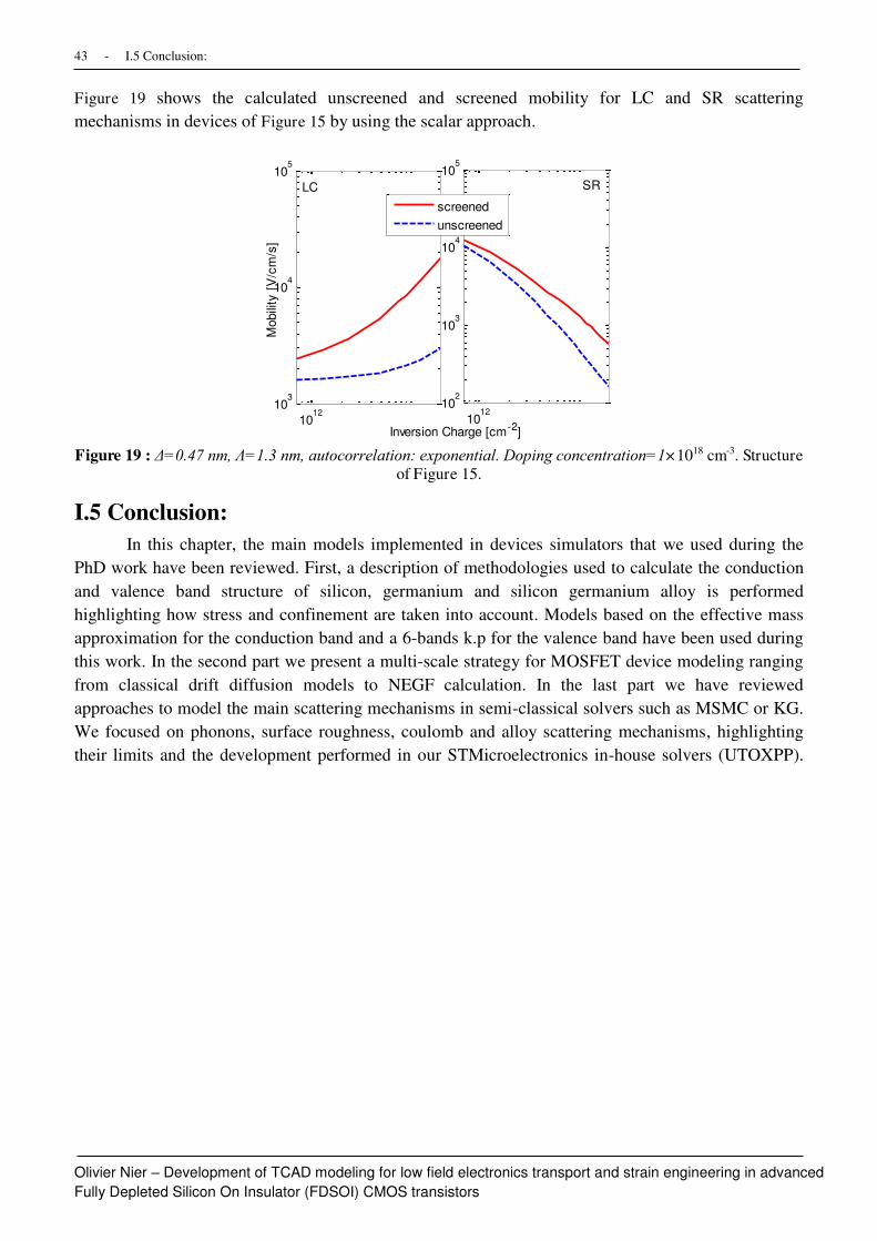
43 - I.5 Conclusion:
Olivier Nier – Development of TCAD modeling for low field electronics transport and strain engineering in advanced
Fully Depleted Silicon On Insulator (FDSOI) CMOS transistors
Figure 19 shows the calculated unscreened and screened mobility for LC and SR scattering
mechanisms in devices of Figure 15 by using the scalar approach.
Figure 19 : Δ=0.47 nm, Λ=1.3 nm, autocorrelation: exponential. Doping concentration=1×1018 cm-3. Structure
of Figure 15.
I.5 Conclusion:
In this chapter, the main models implemented in devices simulators that we used during the
PhD work have been reviewed. First, a description of methodologies used to calculate the conduction
and valence band structure of silicon, germanium and silicon germanium alloy is performed
highlighting how stress and confinement are taken into account. Models based on the effective mass
approximation for the conduction band and a 6-bands k.p for the valence band have been used during
this work. In the second part we present a multi-scale strategy for MOSFET device modeling ranging
from classical drift diffusion models to NEGF calculation. In the last part we have reviewed
approaches to model the main scattering mechanisms in semi-classical solvers such as MSMC or KG.
We focused on phonons, surface roughness, coulomb and alloy scattering mechanisms, highlighting
their limits and the development performed in our STMicroelectronics in-house solvers (UTOXPP).
1012
103
104
105
Mobili
ty [
V/c
m/s
]
1012
102
103
104
105
Inversion Charge [cm-2]
screened
unscreened
LC SR

44
Chapter 2:
Physics-based modeling of low field transport
in FDSOI transistors and comparison with
experiments
II.1 Introduction ................................................................................................................................................. 45
II.2 Advanced transport solvers comparison: Monte Carlo and Kubo Greenwood approaches compared
to NEGF simulations. ......................................................................................................................................... 45
II.2.1 Solvers description .................................................................................................................................. 46
II.2.2 Methodology of comparison of different approaches ............................................................................. 46
II.2.3 Advanced solvers comparison ................................................................................................................. 49
II.3 Split-CV mobility measurements in FDSOI structures: experimental results and calibration. ........... 54
II.3.1 Sample processed .................................................................................................................................... 54
II.3.2 Impact of the back bias ........................................................................................................................... 55
II.3.3 Impact of the interfacial layer thickness ................................................................................................. 57
II.3.4 Impact of the Temperature ...................................................................................................................... 59
II.3.5 Universal behavior of the mobility: extraction of the parameter η in FDSOI devices ............................ 59
II.4 Calibration for empirical solvers and comparison to measurements ..................................................... 62
II.4.1 Process simulation in TCAD ................................................................................................................... 62
II.4.2 TCAD empirical mobility model calibration .......................................................................................... 62
II.4.3 Comparison to Experimental data ........................................................................................................... 65
II.5 Conclusion .................................................................................................................................................... 67

45 - II.1 Introduction
Olivier Nier – Development of TCAD modeling for low field electronics transport and strain engineering in advanced
Fully Depleted Silicon On Insulator (FDSOI) CMOS transistors
II.1 Introduction
The aim of this chapter is twofold. In the first place, a comparison of the different approaches
currently available to model low field transport in advanced Fully Depleted SOI transistors is
performed. In the second place, the aim is to compare model accuracies to split CV mobility
measurements. Semi-classical approaches based on the momentum relaxation time (such as KG) or
based on the solution of the BTE (such as MSMC [46] [47]) have been widely used to calculate the
long channel mobility in high-k metal gate FDSOI devices [29] [34] [39] [41]. However, there are
only few examples in the literature of model comparisons on the same device [63]. Recently, P.
Palestri and al. [62] compared the mobility calculated using transport models ranging from drift-
diffusion to direct solutions of the BTE with the Monte Carlo method. Quite good agreements were
found at large inversion Ninv charges but discrepancies appear at low Ninv due to the different treatment
of phonon scattering in inversion layers. Moreover, a comparison between semi classical methods and
calculations based on NEGF approach is still missing. In fact, there are no commercial versions of
NEGF currently available including all scattering mechanisms. Moreover the modeling of long
channel transistor with NEGF is not straightforward and a methodology has been developed for that
purpose, as discussed later in this chapter. In consequence, in the first part of this chapter, the electron
and hole mobilities have been calculated using four different solvers: the STMicroelectonics in-house
solver (UTOXPP) [65], the commercial solver Sband from Synopsys [66], the MSMC solver from the
University of Udine [67] and TB_SIM [68], the NEGF solver from the CEA. Phonon, surface
roughness and coulomb (with charges at high-k/metal gate interface) limited mobilities have been
considered. The second part of this chapter has been dedicated to the comparison between simulations
and experiments, performed on state of the art FDSOI devices [69][70][75]. Using a large set of split-
CV measurements, the impact of the Equivalent Oxide Thicknesses (EOT), the back voltage and the
temperature have been investigated. We also reviewed important experimental and theoretical aspects
of the universal behavior of the mobility with respect to the effective field in FDSOI MOSFETs. Last
but not least, the capability of TCAD empirical models to reproduce theoretical and experimental
results has been investigated. Indeed, Technology Computer Aided Design (TCAD) support for
UTBB-FDSOI technology development can reduce cost and development time and also secure
technology choices. For efficient TCAD purposes, a preliminary identification of the mechanisms
responsible for transport degradation, as well as a calibration of empirical TCAD transport models, is
mandatory. The challenge in this area is being able to propose a more rigorous calibration of TCAD
mobility model on simulations rather than on experiments, while keeping the capability of reproducing
experiments in all possible measurement configurations.
II.2 Advanced transport solvers comparison: Monte Carlo and Kubo
Greenwood approaches compared to NEGF simulations.
The different methods to study the transport in advanced CMOS technology have been briefly
descried in chapter I. Before comparing mobility calculations, we present here the different tools used
during this thesis. All solvers are based on a multi-subbands (or quantum) approaches and this differs
from other approaches such as drift diffusion solvers.

46 - CHAPTER II. Physics-based modeling of low field transport in FDSOI transistors and comparison with
experiments
Olivier Nier – Development of TCAD modeling for low field electronics transport and strain engineering in advanced
Fully Depleted Silicon On Insulator (FDSOI) CMOS transistors
II.2.1 Solvers description
1) Multi-subbands Monte Carlo (MSMC):
The MSMC solver of the University of Udine includes scattering with phonons [47], surface
roughness (GPN model), coulomb and alloy scattering mechanisms (ionized impurities and remote
Coulomb) [47]. The screening can be accounted for using the scalar or the tensorial approach.
Concerning band structure models, the EMA is used for the conduction band calculation.
2) UTOXPP
UTOXPP is a self-consistent 1D Schrödinger-Poisson solver developed at STMicroelectronics [66].
The mobility is calculated using the Kubo-Greenwood formula presented in chapter I (equation 1.26)
for both electrons and holes. The solver includes scattering with phonons [47], surface roughness
(GPN model) [46], coulomb and alloy scattering mechanisms (ionized impurities and remote
Coulomb) [47]. The screening can be accounted for using the scalar or the tensorial approach. The
band structure models range from the non-parabolic EMA to 30 band k.p, including 2 band k.p and 6
band k.p.
3) Sband
Sband is a commercial self-consistent 1D Schrödinger-Poisson solver from Synopsys [65] coupled
with the Kubo-Greenwood formula to calculate the mobility for both electrons and holes. The solver
includes the same scattering mechanisms as in UTOXPP. The screening can be accounted for using
the scalar approach for surface roughness scattering and the scalar or tensorial approach for coulomb
scattering. The band structure is calculated thanks to the non-parabolic EMA or 2 band k.p models for
conduction band and 6 band k.p for the valence band.
4) TBSIM:
TB_SIM [68] is the NEGF solver from the CEA. In this code the NEGF equations are solved on a
finite difference grid, in a coupled space mode approach. The solver include scattering with phonons
using the Born approximation [38], “geometrical” surface roughness, local coulomb and remote
coulomb scattering mechanisms. The band structure is calculated using EMA or 2 band k.p for
conduction band and a 6 band k.p for the valence band.
II.2.2 Methodology of comparison of different approaches
Before starting the comparison between mobilities calculated with all solvers, let us put forth two
important points. First we discuss about the methodology of extraction of single mechanism limited
mobility, and then, the effective field definition in UTBB-FDSOI MOSFETs.
Extraction of phonon, coulomb, remote coulomb and surface roughness-limited mobility
The Matthiessen’s rule states that the inverse total mobility is the sum of the inverse of the partial
mobilities of each scattering mechanism:
な航痛墜痛暢 = な航牒張 + な航聴眺 + な航眺寵聴 (2.1)

47 - II.2 Advanced transport solvers comparison: Monte Carlo and Kubo Greenwood approaches compared to NEGF simulations.
Olivier Nier – Development of TCAD modeling for low field electronics transport and strain engineering in advanced
Fully Depleted Silicon On Insulator (FDSOI) CMOS transistors
It can be proved that [38] this widely used equation is exact only if 1) the scattering rates of all
mechanisms have the same dependence on energy, and 2) these mechanisms are independent one from
each other (no spatial correlations). The second condition usually holds for phonons, SR and RCS, but
the first one does not. Moreover, although the PH, RCS, LC and SR-limited mobilities can be
calculated using KG solvers through equation 2.2, in NEGF or MSMC simulations, these mobilities
cannot be extracted directly by turning off the phonon scattering mechanisms. As a consequence, an
“effective” mobility μ托, based on the Matthiessen’s rule is defined and used for the comparison between the different solvers:
航凋,勅捗捗−怠 = 航凋+牒張−怠 − 航牒張−怠 , (2.2)
A is the considered scattering mechanism: surface roughness or Coulomb scattering.
Quantitative errors, which compare the mobility directly extracted via KG simulations 航凋, and the
effective mobility 航凋,勅捗捗, have been calculated using the following expression [64]:
継 = 航凋,勅捗捗 − 航凋航凋 (2.3)
An error ranging from 20 to 12% is observed (Figure 20) for phonons + SR scattering mechanisms
which is consistent with simulations from Esseni et al. [64]. Concerning RC scattering, the error can
reach 80% which is of the order of magnitude than the error reported for local coulomb scattering
mechanism [64].
Figure 20 : Error E produced by the extraction of mobility components (surface roughness and remote
coulomb scattering) using the Matthiessen’s rule.
In Figure 21a, we can notice that the partial SR and RCS mobilities defined in equation 2.4 follow
Matthiessen’s rule much better than the usual, single mechanism partial mobilities (equation 2.1), as
testified in [38]. Indeed, Matthiessen’s rule holds within 1% in the whole density range (Figure 21b).
な航痛墜痛暢 = な航牒張 + な航聴眺,勅捗捗 + な航眺寵聴,勅捗捗 (2.4)
2 4 6 8 10 12
x 1012
-90
-80
-70
-60
-50
-40
-30
-20
-10
0
INVERSION CHARGE [cm-2
]
ER
RO
R ( (
M)
- ) [%
]
(M) RC
= (1/ PH+RC
-1/ PH
)-1
(M) RC
= (1/ PH+RC+SR
-1/ PH+SR
)-1
(M) SR
= (1/ SR+RC
-1/ PH
)-1

48 - CHAPTER II. Physics-based modeling of low field transport in FDSOI transistors and comparison with
experiments
Olivier Nier – Development of TCAD modeling for low field electronics transport and strain engineering in advanced
Fully Depleted Silicon On Insulator (FDSOI) CMOS transistors
Figure 21 : (a) Total KG mobility 侍嗣伺嗣皐札 = 侍�殺+傘三+三�傘皐札 (仔三�傘 = 惣. 宋 × 層宋層惣算仕−匝) compared with
Matthiessen’s rule 侍嗣伺嗣捌 from eq. 2.1 and 侍嗣伺嗣捌,蚕讃讃 from eq. 2.2. (b) Error induced by the Matthiessen rule 侍嗣伺嗣捌,蚕讃讃on the total mobility.
Of course, Matthiessen's rule might still break down at low enough temperature and in specific
systems, but its range of applicability is certainly broader using equation 2.4 as definition of the partial
mobility rather than a direct, single mechanism calculation (equation 2.1). This opens the way for a
more accurate modeling of the mobility in TCAD tools. Moreover it deserves to notice that TCAD
mobility models are based on the Matthiessen’s rule.
Discussion about the effective “mobility” field and the effective “electrostatic” electric field.
Since the seminal work by Takagi, in bulk transistors, theoretical and experimental mobilities are
usually shown as function of the effective field [44]. This representation has two main advantages.
First, the mobility curve versus effective field is independent of the substrate doping (leading to the so
called “universal mobility curve”). Second, it allows a simple comparison of different technologies
and with experimental data found in house or reported in the literature. In bulk devices, an effective
“mobility” field has been proposed:
Ea旦奪/奪脱脱奪淡丹 = Q辰 + ηQ辿ϵ託辿 (2.5)
where the value of (=0.5 for electrons, 0.3 for holes) has been taken from mobility experiments in
order to obtain the “universal” behavior [44]. Interestingly, when = 0.5, the effective field exactly
coincides with the average transverse “electrostatic” field seen by electrons but also by holes in the
channel, given by:
Ea旦奪担竪 = ∫ E炭岫�岻n岫�岻d�鐸SI待 ∫ n岫�岻d�鐸SI待 (2.6)
In the case of UTBB-FDSOI MOSFETs, the definition of the effective field has to be modified, in
order to take into account for the electric field at the back interface. The proper definition of an
effective field in the case UTBB-FDSOI MOSFETs for all possible bias configurations (including
volume inversion) is not easy and controversial [57] [58], especially in double gate device. However,
0 1 2 3 4 5 6 7 8 9
x 1012
350
400
450
500
550
600
650
Mo
bility [cm
2/V
.s]
Inversion charge [cm-2
]
tot
KG
1/tot
M,eff = 1/PH
+ 1/SR,eff
+1/RCS,eff
1/tot
M = 1/PH
+ 1/SR
+1/RCS
0 1 2 3 4 5 6 7 8 9
x 1012
0.1
0.2
0.3
0.4
0.5
0.6
0.7
0.8
0.9
1
Inversion charge [cm-2
]
tot
M -
tot
KG
)/ to
t
KG
[%
]

49 - II.2 Advanced transport solvers comparison: Monte Carlo and Kubo Greenwood approaches compared to NEGF simulations.
Olivier Nier – Development of TCAD modeling for low field electronics transport and strain engineering in advanced
Fully Depleted Silicon On Insulator (FDSOI) CMOS transistors
when the inversion layer is essentially produced by the front gate, the effective field is commonly
defined as [59]:
Ea旦奪/奪脱脱奪淡丹 = Q辰 + ηQ辿ϵ託辿 − ϵ誰淡ϵ託辿 VBT台拓X奪脱脱 (2.7)
with T台拓X奪脱脱 = 大S套+大BOX大S套 T台拓X + ∆, Q辿 the inversion charge, Q辰 the depletion charge (Q辰 = � NaT託I岻 and ∆≃1.5 nm accounts for the ground plane accumulation or depletion. In order to match equations 2.6
and 2.7, η has to be taken equal to η = 0.5 for both n- and pMOS devices in bulk [60] as well as in
FDSOI structures [61].
The validity of equation 2.7 can be seen in Figure 22. Indeed, in this figure the inversion charge is
plotted as a function of the average transverse field (calculated numerically) or as a function of the
effective field defined by equation 2.7, showing an excellent agreement for all applied back bias
(providing η= 0.5 for both electrons and holes).
Figure 22 : n- (left) and p- (right) FDSOI experimental electric field (equation 2.7) assuming η = 0.5 compared
to the simulated theoretical average field (equation 2.6). VB from -10 V to 10 V in steps of 2V. IL EOT =1.8
nm; T=300 K.
The concept of effective field will be used in the following section, to compare the different mobility
models. It will be also reconsidered in the section dedicated to the comparison with experiments. In
particular, the extraction of the parameter for n- and p FDSOI devices will be discussed in part
II.3.5.
II.2.3 Advanced solvers comparison
In order to compare the different solvers, the same device structure has been considered. This 1D
structure of the long channel FDSOI device (and material properties), used for the comparison is
illustrated in Figure 23. The device is essentially composed of an ultra-thin layer of silicon (10 nm or
less thick), between a thin Buried Oxide (BOX) (25nm) and a high-k gate stack. This latter oxide
includes an interfacial layer (of various thicknesses) and a thin layer of high-k (1.8 nm).
-1 0 1 20
0.5
1
1.5
2
2.5
3
3.5x 10
13
EFFECTIVE FIELD (MV/cm)
INV
ER
SIO
N C
HA
RG
E [cm-2
]
-1 0 1 20
0.5
1
1.5
2
2.5
3x 10
13
EFFECTIVE FIELD (MV/cm)
INV
ER
SIO
N C
HA
RG
E [cm-2
]
Theoritical Effective field: Eq. 2.3
Experimental effective field: Eq. 2.4
nMOS pMOS
0V<VB<10V -10V<VB<0V
-10V<VB<0V0V<VB<10V

50 - CHAPTER II. Physics-based modeling of low field transport in FDSOI transistors and comparison with
experiments
Olivier Nier – Development of TCAD modeling for low field electronics transport and strain engineering in advanced
Fully Depleted Silicon On Insulator (FDSOI) CMOS transistors
Figure 23 : Schematic of the simulated FDSOI devices. The comparison is done for surface roughness, phonons
and remote Coulomb scattering
Electrons
In this comparison a purely parabolic band has been considered for simplicity. Phonon scattering
parameters are listed in Table 7.
Phonon Type Coupling constant ℏ�使酸[meV]
intervalley f-type DtK= 0.3 108 eV/cm 18.96
intervalley f-type 2.0 108 47.4
intervalley f-type 2.0 108 59.03
intervalley g-type 0.5 108 12.06
intervalley g-type 0.8 108 18.53
intervalley g-type 11.0 108 62.04
intravalley DAC =14.6 eV 0
Table 7 : Phonons model parameters used for silicon taken from [85].
First of all, the phonon-limited mobility extracted at two different effective fields (0.08 and 0.6
MV/cm) is plotted in Figure 24 for silicon thicknesses varying from 2 nm to 10 nm. The expected non-
monotonic behavior is observed [41] and can be explained by two counteracting effects [42]:
- the form factor defined in equation 1.32 increases with decreasing TSi [42];
- below 10 nm, the electrons are progressively confined in the lowest unprimed subband which
features a lower conduction mass [41].
In this case, an excellent agreement between all solvers is obtained.
Figure 24 : Comparison of phonon-limited electrons mobility in FDSOI devices as a function of active layer
thickness.
2 3 4 5 6 7 8 9 10500
550
600
650
700
750
800
850
SILICON THICKNESS [nm]
PH
ON
ON
MO
BIL
ITY
[cm
2/V
s]
UTOX
NEGF: TB SIM
MSMC
0.6 MV/cm
0.08 MV/cm

51 - II.2 Advanced transport solvers comparison: Monte Carlo and Kubo Greenwood approaches compared to NEGF simulations.
Olivier Nier – Development of TCAD modeling for low field electronics transport and strain engineering in advanced
Fully Depleted Silicon On Insulator (FDSOI) CMOS transistors
In Figure 25a, the calculated SR-limited mobility as a function of the effective field using all solvers
has been reported for three different silicon thicknesses. The same parameters than in [34] have been
used for comparison: an exponential SR autocorrelation with RMS amplitude of Δ=0.47 nm and a
correlation length of Λ=1.3 nm. The mobility calculated with all solvers has been extracted using the same procedure (previously explained in part II.2.2) in order to avoid differences due to the extraction
method. Results obtained by the semi-classical solvers (sband, UTOX and MSMC) have been found in
good agreement, however not with the NEGF result. This is further depicted in Figure 25b, which
represents the SR-limited mobility as a function of the silicon thickness. The results of S. Jin [34], also
based on a semi-classical approach, but accounting for carrier density fluctuation and image charge
effects, have also been added on this Figure 25b. The disagreement between semi-classical methods
and NEGF might result from [38]: 1) the second-order perturbation theory (Fermi Golden Rule)
behind KG and MSMC; and 2) the approximations made in the treatment of SR in KG. It has been
shown in [38] that the Fermi Golden Rule seems to be valid for SR scattering so this overestimation of
the mobility seems to be due to assumptions behind the implemented SR model (Generalized Prange
Nee model) as described in Chapter I.
Figure 25 : Surface roughness-limited electrons mobility a) as a function of the effective field for TSi=2.6 nm,
4.0 nm and 7.0 nm. b) as a function of TSi extracted at Eeff= 0.08 and 0.77 MV/cm. (exponential SR
autocorrelation with Δ=0.47 nm; Λ=1.3 nm).
In Figure 26, the SR-limited mobility is compared between UTOXPP and Sband for various doping
concentrations at VB=0V and 8V. For high back biases (back gate inversion), a non-monotonic trend
is observed (Figure 26b and Figure 27) which is a consequence of scattering with surface roughness at
the back and front interfaces.
0.1 1
103
104
EFFECTIVE FIELD (MV/cm)
SR
MO
BIL
ITY
(cm2
/V-S
)
SBAND
UTOX
NEGF: TB SIM
MSMC
4nm
7nm
2.6nm
2 3 4 5 6 7 8 9
103
104
SILICON THICKNESS [nm]
SR
MO
BIL
ITY
[cm2
/Vs]
SBAND
UTOX
NEGF: TB SIM
MSMC
[Jin [2007]
0.77 MV/cm
0.08 MV/cm

52 - CHAPTER II. Physics-based modeling of low field transport in FDSOI transistors and comparison with
experiments
Olivier Nier – Development of TCAD modeling for low field electronics transport and strain engineering in advanced
Fully Depleted Silicon On Insulator (FDSOI) CMOS transistors
Figure 26 : SR-limited mobility as a function of the inversion charge calculated using Sband and UTOXPP for
different channel doping concentrations at VB=0V (a) and VB=8V (b). (Exponential auto-correlation with
∆=0.47 nm and Λ=1.3 nm).
Figure 27 : SR-limited mobility as a function of Eeff calculated for different channel doping concentration at
VB=0 and 8V.
In Figure 28, remote Coulomb scattering calculated with KG is compared to results obtained using
NEGF at two different back voltages (VB=0V and VB=8V). In this case, a quite good agreement is
found between the solvers.
Figure 28 : Remote-Coulomb-limited electron mobility as a function of the inversion charge for devices with
two different IL EOT: 1.0 nm and 4.0 nm. Nit = 5×1013 cm-2
1012
1013
0
2000
4000
6000
8000
10000
12000
14000
16000
Inversion charge [cm-2
]
SR
-lim
ite
d m
ob
ilit
y [c
m2/V
/s]
sband
UTOXPP
1e19 cm-3
1e18 cm-3
-1e19 cm-3
-1e18 cm-3
1e15 cm-3
1013
1000
2000
3000
4000
5000
6000
7000
8000
9000
10000
SR
-lim
ite
d m
ob
ilit
y [c
m2/V
/s]
Inversion charge [cm-2
]
sband
UTOXPP
Na = 1e19 cm
-3
Na = 1e15 cm
-3
Na = 1e18 cm
-3
-5 0 5 10 15 20
x 105
103
104
105
Effective field (V/cm)
SR
-lim
ite
d m
ob
ilit
y [c
m2/V
/s]
sband
UTOXPPfrom -1e19 to
1e19 cm-3
from -1e19 to 1e19 cm-3
VB = 0V
VB = 8V
0 5 10 15
x 1012
102
103
104
105
INVERSION CHARGE [/cm²]
MO
BIL
ITY
[cm
²/V
/s]
NEGF (VB=0V)
KG (VB=0V)
NEGF (VB=8V)
KG (VB=8V)
IL EOT=1.0nm
IL EOT=4.0nm

53 - II.2 Advanced transport solvers comparison: Monte Carlo and Kubo Greenwood approaches compared to NEGF simulations.
Olivier Nier – Development of TCAD modeling for low field electronics transport and strain engineering in advanced
Fully Depleted Silicon On Insulator (FDSOI) CMOS transistors
The Local Coulomb-limited mobility is compared between UTOXPP and Sband in Figure 29 for
various doping concentration, for VB=0V and 8V. Excellent agreements are found between the two
solvers.
Figure 29 : Local-Coulomb-limited electron mobility as a function of a) the effective field and b) the inversion
charge for various channel doping concentrations and for VB=0V and 8V. The metal gate stack consists in a
1.8 nm thick high-k material (ε=20) on top of a 1.2 nm thick SiON layer (ε=6.6).
Holes
In this study, the hole band structure has been calculated using a 3 bands k.p model with L, M and N
parameters from Table 3 (Δ=0). Parameters for the scattering mechanisms are listed in Table 8.
Phonon type Coupling constant ℏ�使酸[meV]
intravalley DtK= 15.0 * 108 eV/cm 62.0
intravalley DAC =10.2 eV 0
Surface roughness Δ [nm] Λ [nm] Autocorrelation
0.47 1.3 Exponential
Table 8 : Phonons and surface roughness mobility model parameters for holes.
The phonon-limited mobility is plotted as a function of the inversion charge for three different silicon
thicknesses (3.0, 5.0 and 7.0 nm) in Figure 30. The mobility calculated with KG solvers presents a
mobility compared to the results obtained with the NEGF solver.
Figure 30 : Comparison of phonon-limited holes mobility in FDSOI devices as a function of the inversion
charge for three different silicon thicknesses (3.0, 5.0 and 7.5 nm).
-4 -2 0 2 4 6 8 10 12
x 105
103
104
105
LC
-lim
ite
d m
obilit
y [c
m2/V
/s]
Effective field [V/cm]
sband
UTOXPP
Na = 1e19 cm
-3
Na = 1e18cm
-3
Na = 1e17 cm
-3
VB = 0V
VB = 8V
VB = 0V
VB = 8V
VB = 8V
VB = 0V
0 0.5 1 1.5 2 2.5
x 1013
103
104
105
LC
-lim
ite
d m
obilit
y [c
m2/V
/s]
Inversion charge [cm-2
]
sband
UTOXPP
Na = 1e17 cm
-3
Na = 1e19 cm
-3
Na = 1e18 cm
-3
VB = 8V
VB = 0V
VB = 8V
VB = 0V
VB = 8V
VB = 0V
1012
1013
60
80
100
120
140
160
180
INVERSION CHARGE [cm-2]
PH
MO
BIL
ITY
[cm
2/V
/s]
SBAND
NEGF
UTOXPP
7.5 nm
3.0 nm
5.0 nm

54 - CHAPTER II. Physics-based modeling of low field transport in FDSOI transistors and comparison with
experiments
Olivier Nier – Development of TCAD modeling for low field electronics transport and strain engineering in advanced
Fully Depleted Silicon On Insulator (FDSOI) CMOS transistors
In Figure 31, we reported the SR-limited mobility as a function of the inversion charge for three
different silicon thicknesses. A good agreement between UTOXPP, Sband and TBSIM can be
observed for TSi=7.5 nm. However, the conclusion is the same as for electrons: the mobility
degradation with TSi, observed with semi-classical solvers, is less pronounced compared to NEGF
simulations.
Figure 31 : Surface roughness-limited holes mobility as a function of the inversion charge for TSi=3.0 nm, 5.0
nm and 7.5 nm.
II.3 Split-CV mobility measurements in FDSOI structures:
experimental results and calibration.
In the previous section, we have compared the mobility calculated using semi-classical solvers
such as KG and MSMC to NEGF results. In the second part of this chapter, a comparison between
simulations and experiments is performed on UTBB-FDSOI structures. Using a large range of split-
CV measurements, the impact of the Equivalent Oxide Thicknesses (EOT), the back voltage and the
temperature have been investigated. We also reviewed important experimental and theoretical aspects
of the universal behavior of the mobility with respect to the effective field in FDSOI MOSFETs.
II.3.1 Sample processed
Devices have been processed on 300 mm SOI wafers with a 25 nm thick BOX (Figure 32). The oxide
stack is made of a 1.8 nm thick layer of high-k oxide (HfSiON) deposited on top of an SiON
interfacial layer (IL) with various EOT from 0.7 to 3.0 nm The final silicon channel thickness is 7.5
nm and the effective mobility was extracted using split-CV method on 0.9x0.9 µm² (WxL) devices
corrected from access resistances Raccess=2x60 Ω.µm. Measurements have been performed on n- and
p-type devices.
1012
1013
102
103
INVERSION CHARGE [cm-2]
SR
MO
BIL
ITY
[cm
2/V
/s]
SBAND
NEGF
UTOXPP7.5 nm
5.0 nm
3.0 nm

55 - II.3 Split-CV mobility measurements in FDSOI structures: experimental results and calibration.
Olivier Nier – Development of TCAD modeling for low field electronics transport and strain engineering in advanced
Fully Depleted Silicon On Insulator (FDSOI) CMOS transistors
Figure 32 : a) Front-end process flow for 28FDSOI technology. b) Cross-section of a FDSOI MOSFET
II.3.2 Impact of the back bias
The impact of voltage VB, applied at the back terminal, on the gate capacitance is shown in Figure 33
for both n- and pMOS devices. As previously demonstrated in [42], in the reverse regime (back
inversion), the capacitance is distorted and reaches a first level whose magnitude is related to the
active layer capacitance CSi in series with the oxide one Cinv. The capacitances obtained from all
solvers (only TCAD results are shown here) are added on the figure allowing an accurate calibration
of the EOT.
Figure 33 : Gate capacitance as a function of the gate voltage for various back biases ranging from -10V to
10V per steps of 2V in n- (a) and p-MOS (b) devices. Tinv=2.65 nm; TSi=7.5 nm; T=300 K. TCAD calibration
shown for VB=-8, 0 and 8V.
Figure 34a shows the threshold voltage (VTH) variation with VB for n- and pMOS devices. As can be
seen, the VTH can be shifted by -1.5 V to 1 V for VB with ranging from -10 V to 10 V. The
corresponding drain current measurement at various VB is shown in Figure 34b. We found out that the
sub-threshold slope remains almost unchanged with back bias (∆S/S<7%).
-1 0 1 2
0
2
4
6
8
10
12
14
16
x 10-3
GATE VOLTAGE [V ]
nM
OS
CA
PA
CIT
AN
CE
(F
/m2 )
-1 0 1 2
0
2
4
6
8
10
12
14
16
x 10-3
GATE VOLTAGE [V ]
pM
OS
CA
PA
CIT
AN
CE
(F
/m2 )
Experiments
TCAD simulations
VB < 0V
VB < 0V
VB > 0V
Cinv // CSi Cinv // CSi
VB > 0V
nMOS pMOS
[TS
i/ Si +
To
x/ ox]-1

56 - CHAPTER II. Physics-based modeling of low field transport in FDSOI transistors and comparison with
experiments
Olivier Nier – Development of TCAD modeling for low field electronics transport and strain engineering in advanced
Fully Depleted Silicon On Insulator (FDSOI) CMOS transistors
Figure 34 : Threshold voltage variation (reference at VB=0 V) as a function of the back bias in n- and pMOS
devices. Tinv=2.65 nm; TSi=7.5 nm; T=300 K.
The dependence of the mobility on inversion charge for various back biases for n- and pMOS is shown
in Figure 35. For a given inversion charge, an increase of the mobility is observed for VB>0 V in
nMOS and for VB<0 V in pMOS devices. In reverse region, a non-monotonic behavior of the mobility
is shown (not to be confused with the RC-limited contribution observed at lower density). This is
further depicted in Figure 36 which represents the mobility variation as a function of VB for fixed
inversion charge for both devices.
Figure 35 : Experimental effective mobility as a function of the inversion charge for various back biases
ranging from -10V to 10V in steps of 2V, in n- (a) and pMOS devices (b). Tinv=2.65 nm; TSi=7.5 nm; T=300 K.
Figure 37 shows the profile of the potential and the electron density in the channel simulated using
Poisson-Schrödinger solver (PS) for three front and back gate voltage conditions specified in Figure 36
(Ninv = 1 ×1013 cm-2). The application of a high positive VB induces a back gate inversion for nMOS
devices. No clear “volume” inversion regime is however reached as the majority of carriers are still
confined at front and back interfaces. This is expected since the silicon channel is too thick (TSi = 7.5
nm) to reach this regime [95]. The mobility enhancement can be explained by the shift of the inversion
charge centroid away from the front interface affecting surface roughness and the screening of the
Coulombic effect at the high-k/IL interface [38].
-10 -5 0 5 10-2
-1.5
-1
-0.5
0
0.5
1
1.5
2
VB [V]
VT
H(V
B)
- V
TH
(VB
=0
V)
[V]
TCAD
MeasurementsnMOS
pMOS
-2 0 210
-10
10-9
10-8
10-7
10-6
10-5
GATE VOLTAGE [V]
pM
OS
DR
AIN
CU
RR
EN
T [A
]
-2 0 210
-10
10-9
10-8
10-7
10-6
10-5
GATE VOLTAGE [V]
nM
OS
DR
AIN
CU
RR
EN
T [A
]
VB > 0V
VB > 0V VB < 0V
VB < 0V
nMOS pMOS
0 0.5 1 1.5 2 2.5
x 1013
0
50
100
150
200
250
300
350
400
450
500
INVERSION CHARGE [cm-2
]
nM
OS
MO
BIL
ITY
(cm2
/V/s
)
0 0.5 1 1.5 2
x 1013
0
20
40
60
80
100
120
140
INVERSION CHARGE [cm-2
]
pM
OS
MO
BIL
ITY
(cm
2/V
/s)
VB > 0V
pMOSnMOS
VB < 0V
VB > 0V
VB < 0V

57 - II.3 Split-CV mobility measurements in FDSOI structures: experimental results and calibration.
Olivier Nier – Development of TCAD modeling for low field electronics transport and strain engineering in advanced
Fully Depleted Silicon On Insulator (FDSOI) CMOS transistors
Figure 36 : Effective experimental mobility as a function of the back bias for various inversion densities:
Ninv=1×10¹³, 5×10¹² and 2×1012 cm-². IL EOT= 1.8 nm; TSi=7.5 nm; T=300K. Symbols represent biases
conditions whose density profiles are extracted in Figure 37: 1/ VB=-5 V, VG=2.0 V; 2) VB=0 V, VG=1.6 V; 3)
VB=5 V, VG=1.2 V.
Figure 37 : Simulated profile of the potential (a) and the electron density (b) in the channel for various biases
conditions using PS simulations): 1/ VB=-5 V, VG=2.0 V; 2) VB=0 V, VG=1.6 V; 3) VB=5 V, VG=1.2 V.
nMOS device, IL EOT= 1.8 nm. TSi=7.5 nm; T=300 K.
II.3.3 Impact of the interfacial layer thickness
The gate capacitance for three devices with physical IL thicknesses of 2.4 nm, 3.5 nm and 4.0 nm is
shown in Figure 38. The capacitances calculated with all solvers (only TCAD results are shown here)
are also added to the figure.
-10 -5 0 5 100
100
200
300
400
500
600
VB [V]
MO
BIL
ITY
[cm
2/V
/s]
Ninv=1e13cm-2
Ninv=5e12cm-2
Ninv=2e12cm-21)
2)
pMOS
3)
nMOS
0 2 4 6
x 10-3
1
2
3
4
5
6
7
8x 10
19
POSITION [µm]
De
nsity (
cm
- ²)
-5 0 5 10
x 10-3
-5
-4.5
-4
-3.5
-3
-2.5
PO
TE
NT
IAL
[e
V]
POSITION [µm]
VG=2V VB=-5V
VG=1.6V VB=0V
VG=1.2V VB=5V
OX Channel BOX
1)
2)
2)
1)
3)
3)

58 - CHAPTER II. Physics-based modeling of low field transport in FDSOI transistors and comparison with
experiments
Olivier Nier – Development of TCAD modeling for low field electronics transport and strain engineering in advanced
Fully Depleted Silicon On Insulator (FDSOI) CMOS transistors
Figure 38 : Gate capacitance as a function of the gate voltage for devices with different IL EOT varying from
0.7 nm to 3.0 nm.
The mobility variation with respect to the inversion charge for four structures with different IL EOT
(0.7, 1.8, 2.3 and 3.0 nm) is shown in Figure 39. A significant degradation of the mobility is observed
with decreasing IL. The degradation of the mobility in presence of high-k oxide is well known and can
be attributed to remote coulomb [76] [86] [87] [88], remote phonon [89] or remote surface roughness
scattering [90]. These scattering mechanisms are strongly dependent on the thickness of the interfacial
layer but it has been demonstrated in [88] that the remote phonon scattering mechanism is significant
for IL EOT<1 nm only. Concerning remote surface roughness scattering, there is a controversial
debate about its importance. Indeed, some groups suggest that it may degrade the mobility [91] [92]
but there is no publication demonstrating it by means of experimental data. Moreover, for IL EOT>1
nm, our simulations suggest that RC is the main mechanism responsible for the mobility degradation
(variation of the mobility with the IL EOT is well reproduced by considering RC only-Figure 53a).
Figure 39 : n- (a) and pMOS (b) experimental effective mobility as a function of the inversion charge for
structures with various IL physical thicknesses (VB=0 V).
0 0.5 1 1.5 20
0.005
0.01
0.015
0.02
0.025
GATE VOLTAGE [V ]
nM
OS
CA
PA
CIT
AN
CE
(F
/m2 )
Measurements
Simulations
0 0.5 1 1.5 20
0.005
0.01
0.015
0.02
0.025
GATE VOLTAGE [V ]
pM
OS
CA
PA
CIT
AN
CE
(F
/m2 )
IL EOT=0.7 nm
IL EOT=1.8 nm
IL EOT=2.3 nm
IL EOT=3.0 nm
IL EOT=2.3 nm
IL EOT=1.8 nm
IL EOT=0.7 nm
IL EOT=3.0 nm
0 5 10
x 1012
0
50
100
150
200
250
300
350
400
450
500
INVERSION CHARGE [cm-2
]
MO
BIL
ITY
(cm
2/V
/s)
0 5 10
x 1012
40
50
60
70
80
90
100
110
120
INVERSION CHARGE [cm-2
]
MO
BIL
ITY
(m
2/V
/s)
IL EOT=0.7 nmIL EOT=0.7 nm
IL EOT=1.8 nmIL EOT=1.8 nm
IL EOT=2.3 nmIL EOT=2.3 nm
IL EOT=3.0 nmIL EOT=3.0 nm

59 - II.3 Split-CV mobility measurements in FDSOI structures: experimental results and calibration.
Olivier Nier – Development of TCAD modeling for low field electronics transport and strain engineering in advanced
Fully Depleted Silicon On Insulator (FDSOI) CMOS transistors
II.3.4 Impact of the Temperature
The mobility has been plotted as a function of the inversion charge at various temperature for n-
(Figure 40) and p-type (Figure 41) devices. As already observed in bulk devices, the mobility strongly
decreases at high temperatures and it is mainly due to an increase of phonon scattering rates.
Figure 40 : Effective experimental mobility as a function of the inversion charge for various VB ranging from -
10 V to 10 V in steps of 2 V. nFDSOI device : IL EOT= 1.8 nm. T=233, 300 and 450 K.
Figure 41 : Effective experimental mobility as a function of the inversion charge for various VB ranging from -
10 V to 10 V in steps of 2 V. pFDSOI device : IL EOT= 1.8 nm. T=233, 300 and 450 K.
II.3.5 Universal behavior of the mobility: extraction of the parameter η in FDSOI devices
In previous part, the experimental mobility has been plotted as a function of the inversion charge. It is
however more convenient, for technology comparison, to plot it as a function of the effective field
using equation 2.7. This raises the question of the extraction of the parameter η. A recent paper has
shown that the value of η in FDSOI devices may be different from bulk values [97]. Although, this
parameter is usually extracted by adjusting experimental curves in order to get the best universal trend,
an alternative technique has been recently proposed, deducing η from the following formula [98]:
�聴沈潮彫 = �系長墜掴�系喋 − 系墜掴 ���� � = 岫項航勅捗捗/項撃捗直岻|��虹岫項航勅捗捗/ 項撃長直岻|�肉虹 (2.8)
0 1 2 3
x 1013
0
100
200
300
400
500
600
700
INVERSION CHARGE [cm-2]
0 0.5 1 1.5 2 2.5
x 1013
0
100
200
300
400
500
600
700
MO
BIL
ITY
(cm
2/V
/s)
0 1 2 3
x 1013
0
100
200
300
400
500
600
700
T=300 K T=450 K
VB > 0V
VB = 0VVB < 0V
VB < 0V
VB > 0V
VB = 0V
VB > 0V
VB = 0VVB < 0V
T=233 K
0 0.5 1 1.5 2
x 1013
0
20
40
60
80
100
120
140
160
180
200
INVERSION CHARGE [cm-2]
0 0.5 1 1.5 2
x 1013
0
20
40
60
80
100
120
140
160
180
200
MO
BIL
ITY
(cm
2/V
/s)
0.5 1 1.5 2
x 1013
0
20
40
60
80
100
120
140
160
180
200
T=300 K T=450 K
VB = 0V
T=233 K
VB > 0VVB > 0V
VB < 0V
VB < 0V
VB = 0V
VB < 0V
VB > 0V
VB = 0V

60 - CHAPTER II. Physics-based modeling of low field transport in FDSOI transistors and comparison with
experiments
Olivier Nier – Development of TCAD modeling for low field electronics transport and strain engineering in advanced
Fully Depleted Silicon On Insulator (FDSOI) CMOS transistors
This method is used to extract η at VB=0 V for various temperatures (Figure 42a), leading to η = 0.42 and 0.36 for n- and p- FDSOI devices respectively. This can also be seen in Figure 42b where η has been characterized for devices with various IL EOT.
Figure 42 : Extracted value of parameter η using Eq. 2.8 in n- and pFDSOI devices for various temperatures
(T=233, 300 and 450 K). nFDSOI device: IL EOT = 1.8 nm. The domain of validity corresponds to the strong
front inversion regime. VB=0 V.
Using these extracted values η = 0.42 and 0.36, the experimental mobility has been plotted as a
function of the effective field (Figure 43). It can be noticed that using these extracted parameters and
equation 2.7 for the definition of the effective field, the universal trend cannot be obtained on the
whole range of VB. Moreover, it ought to be noticed that equation 2.8 is valid only when the front
interface is in the strong inversion regime [98]. However it can be interesting to apply this equation
with reverse VB (VB>0 V for nFDSOI and VB<0 V for pFDSOI devices) since at high gate voltages
the front channel is also inverted. In Figure 44, η has been extracted for VB varying from -10 V to 10
V in n- and p- FDSOI devices. In the front inversion regime, η converge to the previously extracted values while in the back inversion regime, an increase of the coefficients with VB can be observed. As
expected when the front channel is not inverted, equation 2.8 is not valid and the extraction of η is not relevant.
Figure 43 : n- (left) and p- (right) FDSOI experimental effective mobility as a function of the effective field. VB
ranging from -10 V to 10 V in steps of 2 V. Effective field calculated using Eq. 2.7 (η=0.42 for nFDSOI and η=0.36 for pFDSOI). IL EOT = 1.8 nm. T=300 K.
0 0.5 1 1.5 2
x 1013
0.2
0.25
0.3
0.35
0.4
0.45
0.5
PA
RA
ME
TE
R
INVERSION CHARGE [cm2]
T=233 K
T=300 K
T=450 K
pMOS
= 0.36
nMOS
= 0.42
0.4 0.6 0.8 1 1.2 1.4 1.6 1.8 2
x 1013
0
0.05
0.1
0.15
0.2
0.25
0.3
0.35
0.4
0.45
0.5
PA
RA
ME
TE
R
INVERSION CHARGE [cm2]
IL EOT=3.0 nm
IL EOT=2.3 nm
IL EOT=1.8 nm
IL EOT=0.7 nm
pMOS
nMOS
-1 0 1 2100
150
200
250
300
350
400
450
500
EFFECTIVE FIELD (MV/cm)
MO
BIL
ITY
(cm
2/V
/s)
-1 -0.5 0 0.5 1 1.530
40
50
60
70
80
90
100
110
120
130
EFFECTIVE FIELD (MV/cm)
= 0.42
VB>0VB>0
VB<0
nMOS pMOS
VB<0
VB=0
= 0.36
VB=0

61 - II.3 Split-CV mobility measurements in FDSOI structures: experimental results and calibration.
Olivier Nier – Development of TCAD modeling for low field electronics transport and strain engineering in advanced
Fully Depleted Silicon On Insulator (FDSOI) CMOS transistors
Figure 44 : Extracted value of parameter η using Eq. 2.8 in a nFDSOI device for various VB ranging from -10
V to 10 V. IL EOT = 1.8 nm. T=300 K. In the front inversion regime (VB<0), η=0.42 while in the forward regime (VB>0), η varies significantly with VB.
There is another aspect to mention concerning the key assumption behind equation 2.8. This equation
is based on the assumption [98]:
岫∂μ奪脱脱/ ∂E奪脱脱岻|V党塔 = 岫∂μ奪脱脱/ ∂E奪脱脱岻|V唐塔 (2.9)
In order to check the validity of this formula, in Figure 45 the mobility has been plotted with respect to
the effective field sweeping VB at fixed VG and sweeping VG at VB=0 V. The condition described in
equation 2.9 is not satisfied at high Eeff. In order to get a better agreement, η also has been re-extracted
by brute-force numerical fitting, leading to the value of η=0.62 for nFDSOI and η=0.5 for pFDSOI devices. Results are shown in Figure 46.
Figure 45 : n- and p- FDSOI experimental effective mobility as a function of the effective field sweeping the
back terminal or the gate terminal. Eq.2.7 has been used for the evaluation of the effective field with η=0.42 for nFDSOI and η=0.36 for pFDSOI devices. IL EOT = 1.8 nm. T=300 K.
0.5 1 1.5 2
x 1013
0
0.2
0.4
0.6
0.8
1
PA
RA
ME
TE
R
INVERSION CHARGE [cm-2
]
nMOS
1V < VB < 10V
-10V < VB < 0V
Equation 2.5 not valid
0.6 0.8 1 1.2 1.4 1.6 1.8 2
x 1013
0
0.2
0.4
0.6
0.8
1
PA
RA
ME
TE
R
INVERSION CHARGE [cm-2]
pMOS
10V > VB > 0V
-1V > VB > -10V
Equation 2.5 not valid
-1 -0.5 0 0.5 1 1.5 20
50
100
150
200
250
300
350
400
450
MO
BIL
ITY
(cm
2/V
/s)
EFFECTIVE FIELD (MV/cm)
VG sweep @ VB=0V
VB sweep @ VG=1.0V
VB sweep @ VG=2.0V
VB sweep @ VG=2.5V
VB sweep @ VG=-2.5V
VB sweep @ VG=-2.0V
VB sweep @ VG=-1.5V
VB sweep @ VG=1.5V
nMOS
pMOS
VB sweep @ VG=-1.0V
VG sweep @ VB=0V

62 - CHAPTER II. Physics-based modeling of low field transport in FDSOI transistors and comparison with
experiments
Olivier Nier – Development of TCAD modeling for low field electronics transport and strain engineering in advanced
Fully Depleted Silicon On Insulator (FDSOI) CMOS transistors
Figure 46 : n- (left) and p- (right) FDSOI experimental effective mobility as a function of the effective field. VB
ranging from -10 V to 10 V in steps of 2 V. Effective field calculated using Eq. 2.7 (η=0.62 for nFDSOI and η=0.5 for pFDSOI). IL EOT = 1.8 nm. T=300 K.
A nearly universal trend for the mobility with respect to Eeff can be obtained only in a limited range of
VB. Indeed, in reverse VB conditions, there is no single value of η resulting in universal mobility
versus effective field curves. The coexistence of multiple channels and the difference of interfaces
(front and back) quality make difficult to apply the same procedure than in bulk devices for the full
range of gate and back voltages.
II.4 Calibration for empirical solvers and comparison to measurements
II.4.1 Process simulation in TCAD
An accurate description of the process steps is done using the commercial software Sentaurus Process
[66] from SYNOPSYS (Figure 47). In a first step the stress is considered as negligible as there is no
major stressor such as SiGe channel or SiGe source and drain, in 28FDSOI technology. The stress
model calibration will be studied in a second time for the 14FDSOI technology.
Figure 47 : TEM cross-section superimposed to a process simulation of a UTBB-FDSOI device.
II.4.2 TCAD empirical mobility model calibration
As already mentioned, carrier transport in TCAD softwares (all simulations shown here are performed
with Sentaurus Device –Sdevice [66]) is determined using empirical models which depend on a series
-1 -0.5 0 0.5 1 1.530
40
50
60
70
80
90
100
110
120
130
EFFECTIVE FIELD (MV/cm)
-1 0 1 2100
150
200
250
300
350
400
450
500
EFFECTIVE FIELD (MV/cm)
MO
BIL
ITY
(cm
2/V
/s)
= 0.62 = 0.5
nMOS pMOS
VB>0VB<0
VB<0
VB=0VB=0
VB>0

63 - II.4 Calibration for empirical solvers and comparison to measurements
Olivier Nier – Development of TCAD modeling for low field electronics transport and strain engineering in advanced
Fully Depleted Silicon On Insulator (FDSOI) CMOS transistors
of unknown parameters that have to be calibrated. Among electrostatic and transport models, one can
mention: 1) the density gradient-based quantum correction; 2) the model accounting for saturation of
carrier velocity with high fields and; 3) mobility models for each single scattering mechanisms
(phonon, local coulomb, remote coulomb, surface roughness...) which are then combined using the
Matthiessen’s rule (The syntaxes for all mobility models is shown in Annex 2). It is important to
notify that these mobility models depend on the “local” electric field or the “local” carrier density and neglect non local effects such as the channel thickness. Consequently, additional mobility models are
introduced to emulate these non-local effects. A recent model accounting for the mobility degradation
in thin channel at both front and back interfaces has been developed in [99]. Details about this model
are well documented in [100] and the parameters have been carefully calibrated in [100]. This
calibration is used in the present study. In the part below let us give details about some of the mobility
models.
- The surface roughness-limited mobility is given by:
μ託琢 = 峭岫F⊥/F嘆奪脱岻代∗ げ + F⊥戴η 嶌−怠 (2.10)
A calibration of the SR parameters was mandatory to better reproduce measurements (げ = に.の × など怠腿
cm²/Vs, η = な × など泰待 V²/cm/s for nMOS and げ = ね.など × など怠泰 c�²/V�, η = の.ぱに × など戴怠 V²/cm/s
for pMOS in equation 2.10).
- The remote Coulomb-limited mobility was modeled using the following equation [100]:
μ琢大 = μ怠岫な + 岫c/c担嘆a樽坦岻旦岻岾N大N待峇遅態 . D (2.11)
with D = e�� 岫− 淡狸冬r套t岻. x is the distance from high-k/IL interface, N大 is the negative or positive
interface charge density, c is the local carrier concentration in the channel and the other terms are
fitting parameters.
- The carrier bulk mobility, i.e. phonon and coulomb-limited mobility is introduced through the
Philips unified mobility model proposed by Klaassen [96]
な航懲鎮銚銚鎚鎚勅津 = な航椎ℎ + な航鎮頂, (2.12)
where the phonon component is expressed as:
μ丹竪 = μ鱈a淡 ( TぬどどK )−馳套 (2.13)
Holes and electrons parameters are listed in Table 9. The local coulomb component may be further
represented as a composition of two terms μ狸達 = μI択 + μI大 with
μI択 = μ鱈a淡態μ鱈a淡 − μ鱈辿樽 (N琢醍題,怠NII ) ( TぬどどK )−戴α−怠.泰, (2.14)

64 - CHAPTER II. Physics-based modeling of low field transport in FDSOI transistors and comparison with
experiments
Olivier Nier – Development of TCAD modeling for low field electronics transport and strain engineering in advanced
Fully Depleted Silicon On Insulator (FDSOI) CMOS transistors
and
μI大 = μ鱈a淡 μ鱈辿樽μ鱈a淡 − μ鱈辿樽 |n − �NII | ( TぬどどK )待.泰 (2.15)
Parameter Electrons (arsenic) Electrons
(phosphorus)
Holes (boron) Unit 侍仕�� 1417 1414 470.5 cm2/Vs 侍仕餐仔 52.2 68.5 44.9 cm2/Vs 飼餐 2.285 2.285 2.247 1 錆三撮擦,層 9.68×10¹⁶ 9.2×10¹⁶ 2.23×1017 cm-3 � 0.68 0.711 0.719 1
Table 9 : Parameters for Philips unified mobility model for electrons and holes [100].
Figure 48 : PH + LC and LC-limited mobility determined using Philips unified mobility model.
The results for the model for local coulomb-limited mobility are illustrated as a function of the doping
concentration in Figure 48. Then, the calibrated remote Coulomb-limited mobility model (equation.
2.11) is compared to KG results. Figure 49 shows the variation of the nMOS RC mobility with respect
to the inversion charge for various high-k/IL interface charge densities (Figure 49a) and for various IL
EOT (Figure 49b). The calibrated empirical model reproduces well the mobility determined with KG
solvers. Similarly, RC-limited mobility has also been calibrated for pMOS in Figure 50.
1014
1016
1018
1020
102
103
104
Doping concentration [cm-3]
MO
BIL
ITY
[cm
2/V
/s]
Electrons
Holes
LC only
PH + LC

65 - II.4 Calibration for empirical solvers and comparison to measurements
Olivier Nier – Development of TCAD modeling for low field electronics transport and strain engineering in advanced
Fully Depleted Silicon On Insulator (FDSOI) CMOS transistors
Figure 49 : nMOS effective remote Coulomb-limited electron mobility in FDSOI devices as a function of the
inversion charge. KG and TCAD simulations are performed a) for various high-k/IL interface charge density in
a device with IL EOT=1.8 nm and b) for various IL EOT for a fixed interface charge density C=5× 層宋層惣 cm-2.
Tsi=7.5 nm; T=300 K. TCAD model parameters: μ層 = 想操惣 cm²/V/s, 算嗣司�仔史 = 層 × 層宋層掻 cm-3,児 = 層. 想, 雌匝 =層, 残算司餐嗣 = 層. 匝捜 × 層宋−挿 算仕. Phonons parameters of Table 7 for KG solvers.
Figure 50 : Same as Figure 49 but for holes. TCAD models parameters: μ層 = 想捜想 cm²/V/s, 算嗣司�仔史 = 層 × 層宋層掻
cm-3, 児 = 層. 掃, 雌匝 = 層, 残算司餐嗣 = 層. 捜 × 層宋−挿 算仕.
II.4.3 Comparison to Experimental data
In order to investigate the accuracy of calibrated TCAD models, the total mobility for nMOS is then
simulated using TCAD and KG solvers (parameters in Table 10) varying the IL EOT (Figure 51a) and
the temperature of the device (Figure 51b).
Band structure phonon Surface roughness Remote Coulomb
Electron parabolic band
structure
Parameters of
Table 7
Exponential Autocorrelation
ΔSR=0.47 nm and ΛSR=1.3 nm.
Scalar Lindhard screening.
Tensorial Lindhard screening.
Charge density at high-k/IL
interface: 3×1013 cm-2.
Hole six-bands k.p
model
Parameters of
Table 8
Exponential Autocorrelation
ΔSR=0.40 nm and ΛSR=1.3 nm.
Scalar Lindhard screening.
Tensorial Lindhard screening.
Charge density at high-k/IL
interface: 6×1013 cm-2.
2 4 6 8 10
x 1012
102
103
104
105
106
INVERSION CHARGE [cm-2
]
RC
mo
bility [cm
²/V
/s]
KG simulations
TCAD simulations
2 4 6 8 10
x 1012
102
103
104
105
INVERSION CHARGE [cm-2
]
RC
mo
bility [cm
²/V
/s]
C=5e13cm-² IL EOT =1.8 nm
IL EOT =3.0 nm
IL EOT =0.7 nm
C=1e12cm-²
C=5e12cm-²
C=1e13cm-²
C=5e13cm-²
IL EOT =1.8 nm
0 2 4 6
x 1012
102
103
104
RC
mo
bility [cm
²/V
/s]
INVERSION CHARGE [cm-2
]
0 2 4 6
x 1012
102
103
104
105
106
INVERSION CHARGE [cm-2
]
RC
mo
bility [cm
²/V
/s]
KG simulations
TCAD simulations
C=5e13cm-²
IL EOT =1.8 nm
C=1e13cm-²
C=5e12cm-²
IL EOT =1.8 nm
IL EOT =0.7 nm
IL EOT =3.0 nm

66 - CHAPTER II. Physics-based modeling of low field transport in FDSOI transistors and comparison with
experiments
Olivier Nier – Development of TCAD modeling for low field electronics transport and strain engineering in advanced
Fully Depleted Silicon On Insulator (FDSOI) CMOS transistors
Table 10 : Simulation parameters for KG solvers.
Concerning nMOS, a charge density of 3× など怠戴 cm-2 at high-k/IL interface is used to fit experimental
data and excellent agreements are found between solvers and experimental data. This charge density
theoretically leads [88] to a variation of VTH of nearly 0.45 V.
Figure 51 : n-MOS mobility as a function of the inversion charge a) for structures with various IL EOT or b) at
different temperatures. Comparison between TCAD, KG solvers and experiments.
These simulations have been also performed for pMOS devices, see Figure 52, using a charge density
of 6×1013 cm-2 at high-k/IL interface. In TCAD, the slight underestimation of the mobility variation
with temperature can be due to the fact that our remote coulomb and surface roughness-limited
mobility models neglect the variation with the temperature.
Figure 52 : p-MOS mobility as a function of the inversion charge for structures with various IL EOT a) or at
different temperatures b) Comparison between TCAD, KG solvers and experiments.
The total mobility is then extracted as a function of the IL EOT, at Ninv = 2× など怠戴 cm-2 (Figure 53a).
Good agreement is found for IL EOT>1 nm for both devices. The degradation of the mobility with the
IL thickness is well captured by considering remote Coulomb scattering only. This tends to suggest
that remote phonon and remote surface roughness have a negligible impact for IL EOT>1 nm.
0 5 10 15
x 1012
100
200
300
400
500
600
700
800
900
INVERSION CHARGE [cm-2
]
MO
BIL
ITY
(cm
2/V
/s)
Measurements
KG
TCAD
T=300K
IL EOT=3.0 nm IL EOT=1.8 nm
IL EOT=0.7 nm
0 5 10 15
x 1012
100
200
300
400
500
600
700
800
900
INVERSION CHARGE [cm-2
]
MO
BIL
ITY
(m
2/V
/s)
Measurements
KG
TCAD
T=300K
T=450K
T=233K
IL EOT=1.8 nm
0 2 4 6 8 10
x 1012
40
50
60
70
80
90
100
110
120
130
140
150
INVERSION CHARGE [cm-2
]
MO
BIL
ITY
(m
2/V
/s)
Measurements
KG
TCAD
IL EOT=0.7 nm
IL EOT=3.0 nm
IL EOT=1.8 nm
2 4 6 8 10 12 14
x 1012
0
20
40
60
80
100
120
140
160
180
200
INVERSION CHARGE [cm2]
MO
BIL
ITY
(cm
2/V
/s)
Measurements
KG
TCAD
T=233K
T=300K
IL EOT=1.8 nm

67 - II.5 Conclusion
Olivier Nier – Development of TCAD modeling for low field electronics transport and strain engineering in advanced
Fully Depleted Silicon On Insulator (FDSOI) CMOS transistors
Figure 53b illustrates the variation of the mobility with the temperature for various inversion charges
and for n- and pMOS. The mobility degradation (due to the increase of phonon scattering) with
increasing temperatures is well reproduced by simulations for both devices.
As an ultimate benchmark, the variation of the mobility with VB is accurately accounted for, as
testified by Figure 54. As can be seen, the experimental behavior (depicted in Figure 36) is well
captured by KG solvers but also by TCAD simulations.
Figure 53 : n- and pMOS mobility extracted at fixed inversion density as a function of a) the IL EOT b) the
Temperature. Comparison between TCAD, KG solvers and experiments.
Figure 54 : Simulated effective mobility as a function of the back bias for various inversion densities: Ninv=1×層宋13 and 2× 層宋12 cm-². Tinv=2.65 nm; TSi=7.5 nm; T=300 K.
II.5 Conclusion
In the first part of this chapter the electron and hole mobilities have been calculated using four
different solvers: the STMicroelectonics in-house solver (UTOXPP), the commercial solver Sband
from Synopsys, the MSMC solver from the University of Udine and TB_SIM, the NEGF solver from
the CEA. Concerning electrons mobility, good correlations were found between all solvers comparing
phonons and RC-limited mobilities. However, due to assumptions behind the GPN model, semi-
classical solvers (KG and MSMC) strongly overestimate the SR-limited mobility compared to NEGF.
The comparison of holes mobility showed a clear underestimation of the phonon-limited mobility
using KG solvers compared to NEGF and a different dependence of SR-limited mobility with the
silicon thickness.
0.5 1 1.5 2 2.5 3 3.550
100
150
200
250
300
350
400
450
500
550
600
IL EOT [nm]
MO
BIL
ITY
[cm
2/V
/s]
Exp TiN/HfSiON (TSi
=7.5 nm)
KG
TCAD
nMOS
pMOS
250 300 350 400 4500
100
200
300
400
500
600
TEMPERATURE [K]
MO
BIL
ITY
[cm
2/V
/s]
Exp TiN/HfSiON (TSi
=7.5 nm)
KG
TCAD
2e12 cm-2
nMOS
1e13 cm-2
pMOS
2e12 cm-2
1e13 cm-2
-10 -5 0 5 100
100
200
300
400
500
600
VB [V]
MO
BIL
ITY
[cm
2/V
/s]
Lines: KG
Symbols: TCAD
Ninv=1e13cm-2
Pinv=1e13cm-2
Pinv=2e12cm-2
Ninv=2e12cm-2

68 - CHAPTER II. Physics-based modeling of low field transport in FDSOI transistors and comparison with
experiments
Olivier Nier – Development of TCAD modeling for low field electronics transport and strain engineering in advanced
Fully Depleted Silicon On Insulator (FDSOI) CMOS transistors
The second part of this chapter has been dedicated to the comparison between simulations and
experiments, performed on state of the art FDSOI devices. Using a large range of split-CV
measurements, the impact of the Equivalent Oxide Thicknesses (EOT), the back voltage and the
temperature have been investigated. In the last part, we showed that, after being calibrated on
advanced transport solvers, TCAD empirical models can accurately reproduce experimental results.
This enables accurate and efficient TCAD simulations of UTBB FDSOI MOSFETs in state of the art
CMOS technology.

69
Chapter III:
Mechanical simulations of the process-induced
stress in 14FDSOI MOSFETs and comparison
with nanobeam diffraction strain
measurements
III.1 Introduction ................................................................................................................................................ 70
III.2. Methodology for mechanical stress modeling ......................................................................................... 70
III.2.1 Generality about stress and strain tensors .............................................................................................. 71
III.2.3 Boundary conditions .............................................................................................................................. 73
III.2.4 Material properties for mechanical stress simulations ........................................................................... 75
III.2.5 Process-induced stress ........................................................................................................................... 79
III.3 Strain measurement techniques ................................................................................................................ 82
III.4 TCAD Stress-dependent mobility models. ............................................................................................... 83
III.5 Conclusion ................................................................................................................................................... 91

70 - CHAPTER III. Mechanical simulations of the process-induced stress in 14FDSOI MOSFETs and comparison
with nanobeam diffraction strain measurements
Olivier Nier – Development of TCAD modeling for low field electronics transport and strain engineering in advanced
Fully Depleted Silicon On Insulator (FDSOI) CMOS transistors
III.1 Introduction
As the happy scaling era is now finished since a long time, boosters have become more and more
important in order to maintain the historical performance improvement. Providing a low-cost and low-
risk solution, strain engineering is one of the dominant technique to enhance device performance
maintaining the traditional MOSFET manufacturing process flow. The strain technologies can be
divided into two groups (Figure 55): the global techniques where the stress is introduced into the whole
wafer, and local techniques, where stress is delivered to each transistor separately and independently.
Local stress techniques to enhance MOSFETs performance was first incorporated by Ito et al. [101]
and Shimizu et al. [102] who used a contact etch-stop layer (CESL) or by Gannavaram et al. [103]
who used SiGe source and drain region in the early 2000s. Since the 90-nm technology node, uniaxial
stress was successfully integrated to the mainstream MOSFET process flow to improve device
performance. Global stress techniques such as strained SiGe channel (epitaxied SiGe layer on Si
substrate or SiGe layer formed by condensation [104]) or “strained Silicon On Insulator” (sSOI) [105],
are also current technique to enhance carriers mobilities in MOSFETs. Combining these techniques,
the stress in the channel can reach values between -1 and -2 GPa (uniaxial or biaxial) leading to drastic
changes of the mobility (e.g. by a factor of 2.5 to 3 for <110> oriented-channel p-type MOSFET)
[106]. Consequently, in TCAD, the prediction of the performance of strained-Si UTBB FDSOI
MOSFETs requires an accurate modeling of the stress profile in the transistor but also of the impact of
stress on transport properties. The aim of this chapter is twofold. First an accurate description of the
methodologies used during this thesis to model stress induced by the process flow is performed.
Simulations are compared to nanobeam diffraction (NBD) strain measurements. The second aim is to
study and calibrate (on advanced transport solvers) available TCAD models to efficiently account for
the influence of stress on mobility in a large range of stress (up to 2GPa).
Figure 55 : Classification of stress techniques.
In the first part of this chapter, we review the methodologies to calculate the mechanical stress in
FDSOI transistors using a solver based on the finite difference method (Sprocess from SYNOPSYS).
We focus on the description of the boundary conditions, materials mechanical behaviors and the
process-induced stress. Then, in the second part, we presented an accurate description, study and
calibration of TCAD stress-dependent mobility models.
III.2. Methodology for mechanical stress modeling
The modeling of the mechanical stress using the finite difference method is usually performed in four
different steps. First, the boundary conditions for the equations of mechanics are defined for each side
of the simulation domain (Dirichlet or Neumann boundary conditions). Second, mechanical properties

71 - III.2. Methodology for mechanical stress modeling
Olivier Nier – Development of TCAD modeling for low field electronics transport and strain engineering in advanced
Fully Depleted Silicon On Insulator (FDSOI) CMOS transistors
and their rheological behaviors are fixed for each material. This mainly consists in setting the
relationship between stresses and strains (elastic, viscous, plastic, viscoelastic laws). Third, all
elementary steps of the process flow are described (epitaxy, deposit, etching, oxidation, thermal
anneal…) and finally, the resolution of the equations of mechanics is done at each point of the
simulation mesh. In this section, we review the main approaches used during this thesis for mechanical
stress simulations in FDSOI devices.
III.2.1 Generality about stress and strain tensors
Expression of the stress tensor
A mechanical stress represents a force per unit area and is expressed in Pa or N/m2 in the international
system. By convention, a tensile stress component is positive and a compressive stress component is
negative. In an infinitesimal cubic volume element (represented in Figure 56), the stress is described by
a second-rank stress tensor σ辿棚 which can be expressed as:
σ辿棚 = [�掴掴 �掴槻 �掴佃�槻掴 �槻槻 �槻佃�佃掴 �佃槻 �佃佃] (3.1)
Stress components �沈沈 are normal stress components and stress �沈珍 with 件 ≠ 倹 are shear stress
components.
Figure 56 : Definition of the stress tensor components. The first subscript refers to the direction normal to the
face on which the stress is applied. The second subscript corresponds to the direction of the stress.
At equilibrium, the stress tensor σ辿棚 is symmetrical (σ辿棚 = σ棚辿, fo� 件 ≠ 倹岻 [129] and reduces to six
independent components. Thus, it can be simplified in the following vector:
σ辿棚 = { �掴掴�槻槻�佃佃�掴槻�槻佃�掴佃}
(3.2)
Each tensor can be decomposed in a sum of two tensors: a hydrostatic part ([σ辿棚]竪岻 which describes the
material behavior in the case of a pure volume change and a deviatoric part ([σ辿棚]辰岻 which describes an

72 - CHAPTER III. Mechanical simulations of the process-induced stress in 14FDSOI MOSFETs and comparison
with nanobeam diffraction strain measurements
Olivier Nier – Development of TCAD modeling for low field electronics transport and strain engineering in advanced
Fully Depleted Silicon On Insulator (FDSOI) CMOS transistors
arbitrary stress leading to the distortion of the material without volume change. These two tensors can
be described as
σ辿棚竪湛辰 = [�ℎ槻鳥 ど どど �ℎ槻鳥 どど ど �ℎ槻鳥] with �ℎ槻鳥 = 痛追岫σ套宕岻戴 = �猫猫+ �熱熱+ �年年戴 (3.3)
and σ辿棚辰奪旦 = σ辿棚 − σ辿棚竪湛辰
so σ辿棚辰奪旦 = [ 態�猫猫−�熱熱− �年年戴 �掴槻 �掴佃�槻掴 態�熱熱−�猫猫− �年年戴 �槻佃�佃掴 �佃槻 態�年年−�猫猫− �熱熱戴 ]
(3.4)
It is important to notice that the rheological behaviors of these two tensors can be treated differently in
simulation as explained later in the manuscript.
Strain tensor:
Identically to the stress tensor, the strain tensor can be defined as
ϵ辿棚 = [香掴掴 香掴槻 香掴佃香槻掴 香槻槻 香槻佃香佃掴 香槻掴 香佃佃] (3.5)
and simplified in a vector form as:
ϵ辿棚 = { 香掴掴香槻槻香佃佃香掴槻香槻佃香掴佃}
(3.6)
with 香沈珍 = 怠態 岫�通乳�掴日 + �通日�掴乳岻 項憲 is an infinitesimal vector deformation due to the stress on a infinitesimal distance 項捲.
The strain tensor can also be decomposed in hydrostatic and deviatoric parts:
ϵ辿棚 = ϵ辿棚竪湛辰 + ϵ辿棚辰奪旦 (3.7)
The modifications of the electrical properties of a material are governed by the strain tensor. In
particular, concerning the band structure, a hydrostatic stress modifies the lattice parameter only
leading to a uniform shift of all the energy bands as described in chapter I. This component does not
modify the bands population neither their effective mass but can lead to modification of the band gap.
In contrast, the deviatoric component breaks the symmetry of the crystal leading to strong
modifications of the band structure (band population, effective mass…).

73 - III.2. Methodology for mechanical stress modeling
Olivier Nier – Development of TCAD modeling for low field electronics transport and strain engineering in advanced
Fully Depleted Silicon On Insulator (FDSOI) CMOS transistors
III.2.3 Boundary conditions
Boundary conditions for 2D simulations
Common boundary conditions (BC) are of two types: Dirichlet and Neumann conditions. Dirichlet BC
fixes the value of the unknown solution (i.e. the displacement) on the side where it is applied whereas
Neumann BC forces the derivative of the solution (i.e. the velocity) to be constant.
Figure 57 : Main boundary conditions (BC) in 2D. Left) “Free” BC that implies a zero normal stress on each side. Right) Dirichlet BC applied on each side of the simulation domain. (1) corresponds to a fixed point and
(2) restricts the displacement to one direction.
Figure 57 shows two available configurations for BC. In the first case Neumann conditions are applied
on the two sides of the simulation domain making them “free” (Figure 57a). This configuration is
usable if the left and right sides of the simulation domain correspond to the physical limits of the
structure. In the second case, Dirichlet conditions are applied on each side of the simulation domain
(Figure 57cb). This condition imply a zero velocities in the direction perpendicular to the boundary
planes. Note that all configurations require a fixed point as show in Figure 57. During this thesis, we
applied the second configuration for all simulations.
Assumptions for 2D simulations:
In FDSOI technology, due to the incorporation of SiGe alloy for pMOSFET channel, the stress is
biaxial and can reach values between -1 and -2 GPa which can consequently change the mobility.
Moreover, due to layout effects and stress relaxation (explained more in details in chapter IV), the
stress in the width direction strongly depends on the dimension of the structure as testified in Figure
58. Thus, three-dimensional simulations should be performed to account for all these effects but are
more CPU time consuming. In two-dimensional simulations, the third direction can be treated within
two different approximations: a) in the “plane strain” analysis, the width is considered as infinite and no relaxation of the stress occurs; b) in the “plane stress” analysis, the width is considered as very small, so the stress component in this direction is null. Consequently, an intermediate solution is
needed to emulate the stress relaxation due to layout effects in 2D. All 2D simulations are performed
under plane strain assumption and the stress in the width direction is directly set to the “relaxed values” of Figure 58 (after Shallow Trench Isolation –STI- process steps) instead of the theoretical
value given by the germanium concentration in the channel (equation 3.21 and red curve in Figure 58).
This technique allows to emulate the relaxation of the stress in the width direction.
(1) (2)
Vx=0 Vx=0

74 - CHAPTER III. Mechanical simulations of the process-induced stress in 14FDSOI MOSFETs and comparison
with nanobeam diffraction strain measurements
Olivier Nier – Development of TCAD modeling for low field electronics transport and strain engineering in advanced
Fully Depleted Silicon On Insulator (FDSOI) CMOS transistors
Figure 58 : Evolution of the stress with the width dimension. This stress value corresponds to the mean stress in
the channel after the STI process steps.
This method assumes that the relaxation of the stress in the width direction do not influence the stress
profile in the length direction: there is no or a low correlation between stress profiles in these two
directions. To check this assumption, we performed 3D simulations on four different structures with
varying dimensions as represented in Figure 59. A 2D cut in the plane perpendicular to the width
direction is realized (Figure 60a) and then the longitudinal and transversal stresses are extracted along
the channel direction (1D cut in the channel shown in Figure 60b). In Figure 61a, we can notice that a
strong degradation of the transversal stress (σw) occurs for the two thinnest structures (W=0.06 µm).
Figure 61b shows that this relaxation of the stress in the W direction has a low influence on the stress
profile in the L direction, so the assumption is validated.
Figure 59 : 3D TCAD simulations of FDSOI devices with varying dimensions after STI process steps.

75 - III.2. Methodology for mechanical stress modeling
Olivier Nier – Development of TCAD modeling for low field electronics transport and strain engineering in advanced
Fully Depleted Silicon On Insulator (FDSOI) CMOS transistors
Figure 60 : a) 3D TCAD simulations of the longitudinal stress in the device. The dashed lines represent the
different 2D cuts of the structure. (b) 2D cut of the device. The dashed line represents the 1D cut of the
structure along the channel.
Figure 61 : Simulation of the (a) transversal and (b) longitudinal stress profile in the channel. Profile of Figure
60.
III.2.4 Material properties for mechanical stress simulations
State of the art semiconductors technologies require the use of several thin film materials with varying
mechanical properties (semiconductor, oxides, metals…). The rheological behavior of these materials
(i.e. the relation between stress and strain) and their mechanical properties must be described and
defined before each simulation. In this part, we define the most widely encountered material
rheological behaviors in microelectronics, namely elastic, viscoelastic and plastic laws.
Linear elasticity:
A large number of materials follow the elasticity law at low stress value. This behavior results in a
linear relation between the strain of the material and the applied stress. Usually represented as a spring
with a rigidity E (Figure 62), for isotropic material such as amorphous materials (silicon oxide, silicon
nitride), the Hooke’s law is written as:
σ = E ϵ (3.8)
with E the Young modulus.

76 - CHAPTER III. Mechanical simulations of the process-induced stress in 14FDSOI MOSFETs and comparison
with nanobeam diffraction strain measurements
Olivier Nier – Development of TCAD modeling for low field electronics transport and strain engineering in advanced
Fully Depleted Silicon On Insulator (FDSOI) CMOS transistors
Figure 62 : Schematic of the uniaxial linear elasticity.
For anisotropic materials, such as silicon and germanium, the Hooke’s law relates that the stress tensor
is linearly related to the strain tensor trough the stiffness matrix 系沈珍 :
σ辿棚 = C辿棚谷狸 ϵ谷狸 (3.9)
and in return, the strain tensor is related to the stress tensor through the compliance matrix 鯨沈珍賃鎮: 香沈珍 = 鯨沈珍賃鎮 �賃鎮 (3.10)
So, in the crystal coordinate system, the Hooke’s law gives:
{ σ淡淡σ湛湛σ炭炭σ淡湛σ湛炭σ淡炭}
= [ c怠怠 c怠態 c怠態 ど ど どc怠態 c怠怠 c怠態 ど ど どc怠態 c怠態 c怠怠 ど ど どど ど ど c替替 ど どど ど ど ど c替替 どど ど ど ど ど c替替]
{ ϵ淡淡ϵ湛湛ϵ炭炭ϵ淡湛ϵ湛淡ϵ淡炭}
(3.11)
and
{ ϵ淡淡ϵ湛湛ϵ炭炭ϵ淡湛ϵ湛淡ϵ淡炭}
= [ S怠怠 S怠態 S怠態 ど ど どS怠態 S怠怠 S怠態 ど ど どS怠態 S怠態 S怠怠 ど ど どど ど ど S替替 ど どど ど ど ど S替替 どど ど ど ど ど S替替]
{ σ淡淡σ湛湛σ炭炭σ淡湛σ湛炭σ淡炭}
(3.12)
At room temperature, the elasticity constants have been determined experimentally and are
summarized in Table 11 for silicon [122] and germanium. Concerning SixGe1-x alloys, a linear
interpolation is used.
Material Stiffness (× など苔 Pa岻 Compliance (× など−怠戴 鶏欠−怠岻 c怠怠 c怠態 c替替 鯨怠怠 鯨怠態 鯨替替
Silicon 165,7 63,9 79,6 76,8 -21,4 126,0
Germanium 129,2 47,9 67,0 96,4 -26,0 149,0 Table 11 : Compliance and stiffness constants for silicon and germanium [122] [129]
A linear dependence of these coefficients with the temperature has been observed for silicon in [130]:
鳥頂迭迭鳥脹 = −ばの.ど × など−滞 °計−怠
(3.13)

77 - III.2. Methodology for mechanical stress modeling
Olivier Nier – Development of TCAD modeling for low field electronics transport and strain engineering in advanced
Fully Depleted Silicon On Insulator (FDSOI) CMOS transistors
dc怠態穴劇 = −にね.の × など−滞 °計−怠 dc替替穴劇 = −のの.の × など−滞 °計−怠
However, the variation with temperature is very low and is not taken into account in our simulations.
Viscoelastic materials
Generally, amorphous material used in microelectronics (e.g. oxides and nitrides) are elastic at low
temperature and become viscous at high temperature. These materials are viscoelastic and are modeled
using the Maxwell formalism where a Hookean spring and a Newtonian dashpot are connected in
series (Figure 63).
Figure 63 : Schematic of the viscoelastic material behavior corresponding to the Maxwell model.
The spring represents the elastic component of the response 香勅 while the dashpot represents the
viscous component 香塚. The total deformation is the sum of the two contributions:
香 = 香勅 + 香塚 (3.14)
The elastic part induces an instantaneous deformation of the material and the viscous part a temporal
dependence of the response with a time constant of � = �/罫. So the equation for the Maxwell
element can be written as:
香 = �罫 + �� (3.15)
with 罫 the bulk modulus and � the viscosity.
The dependence of the viscosity with the temperature is accounted for using the following expression:
�岫劇岻 = �待. e�� (− �倦喋劇) (3.16)
Parameter Oxide Nitride �待 [Poises] 5.25×4 2.3×6 � [eV] -2.42 -2.42
Table 12 : Coefficients for the temperature dependent viscosity model for silicon dioxide and nitride [137].
Values of viscosity used in our simulations (parameters in Table 12) are compared to data from
literature in Figure 64. It ought to be notified that these values are dependent on the material, the
deposition technique and the presence of impurities in the material.

78 - CHAPTER III. Mechanical simulations of the process-induced stress in 14FDSOI MOSFETs and comparison
with nanobeam diffraction strain measurements
Olivier Nier – Development of TCAD modeling for low field electronics transport and strain engineering in advanced
Fully Depleted Silicon On Insulator (FDSOI) CMOS transistors
Figure 64 : Silicon oxide and nitride viscosity as a function of 1000/T. Comparison between the values used in
our simulations and measurements from literature ([Senez-96]: [137] and [Carlotti-02]: [138] ).
Plasticity of silicon
Figure 65 : Schematic of the stress/strain relation to illustrate the plastic regime. Extracted from [141].
When the applied stress crosses a critical value (yield stress: σy), the stress-strain behavior deviates
from linearity (elastic regime) and enter into the plastic regime (Figure 65). In this regime, the strain
introduced is irreversible. It means that when the stress is relaxed, the material does not go back to its
original dimension. In Figure 66, the variation of the yield stress is plotted as a function of the
germanium concentration. We must first notify that the values extracted from literature can be really
different. Indeed, for a germanium concentration of 22%, the yield stress is nearly 10 nm and 30 nm
according to People/BEAN [107] and Hartmann [108] respectively. To conclude, as the thickness of
the SiGe layer in the 14FDSOI technology (~7.5 nm) is smaller compared to yield stress in literature,
we do not consider the plasticity in our simulations.
Figure 66 : Value of the yield stress for Si1-xGex as a function of the Germanium concentration. [Hartmann –
2011]: [107], [People and Bean – 1985]: [108].
0.7 0.75 0.8 0.85 0.9 0.95 1
1014
1016
1018
1000/Temperature [1/°K]
Vis
co
sity
[P
ois
es]
values used in our simulations
[Senez-96]
[Carlotti-02]
SiO2
Nitride
0 10 20 30 40 5010
2
103
104
105
Ge concentration (%)
Cri
tical
thic
kn
ess (
A)
Ge concentration for 14FDSOI technology
[Hartmann - 2011]
[People and Bean - 1985]
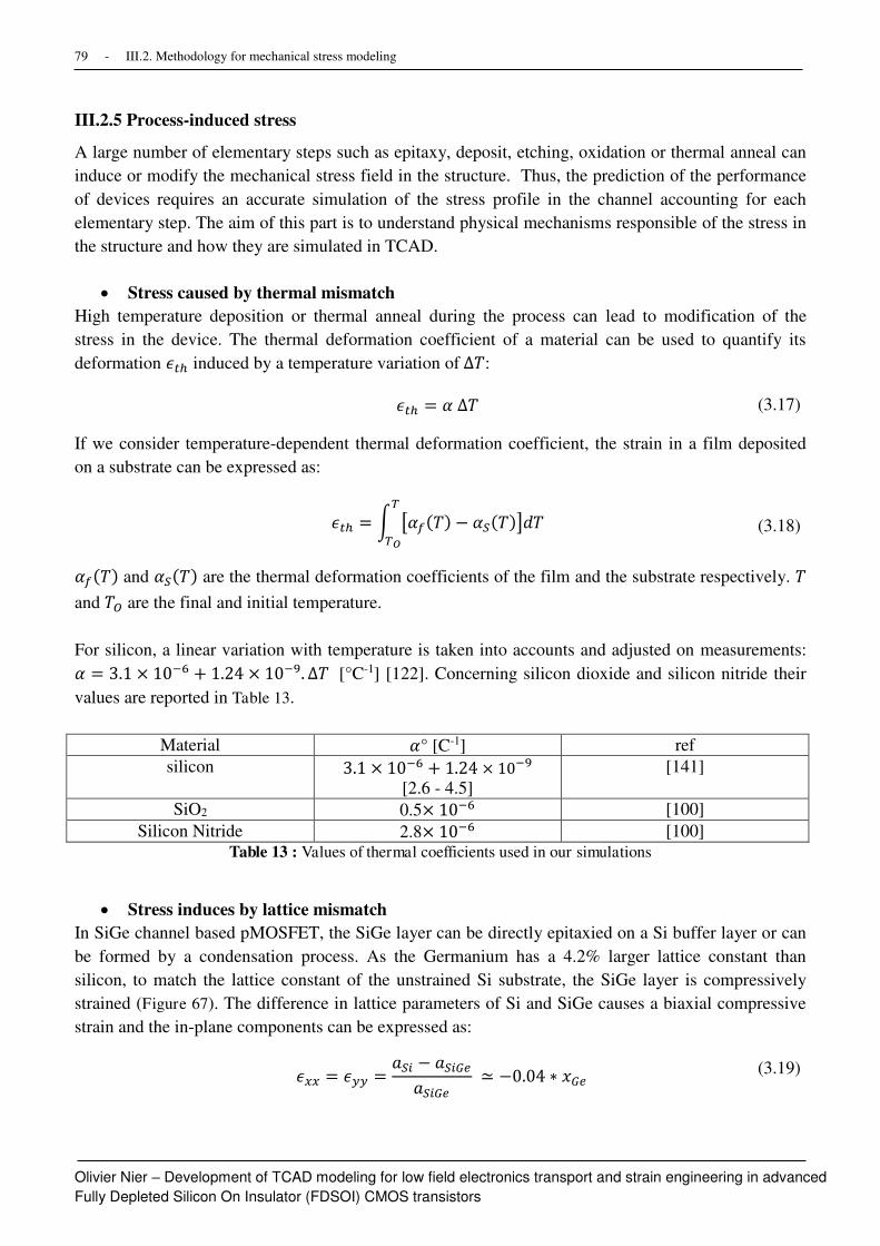
79 - III.2. Methodology for mechanical stress modeling
Olivier Nier – Development of TCAD modeling for low field electronics transport and strain engineering in advanced
Fully Depleted Silicon On Insulator (FDSOI) CMOS transistors
III.2.5 Process-induced stress
A large number of elementary steps such as epitaxy, deposit, etching, oxidation or thermal anneal can
induce or modify the mechanical stress field in the structure. Thus, the prediction of the performance
of devices requires an accurate simulation of the stress profile in the channel accounting for each
elementary step. The aim of this part is to understand physical mechanisms responsible of the stress in
the structure and how they are simulated in TCAD.
Stress caused by thermal mismatch
High temperature deposition or thermal anneal during the process can lead to modification of the
stress in the device. The thermal deformation coefficient of a material can be used to quantify its
deformation 香痛ℎ induced by a temperature variation of Δ劇:
香痛ℎ = � Δ劇 (3.17)
If we consider temperature-dependent thermal deformation coefficient, the strain in a film deposited
on a substrate can be expressed as:
香痛ℎ = ∫ [�捗岫劇岻 − �聴岫劇岻]穴劇脹脹� (3.18)
�捗岫劇岻 and �聴岫劇岻 are the thermal deformation coefficients of the film and the substrate respectively. 劇
and 劇潮 are the final and initial temperature.
For silicon, a linear variation with temperature is taken into accounts and adjusted on measurements: � = ぬ.な × など−滞 + な.にね × など−苔. Δ劇 [°C-1] [122]. Concerning silicon dioxide and silicon nitride their
values are reported in Table 13.
Material �° [C-1] ref
silicon ぬ.な × など−滞 + な.にね × など−苔 [2.6 - 4.5]
[141]
SiO2 0.5× など−滞 [100]
Silicon Nitride 2.8× など−滞 [100]
Table 13 : Values of thermal coefficients used in our simulations
Stress induces by lattice mismatch
In SiGe channel based pMOSFET, the SiGe layer can be directly epitaxied on a Si buffer layer or can
be formed by a condensation process. As the Germanium has a 4.2% larger lattice constant than
silicon, to match the lattice constant of the unstrained Si substrate, the SiGe layer is compressively
strained (Figure 67). The difference in lattice parameters of Si and SiGe causes a biaxial compressive
strain and the in-plane components can be expressed as:
香掴掴 = 香槻槻 = 欠聴沈 − 欠聴沈弔勅欠聴沈弔勅 ≃ −ど.どね ∗ 捲弔勅 (3.19)

80 - CHAPTER III. Mechanical simulations of the process-induced stress in 14FDSOI MOSFETs and comparison
with nanobeam diffraction strain measurements
Olivier Nier – Development of TCAD modeling for low field electronics transport and strain engineering in advanced
Fully Depleted Silicon On Insulator (FDSOI) CMOS transistors
The lattice constant in the growth direction is
香佃佃 = −に香掴掴系怠態/系怠怠 = −ど.ばば香掴掴 ≃ ど.どぬ ∗ 捲弔勅 (3.20)
And the strain tensor can be expressed as:
{ 香掴掴 = −ど.どね ∗ 捲弔勅香槻槻 = −ど.どね ∗ 捲弔勅香佃佃 = ど.どぬ ∗ 捲弔勅香掴槻 = ど香掴佃 = ど香槻佃 = ど
(3.21)
Figure 67 : (a) Schematic diagram of relaxed SiGe and silicon films. (b) Schematic diagram showing the lattice
distortion when the SiGe film is growth on top of the silicon film: the SiGe film is compressively strained.
Figure extracted from [140].
The SiGe channel for pMOS 14FDSOI technology (TEM cross-section shown in Figure 68) is formed
using the germanium condensation process. As, in TCAD, this step cannot be directly simulated, a
SiGe layer is deposited with a constant concentration of Germanium. We also assume that the level of
strain in the channel corresponds to the theoretical one (described by equation 3.21) so that no
relaxation has occurred during the condensation process. To validate these two hypotheses, an
Electron Dispersive X-Ray spectroscopy and a NBD analyses have been performed. The Electron
Dispersive X-Ray spectroscopy analysis along (Figure 69) the profile shown in Figure 68 highlights a
nearly uniform distribution of germanium in the channel (25% in that case). The NBD study (Figure
70) along the same profile shows a relative deformation in the SiGe channel of roughly zero in the
<110> direction. This indicates that the lattice parameter of the SiGe layer corresponds to the lattice
parameter of the reference (non-stressed silicon) so the SiGe layer is fully stressed (nearly 1.5 GPa in
this case). These two studies allow to validate the two simulation assumptions.

81 - III.2. Methodology for mechanical stress modeling
Olivier Nier – Development of TCAD modeling for low field electronics transport and strain engineering in advanced
Fully Depleted Silicon On Insulator (FDSOI) CMOS transistors
Figure 68 : TEM cross-section of the device after the formation of the SiGe channel by condensation. TEM
study performed by the team “physical characterization”.
Figure 69 : Electron Dispersive X-Ray (EDX) Spectroscopy analysis along the profile shown in Figure 68.
EDX analysis performed by the team “physical characterization”.
Figure 70 : Relative strain versus profile (shown in Figure 68) measured by NBD. NBD study performed by the
team “physical characterization”.

82 - CHAPTER III. Mechanical simulations of the process-induced stress in 14FDSOI MOSFETs and comparison
with nanobeam diffraction strain measurements
Olivier Nier – Development of TCAD modeling for low field electronics transport and strain engineering in advanced
Fully Depleted Silicon On Insulator (FDSOI) CMOS transistors
Material densification: STI example
High-density plasma (HDP) [107] [114] and high-aspect-ration process (HARP) [114] chemical vapor
deposition processes are the two main techniques to deposit STI oxides. For both techniques, the
deposited oxide is porous and a thermal heating is required to increase the density of the material. The
volume shrinkage of the STI during the heating directly generates stress in the devices. Moreover, for
14FDSOI technology devices, STI are deposited at 540°C using HARP CVD technique and a second
source of stress coming from the difference in CTE between the STI oxide and the substrate must be
considered. Measurements have been performed by depositing the oxide directly on the substrate on a
full wafer and a compressive stress of 220 MPa is measured in the STI layer. To take account for the
oxide densification during the thermal anneal, in TCAD, we have simulated the deposition of the
oxide on a full wafer (Figure 71). The stress induced by the difference in CTE between the STI oxide
and the substrate is approximately -150MPa and to match measurements, during the thermal anneal
(30min at 1050°C), a volume densification of 0.3% is added
Figure 71 : TCAD simulation of the deposition of the STI (540°C) on a full wafer.
III.3 Strain measurement techniques
Accurate determination of strain in electronic devices has been the subject of intense work during the
last decades. Techniques such as Raman [110] [111] [112] spectroscopy and X-Ray diffraction [113]
can be used for strain measurements but actual devices require a nanoscale resolution which can only
be obtained using transmission electron microscopy (TEM). TEM-based techniques can be divided
into two categories: diffraction-based techniques such as convergent-beam electron diffraction
(CBED) or nanobeam electron diffraction (NBD), and image-based techniques such as high-resolution
electron microscopy (HREM) or dark-field electron holography (HoloDark). The characteristics of
these techniques (e.g. the spatial resolution, the sensitivity …) are summarized in Table 14. It is
important to notice that the use of TEM-based techniques to measure the strain in FDSOI devices
require a thinning of the sample which is generally realized thanks to the focused ion beam (FIB) tool
[121]. One major difficulty with the thinning of the sample is to avoid the relaxation of the stress
during the preparation.

83 -
Olivier Nier – Development of TCAD modeling for low field electronics transport and strain engineering in advanced
Fully Depleted Silicon On Insulator (FDSOI) CMOS transistors
Strain
measurement
techniques
Spatial
resolution [nm]
Sensitivity Optimal thickness
of the sample [nm]
Characteristics References
High-Resolution
Electron
Microscopy
(HREM)
~ 2-3 1 × 10⁻³ ~ 50 - Mode: image
- Field of view :
image 150 * 150
nm²
- A close reference
(unstrained Si) is
required.
[115] [119]
Convergent-Beam
Electron
Diffraction
(CBED)
2 , 5, 1 2 × 10⁻⁴ > 300 -400 - Mode: probe [115] [120]
[116]
NanoBeam
electron
Diffraction (NBD)
5 , 2.7 6.0 × 10⁻⁴
1.0 × 10⁻³
~ 200 - Mode: probe [116] [119]
Dark-field
electron
holography
(HoloDark)
~ 4 2.5 × 10⁻⁴
2 × 10⁻⁴
~ 150 - Mode: image
- Field of view :
image 500 * 1500
nm²
- A close reference
(unstrained Si) is
required.
[115] [119]
Table 14 : Comparison of TEM-based strain measurement techniques.
During my thesis, strain measurements have been performed thanks to the NBD and the dark-field
electron holography techniques by the “physical characterization” team.
III.4 TCAD Stress-dependent mobility models.
Modeling of the mobility change with strain for drift diffusion device simulations usually falls into
two different categories of models. In the first one, analytical physics-based models have often been
developed for special stress configurations such as uniaxial longitudinal stress [117], biaxial stress
[118], or are restricted to silicon channel. The second category regroups mobility models such as the
linear and non-linear piezoresistive approach. The linear piezoresistive theory can be written as [123]:
Δ航賃鎮 = ∑Π賃鎮沈珍�沈珍沈珍 (3.22)
Where Δ航賃鎮 is the mobility variation, Π賃鎮沈珍 the piezoresistive tensor, �沈珍 the stress tensor and i,j,k,l the
coordinates. In crystals with cubic symmetry such as silicon, the number of independent coefficients
of the linear piezoresistance tensor reduces to three resulting in the following tensor for a (100)-
oriented channel (001) wafer (case where the crystallographic coordinate systems CCS coincide with
the device coordinate system CDS):
Π辿棚 = ( Π怠怠 Π怠態 Π怠態 ど ど どΠ怠態 Π怠怠 Π怠態 ど ど どΠ怠態 Π怠態 Π怠怠 ど ど どど ど ど Π替替 ど どど ど ど ど Π替替 どど ど ど ど ど Π滞滞)
(3.23)

84 - CHAPTER III. Mechanical simulations of the process-induced stress in 14FDSOI MOSFETs and comparison
with nanobeam diffraction strain measurements
Olivier Nier – Development of TCAD modeling for low field electronics transport and strain engineering in advanced
Fully Depleted Silicon On Insulator (FDSOI) CMOS transistors
For a (001)-oriented wafer device with a (110)-oriented channel, a rotation of 45° is applied around
the (001) axis leading to the following tensor:
Π辿棚 = ( Π宅 Π鐸 Π怠態 ど ど どΠ鐸 Π宅 Π怠態 ど ど どΠ怠態 Π怠態 Π怠怠 ど ど どど ど ど Π替替 ど どど ど ど ど Π替替 どど ど ど ど ど Π怠怠 − Π怠態)
(3.24)
Where Π宅 and Π鐸 are the longitudinal and transversal piezoresistance coefficients and are given by:
Π宅 = Π迭迭+Π迭鉄+Π44態 and Π鐸 = Π迭迭+Π迭鉄−Π44態 (3.25)
The bulk piezoresistive approach (equations 3.22) exploits silicon crystal symmetries to reduce the
piezoresistive tensor into four independent coefficients: Π怠怠, Π怠態 and Π替替 and Π滞滞 (equation 3.23 for a
(100)-oriented channel (001) wafer). As demonstrated in [127], this approach, despite the fact that it is
widely used in the electronic device community, is only valid at low stress values and in bulk silicon
crystal. Indeed, in silicon inversion layers, due to quantum confinement, the piezoresistive tensor
symmetries are reduced, and the number of independent coefficients increases up to six. The
piezoresistive tensor can now be written as:
Π辿棚 = ( Π怠怠 Π怠態 Π怠戴 ど ど どΠ怠態 Π怠怠 Π怠戴 ど ど どΠ怠戴 Π怠戴 Π戴戴 ど ど どど ど ど Π替替 ど どど ど ど ど Π替替 どど ど ど ど ど Π滞滞)
(3.26)
Moreover, as the inversion potential well is modulated by the normal electric field, piezoresistance
coefficients therefore depend on the effective electric field as mentioned in [127].
This latter behavior is clearly visible in Figure 72, where electron piezoresistance coefficients are
plotted versus effective field. At low effective field, 12 and 13 take approximately the same value,
as expected from the bulk theory. Moreover, the calculated 11, 12 and 13 are in good agreement
with the experimental results obtained in bulk silicon [123]. However, at higher effective field (i.e. Eeff
> 0.1 MV/cm), the piezoresistance coefficients differ from their bulk values. In particular, 12 and 13
are no longer equal, and can even change sign. This behavior can explain the large difference between
published coefficients for MOSFETs (Table 15), in particular for the coefficient 12. The holes
piezoresitance coefficients variations with the effective field are shown in Figure 73. A good
correlation is observed between simulation, data from literature and our simulations.

85 - III.4 TCAD Stress-dependent mobility models.
Olivier Nier – Development of TCAD modeling for low field electronics transport and strain engineering in advanced
Fully Depleted Silicon On Insulator (FDSOI) CMOS transistors
Figure 72 : nMOSFET piezo coefficients calculated using a KG solver and compared to literature. �岻 �層層, �層匝, �仔纂 �層惣 are obtained by applying a longitudinal, transversal and vertical stress on a <100> -
oriented channel MOSFET. �岻 �鯖 �仔纂 �参 are obtained by applying a longitudinal and transversal stress on
<110>-oriented channel MOSFET. Smith54: [123], Thompson06: [132], Weber07: [106].
Figure 73 : Same as Figure 72 but for pMOSFETs. PI1. Canali79: [125].
Piezoresistive
coefficients (×など−怠怠 Pa-1)
Bulk silicon Inversion layer
Electrons Holes Electrons Holes Π怠怠 -102.2
[123]
6.6
[123][126]
-42.6 [132]
-84 [125]
-38.6 [124]
Eeff=0.7MV/cm
Eeff=0.05MV/cm
Eeff=0.7MV/cm
9.1 [124]
-12.5 [125]
-1.0
Eeff=0.05MV/cm
Π怠態 53.4 [123] -1.1
[123][126]
-20.7
34 [125]
-18.7 [124]
Eeff=0.7MV/cm
Eeff=0.05MV/cm
Eeff=0.7MV/cm
-6.2 [124]
28.0 [125]
23.8 [126]
Eeff=0.05MV/cm
Π替替 -13.6 [123] 138.1
[123][126]
-21
-17 [125]
Eeff=0.7MV/cm
105.5 [124]
105.0 [125]
91.7
127.8 [126]
Eeff=0.05MV/cm
0 1 2 3 4 5 6 7 8 9 10
x 105
-100
-80
-60
-40
-20
0
20
40
60
80
100
Pie
zore
sis
tance c
oeff
icie
nts
valu
e (
x10-1
1)
Effective field (V/cm)
13
Smith54
Weber07
Thompson06
12
11
0 1 2 3 4 5 6 7 8 9 10
x 105
-40
-30
-20
-10
0
10
20
Pie
zore
sis
tance c
oeff
icie
nts
valu
e (
x10-1
1)
Effective field (V/cm)
L
T
Smith54
Thompson06 Weber07
0 1 2 3 4 5 6 7 8 9 10
x 105
-20
-10
0
10
20
30
40
50
60
Pie
zore
sis
tance c
oeff
icie
nts
valu
e (
x10-1
1)
Effective field (V/cm)
12
11
Weber07
Canali79
0 1 2 3 4 5 6 7 8 9 10
x 105
-80
-60
-40
-20
0
20
40
60
80
100
Effective field (V/cm)
Pie
zore
sis
tance c
oeff
icie
nts
valu
e (
x10-1
1)
L
Thompson06
T
Weber07Smith54

86 - CHAPTER III. Mechanical simulations of the process-induced stress in 14FDSOI MOSFETs and comparison
with nanobeam diffraction strain measurements
Olivier Nier – Development of TCAD modeling for low field electronics transport and strain engineering in advanced
Fully Depleted Silicon On Insulator (FDSOI) CMOS transistors
Piezoresistive coefficients (×など−怠怠 Pa-1)
Bulk silicon Inversion layer
Electrons Holes Electrons Holes Π挑 -31.2 [123]
-26.0 [131]
71.8 [123]
53.5 [131]
-35.5 [132][124]
-48.5 [133]
-31.5 [134]
-30.0 [135]
Eeff=0.7MV/cm
71.7
[132][124]
60 [133]
71.8 [134]
59.0 [134]
Π脹 -17.6 [123]
-12 [131]
-66.3 [123]
-58.5 [131]
-14.5 [132][124]
-21.2 [133]
Eeff=0.7MV/cm
-33.8
[132][124]
-38.3 [133]
Table 15 : Piezoresistive coefficients values for bulk silicon and in the case of an inversion layer.
Piezoresistance coefficients measurement
The piezoresistance coefficients have been extracted using the 4 points wafer bending technique on
28FDSOI technology devices. Figure 74 shows the 4 points the bender used for piezoresistive
coefficients measurements.
Figure 74 : Picture (a) and schematic diagram (b) of the 4 points the bender used for piezoresistive coefficients
measurements
The curvature radius of the strip is measured thanks to a CCD camera and linked to the uniaxial stress
thanks to the expression
� = − 結継に迎 (3.27)
with 継 the Young modulus (継<怠怠待> = なはぱ 罫鶏欠, 継<怠待待> = なにぱ 罫鶏欠 ), 結 the strip thickness and 迎 the
curvature radius. A uniaxial stress ranging from -150 MPa to 150 MPa is applied to the strip thanks to
the bender and the mobility variation is measured at VG=1.5V Figure 75a, and Figure 75b show the
measured mobility variation as a function of the applied stress for n-type (a) <100>-oriented and b)
<110>-oriented channel and p-type MOSFET (Figure 76). The extracted coefficients are listed in Table
16 and are similar to coefficients found in literature (Table 15).

87 - III.4 TCAD Stress-dependent mobility models.
Olivier Nier – Development of TCAD modeling for low field electronics transport and strain engineering in advanced
Fully Depleted Silicon On Insulator (FDSOI) CMOS transistors
Figure 75 : Mobility variation with stress for a) <100>-oriented and b) <110>-oriented channel nFDSOI
devices. The extracted piezoresistance coefficients are listed in Table 16. Measurements are performed on
28FDSOI technology (device described in part II.3).
Figure 76 : Mobility variation with stress for <110>-oriented channel pFDSOI devices. The extracted
piezoresistance coefficients are listed in Table 16.
NMOS PMOS
Channel <110> Channel <110>
Stress Direction Piezo Coeff [Pa-1] Stress Direction Piezo Coeff [Pa-1]
<110> -49e-11 <110>
<-110> -22e-11 <-110> -50e-11
<001> -24e-11 <001>
Channel <100> Channel <100>
<100> -55e-11 <100> Low value
<010> -18e-11 <010> Low value
Table 16 : Piezoresistance coefficients extracted from wafer bending measurements
-150 -100 -50 0 50 100 1500.9
0.95
1
1.05
1.1
STRESS [MPa]
MO
BIL
ITY
VA
RIA
TIO
N
<100>-oriented channel
<010>:-18e-11
<100>:-55e-11
-150 -100 -50 0 50 100 1500.92
0.94
0.96
0.98
1
1.02
1.04
STRESS [MPa]
MO
BIL
ITY
VA
RIA
TIO
N
<110>-oriented channel
<110>: -49e-11 Pa-1
<001>: -24e-11 Pa-1
<-110>: -22e-11 Pa-1
-150 -100 -50 0 50 100 1500.92
0.94
0.96
0.98
1
1.02
1.04
1.06<110>-oriented channel
STRESS [MPa]
MO
BIL
ITY
VA
RIA
TIO
N
<-110>: -50e-11 Pa-1
<110>

88 - CHAPTER III. Mechanical simulations of the process-induced stress in 14FDSOI MOSFETs and comparison
with nanobeam diffraction strain measurements
Olivier Nier – Development of TCAD modeling for low field electronics transport and strain engineering in advanced
Fully Depleted Silicon On Insulator (FDSOI) CMOS transistors
Validity of the piezoresistive theory:
The linear piezoresistive theory is valid only in a limited range of stress as already highlighted in
[127]. Indeed, for high stress values (> 300 MPa), the mobility variation can exhibit a large nonlinear
dependence with stress. In Figure 77, a linear and an exponential piezo model is compared to KG
calculations applying a longitudinal uniaxial stress on a <110>-oriented channel device. In that case,
we can notice that these two models are not able to reproduce the mobility variation for stress up to
300 MPa.
Figure 77 : Hole mobility variation (extracted at Eeff=1 MV/cm) in <110>-oriented silicon channel pMOSFETs
as a function of the longitudinal uniaxial stress (stress applied in the <110> direction).
Linear model: �侍/侍 = −�鯖 × �. Exponential model: �侍/侍 = 蚕�使 岫−�鯖 × �岻 with �鯖 = 挿挿 ×層宋−層層 ��−層
The linear piezoresistive theory has been widely used to evaluate the mobility variation with stress.
However, in actual UTBB-FDSOI devices, the stress can reach values between -1 and -2 GPa and the
linear piezoresistive theory is no longer valid. In the next section we present a TCAD mobility model
which extends the piezoresistive approach.
Stress-dependent mobility model in TCAD: MCmob:
MCmob is a stress-dependent mobility model for the commercial device simulator Sentaurus Device
by Synopsys which extends the piezoresistive approach validity in the high stress range [100] [127].
The variation of mobility with stress is given by the two following models:
Δμμ頂 =∑欠珍,聴沈弔勅,懲,挑,沈,達. �珍沈滞沈=怠 (3.28)
Δμμ頂 = 欠珍,聴沈弔勅,懲,挑,怠,達結銚乳,縄日奈賑,凪,薙,鉄,冬∗�乳 + 欠珍,聴沈弔勅,懲,挑,戴,達結銚乳,縄日奈賑,凪,薙,4,冬∗�乳 欠珍,聴沈弔勅,懲,挑,泰,達結銚乳,縄日奈賑,凪,薙,鉄,冬∗�乳 + 欠珍,聴沈弔勅,懲,挑,滞,達結銚乳,縄日奈賑,凪,薙,4,冬∗�乳 (3.29)
-2000 -1500 -1000 -500 0
0
50
100
150
200
250
300
350
400
Uniaxial Stress (MPa)
Mo
bility v
ari
atio
n (
%)
Linar Piezo Model
Exponential Piezo Model
Kubo Greenwood

89 - III.4 TCAD Stress-dependent mobility models.
Olivier Nier – Development of TCAD modeling for low field electronics transport and strain engineering in advanced
Fully Depleted Silicon On Insulator (FDSOI) CMOS transistors
where j refers to the direction of the applied stress (c: channel, w: width or n: normal), SiGe is the
germanium mole fraction, K and L are the wafer and channel orientations and i is the index of the
coefficients c is the carrier type (h for holes and e for electrons)
The implemented expression (equations 3.28 or 3.29) depends on the carrier type (electrons or holes),
the channel orientation (100 or 110) and the direction of the applied stress (c: channel, w: width and n:
normal). Expressions for each condition are summarized in Table 17.
Holes Electrons
<100> Channel <110> Channel <100> Channel <110> Channel
Stress orientation
(100) c / (010) w /
(001) n
Stress orientation
(110) c / (-110) w
/ (001) n
Stress orientation
(010) w
Stress orientation
(110) c / (-110) w Eq. 3.28
Stress orientation
(100) c / (001) n
Stress orientation
(001) n Eq. 3.29
Table 17 : MCmob model description for uniaxial stress.
In order to improve interpolation in some specific stress conditions, e.g. biaxial stress, a cross terms correction is introduced:
Δμμ頂 = (Δμμ頂 )醍単.戴.態腿 誰嘆 戴.態苔 + 系岫�堅岻 (3.30)
The cross terms correction 系岫�追岻 is the sum of nineteen coefficients multiplied by different combinations of uniaxial stress components �堅. Such coefficients and their coupling stress components are listed in Table 18 in the case of a (K)-oriented wafer device with a <L>-oriented channel.
Coefficients Coupling
stress comp. Coefficients
Coupling Stress comp.
asKcL1h σc*σn asKcL11h σc*σw*σw*σw asKcL2h σc*σw asKcL12h σc*σn*σn*σn asKcL3h σn*σw asKcL13h σn*σc*σc*σc asKcL4h σc*σw*σw asKcL14h σn*σw*σw*σw asKcL5h σc*σn*σn asKcL15h σw*σc*σc*σc asKcL6h σn*σc*σc asKcL16h σw*σn*σn*σn asKcL7h σn*σw*σw asKcL17h σn*σn*σw*σw asKcL8h σw*σc*σc asKcL18h σc*σc*σw*σw asKcL9h σw*σn*σn asKcL19h σc*σc*σn*σn asKcL10h σc*σn*σw
Table 18 : MCmob cross terms correction coefficients
The calibration of MCmob is performed using a Sband KG solver as a reference. The effective mobility
variation with stress is calculated for three uniaxial and three biaxial conditions. MCmob model
parameters have been determined using a mixed global-to-local optimization strategy to ensure accurate
and robust solutions. Indeed, the large number of coefficients for each orientation can leads to complex
structures of error minima. As a first step, a global parameter optimization, using DIRECT algorithm
[128], is performed. Afterwards, a local optimization procedure is applied to increase the accuracy of
the fit. Figure 78 and Figure 79 show good agreements between mobility variations calculated with
MCmob and UTOXPP at Eeff=1 MV/cm for holes and electrons respectively. The major limitation of
MCmob model is the non-dependence of the mobility variation with the effective field.
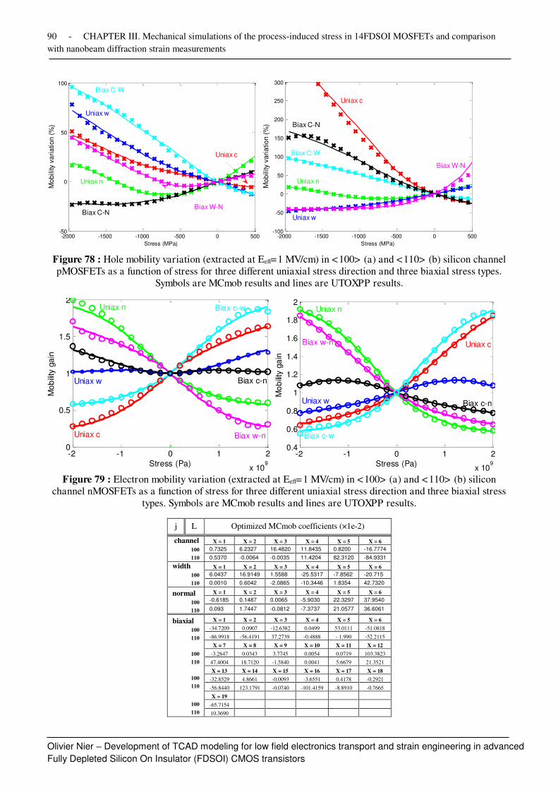
90 - CHAPTER III. Mechanical simulations of the process-induced stress in 14FDSOI MOSFETs and comparison
with nanobeam diffraction strain measurements
Olivier Nier – Development of TCAD modeling for low field electronics transport and strain engineering in advanced
Fully Depleted Silicon On Insulator (FDSOI) CMOS transistors
Figure 78 : Hole mobility variation (extracted at Eeff=1 MV/cm) in <100> (a) and <110> (b) silicon channel
pMOSFETs as a function of stress for three different uniaxial stress direction and three biaxial stress types.
Symbols are MCmob results and lines are UTOXPP results.
Figure 79 : Electron mobility variation (extracted at Eeff=1 MV/cm) in <100> (a) and <110> (b) silicon
channel nMOSFETs as a function of stress for three different uniaxial stress direction and three biaxial stress
types. Symbols are MCmob results and lines are UTOXPP results.
j L Optimized MCmob coefficients (×1e-2)
channel
100
110
X = 1 X = 2 X = 3 X = 4 X = 5 X = 6 0.7325 6.2327 16.4820 11.8435 0.8200 -16.7774
0.5370 -0.0064 -0.0035 11.4204 82.3120 -84.9331
width
100
110
X = 1 X = 2 X = 3 X = 4 X = 5 X = 6 6.0437 16.9149 1.5588 -25.5317 -7.8562 -20.715
0.0010 0.6042 -2.0865 -10.3446 1.8354 42.7320
normal
100
110
X = 1 X = 2 X = 3 X = 4 X = 5 X = 6 -0.6185 0.1487 0.0065 -5.9030 22.3297 37.9540
0.093 1.7447 -0.0812 -7.3737 21.0577 36.6061
biaxial 100
110
100
110
100
110
100
110
X = 1 X = 2 X = 3 X = 4 X = 5 X = 6 -34.7209 0.0907 -12.6382 0.0499 53.0111 -51.0818
-86.9918 -56.4191 37.2739 -0.4888 - 1.990 -52.2115
X = 7 X = 8 X = 9 X = 10 X = 11 X = 12 -3.2647 0.0343 3.7745 0.0054 0.0719 103.3823
47.4004 18.7120 -1.5840 0.0041 5.6679 21.3521
X = 13 X = 14 X = 15 X = 16 X = 17 X = 18 -32.8529 4.8661 -0.0093 -3.6551 0.4178 -0.2921
-56.8440 123.1791 -0.0740 -101.4159 -8.8910 -0.7665
X = 19
-65.7154
10.3690
-2000 -1500 -1000 -500 0 500-50
0
50
100
Mo
bility v
ari
atio
n (
%)
Stress (MPa)
Biax C-W
Uniax w
Uniax c
Biax W-N
Uniax n
Biax C-N
-2000 -1500 -1000 -500 0 500-100
-50
0
50
100
150
200
250
300
Stress (MPa)
Mo
bility v
ari
atio
n (
%)
Biax C-W
Uniax w
Uniax c
Biax W-N
Uniax n
Biax C-N
-2 -1 0 1 2
x 109
0
0.5
1
1.5
2
Stress (Pa)
Mo
bili
ty g
ain
Biax c-w
Uniax c
Uniax n
Uniax w Biax c-n
Biax w-n
-2 -1 0 1 2
x 109
0.4
0.6
0.8
1
1.2
1.4
1.6
1.8
2
Mo
bili
ty g
ain
Stress (Pa)
Biax c-w
Uniax c
Uniax n
Uniax w Biax c-n
Biax w-n

91 - III.5 Conclusion
Olivier Nier – Development of TCAD modeling for low field electronics transport and strain engineering in advanced
Fully Depleted Silicon On Insulator (FDSOI) CMOS transistors
Table 19 : Calibrated MCmob parameters for holes
j L Optimized MCmob coefficients (×1e-2)
channel
100
110
X = 1 X = 2 X = 3 X = 4 X = 5 X = 6 0.0119 8.8275 -0.0119 10.1496 -0.0142 -0.0162
-0.0023 0.0009 0.0009 -0.0154 0.0949 0.3489
width
100
110
X = 1 X = 2 X = 3 X = 4 X = 5 X = 6 0.0021 -0.0061 -0.0221 0.0441 0.0965 -0.0042
0.0000 0.0037 -0.0049 -0.0381 0.0006 0.1702
normal
100
110
X = 1 X = 2 X = 3 X = 4 X = 5 X = 6 -0.0059 0.8026 0.0059 -0.8654 0.0140 0.0052
0.0002 0.5980 -0.0002 -1.1025 -0.0004 -0.0002
biaxial 100
110
100
110
100
110
100
110
X = 1 X = 2 X = 3 X = 4 X = 5 X = 6 -0.0706 0.0965 -0.3270 -0.6064 0.9640 -0.9834
-0.2498 0.0457 -0.0240 -0.0297 0.0275 -0.0384
X = 7 X = 8 X = 9 X = 10 X = 11 X = 12 1.8577 0.5813 -1.8763 4.0001 2.0618 0.5179
-0.0227 0.0174 0.0123 5.1177 -0.0533 0.0243
X = 13 X = 14 X = 15 X = 16 X = 17 X = 18 -1.5491 -2.7978 -1.9867 0.0314 2.8193 -0.0941
0.0030 0.0043 0.0044 0.0066 0.0000 0.0400
X = 19
1.0447
0.0000
Table 20 : Calibrated MCmob parameters for electrons.
III.5 Conclusion
In the first part of this chapter, a review of the methodologies used during my thesis to model
the mechanical stress in FDSOI structure is performed. After recalling some generalities about
stress/strain tensors and simulations boundary conditions, a description of the widely encountered
materials rheological behaviors is performed, namely elastic, viscoelastic and plastic laws. Then, the
physical mechanisms responsible of the stress in the structure and their methodology of simulation are
studied. We focused on the description of the main technology boosters to induce stress in 28 and 14
FDSOI technologies such as SiGe channel, SiGe source and drain, STI … The second part of this
chapter has been dedicated to the description of strain measurements methods. During this thesis,
strain has been measured thanks to nanobeam electron diffraction and the dark-field electron
holography techniques. These two techniques have been used as references to validate our simulations
(Chapter III and IV). Then, in the last part, we presented an accurate description, study and calibration
of a TCAD stress-dependent mobility models (MCmob). Finally, in this chapter, we set up the
methodology for process-induced stress simulations and to calculate its influence on electrical
characteristics. This enables accurate and efficient TCAD simulations of strained-Si FDSOI
MOSFETs in state of the art CMOS technology. The application of these methods to optimize
STMicroelectronics devices is the topic of the fourth chapter.

92
Chapter IV:
ST-oriented device applications
IV.1 Introduction ................................................................................................................................................ 93
IV.2. Process flow description for 14FDSOI technology ................................................................................. 93
IV.3 28FDSOI/14FDSOI mechanical stress study ........................................................................................... 94
IV.3.1 STI process steps and layout effects. ..................................................................................................... 94
IV.3.2 Stress relaxation during STI process steps: NBD Strain measurements................................................ 97
IV.3.3 TCAD calibration on NBD measurements ............................................................................................ 99
IV.4.3 SiGe Source and Drain ........................................................................................................................ 104
IV.4 Stress state optimization for 14FDSOI devices. ..................................................................................... 107
IV.4.1 Introduction of a piezoelectric layer .................................................................................................... 107
IV.4.2 Stress configuration optimization for n- and p-type MOSFETs. ......................................................... 108
IV.5 Conclusion ................................................................................................................................................. 113

93 - IV.1 Introduction
Olivier Nier – Development of TCAD modeling for low field electronics transport and strain engineering in advanced
Fully Depleted Silicon On Insulator (FDSOI) CMOS transistors
IV.1 Introduction
FDSOI technology is considered as one of the best solution to keep increasing CMOS performances
while scaling device dimensions, especially for low power applications [69] [70]. However the use of
stress engineering to enhance electrons and holes transport properties is mandatory to reach ITRS [1]
requirements for the 14 nm node and beyond. This is more critical in the case of advanced FDSOI
technology, as high-k metal gate stacks [71] [72] and scattering with back interface [34] [46] both
contribute to further degrade transport, as seen previously in chapter II. Moreover, in case of SiGe-
based FDSOI devices, due to the specific mechanical properties of the ultra-thin active layer and the
Buried Oxide (BOX), the solutions developed to strain bulk devices have to be reinvestigated. The
development of 28 and 14FDSOI technologies requires accurate TCAD modeling of the stress profile
in the transistor and its impact on the electrical performances (using for instance the approach
described in chapter III). Consequently, a TCAD methodology to model the process flow has been
developed during this thesis, specifically for the modeling of 14FDSOI and 10FDSOI technologies
and aiming at supporting technology developments. The aim of this chapter is twofold. In the first
place, mechanical simulations are performed to model the stress profile in 14FDSOI transistors
(methodologies described in chapter III). A particular attention has been paid to the modeling of stress
relaxation during STI process steps and to the impact of SiGe source and drain. In the second place,
some electrical characteristics of these devices have been investigated more closely.
In the first part of this chapter, we perform a brief description of the developed TCAD approach to
model 14/10FDSOI technology. Then, in the second part, a full mechanical study of the stress
configuration in 14FDSOI technology has been performed through TCAD simulations and NBD
measurements. Solutions to optimize the stress configuration in sSOI and SiGe-based devices are
proposed. Finally, 14FDOI MOSFETs electrical performances have been investigated in more details
IV.2. Process flow description for 14FDSOI technology
The main process steps of 14FDSOI technology are listed in Figure 80 and the whole flow has been
simulated using Sprocess (SYNOPSYS) tool. 14FDSOI devices are processed on 300 mm SOI wafers
with a 25 nm thick BOX. The oxide stack is made of a 1.8 nm thick layer of high-k oxide (HfSiON)
deposited on top of an SiON interfacial layer (IL) with various EOT from 0.7 to 3.0 nm The final
silicon channel thickness is 7.0 nm and the p-type devices feature SiGe (xGe=22%) channel and source
and drain (xGe=30%). Simulations are calibrated on TEM images to accurately reproduce the device
topography (as shown in Figure 47).
Figure 80 : Simplified description of the process flow for 14FDSOI technology.

94 - CHAPTER IV. ST-oriented device applications
Olivier Nier – Development of TCAD modeling for low field electronics transport and strain engineering in advanced
Fully Depleted Silicon On Insulator (FDSOI) CMOS transistors
In Figure 81, the result of TCAD process simulation of a p-type device is shown after STI isolation
steps, gate stack deposition, spacer formation and SiGe S&D. It is important to notice that main steps
leading to mechanical stress in p-type devices are: the SiGe channel formation, the SiGe source and
drain and the high temperature material deposition (STI, Gate stack). Other sources of stress can come
from contact silicidation but are not considered in our simulations.
Figure 81 : TCAD process simulation of 14FDSOI technology after a) STI isolation steps, b) Gate
stack deposition, c) spacer formation and d) SiGe S&D epitaxy.
Combining the methodologies described in chapter III and the accurate modeling of the process flow,
mechanical stress studies can be performed, and are presented below.
IV.3 28FDSOI/14FDSOI mechanical stress study
As previously explained, global stress techniques such as strained SiGe channel or “strained Silicon On Insulator” (sSOI) [105], are current techniques to enhance carriers mobilities in MOSFETs. The
resulting compressive or tensile biaxial stress is introduced into the whole wafer at the beginning of
the process flow, it can undergo however several modifications during etching, deposition or thermal
heating process steps. This part aims at studying the stress configuration and its evolution during the
different process steps. It accounts for the main sources of stress for pMOSFETs, namely, strained
SiGe channel, SiGe source and drain, STI and gate stack deposition. Simulations are compared to
NBD strain measurements, and several simulations have been performed to optimize the stress
configuration in the channel.
IV.3.1 STI process steps and layout effects.
The STI deposition requires several process steps (Figure 82) which are presented schematically in
Figure 83. First of all, a hard mask is deposited on the surfaces that must be protected from etching.
Then, the etching step allows to form the shape of the STI. Note that in this example, the two STI are
dissymmetric, and are referred as shallow and deep STI. The STI is deposited at high temperature
thanks to HDP [109] [114] or HARP [114] chemical vapor deposition techniques and a thermal anneal
allows to make the STI denser. The simulations of the two last steps are described in part III.2.
Finally, the hard mask is removed.
a) b)
c) d)

95 - IV.3 28FDSOI/14FDSOI mechanical stress study
Olivier Nier – Development of TCAD modeling for low field electronics transport and strain engineering in advanced
Fully Depleted Silicon On Insulator (FDSOI) CMOS transistors
Figure 82 : STI process flow for 28/14 FDSOI technology.
.
Figure 83 : Schematic description of the STI process steps. It can be noticed that a dual STI (deep and shallow
STI) has been analyzed.
The evolution of the stress profile along the channel direction is shown in Figure 84. Initially the active
layer is compressively stressed to 1.5 GPa, thanks to the use of an SiGe channel with xGe=22%. A
first relaxation occurs due to the STI etch (step 1), reducing the stress to the value of 1.3 GPa at the
center of the channel. This value further decreases close to the edge of the channel and is null at each
sides (free surfaces). Represented by the step 2, the high temperature deposition of the STI adds a
compressive stress in the channel due to the difference of CTE between oxide and silicon. During the
STI anneal, a second important stress relaxation occurs, leading to a value of 800 MPa at the center of
the channel. The high temperature anneal has indeed induced a decrease of the viscosity of the oxides
and nitrides layers, facilitating the stress relaxation within the channel. However it is important to
notice that this stress relaxation depends strongly on the value of the oxide viscosity (taken from
[137]) which is not known with accuracy. Indeed, this property is significantly dependent on the oxide
type, the temperature and composition (impurity). So a quantitative estimation of the contribution of
both STI etch and STI anneal stress relaxations remains difficult in absence of calibration on
measurements. Finally, the hard mask removal has not been found to impact significantly the stress
profile in the channel.

96 - CHAPTER IV. ST-oriented device applications
Olivier Nier – Development of TCAD modeling for low field electronics transport and strain engineering in advanced
Fully Depleted Silicon On Insulator (FDSOI) CMOS transistors
Figure 84 : Evolution of the stress profile along the channel direction during STI process steps. Numbers in in
the figure corresponds to process steps described in Figure 83.
The process previously described is something called the “SiGe first” approach, as the SiGe channel is
formed by condensation, before STI process steps. An alternative solution would consist in performing
the condensation steps after the STI (“SiGe last”). This solution is expected to reduce the stress
relaxation due to the STI etching. We have evaluated the stress profile in the channel resulting from
these two methods (Figure 85). A strong reduction of the stress relaxation is indeed observed with the
SiGe last method (σL = -1.35 GPa) compared to SiGe first (σL = -0.8 GPa).
Figure 85 : Simulation of the evolution of the stress profile along the channel direction. Two cases have been
considerate: SiGe first and SiGe last. Lactive=130 nm.
Stress dependence on layout dimensions: a difficult compromise between Lactive and
Wactive effects.
The relaxation of the SiGe channel stress during the STI process steps leads to “layout effects”, which
means that the mean longitudinal stress (σL) and transversal stress (σW) in the channel depend on the
active layer dimensions namely Lactive and Wactive (as previously introduced in chapter III). Indeed, as
shown in Figure 86a, a strong decrease of the mean longitudinal stress in the channel is observed for
decreasing active length. Similarly, the mean transversal stress decreases with the active width. The
difference between the two trends are simply due to the fact that the stress is averaged on the channel
length for σL and over the whole width for σW. The resulting simulated channel mobility variations
with the active length and width are shown in Figure 86b. Two different trends have been found: the
reduction of Lactive dimension induces a mobility reduction in the channel while the reduced of Wactive
leads to a mobility increase. Indeed, when the transversal compressive stress σW is relaxed, the
channel mobility is enhanced. This highlights the fact that p-type devices are stressed in a non-optimal

97 - IV.3 28FDSOI/14FDSOI mechanical stress study
Olivier Nier – Development of TCAD modeling for low field electronics transport and strain engineering in advanced
Fully Depleted Silicon On Insulator (FDSOI) CMOS transistors
way. To explain this behavior, the hole mobility variation with stress is shown for a (110)-oriented
channel in Figure 87 on which three different stress configurations are represented: i) longitudinal
uniaxial, ii) transversal uniaxial and iii) biaxial. We can notice that a longitudinal uniaxial stress
improves the mobility much more than a biaxial stress, and that the relaxation of the transversal stress
is favorable for p-type MOSFET performances.
Figure 86 : Left) Simulated mean longitudinal stress (average on the channel region) with Lactive and the mean
transversal stress (average on the whole width) with Wactive. Right) Simulated hole mobility variation with Lactive
and Wactive using KG solver (channel wafer)
Figure 87 : Simulated (KG solver) hole mobility variation (extracted at Eeff=1 MV/cm) in a) <100> and b)
silicon channel pMOSFETs as a function of stress.
Actually, there is no differentiation between process steps forming the isolation trenches in L en W
directions. Consequently the stress configuration in these directions are correlated and depends
exclusively on the dimensions of the active layer (Lactive for longitudinal stress and Wactive for
transversal stress). Propositions to optimize the stress configuration in the device are discussed in
section IV.4.2.
These results are based on TCAD simulations and require a validation with experimental data.
IV.3.2 Stress relaxation during STI process steps: NBD Strain measurements.
The stress profile after STI process steps have been measured using the NBD technique on the TEM
structure shown in Figure 88.
0 0.5 1 1.5-15
-10
-5
0x 10
8
Str
ess
(P
a)
Lactive
or Wactive
L
W
0 0.5 1 1.50
0.5
1
1.5
2
2.5
Lactive
or Wactive
MO
BIL
ITY
VA
RIA
TIO
N
mobility (Wact)
mobility (Lact)
-2000 -1500 -1000 -500 0 500-100
-50
0
50
100
150
200
250
300
Stress (MPa)
Mob
ility v
ari
atio
n(%
)
Silicon channel <110>
Transversal uniaxial
Longitudinal uniaxial
Biaxial

98 - CHAPTER IV. ST-oriented device applications
Olivier Nier – Development of TCAD modeling for low field electronics transport and strain engineering in advanced
Fully Depleted Silicon On Insulator (FDSOI) CMOS transistors
Figure 88 : TEM picture of the studied device. Measurements are performed after STI formation steps. The
dotted line corresponds to the profile where NBD measurements have been performed.
Figure 89 : Measurements of the deformation profile (εxx and εyy) thanks to NBD measurements. Profile shown
in Figure 88. xGe = 22%. Measurements have been performed before STI anneal.
Figure 90 : Measurements of the deformation profile εxx
The longitudinal deformation εxx profile has been measured after four different steps (Figure 90): i)
after “MESA” etching (corresponding to a deep etching), ii) after “STI” etching, iii) before STI anneal and iiii) after STI anneal. Initially, after Ge condensation process step, the lattice constant of the SiGe
layer should match the one of the silicon reference, so the relative deformation should be null in
-0,5%
0,0%
0,5%
1,0%
1,5%
0 100 200 300 400 500
Def
orm
atio
n
Profile [nm]
Exx
Eyy
-0,5%
0,0%
0,5%
1,0%
1,5%
0 100 200 300 400 500
Def
orm
atio
n
Profile [nm]
Exx-GravureMESA-TBOX
Exx-GravureSTI-TBOX
Exx-BeforeSTIAnnea-TBOX
Exx-AfterSTIAnneal-TBOX
0 nm

99 - IV.3 28FDSOI/14FDSOI mechanical stress study
Olivier Nier – Development of TCAD modeling for low field electronics transport and strain engineering in advanced
Fully Depleted Silicon On Insulator (FDSOI) CMOS transistors
principle all along the profile. A first relaxation occurs due to the STI etch (also observed in Figure
89). The relative deformation is still null for distances up to 500 nm and increases close to the edge of
the channel. This corresponds to a relaxation of the strain near the STI interface. Note that no
significant difference has been found between the two etching types (MESA and STI). Then, the high
temperature deposition adds a compressive strain in the channel, as previously shown in TCAD
simulation (part IV.3.1). The last measurement is performed after STI anneal, and no significant
influence of this step has been observed. This observation suggests that in the TCAD simulations, the
relaxation of the longitudinal stress due to STI anneal has been overestimated (for this corresponding
anneal temperature -1050°C-). Simulations and experiments are compared more accurately in the
following part.
IV.3.3 TCAD calibration on NBD measurements
In Figure 91, NBD measurements after STI patterning have been compared to TCAD simulations. We
can notice that the important relaxation of the SiGe film observed after STI patterning by NBD
measurements (represented as points in the figure) can not be explained by a simple elastic theory
used in the simulation (full red curve). Another phenomenon degrades the stress and is probably
linked to the SiGe / BOX interface. Indeed, we suspect that the bonding between the SiGe layer and
the BOX surface is weak and cannot hold the stress in the channel during STI patterning. As this
phenomenon is not included in the simulation, artificial relaxations have been introduced in TCAD by
adding additional anneal steps (dotted lines).
Figure 91 : Relative longitudinal deformation εxx measured by NBD, and comparison to TCAD simulations.
NBD measurements have then been performed after STI patterning and at the end of the process flow
on structure presented in Figure 92. This structure is an interdigited PMOS with a large active length
featuring a SiGe channel (xGe=22%) and source and drain (30%).
Figure 92 : TEM pictures of the simulated structure. The dotted line corresponds to the profile where NBD
measurements have been performed.
0 nm
Profile [nm]

100 - CHAPTER IV. ST-oriented device applications
Olivier Nier – Development of TCAD modeling for low field electronics transport and strain engineering in advanced
Fully Depleted Silicon On Insulator (FDSOI) CMOS transistors
Figure 93 shows that, after STI patterning, the relative deformation is null for distances up to 500 nm
indicating a fully stressed SiGe channel. Moreover, close to the edge of the channel, the relative
deformation increases, indicating a relaxation of the strain (close to the STI edge). This behavior has
already been observed in Figure 90. Concerning NBD measurements on the fully processed device, the
relative deformation exhibits an oscillating behavior which is due to the presence of embedded SiGe
sources and drains and gate stacks. Quite good agreement is found between TCAD simulation and
NBD measurements.
Figure 93 : Comparison between TCAD simulations and NBD measurements of the deformation profile εxx post
STI patterning and at the end of the process. Device of Figure 92.
The dependence of the normalized (reference: long SA/SB) drain current (Iodlin corresponds to the
drain current at VG=VTH - 0.5V) as a function of SA/SB (Lactive = SA + Lch + SB; dimensions shown in
Figure 94b) and compared to TCAD simulations. As previously observed in simulations, the decreases
of the active length causes a relaxation of the longitudinal stress leading to a reduction of the mobility.
Consequently, p-type performance (Iodlin in that case) are degraded for small SA/SB (~50%). Good
agreement are found between TCAD and NBD measurements. Note that the variation of the width has
a limited influence on Iodlin (SA/SB) characteristics. In Figure 95, the Iodlin variation is plotted as a
function of the active width Wactive. As previously observed in simulations, the decreases of the active
width causes a relaxation of the transversal stress leading to an enhancement of the mobility.
Consequently, p-type performance are improved for small SA/SB (~20%).

101 - Extraction of the relaxation length from measurements
Olivier Nier – Development of TCAD modeling for low field electronics transport and strain engineering in advanced
Fully Depleted Silicon On Insulator (FDSOI) CMOS transistors
Figure 94 : Left: Definition of the notation SA and SB. Right: comparison between measured relative Iodlin
variation (reference: long SA/SB) and TCAD simulations as a function of SA/SB
Figure 95 : Comparison between measured relative Iodlin variation (reference: long SA/SB) and TCAD
simulations as a function of W.
Extraction of the relaxation length from measurements
The aim of this study is to extract a characteristic strain relaxation length from current measurements.
It consists in reducing the information contained in the current vs active length variation to a numeric
characteristic distance. Two methods can be used: i) a direct extraction method where the stress
relaxation length is obtained directly from the current variation as a function of the active dimension
and ii) an extraction based on a more ‘realistic’ stress model. Using the direct extraction method, an
estimation of the mechanical stress relaxation length can be directly obtained from the following
formula:
荊 = 荊陳銚掴な + Λ/詣銚頂痛 → ( 荊荊陳銚掴)−怠 − な = Λ/詣銚頂痛 (IV.1)
Wactive=600nm
Wactive=250nm
Wactive=170nm
Wactive=100nm
Ldrawn=20nm
Dotted: Measurements
Solid: TCAD SA=80nm
SA=149nm
SA=239nm
SA=329nm
SA=419nm
SA=509nm
SA=959nm
Ldrawn=20nm
Dotted: Measurements
Solid: TCAD

102 - CHAPTER IV. ST-oriented device applications
Olivier Nier – Development of TCAD modeling for low field electronics transport and strain engineering in advanced
Fully Depleted Silicon On Insulator (FDSOI) CMOS transistors
Figure 96 : a) variation of the current as a function of Lactive. b) variation of the inverse current with 1/Lactive
In Figure 96a, the current variation is plotted as a function of Lactive. Using Figure 96b, a relaxation
length of = 349 nm has been extracted. It represents approximately the distance in which the current
decay by a factor 2. This ‘direct’ extraction method allows to do a linear extraction which greatly
simplify the approach. However, a more ‘realistic’ method can be used allowing to directly compare
the extracted values to TCAD stress calculation results. In this method, the stress relaxation length is
obtained using a stress model combined with a current model. Two stress model have been used in this
study:
- a polynomial stress model given by
� = �兼欠捲な + 岫 �詣欠潔建岻� (IV.2)
- an exponential stress model expressed as:
� = �兼欠捲. e�� [岾 �挑銚頂痛峇 �] (IV.3)
Concerning current variation with stress, three models are often used:
- a linear piezoresistive model:
荊 = 荊兼欠捲.(-講(� − �兼欠捲) +1) (IV.4)
- an exponential model:
荊 = 荊兼欠捲.exp(-講(� − �兼欠捲)) (IV.5)
- a model (MCmob) based on Kubo Greenwood (KG) approach and calibrated in chapter III:
荊 = 荊兼欠捲. (MC�ob((� − �兼欠捲)) + 1 (IV.6)
Due to the limitations of the linear and exponential piezoresistive theory to capture mobility variation
for high stress value (see Figure 77), the model MCmob, which is based in the KG simulations, is used
in all this study to estimate the stress variation in the channel.
0 500 1000 1500 20000
100
200
300
400
500
Lact (nm)
CU
RR
EN
T (
A/ m
)
0 2 4 6 8
x 10-3
-0.5
0
0.5
1
1.5
2
1/Lact
INV
ER
SE
CU
RE
NT
EX
TR
AC
TIO
N:
I-1 -
1
荊兼欠捲=511 µA/µ� �= 349 nm
Dotted: TCAD
Points: Measurements
Dotted: TCAD
Points: Measurements

103 - Extraction of the relaxation length from measurements
Olivier Nier – Development of TCAD modeling for low field electronics transport and strain engineering in advanced
Fully Depleted Silicon On Insulator (FDSOI) CMOS transistors
Figure 97 : a) variation of the extracted longitudinal stress (thanks to more realistic methods) as a function of
Lactive and comparison to TCAD simulations. b) variation of the current with active length using MCmob model.
In Figure 97, the longitudinal stress is extracted and then fitted with a polynomial stress model
(equation IV.2). This results in a relaxation length parameters of nearly 220 nm (with α=2) representing the distance in which the longitudinal stress decay by a factor 2. In Figure 98, this method
is applied to data coming from different wafers. A low variation of the extracted relaxation length is
observed (from 195 nm to 230 nm). Note that TCAD simulations are closed to measurements.
Figure 98 : Evolution of the extracted longitudinal stress as a function of SA dimensions using the ‘realistic
method’. TCAD simulations are added to the data from three different lots.
Then, a comparison between relaxation length extracted using the direct and the realistic methods have
been performed on Figure 99. It shows that the value of this parameter is really different from one
method to the other.
0 500 1000 1500 2000-2
-1.5
-1
-0.5
0x 10
9
Active Length
Longitudin
al S
tress (
GP
a)
0 500 1000 1500 2000100
150
200
250
300
350
400
Active Length
CU
RR
EN
T (
A/
m )
0 200 400 600 800 1000 1200 1400 1600 1800 2000-2
-1.8
-1.6
-1.4
-1.2
-1
-0.8
-0.6
-0.4
-0.2x 10
9
SA
Longitudin
al S
tress (
GP
a)
=221
=195
Simulation
=230
TCAD mean stress in 14FD Deck
Extracted Stress
=222 nm =2 =222 nm =2

104 - CHAPTER IV. ST-oriented device applications
Olivier Nier – Development of TCAD modeling for low field electronics transport and strain engineering in advanced
Fully Depleted Silicon On Insulator (FDSOI) CMOS transistors
Figure 99: a) variation of the current as a function of Lactive. Comparison between the direct approach (Full
lines; value λI) and the ‘realistic method (Dotted lines; value λα). Points are measurements.
To conclude, in this part, a ‘realistic’ method of extraction of the relaxation length has been proposed
allowing a fast and robust way of comparison between split of different wafers and TCAD simulation.
IV.4.3 SiGe Source and Drain
28FDSOI and 14FDSOI technologies features raised SiGe source and drain as testified in the TEM
picture of Figure 47 and simulated in Figure 100. In TCAD, using Sprocess (SYNOPSYS), the
evaluation of the stress profile induced by the presence of the SiGe source and drain, requires a strong
assumption. In fact, during the deposition of Si0.7Ge0.3 source and drain on a Si0.78Ge0.22 channel, we
consider that the channel is fully stressed assuming that no relaxation has occurred (stress calculated
from the difference in lattice parameters between these two materials). Although this assumption is
valid for long channel devices, it may seems in contradiction with the important layout effects
previously highlighted in this chapter. Considering the device of Figure 100, a uniaxial compressive
stress of nearly 200 MPa is transferred to the channel from the source and drain, as shown in Figure
101.
Figure 100 : Simulation of the deposition of SiGe source and drain for pMOSFET a) before and b) after the
deposition of the Si0.7Ge0.3 S&D on top of the Si0.78Ge0.22 channel. Note that only the half of the structure is
simulated. Device described in section IV.2.
200 400 600 800 1000 1200 1400 1600 1800 2000
50
100
150
200
250
300
350
400
450
500
550
Lact
CU
RE
NT
=195
I=334
=221
I=387
=230
I=456

105 - Extraction of the relaxation length from measurements
Olivier Nier – Development of TCAD modeling for low field electronics transport and strain engineering in advanced
Fully Depleted Silicon On Insulator (FDSOI) CMOS transistors
Figure 101 : Cut of the longitudinal stress profile in the channel. Devices of Figure 100. A uniaxial
compressive stress of 200 MPa is added to the initially stressed Si0.78Ge0.22 channel.
The impact of the source and drain shape have been investigated to optimize the stress transfer to the
channel. Facetted, semi-facetted and non-facetted source and drain have been compared (Figure 102) to
the device with no S&D. A cut of the longitudinal stress in the channel is shown in Figure 103. The
best configuration is obtained with facetted S&D which add a uniaxial compressive stress of nearly
200 MPa in the channel.
Figure 102 : Simulated structures for device performance optimization. a) no S&D, (b) facetted S&D, (c) semi-
facetted and (d) non facetted.
Figure 103 : Cut of the longitudinal stress profile in the channel. a) no S&D -> 1, (b) facetted S&D ->2, (c)
semi-facetted -> 4 and (d) non facetted ->3. Devices of Figure 102.
a) b)
c) d)
Channel

106 - CHAPTER IV. ST-oriented device applications
Olivier Nier – Development of TCAD modeling for low field electronics transport and strain engineering in advanced
Fully Depleted Silicon On Insulator (FDSOI) CMOS transistors
Impact of an over-etch on the stress profile
During spacer formation, an over-etch of the channel may appear before SiGe S&D epitaxy. This
section addresses the impact of this over-etch on pMOS performances. The two studied structures
have been considered (Figure 104). We consider a spacer recess from 0 to 2nm.
Figure 104 : TCAD pictures of the simulated structures. a) with and b) without spacer recess. Structures:
LCH=20 nm, Lactive=130 nm, xGechannel=22%.
After the step of spacer formation, a small decrease of the stress is observed in the channel (<50MPa)
with increasing recess depth (Figure 105). However, on access region, the impact is stronger and can
reach 200 MPa.
Figure 105 : 1D cut in the channel of the longitudinal stress with (1 nm and 2 nm) and without recess after
spacer formation step.
The stress configuration in the channel has been simulated after source and drain epitaxy as shown in
Figure 106a. No significant difference have been observed concerning the longitudinal stress with and
without recess (Figure 106b). It highlights the fact that small recess can be tolerated (<2 nm) during the
process flow without drastically changing the stress configuration.
From 0 to 2 nm
Recess 2 nm
Recess 1 nm
No recess

107 - IV.4 Stress state optimization for 14FDSOI devices.
Olivier Nier – Development of TCAD modeling for low field electronics transport and strain engineering in advanced
Fully Depleted Silicon On Insulator (FDSOI) CMOS transistors
Figure 106 : a) TCAD pictures of the simulated structures. b) 1D cut in the channel of the longitudinal stress
with (1 nm and 2 nm) and without recess after SiGe S&D epitaxy.
IV.4 Stress state optimization for 14FDSOI devices.
IV.4.1 Introduction of a piezoelectric layer
The integration of a piezoelectric layer to stress the channel in bulk as well as SOI transistors is an
idea that has been extensively investigated in literature, and several patents on this topics have been
deposited. It consists in adding a piezoelectric layer in the gate stack [142], or as capping layer [143]
or under the channel [144], shown in Figure 107. However, few of them give details about the expected
resulting stress in the channel.
Figure 107 : Integration of a piezoelectric layer in the device: studied structures and patents in the literature.
[Wong-10]: [142], [Lolivier-11]: [143] and [Kronholz-14]: [144].
The aim of this study was to investigate through simulation the idea of introducing a piezoelectric
layer in the BOX, using the back bias to polarize it.
Figure 108 : TCAD simulation of a UTBB-FDSOI device. The layer in the BOX corresponds to the
piezoelectric material
Recess 1 nm
Recess 2 nm
No recess

108 - CHAPTER IV. ST-oriented device applications
Olivier Nier – Development of TCAD modeling for low field electronics transport and strain engineering in advanced
Fully Depleted Silicon On Insulator (FDSOI) CMOS transistors
Typical properties of thin film piezoelectric material are summarized in Table 21. Note that these
properties typically dependent on the layer thickness, which explain why so several different values
can be found in the literature [145] [146] [147]. The material investigated here features both
significant electromechanical 穴戴戴 piezoelectric coefficient and dielectric constants. Other materials
can be studied such as BaTiO3, LiNbO3 but they have poor d33 coefficients. Other material such as
PMN-PT, PZN-PT (Lead magnesium niobate-lead titanate) have high d33 coefficients values, but also
high values of dielectric constant epsilon (~5000). Recently, V-doped ZnO films have demonstrated
an electromechanical 穴戴戴 coefficient of pm/V [148] which is one order of magnitude higher than that
of undoped samples.
Materials 香戴戴 穴戴戴岫喧兼/撃岻 ZnO 10.9 5.9
AlN 10.5 3.9-5.5
GaN ~9 3.1 Table 21 : Piezoelectric material properties of ZnO, AlN and GaN.
As we cannot evaluate directly the strain/stress distribution induced by a piezoelectric layer, we did
the study in three steps: 1) first, an evaluation of the electric field in the piezoelectric layer is
performed, 2) then, we deduce the resulting strain/stress in this layer and 3) and finally we introduced
the stress value in the simulation
Vertical electric field Strain Stress
Ey = 3.2*107 V/m 香脹 = ど.ぬの% �脹 = ねねぬ 警鶏欠
香挑 = −ど.なば% �挑 = −なはど 警鶏欠 Table 22 : Calculated values of strain and stress in V-doped ZnO films for an electric field of 3.2×10⁷ V/m.
Figure 109 : a) Evolution of the longitudinal σxx, transversal σyy and vertical σzz stress component in the
channel due to the introduction of a V-doped ZnO piezoelectric layer. b) corresponding mobility variation for
electron.
To conclude, the stress transfer into the channel has been found weak, leading to modest mobility
enhancement, even without considering all the process issues due to the integration of such a layer in a
CMOS process. The dominant component is the vertical component (σyy) and decreases the electron
mobility as shown in Figure 109.
IV.4.2 Stress configuration optimization for n- and p-type MOSFETs.
The use of global stress techniques such as strained SiGe channel or “strained Silicon On Insulator” (sSOI) leads to highly biaxially compressive or tensile channel respectively. Concerning p-type
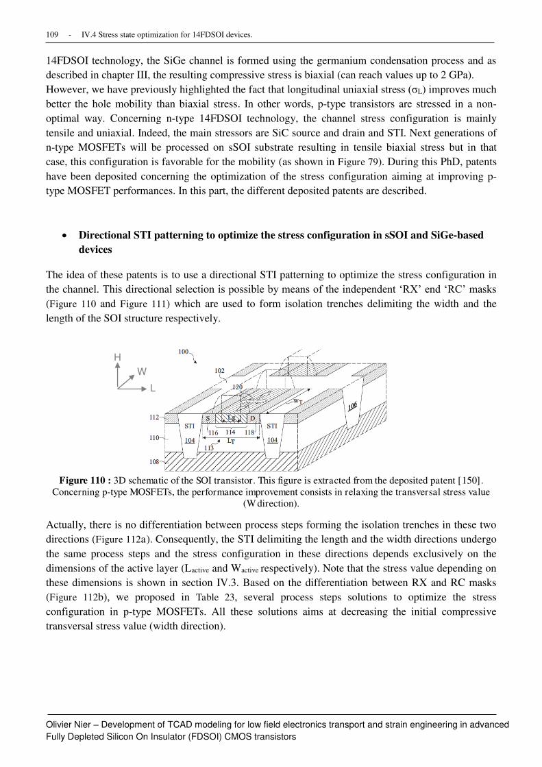
109 - IV.4 Stress state optimization for 14FDSOI devices.
Olivier Nier – Development of TCAD modeling for low field electronics transport and strain engineering in advanced
Fully Depleted Silicon On Insulator (FDSOI) CMOS transistors
14FDSOI technology, the SiGe channel is formed using the germanium condensation process and as
described in chapter III, the resulting compressive stress is biaxial (can reach values up to 2 GPa).
However, we have previously highlighted the fact that longitudinal uniaxial stress (σL) improves much
better the hole mobility than biaxial stress. In other words, p-type transistors are stressed in a non-
optimal way. Concerning n-type 14FDSOI technology, the channel stress configuration is mainly
tensile and uniaxial. Indeed, the main stressors are SiC source and drain and STI. Next generations of
n-type MOSFETs will be processed on sSOI substrate resulting in tensile biaxial stress but in that
case, this configuration is favorable for the mobility (as shown in Figure 79). During this PhD, patents
have been deposited concerning the optimization of the stress configuration aiming at improving p-
type MOSFET performances. In this part, the different deposited patents are described.
Directional STI patterning to optimize the stress configuration in sSOI and SiGe-based
devices
The idea of these patents is to use a directional STI patterning to optimize the stress configuration in
the channel. This directional selection is possible by means of the independent ‘RX’ end ‘RC’ masks
(Figure 110 and Figure 111) which are used to form isolation trenches delimiting the width and the
length of the SOI structure respectively.
Figure 110 : 3D schematic of the SOI transistor. This figure is extracted from the deposited patent [150].
Concerning p-type MOSFETs, the performance improvement consists in relaxing the transversal stress value
(W direction).
Actually, there is no differentiation between process steps forming the isolation trenches in these two
directions (Figure 112a). Consequently, the STI delimiting the length and the width directions undergo
the same process steps and the stress configuration in these directions depends exclusively on the
dimensions of the active layer (Lactive and Wactive respectively). Note that the stress value depending on
these dimensions is shown in section IV.3. Based on the differentiation between RX and RC masks
(Figure 112b), we proposed in Table 23, several process steps solutions to optimize the stress
configuration in p-type MOSFETs. All these solutions aims at decreasing the initial compressive
transversal stress value (width direction).
L
W
H

110 - CHAPTER IV. ST-oriented device applications
Olivier Nier – Development of TCAD modeling for low field electronics transport and strain engineering in advanced
Fully Depleted Silicon On Insulator (FDSOI) CMOS transistors
Figure 111 : a) Plan view of a RX mask used to form isolation trenches 106 delimiting the width of the SOI
structure. a) Plan view of a RC mask used to form isolation trenches 104 (STI) delimiting the length of the
structure. This figure is extracted from the deposited patent [150].
Figure 112 : Description of a) classical and b) proposed STI process steps.
Mask Process steps Comments
RX
SiGe channel (if SiGe first)
Hard mask deposition
STI etching
STI deposition Material mRX, deposition temperature TdRX
STI anneal Temperature TaRX, time tRX
Hard mask removal
SiGe channel (if SiGe last)
RC
SiGe channel (if SiGe first)
Hard mask deposition
STI etching
STI deposition Material mRC, deposition temperature TdRC
STI anneal Temperature TaRC, time tRC
Hard mask removal
SiGe channel (if SiGe last)
Table 23 : Description of the proposed STI process flow to optimize the stress configuration in MOSFETs

111 - IV.4 Stress state optimization for 14FDSOI devices.
Olivier Nier – Development of TCAD modeling for low field electronics transport and strain engineering in advanced
Fully Depleted Silicon On Insulator (FDSOI) CMOS transistors
The first idea concerns the SiGe channel formation. In part III.3.1, we demonstrated a strong reduction
of the stress relaxation when the channel is formed after STI process steps (SiGe last). Consequently, a
first solution can be proposed. It consists in forming the SiGe channel after STI formation steps
delimiting the length direction (Mask RC), as described in Figure 113. In this configuration, the
longitudinal stress undergo a lower relaxation because STI are formed before SiGe channel formation
(cf to part comparing SiGe first and last). Concerning the width direction, STI formation steps are
done after channel formation and consequently, a strong relaxation of the transversal stress occurs.
Figure 113 : Description of the proposed process flow to decrease the stress relaxation only in the length
direction only.
The second proposition concerns the STI deposition step where two alternative solutions can be used:
the deposited material and the temperature during the deposition can be different for trenches 106 and
104 (Figure 110). These two key parameters will influence the stress configuration through the thermal
deformation coefficient of the deposited STI materials. Thus, the stress in the longitudinal and
transversal directions can be adapted. The third idea deals with the STI anneal step. In that case, the
temperature and the durations of anneals can be adapted to promote the relaxation in one direction.
• Directional Implantation in STI for SiGe –based and sSOI-based devices.
The proposition is to use the directional STI patterning explained in the previous section to selectively
implant dopants in STI delimiting one direction and not in the second isolation trenches. The aim of
this implantation is to alter the viscosity of the STI as described in [149]. In our case, STI delimiting
the width are implanted to enhance the stress relaxation in this direction. An example of simplified
process flow is presented in Figure 114.

112 - CHAPTER IV. ST-oriented device applications
Olivier Nier – Development of TCAD modeling for low field electronics transport and strain engineering in advanced
Fully Depleted Silicon On Insulator (FDSOI) CMOS transistors
Figure 114 : Description of the proposed process flow to selectively implant trenches delimiting the width
direction to enhance the relaxation.
• Stress memory technique using directional STI masks for device performance
improvement.
Figure 115 : Cross section of the SOI transistor. This figure is extracted from the deposited patent [152]. The
step 414 corresponds to the implantation of Germanium atoms through trenches 412. Layer 112 is the
semiconductor, layer 110 the insulator and 404 and 406 correspond to hard mask layers.
This idea consists in using the directional STI patterning explained in the first deposited patent to
selectively amorphize the silicon region 416 (areas where STI will be formed). This amorphization can
be performed by implanting germanium at high energy level and dose (for example between 30 KeV
and 50 KeV, and at a density of between 1014 and 5x10¹⁴ atoms/cm3). It would lead to a tensile stress
being exerted by the regions 416 (Figure 15) into the portions of the semiconductor layer 112. The
phenomenon of stress induced by amorphization has been for example discussed in more detail in
[139]. While the stress is maintained in the semiconductor layer 112, an annealing operation is for
example performed to temporally decrease the viscosity of the hard mask nitride and the BOX
(corresponding to layer 110). By temporally decreasing the viscosity of the insulators, it relaxes such
that, when it cools again and the viscosity is increased, the stress in the semiconductor layer 112 is
maintained not only by the regions 416, but also by the underlying BOX layer and by the hard mask
stack (layers 406 and 404). Then, the depth of the trenches 412 is extended by a further etching step to
form the isolation trenches of Figure 106. In doing so, all or most of the germanium atoms implanted
into the semiconductor layer 112 are removed, and some relaxation of the semiconductor layer 112
occurs. However, due the presence of the BOX and the hard mask stack, a certain level of stress
should remain in the semiconductor layer 112.

113 - IV.5 Conclusion
Olivier Nier – Development of TCAD modeling for low field electronics transport and strain engineering in advanced
Fully Depleted Silicon On Insulator (FDSOI) CMOS transistors
In these part, we have explained the general content of the deposited patents. More details can be
found in [150] [151] [152].
IV.5 Conclusion
In the first part of this chapter, a brief description of the developed TCAD deck to model 14FDSOI
technology is performed. Then, in the second part, we present a full mechanical study of the stress
configuration in 14FDSOI technology through TCAD simulations and NBD measurements. Solutions
to optimize the stress configuration in sSOI and SiGe-based devices are proposed. We conclude that
while the integration of a piezoelectric layer in the BOX remains technologically difficult for a low
performance improvement, several solutions have been proposed to enhance devices performances.
These solutions are all based on the use of a directional STI patterning to differentiate the length and
the width directions. Thus, the stress in these two directions can be independently controlled by
adapting process steps according to propositions developed in section III.4.2. Independently, in this
chapter, we presented mechanical stress studies for 14FDSOI technology support such a as the impact
of SiGe source and drain on channel stress configuration.

114

115
Conclusions
Thesis summary:
Technological computer-aided design (TCAD) is a powerful tool to support technological
development within the industry. Indeed, TCAD support for FDSOI technology development can
reduce cost and development time but also secure technology choices. Based on STMicroelectronics
strategies, this PhD work aimed at developing the TCAD modeling for 28nm, 14nm and 10 nm
FDSOI devices, with a particular focus on stress engineering. From a process point of view, it has
consisted in developing a simulation methodology capable of reproducing accurately 14 nm FDSOI
process flow and the final topography of the device. An approach to model process-induced stress has
been set-up, focusing on the three main sources of stress in the device, namely SiGe channel, SiGe
source and drain, and material deposited at high temperature (such as STI and gate stack for example).
Concerning device simulation, a “top down” approach has been set-up. It has consisted in using
advanced physical-based solvers as a reference for TCAD empirical model calibration.
In more detail, in the first part of chapter 1, the main models implemented in state of the art device
simulators have been reviewed. First, a description of methodologies used to calculate the conduction
and valence band structure of silicon, germanium and silicon germanium alloy has been performed,
highlighting how stress and confinement are taken into account. In the second part, a multi-scale
strategy for MOSFET device modeling ranging from classical drift diffusion models to NEGF
calculation has been presented. In the last part, the models for the main scattering mechanisms in
semi-classical solvers such as MSMC or KG has been reviewed. The assumptions and range of
validity of these models have also been highlighted, and the developments of the in-house
STMicroelectronics KG solvers have been discussed.
Chapter 2 deals with a comparison of the different approaches currently available to model low field
transport in advanced Fully Depleted SOI transistors. Electron and hole mobilities have been
calculated using four different solvers: the STMicroelectonics in-house solver (UTOXPP), the
commercial solver Sband from Synopsys, the MSMC solver from the University of Udine and
TB_SIM, the NEGF solver from CEA. Simulations are then compared to split CV mobility
measurements performed on state of the art FDSOI devices. Using a large range of split-CV
measurements, the impact of the Equivalent Oxide Thicknesses (EOT), the back voltage and the
temperature have been investigated, leading to an extensive comparison between state of the art
models and experiments.
Chapter 3 aimed at describing the methodologies used during this thesis to model intentional and non-
intentional process induced stress. Simulations have been compared to nano-beam diffraction (NBD)
strain measurements at the nanometer scale. The second objective is to analyze and calibrate (on
advanced transport solvers) available TCAD models to efficiently account for the influence of stress
on mobility in a large level of stress (up to 2GPa). Finally, in this chapter, a complete methodology for
process-induced stress simulations and its impact on electrical characteristics has been set up. This
enables accurate and efficient TCAD simulations of strained-Si FDSOI MOSFETs in state of the art
CMOS technology. Chapter 4 presents applications of the previously presented methodologies to model advanced CMOS
devices. Mechanical simulations has been performed to model realistic stress profile in 14FDSOI

Olivier Nier – Development of TCAD modeling for low field electronics transport and strain engineering in advanced
Fully Depleted Silicon On Insulator (FDSOI) CMOS transistors 116
transistors from process simulation, with an emphasis on the modeling of the relaxation of the stress
during STI process steps and the effect of SiGe source and drain. Solutions to optimize the stress
configuration in sSOI and SiGe-based devices have been presented. These solutions are based on the
use of a directional STI patterning to differentiate the length and the width directions. Thus, the stress
in these two directions can be independently controlled by adapting process steps according to
propositions developed in chapter III.
Future works and recommendations:
This work has been focused so far on 28 nm and 14 nm FDSOI technologies featuring SiC/SiGe
source and drain and SiGe channel. However, additional technological solutions must be investigated
for 10nm FDSOI technology such as sSOI substrate, Germanium or III-V channel material. From a
process point of view, the stress configuration in the channel should be different and thus re-
optimized. From an electrical point of view, new mechanisms and challenges will appears. Examples
are listed below:
- Electrostatic and transport for III-V materials.
- Remote surface roughness scattering (with the high-k/IL interface).
- Remote phonon scattering.
- Source to drain tunneling.
Concerning the stress engineering, we highlighted in this manuscript that the strong stress relaxation
observed during STI patterning cannot be explained only by an elastic relaxation. It suggests that
another phenomenon further degrades the stress and is probably linked to the nature of the SiGe /
BOX interface. We suspect that the bonding between the SiGe layer and the BOX surface is weak and
cannot hold the stress in the channel during STI patterning. Further investigations concerning this
hypothesis should be performed. Other sources of stress (such as induced by silicidation for instance)
should also be considered.
Finally concerning the modeling of stress-induced mobility variation, a new model for surface
roughness should be developed and calibrated for the full range of effective field.

Olivier Nier – Development of TCAD modeling for low field electronics transport and strain engineering in advanced
Fully Depleted Silicon On Insulator (FDSOI) CMOS transistors 117
Annexes
Annexe I: Determination of the potential produced by a point charge
a) Analytical solution
The equation to solve is the following:
[ ∂∂z ϵ岫z岻 ∂∂z − ϵ岫z岻. Q態] G岫�, z, z待岻 = −e. げ岫z − z待岻 (I.1)
In previous UTOX version, an analytical solution was implemented.
Figure a1: Schematic of the studied 1D device.
A general solution of (I.1) for the potential can be expressed in the three materials of Figure a1 in the
form:
G岫�, z, z待岻 = − なに� ∗ { a単e−濯|炭−炭轍| + b単e−濯|炭+炭轍| 岫z < ど岻c単e濯岫炭+炭轍岻 + d単e−濯岫炭−炭轍岻 岫ど 判 z 判 �岻f単e−濯岫炭−炭轍岻 岫z 半 �岻 (I.2)
And the boundary conditions are:
{G濯岫z = ど−, z待岻 = G濯岫z = ど+, z待岻 G濯岫z = �−, z待岻 = G濯岫z = �+, z待岻 (I.3)
{ κdG濯岫z = ど−, z待岻dz = ϵ辿 dG濯岫z = ど+, z待岻dzϵ辿 dG濯岫z = �−, z待岻dz = ϵ坦 dG濯岫z = �+, z待岻dz (I.4)
dG濯岫z = z待+, z待岻dz − dG濯岫z = z待−, z待岻dz = −な (I.5)
Eq. I.5 implies a単 = な and Eq. I.3 and Eq.I.4 gives:
{ な + b濯 = c濯 + d濯c単e濯担 + d濯e−濯担 = f濯e−濯担な − b濯 = ϵ辿κ 岫d濯 − c濯岻c濯e濯担 − d濯e−濯担 = − ϵ坦ϵ辿 f濯e−濯担
(I.6)
0 t z
HfO2 SiO2 Si

Olivier Nier – Development of TCAD modeling for low field electronics transport and strain engineering in advanced
Fully Depleted Silicon On Insulator (FDSOI) CMOS transistors 118
蛮な −κ/ϵ辿 −κ/ϵ辿 どな −な な どど e濯担 e−濯担 −ϵ辿/ϵ坦e−濯担ど e濯担 −e−濯担 e−濯担 ) ∗ ( b単c単d単f単)
= 蛮−ななどど ) (I.7)
In [86], this system is solved numerically to find coefficients b単, c単, d単 and f単.
The calculation of the Green function using this method implies two major drawbacks. The first is that
only three materials (with different ε) can be treated and consequently, our Green function is inaccurate in the case of high-k FDSOI devices (we actually treat only the three materials: high-k, IL and Si). The
second drawback concerns the boundary conditions: layers at each sides of the simulation domain are
considered as infinitely thick. It is however important in the case of high-k metal gate devices to set G
to zero since the metal gate screens the potential.
In order to treat the general case, i.e. an infinite number of layers with different ε, we can use the finite difference method to solve the equation. In part II, this method is applied to a non-uniform grid.
b) Finite difference method
[ ∂∂z ϵ岫z岻 ∂∂z − ϵ岫z岻. Q態] G岫�, z, z待岻 = げ岫z − z待岻
(II.1)
G′′岫z岻 ∗ ϵ岫z岻 + ϵ′岫z岻. G′岫z岻 − ϵ岫z岻. Q態. G岫z岻 = げ岫z − z待岻 (II.2)
For non-uniform grid, G′′and G′ can be expressed from Taylor expansion:
G岫z辿 + な岻 = G岫z辿岻 + G′岫z辿岻. �辿+ + G′′岫z辿岻に . 岫�辿+岻² (II.3)
G岫z辿 − な岻 = G岫z辿岻 − G′岫z辿岻. �辿− + G′′岫z辿岻に . 岫�辿−岻² (II.4)
After multiplying �辿− to (II.3) and �辿+ to (II.4), and summing:
G′′岫z辿岻 = に. �辿−. G岫z辿 + な岻 + �辿+. G岫z辿 − な岻 − 岫�辿+ + �辿−岻G岫z辿岻岫�辿−岻². �辿+ + 岫�辿+岻². �辿− (II.5)
G′′岫z辿岻 = に. �辿−�辿+ . G岫z辿 + な岻 + G岫z辿 − な岻 − (な + �辿−�辿+) G岫z辿岻岫�辿−岻. 岫 �辿+ + �辿−岻 (II.6)
And:
G′岫z辿岻 = G岫z辿 + な岻 − G岫z辿 − な岻 �辿+ + �辿− (II.7)
G′岫z辿岻 = �辿−. G岫z辿 + な岻 − �辿−. G岫z辿 − な岻 岫�辿−岻. 岫 �辿+ + �辿−岻 (II.8)

Olivier Nier – Development of TCAD modeling for low field electronics transport and strain engineering in advanced
Fully Depleted Silicon On Insulator (FDSOI) CMOS transistors 119
Applying the approximations (II.6) and (II.8) to Eq.II.2, we can determine the finite difference
equation:
に. �辿−�辿+ . G岫z辿 + な岻 + G岫z辿 − な岻 − (な + �辿−�辿+) G岫z辿岻岫�辿−岻. 岫 �辿+ + �辿−岻 + ϵ′岫z辿岻ϵ岫z辿岻 . �辿−. G岫z辿 + な岻 − �辿−. G岫z辿 − な岻 岫�辿−岻. 岫 �辿+ + �辿−岻 − Q態G岫z辿岻 = げ岫z − z待岻ϵ岫z辿岻
Multiplying by 岫�辿−岻. 竪套++竪套−態 gives:
�辿−�辿+ . G岫z辿 + な岻 + G岫z辿 − な岻 − 峭な + �辿−�辿+嶌G岫z辿岻 + ϵ′岫z辿岻に. ϵ岫z辿岻 . 岫�辿−. G岫z辿 + な岻 − �辿−. G岫z辿 − な岻岻 − Q態. 岫�辿−岻. 岫 �辿+ + �辿−岻に . G岫z辿岻= げ岫z − z待岻に. ϵ岫z辿岻 . 岫�辿−岻. 岫 �辿+ + �辿−岻 So:
峭な − ϵ′岫z辿岻. �辿−岻に. ϵ岫z辿岻 嶌 . G岫z辿 − な岻 − [峭な + �辿−�辿+嶌 + Q態. 岫�辿−岻. 岫 �辿+ + �辿−岻に ] . G岫z辿岻 + [�辿−�辿+ + ϵ′岫z辿岻. �辿−岻に. ϵ岫z辿岻 ] G岫z辿 + な岻= げ岫z − z待岻に. ϵ岫z辿岻 . 岫�辿−岻. 岫 �辿+ + �辿−岻
(II.9)
This equation has the form: b辿. G岫z辿 − な岻 + d辿. G岫z辿岻 + a辿. G岫z辿 − な岻 = げ岫z − z待岻. f辿
With { b辿 = な − ϵ′岫炭套岻.竪套−態.ϵ岫炭套岻d辿 = −(な + 竪套−竪套+) − 濯鉄.岫竪套−岻.岫 竪套++竪套−岻態a辿 = 竪套−竪套+ + ϵ′岫炭套岻.竪套−岻態.ϵ岫炭套岻
and f辿 = 岫�辿−岻. ( 竪套++竪套−匪態.ϵ岫炭套岻
So eq.II.1 takes the form:
AG = げ. f (II.10)
���� A =( d待 a待 ど 橋 橋 どb怠 d怠 a怠 ⋱ 教ど b態 d態 a態 ⋱ 教教 ⋱ ⋱ ⋱ ⋱ ど教 ⋱ ⋱ d択−態 a択−態ど 橋 橋 ど b択−態 d択−怠)
(II.11)
and げ = 岫ど 橋 ど げ辿丹 ど 橋 ど岻鐸 げ辿丹 = 岫�辿丹− 岻. ( �辿丹+ + �辿丹− 匪に. ϵ(z辿丹匪
Boundary conditions:

Olivier Nier – Development of TCAD modeling for low field electronics transport and strain engineering in advanced
Fully Depleted Silicon On Insulator (FDSOI) CMOS transistors 120
The Dirichlet boundary conditions are imposed by setting the two values of the potential at each
extremity. G岫ど岻 = �待 and G岫N − な岻 = �択−怠
In our case, the potential is fixed to zero at each sides.
Matlab implementation:
Using Matlab, we can solve Eq.II.10 numerically 岫G = �nθ岫A岻 ∗ げ岻. It is however CPU time
consuming.
An analytical solution to inverse trigonal matrices has been developed in [El-Mikkawy-06] and applied
to this equation in [87]. Three vectors are defined as:
ゎ辿 = { な �f � = ど d待 �f � = なd辿−怠ゎ辿−怠 − b辿−怠a辿−態ゎ辿−態 �f � = に,ぬ,ね, … . N
が辿 = { な �f � = N d択−怠 �f � = なd辿が辿+怠 − b辿+怠a辿が辿+態 �f � = N − に, N − ぬ,…
η辿 = { が怠d待が怠 − b怠a待が態 �f � = どゎ択−怠d択−怠ゎ択−怠 − b択−怠a択−態ゎ択−態 �f � = N − なが辿+怠ゎ辿d辿が辿+怠ゎ辿 − b辿a辿−怠が辿+怠ゎ辿−怠 − b辿+怠a辿が辿+態ゎ辿 o��e����e
The Green’s function is finally obtained by:
G辿 ={ げ辿丹ゎ辿η辿丹岫−な岻辿丹−辿∏ a辿丹−谷辿丹−辿谷=待ゎ辿丹 �f � < 件喧η辿丹げ辿丹 �f � = �� �f � = ��げ辿丹が辿+怠η辿丹岫−な岻辿−辿丹∏ b辿丹+谷辿−辿丹谷=待が辿丹+怠 �f � > 件喧
(II.12)

Olivier Nier – Development of TCAD modeling for low field electronics transport and strain engineering in advanced
Fully Depleted Silicon On Insulator (FDSOI) CMOS transistors 121
Annexe 2: Sdevice syntax for TCAD drift diffusion device simulations
The syntax describing the physic models in the channel region is shown in figure a2. This includes:
- Generation recombination models (Shockley-Read-Hall and Auger mechanisms)
- A band gap model (EffectiveIntrinsecDensity)
- Density-gradient quantization model (eQuantumPotential hQuantumPotential)
- Mobility models accounting for bulk mobility (PhuMob corresponds to Philips unified mobility
model [100]) for degradation of the mobility in thin films (ThinLayer), for mobility degradation
due to charge at high-k/IL interface
Figure a2: Description of the Sdevice models describing the physics in the channel region.

Olivier Nier – Development of TCAD modeling for low field electronics transport and strain engineering in advanced
Fully Depleted Silicon On Insulator (FDSOI) CMOS transistors 122

123

Olivier Nier – Development of TCAD modeling for low field electronics transport and strain engineering in advanced
Fully Depleted Silicon On Insulator (FDSOI) CMOS transistors 124
Bibliography:
[1] http://www.itrs.net
[2] G. E. Moore. Cramming more components onto integrated circuits. Electronics Magazine, 38 (8):
114-117.
[3] Faynot, O., Andrieu, F., Weber, O., Fenouillet-Béranger, C., Perreau, P., Mazurier, J., ... &
Deleonibus, S. (2010, December). Planar Fully depleted SOI technology: A Powerful architecture
for the 20nm node and beyond. In Electron Devices Meeting (IEDM), 2010 IEEE International
(pp. 3-2). IEEE.
[4] Mizuno, T., Takagi, S., Sugiyama, N., Satake, H., Kurobe, A., & Toriumi, A. (2000). Electron and
hole mobility enhancement in strained-Si MOSFET's on SiGe-on-insulator substrates fabricated by
SIMOX technology. Electron Device Letters, IEEE, 21(5), 230-232.
[5] Heyns, M., & Tsai, W. (2009). Ultimate scaling of CMOS logic devices with Ge and III–V
materials. Mrs bulletin, 34(07), 485-492.
[6] Rideau, D., Feraille, M., Ciampolini, L., Minondo, M., Tavernier, C., Jaouen, H., & Ghetti, A.
(2006). Strained Si, Ge, and Si 1− x Ge x alloys modeled with a first-principles-optimized full-
zone k∙ p method. Physical Review B, 74(19), 195208. [7] Jancu, J. M., Scholz, R., Beltram, F., & Bassani, F. (1998). Empirical spds* tight-binding
calculation for cubic semiconductors: General method and material parameters. Physical Review
B, 57(11), 6493.
[8] Luisier, M., Schenk, A., Fichtner, W., & Klimeck, G. (2006). Atomistic simulation of nanowires in
the s p 3 d 5 s* tight-binding formalism: From boundary conditions to strain calculations. Physical
Review B, 74(20), 205323.
[9] Cohen, M. L., & Bergstresser, T. K. (1966). Band structures and pseudopotential form factors for
fourteen semiconductors of the diamond and zinc-blende structures. Physical Review, 141(2), 789.
[10] Luttinger, J. M., and W. Kohn. "Motion of electrons and holes in perturbed periodic fields."
Physical Review 97.4 (1955): 869.
[11] Van de Walle, Chris G. "Band lineups and deformation potentials in the model-solid theory."
Physical Review B 39.3 (1989): 1871.
[12] Fischetti, Max V., and Steven E. Laux. "Band structure, deformation potentials, and carrier
mobility in strained Si, Ge, and SiGe alloys." Journal of Applied Physics 80.4 (1996): 2234-2252.
[13] Rieger, M. M., & Vogl, P. (1993). Electronic-band parameters in strained Si 1-x Ge x alloys on
Si 1-y Ge y substrates. Physical Review B, 48(19), 14276.
[14] Zlatan Stanojevic. PhD thesis.
[15] G. Dresselhaus, A. F. Kip, and C. Kittel. Cyclotron Resonance of Electrons and Holes in
Silicon and Germanium Crystals. Phys. Rev., 98:368{384, Apr 1955.G.
[16] Luttinger, J. M. (1956). Quantum theory of cyclotron resonance in semiconductors: General
theory. Physical Review, 102(4), 1030.
[17] E. Pikus and G. L. Bir. "Effect of deformation on the hole energy spectrum of Germanium and
Silicon". Sov. Phys.-Solid state, 1:1502, 1959.
[18] Chelikowsky, J. R., & Cohen, M. L. (1974). Electronic structure of silicon. Physical Review B,
10(12), 5095.
[19] Ferry, D. (2001). Quantum mechanics: an introduction for device physicists and electrical
engineers. CRC Press.
[20] Bardeen, J., and W. Shockley. "Deformation potentials and mobilities in non-polar crystals."
Physical Review 80.1 (1950): 72.
[21] Grasser, T., Tang, T. W., Kosina, H., & Selberherr, S. (2003). A review of hydrodynamic and
energy-transport models for semiconductor device simulation. Proceedings of the IEEE, 91(2),
251-274.

Olivier Nier – Development of TCAD modeling for low field electronics transport and strain engineering in advanced
Fully Depleted Silicon On Insulator (FDSOI) CMOS transistors 125
[22] Selberherr, S. (2012). Analysis and simulation of semiconductor devices. Springer Science &
Business Media.
[23] Canali, C., Majni, G., Minder, R., & Ottaviani, G. (1975). Electron and hole drift velocity
measurements in silicon and their empirical relation to electric field and temperature. Electron
Devices, IEEE Transactions on, 22(11), 1045-1047.
[24] Stratton, R. (1962). Diffusion of hot and cold electrons in semiconductor barriers. Physical
Review, 126(6), 2002.
[25] Blotekjaer, K. (1970). Transport equations for electrons in two-valley semiconductors.
Electron Devices, IEEE Transactions on, 17(1), 38-47.
[26] Gritsch, M., Kosina, H., Grasser, T., & Selberherr, S. (2002). Revision of the standard
hydrodynamic transport model for SOI simulation. IEEE Transactions on Electron Devices,
49(10), 1814-1820.
[27] Grasser, T., Jungemann, C., Kosina, H., Meinerzhagen, B., & Selberherr, S. (2004). Advanced
transport models for sub-micrometer devices (pp. 1-8). Springer Vienna.
[28] Jacoboni, C., & Reggiani, L. (1983). The Monte Carlo method for the solution of charge
transport in semiconductors with applications to covalent materials. Reviews of Modern Physics,
55(3), 645.
[29] Fischetti, M. V., & Laux, S. E. (1988). Monte Carlo analysis of electron transport in small
semiconductor devices including band-structure and space-charge effects. Physical Review B,
38(14), 9721.
[30] Venturi, F., Smith, R. K., Sangiorgi, E. C., Pinto, M. R., & Ricco, B. (1989). A general purpose
device simulator coupling Poisson and Monte Carlo transport with applications to deep submicron
MOSFETs. Computer-Aided Design of Integrated Circuits and Systems, IEEE Transactions on,
8(4), 360-369.
[31] Lucci, L. Modeling of advanced nanometer scale MOSFETs devices with the multi-subband
Monte Carlo approach. PhD thesis. Université de Grenoble. 2007.
[32] Datta, S. (2000). Nanoscale device modeling: the Green’s function method. Superlattices and microstructures, 28(4), 253-278.
[33] Herring, Conyers, and Erich Vogt. "Transport and deformation-potential theory for many-
valley semiconductors with anisotropic scattering." Physical Review 101.3 (1956): 944.
[34] Jin, S., Fischetti, M. V, & Tang, T. (2007). Modeling of Surface-Roughness Scattering in
Ultrathin-Body SOI MOSFETs. IEEE Transactions on Electron Devices, 54(9), 2191–2203.
[35] Ungersboeck, E., Dhar, S., Karlowatz, G., Sverdlov, V., Kosina, H., & Selberherr, S. (2007).
The effect of general strain on the band structure and electron mobility of silicon. Electron
Devices, IEEE Transactions on, 54(9), 2183-2190.
[36] Sentaurus Device Monte Carlo User Guide . Version H-2013.03, March 2013. SYNOPSYS.
[37] Toniutti, P., Esseni, D., & Palestri, P. (2010). Failure of the scalar dielectric function approach
for the screening modeling in double-gate SOI MOSFETs and in FinFETs. Electron Devices, IEEE
Transactions on, 57(11), 3074-3083.
[38] Niquet, Y., Nguyen, V., Triozon, F., Duchemin, I., Rideau, D., & Nier, O. (2014). Quantum
calculations of the carrier mobility in thin films: Methodology, Matthiessen’s rule and comparison
with semi-classical approaches. Journal of Applied Physics, 115(5), 054512.
[39] Rideau, D., Niquet, Y. M., Nier, O., Palestri, P., Esseni, D., Nguyen, V. H., ... & Smith, L.
(2012). Mobility in FDSOI devices: Monte Carlo and Kubo Greenwood approaches compared to
NEGF simulations.
[40] Rideau, D., et al. "Mobility in high-K metal gate UTBB-FDSOI devices: From NEGF to
TCAD perspectives " Electron Devices Meeting (IEDM), 2013 IEEE International. IEEE, 2013.

Olivier Nier – Development of TCAD modeling for low field electronics transport and strain engineering in advanced
Fully Depleted Silicon On Insulator (FDSOI) CMOS transistors 126
[41] Esseni, D., Abramo, A., Selmi, L., & Sangiorgi, E. (2002). Study of low field electrons
transport in ultra-thin single and double gate SOI MOSFETs. Electron Devices Meeting (IEDM),
719–722.
[42] Esseni, D., & Sangiorgi, E. (2004). Low field electron mobility in ultra-thin SOI MOSFETs:
experimental characterization and theoretical investigation. Solid-State Electronics, 48(6), 927–936. doi:10.1016/j.sse.2003.12.027
[43] Osgnach, P., Revelant, A., Lizzit, D., Palestri, P., Esseni, D., & Selmi, L. (2013). Toward
computationally efficient Multi-Subband Monte Carlo Simulations of Nanoscale MOSFETs. Proc.
SISPAD, 176–179.
[44] Takagi, S., Toriumi, A., Iwase, M., & Tango, H. (1994). On the Universality of Inversion
Layer Mobility in Si MOSFET ’ s : Part I-Effects of Substrate Impurity Concentration. IEEE
Electron Device Letters, 41(12), 2357–2362.
[45] Prange, R. E., & Nee, T. W. (1968). Quantum spectroscopy of the low-field oscillations in the
surface impedance. Physical Review, 168(3), 779.
[46] Esseni, D. (2004). On the Modeling of Surface Roughness Limited Mobility in SOI MOSFETs
and Its Correlation to the Transistor Effective Field. IEEE Transactions on Electron Devices,
51(3), 394–401.
[47] Esseni, D., Palestri, P., & Selmi, L. (2011). Nanoscale MOS Transistors. Cambridge University
Press, Cambridge.
[48] Bonno, O., Barraud, S., Mariolle, D., & Andrieu, F. (2008). Effect of strain on the electron
effective mobility in biaxially strained silicon inversion layers: An experimental and theoretical
analysis via atomic force microscopy measurements and Kubo-Greenwood mobility calculations.
Journal of Applied Physics, 103(6), 063715.
[49] Pirovano, A., Lacaita, A. L., Ghidini, G., & Tallarida, G. (2000). On the correlation between
surface roughness and inversion layer mobility in Si-MOSFETs. Electron Device Letters, IEEE,
21(1), 34-36.
[50] Yamanaka, T., Fang, S. J., Lin, H. C., Snyder, J. P., & Helms, C. R. (1996). Correlation
between inversion layer mobility and surface roughness measured by AFM. Electron Device
Letters, IEEE, 17(4), 178-180.
[51] Fischetti, M. V., & Laux, S. E. (1993). Monte Carlo study of electron transport in silicon
inversion layers. Physical Review B, 48(4), 2244.
[52] Nier, O., Rideau, D., Niquet, Y. M., Monsieur, F., Nguyen, V. H., Triozon, F., Cros, A., Clerc,
R., Barbé, JC., Palestri, P., Esseni, D., Duchemin, I., Smith,L. , Silvestri, L., Nallet, F., Tavernier,
C., Jaouen, H., Selmi, L. (2013). Multi-scale strategy for high-k/metal-gate UTBB-FDSOI devices
modeling with emphasis on back bias impact on mobility. Journal of Computational Electronics,
12(4), 675-684.
[53] Yamakawa, S., Ueno, H., Taniguchi, K., Hamaguchi, C., Miyatsuji, K., Masaki, K., &
Ravaioli, U. (1996). Study of interface roughness dependence of electron mobility in Si inversion
layers using the Monte Carlo method. Journal of applied physics, 79(2), 911-916.
[54] Lizzit, D., Esseni, D., Palestri, P., & Selmi, L. (2013, December). Surface roughness limited
mobility modeling in ultra-thin SOI and quantum well III-V MOSFETs. In Electron Devices
Meeting (IEDM), 2013 IEEE International (pp. 5-2). IEEE.
[55] Baum, R. F. (1969). The correlation function of Gaussian noise passed through nonlinear
devices. Information Theory, IEEE Transactions on, 15(4), 448-456.
[56] Shah, R., & De Souza, M. M. (2009). Scattering at MOS Interfaces. In Proceedings of the
World Congress on Engineering (Vol. 1).
[57] Cristoloveanu, S., Rodriguez, N., & Gamiz, F. (2010). Why the universal mobility is not.
Electron Devices, IEEE Transactions on 57.6: 1327-1333.

Olivier Nier – Development of TCAD modeling for low field electronics transport and strain engineering in advanced
Fully Depleted Silicon On Insulator (FDSOI) CMOS transistors 127
[58] Ohata, A., et al. Impact of back-gate biasing on effective field and mobility in ultrathin silicon-
on-insulator metal-oxide-semiconductor field-effect-transistors. Journal of Applied Physics 113.14
(2013): 144514-144514
[59] Sherony, M. J., Su, L. T., Chung, J. E., & Antoniadis, D. A. (1994). SOI MOSFET effective
channel mobility. Electron Devices, IEEE Transactions on, 41(2), 276-278.
[60] Sabnis, A. G., & Clemens, J. T. (1979). Characterization of the electron mobility in the
inverted< 100> Si surface. In Electron Devices Meeting, 1979 Internationa (Vol. 25, pp. 18-21).
IEEE.
[61] Esseni, D., Mastrapasqua, M., Celler, G. K., Fiegna, C., Selmi, L., & Sangiorgi, E. (2003). An
experimental study of mobility enhancement in ultrathin SOI transistors operated in double-gate
mode. Electron Devices, IEEE Transactions on, 50(3), 802-808.
[62] Palestri, P., Alexander, C., Asenov, A., Aubry-Fortuna, V., Baccarani, G., Bournel, A., ... &
Walczak, J. (2009). A comparison of advanced transport models for the computation of the drain
current in nanoscale nMOSFETs. Solid-State Electronics, 53(12), 1293-1302.
[63] Abramo, A., Baudry, L., Brunetti, R., Castagne, R., Charef, M., Dessenne, F., ... & Yoshii, A.
(1994). A comparison of numerical solutions of the Boltzmann transport equation for high-energy
electron transport silicon. Electron Devices, IEEE Transactions on, 41(9), 1646-1654.
[64] Esseni, D., & Driussi, F. (2011). A Quantitative Error Analysis of the Mobility Extraction
According to the Matthiessen Rule in Advanced MOS Transistors. IEEE Electron Device Letters,
58(8), 2415–2422.
[65] Garetto, D., Rideau, D., Tavernier, C., Leblebiciand, Y., Schmid, A., & Jaouen, H. (2011).
Advanced physics for simulation of ultrascaled devices with UTOXPP solver. In Proceedings of
the 14th International Nanotech Conference (Vol. 3, No. EPFL-CONF-169896).
[66] http://www.synopsys.com/Tools/TCAD/
[67] Esseni, D., Palestri, P., & Selmi, L. (2011). Nanoscale MOS Transistors. Cambridge University
Press, Cambridge
[68] http://inac.cea.fr/L_Sim/TB_Sim/
[69] Fenouillet-Beranger, C., Denorme, S., Icard, B., Boeuf, F., Coignus, J., Faynot, O., ... &
Deleombus, S. (2007, December). Fully-depleted SOI technology using high-k and single-metal
gate for 32 nm node LSTP applications featuring 0.179 μm 2 6T-SRAM bitcell. In Electron
Devices Meeting, 2007. IEDM 2007. IEEE International (pp. 267-270). IEEE.
[70] Fenouillet-Beranger, C., Denorme, S., Perreau, P., Buj, C., Faynot, O., Andrieu, F., ... &
Skotnicki, T. (2009). FDSOI devices with thin BOX and ground plane integration for 32nm node
and below. Solid-State Electronics, 53(7), 730-734.
[71] Andrieu F, Dupré C, Rochette F, Faynot O, Tosti L, Buj C, et al, “25 nm short and narrow strained FDSOI with TiN/HfO2 gate stack”. IEEE VLSI symp tech dig.
[72] Cassé M, Thevenod L, Guillaumot B, Tosti L, Martin F, Mitard
[73] J, et al, “Carrier transport in HfO2/metal gate MOSFETs: physical insight into critical
parameters”. IEEE Trans Electron
[74] Dev 2006;53(4):759–68.
[75] Planes, N., Weber, O., Barral, V., Haendler, S., Noblet, D., Croain, D., ... & Haond, M. (2012,
June). 28nm FDSOI technology platform for high-speed low-voltage digital applications. In VLSI
Technology (VLSIT), 2012 Symposium on (pp. 133-134). IEEE.
[76] Cassé, M., Thevenod, L., Guillaumot, B., Tosti, L., Martin, F., Mitard, J., ... & Boulanger, F.
(2006). Carrier transport in HfO2/metal gate MOSFETs: physical insight into critical parameters.
Electron Devices, IEEE Transactions on, 53(4), 759-768

Olivier Nier – Development of TCAD modeling for low field electronics transport and strain engineering in advanced
Fully Depleted Silicon On Insulator (FDSOI) CMOS transistors 128
[77] Gamiz, F., & Fischetti, M. V. (2003). Remote Coulomb scattering in metal–oxide–semiconductor field effect transistors: Screening by electrons in the gate. Applied physics letters,
83(23), 4848-4850.
[78] Fischetti, M. V. (2001). Long-range Coulomb interactions in small Si devices. Part II. Effective
electron mobility in thin-oxide structures. Journal of Applied Physics, 89(2), 1232-1250.
[79] Esseni, D., & Abramo, A. (2003). Modeling of electron mobility degradation by remote
Coulomb scattering in ultrathin oxide MOSFETs. Electron Devices, IEEE Transactions on, 50(7),
1665-1674.
[80] Hinckley, J. M., & Singh, J. (1990). Hole transport theory in pseudomorphic Si 1− x Ge x alloys grown on Si (001) substrates. Physical Review B, 41(5), 2912.
[81] Pham, A. T., Jungemann, C., & Meinerzhagen, B. (2007). Physics-based modeling of hole
inversion-layer mobility in strained-SiGe-on-insulator. Electron Devices, IEEE Transactions on,
54(9), 2174-2182.
[82] Mehrotra, S. R., Paul, A., & Klimeck, G. (2011). Atomistic approach to alloy scattering in Si1− xGex. Applied Physics Letters, 98(17), 173503.
[83] Briggs, P. J., Walker, A. B., & Herbert, D. C. (1998). Calculation of hole mobilities in relaxed
and strained SiGe by Monte Carlo simulation. Semiconductor science and technology, 13(7), 680.
[84] Lizzit, D., Palestri, P., Esseni, D., Revelant, A., & Selmi, L. (2013). Analysis of the
performance of n-type FinFETs with strained SiGe channel. Electron Devices, IEEE Transactions
on, 60(6), 1884-1891.
[85] Esseni, D., Abramo, A., Selmi, L., & Sangiorgi, E. (2003). Physically based modeling of low
field electron mobility in ultrathin single-and double-gate SOI n-MOSFETs. Electron Devices,
IEEE Transactions on, 50(12), 2445-2455.
[86] Barraud, S., Bonno, O., & Cassé, M. (2008). The influence of Coulomb centers located in HfO[sub 2]/SiO[sub 2] gate stacks on the effective electron mobility. Journal of Applied Physics,
104(7), 073725. doi:10.1063/1.2968217
[87] Casterman, D., & De Souza, M. M. (2010). Evaluation of the Coulomb-limited mobility in
high-κ dielectric metal oxide semiconductor field effect transistors. Journal of Applied Physics,
107(6), 063706. doi:10.1063/1.3319558
[88] Toniutti, P., Palestri, P., Esseni, D., Driussi, F., De Michielis, M., & Selmi, L. (2012). On the
origin of the mobility reduction in n- and p-metal–oxide–semiconductor field effect transistors
with hafnium-based/metal gate stacks. Journal of Applied Physics, 112(3), 034502.
[89] Fischetti, Massimo V., Deborah A. Neumayer, and Eduard A. Cartier. "Effective electron
mobility in Si inversion layers in metal–oxide–semiconductor systems with a high-κ insulator: The
role of remote phonon scattering." Journal of Applied Physics 90.9 (2001): 4587-4608.
[90] Gmiz, F., & Roldn, J. B. (2003). Scattering of electrons in silicon inversion layers by remote surface roughness. Journal of Applied Physics, 94(1), 392. doi:10.1063/1.1577227
[91] Zhang, X. F., Xu, J. P., Lai, P. T., & Li, C. X. (2007). A Physical Model on Scattering at High-
κ Dielectric/SiO 2 Interface of SiGe p-MOSFETs. Electron Devices, IEEE Transactions on,
54(11), 3097-3102.
[92] Ghosh, B., Chen, J. H., Fan, X. F., Register, L. F., & Banerjee, S. K. (2006). Monte Carlo
study of remote Coulomb and remote surface roughness scattering in nanoscale Ge PMOSFETs
with ultrathin high-κ dielectrics. Solid-state electronics, 50(2), 248-253.
[93] Lundstrom, M. (2009). Fundamentals of carrier transport. Cambridge University Press.
[94] da Stefano Poli, P. (2009). MODELLING AND SIMULATIONS OF POST–CMOS
DEVICES.

Olivier Nier – Development of TCAD modeling for low field electronics transport and strain engineering in advanced
Fully Depleted Silicon On Insulator (FDSOI) CMOS transistors 129
[95] Ernst, T., Cristoloveanu, S., Ghibaudo, G., Ouisse, T., Horiguchi, S., Ono, Y., ... & Murase, K.
(2003). Ultimately thin double-gate SOI MOSFETs. Electron Devices, IEEE Transactions on,
50(3), 830-838.
[96] Klaassen, D. B. M. (1990, December). A unified mobility model for device simulation. In
Electron Devices Meeting, 1990. IEDM'90. Technical Digest., International (pp. 357-360). IEEE.
[97] Bennamane, K., Ghibaudo, G., & Benfdila, A. (2009). Method for extraction of η parameter characterising μ eff against E eff curves in FD-SOI Si MOS devices. Electronics letters, 45(12),
655-657.
[98] Van Den Daele, W., Le Royer, C., Augendre, E., Mitard, J., Ghibaudo, G., & Cristoloveanu, S.
(2011). Detailed investigation of effective field, hole mobility and scattering mechanisms in GeOI
and Ge pMOSFETs. Solid-State Electronics, 59(1), 25-33.
[99] Reggiani, S., Gnani, E., Gnudi, A., Rudan, M., & Baccarani, G. (2007). Low-field electron
mobility model for ultrathin-body SOI and double-gate MOSFETs with extremely small silicon
thicknesses. Electron Devices, IEEE Transactions on, 54(9), 2204-2212.
[100] Sentaurus Device User Guide. Version H-2013.03. SYNOPSYS
[101] Ito, S., Namba, H., Yamaguchi, K., Hirata, T., Ando, K., Koyama, S., ... & Horiuchi, T. (2000,
December). Mechanical stress effect of etch-stop nitride and its impact on deep submicron
transistor design. In Electron Devices Meeting, 2000. IEDM'00. Technical Digest. International
(pp. 247-250). IEEE.
[102] Shimizu, A., Hachimine, K., Ohki, N., Ohta, H., Koguchi, M., Nonaka, Y., ... & Ootsuka, F.
(2001, December). Local mechanical-stress control (LMC): A new technique for CMOS-
performance enhancement. In Electron Devices Meeting, 2001. IEDM'01. Technical Digest.
International (pp. 19-4). IEEE.
[103] Gannavaram, S., Pesovic, N., & Ozturk, C. (2000, December). Low temperature (800/spl
deg/C) recessed junction selective silicon-germanium source/drain technology for sub-70 nm
CMOS. In Electron Devices Meeting, 2000. IEDM'00. Technical Digest. International (pp. 437-
440). IEEE.
[104] Liu, Q., Vinet, M., Gimbert, J., Loubet, N., Wacquez, R., Grenouillet, L., ... & Sampson, R.
(2013, December). High performance UTBB FDSOI devices featuring 20nm gate length for 14nm
node and beyond. In Electron Devices Meeting (IEDM), 2013 IEEE International (pp. 9-2). IEEE.
[105] Andrieu, F., Casse, M., Baylac, E., Perreau, P., Nier, O., Rideau, D., Berthelon, R., Pourchon,
F., Pofelski, A., De Salvo, B., Gallon, C., Mazzocchi,, V., Barge, D., Gaumer, C., Gourhant, O.,
Cros, A., Barral, V., Ranica, R., Planes, N., Schwarzenbach, W., Richard, E., Josse, E., Weber, O.,
Arnaud, F., Vinet, M., Faynot, O., Haond, M. (2014, September). Strain and layout management in
dual channel (sSOI substrate, SiGe channel) planar FDSOI MOSFETs. In Solid State Device
Research Conference (ESSDERC), 2014 44th European (pp. 106-109). IEEE.
[106] Weber, O., Irisawa, T., Numata, T., Harada, M., Taoka, N., Yamashita, Y., ... & Takagi, S.
(2007, December). Examination of additive mobility enhancements for uniaxial stress combined
with biaxially strained Si, biaxially strained SiGe and Ge channel MOSFETs. In Electron Devices
Meeting, 2007. IEDM 2007. IEEE International (pp. 719-722). IEEE.
[107] People, R., & Bean, J. C. (1985). Calculation of critical layer thickness versus lattice mismatch
for GexSi1− x/Si strained‐layer heterostructures. Applied Physics Letters, 47(3), 322-324.
[108] Hartmann, J. M., Abbadie, A., & Favier, S. (2011). Critical thickness for plastic relaxation of
SiGe on Si (001) revisited. Journal of Applied Physics, 110(8), 083529
[109] Nguyen, S. V. (1999). High-density plasma chemical vapor deposition of silicon-based
dielectric films for integrated circuits. IBM Journal of Research and development, 43(1.2), 109-
126.

Olivier Nier – Development of TCAD modeling for low field electronics transport and strain engineering in advanced
Fully Depleted Silicon On Insulator (FDSOI) CMOS transistors 130
[110] Hayazawa, N., Motohashi, M., Saito, Y., & Kawata, S. (2005). Highly sensitive strain
detection in strained silicon by surface-enhanced Raman spectroscopy. Applied Physics Letters,
86(26), 263114.
[111] Zhu, L., Atesang, J., Dudek, P., Hecker, M., Rinderknecht, J., Ritz, Y., ... & Zschech, E.
(2007). Experimental challenges for approaching local strain determination in silicon by nano-
Raman spectroscopy. Materials Science-Poland, 25(1), 19-31.
[112] Latu, E. R., Mesures de contraintes par spectroscopie et imagerie Raman dans des dispositifs
micro-électroniques. (2006). Université de Grenoble.
[113] Robinson, I., & Harder, R. (2009). Coherent X-ray diffraction imaging of strain at the
nanoscale. Nature materials, 8(4), 291-298.
[114] Chen, J. C., Chen, Y., Gao, R., Cheng, C., Li, X., Zhao, G., ... & Lee, T. (2011). Evolution of
STI Gap Fill Technology. ECS Transactions, 34(1), 479-482.
[115] Hytch, M., Cherkashin, N., Reboh, S., Houdellier, F., & Claverie, A. (2011). Strain mapping in
layers and devices by electron holography. physica status solidi (a), 208(3), 580-583.
[116] Béché, A., Rouvière, J. L., Clément, L., & Hartmann, J. M. (2009). Improved precision in
strain measurement using nanobeam electron diffraction. Applied Physics Letters, 95(12), 123114-
123114.
[117] Obradovic, B., Matagne, P., Shifren, L., Wang, E., Stettler, M., He, J., & Giles, M. D. (2004).
A physically-based analytic model for stress-induced hole mobility enhancement. Journal of
Computational Electronics, 3(3-4), 161-164.
[118] Reggiani, S., Silvestri, L., Cacciatori, A., Gnani, E., Gnudi, A., & Baccarani, G. (2007).
Physically-based unified compact model for low-field carrier mobility in MOSFETs with different
gate stacks and biaxial/uniaxial stress conditions. In 2007 IEEE International Electron Devices
Meeting.
[119] Favia, P., Gonzales, M. B., Simoen, E., Verheyen, P., Klenov, D., & Bender, H. (2011).
Nanobeam diffraction: technique evaluation and strain measurement on complementary metal
oxide semiconductor devices. Journal of The Electrochemical Society, 158(4), H438-H446.
[120] Clément, L., Pantel, R., Morin, P., Kwakman, L., & Wyon, C. (2007). Quantitative strain
measurement in 45-65nm CMOS transistors by energy-filtered convergent beam electron
diffraction at low temperature. Simulation (Bloch waves), 1, 2.
[121] Giannuzzi, L. A., & Stevie, F. A. (1999). A review of focused ion beam milling techniques for
TEM specimen preparation. Micron, 30(3), 197-204.
[122] Thomas Hoffmann. « Modélisation et simulation multidimensionnelle des contraintes
mécaniques en technologies silicium avancées». PhD thesis, université des sciences et
technologies de Lille.
[123] Smith, C. S. (1954). Piezoresistance effect in germanium and silicon. Physical review, 94(1),
42
[124] Thompson, S. E., Suthram, S., Sun, Y., Sun, G., Parthasarathy, S., Chu, M., & Nishida, T.
(2006, December). Future of strained Si/semiconductors in nanoscale MOSFETs. In Electron
Devices Meeting, 2006. IEDM'06. International (pp. 1-4). IEEE
[125] Canali, C., Ferla, F., Morten, B., & Taroni, A. (1979). Piezoresistivity effects in MOS-FET
useful for pressure transducers. Journal of Physics D: Applied Physics, 12(11), 1973.
[126] Colman, D., Bate, R. T., & Mize, J. P. (1968). Mobility Anisotropy and Piezoresistance in
Silicon p-Type Inversion Layers. Journal of Applied Physics, 39(4), 1923-1931.
[127] Bufler, F. M., Erlebach, A., & Oulmane, M. (2010, September). Symmetry reduction by
surface scattering and mobility model for stressed⟨ 100/(001) MOSFETs. In Simulation of
Semiconductor Processes and Devices (SISPAD), 2010 International Conference on (pp. 275-278).
IEEE.
[128] C. D. Perttunen, D. R. Jones, and B. E. Stuckman, “Lipschitzian optimization without the Lipschitz constant”, Journal of Optimization Theory and Applications, 79(1):157-181, October
1993.

Olivier Nier – Development of TCAD modeling for low field electronics transport and strain engineering in advanced
Fully Depleted Silicon On Insulator (FDSOI) CMOS transistors 131
[129] Sverdlov, V (2011). Strain-Induced Effects in Advanced MOSFETs. Springer Science &
Business media.
[130] Properties of Silicon, INSPEC, Ed. The Gresham Press, Surrey, England, 1988
[131] K. Matsuda, K. Suzuki, K. Yamamura and Y. Kanda, "Nonlinear piezoresistance effects in
silicon", Journal of Applied Physics, vol.73, no.4, pp. 1838-1847 1993.
[132] S. E. Thompson, G. Y. Sun, Y. S. Choi and T. Nishida, "Uniaxial-process-induced strained-Si:
Extending the CMOS roadmap", IEEE Transactions on Electron Devices, vol.53, no.5, pp. 1010-
1020 2006.
[133] C. Gallon, G. Reimbold, G. Ghibaudo, R. A. Bianchi and R. Gwoziecki, "Electrical analysis of
external mechanical stress effects in short channel MOSFETs on (001) silicon", Solid-State
Electronics, vol.48, no.4, pp. 561-566 2004.
[134] S. Suthram, J. C. Ziegert, T. Nishida and S. E. Thompson, "Piezoresistance Coefficients of
(100) Silicon nMOSFETs Measured at Low and High (~1.5 GPa) Channel Stress", IEEE Electron
Device Letters, vol.28, no.1, pp. 58-61 2007.
[135] Y. L. Tsang, A. G. O'Neill, B. J. Gallacher and S. H. Olsen, "Using piezoresistance model with
c-r conversion for modeling of strain-induced mobility", IEEE Electron Device Letters, vol.29,
no.9, pp. 1062-1064 2008.
[136] T. Guillaume, "Influence des contraintes mécaniques non intentionnelles sur les performances
des transistors MOS à canaux ultra-courts", Thèse de Doctorat, INPG, Grenoble, 2005
[137] Senez, V., Collard, D., Ferreira, P., & Baccus, B. (1996). Two-dimensional simulation of local
oxidation of silicon: calibrated viscoelastic flow analysis. Electron Devices, IEEE Transactions
on, 43(5), 720-731.
[138] Carlotti, G., Colpani, P., Piccolo, D., Santucci, S., Senez, V., Socino, G., & Verdini, L. (2002).
Measurement of the elastic and viscoelastic properties of dielectric films used in microelectronics.
Thin Solid Films, 414(1), 99-104.
[139] Molecular Dynamic Simulation Study of Stress Memorization in Si Dislocations", Tzer-Min
Shen et at., Research and Development, Taiwan Semiconductor Manufacturing Company
(TSMC).
[140] Soussou, A., “Modeling and characterization of electrical effects of Ge integration in Metal/High-k/SiGe MOS structures”. PhD thesis, université de Grenoble. 2014.
[141] Hoffmann, T., “Modélisation et simulation multidimensionnelle des contraintes mécaniques en technologies silicium avacées ». PhD thesis, université des sciences et technologies de Lille.
[142] Wong, K. Y., Chien-Tai, C. H. A. N., Lin, D. W., & Wu, C. C. (2010). U.S. Patent Application
12/758,568.
[143] Lolivier, J., Vinet, M., & Poiroux, T. (2011). U.S. Patent No. 7,968,945. Washington, DC: U.S.
Patent and Trademark Office.
[144] Kronholz, S., & Wiatr, M. (2014). U.S. Patent No. 8,884,379. Washington, DC: U.S. Patent
and Trademark Office.
[145] Bdikin, I. K., Gracio, J., Ayouchi, R., Schwarz, R., & Kholkin, A. L. (2010). Local
piezoelectric properties of ZnO thin films prepared by RF-plasma-assisted pulsed-laser deposition
method. Nanotechnology, 21(23), 235703
[146] Zhao, M. H., Wang, Z. L., & Mao, S. X. (2004). Piezoelectric characterization of individual
zinc oxide nanobelt probed by piezoresponse force microscope. Nano Letters, 4(4), 587-590.
[147] Park, S., & Shrout, T. R. (1997). Ultrahigh strain and piezoelectric behavior in relaxor based
ferroelectric single crystals. Journal of Applied Physics, 82(4).
[148] Yang, Y. C., Song, C., Wang, X. H., Zeng, F., & Pan, F. (2008). Giant piezoelectric d33
coefficient in ferroelectric vanadium doped ZnO films. Applied Physics Letters, 92(1), 12907-
12907.
[149] http://www.google.com/patents/US5902128

Olivier Nier – Development of TCAD modeling for low field electronics transport and strain engineering in advanced
Fully Depleted Silicon On Insulator (FDSOI) CMOS transistors 132
[150] Rideau, D., Nier, O., Josse, E., “Directional STI patterning to optimize the stress configuration
in sSOI and SiGe-based devices”. Not available yet. [151] Rideau, D., Nier, O., Josse, E., Morin P., Baylac E., “Directional Implantation in STI for SiGe
–based and sSOI-based devices”. Not available yet.
[152] Rideau, D., Nier, O., Josse, E., Morin P., “Stress memory technique using directional STI
masks for device performance improvement”. Not available yet.
[153] El-Mikkawy, M., & Karawia, A. (2006). Inversion of general tridiagonal matrices. Applied
Mathematics Letters, 19(8), 712-720.

Olivier Nier – Development of TCAD modeling for low field electronics transport and strain engineering in advanced
Fully Depleted Silicon On Insulator (FDSOI) CMOS transistors 133
Résumé:
L'industrie des semi-conducteurs a réduit de façon constante les dimensions des transistors MOS pour
améliorer les performances et réduire leurs coûts. Ainsi, à partir du nœud technologique 20µm jusqu’à 90 nm, les améliorations des performances étaient essentiellement dues à la réduction des dimensions
des transistors selon des règles d'échelle (comme illustré sur la figure I pour l’oxyde de grille). Depuis
le nœud 90 nm, la réduction classique des dimensions MOSFET fait faces à des limites physiques et
économiques. En effet, les règles réduction des dimensions des dispositifs qui ont permis depuis plus
de 30 ans, à l'industrie des semi-conducteurs, d’améliorer en permanence les performances des
transistors tout en réduisant leurs coûts, ont rencontré des limites. Les défis liés à ces limites sont le
contrôle des courants de fuite (effets de canal court (SCE), le courant de tunnel à travers l'isolant de
grille ...), la mise en valeur des propriétés de transport dans le canal, et le contrôle de la variabilité (en
raison des fluctuations processeur de dopage).
Figure I: Evolution des dimensions de l’oxyde de grille en fonction des nœuds technologiques à HP. Les
données sont extraites de présentations IEDM/VLSI.
Ainsi, de nos jours, l'exigence de performance ITRS a conduit à l'introduction de «boosters» de
technologie, tels que l'utilisation de nouvelles architectures de transistors (FDSOI, trigate), des
diélectriques high-k, de l'ingénierie de stress ou de nouveau matériaux de canal (Ge, III- V). La
diversité des solutions technologiques a mené les industriels à adopter différentes stratégies de
développements comme illustré sur la figure II. Ainsi, STMicroelectronics a débuté le développement
de la technologie planaire FDSOI. Cette architecture présente plusieurs avantages comme un meilleur
contrôle électrostatique du canal, réduisant les effets de canaux court (SCE). La tension de seuil du
transistor peut être ajustée en appliquant une tension sur la face arrière et ils présentent moins de
variabilité (canal non dopé).
Pour faire face à tous ces défis technologiques, la TCAD (Technology Computer Aided Design), et un
outil permettant de guider le développement des technologies avancées. En effet, le support TCAD
pour le développement de la technologie FDSOI permet à la fois de réduire les coûts et les temps de
101
102
103
104
105
10-1
100
101
102
103
HP MOSFETs @ IDEM/ VLSI
Tecnology Node [nm]
EO
T/T
ox [
nm
]
1990: 1 m
2008: 32 nm2007: 45 nm
1975: 20 m
1985: 5 m
1980: 10 m
Strain
2005: 65 nm
2003: 90 nm
1995: 0.35 m2000: 0.18 m
2001: 0.13 m
HK/MG
2009: 28 nm
TGate
FDSOI

Olivier Nier – Development of TCAD modeling for low field electronics transport and strain engineering in advanced
Fully Depleted Silicon On Insulator (FDSOI) CMOS transistors 134
développement. En lien avec la stratégie de développement de STMicroelectronics, ce travail de thèse
a pour objectif d’améliorer la modélisation pour les technologies 28/14 and 10FDSOI avec un intérêt
particulier sur l’ingénierie de la contrainte. Dans ce contexte, deux axes de développement majeurs
ont été identifié correspondant à la simulation du process et des performances électriques du transistor.
Figure II: Stratégies de développement des transistors à ST et INTEL.
Les principaux défis de ce travail de thèse sont:
d’améliorer les outils de simulations internes à STMicroelectronics (domaine de validité et
l'applicabilité aux technologies de pointe, des avantages et des inconvénients, par rapport aux
autres modèles ...). En particulier, l'un de ce solveur (UTOXPP) est un logiciel de résolution
1D Poisson-Schrodinger couplé avec le formalisme de Kubo-Greenwood (KG) pour les calculs
de mobilité. Il peut gérer les dispositifs ultra-minces, la plupart des mécanismes de diffusion
pertinents et la contrainte. Il est utilisé comme un outil de référence pour la calibration de
modèle TCAD empiriques et la validation des modèles de mobilité. Malgré plusieurs efforts le
long des dix dernières années, ce sujet constitue encore un sujet de recherche, comme la
capacité de solveurs 1D KG de reproduire la mobilité mesurée sur un grand nombre
d'échantillons avec les mêmes paramètres.
de développer une approche pour simuler le stress induit par les processus dans l'état des
transistors MOS d'art. Dans ce cas, le processus Synopsys Sentaurus de logiciels industriels
(Sprocess) a été utilisé comme une "fab virtuelle" pour simuler chaque étape du procédé et
pour évaluer le niveau de stress mécanique. Les solutions technologiques pour améliorer la
configuration de stress sont également abordées.

Olivier Nier – Development of TCAD modeling for low field electronics transport and strain engineering in advanced
Fully Depleted Silicon On Insulator (FDSOI) CMOS transistors 135
d’être en mesure de reproduire la caractéristique électrique d'un ensemble complet de données
expérimentales pour les technologies 28 nm et 14nm FDSOI.
Pour étudier ces défis, des collaborations de recherche entre les acteurs industriels et académiques ont
été établies. Ainsi, cette thèse a été réalisée en collaboration entre STMicroelectronics, l’IMEP-LAHC,
le CEA LETI et l'université d'Udine dans le cadre de plusieurs projets européens et français (Place2Be,
Casanova ...). En interne à STMicroelectronics, une forte collaboration est établie avec l'équipe de
caractérisation physique pour les mesures de contrainte / déformation, avec l'équipe de caractérisation
électrique et avec « process integration » pour le développement de 28 et 14 FDSOI technologies.
De manière plus détaillée, dans la première partie du chapitre 1, les principaux modèles mis en œuvre dans l'état de l’art des simulateurs ont été examinés. En premier lieu, une description des méthodes
utilisées pour calculer les bandes de conduction et de valence du silicium, du germanium et de
l’alliage silicium-germanium a été réalisée, mettant en évidence comment le stress et le confinement
sont pris en compte. Dans la deuxième partie, une stratégie multi-échelles pour la modélisation du
dispositif MOSFET allant de modèles de type “drift diffusion” classiques jusqu’aux calculs NEGF est
présenté. Dans la dernière partie, les modèles pour les principaux mécanismes de diffusion dans les
solveurs semi-classiques tels que MSMC ou KG sont examiné. Les hypothèses et la gamme de validité
de ces modèles ont également été mises en évidence, et les développements des solveurs internes à
STMicroelectronics KG sont discutés.
Le chapitre 2 traite de la comparaison des différentes approches actuellement disponibles pour
modéliser le transport à faible champ dans les transistors avancés de type FDSOI. Les mobilités des
électrons et des trous ont été calculées en utilisant quatre solveurs différents: le solveur interne à
STMicroelectonics (UTOXPP), le solveur commercial SBAND de Synopsys, le solveur MSMC de
l'Université d'Udine et TB_SIM et le solveur NEGF du CEA (certains résultats sont présentés en
figure III et IV). Les simulations sont ensuite comparées aux mesures de mobilité split-CV effectuées
sur l'état des dispositifs de l'art FDSOI. L'utilisation d'une large gamme de mesures split-CV, l'impact
de l’épaisseur équivalente d’oxyde (EOT), la tension face arrière et la température ont été étudiés, ce
qui conduit à une vaste comparaison entre l'état des modèles d'art et des expériences (figure V).

Olivier Nier – Development of TCAD modeling for low field electronics transport and strain engineering in advanced
Fully Depleted Silicon On Insulator (FDSOI) CMOS transistors 136
Figure III: Modélisation de la mobilité limitée par les phonons et la rugosité de surface en fonction de
l’épaisseur du film. Comparaison entre les différents solveurs (SBAND, UTOX, MSMC, NEGF).
Figure IV: Modélisation de la mobilité limitée par le mécanisme de « remote Coulomb » en fonction
de l’épaisseur du film. Comparaison entre les différents solveurs (SBAND, UTOX, MSMC, NEGF).
Figure V: Mobilité n- and pMOS simulé en TCAD et avec un solveur de type KG à charge d’inversion
constant en fonction de a) l’EOT b) la température.
2 3 4 5 6 7 8 9 10500
550
600
650
700
750
800
850
SILICON THICKNESS [nm]
PH
ON
ON
MO
BIL
ITY
[cm
2/V
s]
UTOX
NEGF: TB SIM
MSMC
0.6 MV/cm
0.08 MV/cm
2 3 4 5 6 7 8 9
103
104
SILICON THICKNESS [nm]
SR
MO
BIL
ITY
[cm2
/Vs]
SBAND
UTOX
NEGF: TB SIM
MSMC
[Jin [2007]
0.77 MV/cm
0.08 MV/cm
0 5 10 15
x 1012
102
103
104
105
INVERSION CHARGE [/cm²]
MO
BIL
ITY
[cm
²/V
/s]
NEGF (VB=0V)
KG (VB=0V)
NEGF (VB=8V)
KG (VB=8V)
IL EOT=1.0nm
IL EOT=4.0nm
0.5 1 1.5 2 2.5 3 3.550
100
150
200
250
300
350
400
450
500
550
600
IL EOT [nm]
MO
BIL
ITY
[cm
2/V
/s]
Exp TiN/HfSiON (TSi
=7.5 nm)
KG
TCAD
nMOS
pMOS
250 300 350 400 4500
100
200
300
400
500
600
TEMPERATURE [K]
MO
BIL
ITY
[cm
2/V
/s]
Exp TiN/HfSiON (TSi
=7.5 nm)
KG
TCAD
2e12 cm-2
nMOS
1e13 cm-2
pMOS
2e12 cm-2
1e13 cm-2

Olivier Nier – Development of TCAD modeling for low field electronics transport and strain engineering in advanced
Fully Depleted Silicon On Insulator (FDSOI) CMOS transistors 137
Le chapitre 3 vise à décrire les méthodes utilisées au cours de cette thèse pour modéliser les
contraintes induites par le procédé de fabrication. Les simulations ont été comparées à des mesures de
« nano-beam difraction » (NBD). Le deuxième objectif est d'analyser et de calibrer (sur solveurs de
transport avancés) les modèles TCAD disponibles pour rendre compte efficacement de l'influence du
stress sur la mobilité (jusqu'à 2GPa- figure VI). Enfin, dans ce chapitre, une méthodologie complète
pour les simulations de stress induit par les processus et son impact sur les caractéristiques électriques
a été mise en place. Cela permet à des simulations TCAD précises et efficaces tendues-Si FDSOI
MOSFET à l'état de la technologie CMOS de l'art.
Figure VI: Variation de la mobilité es trous en fonction du stress. Canaux <100> (a) and <110> (b).
Le chapitre 4 présente les applications des méthodes présentées précédemment pour modéliser des
dispositifs CMOS avancés. Des simulations mécaniques ont été réalisées pour modéliser le profil de
stress dans les transistors 14FDSOI, en mettant l'accent sur la modélisation de la relaxation de la
contrainte pendant l’étape STI (figure VII) et l'effet des source et drain SiGe. Des solutions pour
optimiser la configuration de stress dans sSOI et dispositifs à base de SiGe-ont été présentés. Ces
solutions reposent sur l'utilisation d'un motif STI directionnel pour différencier la direction de la
longueur et celle de la largeur (figure VIII). Ainsi, le stress dans ces deux directions peut être contrôlé
de façon indépendante en adaptant les étapes du processus selon les propositions développées dans le
chapitre III.
-2000 -1500 -1000 -500 0 500-50
0
50
100
Mo
bility v
ari
atio
n (
%)
Stress (MPa)
Biax C-W
Uniax w
Uniax c
Biax W-N
Uniax n
Biax C-N
-2 -1 0 1 2
x 109
0
0.5
1
1.5
2
Stress (Pa)
Mo
bili
ty g
ain
Biax c-w
Uniax c
Uniax n
Uniax w Biax c-n
Biax w-n
0 0.5 1 1.5-15
-10
-5
0x 10
8
Str
ess
(P
a)
Lactive
or Wactive
L
W
0 0.5 1 1.50
0.5
1
1.5
2
2.5
Lactive
or Wactive
MO
BIL
ITY
VA
RIA
TIO
N
mobility (Wact)
mobility (Lact)

Olivier Nier – Development of TCAD modeling for low field electronics transport and strain engineering in advanced
Fully Depleted Silicon On Insulator (FDSOI) CMOS transistors 138
Figure VII: Modélisation de la a) contrainte moyenne dans le canal b) et de la mobilité en function
des dimensions du transistor.
Figure VIII: Schéma 3D du transistor FDSOI.