dg0720: litefast ip demo guide - microsemi
TRANSCRIPT
LiteFast IP
DG0720 Demo Guide

50200720-1/7.16
Microsemi Corporate HeadquartersOne Enterprise, Aliso Viejo,CA 92656 USAWithin the USA: +1 (800) 713-4113 Outside the USA: +1 (949) 380-6100Sales: +1 (949) 380-6136Fax: +1 (949) 215-4996E-mail: [email protected]
© 2016 Microsemi Corporation. All rights reserved. Microsemi and the Microsemi logo are trademarks of Microsemi Corporation. All other trademarks and service marks are the property of their respective owners.
Microsemi makes no warranty, representation, or guarantee regarding the information contained herein or the suitability of its products and services for any particular purpose, nor does Microsemi assume any liability whatsoever arising out of the application or use of any product or circuit. The products sold hereunder and any other products sold by Microsemi have been subject to limited testing and should not be used in conjunction with mission-critical equipment or applications. Any performance specifications are believed to be reliable but are not verified, and Buyer must conduct and complete all performance and other testing of the products, alone and together with, or installed in, any end-products. Buyer shall not rely on any data and performance specifications or parameters provided by Microsemi. It is the Buyer's responsibility to independently determine suitability of any products and to test and verify the same. The information provided by Microsemi hereunder is provided “as is, where is” and with all faults, and the entire risk associated with such information is entirely with the Buyer. Microsemi does not grant, explicitly or implicitly, to any party any patent rights, licenses, or any other IP rights, whether with regard to such information itself or anything described by such information. Information provided in this document is proprietary to Microsemi, and Microsemi reserves the right to make any changes to the information in this document or to any products and services at any time without notice.
About Microsemi
Microsemi Corporation (Nasdaq: MSCC) offers a comprehensive portfolio of semiconductor and system solutions for aerospace & defense, communications, data center and industrial markets. Products include high-performance and radiation-hardened analog mixed-signal integrated circuits, FPGAs, SoCs and ASICs; power management products; timing and synchronization devices and precise time solutions, setting the world's standard for time; voice processing devices; RF solutions; discrete components; enterprise storage and communication solutions, security technologies and scalable anti-tamper products; Ethernet solutions; Power-over-Ethernet ICs and midspans; as well as custom design capabilities and services. Microsemi is headquartered in Aliso Viejo, Calif., and has approximately 4,800 employees globally. Learn more at www.microsemi.com.

Revision History
Revision 1 3
1 Revision History
The following shows important changes made in this document for each revision.
Revision Changes
Revision 1(July 2016)
Initial release

Contents
1 Revision History . . . . . . . . . . . . . . . . . . . . . . . . . . . . . . . . . . . . . . . . . . . . . . . . . . . . . 3
2 Preface . . . . . . . . . . . . . . . . . . . . . . . . . . . . . . . . . . . . . . . . . . . . . . . . . . . . . . . . . . . 82.1 Purpose . . . . . . . . . . . . . . . . . . . . . . . . . . . . . . . . . . . . . . . . . . . . . . . . . . . . . . . . . . . . . . . . . . . . . . . . . . 8
2.2 Intended Audience . . . . . . . . . . . . . . . . . . . . . . . . . . . . . . . . . . . . . . . . . . . . . . . . . . . . . . . . . . . . . . . . . . 8
2.3 References . . . . . . . . . . . . . . . . . . . . . . . . . . . . . . . . . . . . . . . . . . . . . . . . . . . . . . . . . . . . . . . . . . . . . . . . 8
3 Demo Design Features . . . . . . . . . . . . . . . . . . . . . . . . . . . . . . . . . . . . . . . . . . . . . . . 93.1 Design Overview . . . . . . . . . . . . . . . . . . . . . . . . . . . . . . . . . . . . . . . . . . . . . . . . . . . . . . . . . . . . . . . . . . . 9
3.2 Device Family Support . . . . . . . . . . . . . . . . . . . . . . . . . . . . . . . . . . . . . . . . . . . . . . . . . . . . . . . . . . . . . . 10
3.3 Hardware Design . . . . . . . . . . . . . . . . . . . . . . . . . . . . . . . . . . . . . . . . . . . . . . . . . . . . . . . . . . . . . . . . . . 113.3.1 CorePCS . . . . . . . . . . . . . . . . . . . . . . . . . . . . . . . . . . . . . . . . . . . . . . . . . . . . . . . . . . . . . . . . . 11
3.4 Block Descriptions . . . . . . . . . . . . . . . . . . . . . . . . . . . . . . . . . . . . . . . . . . . . . . . . . . . . . . . . . . . . . . . . . 123.4.1 LiteFast Transmitter . . . . . . . . . . . . . . . . . . . . . . . . . . . . . . . . . . . . . . . . . . . . . . . . . . . . . . . . . 12
3.4.1.1 Counter . . . . . . . . . . . . . . . . . . . . . . . . . . . . . . . . . . . . . . . . . . . . . . . . . . . . . . . . . . 123.4.1.2 LiteFast IP in Transmitter Mode . . . . . . . . . . . . . . . . . . . . . . . . . . . . . . . . . . . . . . . 123.4.1.3 CorePCS Transmitter . . . . . . . . . . . . . . . . . . . . . . . . . . . . . . . . . . . . . . . . . . . . . . . 123.4.1.4 EPCS Transmit Interface . . . . . . . . . . . . . . . . . . . . . . . . . . . . . . . . . . . . . . . . . . . . 13
3.4.2 LiteFast Receiver . . . . . . . . . . . . . . . . . . . . . . . . . . . . . . . . . . . . . . . . . . . . . . . . . . . . . . . . . . . 133.4.2.1 EPCS Receive Interface . . . . . . . . . . . . . . . . . . . . . . . . . . . . . . . . . . . . . . . . . . . . . 133.4.2.2 CorePCS Receiver . . . . . . . . . . . . . . . . . . . . . . . . . . . . . . . . . . . . . . . . . . . . . . . . . 133.4.2.3 LiteFast IP in Receiver Mode . . . . . . . . . . . . . . . . . . . . . . . . . . . . . . . . . . . . . . . . . 143.4.2.4 Counter Checker . . . . . . . . . . . . . . . . . . . . . . . . . . . . . . . . . . . . . . . . . . . . . . . . . . 14
3.4.3 SERDES . . . . . . . . . . . . . . . . . . . . . . . . . . . . . . . . . . . . . . . . . . . . . . . . . . . . . . . . . . . . . . . . . 143.4.3.1 Reference Clock Source . . . . . . . . . . . . . . . . . . . . . . . . . . . . . . . . . . . . . . . . . . . . . 15
3.4.4 UART . . . . . . . . . . . . . . . . . . . . . . . . . . . . . . . . . . . . . . . . . . . . . . . . . . . . . . . . . . . . . . . . . . . . 15
4 Validating the Design on SmartFusion2 Security Evaluation Kit . . . . . . . . . . . . . . . 164.1 Requirements . . . . . . . . . . . . . . . . . . . . . . . . . . . . . . . . . . . . . . . . . . . . . . . . . . . . . . . . . . . . . . . . . . . . . 16
4.2 Design Files Directory Structure . . . . . . . . . . . . . . . . . . . . . . . . . . . . . . . . . . . . . . . . . . . . . . . . . . . . . . 16
4.3 Setting the Board . . . . . . . . . . . . . . . . . . . . . . . . . . . . . . . . . . . . . . . . . . . . . . . . . . . . . . . . . . . . . . . . . . 16
4.4 Programming the Device . . . . . . . . . . . . . . . . . . . . . . . . . . . . . . . . . . . . . . . . . . . . . . . . . . . . . . . . . . . . 18
4.5 Executing the Demo Design . . . . . . . . . . . . . . . . . . . . . . . . . . . . . . . . . . . . . . . . . . . . . . . . . . . . . . . . . 204.5.1 LiteFast Demo GUI Installation . . . . . . . . . . . . . . . . . . . . . . . . . . . . . . . . . . . . . . . . . . . . . . . . 204.5.2 LiteFast Demo GUI Description and Usage . . . . . . . . . . . . . . . . . . . . . . . . . . . . . . . . . . . . . . 22
5 Using LiteFast in Customer Application . . . . . . . . . . . . . . . . . . . . . . . . . . . . . . . . . . 265.1 LiteFast Transmitter Section . . . . . . . . . . . . . . . . . . . . . . . . . . . . . . . . . . . . . . . . . . . . . . . . . . . . . . . . . 26
5.2 LiteFast Receiver Section . . . . . . . . . . . . . . . . . . . . . . . . . . . . . . . . . . . . . . . . . . . . . . . . . . . . . . . . . . . 26
5.3 Guidelines for Libero Design Flow . . . . . . . . . . . . . . . . . . . . . . . . . . . . . . . . . . . . . . . . . . . . . . . . . . . . . 27
5.4 System Resource Utilization for Demo Design . . . . . . . . . . . . . . . . . . . . . . . . . . . . . . . . . . . . . . . . . . . 27
6 Product Support . . . . . . . . . . . . . . . . . . . . . . . . . . . . . . . . . . . . . . . . . . . . . . . . . . . . 286.1 Customer Service . . . . . . . . . . . . . . . . . . . . . . . . . . . . . . . . . . . . . . . . . . . . . . . . . . . . . . . . . . . . . . . . . 28
6.2 Customer Technical Support Center . . . . . . . . . . . . . . . . . . . . . . . . . . . . . . . . . . . . . . . . . . . . . . . . . . . 28
6.3 Technical Support . . . . . . . . . . . . . . . . . . . . . . . . . . . . . . . . . . . . . . . . . . . . . . . . . . . . . . . . . . . . . . . . . 28
6.4 Website . . . . . . . . . . . . . . . . . . . . . . . . . . . . . . . . . . . . . . . . . . . . . . . . . . . . . . . . . . . . . . . . . . . . . . . . . 28
6.5 Contacting the Customer Technical Support Center . . . . . . . . . . . . . . . . . . . . . . . . . . . . . . . . . . . . . . . 286.5.1 Email . . . . . . . . . . . . . . . . . . . . . . . . . . . . . . . . . . . . . . . . . . . . . . . . . . . . . . . . . . . . . . . . . . . . 28
Revision 1 4
6.5.2 My Cases . . . . . . . . . . . . . . . . . . . . . . . . . . . . . . . . . . . . . . . . . . . . . . . . . . . . . . . . . . . . . . . . . 286.5.3 Outside the U.S. . . . . . . . . . . . . . . . . . . . . . . . . . . . . . . . . . . . . . . . . . . . . . . . . . . . . . . . . . . . 28
6.6 ITAR Technical Support . . . . . . . . . . . . . . . . . . . . . . . . . . . . . . . . . . . . . . . . . . . . . . . . . . . . . . . . . . . . . 29
Revision 1 5

Revision 1 6
Figures
Figure 1 Demo Design Block Diagram . . . . . . . . . . . . . . . . . . . . . . . . . . . . . . . . . . . . . . . . . . . . . . . . . . . . . 10Figure 2 LiteFast Smart Design Top-Level Diagram . . . . . . . . . . . . . . . . . . . . . . . . . . . . . . . . . . . . . . . . . . . 11Figure 3 LiteFast Transmitter Smart Design . . . . . . . . . . . . . . . . . . . . . . . . . . . . . . . . . . . . . . . . . . . . . . . . . 12Figure 4 LiteFast IP Transmitter Configurator . . . . . . . . . . . . . . . . . . . . . . . . . . . . . . . . . . . . . . . . . . . . . . . . 12Figure 5 LiteFast Receiver Smart Design . . . . . . . . . . . . . . . . . . . . . . . . . . . . . . . . . . . . . . . . . . . . . . . . . . . 13Figure 6 LiteFast IP Receiver Configurator . . . . . . . . . . . . . . . . . . . . . . . . . . . . . . . . . . . . . . . . . . . . . . . . . . 14Figure 7 SERDES Configurator window . . . . . . . . . . . . . . . . . . . . . . . . . . . . . . . . . . . . . . . . . . . . . . . . . . . . 15Figure 8 Design Structure . . . . . . . . . . . . . . . . . . . . . . . . . . . . . . . . . . . . . . . . . . . . . . . . . . . . . . . . . . . . . . . 16Figure 9 SmartFusion2 SoC FPGA Evaluation Kit Board Overview . . . . . . . . . . . . . . . . . . . . . . . . . . . . . . . 17Figure 10 Board Setup . . . . . . . . . . . . . . . . . . . . . . . . . . . . . . . . . . . . . . . . . . . . . . . . . . . . . . . . . . . . . . . . . . 17Figure 11 New Project Window . . . . . . . . . . . . . . . . . . . . . . . . . . . . . . . . . . . . . . . . . . . . . . . . . . . . . . . . . . . . 18Figure 12 FlashPro GUI Window . . . . . . . . . . . . . . . . . . . . . . . . . . . . . . . . . . . . . . . . . . . . . . . . . . . . . . . . . . 19Figure 13 Single Device Configuration Window . . . . . . . . . . . . . . . . . . . . . . . . . . . . . . . . . . . . . . . . . . . . . . . 19Figure 14 Action List Window . . . . . . . . . . . . . . . . . . . . . . . . . . . . . . . . . . . . . . . . . . . . . . . . . . . . . . . . . . . . . 20Figure 15 Select Action and Procedures . . . . . . . . . . . . . . . . . . . . . . . . . . . . . . . . . . . . . . . . . . . . . . . . . . . . 20Figure 16 LiteFast GUI Setup Window . . . . . . . . . . . . . . . . . . . . . . . . . . . . . . . . . . . . . . . . . . . . . . . . . . . . . . 21Figure 17 LiteFast GUI Installation . . . . . . . . . . . . . . . . . . . . . . . . . . . . . . . . . . . . . . . . . . . . . . . . . . . . . . . . . 21Figure 18 LiteFast GUI Setup Progress Bar . . . . . . . . . . . . . . . . . . . . . . . . . . . . . . . . . . . . . . . . . . . . . . . . . . 22Figure 19 LiteFast GUI Window . . . . . . . . . . . . . . . . . . . . . . . . . . . . . . . . . . . . . . . . . . . . . . . . . . . . . . . . . . . 22Figure 20 Connected LiteFast GUI . . . . . . . . . . . . . . . . . . . . . . . . . . . . . . . . . . . . . . . . . . . . . . . . . . . . . . . . . 24Figure 21 GUI with Payload Error Injection . . . . . . . . . . . . . . . . . . . . . . . . . . . . . . . . . . . . . . . . . . . . . . . . . . . 24Figure 22 GUI with CRC Error Injection . . . . . . . . . . . . . . . . . . . . . . . . . . . . . . . . . . . . . . . . . . . . . . . . . . . . . 25Figure 23 Custom LiteFast Demo Diagram . . . . . . . . . . . . . . . . . . . . . . . . . . . . . . . . . . . . . . . . . . . . . . . . . . 26
Revision 1 7
Tables
Table 1 LiteFast IP Support Mode . . . . . . . . . . . . . . . . . . . . . . . . . . . . . . . . . . . . . . . . . . . . . . . . . . . . . . . . 10Table 2 Hardware Requirements . . . . . . . . . . . . . . . . . . . . . . . . . . . . . . . . . . . . . . . . . . . . . . . . . . . . . . . . . 16Table 3 System Resource Utilization for Demo Design . . . . . . . . . . . . . . . . . . . . . . . . . . . . . . . . . . . . . . . . 27

Preface
Revision 1 8
2 Preface
2.1 PurposeThis demo guide is targeted to show the LiteFast IP demonstration on Microsemi SmartFusion®2 system-on-chip (SoC) field programmable gate array (FPGA) Security Evaluation Kit (090). Thedocument gives the details of the configuration of IP and its validation process on the given board. Itprovides instructions about how to use the corresponding demo design.
The demo guide contains the following sections:
• Demo Design Features• Validating the Design on SmartFusion2 Security Evaluation Kit
2.2 Intended AudienceThis demo guide is intended for:
• FPGA designers• Embedded designers• System-level designers
2.3 ReferencesThe following documents are referred in this demo guide:
• SmartFusion2 and IGLOO2 High Speed Serial Interface Configuration • CoreUART v5.4 Handbook • UG0701: LiteFast IP User Guide • CorePCS v3.3 Handbook • UG0541: SmartFusion2 SoC FPGA Evaluation Kit User Guide

Demo Design Features
3 Demo Design Features
3.1 Design OverviewLiteFast is a scalable, light weight in terms of utilization, high data rate protocol for high speed serial communication. LiteFast has an inbuilt flow control scheme and physical link is maintained when there is no application data for transmission.
Microsemi LiteFast IP has two distinct sections as transmitter and receiver. The LiteFast demo design includes the LiteFast transmitter and receiver sections, example design as part of the user application for traffic generation and frame checking and other components to demonstrate as validation suit. LiteFast transmitter packs the application data into data frame and initiates the data transmission. LiteFast receiver extracts application data from data frame and delivers the application data to the user interface. An idle frame is transmitted when there is no application data for transmission, the physical link between systems is maintained by idle frames.
For a given system of targeted application, the received data extracted from the data frame is written in to a receiver buffer. If available storage space of receiver buffer approaches to zero, LiteFast receiver notifies the remote LiteFast transmitter to pause data frame transmission, to prevent the overflow of receiver buffers. If available storage space of receiver buffer is greater than a threshold value, the LiteFast receiver would notify the remote LiteFast transmitter to resume data frame transmission.
Threshold value must be at least 128 bytes and upper limit of threshold is fixed by user application.
The following are the main features of LiteFast:
• Idle frame for establishing and maintaining the link and data frame for user data• Flow control through token exchange• Supports 1x or 2x or 4x per SERDES• Supports cumulative speed from 4 Gbps to 10 Gbps for x4 lanes per SERDES• Word alignment, block alignment, and lane alignment for receive chain• Independent of user application and device• Serial full duplex or serial simplex operation• Supports CRC-32• Supports hot plug• Data packet size: 1~128 bytes of application data. The length of payload must be a multiple of eight,
otherwise K28.4 bytes are filled to meet the requirement• Idle packet: 8 byte• Supports 8B10B encoding mechanism• Support for little endian
LiteFast transmitter packs user data into data frame and generates idle frame. Frame data are striped on multiple lanes if multiple lanes are configured.
In multiple lanes LiteFast receiver, multiple lanes are aligned according to /A/ order sets, then LiteFast receiver un-strips all lanes together to get LiteFast data frame and idle frame. LiteFast receiver drops idle frame and extracts payload in data frame. LiteFast receiver monitors token field in the data and idle frames and provides the remote token value (used for flow control) to transmitter.
LiteFast IP data width supports 8bits/16bits/32bits/64bits and supports 1/2/4 lanes.
Revision 1 9
Demo Design Features
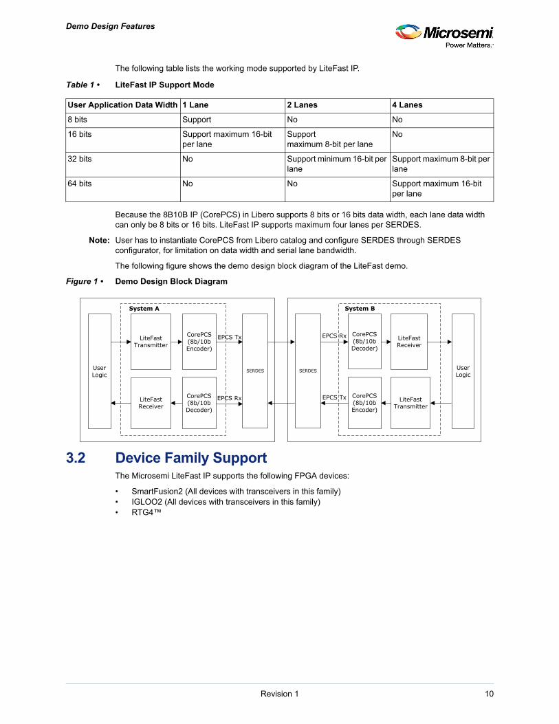
The following table lists the working mode supported by LiteFast IP.
Because the 8B10B IP (CorePCS) in Libero supports 8 bits or 16 bits data width, each lane data width can only be 8 bits or 16 bits. LiteFast IP supports maximum four lanes per SERDES.
Note: User has to instantiate CorePCS from Libero catalog and configure SERDES through SERDES configurator, for limitation on data width and serial lane bandwidth.
The following figure shows the demo design block diagram of the LiteFast demo.
Figure 1 • Demo Design Block Diagram
3.2 Device Family SupportThe Microsemi LiteFast IP supports the following FPGA devices:
• SmartFusion2 (All devices with transceivers in this family)• IGLOO2 (All devices with transceivers in this family)• RTG4™
Table 1 • LiteFast IP Support Mode
User Application Data Width 1 Lane 2 Lanes 4 Lanes
8 bits Support No No
16 bits Support maximum 16-bit per lane
Supportmaximum 8-bit per lane
No
32 bits No Support minimum 16-bit per lane
Support maximum 8-bit per lane
64 bits No No Support maximum 16-bit per lane
LiteFast Transmitter
LiteFast Receiver
SERDES User Logic
LiteFast Transmitter
LiteFast Receiver
SERDES User Logic
System A System B
CorePCS(8b/10b Decoder)
CorePCS(8b/10b Encoder)
CorePCS(8b/10b Decoder)
CorePCS(8b/10b Encoder)
EPCS Tx
EPCS Rx
EPCS Rx
EPCS Tx
Revision 1 10

Demo Design Features
3.3 Hardware DesignThe hardware design for the implementation includes a LiteFast transmitter and LiteFast receiver blocksconnected to the SmartFusion2 SERDES. UART block communicates with the GUI to send data andreceive control signals. The top-level Smart Design diagram for the design is shown in Figure 2.
Figure 2 • LiteFast Smart Design Top-Level Diagram
3.3.1 CorePCS The CorePCS supports programmable 8B10B encoding/decoding. This Core can be configured as atransmitter, receiver, or both transmitter and receiver. Word alignment support is included in receiver. TheCore can be configured to support 10-bit or 20-bit external physical coding sublayer (EPCS) data. Referto CorePCS v3.3 Handbook for more information on CorePCS block.
Revision 1 11

Demo Design Features
3.4 Block Descriptions
3.4.1 LiteFast TransmitterThe LiteFast transmitter block contains a counter to generate data, LiteFast IP in transmitter mode,CorePCS block configured in transmitter only mode, and transmitter interface for SERDES. Figure 3shows LiteFast smart design transmitter block.
Figure 3 • LiteFast Transmitter Smart Design
3.4.1.1 Counter The counter block contains a 16-bit counter that transmits incremental data, each clock cycle.
3.4.1.2 LiteFast IP in Transmitter ModeThe Lite Fast IP is configured in transmitter only mode. The IP can be configured from IP’s configuratorwindow, as shown in Figure 4. The g_DATA_WID indicates the data width, g_LANE_NUM indicates thenumber of lanes to be configured. LiteFast_Mode contains the drop down in which Transmitter Onlymode needs to be selected. For exact number of lane and data width choice, refer Table 1 on page 10.
Figure 4 • LiteFast IP Transmitter Configurator
3.4.1.3 CorePCS TransmitterThe CorePCS transmitter block multiplexes the control and data inputs on EPCS_TX_DATA. TheCorePCS uses running disparity technique for 8B/10B encoding. The CorePCS output transmit interfaceis connected to SERDES EPCS transmit interface.
Revision 1 12
Demo Design Features
3.4.1.4 EPCS Transmit InterfaceThe EPCS transmit interface block is a fabric interface that synchronizes data between SERDES blockand fabric modules.
It receives data from the fabric modules and transmits onto the SERDES.
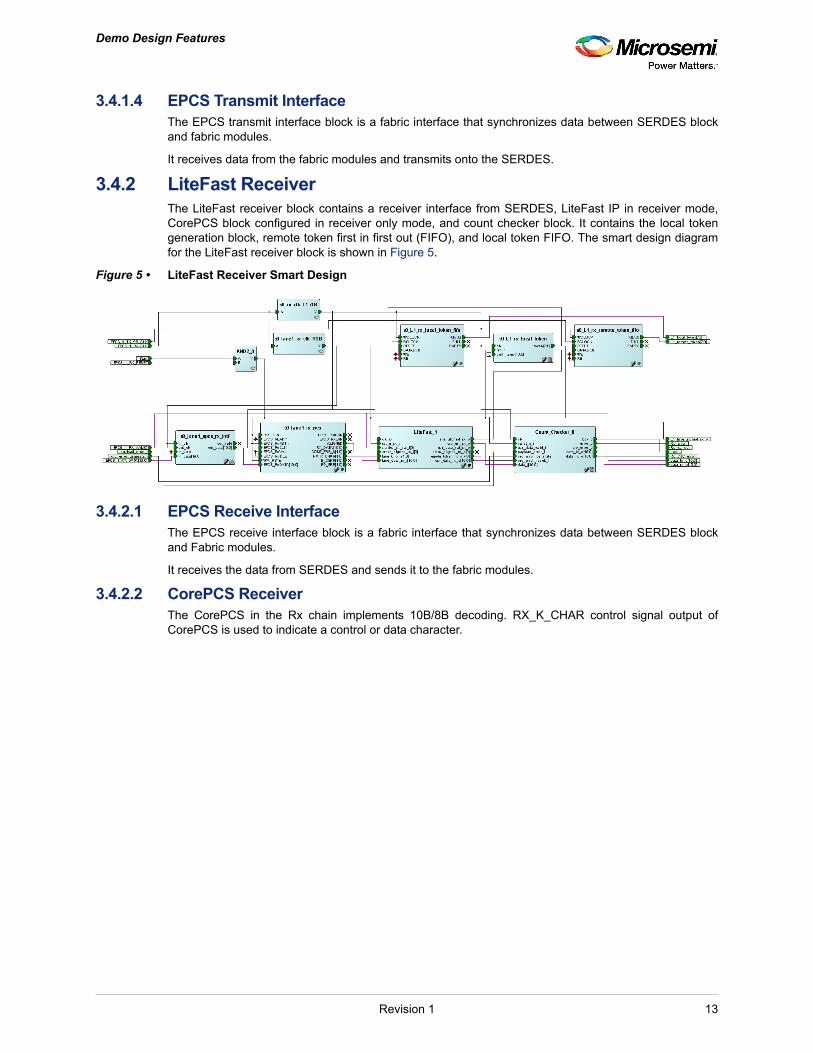
3.4.2 LiteFast ReceiverThe LiteFast receiver block contains a receiver interface from SERDES, LiteFast IP in receiver mode,CorePCS block configured in receiver only mode, and count checker block. It contains the local tokengeneration block, remote token first in first out (FIFO), and local token FIFO. The smart design diagramfor the LiteFast receiver block is shown in Figure 5.
Figure 5 • LiteFast Receiver Smart Design
3.4.2.1 EPCS Receive InterfaceThe EPCS receive interface block is a fabric interface that synchronizes data between SERDES blockand Fabric modules.
It receives the data from SERDES and sends it to the fabric modules.
3.4.2.2 CorePCS ReceiverThe CorePCS in the Rx chain implements 10B/8B decoding. RX_K_CHAR control signal output ofCorePCS is used to indicate a control or data character.
Revision 1 13
Demo Design Features
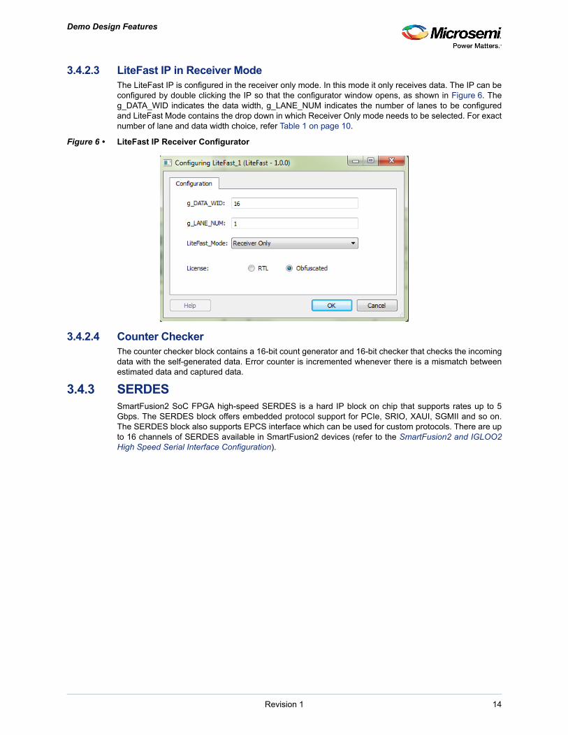
3.4.2.3 LiteFast IP in Receiver ModeThe LiteFast IP is configured in the receiver only mode. In this mode it only receives data. The IP can beconfigured by double clicking the IP so that the configurator window opens, as shown in Figure 6. Theg_DATA_WID indicates the data width, g_LANE_NUM indicates the number of lanes to be configuredand LiteFast Mode contains the drop down in which Receiver Only mode needs to be selected. For exactnumber of lane and data width choice, refer Table 1 on page 10.
Figure 6 • LiteFast IP Receiver Configurator
3.4.2.4 Counter CheckerThe counter checker block contains a 16-bit count generator and 16-bit checker that checks the incomingdata with the self-generated data. Error counter is incremented whenever there is a mismatch betweenestimated data and captured data.
3.4.3 SERDESSmartFusion2 SoC FPGA high-speed SERDES is a hard IP block on chip that supports rates up to 5Gbps. The SERDES block offers embedded protocol support for PCIe, SRIO, XAUI, SGMII and so on.The SERDES block also supports EPCS interface which can be used for custom protocols. There are upto 16 channels of SERDES available in SmartFusion2 devices (refer to the SmartFusion2 and IGLOO2High Speed Serial Interface Configuration).
Revision 1 14

Demo Design Features
In this demo design, the SERDES_IF_2 block is configured for EPCS modes on Lanex (Lanex can beLane1 or Lane2), with 20-bit parallel interface on both transmit and receive side, and external referenceclock from on board Oscillator. The configurator window for SERDES in the smart design is shown inFigure 7.
Figure 7 • SERDES Configurator window
3.4.3.1 Reference Clock SourceFor the given demo, when line speed is working at 2.5 Gbps, the reference Clock to SERDES is 125 MHzand it is given from differential pads (REFCLK1P and REFCLK1N). In SmartFusion2 Security EvaluationKit, the REFCLK1 differential pads are driven from 125 MHz on board Oscillator.
3.4.4 UARTThe UART block contains the CoreUART and FabUART modules. The FabUART module is the wrapperinterface that sends/receives commands and data to the GUI through CoreUART block. Refer toCoreUART v5.4 Handbook for more information on the CoreUART block.
Revision 1 15

Validating the Design on SmartFusion2 Security Evaluation Kit
4 Validating the Design on SmartFusion2 Security Evaluation Kit
4.1 RequirementsThe following are the hardware requirements to run the demo:
4.2 Design Files Directory StructureThe demo design files are available for download from the following path in the Microsemi website:
• For Lane1: http://soc.microsemi.com/download/rsc/?f=LiteFast_Demo_Lane1
• For Lane2: http://soc.microsemi.com/download/rsc/?f=LiteFast_Demo_Lane2
The following figure shows the top-level structure of the design files. Which are delivered along with thisdemo guide:
Figure 8 • Design Structure
Note: Lanex can be Lane1 or Lane2.
4.3 Setting the BoardThe following steps describe how to set the board for demo:
1. SmartFusion2 090T device consists one SERDES with four lanes. Lane 1 and Lane 2 can be used for external loopback testing on the SmartFusion2 Security Evaluation Kit board. Lane 1 is a PCB trace loopback on board where as Lane 2 is external SMA loopback
2. A pair of SMA-SMA cables are required to loopback SERDES TXP_2 to RXP_2 and TXN_2 to RXN_2, as shown in Figure 10 on page 17. The FlashPro4 needs to be connected to the JTAG header on the board.
Table 2 • Hardware Requirements
Description Quantity
SmartFusion2 Security Evaluation Kit One
FlashPro4 Programmer One
SMA M to SMA M loopback cables Two (required if it is Lane 2 demo)
Mini to Micro USB cable Two
STAPL/PDB file Included with project
GUI Software Included with project
Libero 11.7.1.11(11.7 SP1)
Revision 1 16

Validating the Design on SmartFusion2 Security Evaluation Kit
3. Connect the micro-USB to USB-A cable to the board, as shown in Figure 10. The USB-A connector needs to be connected to the computer. For more information on SmartFusion2 Security Evaluation Kit board refer to the UG0541: SmartFusion2 SoC FPGA Evaluation Kit User Guide.
Figure 9 • SmartFusion2 SoC FPGA Evaluation Kit Board Overview
Revision 1 17

Validating the Design on SmartFusion2 Security Evaluation Kit
Figure 10 • Board Setup
4. Install USB-UART drivers. USB-UART driver files - FT232R are available on Microsemi website.
4.4 Programming the DeviceThe following steps helps in programming the device:
1. Download the design files: • For Lane1:
http://soc.microsemi.com/download/rsc/?f=LiteFast_Demo_Lane1 • For Lane2:
http://soc.microsemi.com/download/rsc/?f=LiteFast_Demo_Lane2 Programming file (STAPL/PDB) is located in the Programming_Files folder.
2. Connect the Flashpro4 programmer to the SmartFusion2 Evaluation Kit board.3. Open FlashPro v11.7 SP1 (installed as part of the Libero IDE).4. Click New Project in FlashPro.
Revision 1 18

Validating the Design on SmartFusion2 Security Evaluation Kit
5. Enter the project name as LiteFast_Demo in the New Project window.
Figure 11 • New Project Window
If necessary, change the default location in the Project Location.
6. Select Single Device Programming mode.7. Click OK. The FlashPro GUI window is displayed. The Programmer List Window updates with
programmer information.
Figure 12 • FlashPro GUI Window
After the project is connected the program is ready to load the STAPL/PDB file downloaded.
8. Click Configure Device. The Single Device Configuration window is displayed in FlashPro.9. Click Browse to find the programming file.10. On the Load Existing Programming File window, select the required programming file and click
Open.
Revision 1 19

Validating the Design on SmartFusion2 Security Evaluation Kit
11. The Single Device Configuration window updates the programming file information and the actions available with the programming file in the Action list box (see Figure 13).
Figure 13 • Single Device Configuration Window
Note: Microsemi recommends using the default settings.
12. After loading the programming file, select Program.Click Procedures... (see Figure 14).
Figure 14 • Action List Window
Revision 1 20
Validating the Design on SmartFusion2 Security Evaluation Kit
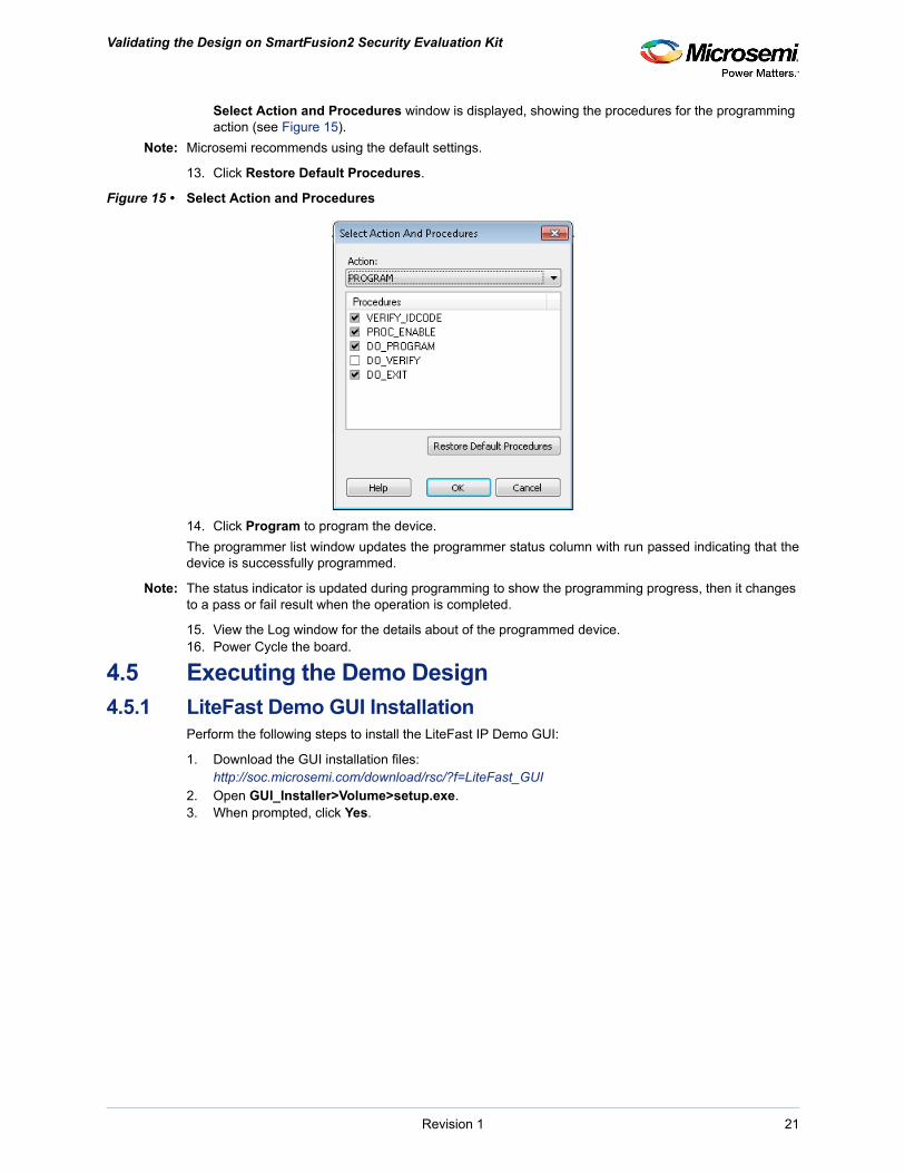
Select Action and Procedures window is displayed, showing the procedures for the programming action (see Figure 15).
Note: Microsemi recommends using the default settings.
13. Click Restore Default Procedures.
Figure 15 • Select Action and Procedures
14. Click Program to program the device.
The programmer list window updates the programmer status column with run passed indicating that thedevice is successfully programmed.
Note: The status indicator is updated during programming to show the programming progress, then it changes to a pass or fail result when the operation is completed.
15. View the Log window for the details about of the programmed device. 16. Power Cycle the board.
4.5 Executing the Demo Design
4.5.1 LiteFast Demo GUI InstallationPerform the following steps to install the LiteFast IP Demo GUI:
1. Download the GUI installation files:http://soc.microsemi.com/download/rsc/?f=LiteFast_GUI
2. Open GUI_Installer>Volume>setup.exe.3. When prompted, click Yes.
Revision 1 21
Validating the Design on SmartFusion2 Security Evaluation Kit
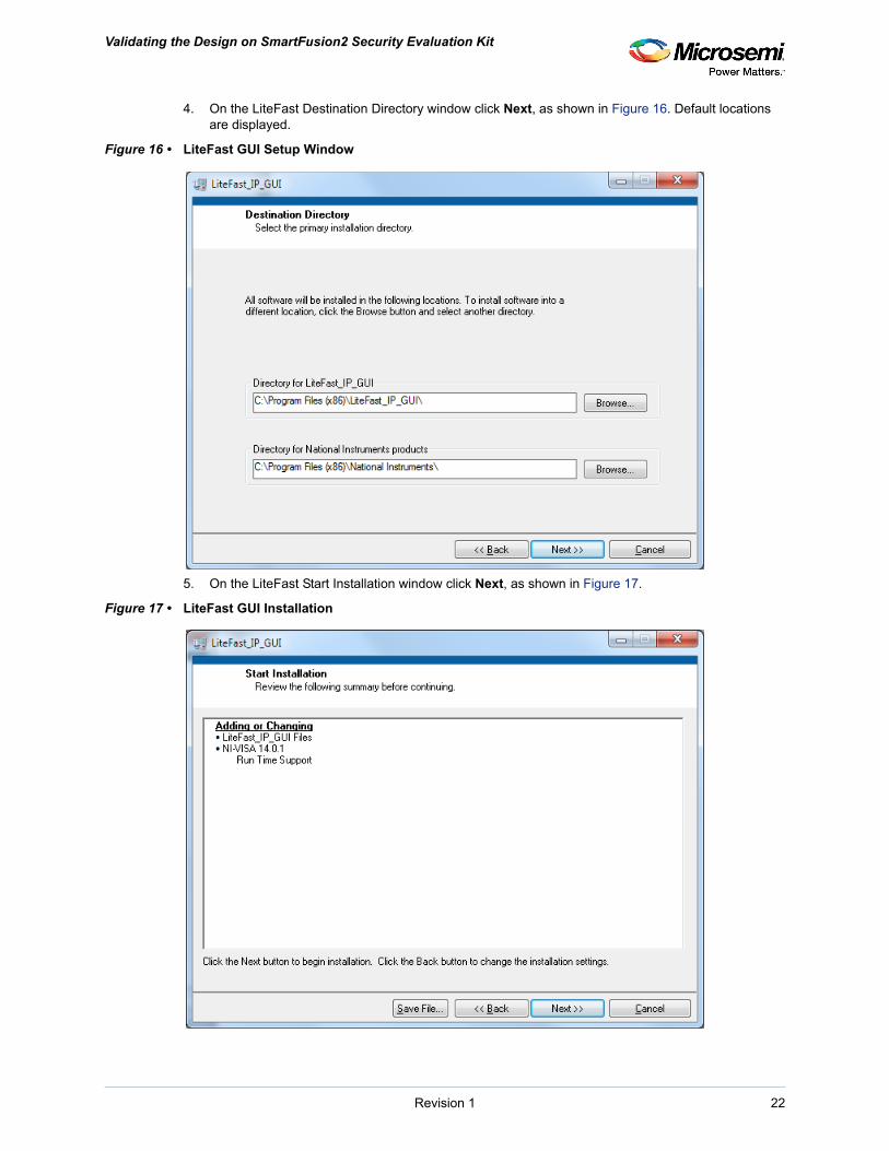
4. On the LiteFast Destination Directory window click Next, as shown in Figure 16. Default locations are displayed.
Figure 16 • LiteFast GUI Setup Window
5. On the LiteFast Start Installation window click Next, as shown in Figure 17.
Figure 17 • LiteFast GUI Installation
Revision 1 22

Validating the Design on SmartFusion2 Security Evaluation Kit
A progress bar appears which shows the progress of installation, as shown in Figure 18. Wait for the installation to complete It may take few minutes.
Figure 18 • LiteFast GUI Setup Progress Bar
6. If the installation is successful, Installation Complete message appears. Click Finish.Restart computer before using the installed GUI.
Note: The GUI given along with this demo design is applicable only for this demo design.
4.5.2 LiteFast Demo GUI Description and Usage1. Open Programs>LiteFast_IP_Demo.2. The LiteFast GUI window appears, as shown in Figure 19.
Figure 19 • LiteFast GUI Window
Revision 1 23

Validating the Design on SmartFusion2 Security Evaluation Kit
LiteFast GUI interface description is as follows:
• The drop down menu for ports gives the list of serial ports available on the host PC.• The list of serial ports differs for host PC so check the correct port that works.
Note: Default settings for the design are 9600 Baud, No flow control, 1 stop, and no parity.
• After opening the GUI, it auto detects the COM port connected to the device and establishes the communication with board. If there is any issue when connecting the host PC with board, connection can be done manually by selecting the appropriate COM port from drop down list and click connect.
• Status signals indicate the complete system operation.• If Host Connection is crossed-red, it means that the GUI failed to open a COM port. It turns
green when the GUI software is able to open the selected COM port on the host PC.• Serial Link is an indicator of the transmission link for the serial LiteFast data. If the link is up
and running, Serial Link turns green. It turns crossed-red if the link goes down.• Rx Lock is receiver lock. Rx Lock goes green, when the receiver starts receiving valid and
error free data. It means that the receiver has locked to the count sequences and the subsequent transmitted sequences can be successfully received.
• Payload Error indicates any errors received. When Payload Error goes red, the receiver finds a corrupted packet or detects any error in the received counter sequences.
• CRC Error indicates any CRC Errors. When CRC Error goes red, the CRC checker in receiver finds a corrupted packet or detects any loss of sequence in the received counter sequences.
• RX Words: Shows the number of received data words. This number rolls over after 65535 words.
• TX Words: Shows the number of transmitted data words. This number rolls over after 65535 words.
• Error Counter: It indicates the packet loss and rolls over after 65535 words. Note: Error counter may not exactly co-relate to TX words and RX words due to the rollover.
• Payload Error Slider: It is used to introduce errors in the transmission for debug purposes. By enabling this slider it injects the error in the transmitted count sequence which as a result, increments the Error Count display and Payload Error turns Red
• CRC Error Slider: It is used to introduce CRC errors in the transmission for debug purposes. By enabling this slider it injects the CRC error in the transmitted count sequence which as a result, CRC Error indicator turns Red
• Clicking Start: Starts the LiteFast demo. The Counter starts transmitting count data which is sent over serial transmit link. It is then received by the receiver and checked for any errors. The status at any time can be monitored using the status signals in the GUI.
• Clicking Stop: Stops the LiteFast Demo.• Click Exit: Exits the GUI.
Revision 1 24

Validating the Design on SmartFusion2 Security Evaluation Kit
Figure 20 shows how the GUI looks like during an error free operation of the LiteFast demo system.
Figure 20 • Connected LiteFast GUI
Figure 21 shows how the GUI looks like during payload error injection of the LiteFast demo system.
Figure 21 • GUI with Payload Error Injection
Revision 1 25

Validating the Design on SmartFusion2 Security Evaluation Kit
Figure 22 shows how the GUI looks like during CRC error injection of the LiteFast demo system.
Figure 22 • GUI with CRC Error Injection
Revision 1 26
Using LiteFast in Customer Application
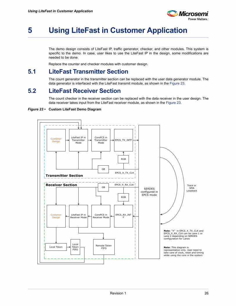
5 Using LiteFast in Customer Application
The demo design consists of LiteFast IP, traffic generator, checker, and other modules. This system isspecific to the demo. In case, user likes to use the LiteFast IP in the design, some modifications areneeded to be done.
Replace the counter and checker modules with customer design.
5.1 LiteFast Transmitter SectionThe count generator in the transmitter section can be replaced with the user data generator module. Thedata generator is interfaced with the LiteFast transmit module, as shown in the Figure 23.
5.2 LiteFast Receiver SectionThe count checker in the receiver section can be replaced with the data receiver in the user design. Thedata receiver takes input from the LiteFast receiver module, as shown in the Figure 23.
Figure 23 • Custom LiteFast Demo Diagram
Revision 1 26
Using LiteFast in Customer Application
5.3 Guidelines for Libero Design FlowFollowing are the guidelines for Libero design flow:
1. Create the design using smart design in the Libero v11.7 SP1.2. Add the LiteFast IP from the IP catalogue.3. Configure the transmitter and receiver sections, as per system requirements.4. Go through the synthesis and check for any warnings.5. Adjust the DELAY value of the delay line module in EPCS RX module to avoid any hold violations.6. Give proper LiteFast TX and RX clock constraints.7. Proper care for clock crossing needs to be taken for local and remote token handling. 8. Complete the implementation and generate the bit stream.9. Program the device.10. Execute the design and check the functionality.
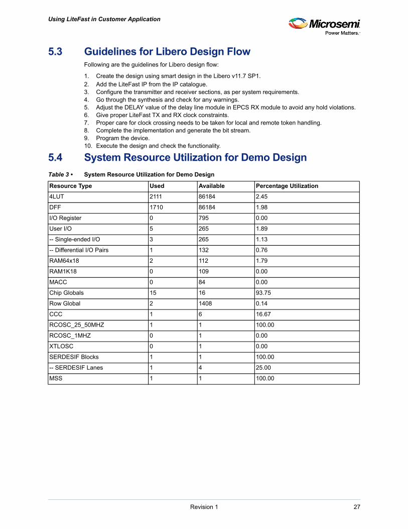
5.4 System Resource Utilization for Demo Design
Table 3 • System Resource Utilization for Demo Design
Resource Type Used Available Percentage Utilization
4LUT 2111 86184 2.45
DFF 1710 86184 1.98
I/O Register 0 795 0.00
User I/O 5 265 1.89
-- Single-ended I/O 3 265 1.13
-- Differential I/O Pairs 1 132 0.76
RAM64x18 2 112 1.79
RAM1K18 0 109 0.00
MACC 0 84 0.00
Chip Globals 15 16 93.75
Row Global 2 1408 0.14
CCC 1 6 16.67
RCOSC_25_50MHZ 1 1 100.00
RCOSC_1MHZ 0 1 0.00
XTLOSC 0 1 0.00
SERDESIF Blocks 1 1 100.00
-- SERDESIF Lanes 1 4 25.00
MSS 1 1 100.00
Revision 1 27

Product Support
6 Product Support
Microsemi SoC Products Group backs its products with various support services, including CustomerService, Customer Technical Support Center, a website, electronic mail, and worldwide sales offices.This appendix contains information about contacting Microsemi SoC Products Group and using thesesupport services.
6.1 Customer ServiceContact Customer Service for non-technical product support, such as product pricing, product upgrades,update information, order status, and authorization.
From North America, call 800.262.1060From the rest of the world, call 650.318.4460Fax, from anywhere in the world, 408.643.6913
6.2 Customer Technical Support CenterMicrosemi SoC Products Group staffs its Customer Technical Support Center with highly skilledengineers who can help answer your hardware, software, and design questions about Microsemi SoCProducts. The Customer Technical Support Center spends a great deal of time creating applicationnotes, answers to common design cycle questions, documentation of known issues, and various FAQs.So, before you contact us, please visit our online resources. It is very likely we have already answeredyour questions.
6.3 Technical SupportFor Microsemi SoC Products Support, visit http://www.microsemi.com/products/fpga-soc/design-support/fpga-soc-support.
6.4 WebsiteYou can browse a variety of technical and non-technical information on the Microsemi SoC ProductsGroup home page, at http://www.microsemi.com/products/fpga-soc/fpga-and-soc.
6.5 Contacting the Customer Technical Support CenterHighly skilled engineers staff the Technical Support Center. The Technical Support Center can becontacted by email or through the Microsemi SoC Products Group website.
6.5.1 EmailYou can communicate your technical questions to our email address and receive answers back by email,fax, or phone. Also, if you have design problems, you can email your design files to receive assistance.We constantly monitor the email account throughout the day. When sending your request to us, pleasebe sure to include your full name, company name, and your contact information for efficient processing ofyour request.
The technical support email address is [email protected].
6.5.2 My CasesMicrosemi SoC Products Group customers may submit and track technical cases online by going to MyCases.
6.5.3 Outside the U.S.Customers needing assistance outside the US time zones can either contact technical support via email([email protected]) or contact a local sales office. Visit About Us for sales office listings andcorporate contacts.
Revision 1 28

Product Support
6.6 ITAR Technical SupportFor technical support on RH and RT FPGAs that are regulated by International Traffic in ArmsRegulations (ITAR), contact us via [email protected]. Alternatively, within My Cases, select Yesin the ITAR drop-down list. For a complete list of ITAR-regulated Microsemi FPGAs, visit the ITAR webpage.
Revision 1 29