diamond security system in a museum with loud 60db siren1
TRANSCRIPT

Diamond Security System In Museum
CHAPTER 1
INTRODUCTION
1.1 OVERVIEW:
The overview of this project is to design effective security alarm system that can
monitor the diamond in a museum using LDR sensors.
1.2 PURPOSE:
The purpose of the current work is to study and analyse the system which is useful in
real time situation whenever somebody picks the diamond, the light of LED falls on the LDR
and it triggers 60dB is connected to this SCR and gets activated in triggered conditions.
1.3 SCOPE:
Current work focuses on how to trigger (activating) 60dB siren when an unauthorised
person picks up the diamond in a museum.
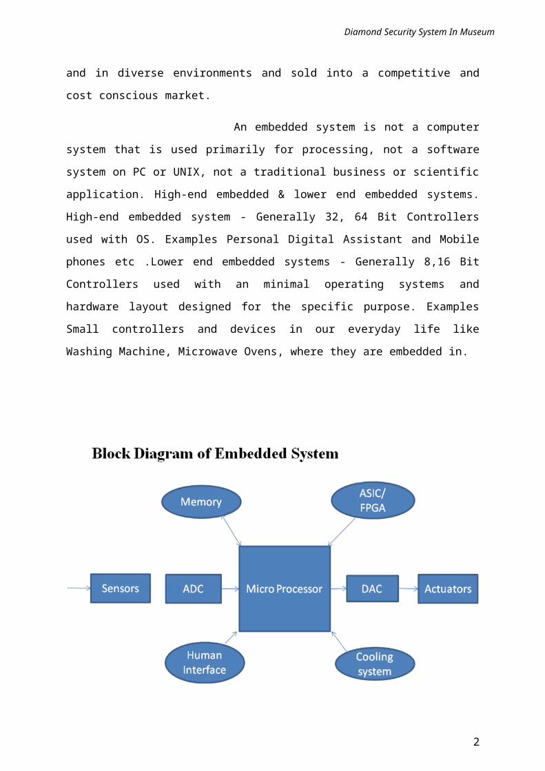
INTRODUCTION TO EMBEDDED SYSTEMS
EMBEDDED SYSTEM:
Embedded System is a combination of hardware and software used to achieve a
single specific task. An embedded system is a microcontroller-based, software driven,
reliable, real-time control system, autonomous, or human or network interactive, operating on
diverse physical variables and in diverse environments and sold into a competitive and cost
conscious market.
An embedded system is not a computer system that is used primarily for
processing, not a software system on PC or UNIX, not a traditional business or scientific
application. High-end embedded & lower end embedded systems. High-end embedded
system - Generally 32, 64 Bit Controllers used with OS. Examples Personal Digital Assistant
and Mobile phones etc .Lower end embedded systems - Generally 8,16 Bit Controllers used
with an minimal operating systems and hardware layout designed for the specific purpose.
Examples Small controllers and devices in our everyday life like Washing Machine,
Microwave Ovens, where they are embedded in.
1
Diamond Security System In Museum
Characteristics of Embedded System:
• An embedded system is any computer system hidden inside a product other than a
computer
• There will encounter a number of difficulties when writing embedded system
software in addition to those we encounter when we write applications
– Throughput – Our system may need to handle a lot of data in a short period of time.
– Response–Our system may need to react to events quickly
– Testability–Setting up equipment to test embedded software can be difficult
– Debugability–Without a screen or a keyboard, finding out what the software is doing
wrong (other than not working) is a troublesome problem
– Reliability – embedded systems must be able to handle any situation without human
intervention
2

Diamond Security System In Museum
– Memory space – Memory is limited on embedded systems, and you must make the
software and the data fit into whatever memory exists
– Program installation – you will need special tools to get your software into embedded
systems
– Power consumption – Portable systems must run on battery power, and the software
in these systems must conserve power
– Processor hogs – computing that requires large amounts of CPU time can complicate
the response problem
– Cost – Reducing the cost of the hardware is a concern in many embedded system
projects; software often operates on hardware that is barely adequate for the job.
• Embedded systems have a microprocessor/ microcontroller and a memory. Some
have a serial port or a network connection. They usually do not have keyboards, screens or
disk drives.
Applications:
1. Military and aerospace embedded software applications
2. Communication Applications
3. Industrial automation and process control software.
3

Diamond Security System In Museum
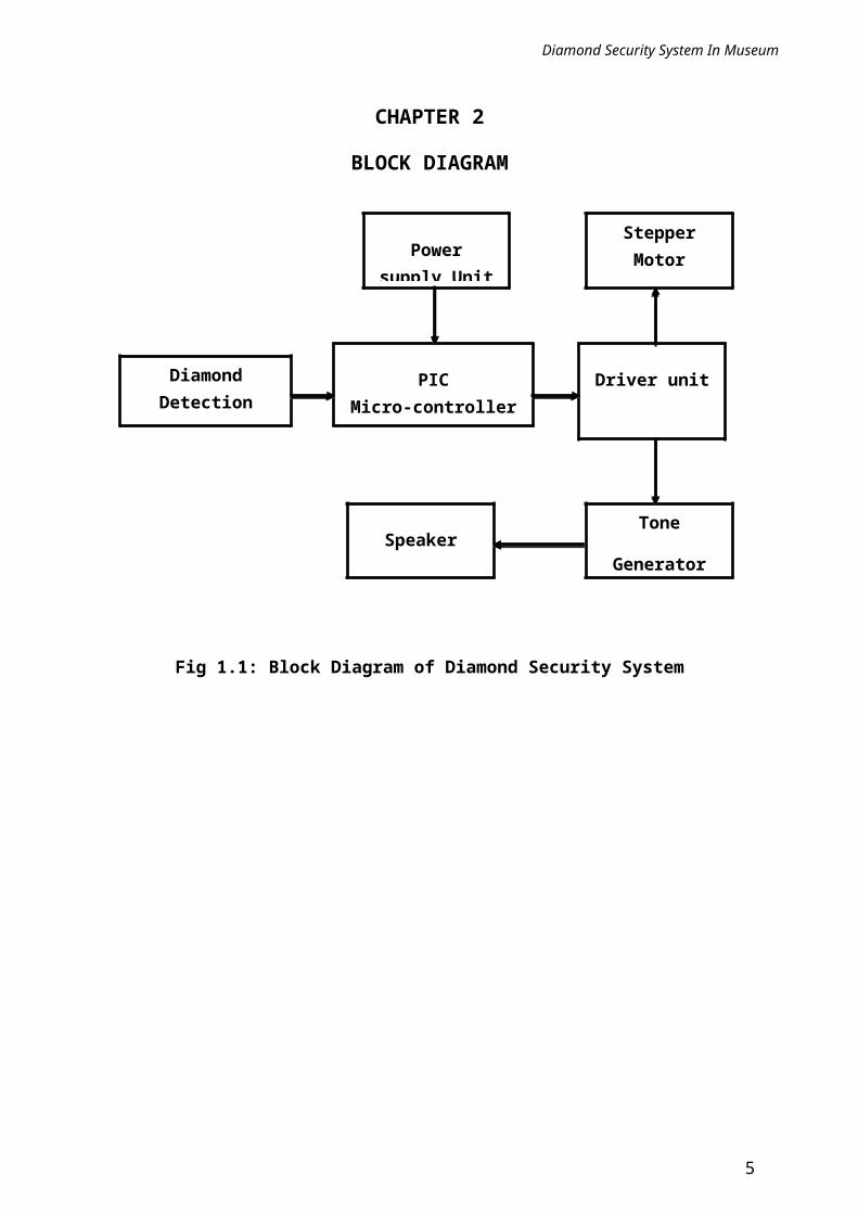
CHAPTER 2
BLOCK DIAGRAM
Fig 1.1: Block Diagram of Diamond Security System
4
Power supply Unit
StepperMotor
PICMicro-controller
DiamondDetection sensor
Driver unit
SpeakerTone
Generator
Diamond Security System In Museum
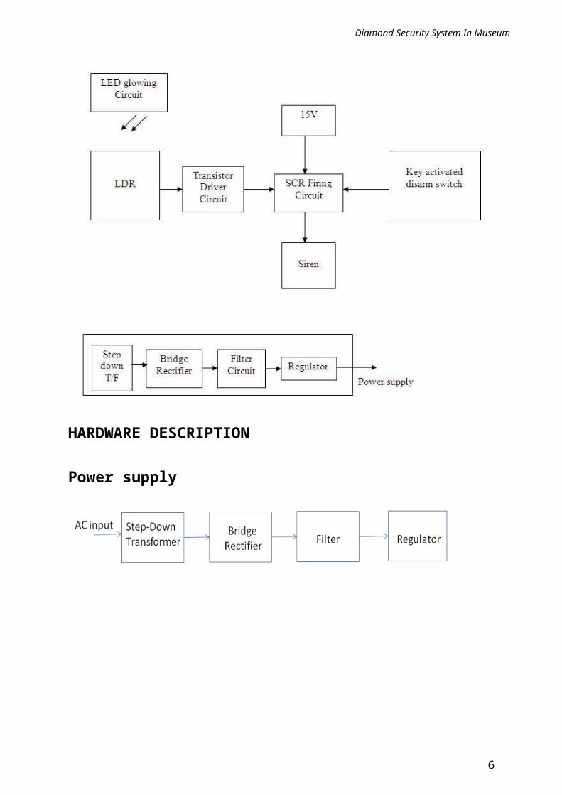
HARDWARE DESCRIPTION
Power supply
5
Diamond Security System In Museum
Circuit Diagram
Power supply unit consists of following units
i) Step down transformer
ii) Rectifier unit
iii) Flter
iv) Regulator unit
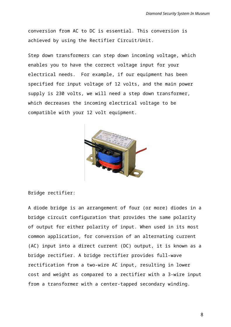
STEPDOWN TRANSFORMER:
The Step down Transformer is used to step down the main supply voltage from 230V
AC to lower value. This 230 AC voltage cannot be used directly, thus it is stepped down. The
Transformer consists of primary and secondary coils. To reduce or step down the voltage, the
transformer is designed to contain less number of turns in its secondary core. The output from
the secondary coil is also AC waveform. Thus the conversion from AC to DC is essential.
This conversion is achieved by using the Rectifier Circuit/Unit.
Step down transformers can step down incoming voltage, which enables you to have the
correct voltage input for your electrical needs. For example, if our equipment has been
specified for input voltage of 12 volts, and the main power supply is 230 volts, we will need a
6
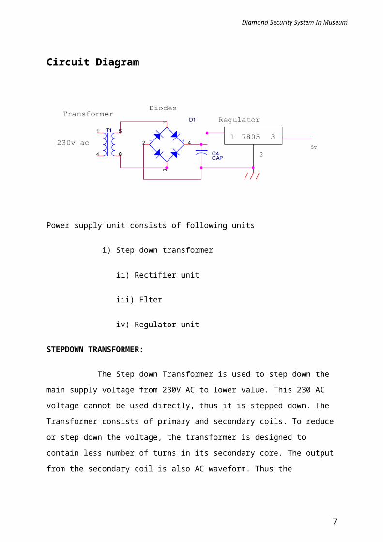
Diamond Security System In Museum
step down transformer, which decreases the incoming electrical voltage to be compatible with
your 12 volt equipment.
Bridge rectifier:
A diode bridge is an arrangement of four (or more) diodes in a bridge circuit configuration
that provides the same polarity of output for either polarity of input. When used in its most
common application, for conversion of an alternating current (AC) input into a direct current
(DC) output, it is known as a bridge rectifier. A bridge rectifier provides full-wave
rectification from a two-wire AC input, resulting in lower cost and weight as compared to a
rectifier with a 3-wire input from a transformer with a center-tapped secondary winding.
According to the conventional model of current flow (originally established by Benjamin
Franklin and still followed by most engineers today[2]), current is assumed to flow through
electrical conductors from the positive to the negative pole.
In actuality, free electrons in a conductor nearly always flow from the negative to the positive
pole. In the vast majority of applications, however, the actual direction of current flow is
irrelevant. Therefore, in the discussion below the conventional model is retained.
In the diagrams below, when the input connected to the left corner of the diamond is positive,
and the input connected to the right corner is negative, current flows from the upper supply
terminal to the right along the red (positive) path to the output, and returns to the lower
supply terminal via the blue (negative) path.
7
Diamond Security System In Museum
In each case, the upper right output remains positive and lower right output negative. Since
this is true whether the input is AC or DC, this circuit not only produces a DC output from an
AC input, it can also provide what is sometimes called "reverse polarity protection". That is,
it permits normal functioning of DC-powered equipment when batteries have been installed
backwards, or when the leads (wires) from a DC power source have been reversed, and
protects the equipment from potential damage caused by reverse polarity.
FILTER:
Capacitors are used as filter. The ripples from the DC voltage are removed and pure
DC voltage is obtained. And also these capacitors are used to reduce the harmonics of the
input voltage. The primary action performed by capacitor is charging and discharging. It
charges in positive half cycle of the AC voltage and it will discharge in negative half cycle.
So it allows only AC voltage and does not allow the DC voltage. This filter is fixed before
the regulator. Thus the output is free from ripples.
There are two types of filters. They are
1. Low pass filter
2. High pass filter
Voltage Regulator:
8

Diamond Security System In Museum
A voltage regulator is designed to automatically maintain a constant voltage level. A voltage
regulator may be a simple "feed-forward" design or may include negative feedback control
loops. It may use an electromechanical mechanism, or electronic components. Depending on
the design, it may be used to regulate one or more AC or DC voltages.
Electronic voltage regulators are found in devices such as computer power supplies where
they stabilize the DC voltages used by the processor and other elements. In automobile
alternators and central power station generator plants, voltage regulators control the output of
the plant. In an electric power distribution system, voltage regulators may be installed at a
substation or along distribution lines so that all customers receive steady voltage independent
of how much power is drawn from the line.
7805 is a voltage regulator integrated circuit. It is a member of 78xx series of fixed linear
voltage regulator ICs. The voltage source in a circuit may have fluctuations and would not
give the fixed voltage output. The voltage regulator IC maintains the output voltage at a
constant value. The xx in 78xx indicates the fixed output voltage it is designed to provide.
7805 provides +5V regulated power supply. Capacitors of suitable values can be connected at
input and output pins depending upon the respective voltage levels.
Pin Diagram:
9
Diamond Security System In Museum
Pin Description:
Pin No Function Name
1 Input voltage (5V-18V) Input
2 Ground (0V) Ground
3 Regulated output; 5V (4.8V-5.2V) Output
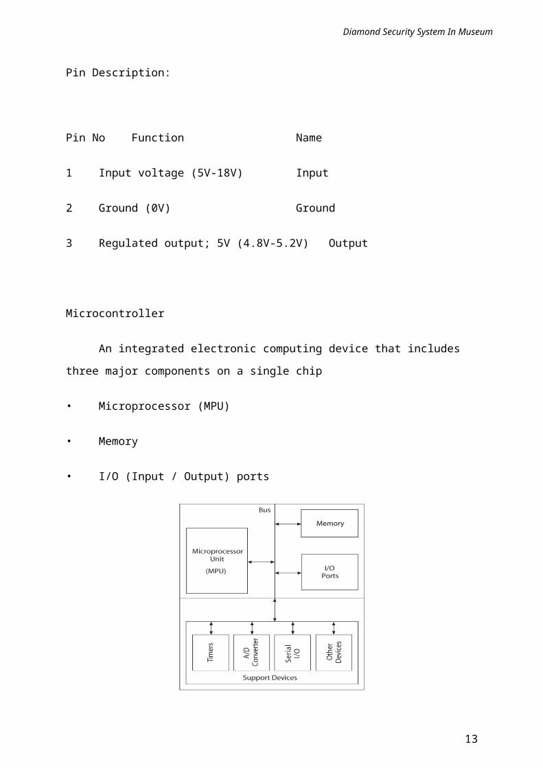
Microcontroller
An integrated electronic computing device that includes three major components on a
single chip
• Microprocessor (MPU)
• Memory
• I/O (Input / Output) ports
MCU Block Diagram
10
Diamond Security System In Museum
PIC CONTROLLER:
PIC is a family of modified Harvard architecture microcontrollers made by Microchip
Technology, derived from the PIC1650[1][2][3] originally developed by General Instrument's
Microelectronics Division. The name PIC initially referred to "Peripheral Interface
Controller".
PICs are popular with both industrial developers and hobbyists alike due to their low cost,
wide availability, large user base, extensive collection of application notes, availability of low
cost or free development tools, and serial programming (and re-programming with flash
memory) capability. They are also commonly used in educational programming as they often
come with the easy to use 'pic logicator' software.
Advantages
• Small instruction set to learn
• RISC architecture
• Built in oscillator with selectable speeds
• Easy entry level, in circuit programming plus in circuit debugging PIC Kit units
available for less .
• Inexpensive microcontrollers
• Wide range of interfaces including I²C, SPI, USB, USART, A/D, programmable
comparators, PWM, LIN, CAN, PSP, and Ethernet[8]
• Availability of processors in DIL package makes them easy to handle for hobby use.
FEATURES OF PIC16F877A CONTROLLER:
• High-performance RISC CPU.
• Only 35 single word instructions to learn.
• All single cycle instructions except for program branches which are two cycle.
11

Diamond Security System In Museum
• Operating speed: DC - 20 MHz clock input DC - 200 ns instruction cycle.
• Up to 8K x 14 words of FLASH Program Memory, Up to 368 x 8 bytes of Data
Memory (RAM) Up to 256 x 8 bytes of EEPROM data memory.
• Pin out compatible to the PIC16C73B/74B/76/77
• Interrupt capability (up to 14 sources)
• Eight level deep hardware stack
• Direct, indirect and relative addressing modes.
• Power-on Reset (POR).
• Power-up Timer (PWRT) and Oscillator Start-up Timer (OST).
• Watchdog Timer (WDT) with its own on-chip RC oscillator for reliable operation.
• Programmable code-protection.
• Power saving SLEEP mode.
• Selectable oscillator options.
• Low-power, high-speed CMOS FLASH/EEPROM technology.
• Fully static design.
• In-Circuit Serial Programming (ICSP) .
• Single 5V In-Circuit Serial Programming capability.
• In-Circuit Debugging via two pins.
• Processor read/write access to program memory.
• Wide operating voltage range: 2.0V to 5.5V.
• High Sink/Source Current: 25 mA.
12
Diamond Security System In Museum
• Commercial and Industrial temperature ranges.
• Low-power consumption.
- < 2 mA typical @ 5V, 4 MHz
- 20 A typical @ 3V, 32 kHz
- < 1 A typical standby current
PIN DIAGRAM;
PERIPHERAL FEATURES:
• Timer0: 8-bit timer/counter with 8-bit prescaler
13
Diamond Security System In Museum
• Timer1: 16-bit timer/counter with prescaler, can be incremented during sleep via external
crystal/clock
• Timer2: 8-bit timer/counter with 8-bit period register, prescaler and postscaler
• Two Capture, Compare, PWM modules
- Capture is 16-bit, max. Resolution is 12.5 ns
- Compare is 16-bit, max. Resolution is 200 ns
- PWM max. Resolution is 10-bit
• 10-bit multi-channel Analog-to-Digital converter
• Synchronous Serial Port (SSP) with SPI (Master Mode) and I2C (Master/Slave)
• Universal Synchronous Asynchronous Receiver Transmitter (USART/SCI) with 9-bit
address detection
• Parallel Slave Port (PSP) 8-bits wide, with external RD, WR and CS controls (40/44-pin
only)
• Brown-out detection circuitry for Brown-out Reset (BOR)
CMOS TECHNOLOGY:
• Low-power, high-speed Flash/EEPROM technology.
• Fully static design.
• Wide operating voltage range (2.0V to 5.5V).
• Commercial and Industrial temperature ranges.
• Low-power consumption.
14

Diamond Security System In Museum
ARCHITECTURE:
15
Diamond Security System In Museum
PIN DESCRIPTION:
OSC1/CLKI:
Oscillator crystal or external clock input. Oscillator crystal input or external clock source
input. ST buffer when configured in RC mode; otherwise CMOS. External clock source
input. Always associated with pin function OSC1 (see OSC1/CLKI, OSC2/CLKO pins).
OSC2/CLKO:
Oscillator crystal or clock output. Oscillator crystal output. Connects to The crystal or
resonator in Crystal Oscillator mode. In RC mode, OSC2 pin outputs CLKO, which has 1/4
the frequency of OSC1 and denotes the instruction cycle rate.
MCLR/VPP:
Master Clear (input) or programming voltage (output). Master Clear (Reset) input.
This pin is an active low Reset to the device. Programming voltage input.
• RA0/AN0.
• RA1/AN1.
• RA2/AN2/VREF-/CVREF.
• VREFCVREF.
• RA3/AN3/VREF+.
• VREF+.
• RA4/T0CKI/C1OUT.
• T0CKI.
• C1OUT.
16

Diamond Security System In Museum
• RA5/AN4/SS/C2OUT/SS/C2OUT.
I/O PORTS:
Some pins for these I/O ports are multiplexed with an alternate function for the peripheral
features on the device. In general, when a peripheral is enabled, that pin may not be used as a
general purpose I/O pin.
PORTA AND TRISA REGISTER:
PORTA is a 6-bit wide, bidirectional port. The corresponding data direction register is
TRISA. Setting a TRISA bit (= 1) will make the corresponding PORTA pin an input (i.e., put
the corresponding output driver in a High – Impedance mode). Clearing a TRISA bit (= 0)
will make the corresponding PORTA pin an output (i.e., put the contents of the output latch
on the selected pin). Reading the PORTA register reads the status of the pins, whereas
writing to it will write to the port latch. All write operations are read-modify-write operations.
Therefore, a write to a port implies that the port pins are read; the value is modified and then
written to the port data latch.
Pin RA4 is multiplexed with the Timer0 module clock input to become the RA4/T0CKI pin.
The RA4/T0CKI pin is a Schmitt Trigger input and an open-drain output. All other PORTA
pins have TTL input levels and full CMOS output drivers. Other PORTA pins are
multiplexed with analog inputs and the analog VREF input for both the A/D converters and
the comparators. The operation of each pin is selected by clearing/setting the appropriate
control bits in the ADCON1 and/or CMCON registers. The TRISA register controls the
direction of the port pins even when they are being used as analog inputs. The user must
ensure the bits in the TRISA register are maintained set when using them as analog inputs.
Note: On a Power-on Reset, these pins are configured as analog inputs and read as ‘0’. The
comparators are in the off (digital).
17

Diamond Security System In Museum
PORT B AND TRISB REGISTER:
PORTB is an 8-bit wide, bidirectional port. The corresponding data direction register is
TRISB. Setting a TRISB bit (= 1) will make the corresponding PORTB pin an input (i.e., put
the corresponding output driver in a High-Impedance mode). Clearing a TRISB bit (= 0) will
make the corresponding PORTB pin an output (i.e., put the contents of the output latch on the
selected pin). Three pins of PORTB are multiplexed with the In-Circuit Debugger and Low-
Voltage Programming function: RB3/PGM, RB6/PGC and RB7/PGD.
Four of the PORTB pins, RB7:RB4, have an interruption- change feature. Only pins
configured as inputs can cause this interrupt to occur (i.e., any RB7:RB4 pin configured as an
output is excluded from the interruption- change comparison). The input pins (of RB7:RB4)
are compared with the old value latched on the last read of PORTB. The “mismatch” outputs
of RB7:RB4 are OR’ed together to generate the RB port change interrupt with flag bit RBIF
(INTCON<0>).
This interrupt can wake the device from Sleep. The user, in the Interrupt Service
Routine, can clear the interrupt in the following manner:
a) Any read or write of PORTB. This will end the mismatch condition.
b) Clear flag bit RBIF.
A mismatch condition will continue to set flag bit RBIF. Reading PORTB will
end the mismatch condition and allow flag bit RBIF to be cleared. The interrupt-on-change
feature is recommended for wake-up on key depression operation and operations where
PORTB is only used for the interrupt-on-change feature. Polling of PORTB is not
recommended while using the interrupt-on- change feature. This interrupt-on-mismatch
feature, together with software configurable pull-ups on these four pins, allow easy interface
to a keypad and make it possible for wake-up on key depression.
PORTC AND TRISC REGISTER:
PORTC is an 8-bit wide, bidirectional port. The corresponding data direction register is
TRISC. Setting a TRISC bit (= 1) will make the corresponding PORTC pin an input (i.e., put
the corresponding output driver in a High- Impedance mode). Clearing a TRISC bit (= 0) will
18

Diamond Security System In Museum
make the corresponding PORTC pin an output (i.e., put the contents of the output latch on the
selected pin). PORTC is multiplexed with several peripheral functions (Table 4-5). PORTC
pins have Schmitt Trigger input buffers. When the I2C module is enabled, the PORTC<4:3>
pins can be configured with normal I2C levels, or with SMBus levels, by using the CKE bit
(SSPSTAT<6>). When enabling peripheral functions, care should be taken in defining TRIS
bits for each PORTC pin. Some peripherals override the TRIS bit to make a pin an output,
while other peripherals override the TRIS bit to make a pin an input. Since the TRIS bit
override is in effect while the peripheral is enabled, read-modify write instructions (BSF,
BCF, XORWF) with TRISC as the destination, should be avoided. The user should refer to
the corresponding peripheral section for the correct TRIS bit settings.
PORTD AND TRISD REGISTERS:
PORTD is an 8-bit port with Schmitt Trigger input buffers. Each pin is individually
configurable as an input or output. PORTD can be configured as an 8-bit wide
microprocessor port (Parallel Slave Port) by setting control bit, PSP MODE (TRISE<4>). In
this mode, the input buffers are TTL.
PORTE AND TRISE REGISTER:
PORTE has three pins (RE0/RD/AN5, RE1/WR/AN6 and RE2/CS/AN7) which are
individually configurable as inputs or outputs. These pins have Schmitt Trigger input buffers.
The PORTE pins become the I/O control inputs for the microprocessor port when bit
PSPMODE (TRISE<4>) is set. In this mode, the user must make certain that the TRISE<2:0>
bits are set and that the pins are configured as digital inputs. Also, ensure that ADCON1 is
configured for digital I/O. In this mode, the input buffers are TTL. Register 4-1 shows the
TRISE register which also controls the Parallel Slave Port operation. PORTE pins are
multiplexed with analog inputs.
When selected for analog input, these pins will read as ‘0’s. TRISE controls. The
direction of the RE pins, even when they are being used as analog inputs. The user must
make sure to keep the pins configured as inputs when using them as analog inputs.
MEMORY ORGANIZATION:
19
Diamond Security System In Museum
There are three memory blocks in each of the PIC16F87XA devices. The program memory
and data memory have separate buses so that concurrent access can occur and is detailed in
this section. The EEPROM data memory block is detailed in.
PROGRAM MEMORY ORGANIZATION:
The PIC16F87XA devices have a 13-bit program counter capable of addressing an 8K word x
14 bit program memory space. The PIC16F876A/877A devices have 8K words x 14 bits of
Flash program memory, while PIC16F873A/874A devices have 4K words x 14 bits.
Accessing a location above the physically implemented address will cause a wraparound. The
Reset vector is at 0000h and the interrupt vector is at 0004h.
The data memory is partitioned into multiple banks which contain the General
Purpose Registers and the Special Function Registers. Bits RP1 (Status<6>) and RP0
(Status<5>) are the bank select bits. Each bank extends up to 7Fh (128 bytes). The lower
locations of each bank are reserved for the Special Function Registers. Above the Special
Function Registers are General Purpose Registers, implemented as static RAM. All
implemented banks contain Special Function Registers. Some frequently used Special
Function Registers from one bank may be mirrored in another bank for code reduction and
quicker access.
TIMER0 MODULE:
The Timer0 module timer/counter has the following features:
• 8-bit timer/counter
• Readable and writable
• 8-bit software programmable prescaler
• Internal or external clock select
• Interrupt on overflow from FFh to 00h
• Edge select for external clock
20
Diamond Security System In Museum
Timer mode is selected by clearing bit T0CS (OPTION_REG<5>). In Timer mode, the
Timer0 module will increment every instruction cycle (without prescaler). If the TMR0
register is written, the increment is inhibited for the following two instruction cycles. The
user can work around this by writing an adjusted value to the TMR0 register.
TIMER0 INTERRUPT:
The TMR0 interrupt is generated when the TMR0 register overflows from FFh to 00h.
This overflow sets bit TMR0IF (INTCON<2>). The interrupt can be masked by clearing bit
TMR0IE (INTCON<5>). Bit TMR0IF must be cleared in software by the Timer0 module
Interrupt Service Routine before re-enabling this interrupt. The TMR0 interrupt cannot
awaken the processor from Sleep since the timer is shut-off during Sleep.
TIMER1 MODULE:
The Timer1 module is a 16-bit timer/counter consisting of two 8-bit registers
(TMR1H and TMR1L) which are readable and writable. The TMR1 register pair
(TMR1H:TMR1L) increments from 0000h to FFFFh and rolls over to 0000h. The TMR1
interrupt, if enabled, is generated on overflow which is latched in interrupt flag bit, TMR1IF
(PIR1<0>). This interrupt can be enabled/disabled by setting or clearing TMR1 interrupt
enable bit, TMR1IE (PIE1<0>). Timer1 can operate in one of two modes:
• As a Timer
• As a Counter
The operating mode is determined by the clock select bit, TMR1CS (T1CON<1>).
In Timer mode, Timer1 increments every instruction cycle. In Counter mode, it increments
on every rising edge of the external clock input. Timer1 can be enabled/disabled by
setting/clearing control bit, TMR1ON (T1CON<0>).Timer1 also has an internal “Reset
input”. This Reset can be generated by either of the two CCP modules. Shows the Timer1
Control register. When the
21
Diamond Security System In Museum
Timer1 oscillator is enabled (T1OSCEN is set), the RC1/T1OSI/CCP2 and
RC0/T1OSO/T1CKI pins become inputs. That is, the TRISC<1:0> value is ignored and these
pins read as ‘0’.
TIMER2 MODULE:
Timer2 is an 8-bit timer with a prescaler and a postscaler. It can be used as the PWM
time base for the PWM mode of the CCP module(s). The TMR2 register is readable and
writable and is cleared on any device Reset. The input clock (FOSC/4) has a prescale option
of 1:1, 1:4 or 1:16, selected by control bits T2CKPS1:T2CKPS0 (T2CON<1:0>). The Timer2
module has an 8-bit period register, PR2. Timer2 increments from 00h until it matches PR2
and then resets to 00h on the next increment cycle. PR2 is a readable and writable register.
The PR2 register is initialized to FFh upon Reset. The match output of TMR2 goes through a
4-bit postscaler (which gives a 1:1 to 1:16 scaling inclusive) to generate a TMR2 interrupt
(latched in flag bit, TMR2IF (PIR1<1>)). Timer2 can be shut-off by clearing control bit,
TMR2ON (T2CON<2>), to minimize power consumption.
IN-CIRCUIT DEBUGGER:
PIC16F87XA devices have a Watchdog Timer which can be shut-off only through
configuration bits. It runs off its own RC oscillator for added reliability. There are two timers
that offer necessary delays on power-up. One is the Oscillator Start-up Timer (OST),
intended to keep the chip in Reset until the crystal oscillator is stable. The other is the Power-
up Timer (PWRT), which provides a fixed delay of 72 ms (nominal) on power-up only. It is
designed to keep the part
In Reset while the power supply stabilizes. With these two timers on-chip, most applications
need no external Reset circuitry. Sleep mode is designed to offer a very low current power-
down mode. The user can wake-up from Sleep through external Reset, Watchdog Timer
wake-up or through an interrupt. Several oscillator options are also made available to allow
the part to fit the application. The RC oscillator option saves system cost while the LP crystal
option saves power. A set of configuration bits is used to select various options.
22
Diamond Security System In Museum
Light-Dependent Resistor (LDR)
A light-dependent resistor, alternatively called an LDR, photoresistor,
photoconductor, or photocell, is a variable resistor whose value decreases with increasing
incident light intensity.
An LDR is made of a high-resistance semiconductor, often cadmium-sulfide. If light
falling on the device is of high enough frequency, photons absorbed by the semiconductor
give bound electrons enough energy to jump into the conduction band. The resulting free
electron (and its hole partner) conduct electricity, thereby lowering resistance.
A photoelectric device can be either intrinsic or extrinsic. In intrinsic devices, the only
available electrons are in the valence band, and hence the photon must have enough energy to
excite the electron across the entire bandgap. Extrinsic devices have impurities added, which
have a ground state energy closer to the conduction band - since the electrons don't have as
far to jump, lower energy photons (i.e. longer wavelengths and lower frequencies) are
sufficient to trigger the device.
SCR Firing / Triggering
Triggering or firing is one of the key issues associated with SCRs or thyristors.
Accordingly SCR triggering methods need to be considered when designing a circuit using
one of these components.
The performance of the circuit and the very way it operates will be largely dependent upon
the SCR triggering or firing method chosen.
23
Diamond Security System In Museum
Within the triggering of SCRs, various aspects including the gate drive requirements if gate
triggering is used, trigger time where the time of the trigger stimulus applied needs to be
maintained for the circuit to latch and others are all important. The importance of the various
parameters being dependent upon the form of SCR triggering used.
SCR triggering methods
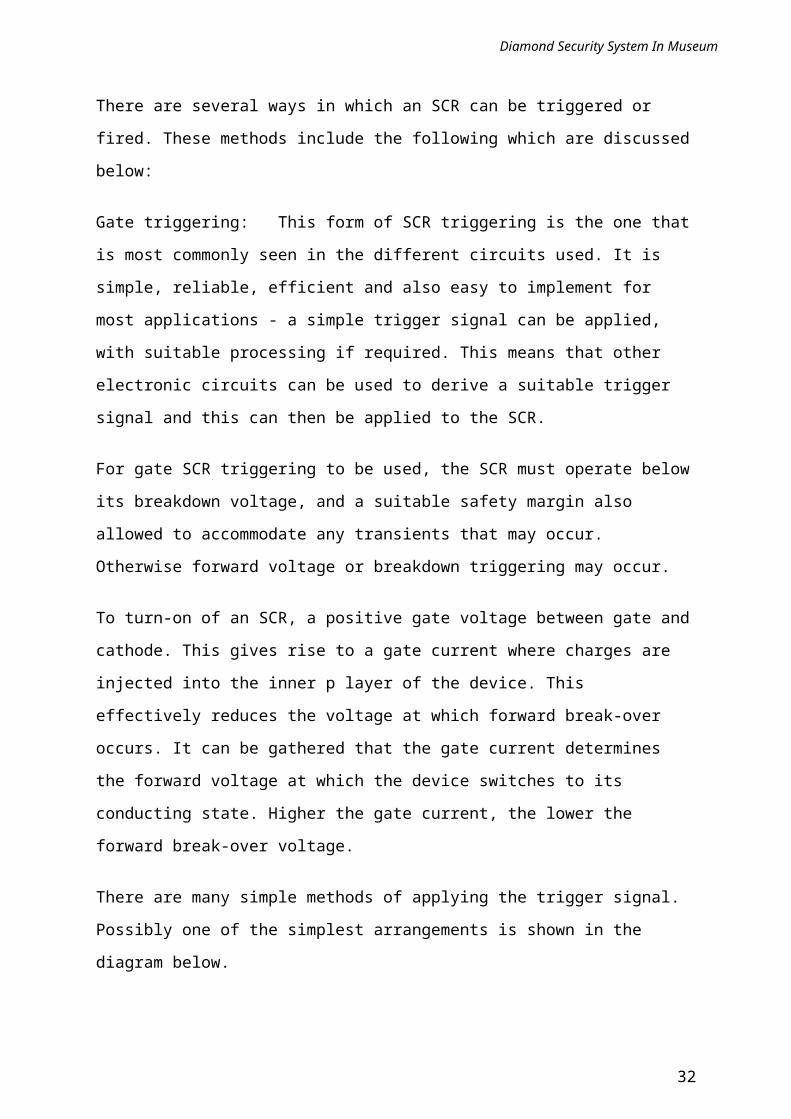
There are several ways in which an SCR can be triggered or fired. These methods include the
following which are discussed below:
Gate triggering: This form of SCR triggering is the one that is most commonly seen in the
different circuits used. It is simple, reliable, efficient and also easy to implement for most
applications - a simple trigger signal can be applied, with suitable processing if required. This
means that other electronic circuits can be used to derive a suitable trigger signal and this can
then be applied to the SCR.
For gate SCR triggering to be used, the SCR must operate below its breakdown voltage, and a
suitable safety margin also allowed to accommodate any transients that may occur. Otherwise
forward voltage or breakdown triggering may occur.
To turn-on of an SCR, a positive gate voltage between gate and cathode. This gives rise to a
gate current where charges are injected into the inner p layer of the device. This effectively
reduces the voltage at which forward break-over occurs. It can be gathered that the gate
current determines the forward voltage at which the device switches to its conducting state.
Higher the gate current, the lower the forward break-over voltage.
There are many simple methods of applying the trigger signal. Possibly one of the simplest
arrangements is shown in the diagram below.
Gate resistors in SCR circuit
24
Diamond Security System In Museum
Here is can be seen that there are two resistors. The first is R1 which is included to limit the
gate current to an acceptable level. This resistor is chosen to provide sufficient current to
trigger the SCR while maintaining it within safe limits for the device. It can easily be
calculated using the device ratings and Ohms law.
The second resistor, R2 is the gate cathode resistor. This is sometimes denoted as RGK and it
is included to prevent spurious triggering. The action of the resistor can be seen with respect
to the two transistor analogy of the SCR. It shows that a low external resistance between the
gate and cathode bypasses some current around the gate junction. Accordingly a higher anode
current is required to initiate and maintain conduction. It is particularly found that low current
high sensitivity SCRs are triggered at very low current levels and therefore an external gate-
cathode resistance is required to prevent triggering by thermally generated leakage current in
the gate region. However the gate cathode resistance bypasses some of the internal anode
current caused by the rapid rate of change of the anode voltage (dv/dt). It also raises the
forward break-over voltage by reducing the efficiency of the NPN transistor region thus
requiring a somewhat higher avalanche multiplication effect to initiate the triggering. The
current that bypasses the gate junction also affects the latching and holding currents.
It can therefore be seen that the effects of using the gate cathode bypass resistor include:
Increase the dv/dt capability.
Retain gate damping to assure the maximum repetitive peak off-state voltage VDRM
capability.
25

Diamond Security System In Museum
Lower the turn-off time, tq.
Raise latching and holding current levels
Although the simple circuit shown above is adequate for many applications, where a more
controlled triggering mechanism is required, account needs to be taken of the gate
characteristics before triggering, during triggering and afterwards. This is required because
the gate characteristics change as a result of the current changes within the device.
Anode cathode forward voltage SCR triggering: This form of SCR triggering or firing
occurs when the voltage between the anode and cathode causes avalanche conduction to take
place. The way in which this occurs can be seen in conjunction with the SCR structure.
SCR Structure
When the anode to cathode forward voltage is increased, diode junction, J2, comes under
increasing stress as it is reverse biased. Ultimately the voltage gradient will increase beyond
the breakdown point and avalanche breakdown will occur triggering the SCR. The voltage at
which this occurs is known as the forward break-over voltage VB0.
As the junction J2 breaks down, current will flow and triggering the SCR to its conducting
state. The junctions J1, J3 are already forward biased, and therefore the breakdown of
junction J2 allows the flow of carriers across all three junctions enabling the load current to
flow. As with other forms of triggering the SCR, the device remains in its conducting
condition.
26
Diamond Security System In Museum
The use of this method of turning the device on is not advised because exceeding the value of
VB0 could destroy the device. Any circuit should be designed to avoid this method of
triggering, noting the maximum of any likely voltage spikes.
Temperature triggering: This form of SCR triggering may occur under some
circumstances. It may give rise to unexpected responses and therefore its effects should be
noted as part of any design process.
Temperature triggering of SCRs occurs as the voltage across the junction J2 and any leakage
current may raise the temperature of the junction. The increase in temperature further
increases the temperature which will in turn increase the leakage current. This cumulative
process may be sufficient to trigger the SCR, although it tends to only occur when the device
temperature is high.
Light triggering: This form of SCR triggering or firing is often used with high voltage
systems. Here an electrical connection is not required from the firing mechanism, and an
isolated light source can be used.
Where light SCR triggering is to be used, specially manufactured SCRs are available. The
light triggering occurs within the inner P-type later. When this area is irradiated by light, free
charge carriers are generated and just like applying a gate signal, the SCR is triggered.
To achieve the maximum light absorption, specialised SCR structures are used, often having
a recess in the inner P-type later to enable maximum access to the light.
To enable the light triggering to take place, light is often directed to the correct point in the
SCR using optical fibre. Once the light exceeds a certain intensity, switching occurs. An SCR
of this type is often referred to as a Light-activated SCR or LASCR. These LASCRs have
been used in high voltage power distribution switching centres. The optical switching enables
very high levels of isolation to be achieved while still being able to switch with low level
circuitry.
dv/dt triggering: SCR triggering can also occur without any gate current if the rate of rise
of anode to cathode voltage exceeds certain limits for the particular device.
27
Diamond Security System In Museum
Although there are several forms of SCR triggering or SCR firing, not all are applicable for
use. However it is necessary to be aware of SCR triggering mechanisms such as forward
breakdown in order to know they exist and should be avoided..
Transistor Relay Driver
The basic transistor relay driver circuit is shown in fig. We’ve added ammeters to measure
the base and collector currents as well as voltmeters to measure the voltage across the
transistor and the relay coil.
28
Diamond Security System In Museum
SOFTWARE USED
MPLAB
MPLAB Integrated Development Environment (IDE) is a free, integrated toolset for the
development of embedded applications employing Microchip's PIC® and dsPIC®
microcontrollers.
MPLAB IDE runs as a 32-bit application on MS Windows®, is easy to use and includes a
host of free software components for fast application development and super-charged
debugging.
MPLAB IDE also serves as a single, unified graphical user interface for additional Microchip
and third party software and hardware development tools. Moving between tools is a snap,
and upgrading from the free software simulator to hardware debug and programming tools is
done in a flash because MPLAB IDE has the same user interface for all tools.
MPLAB SIM, high speed software simulator for PIC and dsPIC devices with peripheral
simulation, complex stimulus injection and register logging.
29
Diamond Security System In Museum
HARDWARE COMPONENTS
STEPPER MOTORS:
A stepper motor is an electro-mechanical device which converts electrical pulses into
discrete mechanical movements. The shaft or spindle of a stepper motor rotates in discrete
step increments when electrical command pulses are applied to it in the proper sequence. The
motors rotation has several direct relationships to these applied input pulses. The sequence of
the applied pulses is directly related to the direction of motor shafts rotation. The speed of the
motor shafts rotation is directly related to the frequency of the input pulses and the length of
rotation is directly related to the number of input pulses applied.
5.1 STEPPER MOTOR ADVANTAGES AND DISADVANTAGES:
ADVANTAGES:
1. The rotation angle of the motor is proportional to the input pulse.
2. The motor has full torque at standstill (if the windings are energized)
3. Precise positioning and repeatability of movement since good stepper motors have an
accuracy of 3 – 5% of a step and this error is non cumulative from one step to the
next.
4. Excellent response to starting/stopping/reversing.
5. Very reliable since there are no contact brushes in the motor. Therefore the life of the
motor is simply dependant on the life of the bearing.
6. The motors response to digital input pulses provides open-loop control, making the
motor simpler and less costly to control.
7. It is possible to achieve very low speed synchronous rotation with a load that is
directly coupled to the shaft.
8. A wide range of rotational speeds can be realized as the speed is proportional to the
frequency of the input pulses.
DISADVANTAGES:
1. Resonances can occur if not properly controlled.
2. Not easy to operate at extremely high speeds.
30

Diamond Security System In Museum
5.2 DC MOTORS VS. STEPPER MOTORS:
1. Stepper motors are operated open loop, while most DC motors are operated closed
loop.
2. Stepper motors are easily controlled with microprocessors; however logic and drive
electronics are more complex.
3. Stepper motors are brushless and brushes contribute several problems, e.g., wear,
sparks, electrical transients.
4. DC motors have a continuous displacement and can be accurately positioned, whereas
stepper motor motion is incremental and its resolution is limited to the step size.
5. Stepper motors can slip if overloaded and the error can go undetected. (A few stepper
motors use closed-loop control.)
6. Feedback control with DC motors gives a much faster response time compared to
stepper motors.
5.3 STEPPER MOTOR BASICS:
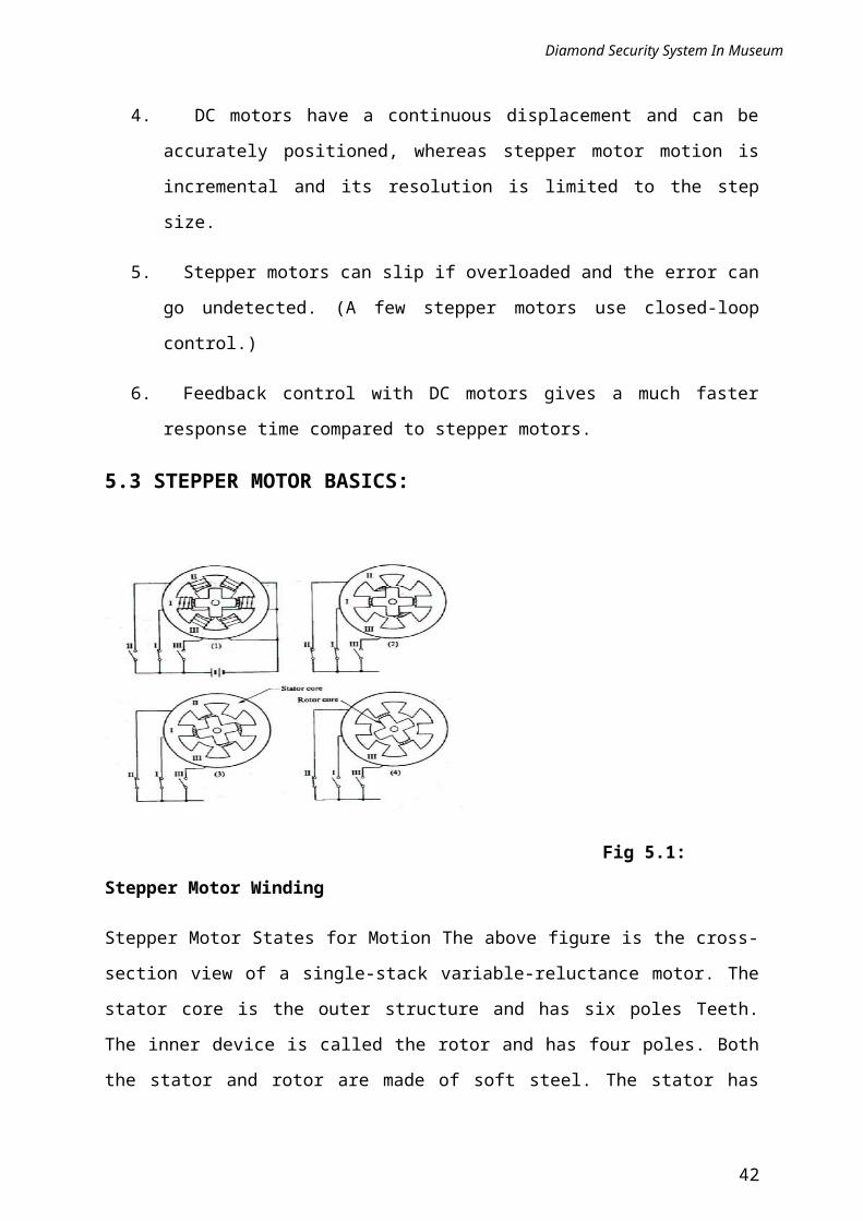
Fig 5.1: Stepper Motor Winding
Stepper Motor States for Motion The above figure is the cross-section view of a single-stack
variable-reluctance motor. The stator core is the outer structure and has six poles Teeth. The
inner device is called the rotor and has four poles. Both the stator and rotor are made of soft
steel. The stator has three sets of windings as shown in the figure. Each set has two coils
31
Diamond Security System In Museum
connected in series. A set of windings is called a “phase”. The motor above, using this
designation, is a three-phase motor. Current is supplied from the DC power source to the
windings via the switches I, II, and, III.
Starting with state (1) in the upper left diagram, note that in state (1), the winding of
Phase I is supplied with current through switch I. This is called in technical terms, “phase I is
excited”. Arrows on the coil windings indicate the magnetic flux, which occurs in the air-gap
due to the excitation. In state I, the two starting poles on phase I being excited are in
alignment with two of the four rotor teeth. This is an equilibrium state. Next, switch II is
closed to excite phase II in addition to phase I. Magnetic flux is built up at the stator poles of
phase II in the manner shown in state (2), the upper right diagram. A counter-clockwise
torque is created due to the “tension” in the inclined magnetic flux lines. The rotor will begin
to move and achieve state (3), the lower left diagram. In state (3) the rotor has moved 15°.
When switch I is opened to de-energize phase I, the rotor will travel another 15° and reach
state (4). The angular position of the rotor can thus be controlled in units of the step angle by
a switching process. If the switching is carried out in sequence, the rotor will rotate with a
stepped motion; the switching process can also control the average speed.
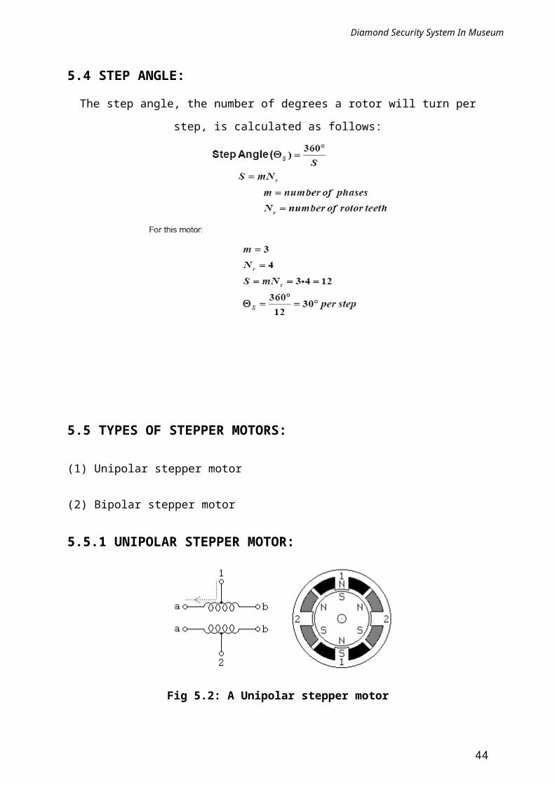
5.4 STEP ANGLE:
The step angle, the number of degrees a rotor will turn per step, is calculated as follows:
32

Diamond Security System In Museum
5.5 TYPES OF STEPPER MOTORS:
(1) Unipolar stepper motor
(2) Bipolar stepper motor
5.5.1 UNIPOLAR STEPPER MOTOR:
Fig 5.2: A Unipolar stepper motor
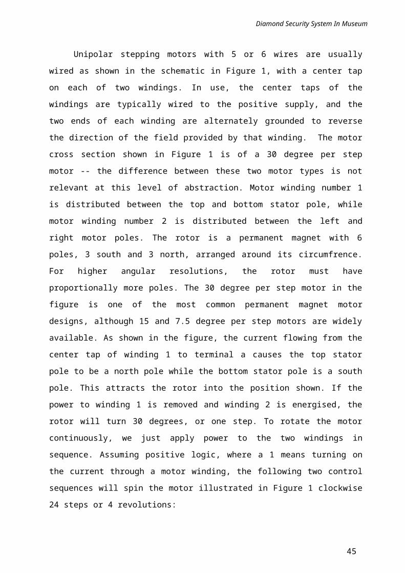
Unipolar stepping motors with 5 or 6 wires are usually wired as shown in the schematic
in Figure 1, with a center tap on each of two windings. In use, the center taps of the windings
are typically wired to the positive supply, and the two ends of each winding are alternately
grounded to reverse the direction of the field provided by that winding. The motor cross
section shown in Figure 1 is of a 30 degree per step motor -- the difference between these two
motor types is not relevant at this level of abstraction. Motor winding number 1 is distributed
between the top and bottom stator pole, while motor winding number 2 is distributed between
the left and right motor poles. The rotor is a permanent magnet with 6 poles, 3 south and 3
north, arranged around its circumfrence. For higher angular resolutions, the rotor must have
proportionally more poles. The 30 degree per step motor in the figure is one of the most
common permanent magnet motor designs, although 15 and 7.5 degree per step motors are
widely available. As shown in the figure, the current flowing from the center tap of winding 1
to terminal a causes the top stator pole to be a north pole while the bottom stator pole is a south
pole. This attracts the rotor into the position shown. If the power to winding 1 is removed and
winding 2 is energised, the rotor will turn 30 degrees, or one step. To rotate the motor
continuously, we just apply power to the two windings in sequence. Assuming positive logic,
where a 1 means turning on the current through a motor winding, the following two control
sequences will spin the motor illustrated in Figure 1 clockwise 24 steps or 4 revolutions:
33

Diamond Security System In Museum
Winding 1a 1000100010001000100010001Winding 1b 0010001000100010001000100Winding 2a 0100010001000100010001000Winding 2b 0001000100010001000100010 time ---> Winding 1a 1100110011001100110011001Winding 1b 0011001100110011001100110Winding 2a 0110011001100110011001100Winding 2b 1001100110011001100110011 time --->
Note that the two halves of each winding are never energized at the same time. Both
sequences shown above will rotate a permanent magnet one step at a time. The top sequence
only powers one winding at a time, as illustrated in the figure above; thus, it uses less power.
The bottom sequence involves powering two windings at a time and generally produces a
torque about 1.4 times greater than the top sequence while using twice as much power.
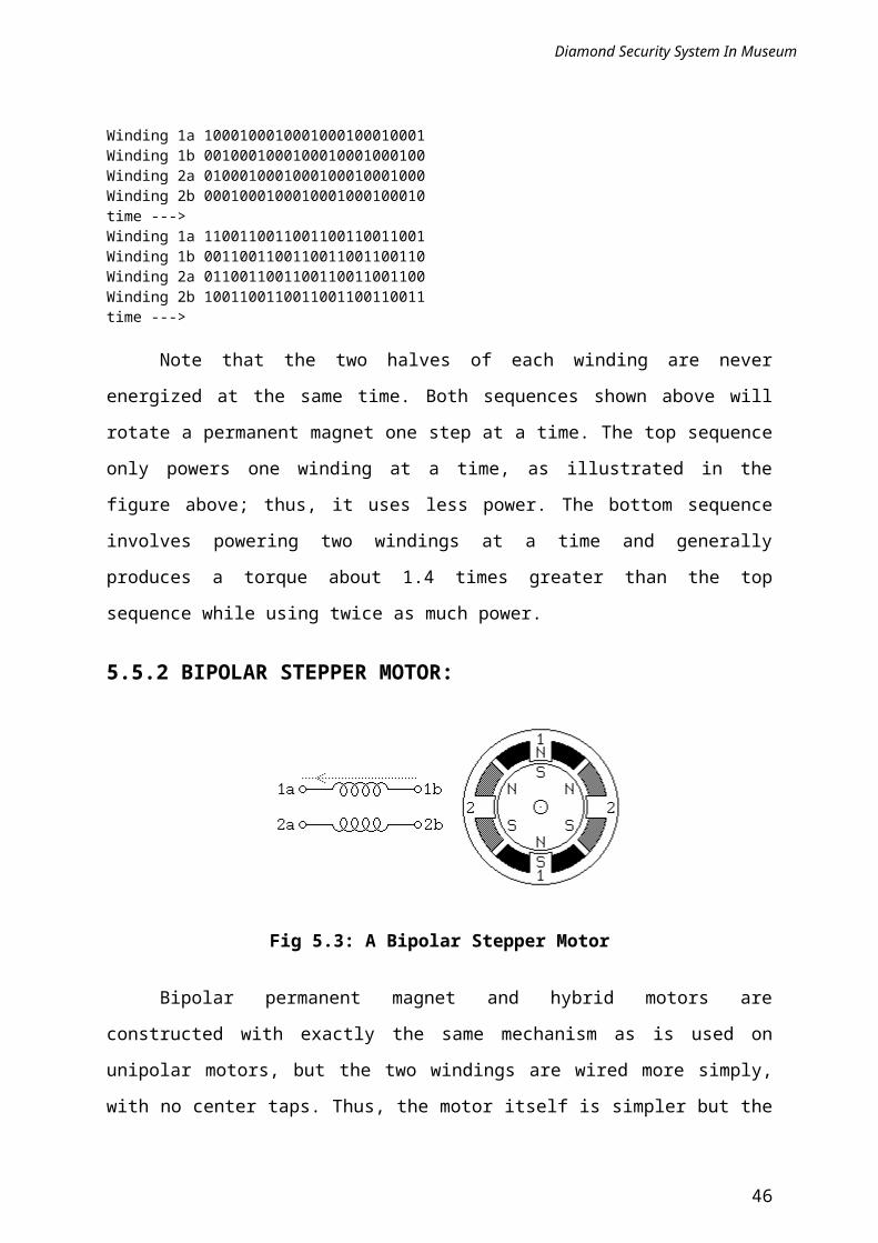
5.5.2 BIPOLAR STEPPER MOTOR:
Fig 5.3: A Bipolar Stepper Motor
Bipolar permanent magnet and hybrid motors are constructed with exactly the same
mechanism as is used on unipolar motors, but the two windings are wired more simply, with
no center taps. Thus, the motor itself is simpler but the drive circuitry needed to reverse the
polarity of each pair of motor poles is more complex. The schematic in Figure 2 shows how
such a motor is wired, while the motor cross section shown here is exactly the same as the
cross section shown in Figure 1. The drive circuitry for such a motor requires an H-bridge
control circuit for each winding. Briefly, an H-bridge allows the polarity of the power applied
to each end of each winding to be controlled independently. The control sequences for single
stepping such a motor are shown below, using + and - symbols to indicate the polarity of the
power applied to each motor terminal:
34

Diamond Security System In Museum
Terminal 1a +---+---+---+---
Terminal 1b --+---+---+---+-
Terminal 2a -+---+---+---+--
Terminal 2b ---+---+---+---+
time --->
Note that these sequences are identical to those for a unipolar permanent magnet
motor, at an abstract level, and that avove the level of the H-bridge power switching
electronics, the control systems for the two types of motor can be identical. Note that many
full H-bridge driver chips have one control input to enable the output and another to control
the direction. Given such bridge chips, one for eachwinding, the following control sequences
will spin the motor identically to the control sequences given above:
Enable 1 1111111111111111
Direction 1 1100110011001100
Enable 2 1111111111111111
Direction 2 0110011001100110
time --->
To distinguish a bipolar permanent magnet motor from other 4 wire motors, measure
the resistances between the different terminals. It is worth noting that some permanent
magnet stepping motors have 4 independent windings, organized as two sets of two. Within
each set, if the two windings are wired in series, the result can be used as a high voltage
bipolar motor. If they are wired in parallel, the result can be used as a low voltage bipolar
motor. If they are wired in series with a center tap, the result can be used as a low voltage
unipolar motor.
5.6 MOTOR CONTROL CIRCUITRY:
35

Diamond Security System In Museum
Fig 5.4: Magnetic Field Diagram
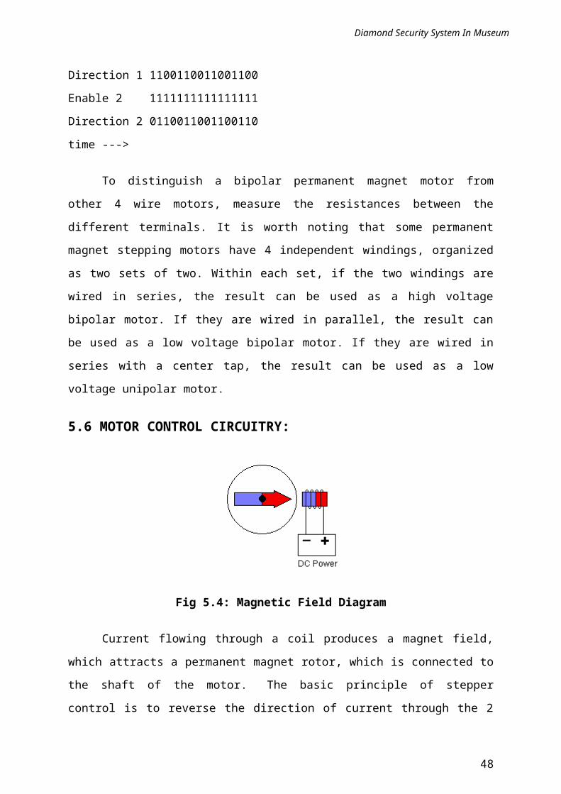
Current flowing through a coil produces a magnet field, which attracts a permanent
magnet rotor, which is connected to the shaft of the motor. The basic principle of stepper
control is to reverse the direction of current through the 2 coils of a stepper motor, in
sequence, in order to influence the rotor. Since there are 2 coils and 2 directions, that gives
us a possible 4-phase sequence. All we need to do is get the sequencing right and the motor
will turn continuously. You may wonder how the stepper can achieve such fine stepping
increments with only a 4-phase sequence. The internal arrangement of the motor is quite
complex- the winding and core repeating around the perimeter of the motor many times. The
rotor is advanced only a small angle, either forward or reverses, and the 4-phase sequence is
repeated many times before a complete revolution occurs.
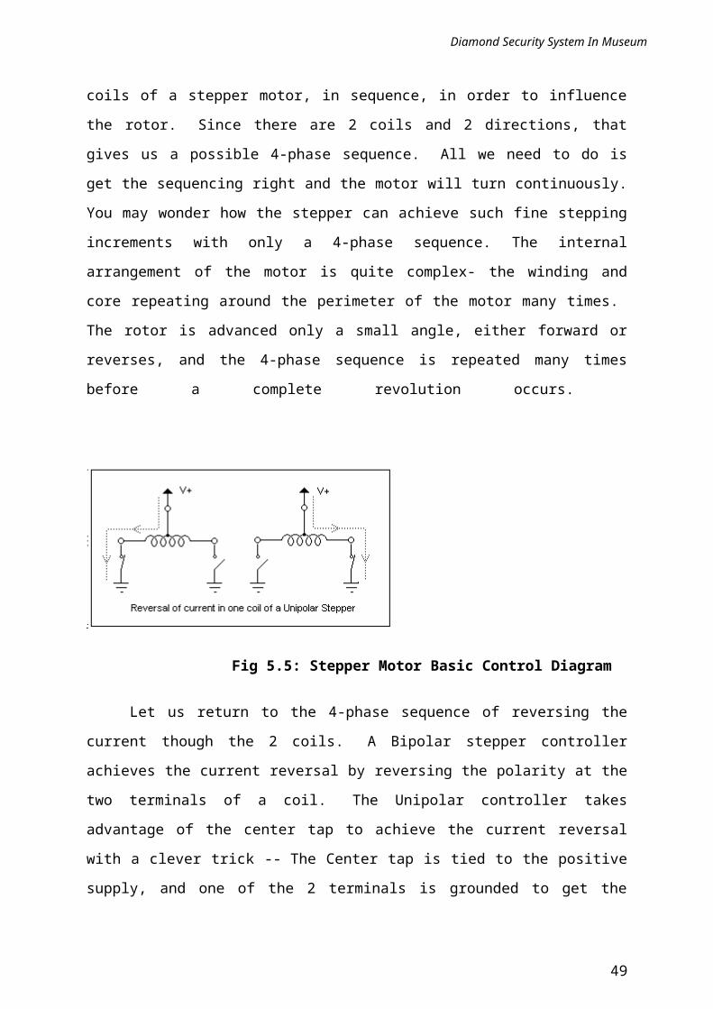
Fig 5.5: Stepper Motor Basic Control Diagram
Let us return to the 4-phase sequence of reversing the current though the 2 coils. A
Bipolar stepper controller achieves the current reversal by reversing the polarity at the two
terminals of a coil. The Unipolar controller takes advantage of the center tap to achieve the
current reversal with a clever trick -- The Center tap is tied to the positive supply, and one of
the 2 terminals is grounded to get the current flowing one direction. The other terminal is
grounded to reverse the current. Current can thus flow in both directions, but only half coils
are energized at a time. Both terminals are never grounded at the same time, which would
energize both coils.
5.7 CONCEPTUAL STUDY OF UNISTEPPER MOTOR:
36

Diamond Security System In Museum
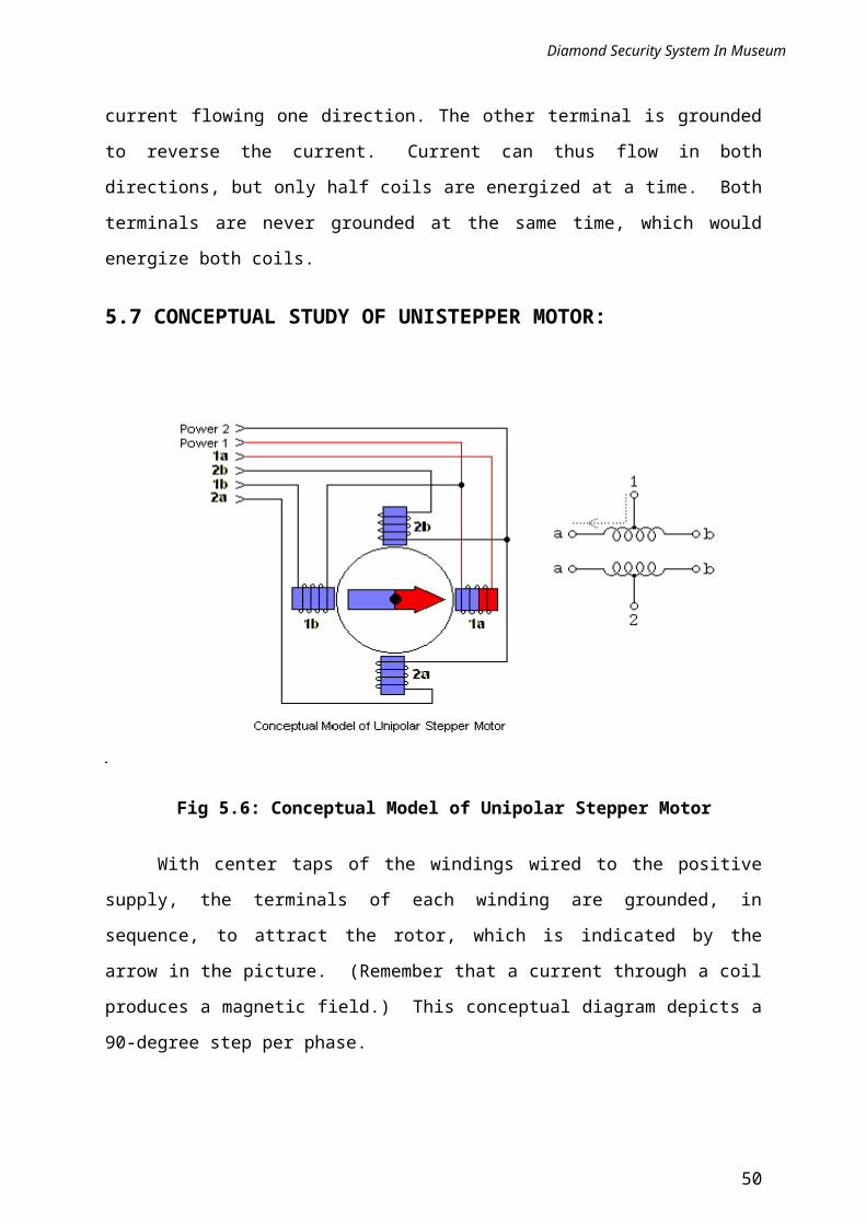
Fig 5.6: Conceptual Model of Unipolar Stepper Motor
With center taps of the windings wired to the positive supply, the terminals of each
winding are grounded, in sequence, to attract the rotor, which is indicated by the arrow in the
picture. (Remember that a current through a coil produces a magnetic field.) This conceptual
diagram depicts a 90-degree step per phase.
In a basic "Wave Drive" clockwise sequence, winding 1a is de-activated and winding
2a activated to advance to the next phase. The rotor is guided in this manner from one
winding to the next, producing a continuous cycle. Note that if two adjacent windings are
activated, the rotor is attracted mid-way between the two windings. The following table
describes 3 useful stepping sequences and their relative merits. The sequence pattern is
represented with 4 bits, a '1' indicates an energized winding. After the last step in each
sequence the sequence repeats. Stepping backwards through the sequence reverses the
direction.
5.8 WAVE STEPPING:
The wave stepping sequence is shown below.
STEP L1 L2 L3 L4
37

Diamond Security System In Museum
1 H L L L
2 L H L L
3 L L H L
4 L L L H
Wave stepping has less torque then full stepping. It is the least stable at higher speeds and as low power consumption.
5.8.1 FULL STEPPING:
The full stepping sequence is shown below.
STEP L1 L2 L3 L4
1 H H L L
2 L H H L
3 L L H H
4 H L L H
Full stepping has the lowest resolution and is the strongest at holding its position. Clock-wise and counter clockwise rotation is accomplished by reversing the step sequence.
5.8.2 HALF STEPPING:
A Combination of Wave and Full Stepping
The half-step sequence is shown below.
STEP L1 L2 L3 L4
1 H L L L
2 H H L L
3 L H L L
4 L H H L
5 L L H L
38

Diamond Security System In Museum
6 L L H H
7 L L L H
8 H L L H
The half-step sequence has the most torque and is the most stable at higher speeds. It
also has the highest resolution of the main stepping methods. It is a combination of full and
wave stepping.
5.9 RS 232:
. All IBM PC and compatible computers are typically equipped with two serial ports
and one parallel port. Although these two types of ports are used for communicating with
external devices, they work in different ways
A parallel port sends and receives data eight bits at a time over 8 separate wires. This
allows data to be transferred very quickly; however, the cable required is more bulky because
of the number of individual wires it must contain. Parallel ports are typically used to connect
a PC to a printer and are rarely used for much else.
A serial port sends and receives data one bit at a time over one wire. While it takes
eight times as long to transfer each byte of data this way, only a few wires are required. In
fact, two-way (full duplex) communications is possible with only three separate wires - one
to send, one to receive, and a common signal ground wire. The serial port on our PC is a full-
duplex device meaning that it can send and receive data at the same time. In order to be able
to do this, it uses separate lines for transmitting and receiving data. Some types of serial
devices support only one-way communications and therefore use only two wires in the cable -
the transmit line and the signal ground.
RS-232 stands for Recommend Standard number 232 and C is the latest revision of
the standard. The serial ports on most computers use a subset of the RS-232C standard. The
full RS-232C standard specifies a 25-pin "D" connector of which 22 pins are used. Most of
these pins are not needed for normal PC communications, and indeed, most new PCs are
equipped with male D type connectors having only 9 pins.
5.10 PC INTERFACE SECTION:
39
1
2
3
4

Diamond Security System In Museum
Fig 5.7: RS-232 Connecter diagram
The above shown connector known as 9-pin, D-type male connector is used for
RS232 connections. The pin description is given in the following table.
Table 5.1: RS-232 pin details
We cannot simply connect our system to this terminal without providing proper hand
shaking signal. For communicating with RS-232 type equipment, the /RTS of the connector
is simply looped into the /CTS, so /CTS will automatically be asserted when /RTS is asserted
internally. Similarly the /DTR is looped into /DSR and /CD, so when PC asserts its /DTR
output the /DSR and /CD inputs are automatically be asserted. These connections do not
provide for any hardware hand shaking. They are necessary to get the PC and our system talk
each other. The connection diagram is shown below. We cannot simply connect our system to
this terminal without providing proper hand shaking signal. For communicating with RS-232
type equipment, the /RTS of the connector is simply looped into the /CTS, so /CTS will
40
Pin No. Common
Name
RS232
name
Description Signal
direction
1 /CD CF Received line signal detector IN
2 RXD BB Received data IN
3 TXD BA Transmitted data OUT
4 /DTR CD Data terminal ready OUT
5 GND AB Signal ground --
6 /DSR CC Data set ready IN
7 /RTS CA Request to send OUT
8 /CTS CB Clear to send IN

Diamond Security System In Museum
automatically be asserted when /RTS is asserted internally. Similarly the /DTR is looped
into /DSR and /CD, so when PC asserts its /DTR output the /DSR and /CD inputs are
automatically be asserted. These connections do not provide for any hardware hand shaking.
They are necessary to get the PC and our system talk each other. The connection diagram is
shown below.
Fig 5.8: RS-232 Interface diagram
5.11 RS-232 SERIAL INTERFACE:
The MAX232 I.C convert input TTL level into RS-232C standard level and
connected to PC through 9-pin D-type connector. Now discuss about standards of RS232 and
Serial communication through RS232
41
Tx 3 Rx 2
/CTS 8
/RTS 7
/DSR 6
/DTR 4
2 Rx
3 Tx
Diamond Security System In Museum
Fig 5.9: RS 232 Circuit diagram
RS-232 logic levels are indicated by positive and negative voltages, rather than by the
positive-only signals of 5V TTL and CMOS logic. At an RS-232 data output (TD), a logic 0
is defined as equal to or more positive than +5V, and a logic 1 is defined as equal to or more
negative than –5V. In other words, the signals use negative logic, where the more negative
voltage is logic 1.
The control signals use the same voltages, but with positive logic. A positive voltage
indicates that the function is on, or asserted, and a negative voltage indicates that the function
is off, or not asserted.
RS-232 interface chips invert the signals. On a UART’s output pin, a logic-1 data bit
or an off control signal is near 5V, which results in a negative voltage at the RS-232
interface. Logic – 0 data bit or on control signal is near 0V, resulting in a positive voltage at
the RS-232 interface. Because an RS-232 receiver may be at the end of a long cable, by the
time the signal reaches the receiver, its voltage may have attenuated or have noise riding on
it. To allow for this, the minimum required voltages at the receiver are less than at the driver.
An input more positive than +3V is a logic 0 at RD, or On at a control input. An input more
negative than –3V is a logic 1 at RD, or Off at a control input. According to the standard, the
logic level of an input between –3V and +3V is undefined.
The noise margin, or voltage margin, is the difference between the output and input
voltages. RS-232’s large voltage swings result in a much wider noise margin than 5V TTL
logic. For example, even if an RS-232 driver’s output is the minimum +5V, it can attenuate
or have noise spikes as large as 2V at the receiver and still be a valid logic 0. Many RS-232
outputs have much wider voltage swings: 9 and 12V are common. These in turn give
much wider noise margin. The maximum allowed voltage swing is 15V, though receivers
must handle voltages as high as 25V without damage.
Two other terms used in relation to RS-232 are Mark and Space. Space is logic 0, and
Mark is logic 2. These refer to the physical marks and spaces made by the mechanical
recorders used years ago to log binary data.
42

Diamond Security System In Museum
TIA/EIA-232 includes both minimum and maximum timing specifications. All of the
many RS-232 interface chips meet these specifications. The specified slew rate limits the
maximum bit rate of the interface. Slew rate is a measure of how fast the voltage changes
when the output switches and describes an output’s instantaneous rate of voltage change. The
slew rate of an RS-232 driver must be 30 Volts per microsecond or less. The advantage of
limiting slew rate is that it improves signal quality by virtually eliminating problems due to
voltage reflections that occur on long links that carry signals. With fast rise and fall times.
But the slew rate also limits a link’s maximum speed. At 30 V/s, an output requires 0.3
microsecond to switch from +5V to –5V. RS-232’s specified maximum bit rate is 20 kbps,
which translates to a bit width of 50 microseconds, or 166 times the switching time at the
fastest allowed slew rate.
5.12 ULN2803
The ULN2801A-ULN2805A each contains eight Darlington transistors with common
emitters and integral suppression diodes for inductive loads. Each Darlington features a peak
load current rating of 600mA (500mA continuous) and can withstand at least50V in the off
state. Outputs maybe paralleled or higher current capability. Five versions are available to
simplify interfacing to standard logic families: the ULN2801Ais designed for general purpose
applications with a current limit resistor; theULN2802A has a 10.5kW input resistor and
zener for 14-25VPMOS; theULN2803Ahas a 2.7kW input resistor for 5V TTL and CMOS;
the ULN2804A has a 10.5kW input resistor for 6-15V CMOS and the ULN2805A is
designed to sink a minimum of 350mA for standard and Schottky TTL where higher output
current is required. All types are supplied in a 18-lead plastic DIP with a copper lead from
and feature the convenient input opposite- output pin out to simplify board layout.
43
Diamond Security System In Museum
Fig 5.10: Pin Assignment of ULN2803
Fig 5.11: Circuit Diagram of ULN 2803
44
Diamond Security System In Museum
5.13 LIGHT EMITTING DIODE:
A light-emitting diode (LED) is a semiconductor device that emits incoherent narrow-
spectrum light when electrically biased in the forward direction of the p-n junction. This
effect is a form of electroluminescence.
An LED is usually a small area source, often with extra optics added to the chip to
shape its radiation pattern [10]. The color of the emitted light depends on the composition and
condition of the semiconducting material used, and can be infrared, visible, or near-
ultraviolet.
Fig 5.12: LED
45
Diamond Security System In Museum
TYPE OF COLOURS:
1. Red
2. Green
3. Yellow
ADVANTAGES:
1. Low working voltages and currents
2. Less consumption
3. Very fast action
4. Small size and weight
5. Extremely long life
5.14 BC 547 TRANSISTOR:
BC547 is an NPN bi-polar junction transistor. A transistor, stands for transfer of
resistance, is commonly used to amplify current. A small current at its base controls a larger
current at collector & emitter terminals. BC547 is mainly used for amplification and
switching purposes. It has a maximum current gain of 800. Its equivalent transistors are
BC548 and BC549.
The transistor terminals require a fixed DC voltage to operate in the desired region of
its characteristic curves. This is known as the biasing. For amplification applications, the
transistor is biased such that it is partly on for all input conditions. The input signal at base is
amplified and taken at the emitter. BC547 is used in common emitter configuration for
amplifiers. The voltage divider is the commonly used biasing mode. For switching
applications, transistor is biased so that it remains fully on if there is a signal at its base. In
the absence of base signal, it gets completely off.
46

Diamond Security System In Museum
Fig 5.13: BC 547 Transistor
47
Diamond Security System In Museum
CHAPTER 6
RESULTS
6.1 RESULT:
By this way we can protect the costliest items like diamond etc in highly secured way by the sensor and no man is required for the security.
6.2 APPLICATIONS:
Home
Offices
Jewellery shops
Banks
Museums
6.3 ADAVANTAGES:
Fit and Forget system
Low cost and Reliable Circuit
Complete elimination of Man Power
Loud Siren Sound up to 60 dB
System can be armed/disarmed by owner only
48
Diamond Security System In Museum
CHAPTER 7
FUTURE SCOPE
7.1 FUTURE SCOPE:
Embedded system is an emerging field and there is a huge scope for research and
development. This would be especially helpful in over come from damages of products or
devices due to increase in temperature without man power.
7.2 CONCLUSION:
The project “DIAMOND SECURITY SYSTEM IN MUSEUM” has been
successfully designed and tested. It has been developed by integrating features of all the
hardware components used. Presence of every module has been reasoned out and placed
carefully thus contributing to the best working of the unit.
Secondly, using highly advanced IC’s and with the help of growing technology the
project has been successfully implemented.
Finally we conclude that embedded system is an emerging field and there is a huge
scope for research and development.
49
Diamond Security System In Museum
PICTORIAL REPRESENTATION OF THE KIT:
50