dielectric prism antenna - em labemlab.utep.edu/pdfs/msthesis_joseavila.pdf · dielectric prism...
TRANSCRIPT

DIELECTRIC PRISM ANTENNA
JOSE ANTONIO AVILA
Master’s or Doctoral Program in Electrical Engineering
APPROVED:
Raymond Rumpf, Ph.D., Chair
Virgilio Gonzalez, Ph.D.
Son-Young Yi, Ph.D.
Charles Ambler, Ph.D.
Dean of the Graduate School

Copyright ©
by
Jose Avila
2016

Dedication
This work is dedicated to my family whose love, support and patience has pushed me to
accomplish so much.

DIELECTRIC PRISM ANTENNA
by
JOSE ANTONIO AVILA
THESIS
Presented to the Faculty of the Graduate School of
The University of Texas at El Paso
in Partial Fulfillment
of the Requirements
for the Degree of
Master of Science
Department of Electrical and Computer Engineering
THE UNIVERSITY OF TEXAS AT EL PASO
May 2016

v
Acknowledgements
Thank you, Dr. Rumpf, Carlos Rodriguez, Cesar Valle, Ubaldo Robles, Eric Berry for their
help and the rest of the members of the EM Lab as well. I would also like to thank Laird
Technologies and NPS. Most of all thank you to my family who made this possible.

vi
Abstract
3D printing is revolutionizing the development and manufacturing of devices. Currently
multi-material 3D printing, like metals plus dielectrics, is in the early stages and not very
accessible. This work set out to develop an all-dielectric antenna that could be 3D printed with
current widely accessible 3D printing technologies. The antenna developed is an all-dielectric
ultra-thin antenna with a simple geometry. The antenna radiates by using total internal reflection
and a circulating mode operating as a leaky whispering gallery mode. We are calling the antenna
the dielectric prism antenna because it acts like an optical prism. The dielectric prism antenna was
developed in stages with increasing complexity. First, a one dimensional simulation of a slab
waveguide analysis was performed to answer if a usable guided mode was present. Then a two
dimensional simulation using finite-difference frequency domain method to visualize steady state
fields. The design of the antenna was finalized in a rigorous 3D simulation with the commercial
software package, ANSYS HFSS. The antenna was then manufactured and tested resulting in a
dielectric prism antenna with a thickness of 1.5 mm operating at 2.4 GHz.

vii
Table of Contents
Acknowledgements ..........................................................................................................................v
Abstract .......................................................................................................................................... vi
Table of Contents .......................................................................................................................... vii
List of Figures .............................................................................................................................. viii
Chapter 1: Introduction ....................................................................................................................1
1.1 Background .......................................................................................................................2
1.1.1 3D Printing ............................................................................................................2
1.1.2 Dielectric Antennas ...............................................................................................2
Chapter 2 – Computational Electromagnetic Methods ....................................................................4
2.1 Maxwell’s Equations ........................................................................................................4
2.2 Finite-Difference Approximation .....................................................................................7
2.3 Yee Grid ............................................................................................................................8
2.4 Slab Waveguide Analysis ...............................................................................................11
2.5 Finite-Difference Frequency Domain Method ................................................................15
Chapter 3: Dielectric Prism Antenna .............................................................................................20
3.1 Design .............................................................................................................................20
3.2 Manufacturing .................................................................................................................27
3.3 Testing.............................................................................................................................30
Chapter 4: Conclusion....................................................................................................................35
4.1 Future Work ....................................................................................................................35
References ......................................................................................................................................36
Vita 39

viii
List of Figures
Figure 2.6: Slab waveguide analysis example [20]. ..................................................................... 12
Figure 2.7: Gaussian beam source ................................................................................................ 17 Figure 2.8: Total-field/scattered-field framework [19]. ................................................................ 17 Figure 2.9: UPML in the solution space to prevent reflections from the boundaries [23]. .......... 18 Figure 3.1:Design flow for the DPA. ............................................................................................ 20 Figure 3.2: Guided modes from the slab waveguide analysis, horizontal polarization (top),
vertical polarization (bottom). ...................................................................................................... 20 Figure 3.3: Setup used for FDFD, (left) the device, (right) the source. ....................................... 21 Figure 3.4:Resulting fields from the first studied device with FDFD. ......................................... 22
Figure 3.5: Changing the geometry to increase the angle of incidence leads to a circular design.
....................................................................................................................................................... 22 Figure 3.6: Steady-state fields of circular device.......................................................................... 23 Figure 3.7: Exploded view of the antenna with the powder implementation. .............................. 23
Figure 3.8: Feed concepts for the DPA. ........................................................................................ 24 Figure 3.9: Vee dipole feed made from splitting a coaxial cable [24]. ......................................... 25
Figure 3.10: HFSS study of the feed placement. .......................................................................... 25 Figure 3.11: HFSS model for DPA simulation. ............................................................................ 26
Figure 3.12: Study of the impact of thickness and diameter on the radiation pattern [24]. .......... 26 Figure 3.13: HFSS study of antenna efficiency. ........................................................................... 27 Figure 3.14: Steps of the manufacturing of the DPA. ................................................................... 28
Figure 3.15: Shell modeled in Solidworks. ................................................................................... 28
Figure 3.16: 3D printer in the process of printing the top lid [24]. ............................................... 29 Figure 3.17: DPA shell being packed with dielectric powder (left), DPA sealed with epoxy
(right) [24]. .................................................................................................................................... 29
Figure 3.18: Snap lid design for DPA implementation [24]. ........................................................ 30 Figure 3.19: Manufactured DPA with dimensions [24]................................................................ 30 Figure 3.20:Block diagram of reflectance test (left), VNA used for testing (right). .................... 31
Figure 3.21:Block diagram for the radiation pattern test. ............................................................. 31 Figure 3.22: Picture of the setup for the radiation pattern testing. ............................................... 32
Figure 3.23: DPA with thickness of 2.8 mm 11S comparison of simulated and measured data
(left), normalized radiation pattern comparison of simulated and measured data (right). ............ 32
Figure 3.24:DPA with thickness of 1.5 mm 11S comparison of simulated and measured data
(left), normalized radiation pattern comparison of simulated and measured data (right). ............ 33 Figure 3.25:Block diagram for the WiFi test. ............................................................................... 33
Figure 3.26: Picture of a close setup of the WiFi test. .................................................................. 34

1
Chapter 1: Introduction
3D printing is changing manufacturing. The manufacturing process has become more
accessible with 3D printers being widely available. This work aimed to design an antenna that
could be 3D printed. The antenna designed is an all-dielectric ultra-thin antenna that operates like
a prism and is being called the dielectric prism antenna (DPA). Because having an ultra-thin
design, 1.5 mm in the design presented, makes it difficult to establish a resonance with traditional
designs, a novel design taking advantage of total internal reflection (TIR) is used in order to
establish a leaky whispering gallery mode. The DPA presented in this work is of simple geometry
and therefore can be easily 3D printed, in this work the printing process of fused deposition
modeling (FDM) was utilized. The antenna was designed to operate at a frequency of 2.4 GHz in
order to perform a test with WiFi. It was designed to be ultra-thin in order to save on materials and
time, also a monolithic all-dielectric design was implemented in order to try to avoid any post-
processing in manufacturing or extra tools. The DPA was designed in stages with increasing
complexity. The computational methods used in this work utilized the finite-difference
approximation to solve Maxwell’s equations. First, a one dimensional analysis was performed
using slab waveguide analysis. This in order to find if a guided mode existed in a thin slab of
dielectric that could be used for TIR. Second, a two dimensional simulation was performed with
the finite-difference frequency domain method and the steady state fields where visualized. This
step was to confirm if the DPA would resonate. The final design step was a three dimensional
rigorous simulation using the commercial package ANSYS HFSS. This work implemented a proof
of concept antenna utilizing low-loss dielectric powder from Laird Technologies. A shell was 3D
printed through FDM with a Makerbot Replicator 2x. The shell was then packed with dielectric
powder and then sealed. Finally, the DPA was tested using a vector network analyzer (VNA),
reflectance and pattern measurements were performed. The final test was a WiFi where a stock
antenna was replaced with the DPA and a print job was submitted wirelessly. Both the
manufacturing and testing took place at the University of Texas at El Paso EM Lab.

2
1.1 BACKGROUND
1.1.1 3D Printing
3D printing is a developing technology that offers many benefits. It is a widely accessible
process that can be performed by anyone. It allows more freedom in complexity of the design
allowing for more geometries and a high level of customization that weren’t possible before. 3D
printing uses inexpensive materials and it allows for rapid prototyping because the manufacturing
does not require outsourcing. Currently hybrid 3D printing, simultaneous printing of metals plus
dielectric, is in the early stages and is not widely accessible so the cost is very high. Research with
3D printing antennas is being performed at this time using different methods. In [1] an antenna
was 3D printed out of Acrylonitrile Butadiene Styrene (ABS) and after a silver painting
metallization layer was applied in order to make a radiating element. In [2] an antenna printed with
polylactic acid (PLA) and coated with a carbon based conductive black paint is presented. [3]
presents a conical spiral antenna 3D printed of PLA and silver nanoparticle ink. [4] presents a
bowtie antenna 3D printed with PLA and conductive ABS. In [5] micro-dispensing of conformal
antennas is being explored. For the purposes of this work the aim is to keep the 3D printing process
as accessible and simple as possible so a simple FDM printer, Makerbot Replicator 2x, is utilized.
1.1.2 Dielectric Antennas
Dielectric antennas are desirable because they have very low loss and thus are efficient
radiators. The dielectric material is also inexpensive and widely available. There are various forms
of dielectric antennas, in [6] an all-dielectric horn antenna of electromagnetic bandgap structure
with evanescent feeding is presented. In [7] a dielectric rod antenna is designed for ultra-wideband
operation and [8] presents a leaky-wave dielectric antenna. In [9] the most compact of the dielectric
antennas is presented with the dielectric resonator antenna (DRA), so this type was investigated
further.
The DRA started out from components in microwave circuit applications being used as a
high Q factor, quality factor, elements for energy storage. In [9] it was discovered that the DRA

3
is an efficient radiator if the shielding is removed and the proper mode is excited. The resonance
with the DRA is established by the energy clashing up against the walls of the dielectric hitting it
straight on and forming standing waves. There has been a large amount of research on DRAs [10,
11]. The size can be reduced by introducing metal to the design [12] and by increasing the dielectric
constant of the antenna [13]. To date the thinnest dielectric antenna found in literature is [14], this
antenna uses a very high dielectric constant of 1000 and has a thickness of 2.5 mm. The aim of
this project is to have an all-dielectric ultra-thin antenna without using a really high dielectric
constant so it was determined that for such a thin device the resonant mechanism of the DRA
would not work. So a novel concept for an antenna is presented in this work utilizing total internal
reflection (TIR) to excite a leaky whispering gallery mode.

4
Chapter 2 – Computational Electromagnetic Methods
This chapter presents the computational methods used to analyze the antenna. Finite-
difference approximations where used to solve Maxwell’s equations with the constitutive relations.
Two methods where implemented for this project. The first was a one dimensional slab waveguide
analysis which performs an analysis to find what modes exist in a slab. The second method was a
two dimensional finite-difference frequency domain (FDFD) method, which solves and visualizes
steady state fields. Both of these methods where implemented using MATLAB. The commercial
software package ANSYS HFSS was used to perform a rigorous 3D simulation to corroborate the
other simulations and finalize the design of the DPA.
2.1 MAXWELL’S EQUATIONS
We will begin by preparing Maxwell’s equations for the methods [15]. Maxwell’s
equations in differential form in the time domain are
( ) ( )vD t t (2.1)
( ) 0B t (2.2)
( )
( ) ( )D t
H t J tt
(2.3)
( )
( )B t
E tt
(2.4)
Here D is the electric flux density 2/C m , v is the electric charge density 3/C m ,
B is the magnetic flux density 2/W m , H is the magnetic field intensity /A m , J is the
electric current density 2/A m , and E is the electric field intensity /V m .
The constitutive relations describe how waves interact with materials and they are the
following
( ) ( ) ( )D t t E t (2.5)
( ) ( ) ( )B t t H t (2.6)

5
Here is the permittivity /F m , and is the permeability /H m , these are tensors
and the equations in the time domain involve convolutions.
We can convert Maxwell’s equations and the constitutive relations to the frequency domain
and simplify them by assuming no static charges or currents, ( ) 0v J t . We will further
simplify the equations by assuming linear, homogeneous and isotropic materials. This will reduce
the permittivity and permeability tensors to scalars because the material properties are uniform in
all directions. These assumptions will yield the following frequency domain equations
0D (2.7)
0B (2.8)
E j B (2.9)
H j D (2.10)
D E (2.11)
B H (2.12)
We can expand (2.11) and (2.12) by the following relationships
o r (2.13)
o r (2.14)
Here o is the permittivity of free space, r is the relative permittivity or dielectric
constant, o is the permeability of free space and r is the relative permeability. This yields the
following for the constitutive relations
o rD E (2.15)
o rB H (2.16)
We can substitute equations (2.15) and (2.16) into (2.9) and (2.10) to get the following
o rE j H (2.17)

6
o rH j E (2.18)
We can further simplify these equations by normalizing the magnetic field by the following
equation
o
o
H j H
(2.19)
This normalization also provides the benefit that the electric field and magnetic fields will
be of the same magnitude during our computations and thus reduce the loss of significant digits
due to truncation. The resulting equations are
o rE k H (2.20)
o rH k E (2.21)
Where ok is the wave number and is equal to the following
o o ok (2.22)
We can expand equations (2.20) and (2.21) to the following
yz
o r x
EEk H
y z
(2.23)
x zo r y
E Ek H
z x
(2.24)
y x
o r z
E Ek H
x y
(2.25)
yz
o r x
HHk E
y z
(2.26)
x zo r y
H Hk E
z x
(2.27)
y x
o r z
H Hk E
x y
(2.28)
We can further simplify (2.23)-(2.28) by normalizing the spatial coordinates according to
the following

7
' ox k x (2.29)
' oy k y (2.30)
' oz k z (2.31)
Substituting equations (2.29)-(2.31) into equations (2.23)-(2.28) will give the following
' '
yzr x
EEH
y z
(2.32)
' '
x zr y
E EH
z x
(2.33)
' '
y xr z
E EH
x y
(2.34)
' '
yzr x
HHE
y z
(2.35)
' '
x zr y
H HE
z x
(2.36)
' '
y xr z
H HE
x y
(2.37)
These equations will be the starting point for FDFD and slab waveguide analysis.
2.2 FINITE-DIFFERENCE APPROXIMATION
Equations (2.32)-(2.37) contain first order partial derivatives. In order to compute these
partial derivatives a finite-difference approximation will be used. Specifically we will be using a
central finite-difference approximation [16]. The central finite-difference approximation
approximates the derivative at a location by using the next and the previous points.
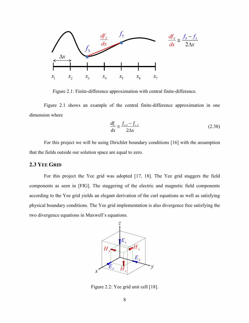
8
Figure 2.1: Finite-difference approximation with central finite-difference.
Figure 2.1 shows an example of the central finite-difference approximation in one
dimension where
1 1
2
i i idf f f
dx x
(2.38)
For this project we will be using Dirichlet boundary conditions [16] with the assumption
that the fields outside our solution space are equal to zero.
2.3 YEE GRID
For this project the Yee grid was adopted [17, 18]. The Yee grid staggers the field
components as seen in [FIG]. The staggering of the electric and magnetic field components
according to the Yee grid yields an elegant derivation of the curl equations as well as satisfying
physical boundary conditions. The Yee grid implementation is also divergence free satisfying the
two divergence equations in Maxwell’s equations.
Figure 2.2: Yee grid unit cell [18].

9
The Yee grid does have the consequence that because the field components are staggered
then the components from the same Yee cell can see different material properties.
Figure 2.3: 2D grid showing the staggering of field components according to the Yee grid [19].
Figure 2.3 shows how the field components are staggered in a two dimensional solution
space according to the Yee grid. The component within the same Yee cell, represented by a 22
cell, can see different material properties. Therefore the permittivity and permeability seen by
components of the same cell can be different and thus will be represented by
, , , , ,xx yy zz xx yy zz . These quantities are not to be confused with anisotropic tensor quantities
but simply represent the material properties seen by the corresponding field component.
Substituting them into (2.32)-(2.37) gives
' '
yzxx x
EEH
y z
(2.39)
' '
x zyy y
E EH
z x
(2.40)
' '
y xzz z
E EH
x y
(2.41)
' '
yzxx x
HHE
y z
(2.42)

10
' '
x zyy y
H HE
z x
(2.43)
' '
y xzz z
H HE
x y
(2.44)
So xx is the relative permittivity seen by xE throughout the grid, yy is the relative
permittivity seen by yE , zz is the relative permittivity seen by zE , and same for the relative
permeability with xx is the relative permeability seen by xH and so on. Using the central finite-
difference approximation with the staggering of the Yee grid will give the following finite-
difference approximation of the curl equations, where , ,i j k are the indices for , ,x y z .
, 1, , , , , 1 , ,
, , , ,
' '
i j k i j k i j k i j ki j k i j kz z z zxx x
E E E EH
y z
(2.45)
, , 1 , , 1, , , ,
, , , ,
' '
i j k i j k i j k i j ki j k i j kx x z zyy y
E E E EH
z x
(2.46)
1, , , , , 1, , ,, , , ,
' '
i j k i j k i j k i j ky y i j k i j kx x
zz z
E E E EH
x y
(2.47)
, , , 1, , , , , 1
, , , ,
' '
i j k i j k i j k i j ki j k i j kz z z zxx x
H H H HE
y z
(2.48)
, , , , 1 , , 1, ,
, , , ,
' '
i j k i j k i j k i j ki j k i j kx x z zyy y
H H H HE
z x
(2.49)
, , 1, , , , , 1,, , , ,
' '
i j k i j k i j k i j ky y i j k i j kx x
zz z
H H H HE
x y
(2.50)
We can form matrix derivative operators to perform the above calculations. For the electric
field a matrix derivative operators for a 2D case with 33 grid can be seen in Figure 2.4.

11
1 1
1 1
1 0
1 11
1 1'
1 0
1 1
1 1
1
x
e
x'D
1 0 0 1
1 0 0 1
1 0 0 1
1 0 0 11
1 0 0 1'
1 0 0 1
1 0 0
1 0
1
y
e
y'D
Figure 2.4: Matrix derivative for the electric field in x (left), matrix derivative for the electric
field in y (right).
For the magnetic field the matrix derivative operators for the same case can be seen in
Figure 2.5.
1
1 1
1 1
0 11
1 1'
1 1
0 1
1 1
1 1
x
h
x'D
1
0 1
0 0 1
1 0 0 11
1 0 0 1'
1 0 0 1
1 0 0 1
1 0 0 1
1 0 0 1
y
h
y'D
Figure 2.5: Matrix derivative for the electric field in x (left), matrix derivative for the electric
field in y (right).
2.4 SLAB WAVEGUIDE ANALYSIS
The first method is a finite-difference analysis of a slab waveguide [20]. The slab
waveguide analysis is a one dimensional analysis in which the y and z directions are assumed to
be uniform and propagation is restricted to the z direction.

12
Figure 2.6: Slab waveguide analysis example [20].
Figure 2.6 shows an example of a slab waveguide analysis and the output generated. The
guided modes are confined in the slab and decay to zero, the non-guided modes are from the
simulation itself where the solution space is seen as a waveguide. First to perform the slab
waveguide analysis we assume the form for a solution for a mode in a waveguide to be.
( , , ) ( , ) zE x y z A x y e (2.51)
( , , ) ( , ) zH x y z B x y e (2.52)
Here A and B are the complex amplitudes of the mode, and is the complex propagation
constant normalized by the wave number ok , contains information about attenuation and
oscillation. The complex propagation constant also has the following relationship with the
effective refractive index, ffen .
ffejn (2.53)
Next we will substitute the solutions (2.51) and (2.52) into the curl equations (2.39)-(2.44)
which yields the following
'
zy xx x
AA B
y
(2.54)
'
zx yy y
AA B
x
(2.55)

13
' '
y xzz z
A AB
x y
(2.56)
'
zy xx x
BB A
y
(2.57)
'
zx yy y
BB A
x
(2.58)
' '
y xzz z
B BA
x y
(2.59)
The above equations can be written in matrix form and give the following
'
e
y z y xx x D a a b (2.60)
'
e
x x z yy y a D a b (2.61)
' '
e e
x y y x zz z D a D a b (2.62)
'
h
y z y xx x D b b a (2.63)
'
h
x x z yy y b D b a (2.64)
' '
h h
x y y x zz z D b D b a (2.65)
Now we can reduce the above equations for a one dimensional analysis by assuming the
y direction is uniform and it will result in the following
'
e
y zD a y xx x a b (2.66)
'
e
x x z yy y a D a b (2.67)
' 'y
e
x xy
e DD aa zz z b (2.68)
'
h
y zD b y xx x b a (2.69)
'
h
x x z yy y b D b a (2.70)
' 'y
h
x xy
h DD bb zz z a (2.71)

14
The equations decouple into two distinct polarizations which we will refer to as the
horizontal polarization, this will have the electric field polarized in the x y plane of the antenna,
and the vertical polarization which will have the electric field polarized perpendicular to the x y
plane of the antenna. We can rearrange the equations into the two different polarizations yielding
for the horizontal polarization
y xx x a b (2.72)
'
e
x y zz zD a b (2.73)
'
h
x x z yy y b D b a (2.74)
For the vertical polarization we have
y xx x b a (2.75)
'
h
x y zz zD b a (2.76)
'
e
x x z yy y a D a b (2.77)
We can solve these systems of equations and have the following for the horizontal
polarization
21 1
' '
e h
x xx x yy y xx y D D a a (2.78)
Similarly solving the equations for the vertical polarization gives
21 1
' '
e h
x xx x yy y xx y D D b b (2.79)
Equations (2.78) and (2.79) are in the form of a generalized eigen-value problem
Ax Bx (2.80)
Solving (2.78) and (2.79) will yield solutions representing the modes like in Figure 2.6 for
each of the two polarizations.

15
2.5 FINITE-DIFFERENCE FREQUENCY DOMAIN METHOD
The second method used is FDFD. A two dimensional simulation using the FDFD method
was performed to visualize the steady state fields. This method will start with equations (2.39)-
(2.44). To reduce the problem to a two dimensional simulation the z direction will be assumed
uniform and propagation will be restricted to the x-y plane. This yields the following reduction
' '
yzEE
y z
xx xH (2.81)
'
xE
z
'
zyy y
EH
x
(2.82)
' '
y xzz z
E EH
x y
(2.83)
' '
yzHH
y z
xx xE (2.84)
'
xH
z
'
zyy y
HE
x
(2.85)
' '
y xzz z
H HE
x y
(2.86)
Once again the equations decouple into two different polarizations
'
zxx x
EH
y
(2.87)
'
zyy y
EH
x
(2.88)
' '
y xzz z
E EH
x y
(2.89)
'
zxx x
HE
y
(2.90)
'
zyy y
HE
x
(2.91)
' '
y xzz z
H HE
x y
(2.92)

16
For the purposes of this project we are only interested in the horizontal polarization, this
will be discussed later. The equations for the horizontal polarization in matrix form are
'
hzy xx xD h e (2.93)
'
hzx yy y D h e (2.94)
' '
e ezx y y x zz D e D e h (2.95)
Next we can solve this system of equations and get the following
1 1
' ' ' ' 0e h e hzx yy x y xx y zz
D D D D h (2.96)
The following is defined
1 1
' ' ' '
e h e h
x yy x y xx y zz
D D D D A (2.97)
Equation (2.96) is of the form 0Ax , where x is zh , this yields a trivial solution and so
a source is required. We will be using a Gaussian beam source which has the following form, srcf
2
2 /, e e ojk nxy w
srcf x y
(2.98)
In the above w controls the width of the beam and n is the refractive index of the medium
in which the source is launched. The Gaussian beam source can be seen in Figure 2.7

17
Figure 2.7: Gaussian beam source
In order to incorporate the source into equation (2.96) the total-field/scattered-field
framework will be used [21]. This framework will launch a one way source by utilizing a masking
matrix Q. Figure 2.8 shows an example of how the masking matrix is formed.
Figure 2.8: Total-field/scattered-field framework [19].

18
The framework requires some terms to be corrected because terms from the total-field are
not wanted in the scattered-field and vice versa. So the QAAQ equation is used to form the source
vector b where
src (2.99)
Now our equation is
z Ah b (2.100)
We can solve for the field component zh and have
1
z
h A b (2.101)
The field component can be visualized to view the steady-state fields.
In order to prevent reflections from the boundaries a uniaxial perfectly matched layer
(UPML) was implemented [22, 23]. The UPML is incorporated and placed near the boundary
typically starting 20 points before the boundary.
Figure 2.9: UPML in the solution space to prevent reflections from the boundaries [23].
Figure 2.9 shows the UPML near the edges of the solution space. The UPML introduces
loss so that waves will decay in that region while perfectly matching the impedance regardless of

19
polarization, frequency or angle of incidence. The UPML will emulate the waves going off to
infinity and not reflect at the boundary and interfere with the area of interest around the device.

20
Chapter 3: Dielectric Prism Antenna
3.1 DESIGN
The DPA was designed in stages of increasing complexity following the block diagram
shown in Figure 3.1
Figure 3.1:Design flow for the DPA.
So first a study of a thin slab was performed using slab waveguide analysis. The relative
permittivity chosen was 20r and the thickness of the slab studied was 2.5 mm. The slab was
surrounded by air and the analysis found two modes which can be seen in Figure 3.2
Figure 3.2: Guided modes from the slab waveguide analysis, horizontal polarization (top),
vertical polarization (bottom).

21
Two fundamental modes where found, one for the horizontal polarization and one for the
vertical polarization. The vertical polarization was larger by than the horizontal by a factor of 10 ,
where is the free space wavelength. Choosing the vertical polarization is not a practical choice
for a few reasons. First the mode is very large which would make the device very sensitive to
components in proximity. Secondly it provides a lower effective refractive index, ff 1.003en ,
which results in no TIR. So the vertical polarization was chosen because the mode is well confined
to the DPA and results in an effective refractive index of ff 1.6en . A higher effective refractive
index is desired because it would make the conditions for TIR more attainable. TIR occurs above
a critical angle which is governed by the equation
1 1
2
sinc
n
n
(3.1)
Where c is the critical angle, at larger angles than the critical angle TIR will occur. The
refractive index, 1n , is air in our case and 2n is the effective refractive index calculated. Plugging
in the values into (3.1) yields that the critical angle is 38.7 .
The next step in the design now that a guided mode was found and chosen was to do a two
dimensional simulation. The two dimensional simulation would study if TIR is indeed occurring.
Figure 3.3: Setup used for FDFD, (left) the device, (right) the source.

22
Figure 3.3 shows the setup used for the FDFD simulation, the device has a side length of
7.14 cm and a thickness of 2.2 mm. The device is seen on the left and the source being injected
from inside the device on the right. This simulation was performed to find if indeed TIR would
happen and the device would resonate.
Figure 3.4:Resulting fields from the first studied device with FDFD.
In Figure 3.4 the steady-state fields are visualized and it can be seen that indeed TIR is
occurring and the device is resonating. This device acts like an optical prism and therefore is being
called the dielectric prism antenna. It is desired to amplify the reflections that occur in the device
and this is done by increasing the angle of incidence. If the geometry is changed to increase the
angle of incidence eventually the geometry converges to a circular geometry as seen in Figure 3.5.
Figure 3.5: Changing the geometry to increase the angle of incidence leads to a circular design.

23
Having a larger angle of incidence will lead to a thinner device but also has the drawback
that the device must be larger. The circular device was also studied using FDFD.
Figure 3.6: Steady-state fields of circular device.
Figure 3.6 shows the resulting fields from a FDFD simulation. The circular device was
studied by sweeping both its diameter and thickness. A Gaussian beam source was launched from
the top of the device in order to excite a leaky whispering gallery mode. It was found that the
thickness could be decreased at the cost of increasing the diameter.
Before we move on to the rigorous simulation two things must be addressed. The first is
that because the relative permittivity is equal to 20 then fully 3D printing the antenna is not
currently possible in our laboratory. So instead a proof of concept implementation was done using
high- powder from Laird Technologies.
Figure 3.7: Exploded view of the antenna with the powder implementation.

24
Figure 3.7 shows an exploded view of the implementation performed in this project. A 3D
printed shell will be packed with dielectric powder and then sealed.
The second thing that needs to be addressed now that a geometry and polarization for the
antenna have been chosen is how to realistically feed it.
Figure 3.8: Feed concepts for the DPA.
Figure 3.8 shows various feed concepts for the DPA. Originally the idea was to launch a
mode from a coaxial cable and transition it by tapering into the antenna. This proved more difficult
than expected in order to match polarization and would ultimately lead to a feeding mechanism
much larger than the antenna. The feed mechanism implemented in this project is a vee dipole.

25
Figure 3.9: Vee dipole feed made from splitting a coaxial cable [24].
Figure 3.9 shows the vee dipole feed. This feed mechanism was chosen because it can be
easy to implement and it can produce a horizontal polarization.
Next the DPA and the feed where studied in HFSS. First, the feed placement was studied
because experimentally placing the feed inside the DPA would be tedious. Every time an
adjustment had to be made the device would have to be destroyed and a new one made.
Figure 3.10: HFSS study of the feed placement.
Figure 3.10 shows the results of the radiation pattern for the study of the feed placement.
On the left the feed was placed on the inside of the slab while on the right the feed was placed on
top of a slab. It can be seen that the field still couples in a similar way when the feed is placed on
top of the slab. The tradeoff would be less performance because the field does fringe with the

26
placement on top but will suffice for our purposes. Choosing the feed on top of the slab makes the
experimental process easier.
Next a fully rigorous 3D simulation was performed in HFSS taking all the elements into
account as can be seen in Figure 3.11.
Figure 3.11: HFSS model for DPA simulation.
The impact of the thickness and diameter was also studied in HFSS.
Figure 3.12: Study of the impact of thickness and diameter on the radiation pattern [24].

27
It was found as can be seen in Figure 3.12 that the DPA has a radiation pattern with several
side lobes. The DPA with a diameter of 13.5 cm and a thickness of 2.8 mm has 6 lobes. It is
believed that with the current feed mechanism a perfectly circulating mode has not yet been
achieved and therefore discrete bounces are occurring and causing the radiation pattern to not
appear as was expected, a smooth conch shell. Decreasing the diameter was found to decrease the
lobes in the pattern further pointing to the discrete bounces happening. Finally, the thickness was
decreased to see what the minimum achievable device is and it was 1.5 mm. The antenna efficiency
was also studied in simulation.
Figure 3.13: HFSS study of antenna efficiency.
Figure 3.13 shows the results obtained in simulation for the DPA with 1.5 mm. The DPA
was found to have an efficiency of 95% on resonance. This was to be expected because the DPA
has low loss dielectrics and few conductor losses because the only metal is the feed.
3.2 MANUFACTURING
Two DPAs where chosen to be manufactured. Both with a diameter of 13.5 cm and
thicknesses of 2.8 mm, to prove the concept, and 1.5 mm, to build the thinnest possible. The
manufacturing process for the DPA followed the following steps.

28
Figure 3.14: Steps of the manufacturing of the DPA.
Figure 3.14 shows the steps for manufacturing. First a shell was modeled using Solidworks,
a top lid and a bottom lid which can be seen in Figure 3.15. The thickness of the shell was 1.1 mm.
Figure 3.15: Shell modeled in Solidworks.
Then the model was converted into a STL file, then using the Makerbot software converted
into instructions for printing. The 3D printer used to print the shell is the EM Lab’s Makerbot
Replicator 2X.

29
Figure 3.16: 3D printer in the process of printing the top lid [24].
Figure 3.16 shows a top lid of the shell in the process of being 3D printed. The next step is
to pack the shell with powder and seal it with epoxy.
Figure 3.17: DPA shell being packed with dielectric powder (left), DPA sealed with epoxy
(right) [24].
Figure 3.17 shows the DPA shell as it is being packed with dielectric powder and sealed
with epoxy. The last thing that will be discussed for the manufacturing process is the final shell
design. The first DPA constructed was problematic because it was not reproducing results. It was
found that the powder was bulging at the center because the lids where flimsy. In order to fix this
a new shell designed was implemented.

30
Figure 3.18: Snap lid design for DPA implementation [24].
Figure 3.18 shows the snap lid design for the DPA shell. This would make sure the packed
powder stayed in place and no bulging at the center occurred. The final design for the DPA can be
seen after being manufactured in Figure 3.19.
Figure 3.19: Manufactured DPA with dimensions [24].
3.3 TESTING
The DPAs that where manufactured where tested for their reflectance, 11S , using a vector
network analyzer (VNA). This process measures how much power from port 1 is reflected back
into port 1. A simple block diagram of this process can be seen in Figure 3.20.

31
Figure 3.20:Block diagram of reflectance test (left), VNA used for testing (right).
The radiation pattern of the DPA was also tested and a block diagram can be seen in the
next figure.
Figure 3.21:Block diagram for the radiation pattern test.
Figure 3.21 shows a block diagram for the radiation pattern test. A horn antenna, connected
to port 2 of the VNA, was setup to receive and capture the horizontal polarization. If the horn
antenna was setup to capture the vertical polarization then no signal would be received. The DPA,
connected to port 1, was setup to transmit. Measurements were taken and the DPA was rotated
every 10 until a full rotation was made. Then the data was normalized and plotted.

32
Figure 3.22: Picture of the setup for the radiation pattern testing.
Figure 3.22 shows a picture of the setup for the radiation pattern testing. The testing was
performed in the UTEP EM lab’s chamber.
Figure 3.23: DPA with thickness of 2.8 mm 11S comparison of simulated and measured data
(left), normalized radiation pattern comparison of simulated and measured data
(right).
Figure 3.23 shows the results for the DPA with a thickness of 2.8 mm. The antenna
resonates at 2.4 GHz and there is good agreement between the simulated and measured data. As
can be seen in the radiation pattern a direction exists where more energy leaks out in comparison.

33
The thinner DPA also had good agreement between the measured and simulated results and can
be seen in Figure 3.24.
Figure 3.24:DPA with thickness of 1.5 mm 11S comparison of simulated and measured data
(left), normalized radiation pattern comparison of simulated and measured data
(right).
It is believed that because the radiation pattern testing was done by manually rotating the
antenna then the measured data looks a bit different from the simulated data but it is still very
closely matched.
The last test performed on the thinner DPA, thickness of 1.5 mm, was a WiFi test. A block
diagram for the setup can be seen in Figure 3.25.
Figure 3.25:Block diagram for the WiFi test.

34
The DPA was setup to replace a stock monopole antenna on a USB WiFi adapter to test if
the DPA would receive a print job submitted wirelessly. This test verified if the DPA would work
at the WiFi frequency of 2.4 GHz. The print test was successful and the range was 40 feet. Further
distances where not explored and 40 feet was chosen because it was the furthest distance in the
lab. Figure 3.26 shows a picture of the whole setup at close range.
Figure 3.26: Picture of a close setup of the WiFi test.

35
Chapter 4: Conclusion
A dielectric prism antenna which operates with a leaky whispering gallery mode was
developed. The dielectric prism antenna was developed in stages increasing in complexity starting
from a one dimensional slab waveguide analysis. The next step was visualizing the fields with
FDFD. The design was finalized with the commercial package HFSS for a fully rigorous
simulation. To manufacture the antenna, a shell was 3D printed using a Makerbot Replicator 2X
and the inside filled with dielectric powder. The antenna was then tested with a VNA and pattern
measurements were taken in the anechoic chamber at the UTEP EM Lab. The dielectric prism
antenna achieved a thickness of 1.5 mm with a relative permittivity of 20.
4.1 FUTURE WORK
This work can be expanded in the future by exploring more feed mechanisms. A vee dipole
feed was chosen for its simplicity in this proof of concept work but maybe evanescent feeding
would be more ideal. Further improvements can be made to the circulating mode by using a graded
structure which would also allow for a thinner antenna. Achieving a lower relative permittivity is
another area of improvement and this would increase the accessibility of the DPA. A more
comprehensive study of gain is needed and work can be done to explore tailoring the radiation
pattern to different needs.

36
References
[1] J. M. Floch, B. El Jaafari and A. El Sayed Ahmed. New compact broadband
GSM/UMTS/LTE antenna realised by 3D printing. Presented at 2015 9th European Conference
on Antennas and Propagation (EuCAP). 2015, .
[2] J. A. Andriambeloson and P. G. Wiid. Hyperband conical antenna design using 3D printing
technique. Presented at Radio and Antenna Days of the Indian Ocean (RADIO), 2015. 2015, .
DOI: 10.1109/RADIO.2015.7323417.
[3] M. Ahmadloo and P. Mousavi. Application of novel integrated dielectric and conductive ink
3D printing technique for fabrication of conical spiral antennas. Presented at Antennas and
Propagation Society International Symposium (APSURSI), 2013 IEEE. 2013, . DOI:
10.1109/APS.2013.6711049.
[4] M. Mirzaee, S. Noghanian, L. Wiest and I. Chang. Developing flexible 3D printed antenna
using conductive ABS materials. Presented at Antennas and Propagation & USNC/URSI
National Radio Science Meeting, 2015 IEEE International Symposium On. 2015, . DOI:
10.1109/APS.2015.7305043.
[5] (2016). nScrypt Printed Antennas. Available: http://nscrypt.com/solutions/printed-antennas.
[6] I. Khromova, R. Gonzalo, I. Ederra, J. Teniente, K. Esselle and P. de Hon. Novel all-
dielectric mm-wave horn antennas based on EBG structures. Presented at Antennas and
Propagation (EUCAP), Proceedings of the 5th European Conference On. 2011, .
[7] M. Leib, A. Vollmer and W. Menzel. An ultra-wideband dielectric rod antenna fed by a
planar circular slot. IEEE Transactions on Microwave Theory and Techniques 59(4), pp. 1082-
1089. 2011. . DOI: 10.1109/TMTT.2011.2114050.
[8] S. Kobayashi, R. Lampe, R. Mittra and S. Ray. Dielectric rod leaky-wave antennas for
millimeter-wave applications. IEEE Transactions on Antennas and Propagation 29(5), pp. 822-
824. 1981. . DOI: 10.1109/TAP.1981.1142669.
[9] S. Long, M. McAllister and Liang Shen. The resonant cylindrical dielectric cavity antenna.
IEEE Transactions on Antennas and Propagation 31(3), pp. 406-412. 1983. . DOI:
10.1109/TAP.1983.1143080.
[10] A. Petosa and A. Ittipiboon. Dielectric resonator antennas: A historical review and the
current state of the art. IEEE Antennas and Propagation Magazine 52(5), pp. 91-116. 2010. .
DOI: 10.1109/MAP.2010.5687510.
[11] I. M. Luk and K. W. Leung, Dielectric Resonator Antennas. Research Studies Press, 2003.

37
[12] R. K. Mongia. Reduced size metallized dielectric resonator antennas. Presented at Antennas
and Propagation Society International Symposium, 1997. IEEE., 1997 Digest. 1997, . DOI:
10.1109/APS.1997.625406.
[13] R. K. Mongia, A. Ittibipoon and M. Cuhaci. Low profile dielectric resonator antennas using
a very high permittivity material. Electronics Letters 30(17), pp. 1362-1363. 1994. . DOI:
10.1049/el:19940924.
[14] M. F. Ain, S. I. S. Hassan, M. A. Othman, B. M. Nawang, S. Sreekantan, S. D. Hutagalung
and Z. A. Ahmad, "2.5 GHz batio3 dielectric resonator antenna," Progress in Electromagnetics
Research, vol. 76, pp. 201-210, 2007.
[15] (2015, September 9). Maxwell's Equations. Available:
http://emlab.utep.edu/ee5390cem/Lecture%209%20--%20Perfectly%20Matched%20Layer.pdf.
[16] (2015, December 8). Finite Difference Method. Available:
http://emlab.utep.edu/ee5390cem/Lecture%2010%20--
%20Finite%20Difference%20Method.pdf.
[17] Kane Yee. Numerical solution of initial boundary value problems involving maxwell's
equations in isotropic media. IEEE Transactions on Antennas and Propagation 14(3), pp. 302-
307. 1966. . DOI: 10.1109/TAP.1966.1138693.
[18] (2015, October 2). Maxwell's Equations on a Yee Grid. Available:
http://emlab.utep.edu/ee5390cem/Lecture%2011%20--
%20Maxwell's%20Equations%20on%20a%20Yee%20Grid.pdf.
[19] (2015, October 15). FDFD implementation. Available:
http://emlab.utep.edu/ee5390cem/Lecture%2014%20--%20FDFD%20Implementation.pdf.
[20] (2015, September 30). Finite-Difference Analysis of Waveguides. Available:
http://emlab.utep.edu/ee5390cem/Lecture%2012%20--%20Finite-
Difference%20Analysis%20of%20Waveguides.pdf.
[21] R. C. Rumpf, "Simple implementation of arbitrarily shaped total-field/scattered-field
regions in finite-difference frequency-domain," Progress in Electromagnetics Research B, vol.
36, pp. 221-248, 2012.
[22] Z. S. Sacks, D. M. Kingsland, R. Lee and Jin-Fa Lee. A perfectly matched anisotropic
absorber for use as an absorbing boundary condition. IEEE Transactions on Antennas and
Propagation 43(12), pp. 1460-1463. 1995. . DOI: 10.1109/8.477075.
[23] (2015, December 7). Perfectly Matched Layer. Available:
http://emlab.utep.edu/ee5390cem/Lecture%209%20--%20Perfectly%20Matched%20Layer.pdf.

38
[24] C. Rodriguez, J. Avila and R. C. Rumpf, "Ultra-Thin 3D Printed All-Dielectric Antenna,"
Submitted to Progress in Electromagnetics Research, 2016.

39
Vita
Jose Antonio Avila was born in El Paso, Texas to Maria and Jose Avila. He is the younger
of two siblings. He graduated from Del Valle High School in 2008. In December 2012 he was
awarded his B.S. in Electrical Engineering from the University of Colorado at Colorado Springs.
In the summer of 2013 he joined the EM Lab headed by Dr. Rumpf and enrolled to graduate school
at the University of Texas at El Paso starting that fall. Currently he is pursuing a Doctoral Degree
in Electrical Engineering in the area of electromagnetics, specifically all dielectric frequency
selective surfaces.
Contact Information: [email protected]
This thesis was typed by Jose Avila.