dielectric q-v measurements using cos technique
TRANSCRIPT
TEL AVIV UNIVERSITY
The Iby and Aladar Fleischman Faculty of Engineering Materials Science and Engineering Program
Thin Dielectric Layers Characterization using Corona-Oxide-Semiconductor Measurement
Technique
A Graduate Project submitted toward the degree of
Master of Materials Science and Engineering
By
Michael Shifrin
March 2011
I.D. 309022200

2
Acknowledgment
This project owes its existence to the help, support, and inspiration of many
people.
I am profoundly grateful to Prof. Yossi Rosenwaks for his supervision and for
his challenging discussions with me during this work. His involvement by
investigation of Q-V measurement vs. the traditional C-V measurements was
the main motivation for me for the exploration of this filed.
I’d also like to thank my partner and Micron colleague, Jonathan de-Vries on
his collaboration in this project.
I would like to thank my manager in Intel Dr. Semeon Altshuler and my peers
Dr. Anna Razgon for help in FTIR spectra interpretation, Mr. Moshe Zadka for
Spectroscopic Ellipsometry interpretation, Dr. Reuben Piliposian and KLA-
Tencor colleagues for their guidance in Quantox Measurements, Mr. Alex
Gladishev for the ideas shared during SiOF deposition, and Mr. Erez
Ashkenazi for special help in SiOF etching technique.
Last but not least, I am grateful in every possible way to my wife Elena and
my daughter Liel for their incredible support during the hard times and shared
the joy during times of success.
3
Abstract
Many semiconductor characterization techniques are based on current,
voltage, and capacitance measurements. They generally require some device
fabrication or at least temporary contacts. For example, to determine the
oxide charge and interface trap density of an MOS device, it is necessary to
make an MOS capacitor, traditionally done by evaporating a metal gate. In
order to meet high info-tern required for rapid technology development and/or
for efficient process control, it is useful to perform such test directly on the
dielectric layer. One way is to deposit charge on oxidized doped silicon wafer,
and measure the voltage contactless with a Kelvin probe. The charge in this
configuration becomes the “gate”. Depositing the charge directly on the oxide
circumvents the gate formation with the additional advantage of being
contactless. Some of the material/device parameters that can be determined
in such technique which we’ll denote as COS (Corona-Oxide-Semiconductor).
Those include oxide thickness, total charge in dielectric layer, interface
trapped charges, Flat band and breakdown voltages and others.
In this project we’ll evaluate the Corona-Oxide-Semiconductor technique
using commercially available Quantox measurement equipment, by
measuring various thin films as single layers and stacks. We’ll combine the
COS technique with alternative contactless thickness measurements such as
Ellipsometry in order to conclude dielectric constant of those thin films. We’ll
demonstrate the ability of COS technique to measure dielectric constant of
low k fluorinated glass (FSG), and compare the results to traditional,
composition measurement techniques.
4
Table of Content
1. Introduction………………………………………………………………….5
2. Background………………………………………………………………….6
2.1 Ultrathin SiO2 dielectric layers for microelectronics process……….6 2.2 SIOF as low k dielectric in microelectronics process……………….9 2.3 C-V Characterization of Dielectric Thin Films……………………….10 2.4 Charged based and Probe characterization. (Corona-Kelvin
Techniques)…………………………………………………………….13 2.4.1 Introduction……………………………………………………..14 2.4.2 Surface Charging……………………………………………...14 2.4.3 Kelvin Probe……………………………………………………15 2.4.4 Applications…………………………………………………….16
2.5 Quantox Measurement Equipment Description…………………….20 2.6 Ellipsometry………………………………………………………….....25 2.7 Fourier transform IR spectroscopy (FTIR)………………………..…27 2.8 Project Goals…………………………………………………………...29
3. Experiment Setup…………………………………………………………30
4. Experiment Results………………………………………………………..32
4.1 Spectroscopic Ellipsometry Results………………………………....32 4.2 FTIR Results…………………………………………………………....33 4.3 Q-V measurements Results…………………………………………..37
5. Discussion…………………………………………………………………42
6. Summery……………………………………………………………………51
7. List of shortcuts…………………………………………………………….52
8. References…………………………………………………………………53

5
1 Introduction Many semiconductor characterization techniques are based on capacitance-
voltage, measurements. Parameters such as oxide thickness, charge and trap
density can be measured by forming a MOS capacitor. Although MOS C-V
characterization technique is very well developed, it possesses one major
disadvantage, and that is the need for device formation. Not only that a
fabrication of MOS structure is a time consuming matter, it also adding
additional process variation that doesn’t necessarily a results of the
parameters of interest, those include metal work function, oxide to metal
interface, etc. With advances in microelectronics fabrication techniques, a
complex dielectric stacks are being introduced to process, those include ONO
stacks for flash memory fabrications, hi-k on SiO2 for gate formation, and an
increasing usage of low-k dielectrics for back-end process which even further
increased the need for reliable, fast and in-line dielectric characterization.
Charge-based measurements which were first introduced in early 90’s, have a
very good potential of dielectric characterization in a very similar way to
traditional MOS measurements, with a clear advantage that the measurement
can be performed directly on the dielectric without a need for gate formation,
this providing a rapid feedback to pilot or manufacturing line. Such
techniques, in particular COS (Corona-Oxide-Semiconductor) which based on
Corona charging combined with Kelvin measurement of surface voltage (SV)
and surface photovoltage (SPV), are already widely in use for diffusion
furnaces control for oxide quality and metal contamination. However
extension of the technique for more complicated dielectric stacks such as
ONO, HfO2 and low k materials such as SiOC and SiOF, haven’t been widely
excepted. In this project I’ll evaluate in depth COS measurement performed
on Quantox commercial equipment from Keithly Instruments, on complicated
dielectric stacks which have a potential use in microelectronic industry. This
evaluation will be performed in reference to known reference techniques, with
a clear goal of developing in-line, contactless dielectric characterization
technique.

6
2 Background
2.1 Ultrathin SiO2 dielectric layers for silicon microelectronics process. The SiO2/Si interface in the integrated circuit industry is in use for more than
45 years and yet this interface has remained a fascinating subject from both
technological and scientific aspects. The SiO2 is native to Si, forming a low
defect density interface. It also has high resistance, excellent dielectric
strength, a large band gap and a high melting point (Table 1). These
properties of SiO2 are in large responsible for enabling the microelectronics
revolution. The ease of fabrication of SiO2 gate dielectrics and the well
passivated Si/SiO2 interface that results have made this possible. Yet, in spite
of its many attributes, SiO2 suffers from a relatively low dielectric constant
(k=dielectric constant, or permittivity, relative to air=3.9). Since high gate
dielectric capacitance is necessary to produce the required drive currents for
submicron devices, and further since capacitance is inversely proportional to
the gate dielectric thickness, the SiO2 layers have of necessity been scaled to
ever thinner dimensions. A recent research has shown that layers thinner than
1.2nm may not have the insulating properties required from the gate dielectric.
This is due to a number of problems, including impurity penetration through
the SiO2, enhanced scattering of carriers in the channel, possible reliability
degradation and mainly, high gate leakage currents. Future alternatives for
SiO2 will most probably be gate dielectric materials having an equivalent oxide
thickness less than 1.2 nm
Table 1: Selected properties of SiO2 gate dielectric layers[16]
7
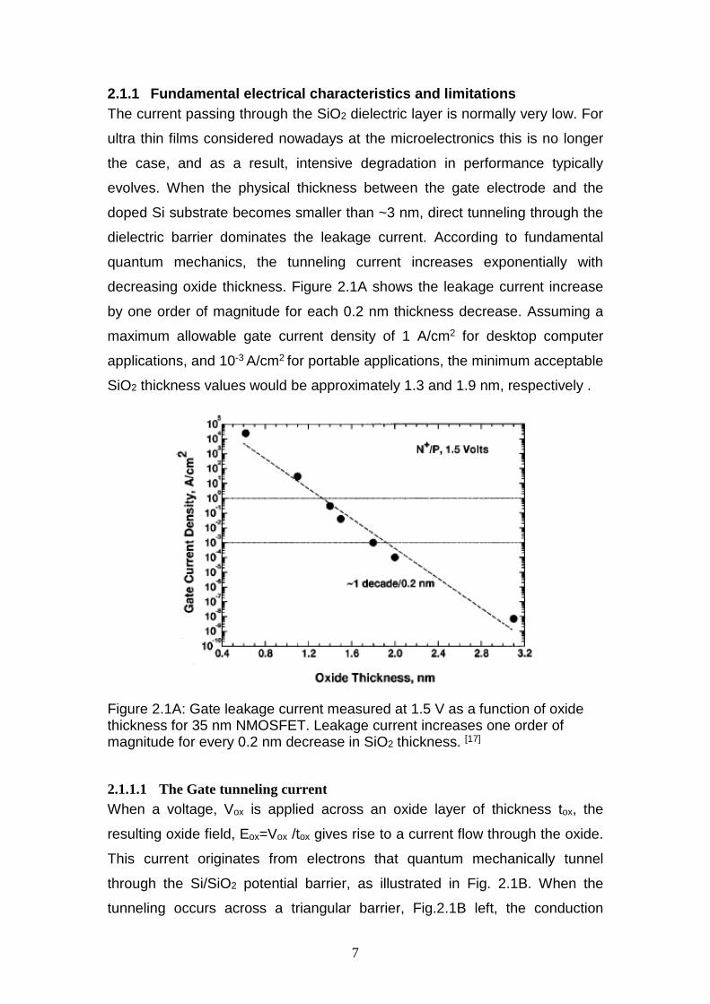
2.1.1 Fundamental electrical characteristics and limitations The current passing through the SiO2 dielectric layer is normally very low. For
ultra thin films considered nowadays at the microelectronics this is no longer
the case, and as a result, intensive degradation in performance typically
evolves. When the physical thickness between the gate electrode and the
doped Si substrate becomes smaller than ~3 nm, direct tunneling through the
dielectric barrier dominates the leakage current. According to fundamental
quantum mechanics, the tunneling current increases exponentially with
decreasing oxide thickness. Figure 2.1A shows the leakage current increase
by one order of magnitude for each 0.2 nm thickness decrease. Assuming a
maximum allowable gate current density of 1 A/cm2 for desktop computer
applications, and 10-3 A/cm2 for portable applications, the minimum acceptable
SiO2 thickness values would be approximately 1.3 and 1.9 nm, respectively .
Figure 2.1A: Gate leakage current measured at 1.5 V as a function of oxide thickness for 35 nm NMOSFET. Leakage current increases one order of magnitude for every 0.2 nm decrease in SiO2 thickness. [17]
2.1.1.1 The Gate tunneling current When a voltage, Vox is applied across an oxide layer of thickness tox, the
resulting oxide field, Eox=Vox /tox gives rise to a current flow through the oxide.
This current originates from electrons that quantum mechanically tunnel
through the Si/SiO2 potential barrier, as illustrated in Fig. 2.1B. When the
tunneling occurs across a triangular barrier, Fig.2.1B left, the conduction

8
mode is described by the Fowler–Nordheim (FN) model and the measured
current density, JFN , can be described by the expression:
1)
A and B are constants, where B is related to the electron effective mass in the
oxide conduction band
2)
where ϕ is the barrier height, q is the electron charge and m is its
Figure 2.1B: Schematic illustration of Fowler–Nordheim (left) and direct (right) tunneling mechanisms of electron flow though an oxide potential barrier of height ΦB[16] When the oxide voltage drops below 3.7V, electrons no longer enter the oxide
conduction band, but tunnel directly from the anode to the cathode , as
illustrated in Fig. 2.1B (right). In state-of-the-art CMOS technologies, direct
tunneling is the dominant current conduction mechanism at operating voltage,
and for oxide layers less than 3nm it is also the conduction mode for
accelerated oxide wear out and breakdown tests.

9
2.2 SiOF as low k dielectric in microelectronics process. Fluorinated silicon-dioxide is one of the low-k dielectric materials used to
reduce resistor–capacitor (RC) time delay and drive higher MOS device
speed. The incorporation of fluorine into SiO2 modifies the silicon–oxygen
matrix and results in a reduction of the dielectric constant that decreases with
increasing F content.
Fluorine incorporation into the SiO2 layer can be accomplished in several
ways which include HF rinses before gate oxidation, fluorine ion implantation,
and adding NF3 to O2 during gate oxidation. Another technique involves
Plasma Enhanced Chemical Vapor Deposition (PECVD) with SiF4 and O2 as
precursors.
Standard characterization techniques include FTIR for F content
determination and C-V for dielectric constant measurements. However, the
characterization of ultra-thin SiOF films, in terms of obtaining F concentration
and understanding where the F is located within the layer, has proven to be a
challenge. Fig. 2.2A showing a results of experiment performed by Byun and
Lee, which showing a clear relationship between %F in SiOF films as
measured using FTIR and the response of dielectric constant change using
MOS capacitor C-V curve.
Fig. 2.2A -Dielectric constant and %F response to SiF4/O2 ration change in PECVD[4]

10
2.3 C-V Characterization of Dielectric Thin Films. Maintaining the quality and reliability of gate oxides of MOS structures is a
critical task in a semiconductor Fab. Capacitance-voltage (C-V)
measurements are commonly used in studying gate-oxide quality in detail.
These measurements are made on a two-terminal device called a MOS
capacitor (MOS cap), which is basically a MOSFET without a source and
drain. C-V test results offer a wealth of device and process information,
including bulk and interface charges. Many MOS device parameters, such as
oxide thickness, flat band voltage, threshold voltage, etc., can also be
extracted from the C-V data.
Essentially, the MOS capacitor is just an oxide placed between a
semiconductor and a metal gate. The semiconductor and the metal gate are
the two plates of the capacitor. The oxide functions as the dielectric. The area
of the metal gate defines the area of the capacitor
The most important property of the MOS capacitor is that its capacitance
changes with an applied DC voltage. As a result, the modes of operation of
the MOS capacitor change as a function of the applied voltage. As a DC
sweep voltage is applied to the gate, it causes the device to pass through
accumulation, depletion, and inversion regions.
11
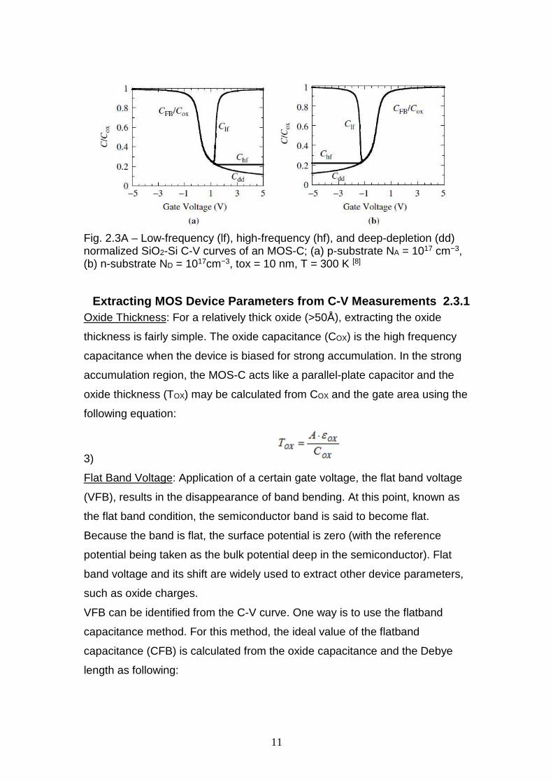
Fig. 2.3A – Low-frequency (lf), high-frequency (hf), and deep-depletion (dd) normalized SiO2-Si C-V curves of an MOS-C; (a) p-substrate NA = 1017 cm−3, (b) n-substrate ND = 1017cm−3, tox = 10 nm, T = 300 K [8]
2.3.1 Extracting MOS Device Parameters from C-V Measurements For a relatively thick oxide (>50Å), extracting the oxide : Oxide Thickness
cy high frequen) is the OXthickness is fairly simple. The oxide capacitance (C
capacitance when the device is biased for strong accumulation. In the strong
accumulation region, the MOS-C acts like a parallel-plate capacitor and the
and the gate area using the OXC) may be calculated from OXoxide thickness (T
following equation:
3)
: Application of a certain gate voltage, the flat band voltage Flat Band Voltage
(VFB), results in the disappearance of band bending. At this point, known as
the flat band condition, the semiconductor band is said to become flat.
Because the band is flat, the surface potential is zero (with the reference
potential being taken as the bulk potential deep in the semiconductor). Flat
band voltage and its shift are widely used to extract other device parameters,
such as oxide charges.
VFB can be identified from the C-V curve. One way is to use the flatband
capacitance method. For this method, the ideal value of the flatband
capacitance (CFB) is calculated from the oxide capacitance and the Debye
length as following:
12
:Effective and total bulk oxide charge
) represents the sum of oxide fixed charge EFFThe effective oxide charge (Q
):OT), and oxide trapped charge (QM), mobile ionic charge (QF(Q
monly ) is comMSsemiconductor work function difference (W-The metal
from the ideal FBreferred to as the work function. It contributes to the shift in V
zero value, along with the effective oxide charge. The work function
represents the difference in work necessary to remove an electron from the
gate and from the substrate. The work function is derived as follows:
2.4 Charged based and probe techniques
2.4.1 Introduction Many semiconductor characterization techniques are based on current,
voltage, and capacitance measurements. They generally require some device
fabrication or at least temporary contacts, e.g., mercury probe C–V
measurements. For example, to determine the oxide charge and interface trap

13
density of an MOS device, it is necessary to make an MOS capacitor,
traditionally done by evaporating a metal gate, depositing a poly-Si gate, or
using a mercury probe for the gate on an oxidized wafer. It is sometimes
useful to make measurements without device fabrication. One way is to
deposit charge on an oxidized wafer and measure the voltage contactless
with a Kelvin or Monroe probe. The charge in this configuration becomes the
“gate”. After all, applying a gate voltage to an MOS capacitor is equivalent to
placing a charge on the gate. Depositing the charge directly on the oxide
circumvents the gate formation with the additional advantage of being
contactless. The charge can be removed with a water rinse.
Charge-based measurements lend themselves to measurements during the
development of integrated circuits (ICs) and for manufacturing control. To be
effective, such test structures should provide rapid feedback to the pilot or
manufacturing line. Surface voltage (SV) and surface photovoltage (SPV)
semiconductor characterization techniques are suitable for such rapid
feedback and have become powerful and convenient methods for a variety of
material/device parameter measurements. The introduction of commercial
equipment led to widespread adoption by the semiconductor industry for
initially measuring the minority carrier diffusion length, later expanded to
encompass routine characterization of surface voltage, surface barrier height,
flatband voltage, oxide thickness, oxide leakage current, interface trap
density, mobile charge density, oxide integrity, generation lifetime,
recombination lifetime, and doping density. Charge, in these measurements,
is used in two basic ways: as the “gate” in MOS-type measurements, where
the charge replaces the metal or poly-silicon gate, and as a surface modifying
method, where the charge controls the surface potential. IBM developed
corona charge for semiconductor characterization during the period 1983–
1992. However, due to lack of commercial instruments, the technique was
initially only sparingly used. Later, it was developed into commercial products.
We give an introduction to this technique here, review the relevant theory and
compare the technique to the well-established MOS technique and illustrate it
with several examples.

14
2.4.2 Surface Charging Charge is deposited as a corona charge. Ions are deposited on a surface at
atmospheric pressure through an electric field applied to a source of ions. The
corona source consists of a wire, a series of wires, a single point, or multiple
points located a few mm or cm above the sample surface. The substrate may
be moved during charging or between charging cycles and the sample may
be charged uniformly or in well-defined areas through a mask. It is even
possible to deposit positive (negative) charge in a given area and surround
the area with negative (positive) charge, to act as a zero-gap guard ring.
A potential of 5,000–10,000 V of either polarity is applied to the corona
source, as
illustrated in Fig. 2.4A. Ions are generated close to the electrode, where a
faint glow may be observed in a darkened room. For a negative source
potential, positive ions bombard the source while free electrons are rapidly
captured by ambient molecules to form negative ions. For a positive source
potential, electrons are attracted to the source and positive ions follow the
electric field lines to the substrate. The negative and positive corona ionic
species are predominantly CO−3 and H3O+, respectively. The corona source
forces a uniform flow of ionized air molecules toward the surface. The very
short (approximately 0.1 µm) atmospheric mean free path of the ionized gas
ensures collision dominated ion transport with the molecules retaining very
little kinetic energy. Typically a few seconds are required to charge an
insulating surface to a saturation potential.
One of the advantages for oxide thickness and oxide integrity measurements
using corona charge “gates” rather than conductive gates is the low surface
mobility of the “corona” ions on the sample surface. A charge deposited on
the surface of an oxidized wafer, creates an oxide electric field. The oxide
breaks down at its weakest spot, with the current confined to the breakdown
spot, because the surface corona charge does not readily drift or diffuse along
the surface. By contrast, for a conductive gate with applied gate voltage, the
breakdown area may be the same as for the corona charge method, but the
current from the entire gate area will be channeled into the weak spot,
possibly leading to catastrophic breakdown.

15
Fig. 2.4A - Surface charge schematics of COS technique.[1]
2.4.3 Kelvin Probe How does a surface voltage or photovoltage come about and how is it
measured? A
surface voltage is generated by a surface or insulator charge or work function
difference and is most commonly detected with a non-contacting probe. The
probe is a small plate, 2–4 mm in diameter, held typically 0.1–1 mm above the
sample and vibrating with a constant frequency.
Fig. 2.4.B showing the schematic of Kelvin Probe surface potential
measurement. The voltage Vkp adjusted to vibrating Kevin Probe, until a “null”
current is achieved in a steady state. Vs then can be calculated from:

16
Fig. 2.4B – Oxide surface potential measurement configuration with Kelvin Probe
2.4.4 Applications
2.4.4.1 SPV Surface photovoltage was one of the first characterization techniques using
surface charge as discussed in section 2.4.2 and is commonly used to
determine the minority carrier diffusion length. The concept of surface
photovoltage can be understood with the band diagram in Fig. 2.4C. Surface
charge density Q induces charge density QS in the semiconductor with Q + QS
= 0 shown in Fig. 2.4C(a). The surface charge must be of a polarity to drive
the semiconductor into depletion. The band diagram in the dark is shown in
Fig. 2.4C(b). Incident light creates electron-hole pairs (ehps). Some ehps
recombine in the neutral p-substrate, some diffuse toward the surface. If they
reach the edge of the space-charge region (scr), the holes neutralize acceptor
atoms, thereby reducing the scr width and the electrons drift in the scr electric
field to the surface exchanging negatively electrons for negatively charged
acceptors. This generates a forward bias, reducing the band bending and
splitting the Fermi level into the quasi-Fermi levels φFn and φFp giving the
surface photovoltage VS = φFn − φFp in Fig. 2.4C(c). The SPV voltage, being
a surface voltage, is named VS here to be consistent with the nomenclature in
this chapter. For constant photon flux density _, the diffusion length is
extracted form a plot of 1/VS versus 1/α.

17
Fig. 2.4C (a) Cross-section with surface charge Q and semiconductor charge density Qs , (b) band diagram in the dark, (c) illuminated band diagram.[9]
2.4.4.2 Oxide Charge The surface voltage dependence on surface charge lends itself to
measurements of charge in the insulator on a semiconductor wafer or charge
on the wafer. This charge can be oxide charge, interface trapped charge,
plasma damage charge, or other charge.
A way to measure a net charge in the oxide layer which consist of Surface
charge (Qs), Mobile charge (Qm) Bulk trapped charge (Qot), interface trapped
charge (Qit) and fixed charge (Qf), is to deposit corona charge with
consecutive SPV measurement. As SPV crosses 0 value, a sum of deposited
corona charge equals the opposite net charge in the oxide, since it neutralize
it to establish Silicone flat band.
In addition, some charge separation can be established with the following
techniques:

18
For Qm measurements. First deposit positive corona charge, heat the wafer
to a moderate temperature of around 200◦C for a few minutes, driving the
mobile charge to the oxide-semiconductor interface. Cool the sample and
determine the flatband voltage VFB1 . Next repeat the procedure with a
negative corona charge and drive the mobile charge to the oxide-air interface
determining VFB2 . Qm is then determined by the flat band voltage difference
through the relation
Charge-based oxide charge measurements have an advantage over voltage-
based measurements. For example, to determine the oxide charge of an MOS
device one can measure the charge or the voltage. The relationship between
the oxide voltage uncertainty ∆Vox and oxide charge uncertainty ∆Qox is
9)
Suppose the oxide charge is determined from a voltage measurement with an
uncertainty of ∆Vox = 1 mV. ∆Qox varies from 2.2 × 10¹⁰ to 2.2 × 1011 cm−2
for oxide thicknesses from 10 nm to 1 nm. In voltage-based measurements,
there is a large uncertainty in oxide charge. For charge-based measurements,
there is a charge uncertainty, but that is independent of oxide thickness and is
on the order of ∆Qox/q = 109 cm−2 or less.
2.4.4.3 Oxide Thickness and Trap Density To determine the oxide thickness, corona charge density Q is deposited on
the oxidized wafer and the surface voltages are measured in the dark and
under intense light, giving the surface voltage VS, that is plotted versus
deposited charge density as in Fig. 2.4D

19
Fig. 2.4D - Surface voltage versus surface charge density for two oxide thicknesses.[1] In accumulation or inversion the curves are linear and the oxide thickness is
10)
This method is not subject to the poly-Si gate depletion effects of MOS-C
measurements. It is also not affected by probe punch through and is relatively
insensitive to oxide pinhole leakage currents. Interface traps distort the low-
frequency Clf − VS curve, as it is shown in Fig. 2.4E. Similarly, interface traps
distort the SPV − Q curve (Fig. 2.4F) and the interface trap density is
determined from that distortion.
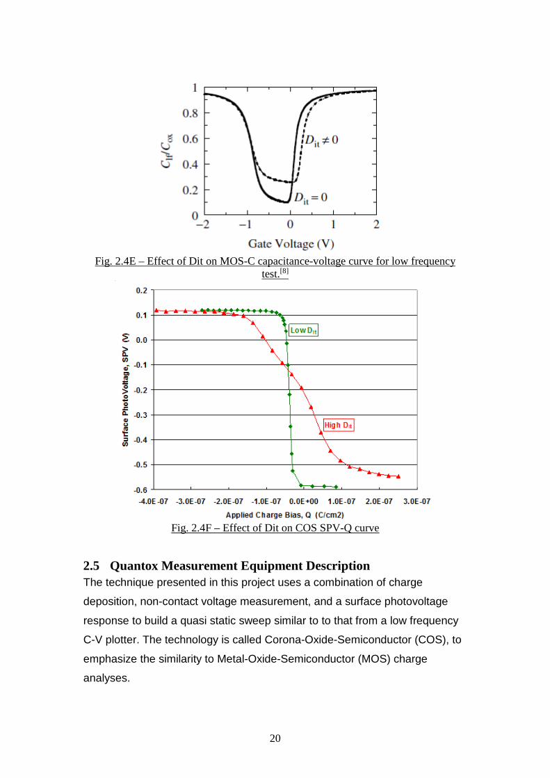
20
Fig. 2.4E – Effect of Dit on MOS-C capacitance-voltage curve for low frequency
test.[8]
Fig. 2.4F – Effect of Dit on COS SPV-Q curve
2.5 Quantox Measurement Equipment Description The technique presented in this project uses a combination of charge
deposition, non-contact voltage measurement, and a surface photovoltage
response to build a quasi static sweep similar to to that from a low frequency
C-V plotter. The technology is called Corona-Oxide-Semiconductor (COS), to
emphasize the similarity to Metal-Oxide-Semiconductor (MOS) charge
analyses.
21
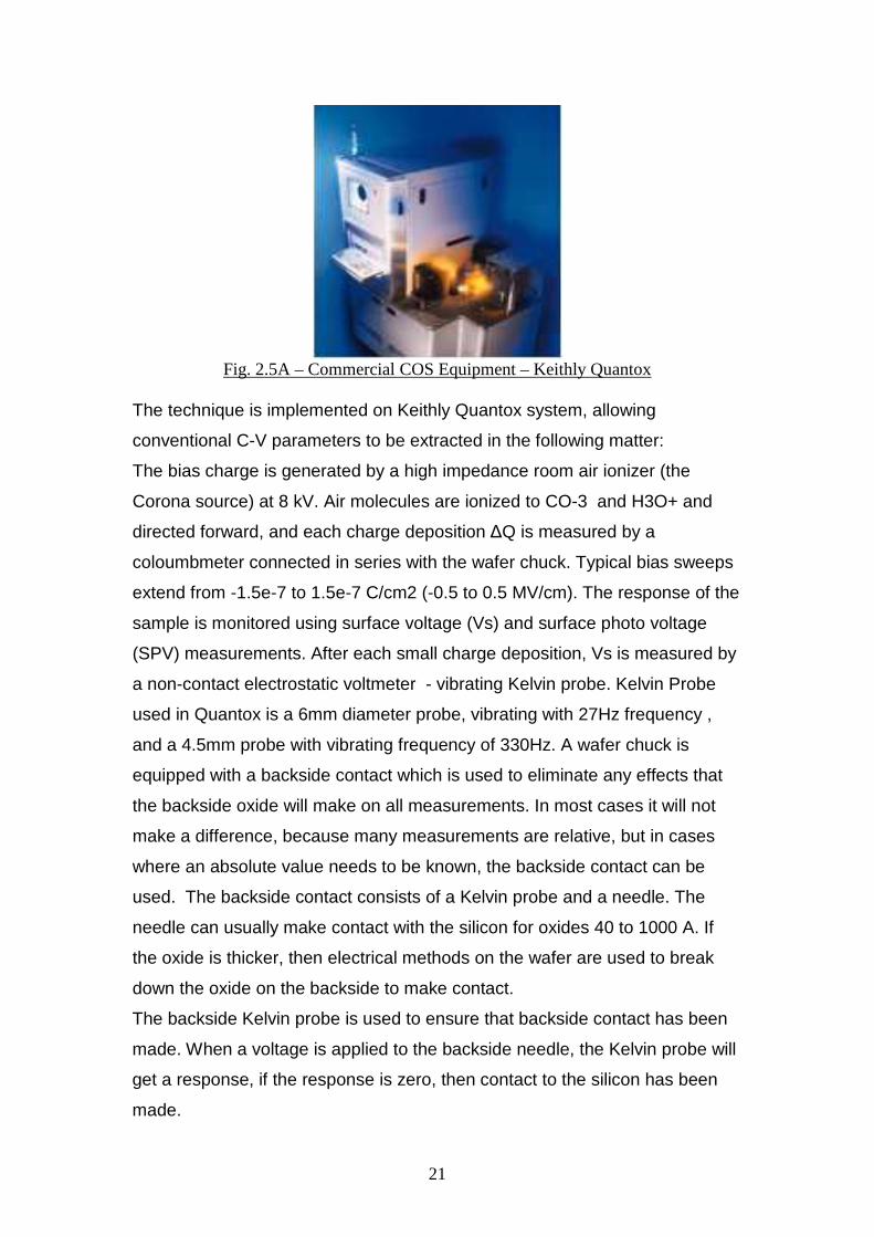
Fig. 2.5A – Commercial COS Equipment – Keithly Quantox
The technique is implemented on Keithly Quantox system, allowing
conventional C-V parameters to be extracted in the following matter:
The bias charge is generated by a high impedance room air ionizer (the
Corona source) at 8 kV. Air molecules are ionized to CO-3 and H3O+ and
directed forward, and each charge deposition ∆Q is measured by a
coloumbmeter connected in series with the wafer chuck. Typical bias sweeps
extend from -1.5e-7 to 1.5e-7 C/cm2 (-0.5 to 0.5 MV/cm). The response of the
sample is monitored using surface voltage (Vs) and surface photo voltage
(SPV) measurements. After each small charge deposition, Vs is measured by
a non-contact electrostatic voltmeter - vibrating Kelvin probe. Kelvin Probe
used in Quantox is a 6mm diameter probe, vibrating with 27Hz frequency ,
and a 4.5mm probe with vibrating frequency of 330Hz. A wafer chuck is
equipped with a backside contact which is used to eliminate any effects that
the backside oxide will make on all measurements. In most cases it will not
make a difference, because many measurements are relative, but in cases
where an absolute value needs to be known, the backside contact can be
used. The backside contact consists of a Kelvin probe and a needle. The
needle can usually make contact with the silicon for oxides 40 to 1000 A. If
the oxide is thicker, then electrical methods on the wafer are used to break
down the oxide on the backside to make contact.
The backside Kelvin probe is used to ensure that backside contact has been
made. When a voltage is applied to the backside needle, the Kelvin probe will
get a response, if the response is zero, then contact to the silicon has been
made.

22
Fig 2.5B - Quantox Backside contact schematics
Subsequent to a Vs measurement, a pulsed light source is directed at the
wafer. Quantox uses a Xenon bulb as a light source with wavelength range of
300nm-1500nm. The resultant surface SPV is coupled to the probe, and the
signal is analyzed to determine the silicon bend bending. The surface voltage
at SPV=0 is reported as the flat band voltage.
11)
Usage of SPV with a backside contact configuration, also allowing us to
deduce Vox values from Vs=Vox-SPV, based on following configuration (Fig.
2.5C)

23
Fig. 2.5C - Vox measurement from Vs and SPV combination with Backside contact.
Fig. 2.5D – Quantox Quasi-Static Q-V-SPV sweep
The amount of charge that is deposited to achieve the flat band condition is
defined as total oxide charge.
During the discrete charge deposition two plotes are generated, the Q-V plot
and Q-SPV plot. The first one allowing us to generate a low frequency C-V
plot by plotting surface voltage vs, dQ/dV (Fig 2.5F)
Fig. 2.5E – Q-V-SPV plots generated by Quantox

24
Fig 2.5F – Low frequency C-V plot calculated based on Quantox Q-V measurement
The oxide thickness (Tox) is extracted from the slope of the Q-V curve in
accumulation.
The Quantox tool may also be used to measure high filed oxide leakage. In
this application, bias charge density as high as 9e-6 C/cm2 are applied in
order to induce tunneling thru gate oxide. The maximum surface voltage is
clamped by tunneling of carriers through the oxide, and the tunneling field
may be calculated as following:
12)
Where WF is probe to silicone work function difference, and ΨSi is the band bending.
Fig 2.5G – Breakdown voltage measurement on Quantox Equipment

25
2.6 Ellipsometry Ellipsometry is a contactless, non-invasive technique measuring changes in
the polarization state of light reflected from a surface. It deals with intensity-
dependent complex quantities compared to intensities for reflectance or
transmittance measurements. Ellipsometry can be thought of as an
impedance measurement, while reflectance or transmittance can be viewed
as power measurements. Impedance measurements give the amplitude and
phase, whereas power measurements only give amplitudes. One determines
the complex reflection coefficient ratio of the sample that depends on the ratio
of the complex reflection coefficient for light polarized parallel and
perpendicular to the plane of incidence.
Ellipsometry is used predominantly to determine the thickness of thin
dielectric films on absorbing substrates, line width, and optical constants of
films or substrates. It does not measure the film directly, rather it measures
certain optical properties from which thickness and other sample parameters
are derived. Recent additions to basic Ellipsometry include variable angle and
variable wavelength (spectroscopic) Ellipsometry (SE), allowing thickness
measurements at least an order of magnitude smaller than interferometric
methods. Before going into the details of ellipsometry, it is important to
understand the properties of polarized light. When light is reflected from a
single surface it will generally be reduced in amplitude and shifted in phase.
For multiple reflecting surfaces, the various reflecting beams interact and give
maxima and minima as a function of wavelength or incident angle. Since
ellipsometry depends on angle measurements, optical variables can be
measured with great precision, being independent of light intensity,
reflectance, and detector-amplitude sensitivity.
Light propagates as a fluctuation in electric and magnetic fields at right angles
to the
direction of propagation (Fig 2.6A).

26
Fig. 2.6A
The total electric field consists of the parallel component Ep and the vertical
component Es . The reflection coefficients [7]
13)
are not separately measurable. However, the complex reflection ratio, ρ,
defined in terms of the reflection coefficients Rp and Rs or the ellipsometric
angles Ψ and ∆ is measurable and given by:
14)
The angles Ψ and ∆ determine the differential changes in amplitude and
phase, respectively, experienced upon reflection by the vibrations of the
parallel and perpendicular electric field vector components.
Ellipsometer schematic is shown in Fig. 2.6B

27
Fig. 2.6B Elliposmeter schematic.[7]
A common application of single wavelength Ellipsometry is in film thickness
measurements. But it can also be used for other applications, because the
ellipsometric angles Ψ and ∆ are sensitive not only to layer thickness, but also
to composition, microstructure, and optical constant of the sample surface.
Spectroscopic ellipsometric measurements have extended the range of
Ellipsometry by using more than one wavelength.
In this project I’ve used a commercially available, single wavelength Optiprobe
Elliposmeter equipped with 200mm silicon wafer handling system, produced
by Thermawave Inc. The measurement wavelength has been produced by
HeNe laser source of 633nm. Ellipsometry technique has been used as a
reference technique for thickness measurements, and as a complimentary
technique for dielectric constant calculation.
2.7 FTIR The foundations of modern Fourier Transform Infrared Spectroscopy (FTIR)
were laid in the latter part of the nineteenth century by Michelson and Lord
Raleigh who recognized the relationship of an interferogram to its spectrum by
a Fourier transformation.58 It was not until the advent of computers and the
fast Fourier algorithm that interferometry began to be applied to spectroscopic
measurements in the 1970s.

28
The basic optical component of Fourier transform spectrometers is the
Michelson interferometer shown in simplified form in Fig. 2.7A .Light from an
infrared source, a heated element or a glow bar, is collimated and directed
onto a beam splitter, creating two separate optical paths by reflecting 50% of
the incident light and transmitting the remaining 50%. In one path the beam is
reflected back to the beam splitter by a fixed position mirror, where it is
partially transmitted to the source and partially reflected to the detector. In the
other leg of the interferometer, the beam is reflected by the movable mirror
that is translated back and forth while maintained parallel to itself. The
movable mirror rides on an air bearing for good stability. The beam from the
movable mirror is also returned to the beam splitter where it, too, is partially
reflected back to the source and partially transmitted to the detector. Although
the light from the source is incoherent, when it is split into two components by
the beam splitter, the components are coherent and can produce interference
phenomena when the beams are combined.
The light intensity reaching the detector is the sum of the two beams. The two
beams
are in phase when L1 = L2. When M1 is moved, the optical path lengths are
unequal and an optical path difference δ is introduced. If M1 is moved a
distance x, the retardation is δ = 2x since the light has to travel an additional
distance x to reach the mirror and the same distance to reach the beam
splitter.

29
The detector output—the interferogram—consists of a series of maxima and
minima that can be described by the equation
15)
What is measured in FTIR is the interferogram, containing not only the
spectral information of the source, which we have considered so far, but also
the transmittance
characteristics of the sample. The interferogram, however, is of little direct
interest. It is the spectral response, calculated from the interferogram using
the Fourier transformation, that is of interest
16)
In This project I used FTIR as a reference technique for Fluorine content
measurement in SiOF film, according to what has been described in Section
2.2, Fluorine content have a direct impact on SiOF dielectric constant, the
purpose of FTIR measurements was to confirm dielectric constant change
measured by COS technique.
2.8 Project goals The goal of this project is to evaluate the COS technique for dielectric
properties characterization of simple and complicated dielectric stacks ranging
from simple SiO2 on p-type Si substrate to a complicated multi-layer dielectric
stack with various dielectric constants and composition. During this evaluation
we’ll evaluate the measurement capabilities and limitations of triple layer
SiO2-Si3N4-SiOF with various process conditions.
The project aims to evaluate the COS technique capability to be a
development and a process control technique of choice not only for a gate
oxide but also for a complicated stacks, replacing the complicated MOS
formation, thus decreasing the info-tern, and minimizing excursion impact on
production Fab.

30
3 Experimental settings
3.1 SiO2-Si3N4-SiOF Sample preparation All samples has been prepared on 200mm <100> P-Type Silicon wafer with B
doping concentration of 7E14, and resistivity of 10 [ohm-cm]. The wafers have
been pre-cleaned using SC1 for organic and airborne molecular contamination
removal with NH4OH+H2O+H2O2, and SC2 for metallic contamination
removal using H2O+H2O2+HCl at 25˚C for 10 minutes each. The purpose of
such a pre-clean is to assure quality interface between Si and SiO2, and
minimize interface trapped charge as well as metallic contamination on
sequential Q-V tests.
Following the pre-clean, the wafers have been oxidized at 900˚C in O2
environment at atmospheric pressure to form a 100A SiO2 layer. A reference
wafer has been “Dropped” for measurements using Ellipsometry and
Quantox, in order to provide a starting Tox for the following experiments. Next
sequence was a formation of thin Si3N4 layer using LPCVD at Kokusai Vertical
Diffusion furnace with NH3 and H2SiCl2 with pressure of 10[Pa] till a formation
of approximately 50A Si3N4 layer. Once again, a reference wafers have been
measured both using Ellipsometry and Quantox.
SiOF deposition has been performed on Applied Materials Ultima chamber
using HDPECVD technique with SiF4 and SiH4 and Ar as precursors, and 10
[mTorr] vacuum pressure. Due to HDP limitation of deposition rate control a
formation of an ultra thin layer wasn’t possible, so a very thick, 2000A layer
has been deposited during approximately 30 sec of deposition time, and the
etched backed at Wet etch process with HF and H2O at 1:50 ratio to a desired
thickness. In order to vary the dielectric constant, the F concentration in SiOF
films has been varied by SiF4 flow change in the range of 0 sccm to 26 sccm.
Eventually, all the samples have been measured by 3 different techniques
that have been described in section 2. For Q-V measurements Quantox
commercial equipment has been used.
Thickness and refractive index measurements have been performed using
KLA-Tencor Single Angle Spectroscopic Elliposmeter (SASE) in the
wavelength range of 193-800nm. The incident angle used for both UV and

31
visible spectrum was 65˚. In order to fit the data to physical model,
Generalized Lorenz Oscillator has been chosen. The extracted optical
properties along with film thickness have been verified using Beam Profile
Reflectrometry Method, by simultaneous measurement of Brewster angle and
film thickness at 633nm using HeNe laser.
Lorenz Oscillator material model can be used to model various material types
ranging from dielectrics to semiconductors. The Lorenz oscillator model works
well where other model might have a poor approximation, in particular where
anisotropic contribution of lattice is important. The general equation used for
Lorenz Oscillator is:
17)
Where:
m = Number of Oscillators. 3 Where chosen for SiOF, while 2 were chosen for
SiO2 and Si3N4.
ε∞ = High frequency lattice dielectric constant.
ECenter = the center energy of each oscillator given in eV.
A = the amplitude of each oscillator in eV.
ν = The vibration frequency of the “j” oscillator in eV.
At his project a more generalized form of Lorenz Oscillator have been used,
which included dumping coefficient, which unlike a classic Lorenz model that
assumes that all the oscillators are independent, allows coupling between the
oscillators. After fitting the model for materials dielectric constant, optical
properties have been extracted using a known relationship:

32
FTIR Spectra has been collected using Thermo-Nicolette FTIR equipment in
transmitted mode. Blanket Si wafer has been used as a background. Peak
intensities, area, and peak de-convolution has been performed using Thermo-
Nikolet commercial “Omnic” software.
4 Experimental Results
4.1 Spectroscopic Ellipsometry Results Table 4.1 summarizes the thickness results of various layers from the conducted experiment.
Layer Ellipsometry
Thickness [A] SiO2 100.1 Si3N4 58.3 SiOF 0% 990.5 SiOF 2% 970.2 SiOF 4% 890.4 SiOF 6% 820.7
results of dielectric stacks ThicknessTable 4.1: Spectroscopic Ellipsometry Figure 4.1A showing a linear dependency of %F content in SiOF film in
refractive index as being measured by the Ellipsometry tool at 673nm
wavelength.
content FluorineSiOF Refractive index dependence on –4.1A .Fig

33
4.2 FTIR Results Figures 4.2A-4.2C showing FTIR absorbance spectra for Si-O stretching, Si-F
stretching and Si-O bending modes respectively, with their dependence on
Fluorine concentration in SiOF film.
spectra FTIR O stretching mode absorbance-Si –4.2A .Fig
in SiOF film concentrationsF peak for various F -Si -4.2B .Fig

34
mode absorbance FTIR spectra bendingO -Si – C4.2 Fig.
deconvolution for 6% FluorineO peak -Si –Fig. 4.2D
Area FWHH Height Center Peak # 5.9480 45.4403 0.1083 1048.985 1 8.9806 45.2938 0.1627 1076.870 2 8.3920 37.2034 0.1825 1101.634 3
6% fluorine deconvolution summery –able 4.2A T

35
4% FluorineO peak deconvolution for -Si –Fig. 4.2D
Area FWHH Height Center Peak # 5.2225 44.3559 0.0975 1044.689 1 9.9806 48.3757 0.1700 1074.489 2 7.910 37.7026 0.1691 1101.544 3
% fluorine deconvolution summery4 –Table 4.2B
O peak deconvolution for 2% Fluorine-Si –Fig. 4.2E
Area FWHH Height Center Peak # 3.7488 41.9677 0.074 1038.630 1
11.2981 53.9682 0.1747 1070.540 2 7.2212 38.5271 0.1509 1101.329 3
% fluorine deconvolution summery2 – CTable 4.2

36
% Fluorine0O peak deconvolution for -Si – FFig. 4.2
Area FWHH Height Center Peak # 3.6491 42.4030 0.0717 1037.499 1 11.0948 54.8927 0.1689 1069.970 2 6.8876 38.5715 0.1437 1101.739 3
% fluorine deconvolution summery0 – DTable 4.2
Fig. 4.2G Peak 2 FWHH dependence on Fluorine concentration.

37
4.3 Q-V-SPV Measurement Results SiO2 (Padox) on Si Quantox measurements
Fig. 4.3A Quantox C-V plot for SiO2 on Si
Fig. 4.3B Quantox Q-V plot for SiO2 on Si

38
Fig. 4.3C Quantox Q-V-SPV plot for SiO2 on Si
Thin Si3N4 (TiNi) on Padox Quantox measurement results
39
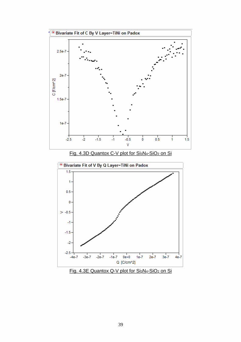
Fig. 4.3D Quantox C-V plot for Si3N4-SiO2 on Si
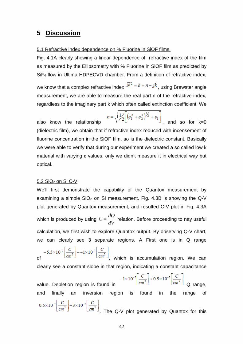
Fig. 4.3E Quantox Q-V plot for Si3N4-SiO2 on Si

40
Fig. 4.3F Quantox Q-V-SPV plot for Si3N4-SiO2 on Si
Fig. 4.3G Quantox C-V plot for SiOF-Si3N4-SiO2 on Si

41
Fig. 4.3H Quantox Q-V plot for SiOF-Si3N4-SiO2 on Si
Fig. 4.3K Quantox Q-SPV plot for SiOF-Si3N4-SiO2 on Si
42
5 Discussion
5.1 Refractive index dependence on % Fluorine in SiOF films.
Fig. 4.1A clearly showing a linear dependence of refractive index of the film
as measured by the Ellipsometry with % Fluorine in SiOF film as predicted by
SiF4 flow in Ultima HDPECVD chamber. From a definition of refractive index,
we know that a complex refractive index , using Brewster angle
measurement, we are able to measure the real part n of the refractive index,
regardless to the imaginary part k which often called extinction coefficient. We
also know the relationship , and so for k=0
(dielectric film), we obtain that if refractive index reduced with incensement of
fluorine concentration in the SiOF film, so is the dielectric constant. Basically
we were able to verify that during our experiment we created a so called low k
material with varying ε values, only we didn’t measure it in electrical way but
optical.
5.2 SiO2 on Si C-V
We’ll first demonstrate the capability of the Quantox measurement by
examining a simple SiO2 on Si measurement. Fig. 4.3B is showing the Q-V
plot generated by Quantox measurement, and resulted C-V plot in Fig. 4.3A
which is produced by using dV
dQC = relation. Before proceeding to nay useful
calculation, we first wish to explore Quantox output. By observing Q-V chart,
we can clearly see 3 separate regions. A First one is in Q range
of , which is accumulation region. We can
clearly see a constant slope in that region, indicating a constant capacitance
value. Depletion region is found in Q range,
and finally an inversion region is found in the range of
. The Q-V plot generated by Quantox for this

43
measurement fairly agrees with expected output from the literature as
explained in section 2.4, and pronounced in Fig. 2.4D.
When examining the resulted C-V plot, we can find that the average
Capacitance in accumulation region is found to
be . By using a relationship , where
ε0=8.8541[F/m], and k=3.9 for SiO2, we receive that Tox = 103.4 [A], which is
in excellent agreement with Ellipsometry measurement as presented in Table
4.1 and equals to 100.1 [A]. The 3.3 [A] offset which are 3.3%, are resulted
from various factors.
1. Quantox measurement error which is estimated as 0.3A based on
repeatability test of the system.
2. True dielectric constant of the SiO2 which defers from theoretical k=3.9.
If we’ll use Ellipsometry as an absolute reference to calculate a true k,
we receive
3. Finally The Ellipsometric measurement itself can produce some errors,
although much smaller then Quantox measurement. The main error in
Ellipsometric result is induced by refractive index used for the
measurement model. For the entire experiment I used n = 1.458, which
is a refractive index of perfect thermal SiO2, any variation from this
value will be resulted in thickness shift.
Overall, we can summarize that comparison of Electrical Q-V measurement to
optical Ellipsometry measurement of oxide thickness, produced a fairly similar
results with only 3% deviation. We’ll use this important conclusion when we’ll
calculate the k of low k SiOF films with varying Fluorine content.
5.3 SiO2 on Si Q-V-SPV
Examining further the SiO2-Si Q-V-SPC plots we can find additional useful
information for our dielectric stack characterization. First, from observing the
SPV charts, we can confirm the accumulation-depletion-inversion regions for
P-Type Si. In accumulation, when sample surface is being illuminated, an
electrons diffuse to the surface thus producing positive voltage as measured
by Kelvin probe. That voltage is constant thru entire accumulation region. In
44
inversion, the voltage is opposite, since from electron-hole pairs created by
illumination, only holes diffuse to the surface thus producing opposite voltage.
In depletion region, we see a SPV change as a function of depletion area
length, in curtain point, we are able to detect SPV=0 point. In this point either
charged diffused thru the surface after electron-hole pair creation, thus there
is no electric field at the Si surface, meaning that the surface is in flat band
condition. By measuring Surface voltage sequential to SPV=0, we are able to
find a flat band voltage of our dielectric stack, in this SiO2-Si stack case, the
flat band voltage VFB=VSPV=0=-0.435[V].
Additional useful information that can be extracted from Q-V-SPV
measurement, is the total amount of charge found in the oxide. Although this
type of measurement will not be able to distinguish between the various
charge type as described in section 2.4, it is somewhat useful to be able to
track the total amount of charge in the oxide layer, for process control
purposes[3]. The total amount of charge in the oxide layer can be found as
inverse of total amount of charge deposited by corona on oxide surface, until
a flat band conditions are reached :
.
5.4 Si3N4-SiO2 on Si C-V measurements.
An equivalent electrical circuit of Si3N4-SiO2-Si can be described as
following:
Fig. 5.4A – Equivalent circuit of Si3N4-SiO2 stack
In order to calculate the thickness of Si3N4 Layer in the stack, we’ll calculate
the total capacitance
4N3Si
2OSi

45
From the C-V plot for Si3N4-SiO2-Si stack – Fig. 4.3D, we can see that the
total Capacitance in accumulation region :
The resulted k for Silicon-nitride layer, 5.96 is significantly lower than value of
8 found in literature [15]. This is due the following reason: In our calculation of
Si3N4 thickness we neglected the interface layer between Si3N4 and SiO2, this
is not true, and in fact the equivalent electrical circuit should be as following:
Fig. 5.4B – Equivalent circuit of Si3N4-SiO2 stack with interface impact
However, since our Quantox measurement is equivalent to low-frequency C-V
measurement, we cannot distinguish between the interface capacitance and
Silicon-Nitride capacitance, so the Si3N4 k that we found is actually the
equivalent k of the silicon nitride and nitride to oxide interface layer. Since our
final goal is to calculate the low k of the following SiOF layer, such equivalent
є is still satisfying our needs, but this disadvantage of Quantox measurement
is clearly seen.
5.5 Si3N4-SiO2 on Si Q-V-SPV measurements.
4N3Si
2OSi
2OSi -4N3Si

46
In similar matter that we’ve observed the Q-V-SPV plots for SiO2 on Si,
Figures. 4.3E and 4.3F showing the Q-V-SPV curves for the Si3N4 – SiO2 – Si
stack.
The contribution of the nitride layer to the total charge is very significant, and
resulting from dangling bonds in Si3N4-SiO2 interface, and defects inSi3N4
matrix in comparison to a thermally grown SiO2 on Si
VFB of entire stack is shifted by 0.734 [V] comparing to SiO2 on Si, due to 2
contributing factors:
1. Total charge increase in the dielectric stack as indicated by QTotal
result.
2. Charge distribution in the dielectric stack. The majority of charge is
located in Nitride-Oxide interface and in the Nitride layer. From the
expression :
we can see that VFB dependence on geometrical factor and charge
density as function of thickness and not only the amount of charge.
This results pointing to a very important advantage of COS technique
with regarding to the traditional MOS C-V, and that is the fact that the
total amount of charge in the dielectric layer can be measured
independently to flat band voltage, thus providing the additional
information of not only the amount of charge, but also where it is
located.
This feature is especially important when dealing with stacks and
inhomogeneous layers.

47
Fig. 5.5A – Charge distribution in dielectric layer and it’s impact on Flat Band
Voltage.
5.6 SiOF-Si3N4-SiO2 on Si C-V curves.
Before reviewing the Quantox results of SiOF-Si3N4-SiO2 stack, I’d like to point
a several practical difficulties associated with SiOF electrical measurements.
Those difficulties are common to COS and MOS measurement techniques,
and had inherited impact on measurement results.
1. Direct deposition of SiOF on Si is impossible due to Sputter-Deposition
sequence of HDPECVD Applied Materials Ultima Chamber. Initial
sputtering of Argon ions induce damage to Si surface, making both
COS and MOS measurements impossible. To overcome this problem,
there is a need to deposit protective layer first. In our project, one of
the purposes of Si3N4 and SiO2 was So protection from sputter step,
although this was not a sole role of that stack.
2. Variation in Fluorine content in SiOF films, dramatically impact on both
the deposition rate in Ultima chamber, and Wet etch rate HF and H2O
at 1:50 ratio. Those factors made the mission of targeting the various
experiment samples to same thickness almost impossible, especially
due to the fact that all the experiments were held in production Fab
with limited access to the production equipment.
Fig. 4.3G is showing a C-V plot based on Quantox Q-V-SPV output. From the
C-V curve we can clearly see the dependence of Capacitance values vs. the
optical thickness as measured by Ellipsometry.

48
Fig. 5.6A – Capacitance dependence on SiOF film thickness as measured by
Quantox
The Si3N4 and SiO2 thickness values have been kept constant for all samples,
due to a very good thickness control in vertical diffusion surface, so we can
assume with high confidence that all the changes that observed in C-V plots
related to top SiOF layer only.
5.7 SiOF dielectric constant calculation
Let us describe the equivalent electrical circuit again, this time including SiOF
layer
4N3Si
2OSi
2OSi -4N3Si
SiOF 4N3iS -OFSi
49
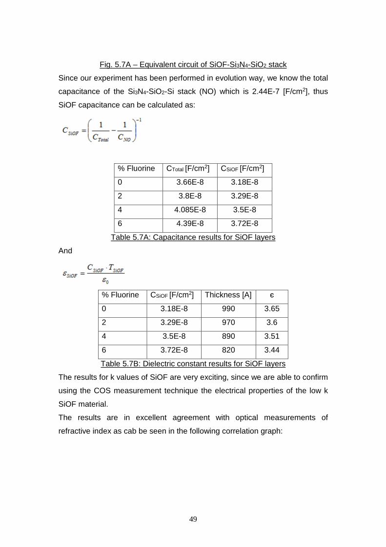
Fig. 5.7A – Equivalent circuit of SiOF-Si3N4-SiO2 stack
Since our experiment has been performed in evolution way, we know the total
capacitance of the Si3N4-SiO2-Si stack (NO) which is 2.44E-7 [F/cm2], thus
SiOF capacitance can be calculated as:
% Fluorine CTotal [F/cm2] CSiOF [F/cm2]
0 3.66E-8 3.18E-8
2 3.8E-8 3.29E-8
4 4.085E-8 3.5E-8
6 4.39E-8 3.72E-8
Table 5.7A: Capacitance results for SiOF layers
And
% Fluorine CSiOF [F/cm2] Thickness [A] є
0 3.18E-8 990 3.65
2 3.29E-8 970 3.6
4 3.5E-8 890 3.51
6 3.72E-8 820 3.44
Table 5.7B: Dielectric constant results for SiOF layers
The results for k values of SiOF are very exciting, since we are able to confirm
using the COS measurement technique the electrical properties of the low k
SiOF material.
The results are in excellent agreement with optical measurements of
refractive index as cab be seen in the following correlation graph:

50
Fig. 5.7B – Refractive index vs. SiOF dielectric constant correlation
As expected the dependence of є in refractive index is parabolic from the
expression є=N2 as described in section 3.1
The results also have a good agreement with literature confirming that
Flouring content increase resulting in dielectric constant decrease [4].

51
6 Summary
In this project I evaluated a Corona-Oxide-Semiconductor dielectric
characterization technique, as alternative to traditional MOS technique.
The COS has a clear advantage of being able to implement the measurement
in production line with rapid feedback to line performance.
Several points of interest has been evaluated in this project:
1. Ability to measure single thin dielectric film has been demonstrated y
Quantox measurement of thermal SiO2 layer on P-type Silicon.
2. Ability to measure dielectric stacks and to conclude from the total
capacity measured the thickness of each individual layer in the stack.
That was demonstrated by Si3N4-SiO2-Si stack measurement,
although a clear disadvantage has been found, in that that due to quasi
low-frequency measurement, COS technique is incapable to separate
between the layer and the inter-layer interface capacitance.
3. A Total charge in dielectric stack has been demonstrated along with
Flat-Band voltage measurement, by incorporating SPV technique to
charge-surface voltage measurement. A great advantage has been
found during that demonstration to COS technique over a traditional
MOS, due to ability of separately measure the charge amount and the
flat band voltage.
4. The ability of Dielectric constant measurement has also been
demonstrated, by combination of COS with independent thickness
measurement of dielectrics, by a conventional ellipsometric
measurement. The ability to combine COS and Ellipsometry, providing
very powerful tools to process engineer in low/high k dielectrics
fabrication process control. We demonstrated the ability to measure
dielectric constant of low k material SiOF, with excellent agreement to
theory and to literature.
COS technique holding a large potential in addition to what was dealt in this
project, those include breakdown voltage measurement, Si Contamination
and Doping, Mobile charge measurement and SiO2-Si interface
characterization. Last one is possible by exploring the depletion region of the
C-V or Q-V curve. Although my project has been dealing especially with

52
accumulation region due to specific interest of dielectric constant
measurement, I’d suggest to continue COS characterization with
concentration on interfaces states.
7 List of shortcuts C-Capacitance
Q - Charge
V-Voltage
SV-Surface Voltage
SPV – Surface Photo Voltage
KP-Kelvin Probe
COS-Corona Oxide Semiconductor
MOS – Metal Oxide Semiconductor
FTIR – Fourier Transformer Infra Red
SE – Spectroscopic Ellipsometry
RI – Refractive Index.
Tox – Oxide Thickness.
Vfb – Flat Band Voltage
Qtot – Total Charge
Dit – Interface trapped charge density.
є- dielectric constant.
n - refractive index.
k – extinction coefficient.

53
8 References
1. Semiconductor material and device characterization 3rd edition – Dieter
K. Schroder, Wiley & Sons, 2006.
2. R.G Cosway, K.B Catmull, Manufacturing implementation of corona-
oxide-semiconductor systems for diffusion furnace contamination
monitoring, IEEE(1997)
3. R.G Cosway, K.B Catmull, Uses of Corona-Oxide-Silicon measurement
for diffusion process monitoring and troubleshooting, IEEE(1998)
4. K.M Byun, W.J Lee, Deposition characteristics of low dielectric
constant SiOF films prepared by ECR PECVD. Metals and Materials 6-
2, 155-160 (2000).
5. P.K Roy, C.S Horner, Non-Contact characterization of ultra-thin
dielectrics for the gigabit Era, Keithly technology paper (1997)
6. B. Letherer, R.G Cosway, Control of nitrogen incorporation in tunnel
oxides using in-line non contact electrical characterization. Elect.
Society Meeting (1998)
7. Spectroscopic Ellipsometry and Reflectrometry, H.G Tompkins, W.A
McGahan, Wiley & Sons, 1999
8. MOS Physics and Technology, E.H.Nicollian, Wiley & Sons, 1982
9. L. Kronik and Y. Shapira, “Surface Photovoltage Phenomena: Theory,
Experiment, and Applications”, Surf. Sci. Rep. 37, 1–206, Dec. 1999.
10. D.K. Schroder, M.S. Fung, R.L. Verkuil, S. Pandey, W.H. Howland,
and M. Kleefstra, “Corona- Oxide-Semiconductor Device
Characterization,” Solid-State Electron. 42, 505–512, April 1998.
11. D.K. Schroder, “Surface Voltage and Surface Photovoltage: History,
Theory and Applications,” Meas. Sci. Technol. 12, R16–R31, 2001
12. B.E. Deal, “Standardized Terminology for Oxide Charges Associated
with Thermally Oxidized Silicon,” IEEE Trans. Electron Dev. ED-27,
606–608, March 1980.
13. W.E. Beadle, J.C.C. Tsai and R.D. Plummer, Quick Reference Manual
for Silicon Integrated Circuit Technology, Wiley-Interscience, New
York, 1985, 14–28.

54
14. G. Horlick, “Introduction to Fourier Transform Spectroscopy,” Appl.
Spectrosc. 22, 617–626, Nov./Dec. 1968.
15. E.A Joseph, C. Gross, Characterization of Si-rich nitride and oxynitride
films for polysilicon gate patterning, J. Vac. Sci. Technology, A19(5)
2001.
16. M. L. Green, E. P. Gusev, R. Degraeve, and E. L. Garfunkel, J.
Appl. Phys. 90, 2057-2121 ,(2001).
17. J. P. Chang, M. L. Green, V. M. Donnelly, R. L. Opila, J. Eng, J.
Sapjeta, P. J. Silverman, B. Weir, H. C. Lu, T. Gustafsson, and
E. Garfunkel, J. Appl. Phys. 87, 4449, (2000).