digital bat ears proposal - makerspace...
TRANSCRIPT

1
Digital Bat Ears
ECE 445 Design Review
Paul Logsdon
Ian Bonthron
Group #32
TA: Kevin Chen

2
Table of Contents
1.0 Introduction 3
1.1 Statement of Purpose 3
1.2 Objectives 3
1.2.1 Goals 3
1.2.2 Functions 3
1.2.3. Features 3
1.2.4 Benefits 4
2.0 Design 4
2.1 Block Diagram 4
2.2 Block Descriptions 4
3.0 Requirements and Verification 24
4.0 Tolerance Analysis 27
5.0 Cost Analysis and Schedule 28
5.1 Labor Cost Analysis 28
5.2 Parts Cost Analysis 29
5.3 Schedule 30
6.0 Ethics and Safety 31
7.0 References 32

3
1.0 Introduction
1.1 Statement of Purpose:
The goal of this project is to develop a full spectrum bat detector at a reasonable cost. This
device will record bat calls up to 100 KHz, downshift the calls into the human hearing range (20
Hz-20 KHz), and play the calls back through an audio jack without seriously distorting the signal.
Also, the device will store the processed/original data for further processing on an SD card and
provide an intuitive interface to the user. Bat detectors currently available on the market
which have this functionality range from $500-$1000. We aim to provide similar functionality
but only using $50-$100 worth of parts.
1.2 Objectives:
1.2.1 Goals:
1. Characterize a variety of MEMS microphones to determine their sensitivity in the
ultrasonic range.
2. Based on the information from (1), design an amplifier/filter stage based on the
empirical frequency response of said microphones.
3. Develop algorithms to compress/downshift ultrasonic data into the human hearing
range and implement on a microcontroller.
4. Develop UI to interact with microcontroller.
5. Develop algorithms to store data from microcontroller to SD card
1.2.2 Functions:
1. Records audio in the ultrasonic range (up to 100 KHz)
2. Downshifts audio and plays it back through the headphone jack.
3. Saves raw and/or downshifted data to the SD card
4. Provides user interface to repeat or delete different recordings
1.2.3 Features:
1. Contains a MEMS ultrasonic microphone for low cost, high accuracy recording
2. Contains a low power TI microcontroller for fast and efficient processing
3. Powered by standard AA batteries
4. Interfaces with standard 3.5 mm headphones and SD cards

4
5. Electronics are stored in a durable case
1.2.4 Benefits:
1. Provides advanced functionality at a low cost
2. Has a friendly and intuitive UI
3. Provides output in a format which can be easily analyzed on a PC
4. Durable and portable
2.0 Design
2.1 Block Diagram:
2.2 Block Descriptions:
Ultrasonic Microphone
Input Output
Sound from outside environment, which will include ultrasonic bat calls.
AC voltage limited between 0 and 1 V (ideally) which represents the ultrasonic sound.
The device we have chosen for our ultrasonic microphone is the Knowles SPQ0410HR5H-B. This

5
is a MEMS microphone which has sensitivity in the ultrasonic range, which suits our purposes.
One challenge that this device (as well as all available MEMS microphones) bring is that it has
contacts only on the bottom of the package, as shown in Figure 2.1. A custom PCB must be
created to specifically test and later use the device. In addition, a reflow oven (or similar
process) must be used to solder the device according to the given soldering profile, as shown in
Figure 2.2.
The microphone has a sensitivity of -42 dBV/Pa (measured at 1 kHz), which means that the
voltage from the microphone actually decreases with increases in sound volume.
Figure 2.1 – Microphone packaging

6
Figure 2.2 – Reflow Profile

7
Figure 2.3 – microphone pin-out
Band Pass Filter
Inputs Outputs
Raw analog data from microphone. Isolated ultrasonic calls

8
In order to hear the ultra-sonic frequencies, we implemented a band pass filter to dampen the
undesired frequencies. We ultimately decided to a single staged, passive filter. The Butterworth
filter had too much gain in cutoff frequencies, and Chebychev filter did not enough total loss to
satisfy the needs of the filter. Since our big concern is the lower frequencies, the inductor was
used a shunted the high impedance. The rest of the circuit was model as a 50 ohm resistor.
From the data sheet of the microphone, the source impedance was read to be 400 ohms. Using
this data we set up our circuit simulations. Figure 2.4 shows the current layout chosen for the
filter. After laying it out in ADS, Figure 2.5 shows the simulated frequency response.
Figure 2.4(above) Figure 2.5 (left)
Input Amplifier
Inputs Outputs
Isolated ultrasonic bat calls (after filtering).
Voltage between 0 and 3.3 V, which is the full range of values for the A/D converter.

9
An amplifier used to amplify signals from the microphone to levels required for the analog to
digital converter. The ADC has an input limit of 3.3V (for voltage values greater than or equal to
3.3V, ADC will convert it to the maximum value of 4095). Based on the 0-1 V range of the
microphone and this requirement, we have designed a non-inverting op-amp circuit which will
do the necessary amplification. The schematic for this device is given below in figure 2.6.
Figure 2.6 – Input Amplifier Schematic
This device has a gain given by the equation:
𝑉𝑜𝑢𝑡 = (1 − 𝑉𝑖𝑛)𝑅2/𝑅1
With R2 = 3.3k ohms and R1 = 1k ohm, the device obtains a gain of 3.3. With the input voltage
limited between 0-1 V, our output is thus limited between 0-3.3 V. Also, the coupling capacitor
was chosen based on the recommendation given in the SiSonic Design Guide (see references).

10
Analog to Digital Converter
Inputs Outputs
Ultrasonic bat calls, filtered and amplified to the correct level.
12 bit digital data representing the bat calls, which will be sent to the microcontroller for processing.
The Analog to Digital Converter we’ve chosen is built-in to our microcontroller as a peripheral.
It operates at 1 MSPS (one million samples per second or 1 MHz). With an upper limit of 100
KHz on our input signal, this allows us to oversample at 10x, which is ideal. This ADC has a
resolution of 12 bits, which provides 212-1 = 4095 levels.
Microcontroller
Inputs Outputs
Digital bat call data from ADC
User interface information from push buttons
Stored data on SD card via serial connection
Program information via USB connection
Downshifted and compressed audio data will be sent to DAC
Raw data to be saved on SD card, via serial connection
UI information via serial connection to LCD
The microcontroller we’ve chosen is the Tiva TM4C123GH6PM. As the heart of the system, it is
responsible for a great number of things, and connects to many different components. A pin diagram,
as well as a pin table, given below in Figures 2.7 and 2.8, illustrate this.

11
Figure 2.7 – Microcontroller Pin Diagram
Pin(s) Description Connections
2,11,26,42,54 Vdd/VddA pins Connect to +3.3 V power supply
3,12,27,39,55 Ground pins Connect to GND
17 GPIO/SPI Use for SD card I/O
18 GPIO/SPI Use for serial interface with LCD display
19-22,47-49 GPIO Use with push buttons
6 ADC Input Connect to output of amplifier/filter stage
52 GPIO Send data serially to digital to analog converter
45-46 USB Connect to USB plug
25,56 Vddc Connect to +1.2 V power supply
Figure 2.8 – Microcontroller Pin Table

12
The microcontroller will be responsible for converting the bat calls in the 20 kHz to 100 kHz
range into the human hearing range of 20 Hz to 20 kHz. A couple of algorithms and their
MATLAB simulations are given below as two different ways to do this.
Frequency Shifting/Compression Algorithms
The first method is the time expansion method. It is precise, but is not an algorithm that can be
done in real time. This is because the amount of memory used by the program will grow
without bound.
%this code implements the time expansion method of compressing a frequency
%range. This is the ideal method since it is very precise. However this
%is not an algorithm intended for real time processing
Fs = 5e5; %sampling rate of 500 kHz
T = 1/Fs; %normal period calculation
L = 10000; %length of FFT
t = (0:L-1)*T; %time vector
% show initial signal's FFT
x1=0;
F = [1e5,2e4,8e4,8.9e4,9e4];
for i=F
x1 = x1 + sin(2*pi*i*t);
end
%
F = [1e5,8.1e4,8e4];
for i=F
x1 = x1 + sin(2*pi*i*t);
end
%
%
F = [1e5];
for i=F
x1 = x1 + sawtooth(i*t);
end
%
lenFFT = 2^nextpow2(L);
figure(1);
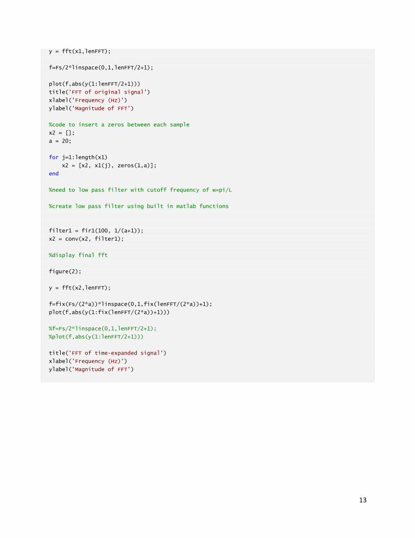
13
y = fft(x1,lenFFT);
f=Fs/2*linspace(0,1,lenFFT/2+1);
plot(f,abs(y(1:lenFFT/2+1)))
title('FFT of original signal')
xlabel('Frequency (Hz)')
ylabel('Magnitude of FFT')
%code to insert a zeros between each sample
x2 = [];
a = 20;
for j=1:length(x1)
x2 = [x2, x1(j), zeros(1,a)];
end
%need to low pass filter with cutoff frequency of w=pi/L
%create low pass filter using built in matlab functions
filter1 = fir1(100, 1/(a+1));
x2 = conv(x2, filter1);
%display final fft
figure(2);
y = fft(x2,lenFFT);
f=fix(Fs/(2*a))*linspace(0,1,fix(lenFFT/(2*a))+1);
plot(f,abs(y(1:fix(lenFFT/(2*a))+1)))
%f=Fs/2*linspace(0,1,lenFFT/2+1);
%plot(f,abs(y(1:lenFFT/2+1)))
title('FFT of time-expanded signal')
xlabel('Frequency (Hz)')
ylabel('Magnitude of FFT')

14

15
The second method is an averaging method. It does not give the ideal results but it can be
done in real time.
%this code implements the approximation method. This
%method is not precise but can be done in real time
Fs = 5e5; %sampling rate of 500 kHz
T = 1/Fs; %normal period calculation
L = 10000; %length of FFT
t = (0:L-1)*T; %time vector
% show initial signal's FFT
x1 = 0;
F = [1e5,2e4,8e4,8.9e4,9e4];
for i=F
x1 = x1 + sin(2*pi*i*t);
end
%
F = [1e5,8.1e4,8e4];
for i=F
x1 = x1 + sin(2*pi*i*t);
end
%
%
F = [1e5];
for i=F
x1 = x1 + sawtooth(i*t);
end
%
lenFFT = 2^nextpow2(L);
figure(3);
y1 = fft(x1,lenFFT);
f=Fs/2*linspace(0,1,lenFFT/2+1);
plot(f,abs(y1(1:lenFFT/2+1)))
title('FFT of original signal')
xlabel('Frequency (Hz)')
ylabel('Magnitude of FFT')
%build new frequency spectrum by averaging technique

16
a=20;
y2 = zeros(1,lenFFT/2+1);
for i = 1 : a : lenFFT/2+1
j = i:i+a;
if and((f(i) >= 2e4),(f(i) <= 1e5))
y2(fix(i/(a+1))) = mean(y1(j));
end
end
figure(4)
f=fix(Fs/(2*a))*linspace(0,1,fix(lenFFT/(2*a))+1);
plot(f,abs(y2(1:fix(lenFFT/(2*a))+1)))
%f=Fs/2*linspace(0,1,lenFFT/2+1);
%plot(f,abs(y(1:lenFFT/2+1)))
title('FFT of modified signal using average method')
xlabel('Frequency (Hz)')
ylabel('Magnitude of FFT')

17
User Interface
In addition to performing the previously mentioned signal processing, the microcontroller will
also work with the LCD and push buttons to provide a user interface. A state diagram for this
user interface is given below in Figure 2.9. See the LCD and push button sections for more
information about these parts and how the contribute to the user interface.

18
Figure 2.9 – User Interface state diagram
Digital to Analog Converter
Input Output
Processed digital audio data from microcontroller
Analog voltage to be send to output amplifier. From 3.3V to 0V.
The digital to analog converter we’ve chosen to use is the Maxim Integrated MAX5216BGUA+.
This device can operate at frequencies up to 50 MHz. Our output from the DAC is going to be
limited to the human hearing range, with a maximum of 20 kHz. So this device greatly exceeds
this basic requirement. The pin diagram for this device is given below in Figure 2.10.

19
Figure 2.10 – Pin diagram for DAC
Output Divider
Input Output
Analog audio from DAC Scaled audio to be sent directly to headphones
Given that the DAC will output a maximum of 3.3 V, a simple divider is needed to convert the
voltage to a value which is acceptable for output to headphones.
The Ipod earbuds are the headphones we used for designing this stage. They have an input
impedance of 23 ohms and a sensitivity of 109 dB SPL/mW. Additionally, the safe level for
hearing ends at 85 dB SPL. Using this, we can calculate the power in mW that can be our
maximum. 85 dB SPL/ 109 dB SPL/mW = 0.78 mW. Then, using the output impedance and the
fact that P=I2R, we calculate the current going through the headphones as 0.18 mA. Now, with
a voltage of 3.3 V from the DAC, we can calculate a series limiting resistance of 18k ohms (using
V=IR and neglecting the 23 ohm input impedance because it is so small). This will be divided
into two resistors, a 10k-1M potentiometer for volume control, and a generic 8k resistor. Thus,
our final circuit is the following (Figure 2.11):
Figure 2.11 – Divider Schematic

20
Audio Jack
Input Output
Analog audio Sounds from headphones
The audio jack we are planning to use is a standard 3.5mm jack, compatible with portable
headphones.
USB connection
Input Output
USB data from microcontroller USB signal to computer
A basic type A USB connection
SD card
Input Output
- Serial commands from microcontroller
- Digital Audio Data
- Saved audio data on SD card - Playback of audio data saved on
SD card
An SD card is needed to save data. Saved data will be in an uncompressed raw file format. The
way to access an SD using SPI/SSI interfaces is well documented, see references for more
details.
Push Buttons
Input Output
Push from hand Logic high level to be transmitted to microcontroller.
Push buttons are needed to interact with the user. We are planning on using seven in total,
they will have the following functions:
Start
Stop
Pause

21
Switch mode (from playback to live recording)
Record
Scroll Up
Scroll Down
These buttons will be wired to the microcontroller using a basic pull up circuit (Figure 2.12):
Figure 2.12 – pull up circuit
LCD Display
Input Output
Display data from microcontroller Light from display
We are going to use the EA DOGS102W-6. It is a basic black and white LCD display with a
resolution of 102x64. Data to be sent into the LCD display is to be sent serially, one byte at a
time for each pixel in the array. The LCD display has the following pin-out (Figure 2.13):

22
Figure 2.13 – Pin-out for LCD display
Power Supply
Input Output
4.5 V from batteries 3.3 V and 1.2 V voltage levels
Our power supply uses 3 AA batteries and uses two buck converters to provide 3.3V and 1.2 V
to the system. These buck converters are LM3671 converters, which can supply a maximum of
600 mA to the rest of the system. Based on the analysis shown in Figure 2.15, our system only
comes to about ~53 mA. A schematic is given below (Figure 2.14), which is based on the
recommended build in the datasheet:

23
Figure 2.14 – Power Supply schematic
Component Operating voltage (V)
Operating Current (A)
Power Consumption
(W)
Other Notes
Mic 3.3 1.60E-04 5.28E-04
MCU 3.3 4.78E-02 1.58E-01 Worst case scenario with Idd=45.1 mA, IddA = 2.71 mA, less current when in Idle
state
DAC 3.3 1.80E-04 5.94E-04
LCD 3.3 2.50E-04 8.25E-04
SD card 3.3 1.00E-05 3.30E-05
Op-Amp 3.3 3.90E-03 1.29E-02
5.23E-02 1.73E-01
TOTAL: 52.3 mA total
173 mW total
Figure 2.15 – Power consumption spreadsheet

24
3.0 Requirements and Verification
Block From Diagram Requirement Verification
Ultrasonic Microphone Needs to detect ultrasonic sounds up to 100 KHz.
Needs to provide an AC voltage limited in the range of 0 to 1 V, +/- 0.1 V.
Using an oscilloscope and an ultrasonic sound generator, test the microphone and measure the exact frequency response by using a sweep of sine frequencies.
Using amplitude function of oscilloscope, measure amplitude and ensure requirement is met.
When testing for frequency response, sound wave should be normalized at 94 dB SPL. To do this, use a sound level meter to measure dB SPL.
Band pass filter Needs to damp “audible” frequency with at least a 9dBm loss while passing the 30 kHz to 100 kHz band with no less than a 10dBm loss.
Use a function generator and step through values of sin waves to get the frequency response.
Test from 10 kHz-110 kHz with step sizes of 5 kHz.
Input Amplifier Needs a gain of 3.3, +/- 5%
Use input of 0.5 V (+/- 5%), from a function generator (sine wave). Using oscilloscope, measure amplitude of output.
Expected value of output amplitude will be 1.65 V.
Analog to Digital Needs to sample data Configure microcontroller to send

25
Converter at 1 MSPS Needs to cover entire
range of voltage values, from 0-3.3 V.
12 bit data to outputs directly.
Use function generator to send sine waves ranging from 20 kHz to 100 kHz with step sizes of 10 kHz. Normalize amplitude to 1 V.
Using logic analyzer, display output and verify that it is correct
Then, using 20-100 kHz sine wave (tester’s choice), start from 0.1 V amplitude and step in sizes of 0.1 V until 3.3 V is reached. Ensure quantization is occurring correctly.
Microcontroller Microcontroller needs to perform a variety of functions:
Interfacing with SD card and LCD display
Obtaining data from push buttons
Obtaining bat calls from ADC, performing signal processing, and sending data to DAC.
Processing input data and providing UI
The above testing procedure for the ADC will ensure that the microcontroller interfaces with the ADC correctly.
LCD and SD card interface with SPI. An SPI test which will use the necessary pins will verify correct operation.
LCD test will be a basic ‘Hello World’ display.
SD Card test will do three things: create two ‘Hello World’ text files, then delete one, and finally create a directory and move the remaining test file into the directory. Each step can be checked with the help of a computer and SD card reader.
DAC test will involve an implementation of the time expansion

26
algorithm. Using a similar method to the ADC test, step through sine waves with frequencies of 20 kHz to 100 kHz. With an oscilloscope, measure the resulting output from the DAC. Test amplitude conditions as given in the DAC section below.
UI will have to be tested in incremental pieces. Real-time audio and playback parts will be tested separately.
USB connection to Microcontroller
DSP needs to receive program from USB connection.
Use TI IDE and attempt to connect, run TI example programs.
Microcontroller connection to SD card
Microcontroller needs to interface with SD card
See SD card test in microcontroller section
Push buttons Switches need to provide high level when touched and open when not touched.
Wire pull up circuit with switches as shown in the push button block diagram section.
LCD display Needs to display relevant data to the user
See LCD display test above
Digital to Analog Converter
Needs to correctly reconstruct digital data
Needs to provide 3.3V as a maximum at output.
See DAC test in microcontroller section above.
Output Divider Needs to only allow 0.19 mA (0.18 mA plus 0.01 headroom) maximum.
Potentiometer needs to be within 10k ohms
Wire device together and test with 3.3 V voltage source from function generator. Using multimeter, measure current and

27
to 1M ohm, +/- (values from data sheet)
ensure current is within established limits.
Potentiometer can be checked with multimeter to ensure resistance matches manufacturer’s information.
Audio Jack Audio jack needs to transfer power to headphones
Ensuring that current does not exceed 0.19 mA, use function generator to send sine waves within the human hearing range to the audio jack. Plug in headphones and listen.
Power Supply Needs to deliver two power lines, +3.3 V and +1.2 V, with at least 53 mA of current (total).
Wire up circuit and use 60 ohm and 20 ohm resistors to test each voltage line.
Measure current with multimeter and ensure the requirements are met.
4.0 Tolerance Analysis
The first band-pass filter is critical to the operation of the device and will need to have a range
of freedom in case there are imperfection in the design or application of the inductor and
capacitor. We desire a large loss in the upper range of human hearing (20 kHz); we wanted
more than a normal loss and choose 9dBm to be the loss between the peak and the 20 kHz
mark. A secondary constraint was to capture the entire “band” from 30 kHz to the 100 kHz. The
higher frequencies levels off at a 9dBm loss; we used that number as a rough base for our lower
frequencies. So the two constrains on our band-pass filter are 1) a 9dBm loss between peak and
20 kHz and 2) no more than 10dBm loss in the range of 30 kHz to 100 kHz. Using the design in
ADS, we used the values +/-10%, working off the assumption that one of the parts will be
correct, and found values for the other part to find our constrains. These are the values which
we could use by following the constraints laid out previously.

28
Inductor Value Capacitor Value Peak Freq Peak Gain 20 kHz Gain 30kHz Gain
825 uH 28 nF 35.54 kHz -5.193 dBm -14.154 dBm -6.039 dBm
825 uH 18 nF 45.80 kHz -5.680 dBm -19.018 dBm -10.236 dBm
675 uH 34 nF 30.24 kHz -5.052 dBm -14.170 dBm -5.916 dBm
675 uH 20 nF 46.87 kHz -5.307 dBm -19.918 dBm -10.975 dBm
1125 uH 20 nF 37.22 kHz -6.003 dBm -14.789 dBm -7.127 dBm
675 uH 20 nF 46.87 kHz -5.307 dBm -19.918 dBm -10.975 dBm
900 uH 25 nF 36.37 kHz -5.373 dBm -14.516 dBm -6.396 dBm
575 uH 25 nF 45.80 kHz -5.060 dBm -19.683 dBm -10.615 dBm
5.0 Cost Analysis and Schedule
5.1 Labor Cost Analysis
Team Member Hourly Rate Number of hours Total Cost x 2.5
Paul Logsdon $50 200 $25,000
Ian Bonthron $50 200 $25,000
Total Labor Cost: $50,000
5.2 Parts Cost Analysis
Part Quantity Cost
Knowles SPQ0410HR5H-B (Ultrasonic Microphone)
1 $1.80
360Ω resistor 1 $0.10
1kΩ resistor 4 $0.40
1.75kΩ resistor 1 $0.10
2.3kΩ resistor 1 $0.10
3.3kΩ resistor 1 $0.10
8kΩ resistor 1 $0.10
50kΩ resistor 7 $0.70
22nF capacitor 1 $0.32

29
4.7uF capacitor 1 $0.32
10uF capacitor 2 $1.26
2.2uH inductor 2 $0.40
750uH inductor 1 $3.60
PTA4553-2015CPB103 (Slide potentiometer)
1 $1.18
LM3671 (buck converter) 2 $1.94
TI OPA830IDBVT (Op-amp) 1 $1.46
Tiva TM4C123GH6PM (Microcontroller)
1 $11.36
MAX5216BGUA+ (DAC) 1 $3.74
EA DOGS102W-6 (LCD display)
1 $12.36
SJ1-3544 (Audio Jack) 1 $1.70
USB-A1HSW6 (USB connection)
1 $0.45
Custom PCB cost 1 $20.00
Custom casing cost 1 $20.00
Switches 7 at $0.62/switch $4.34
SD card connector 1 $2.19
Total Parts Cost: $90.02
Total Cost (Labor and Parts): $50,090.02

30
5.3 Schedule
Week Paul’s Responsibility Ian’s Responsibility
2/10 Finish Proposal, order microphones
Finish proposal
2/17 Design back end voltage divider
Design band pass filter in ADS
2/24 Design front end amplifier in ADS
Breadboard and test front end amplifier and band pass filter.
3/3 Breadboard and test amplifiers/divider (all).
Eagle PCB breakout board design for microphones
3/10 MCU Programming - shift and frequency compression
Microphone characterization
3/17 MCU Programming - User Interface/SD card
Breadboard and test band pass filter
3/24 Eagle PCB layout, microcontroller components
Eagle PCB layout, analog filter/amplifier components
3/31 DSP integration Analog Integration
4/7 Full system test in lab Model casting
4/14 Field Testing and being writing microcontroller presentation
Field Testing and being writing presentation
4/21 Finish microcontroller part of presentation
Finish Analog Filter/Amplifier part of presentation
4/28 Demo Demo

31
6.0 Ethics Statement and Safety Statement
6.1 Ethics
We do not anticipate any serious ethical issues as we implement our project. However, parts 3
and 7 of the IEEE code of ethics are still relevant to us:
“3. To be honest and realistic in stating claims or estimates based on available data;”
When documenting our data in our lab notebooks and in any written work done for the course,
we will provide honest and realistic data to the best of our abilities.
“7. To seek, accept, and offer honest criticism of technical work, to acknowledge and correct
errors, and to credit properly the contributions of others;”
Since this project is a sponsored project, we will acknowledge whatever contributions our
mentors make to the project. We will also cite any materials used from datasheets or other
technical documents.
6.2 Safety Statement
We do not anticipate any serious safety issues as we implement build and test our device.
However, there are two minor issues which are of some concern. The first is ensuring that we
are using the soldering equipment correctly. We do not want to burn ourselves with the gun or
get solder on ourselves. Thankfully, we have received soldering training which makes us
qualified to perform this task. We will also need to field test the device, which requires going
near areas with bats. Clearly, there is the potential to get hurt when dealing with wild animals.
We will be sure to do this field testing with the aid of a qualified professional.
For the end user, the main safety issue is ensuring the audio level is not too loud. An audio level
which is too loud can cause hearing loss, which is clearly something to be avoided. Thus, we
must put a volume control and volume limiter in place and empirically verify that these things
are working correctly. According to the CDC, any sound at or above 85 dB SPL is dangerous.
Thus, we will ensure that no sounds are louder than this value.

32
7.0 References
1. IEEE Code of Ethics. [Online]. Available:
http://www.ieee.org/about/corporate/governance/p7-8.html
2. CDC. Noise-Induced Hearing Loss. [Online]. Available:
http://www.cdc.gov/healthyyouth/noise/signs.htm
3. TI. LM3671 Datasheet. [Online]. Available:
http://www.ti.com/lit/ds/symlink/lm3671.pdf
4. Knowles. SPQ0410HR5H-B Datasheet. [Online]. Available:
http://www.mouser.com/catalog/specsheets/SPQ0410HR5H-B.PDF
5. TI. OPA830IDBVT Datasheet. [Online] Available:
http://www.ti.com/lit/ds/sbos263f/sbos263f.pdf
6. TI. Tiva™ TM4C123GH6PM Datasheet. [Online] Available:
http://www.ti.com/lit/ds/symlink/tm4c123gh6pm.pdf
7. Maxim Integrated. MAX5216BGUA+ Datasheet. [Online] Available:
http://www.mouser.com/ds/2/256/MAX5214-MAX5216-105102.pdf
8. EA. DOGS102W-6 Datasheet. [Online] Available:
http://www.mouser.com/ds/2/127/dogs102-6e-6338.pdf
9. PTA. PTA4553-2015CPB103 Datasheet (Slide Potentiometer). [Online] Available:
http://www.bourns.com/data/global/pdfs/PTA.pdf
10. TI. Single supply Op-Amp Design. [Online] Available:
http://www.ti.com/lit/an/slyt189/slyt189.pdf
11. ELM-CHAN. How to use MMC/SDC. [Online] Available: http://elm-
chan.org/docs/mmc/mmc_e.html