digital color sensors - github · digital color sensors ... and light source is not required. four...
TRANSCRIPT

TCS3404, TCS3414DIGITAL COLOR SENSORS
TAOS137A − APRIL 2011
1
The LUMENOLOGY � Company�
�
Copyright � 2011, TAOS Inc.
www.taosinc.com
Features
� Programmable Interrupt Function withUser-Defined Upper and Lower ThresholdSettings
� Internal Filter Eliminates Signal FluctuationDue to AC Lighting Flicker — No ExternalCapacitor Required
� In-Package Trim Provides an Easy andAccurate Means to AchieveSystem-to-System Repeatability
� 16-Bit Digital Output with I2C at 400 kHz
� Programmable Analog Gain and IntegrationTime Supporting 1,000,000-to-1 DynamicRange
� SYNC Input Synchronizes Integration Cycleto Modulated Light Sources (e.g. PWM)
� Operating Temperature Range −40�C to 85�C (CS Package) −30�C to 70�C (FN Package)
� Operating voltage of 2.7 V to 3.6 V
� Available in Both an FN and a CS Package.The CS Package is the Industry’s SmallestDigital RGB Color Sensor
Applications
� Provides Method to Derive ChromaticityCoordinates to Manage DisplayBacklighting (i.e. RGB LED, CCFL, etc.)
� Provides Means to Derive ColorTemperature to White-Color BalanceDisplays Under Various LightingConditions
End Products and Market Segments� HDTVs
� Tablets, Laptops, Monitors
� Medical Instrumentation
� Consumer Toys
� Industrial/Commercial Lighting
� Industrial Process Control
Description
The TCS3404 and TCS3414 digital color light sensors are designed to accurately derive the color chromaticityand illuminance (intensity) of ambient light and provide a digital output with 16-bits of resolution. The devicesinclude an 8 × 2 array of filtered photodiodes, analog-to-digital converters, and control functions on a singlemonolithic CMOS integrated circuit. Of the 16 photodiodes, 4 have red filters, 4 have green filters, 4 have bluefilters, and 4 have no filter (clear). With the advanced patent pending in-package trim capability,device-to-device and system-to-system tolerance can be minimized allowing very precise repeatability to beattained.
�
�
Texas Advanced Optoelectronic Solutions Inc.1001 Klein Road � Suite 300 � Plano, TX 75074 � (972) 673-0759
PACKAGE CS6-LEAD CHIPSCALE
(TOP VIEW)
SCLA1
SYNCA2
GNDA3
B1SDA
B2VDD
B3INT
PACKAGE FNDUAL FLAT NO-LEAD
(TOP VIEW)
6 GND
5 VDD
4 INT
SCL 1
SYNC 2
SDA 3
Package Drawings are Not to Scale
TCS3404, TCS3414DIGITAL COLOR SENSORS
TAOS137A − APRIL 2011
2
�
�
Copyright � 2011, TAOS Inc. The LUMENOLOGY � Company
www.taosinc.com
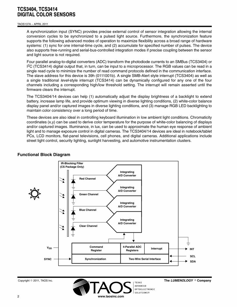
A synchronization input (SYNC) provides precise external control of sensor integration allowing the internalconversion cycles to be synchronized to a pulsed light source. Furthermore, the synchronization featuresupports the following advanced modes of operation to maximize flexibility across a broad range of hardwaresystems: (1) sync for one internal-time cycle, and (2) accumulate for specified number of pulses. The devicealso supports free-running and serial-bus-controlled integration modes if precise coupling between the sensorand light source is not required.
Four parallel analog-to-digital converters (ADC) transform the photodiode currents to an SMBus (TCS3404) orI2C (TCS3414) digital output that, in turn, can be input to a microprocessor. The RGB values can be read in asingle read cycle to minimize the number of read command protocols defined in the communication interface.The slave address for this device is 39h (0111001b). A single SMB-Alert style interrupt (TCS3404) as well asa single traditional level-style interrupt (TCS3414) can be dynamically configured for any one of the fourchannels including a corresponding high/low threshold setting. The interrupt will remain asserted until thefirmware clears the interrupt.
The TCS3404/14 devices can help (1) automatically adjust the display brightness of a backlight to extendbattery, increase lamp life, and provide optimum viewing in diverse lighting conditions, (2) white-color balancedisplay panel and/or captured images in diverse lighting conditions, and (3) manage RGB LED backlighting tomaintain color consistency over a long period of time.
These devices are also ideal in controlling keyboard illumination in low ambient light conditions. Chromaticitycoordinates (x,y) can be used to derive color temperature for the purpose of white-color balancing of displaysand/or captured images. Illuminance, in lux, can be used to approximate the human eye response of ambientlight and to manage exposure control in digital cameras. The TCS3404/14 devices are ideal in notebook/tabletPCs, LCD monitors, flat-panel televisions, cell phones, and digital cameras. Additional applications includestreet light control, security lighting, sunlight harvesting, and automotive instrumentation clusters.
Functional Block Diagram
Two-Wire Serial Interface
Interrupt
SDA
VDD
Blue Channel
Clear Channel
CommandRegister
4-Parallel ADCRegisters INT
SCL
Green Channel
Red Channel
IntegratingA/D Converter
IntegratingA/D Converter
IntegratingA/D Converter
IntegratingA/D Converter
SynchronizationSYNC
IR-Blocking Filter(CS Package Only)
TCS3404, TCS3414DIGITAL COLOR SENSORS
TAOS137A − APRIL 2011
3
The LUMENOLOGY � Company�
�
Copyright � 2011, TAOS Inc.
www.taosinc.com
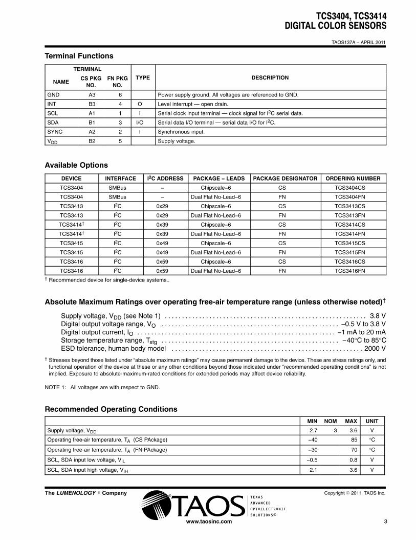
Terminal Functions
TERMINAL
NAMECS PKG
NO.FN PKG
NO.TYPE DESCRIPTION
GND A3 6 Power supply ground. All voltages are referenced to GND.
INT B3 4 O Level interrupt — open drain.
SCL A1 1 I Serial clock input terminal — clock signal for I2C serial data.
SDA B1 3 I/O Serial data I/O terminal — serial data I/O for I2C.
SYNC A2 2 I Synchronous input.
VDD B2 5 Supply voltage.
Available Options
DEVICE INTERFACE I2C ADDRESS PACKAGE − LEADS PACKAGE DESIGNATOR ORDERING NUMBER
TCS3404 SMBus − Chipscale−6 CS TCS3404CS
TCS3404 SMBus − Dual Flat No-Lead−6 FN TCS3404FN
TCS3413 I2C 0x29 Chipscale−6 CS TCS3413CS
TCS3413 I2C 0x29 Dual Flat No-Lead−6 FN TCS3413FN
TCS3414† I2C 0x39 Chipscale−6 CS TCS3414CS
TCS3414† I2C 0x39 Dual Flat No-Lead−6 FN TCS3414FN
TCS3415 I2C 0x49 Chipscale−6 CS TCS3415CS
TCS3415 I2C 0x49 Dual Flat No-Lead−6 FN TCS3415FN
TCS3416 I2C 0x59 Chipscale−6 CS TCS3416CS
TCS3416 I2C 0x59 Dual Flat No-Lead−6 FN TCS3416FN† Recommended device for single-device systems..
Absolute Maximum Ratings over operating free-air temperature range (unless otherwise noted)†
Supply voltage, VDD (see Note 1) 3.8 V. . . . . . . . . . . . . . . . . . . . . . . . . . . . . . . . . . . . . . . . . . . . . . . . . . . . . . . . . . . Digital output voltage range, VO −0.5 V to 3.8 V. . . . . . . . . . . . . . . . . . . . . . . . . . . . . . . . . . . . . . . . . . . . . . . . . . . . Digital output current, IO −1 mA to 20 mA. . . . . . . . . . . . . . . . . . . . . . . . . . . . . . . . . . . . . . . . . . . . . . . . . . . . . . . . . . Storage temperature range, Tstg −40°C to 85°C. . . . . . . . . . . . . . . . . . . . . . . . . . . . . . . . . . . . . . . . . . . . . . . . . . . . ESD tolerance, human body model 2000 V. . . . . . . . . . . . . . . . . . . . . . . . . . . . . . . . . . . . . . . . . . . . . . . . . . . . . . . .
† Stresses beyond those listed under “absolute maximum ratings” may cause permanent damage to the device. These are stress ratings only, andfunctional operation of the device at these or any other conditions beyond those indicated under “recommended operating conditions” is notimplied. Exposure to absolute-maximum-rated conditions for extended periods may affect device reliability.
NOTE 1: All voltages are with respect to GND.
Recommended Operating Conditions
MIN NOM MAX UNIT
Supply voltage, VDD 2.7 3 3.6 V
Operating free-air temperature, TA (CS PAckage) −40 85 °C
Operating free-air temperature, TA (FN PAckage) −30 70 °C
SCL, SDA input low voltage, VIL −0.5 0.8 V
SCL, SDA input high voltage, VIH 2.1 3.6 V
TCS3404, TCS3414DIGITAL COLOR SENSORS
TAOS137A − APRIL 2011
4
�
�
Copyright � 2011, TAOS Inc. The LUMENOLOGY � Company
www.taosinc.com
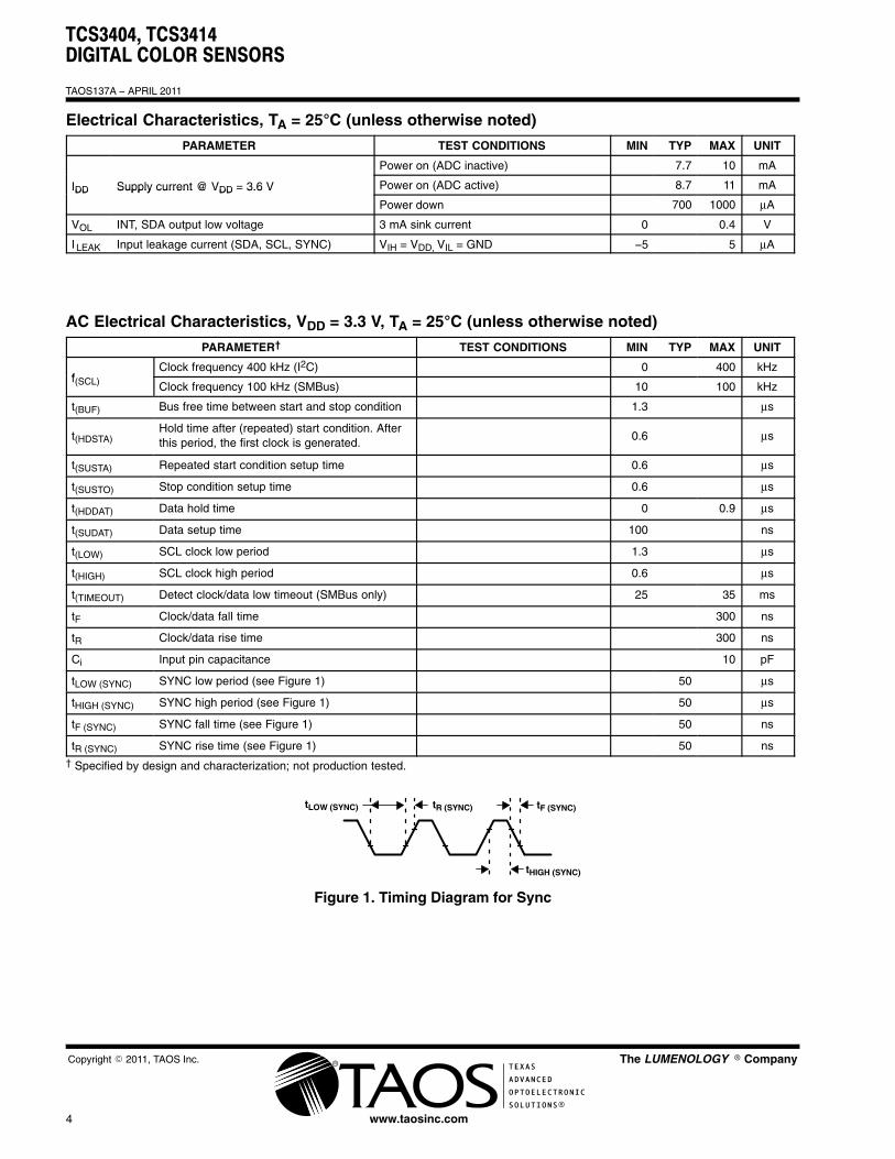
Electrical Characteristics, TA = 25�C (unless otherwise noted)
PARAMETER TEST CONDITIONS MIN TYP MAX UNIT
Power on (ADC inactive) 7.7 10 mA
IDD Supply current @ VDD = 3.6 V Power on (ADC active) 8.7 11 mAIDD Supply current @ VDD 3.6 V
Power down 700 1000 μA
VOL INT, SDA output low voltage 3 mA sink current 0 0.4 V
I LEAK Input leakage current (SDA, SCL, SYNC) VIH = VDD, VIL = GND −5 5 μA
AC Electrical Characteristics, VDD = 3.3 V, TA = 25�C (unless otherwise noted)
PARAMETER† TEST CONDITIONS MIN TYP MAX UNIT
fClock frequency 400 kHz (I2C) 0 400 kHz
f(SCL) Clock frequency 100 kHz (SMBus) 10 100 kHz
t(BUF) Bus free time between start and stop condition 1.3 μs
t(HDSTA)Hold time after (repeated) start condition. Afterthis period, the first clock is generated.
0.6 μs
t(SUSTA) Repeated start condition setup time 0.6 μs
t(SUSTO) Stop condition setup time 0.6 μs
t(HDDAT) Data hold time 0 0.9 μs
t(SUDAT) Data setup time 100 ns
t(LOW) SCL clock low period 1.3 μs
t(HIGH) SCL clock high period 0.6 μs
t(TIMEOUT) Detect clock/data low timeout (SMBus only) 25 35 ms
tF Clock/data fall time 300 ns
tR Clock/data rise time 300 ns
Ci Input pin capacitance 10 pF
tLOW (SYNC) SYNC low period (see Figure 1) 50 μs
tHIGH (SYNC) SYNC high period (see Figure 1) 50 μs
tF (SYNC) SYNC fall time (see Figure 1) 50 ns
tR (SYNC) SYNC rise time (see Figure 1) 50 ns† Specified by design and characterization; not production tested.
tHIGH (SYNC)
tF (SYNC)tR (SYNC)tLOW (SYNC)
Figure 1. Timing Diagram for Sync

TCS3404, TCS3414DIGITAL COLOR SENSORS
TAOS137A − APRIL 2011
5
The LUMENOLOGY � Company�
�
Copyright � 2011, TAOS Inc.
www.taosinc.com
Optical Characteristics, VDD = 3 V, TA = 25�C, GAIN = 64�, Tint = 12ms (unless otherwise noted) (seeNotes 1 and 2)
PARAMETERTEST Red Channel Green Channel Blue Channel Clear Channel
UNITPARAMETERTEST
CONDITIONS MIN TYP MAX MIN TYP MAX MIN TYP MAX MIN TYP MAXUNIT
Irradianceλp = 470 nm,See Note 3
0% 15% 15% 50% 65% 90% 59.0 65.6 72.5
Re
responsivity(CSpackage)
λp = 524 nm,See Note 4
0% 15% 60% 90% 0% 35% 71.2 76.9 82.7(counts/
μW/cm2)package)
λp = 640 nm,See Note 5
80% 110% 0% 15% 0% 15% 80.6 90.1 99.5
cm2)
Irradianceλp = 470 nm,See Note 3
0% 15% 10% 50% 65% 90% 56.3 62.5 69.1
Re
responsivity(FNpackage)
λp = 524 nm,See Note 4
0% 15% 60% 90% 0% 35% 72.5 78.4 84.3(counts/
μW/cm2)package)
λp = 640 nm,See Note 5
80% 110% 0% 15% 0% 15% 94.2 105.3 116.3
cm2)
NOTES: 1. The percentage shown represents the ratio of the respective red, green, or blue channel value to the clear channel value.2. Optical measurements are made using small-angle incident radiation from a light-emitting diode (LED) optical source.3. The 470 nm input irradiance is supplied by an InGaN light-emitting diode with the following characteristics:
peak wavelength λp = 470 nm, spectral halfwidth Δλ½ = 35 nm, and luminous efficacy = 75 lm/W.4. The 524 nm input irradiance is supplied by an InGaN light-emitting diode with the following characteristics:
peak wavelength λp = 524 nm, spectral halfwidth Δλ½ = 47 nm, and luminous efficacy = 520 lm/W.5. The 640 nm input irradiance is supplied by a AlInGaP light-emitting diode with the following characteristics:
peak wavelength λp = 640 nm, spectral halfwidth Δλ½ = 17 nm, and luminous efficacy = 155 lm/W.6. Illuminance responsivity Rv is calculated from the irradiance responsivity Re by using the LED luminous efficacy values stated in
notes 3, 4, and 5 and using 1 lx = 1 lm/m2.
Operating Characteristics, VDD = 3 V, TA = 25�C, (unless otherwise noted) (see Notes 2, 3, and 4)
PARAMETER TEST CONDITIONS MIN TYP MAX UNIT
4× 3.8 4 4.2
Gain scaling, relative to 1× gain setting 16× 15.2 16 16.8Gain scaling, relative to 1× gain setting
64× 60.8 64 67.2
Dark ADC count value Ee = 0, 64× gain setting, Tint = 400 ms 0 3 15 counts
Maximum digital count value Prescale = 1, Tint = 400 ms (Note 1) 65535 counts
fosc Oscillator frequency 4.2 4.4 4.6 MHz
Internal integration time tolerance −5 5 %
Temperature coefficient of responsivity (SYNC mode) λ � 700 nm, −40°C � TA � 85°C ± 200 ppm/°C
NOTES: 1. At shorter integration times and/or higher Prescale settings, the device will reach saturation of the analog section before the digitalcount reaches the maximum 16-bit value. The worst-case (lowest) analog saturation value can be obtained using the formula: Analogsaturation = (fosc(min) ×Tint) ÷Prescale, where Fosc(min) is the minimum oscillator frequency in Hz, and tint is the actual integrationtime (internal, manually-timed, or sync-generated) in seconds.
2. Gain is controlled by the gain register (07h) described in the Register section.3. Measurements taken when the Photodiode field value in the Photodiode Register (06h) is 00b and when the Prescaler field value
in the Gain Register (07h) is 000b.4. The full scale ADC count value is slew-rate limited for short integration times and is limited by the 16-bit counter for long integration
times. The nominal transition between the two regions is tint = 65535/5000 = 13.1 ms.
TCS3404, TCS3414DIGITAL COLOR SENSORS
TAOS137A − APRIL 2011
6
�
�
Copyright � 2011, TAOS Inc. The LUMENOLOGY � Company
www.taosinc.com
PARAMETER MEASUREMENT INFORMATION
SDA
SCL
StopStart
SCLACKt(LOWMEXT) t(LOWMEXT)
t(LOWSEXT)
SCLACK
t(LOWMEXT)
StartCondition
StopCondition
P
SDA
t(SUSTO)t(SUDAT)t(HDDAT)t(BUF)
VIH
VIL
SCL
t(SUSTA)t(HIGH)
t(F)t(R)
t(HDSTA)
t(LOW)
VIH
VIL
P SS
Figure 2. Timing Diagrams
A0A1A2A3A4A5A6
SCL
Start byMaster
SDA
1 9 1 9
D1D2D3D4D5D6D7 D0R/W
Frame 1 Slave Address Byte Frame 2 Command Byte
ACK byTCS3404/14
Stop byMaster
ACK byTCS3404/14
Figure 3. Example Timing Diagram for Send Byte Format
A0A1A2A3A4A5A6
SCL
Start byMaster
SDA
1 9 1 9
D1D2D3D4D5D6D7 D0R/W
Frame 1 Slave Address Byte Frame 2 Data Byte From TCS3404/14
ACK byTCS3404/14
Stop byMaster
NACK byMaster
Figure 4. Example Timing Diagram for Receive Byte Format

TCS3404, TCS3414DIGITAL COLOR SENSORS
TAOS137A − APRIL 2011
7
The LUMENOLOGY � Company�
�
Copyright � 2011, TAOS Inc.
www.taosinc.com
TYPICAL CHARACTERISTICS
Figure 5
SPECTRAL RESPONSIVITYCS PACKAGE
λ − Wavelength − nm
0400
20
40
60
80
100
500 600 700 800 900 1000 1100
No
rmal
ized
Res
po
nsi
vity
— %
300
Clear
Blue
Green
Red
Figure 6
SPECTRAL RESPONSIVITYFN PACKAGE
λ − Wavelength − nm
0400
20
40
60
80
100
500 600 700 800 900 1000 1100N
orm
aliz
ed R
esp
on
sivi
ty —
%300
120
Clear
Red
Green
Blue
Note: Spectral responsivity is normalized at 655 nm. Note: Spectral responsivity is normalized at 850 nm.
Figure 7
IDD OFFvs.
FREE-AIR TEMPERATURE(Power Down)
TA − Free-Air Temperature − °C
I DD
— �
A
600
650
700
750
800
850
900
950
0 25 50 75 100
3.6 V
2.7 V
3.0 V
3.3 V
Figure 8
I DD
— m
A
0 25 50 75 100
IDD ONvs.
FREE-AIR TEMPERATURE(Power On — ADC Inactive)
TA − Free-Air Temperature − °C
2.7 V
3.0 V
7.0
7.5
8.0
8.5
9.0
9.5
3.6 V
3.3 V
Note: When the device is powered on and the ADC is active, IDD is approximately 1 mA higher.
TCS3404, TCS3414DIGITAL COLOR SENSORS
TAOS137A − APRIL 2011
8
�
�
Copyright � 2011, TAOS Inc. The LUMENOLOGY � Company
www.taosinc.com
TYPICAL CHARACTERISTICS
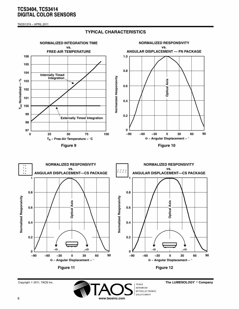
Figure 9
98
99
100
101
102
103
104
105
106
97
Tin
t No
rmal
ized
— %
0 25 50 75 100
NORMALIZED INTEGRATION TIMEvs.
FREE-AIR TEMPERATURE
TA − Free-Air Temperature − °C
Externally Timed Integration
Internally TimedIntegration
Figure 10
NORMALIZED RESPONSIVITYvs.
ANGULAR DISPLACEMENT — FN PACKAGE
� − Angular Displacement − °
No
rmal
ized
Res
po
nsi
vity
0
0.2
0.4
0.6
0.8
1.0
−90 −60 −30 0 30 60 90
Op
tica
l Axi
s
Figure 11
NORMALIZED RESPONSIVITYvs.
ANGULAR DISPLACEMENT—CS PACKAGE
� − Angular Displacement − °
No
rmal
ized
Res
po
nsi
vity
0
0.2
0.4
0.6
0.8
1
−90 −60 −30 0 30 60 90
Op
tica
l Axi
s
�� ��
Figure 12
NORMALIZED RESPONSIVITYvs.
ANGULAR DISPLACEMENT—CS PACKAGE
� − Angular Displacement − °
No
rmal
ized
Res
po
nsi
vity
0
0.2
0.4
0.6
0.8
1
−90 −60 −30 0 30 60 90
Op
tica
l Axi
s
�� ��

TCS3404, TCS3414DIGITAL COLOR SENSORS
TAOS137A − APRIL 2011
9
The LUMENOLOGY � Company�
�
Copyright � 2011, TAOS Inc.
www.taosinc.com
PRINCIPLES OF OPERATION
Analog-to-Digital Converter
The TCS3404/14 contains four integrating analog-to-digital converters (ADC) that integrate the currents fromthe four photodiodes (channel 1 through channel 4). Integration of all four channels occurs simultaneously, andupon completion of the conversion cycle the conversion results are transferred to the channel data registers,respectively. The transfers are double-buffered to ensure that invalid data is not read during the transfer. Afterthe transfer, the device automatically begins the next integration cycle.
There are two ways to control the integration cycles: internally timed and externally timed. Internally-timedintegration cycles can either be continuous back-to-back conversions or can be externally triggered as a singleevent using the SYNC pin. Externally-timed integrations can be controlled by setting and clearing a register bit(i.e. ADC_EN in Control Register) using the serial interface, or by 1 or more pulses input to the SYNC pin.Integration options are configured through the Timing Register (see the Timing Register section for moreinformation).
Digital Interface
Interface and control of the TCS3404/14 is accomplished through a two-wire serial interface to a set of registersthat provide access to device control functions and output data. The serial interface is compatible with SystemManagement Bus (SMBus) versions 1.1 and 2.0, and I2C bus Fast-Mode.
The TCS3404/14 device supports a single slave address outlined in Table 1. Additional devices shown in theAvailable Options table on page 3 support additional I2C slave addresses for systems requiring more than onedevice.
Table 1. Slave Address
SLAVE ADDRESS SMB ALERT ADDRESS
0111001 0001100
NOTE: The slave and SMB Alert addresses are 7 bits. Please note the SMBus and I2C protocols on the following pages. A read/write bit shouldbe appended to the slave address by the master device to communicate properly with the device.
Interrupt
Although the ADC channel data registers can be read at any time to obtain the most recent conversion value,in some applications, periodic polling of the device may not be desirable. For these types of applications, thedevice supports a variety of interrupt options allowing the user to configure the device to signal when a changein light intensity has occurred. High and low threshold registers allow a range of light levels to be defined, outsideof which the device generates an interrupt. A persistence setting allows the user to specify a time duration thatthe measured value must remain outside of the defined range before generating an interrupt. The interruptfunction can be assigned to any one of the four ADC color channels. See Interrupt Control Register for moreinformation on configuring the interrupt functions.

TCS3404, TCS3414DIGITAL COLOR SENSORS
TAOS137A − APRIL 2011
10
�
�
Copyright � 2011, TAOS Inc. The LUMENOLOGY � Company
www.taosinc.com
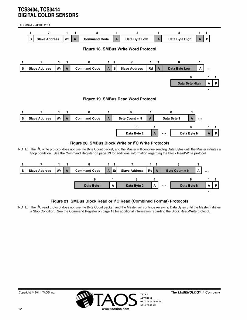
SMBus and I2C Protocols
Each Send and Write protocol is, essentially, a series of bytes. A byte sent to the TCS3404/14 with the mostsignificant bit (MSB) equal to 1 will be interpreted as a COMMAND byte. The lower four bits of the COMMANDbyte form the register select address (see Table 1), which is used to select the destination for the subsequentbyte(s) received. The TCS3404/14 responds to any Receive Byte requests with the contents of the registerspecified by the stored register select address.
The TCS3404/14 implements the following protocols of the SMB 2.0 specification:
� Send Byte Protocol
� Receive Byte Protocol
� Write Byte Protocol
� Write Word Protocol
� Read Word Protocol
� Block Write Protocol
� Block Read Protocol
The TCS3404/14 implements the following protocols of the I2C specification:
� I2C Write Protocol
� I2C Read (Combined Format) Protocol
When an SMBus Block Write or Block Read is initiated (see description of COMMAND Register), the bytefollowing the COMMAND byte is ignored but is a requirement of the SMBus specification. This field containsthe byte count (i.e. the number of bytes to be transferred). The TCS3404 (SMBus) device ignores this field andextracts this information by counting the actual number of bytes transferred before the Stop condition isdetected.
When an I2C Write or I2C Read (Combined Format) is initiated, the byte count is also ignored but follows theSMBus protocol specification. Data bytes continue to be transferred from the TCS3414 (I2C) device to Masteruntil a NACK is sent by the Master.
The data formats supported by the TCS3404 and TCS3414 devices are:
� Master transmitter transmits to slave receiver (SMBus and I2C):
− The transfer direction in this case is not changed.
� Master reads slave immediately after the first byte (SMBus only):
− At the moment of the first acknowledgment (provided by the slave receiver) the master transmitterbecomes a master receiver and the slave receiver becomes a slave transmitter.
� Combined format (SMBus and I2C):
− During a change of direction within a transfer, the master repeats both a START condition and the slaveaddress but with the R/W bit reversed. In this case, the master receiver terminates the transfer bygenerating a NACK on the last byte of the transfer and a STOP condition.
For a complete description of SMBus protocols, please review the SMBus Specification athttp://www.smbus.org/specs. For a complete description of the I2C protocol, please review the NXP I2C designspecification at http://www.i2c−bus.org/references/.

TCS3404, TCS3414DIGITAL COLOR SENSORS
TAOS137A − APRIL 2011
11
The LUMENOLOGY � Company�
�
Copyright � 2011, TAOS Inc.
www.taosinc.com
Wr
7
Data ByteSlave AddressS
1
A PA
81 1 1 1
X X
A Acknowledge (this bit position may be 0 for an ACK or 1 for a NACK)
P Stop Condition
Rd Read (bit value of 1)
S Start Condition
Sr Repeated Start Condition
Wr Write (bit value of 0)
X Shown under a field indicates that that field is required to have a value of X
... Continuation of protocol
Master-to-Slave
Slave-to-Master
Figure 13. SMBus and I2C Packet Protocol Element Key
Wr
7
Data ByteSlave AddressS
1
A PA
81 1 1 1
Figure 14. SMBus Send Byte Protocol
Rd
7
Data ByteSlave AddressS
1
A PA
81 1 1 1
1
Figure 15. SMBus Receive Byte Protocol
Wr
7
Data ByteSlave AddressS
1
A AA
81 1 1 8
Command Code
1
P
1
Figure 16. SMBus Write Byte Protocol
Wr
7
Data Byte LowSlave AddressS
1
A A
81 1 1
Command Code
1
P
81 1
RdSlave AddressS A A
7 1 1
1
Figure 17. SMBus Read Byte Protocol
TCS3404, TCS3414DIGITAL COLOR SENSORS
TAOS137A − APRIL 2011
12
�
�
Copyright � 2011, TAOS Inc. The LUMENOLOGY � Company
www.taosinc.com
Wr
7
Data Byte LowSlave AddressS
1
A AA
81 1 1 8
Command Code
1
PData Byte High A
8 1 1
Figure 18. SMBus Write Word Protocol
Wr
7
Data Byte LowSlave AddressS
1
A A
81 1 1
Command Code
1
PData Byte High A
81 1
RdSlave AddressS A A ...7 1
8 1 1
1
Figure 19. SMBus Read Word Protocol
Wr
8
Data Byte 1Slave AddressS
1
A A
81 1 1
Command Code
PData Byte N A
81 1
Byte Count = N A A ...7
8 1 1
Data Byte 2 A
8 1
...
Figure 20. SMBus Block Write or I2C Write ProtocolsNOTE: The I2C write protocol does not use the Byte Count packet, and the Master will continue sending Data Bytes until the Master initiates a
Stop condition. See the Command Register on page 13 for additional information regarding the Block Read/Write protocol.
Wr
7
Byte Count = NSlave AddressS
1
A A
81 1 1
Command Code
PData Byte N A
81 1
Slave Address A A ...7
8 1 1
Data Byte 2 A
8 1
...Data Byte 1 A
8 1
1
Sr
1
Rd
1
Figure 21. SMBus Block Read or I2C Read (Combined Format) ProtocolsNOTE: The I2C read protocol does not use the Byte Count packet, and the Master will continue receiving Data Bytes until the Master initiates
a Stop Condition. See the Command Register on page 13 for additional information regarding the Block Read/Write protocol.

TCS3404, TCS3414DIGITAL COLOR SENSORS
TAOS137A − APRIL 2011
13
The LUMENOLOGY � Company�
�
Copyright � 2011, TAOS Inc.
www.taosinc.com
Register Set
The TCS3404/14 is controlled and monitored by 18 user registers and a command register accessed throughthe serial interface. These registers provide for a variety of control functions and can be read to determine resultsof the ADC conversions. The register set is summarized in Table 2.
Table 2. Register Set
ADDRESS REGISTER NAME REGISTER FUNCTION
−− COMMAND Specifies register address
00h CONTROL Control of basic functions
01h TIMING Integration time/gain control
02h INTERRUPT Interrupt control
03h INT SOURCE Interrupt source
04h ID Part number/ Rev ID
07h GAIN ADC gain control
08h LOW_THRESH_LOW_BYTE Low byte of low interrupt threshold
09h LOW_THRESH_HIGH_BYTE High byte of low interrupt threshold
0Ah HIGH_THRESH_LOW_BYTE Low byte of high interrupt threshold
0Bh HIGH_THRESH_HIGH_BYTE High byte of high interrupt threshold
0Fh −− SMBus block read (10h through 17h)
10h DATA1LOW Low byte of ADC green channel
11h DATA1HIGH High byte of ADC green channel
12h DATA2LOW Low byte of ADC red channel
13h DATA2HIGH High byte of ADC red channel
14h DATA3LOW Low byte of ADC blue channel
15h DATA3HIGH High byte of ADC blue channel
16h DATA4LOW Low byte of ADC clear channel
17h DATA4HIGH High byte of ADC clear channel
The mechanics of accessing a specific register depends on the specific SMB protocol used. Refer to the sectionon SMBus protocols on the previous pages. In general, the COMMAND register is written first to specify thespecific control/status register for following read/write operations.

TCS3404, TCS3414DIGITAL COLOR SENSORS
TAOS137A − APRIL 2011
14
�
�
Copyright � 2011, TAOS Inc. The LUMENOLOGY � Company
www.taosinc.com
Command Register
The command register specifies the address of the target register for subsequent read and write operations.This register contains eight bits as described in Table 3 and defaults to 00h at power on.
Table 3. Command Register
67 5 4
ADDRESS
23 1 0
00 0 0 00 0 0Reset Value:
COMMANDCMD TRANSACTION
FIELD BITS DESCRIPTION
CMD 7 Select command register. Must write as 1.
Transaction. Selects type of transaction to follow in subsequent data transfer.
FIELD VALUE TRANSACTION DESCRIPTION
00 Byte protocol SMB read/write byte protocolTRANSACTION 6:5 01 Word protocol SMB read/write word protocol
10 Block protocol SMB read/write block protocol
11 Interrupt clear Clear any pending interrupt and is a write-once-to-clear field
ADDRESS 4:0 Register Address. This field selects the specific control or status register for following write and read com-mands according to Table 2.
NOTES: 1. An I2C block transaction will continue until the Master sends a stop condition. See Figure 18 and Figure 19. Unlike the I2C protocol,the TCS3404/14 SMBus read/write protocol requires a Byte Count. All eight ADC Channel Data Registers (10h through 17h) canbe read simultaneously in a single SMBus transaction. This is the only 64-bit data block supported by the TCS3404 SMBus protocol.The TRANSACTION field must be set to 10, and a read condition should be initiated with a COMMAND CODE of CFh. By usinga COMMAND CODE of CFh during an SMBus Block Read Protocol, the TCS3404 device will automatically insert the appropriateByte Count (Byte Count = 8) as illustrated in Figure 18. A write condition should not be used in conjunction with the 0Fh register.
2. Only the Send Byte Protocol should be used when clearing interrupts.
TCS3404, TCS3414DIGITAL COLOR SENSORS
TAOS137A − APRIL 2011
15
The LUMENOLOGY � Company�
�
Copyright � 2011, TAOS Inc.
www.taosinc.com
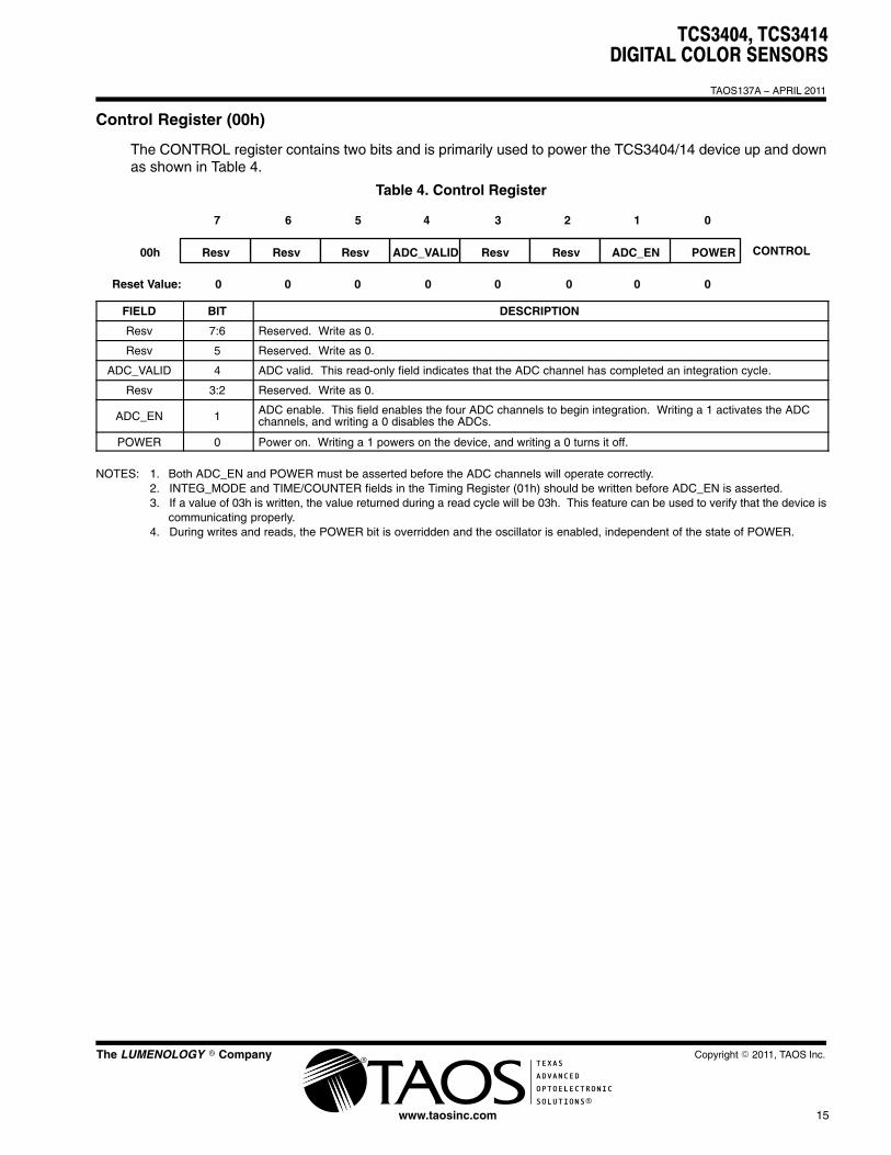
Control Register (00h)
The CONTROL register contains two bits and is primarily used to power the TCS3404/14 device up and downas shown in Table 4.
Table 4. Control Register
67 5 4
POWER
23 1 0
00 0 0 00 0 0Reset Value:
CONTROLResvResv Resv ADC_VALID Resv00h Resv ADC_EN
FIELD BIT DESCRIPTION
Resv 7:6 Reserved. Write as 0.
Resv 5 Reserved. Write as 0.
ADC_VALID 4 ADC valid. This read-only field indicates that the ADC channel has completed an integration cycle.
Resv 3:2 Reserved. Write as 0.
ADC_EN 1 ADC enable. This field enables the four ADC channels to begin integration. Writing a 1 activates the ADCchannels, and writing a 0 disables the ADCs.
POWER 0 Power on. Writing a 1 powers on the device, and writing a 0 turns it off.
NOTES: 1. Both ADC_EN and POWER must be asserted before the ADC channels will operate correctly.2. INTEG_MODE and TIME/COUNTER fields in the Timing Register (01h) should be written before ADC_EN is asserted.3. If a value of 03h is written, the value returned during a read cycle will be 03h. This feature can be used to verify that the device is
communicating properly.4. During writes and reads, the POWER bit is overridden and the oscillator is enabled, independent of the state of POWER.

TCS3404, TCS3414DIGITAL COLOR SENSORS
TAOS137A − APRIL 2011
16
�
�
Copyright � 2011, TAOS Inc. The LUMENOLOGY � Company
www.taosinc.com
Timing Register (01h)
The TIMING register controls the synchronization and integration time of the ADC channels. The TimingRegister settings apply to all four ADC channels. The Timing Register defaults to 00h at power on.
Table 5. Timing Register
67 5 4
PARAM
23 1 0
00 0 0 00 0 0Reset Value:
TIMINGSYNC_EDGEResv INTEG_MODE01h
FIELD BITS DESCRIPTION
Resv 7 Reserved. Write as 0.
SYNC_EDGE 6Sync pin edge. If SYNC_EDGE is low, the falling edge of the sync pin is used to stop an integrationcycle when INTEG_MODE is 11. If SYNC_EDGE is high, the rising edge of the sync pin is used tostop an integration cycle when INTEG_MODE is 11.
Selects preset integration time, manual integration (via serial bus), or external synchronization (SYNCIN) modes.
FIELD VALUE MODE
00In this mode, the integrator is free-running and one of the threeinternally-generated Nominal Integration Times is selected for each conversion(see Integration Time table below).
INTEG_MODE 5:4 01 Manually start/stop integration through serial bus using ADC_EN field in Con-trol Register.
10Synchronize exactly one internally-timed integration cycle as specified in theNOMINAL INTEGRATION TIME beginning 2.4 μs after being initiated by theSYNC IN pin.
11Integrate over specified number of pulses on SYNC IN pin (See SYNC INPULSE COUNT table below). Minimum width of sync pulse is 50 μs. SYNCIN must be low at least 3.6 μs.
Uses single, multipurpose bitmapped field to select one of three predefined integration times or set thenumber of SYNC IN pulses to count when the INTEG_MODE accumulate mode (11) is selected.
NOTE: INTEG_MODE and TIME/COUNTER fields should be written before ADC_EN is asserted.
FIELD VALUE NOMINAL INTEGRATION TIME
0000 12 ms
0001 100 ms
0010 400 ms
PARAM 3:0FIELD VALUE SYNC IN PULSE COUNT
PARAM 3:00000 1
0001 2
0010 4
0011 8
0100 16
0101 32
0110 64
0111 128
1000 256
TCS3404, TCS3414DIGITAL COLOR SENSORS
TAOS137A − APRIL 2011
17
The LUMENOLOGY � Company�
�
Copyright � 2011, TAOS Inc.
www.taosinc.com
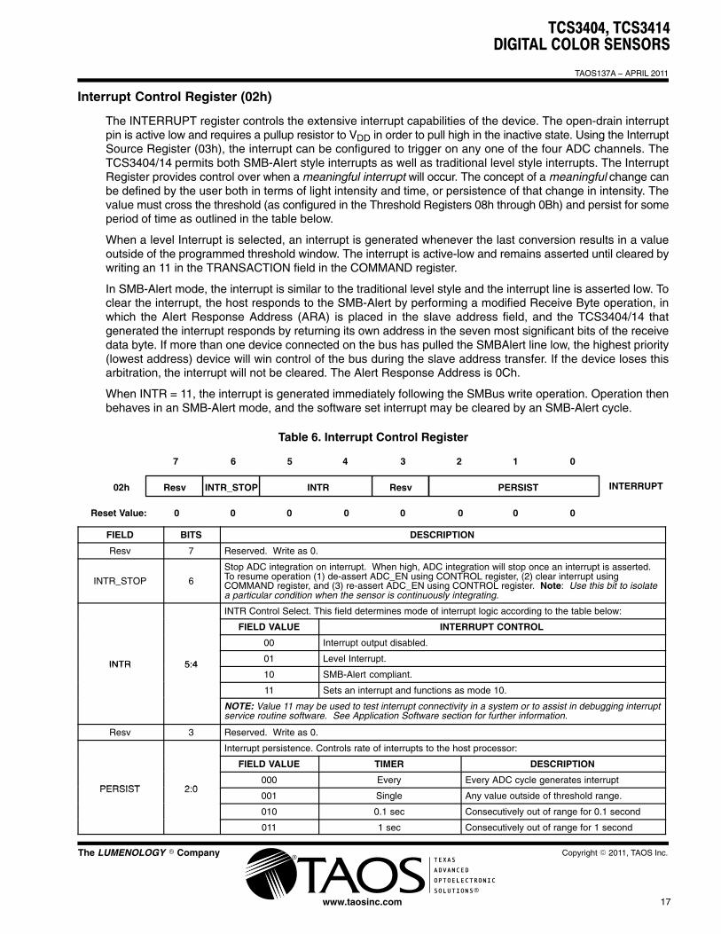
Interrupt Control Register (02h)
The INTERRUPT register controls the extensive interrupt capabilities of the device. The open-drain interruptpin is active low and requires a pullup resistor to VDD in order to pull high in the inactive state. Using the InterruptSource Register (03h), the interrupt can be configured to trigger on any one of the four ADC channels. TheTCS3404/14 permits both SMB-Alert style interrupts as well as traditional level style interrupts. The InterruptRegister provides control over when a meaningful interrupt will occur. The concept of a meaningful change canbe defined by the user both in terms of light intensity and time, or persistence of that change in intensity. Thevalue must cross the threshold (as configured in the Threshold Registers 08h through 0Bh) and persist for someperiod of time as outlined in the table below.
When a level Interrupt is selected, an interrupt is generated whenever the last conversion results in a valueoutside of the programmed threshold window. The interrupt is active-low and remains asserted until cleared bywriting an 11 in the TRANSACTION field in the COMMAND register.
In SMB-Alert mode, the interrupt is similar to the traditional level style and the interrupt line is asserted low. Toclear the interrupt, the host responds to the SMB-Alert by performing a modified Receive Byte operation, inwhich the Alert Response Address (ARA) is placed in the slave address field, and the TCS3404/14 thatgenerated the interrupt responds by returning its own address in the seven most significant bits of the receivedata byte. If more than one device connected on the bus has pulled the SMBAlert line low, the highest priority(lowest address) device will win control of the bus during the slave address transfer. If the device loses thisarbitration, the interrupt will not be cleared. The Alert Response Address is 0Ch.
When INTR = 11, the interrupt is generated immediately following the SMBus write operation. Operation thenbehaves in an SMB-Alert mode, and the software set interrupt may be cleared by an SMB-Alert cycle.
Table 6. Interrupt Control Register
67 5 4 23 1 0
00 0 0 00 0 0Reset Value:
INTERRUPTINTR_STOPResv INTR Resv02h PERSIST
FIELD BITS DESCRIPTION
Resv 7 Reserved. Write as 0.
INTR_STOP 6
Stop ADC integration on interrupt. When high, ADC integration will stop once an interrupt is asserted.To resume operation (1) de-assert ADC_EN using CONTROL register, (2) clear interrupt usingCOMMAND register, and (3) re-assert ADC_EN using CONTROL register. Note: Use this bit to isolatea particular condition when the sensor is continuously integrating.
INTR Control Select. This field determines mode of interrupt logic according to the table below:
FIELD VALUE INTERRUPT CONTROL
00 Interrupt output disabled.
INTR 5:401 Level Interrupt.
INTR 5:410 SMB-Alert compliant.
11 Sets an interrupt and functions as mode 10.
NOTE: Value 11 may be used to test interrupt connectivity in a system or to assist in debugging interruptservice routine software. See Application Software section for further information.
Resv 3 Reserved. Write as 0.
Interrupt persistence. Controls rate of interrupts to the host processor:
FIELD VALUE TIMER DESCRIPTION
PERSIST 2:0000 Every Every ADC cycle generates interrupt
PERSIST 2:0001 Single Any value outside of threshold range.
010 0.1 sec Consecutively out of range for 0.1 second
011 1 sec Consecutively out of range for 1 second

TCS3404, TCS3414DIGITAL COLOR SENSORS
TAOS137A − APRIL 2011
18
�
�
Copyright � 2011, TAOS Inc. The LUMENOLOGY � Company
www.taosinc.com
Interrupt Source Register (03h)
The Interrupt Source register selects which ADC channel value to use to generate an interrupt. Only one of thefour ADC channels can be selected.
Table 7. Interrupt Source Register
67 5 4
INT SOURCE
23 1 0
00 0 0 00 0 0Reset Value:
INT SOURCEResvResv Resv Resv Resv03h Resv
FIELD BITS DESCRIPTION
Resv 7:2 Reserved. Write as 0.
Interrupt Source. Selects which ADC channel to use to generate an interrupt:
FIELD VALUE INTERRUPT SOURCE
INT SOURCE 1:000 Green channel
INT SOURCE 1:001 Red channel
10 Blue channel
11 Clear channel
NOTE: The INTERRUPT THRESHOLD Register (08h−0Bh) should be configured appropriately to correspond to the ADC channel value thatgenerates an interrupt.
ID Register (04h)
The ID register provides the value for both the part number and silicon revision number for that part number.It is a read-only register, whose value never changes.
Table 8. ID Register
67 5 4
REVNO
23 1 0
−− − − −− − −Reset Value:
IDPARTNO04h
FIELD BITS DESCRIPTION
PARTNO 7:4 Part Number Identification: field value 0000 = TCS3404 field value 0001 = TCS3413, TCS3414, TCS3415, and TCS3416
REVNO 3:0 Revision number identification
TCS3404, TCS3414DIGITAL COLOR SENSORS
TAOS137A − APRIL 2011
19
The LUMENOLOGY � Company�
�
Copyright � 2011, TAOS Inc.
www.taosinc.com
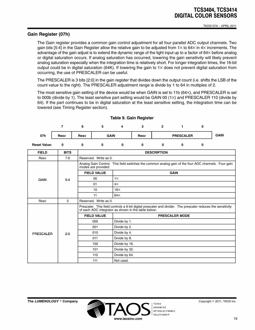
Gain Register (07h)
The Gain register provides a common gain control adjustment for all four parallel ADC output channels. Twogain bits [5:4] in the Gain Register allow the relative gain to be adjusted from 1× to 64× in 4× increments. Theadvantage of the gain adjust is to extend the dynamic range of the light input up to a factor of 64× before analogor digital saturation occurs. If analog saturation has occurred, lowering the gain sensitivity will likely preventanalog saturation especially when the integration time is relatively short. For longer integration times, the 16-bitoutput could be in digital saturation (64K). If lowering the gain to 1× does not prevent digital saturation fromoccurring, the use of PRESCALER can be useful.
The PRESCALER is 3 bits [2:0] in the gain register that divides down the output count (i.e. shifts the LSB of thecount value to the right). The PRESCALER adjustment range is divide by 1 to 64 in multiples of 2.
The most sensitive gain setting of the device would be when GAIN is set to 11b (64×), and PRESCALER is setto 000b (divide by 1). The least sensitive part setting would be GAIN 00 (1×) and PRESCALER 110 (divide by64). If the part continues to be in digital saturation at the least sensitive setting, the integration time can belowered (see Timing Register section).
Table 9. Gain Register
67 5 4 23 1 0
00 0 0 00 0 0Reset Value:
GAINResv GAIN Resv07h PRESCALERResv
FIELD BITS DESCRIPTION
Resv 7:6 Reserved. Write as 0.
Analog Gain Control. This field switches the common analog gain of the four ADC channels. Four gainmodes are provided:
FIELD VALUE GAIN
GAIN 5:4 00 1×GAIN 5:401 4×10 16×11 64×
Resv 3 Reserved. Write as 0.
Prescaler. This field controls a 6-bit digital prescaler and divider. The prescaler reduces the sensitivityof each ADC integrator as shown in the table below:
FIELD VALUE PRESCALER MODE
000 Divide by 1.
001 Divide by 2.
PRESCALER 2:0 010 Divide by 4.PRESCALER 2:0011 Divide by 8.
100 Divide by 16.
101 Divide by 32.
110 Divide by 64.
111 Not used.

TCS3404, TCS3414DIGITAL COLOR SENSORS
TAOS137A − APRIL 2011
20
�
�
Copyright � 2011, TAOS Inc. The LUMENOLOGY � Company
www.taosinc.com
Interrupt Threshold Register (08h − 0Bh)
The interrupt threshold registers store the values to be used as the high and low trigger points for the comparisonfunction for interrupt generation. The high and low bytes from each set of registers are combined to form a 16-bitthreshold value. If the value generated by the Interrupt Source Register (03h) converges below or equal to thelow threshold specified, an interrupt is asserted on the interrupt pin. If the value generated by Interrupt SourceRegister (03h) converges above the high threshold specified, an interrupt is asserted on the interrupt pin.Registers LOW_THRESH_LOW_BYTE and LOW_THRESH_HIGH_BYTE provide the low byte and high byte,respectively, of the lower interrupt threshold. Registers HIGH_THRESH_LOW_BYTE andHIGH_THRESH_HIGH_BYTE provide the low and high bytes, respectively, of the upper interrupt threshold.The interrupt threshold registers default to 00h on power up.
Table 10. Interrupt Threshold Register
REGISTER ADDRESS BITS DESCRIPTION
LOW_THRESH_LOW_BYTE 08h 7:0 ADC interrupt source lower byte of the low threshold.
LOW_THRESH_HIGH_BYTE 09h 7:0 ADC interrupt source upper byte of the low threshold.
HIGH_THRESH_LOW_BYTE 0Ah 7:0 ADC interrupt source lower byte of the high threshold.
HIGH_THRESH_HIGH_BYTE 0Bh 7:0 ADC interrupt source upper byte of the high threshold.
NOTES: 1. The Interrupt Source Register (03h) selects which ADC channel to generate an interrupt and should correspond to the thresholdsetting. Both registers should be configured appropriately when setting up an interrupt service routine.
2. Since two 8-bit values are combined for a single 16-bit value for each of the high and low interrupt thresholds, the SMBus Send Byteprotocol should not be used to write to these registers. Any values transferred by the Send Byte protocol with the MSB set wouldbe interpreted as the COMMAND field and stored as an address for subsequent read/write operations and not as the interruptthreshold information as desired. The Write Word protocol should be used to write byte-paired registers. For example, theLOW_THRESH_LOW_BYTE and LOW_THRESH_HIGH_BYTE registers (as well as the HIGH_THRESH_LOW_BYTE andHIGH_THRESH_HIGH_BYTE registers) can be written together to set the 16-bit ADC value in a single transaction.
ADC Channel Data Registers (10h − 17h)
The ADC channel data are expressed as 16-bit values spread across four registers. The channel low and highprovide the lower and upper bytes respectively for each ADC channel data registers. Each DATALOW andDATAHIGH register is identified below as 1, 2, 3, or 4. All channel data registers are read-only and default to00h on power up.
Table 11. ADC Channel Data Registers
REGISTER ADDRESS BITS DESCRIPTION
GREEN_LOW 10h 7:0 ADC channel 1 lower byte
GREEN_HIGH 11h 7:0 ADC channel 1 upper byte
RED_LOW 12h 7:0 ADC channel 2 lower byte
RED_HIGH 13h 7:0 ADC channel 2 upper byte
BLUE_LOW 14h 7:0 ADC channel 3 lower byte
BLUE_HIGH 15h 7:0 ADC channel 3 upper byte
CLEAR_LOW 16h 7:0 ADC channel 4 lower byte
CLEAR_HIGH 17h 7:0 ADC channel 4 upper byte
The upper byte data registers can only be read following a read to the corresponding lower byte register. Whenthe lower byte register is read the upper eight bits are strobed into a shadow register, which is read by asubsequent read to the upper byte. The upper register will therefore read the correct value even if additionalADC integration cycles complete between the reading of the lower and upper registers.
NOTE: The SMBus Read Word protocol can be used to read byte-paired registers. For example, the DATA1LOW and DATA1HIGH registers (aswell as the other three individual register pairs) may be read together to obtain the 16-bit ADC value in a single transaction.

TCS3404, TCS3414DIGITAL COLOR SENSORS
TAOS137A − APRIL 2011
21
The LUMENOLOGY � Company�
�
Copyright � 2011, TAOS Inc.
www.taosinc.com
APPLICATION INFORMATION: SOFTWARE
Basic Operation
After applying VDD, the device will initially be in the power−down state. To operate the device, issue a commandto access the control register followed by the data value 03h to the control register to set ADC_EN and POWERto power up the device. At this point, all four ADC channels will begin a conversion at the default integration timeof 12 ms. After 12 ms, the conversion results will be available in ADC Channel Data Registers (10h through 17h).The following pseudo code illustrates a procedure for reading the TCS3404/14 device using Word and Bytetransactions:
// Read ADC Channels Using Read Word Protocol − RECOMMENDEDAddress = 0x39Command = 0x80PowerUp = 0x03 //Power Up and Enable ADC//Wait for integration conversion
//Address the Ch1 lower data register and configure for Read WordCommand = 0xB0 //Set Command bit and Word transaction
//Reads two bytes from sequential registers 10h and 11h//Results are returned in DataLow and DataHigh variablesReadWord (Address, Command, DataLow, DataHigh)Channel1 = 256 * DataHigh + DataLow
//Address the Ch2 lower data register and configure for Read WordCommand = 0xB2 //Set Command bit and Word transaction
//Reads two bytes from sequential registers 12h and 13h//Results are returned in DataLow and DataHigh variablesReadWord (Address, Command, DataLow, DataHigh)Channel2 = 256 * DataHigh + DataLow //Shift DataHigh to upper byte
//Address the Ch3 lower data register and configure for Read WordCommand = 0xB4 //Set Command bit and Word transaction
//Reads two bytes from sequential registers 14h and 15h//Results are returned in DataLow and DataHigh variablesReadWord (Address, Command, DataLow, DataHigh)Channel3 = 256 * DataHigh + DataLow
//Address the Ch4 lower data register and configure for Read WordCommand = 0xB8 //Set Command bit and Word transaction
//Reads two bytes from sequential registers 16h and 17h//Results are returned in DataLow and DataHigh variablesReadWord (Address, Command, DataLow, DataHigh)Channel4 = 256 * DataHigh + DataLow //Shift DataHigh to upper byte
TCS3404, TCS3414DIGITAL COLOR SENSORS
TAOS137A − APRIL 2011
22
�
�
Copyright � 2011, TAOS Inc. The LUMENOLOGY � Company
www.taosinc.com
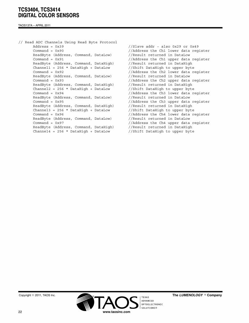
// Read ADC Channels Using Read Byte ProtocolAddress = 0x39 //Slave addr − also 0x29 or 0x49Command = 0x90 //Address the Ch1 lower data registerReadByte (Address, Command, DataLow) //Result returned in DataLowCommand = 0x91 //Address the Ch1 upper data registerReadByte (Address, Command, DataHigh) //Result returned in DataHighChannel1 = 256 * DataHigh + DataLow //Shift DataHigh to upper byteCommand = 0x92 //Address the Ch2 lower data registerReadByte (Address, Command, DataLow) //Result returned in DataLowCommand = 0x93 //Address the Ch2 upper data registerReadByte (Address, Command, DataHigh) //Result returned in DataHighChannel2 = 256 * DataHigh + DataLow //Shift DataHigh to upper byteCommand = 0x94 //Address the Ch3 lower data registerReadByte (Address, Command, DataLow) //Result returned in DataLowCommand = 0x95 //Address the Ch3 upper data registerReadByte (Address, Command, DataHigh) //Result returned in DataHighChannel3 = 256 * DataHigh + DataLow //Shift DataHigh to upper byteCommand = 0x96 //Address the Ch4 lower data registerReadByte (Address, Command, DataLow) //Result returned in DataLowCommand = 0x97 //Address the Ch4 upper data registerReadByte (Address, Command, DataHigh) //Result returned in DataHighChannel4 = 256 * DataHigh + DataLow //Shift DataHigh to upper byte
TCS3404, TCS3414DIGITAL COLOR SENSORS
TAOS137A − APRIL 2011
23
The LUMENOLOGY � Company�
�
Copyright � 2011, TAOS Inc.
www.taosinc.com
APPLICATION INFORMATION: SOFTWARE
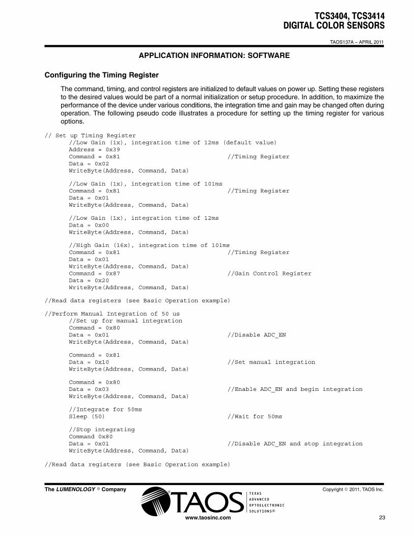
Configuring the Timing Register
The command, timing, and control registers are initialized to default values on power up. Setting these registersto the desired values would be part of a normal initialization or setup procedure. In addition, to maximize theperformance of the device under various conditions, the integration time and gain may be changed often duringoperation. The following pseudo code illustrates a procedure for setting up the timing register for variousoptions.
// Set up Timing Register//Low Gain (1x), integration time of 12ms (default value)Address = 0x39Command = 0x81 //Timing RegisterData = 0x02WriteByte(Address, Command, Data)
//Low Gain (1x), integration time of 101msCommand = 0x81 //Timing RegisterData = 0x01WriteByte(Address, Command, Data)
//Low Gain (1x), integration time of 12msData = 0x00WriteByte(Address, Command, Data)
//High Gain (16x), integration time of 101msCommand = 0x81 //Timing RegisterData = 0x01WriteByte(Address, Command, Data)Command = 0x87 //Gain Control RegisterData = 0x20WriteByte(Address, Command, Data)
//Read data registers (see Basic Operation example)
//Perform Manual Integration of 50 us//Set up for manual integrationCommand = 0x80Data = 0x01 //Disable ADC_ENWriteByte(Address, Command, Data)
Command = 0x81Data = 0x10 //Set manual integrationWriteByte(Address, Command, Data)
Command = 0x80Data = 0x03 //Enable ADC_EN and begin integrationWriteByte(Address, Command, Data)
//Integrate for 50msSleep (50) //Wait for 50ms
//Stop integratingCommand 0x80Data = 0x01 //Disable ADC_EN and stop integrationWriteByte(Address, Command, Data)
//Read data registers (see Basic Operation example)
TCS3404, TCS3414DIGITAL COLOR SENSORS
TAOS137A − APRIL 2011
24
�
�
Copyright � 2011, TAOS Inc. The LUMENOLOGY � Company
www.taosinc.com
APPLICATION INFORMATION: SOFTWARE
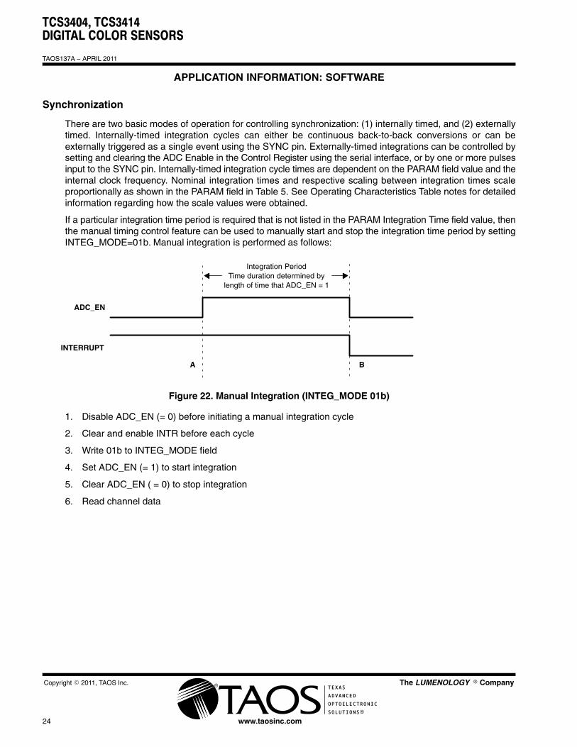
Synchronization
There are two basic modes of operation for controlling synchronization: (1) internally timed, and (2) externallytimed. Internally-timed integration cycles can either be continuous back-to-back conversions or can beexternally triggered as a single event using the SYNC pin. Externally-timed integrations can be controlled bysetting and clearing the ADC Enable in the Control Register using the serial interface, or by one or more pulsesinput to the SYNC pin. Internally-timed integration cycle times are dependent on the PARAM field value and theinternal clock frequency. Nominal integration times and respective scaling between integration times scaleproportionally as shown in the PARAM field in Table 5. See Operating Characteristics Table notes for detailedinformation regarding how the scale values were obtained.
If a particular integration time period is required that is not listed in the PARAM Integration Time field value, thenthe manual timing control feature can be used to manually start and stop the integration time period by settingINTEG_MODE=01b. Manual integration is performed as follows:
ADC_EN
Integration PeriodTime duration determined by
length of time that ADC_EN = 1
INTERRUPT
A B
Figure 22. Manual Integration (INTEG_MODE 01b)
1. Disable ADC_EN (= 0) before initiating a manual integration cycle
2. Clear and enable INTR before each cycle
3. Write 01b to INTEG_MODE field
4. Set ADC_EN (= 1) to start integration
5. Clear ADC_EN ( = 0) to stop integration
6. Read channel data

TCS3404, TCS3414DIGITAL COLOR SENSORS
TAOS137A − APRIL 2011
25
The LUMENOLOGY � Company�
�
Copyright � 2011, TAOS Inc.
www.taosinc.com
APPLICATION INFORMATION: SOFTWARE
When the INTEG_MODE field value is set to 10b, an externally-controlled synchronization input (SYNC) is usedto trigger the start of an integration period. The integration period starts on the rising edge of the SYNC pulse,triggers a single, internally-timed integration cycle, and continues until the Nominal Integration Time, as definedin the PARAM field, is completed.
SYNC IN
Integration PeriodTime duration determined by
PARAM field (nominalintegration time)
INTERRUPT
A B
NOTE: ADC_EN must be toggled (i.e. from high to low and back to high again) before next integration cycle
Figure 23. One-Shot Integration (INTEG_MODE 10b) Falling Edge
1. Enable ADC_EN (= 1)
2. Set PARAM for desired integration cycle (12ms, 100ms, or 400ms)
3. Set INTEG_MODE to 10b
4. Disable SYNC and clear INTR
5. Read channel data
TCS3404, TCS3414DIGITAL COLOR SENSORS
TAOS137A − APRIL 2011
26
�
�
Copyright � 2011, TAOS Inc. The LUMENOLOGY � Company
www.taosinc.com
APPLICATION INFORMATION: SOFTWARE
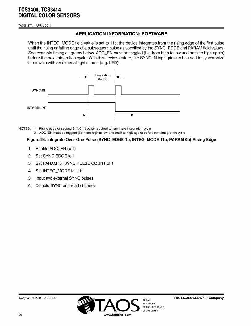
When the INTEG_MODE field value is set to 11b, the device integrates from the rising edge of the first pulseuntil the rising or falling edge of a subsequent pulse as specified by the SYNC_EDGE and PARAM field values.See example timing diagrams below. ADC_EN must be toggled (i.e. from high to low and back to high again)before the next integration cycle. With this device feature, the SYNC IN input pin can be used to synchronizethe device with an external light source (e.g. LED).
SYNC IN
IntegrationPeriod
INTERRUPT
A B
NOTES: 1. Rising edge of second SYNC IN pulse required to terminate integration cycle2. ADC_EN must be toggled (i.e. from high to low and back to high again) before next integration cycle
Figure 24. Integrate Over One Pulse (SYNC_EDGE 1b, INTEG_MODE 11b, PARAM 0b) Rising Edge
1. Enable ADC_EN (= 1)
2. Set SYNC EDGE to 1
3. Set PARAM for SYNC PULSE COUNT of 1
4. Set INTEG_MODE to 11b
5. Input two external SYNC pulses
6. Disable SYNC and read channels
TCS3404, TCS3414DIGITAL COLOR SENSORS
TAOS137A − APRIL 2011
27
The LUMENOLOGY � Company�
�
Copyright � 2011, TAOS Inc.
www.taosinc.com
APPLICATION INFORMATION: SOFTWARE
SYNC IN
INTERRUPT
A B
Integration Period
NOTE: ADC_EN must be toggled (i.e. from high to low and back to high again) before next integration cycle
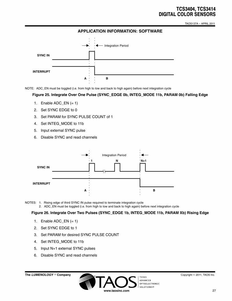
Figure 25. Integrate Over One Pulse (SYNC_EDGE 0b, INTEG_MODE 11b, PARAM 0b) Falling Edge
1. Enable ADC_EN (= 1)
2. Set SYNC EDGE to 0
3. Set PARAM for SYNC PULSE COUNT of 1
4. Set INTEG_MODE to 11b
5. Input external SYNC pulse
6. Disable SYNC and read channels
SYNC IN
Integration Period
INTERRUPT
A B
1 N N+1
NOTES: 1. Rising edge of third SYNC IN pulse required to terminate integration cycle2. ADC_EN must be toggled (i.e. from high to low and back to high again) before next integration cycle
Figure 26. Integrate Over Two Pulses (SYNC_EDGE 1b, INTEG_MODE 11b, PARAM Xb) Rising Edge
1. Enable ADC_EN (= 1)
2. Set SYNC EDGE to 1
3. Set PARAM for desired SYNC PULSE COUNT
4. Set INTEG_MODE to 11b
5. Input N+1 external SYNC pulses
6. Disable SYNC and read channels

TCS3404, TCS3414DIGITAL COLOR SENSORS
TAOS137A − APRIL 2011
28
�
�
Copyright � 2011, TAOS Inc. The LUMENOLOGY � Company
www.taosinc.com
APPLICATION INFORMATION: SOFTWARE
SYNC IN
IntegrationPeriod
INTERRUPT
A B
1 N
NOTE: ADC_EN must be toggled (i.e. from high to low and back to high again) before next integration cycle
Figure 27. Integrate Over Two Pulses (SYNC_EDGE 0b, INTEG_MODE 11b, PARAM Xb) Falling Edge
1. Enable ADC_EN (= 1)
2. Set SYNC EDGE to 0
3. Set PARAM for desired SYNC PULSE COUNT
4. Set INTEG_MODE to 11b
5. Input N external SYNC pulse(s)
6. Disable SYNC and read channels

TCS3404, TCS3414DIGITAL COLOR SENSORS
TAOS137A − APRIL 2011
29
The LUMENOLOGY � Company�
�
Copyright � 2011, TAOS Inc.
www.taosinc.com
APPLICATION INFORMATION: SOFTWARE
A synchronization input (SYNC IN) is supported to precisely start/stop sensor integration and synchronize withthe light source. The TIMING Register (01h) provides two synchronization modes of operation. The first modeof operation synchronizes the SYNC IN pin for one integration cycle as specified in the Timing Register (01h).When the rising edge of the signal is detected, the TCS3404/14 begins integration. The second modeaccumulates a specified number of SYNC IN pulses (see Timing Register) in which the minimum pulse widthis 50 μs. A pulse counter is used to count the rising and falling edges of the pulse(s) and precisely integrate thelight level when the SYNC IN pulse is high.
The following pseudo code illustrates a procedure for reading the TCS3404/14 device using the synchronizationfeature:
// Synchronize one integration cycle// See ”Basic Operation” to power−on and start device// See ”Configuring the Timing Register” to setup environment
Address = 0x39 //Slave addr − also 0x29 or 0x49Command = 0x81 //Set Command bit and address Timing RegisterData = 0x21 //Sync one 100ms integration period
//External SYNC IN pulse initiates 100ms integrationSleep (100)
// See ”Basic Operation” to read Data Registers using Byte or Word Protocol
// Synchronize N number of SYNC IN pulses// See ”Basic Operation” to power−on and start device// See ”Configuring the Timing Register” to setup environment
Address = 0x39 //Slave addr − also 0x29 or 0x49Command = 0x81 //Set Command bit and address Timing RegisterData = 0x30 //Integrate one SYNC IN pulse
//External SYNC IN pulse synchronizes integration// See ”Basic Operation” to read Data Registers using Byte or Word Protocol

TCS3404, TCS3414DIGITAL COLOR SENSORS
TAOS137A − APRIL 2011
30
�
�
Copyright � 2011, TAOS Inc. The LUMENOLOGY � Company
www.taosinc.com
APPLICATION INFORMATION: SOFTWARE
Interrupts
The interrupt feature of the TCS3404/14 device simplifies and improves system efficiency by eliminating theneed to poll the sensor for a light intensity value. Interrupt mode is determined by the INTR field in the InterruptControl Register. The interrupt feature may be disabled by writing a field value of 00h to the Interrupt ControlRegister (02h) so that polling can be performed.
The versatility of the interrupt feature provides many options for interrupt configuration and usage. The primarypurpose of the interrupt function is to signal a meaningful change in light intensity. However, it also be used asan end-of-conversion signal. The concept of a meaningful change can be defined by the user both in terms oflight intensity and time, or persistence, of that change in intensity. The TCS3404/14 device implements two16-bit-wide interrupt threshold registers that allow the user to define thresholds above and below a desired lightlevel. An interrupt will then be generated when the value of a conversion exceeds either of these limits. Forsimplicity of programming, the threshold comparison uses the Interrupt Source Register (03h) to select whichADC channel (1 through 4) to generate the interrupt. This simplifies calculation of thresholds that are based ona percent of the current light level. For example, it is adequate to use only one channel (e.g. green channel) whencalculating light intensity differences since, for a given light source, channel values are linearly proportional toeach other and thus each value scales linearly with light intensity.
To further control when an interrupt occurs, the TCS3404/14 device provides an interrupt persistence feature.This feature allows the user to specify the length in time of the number of consecutive ADC channel values forwhich a light intensity exceeding either interrupt threshold must persist before actually generating an interrupt.This can be used to prevent transient changes in light intensity from generating an unwanted interrupt. SeeTable 6 regarding the number of timer values provided.
Two different interrupt styles are available: Level and SMBus Alert. The difference between these two interruptstyles is how they are cleared. Both result in the interrupt line going active low and remaining low until theinterrupt is cleared. A level style interrupt is cleared by setting the Interrupt Clear field in the the COMMANDregister to 11b. The SMBus Alert style interrupt is cleared by an Alert Response as described in the InterruptControl Register section and SMBus specification.
To configure the interrupt as an end−of−conversion signal so that every ADC integration cycle generates aninterrupt, the interrupt PERSIST field in the Interrupt Control Register (02h) is set to 000b. Either Level or SMBusAlert style can be used. An interrupt will be generated upon completion of each conversion. The interruptthreshold registers are ignored. The following example illustrates the configuration of a level interrupt:
// Set up end−of−conversion interrupt, Level styleAddress = 0x39 //Slave address − alternatively 0x29 or 0x49Command = 0x83 //Interrupt Source RegisterData = 0x01 //Select Channel 2WriteByte(Address, Command, Data)
Command = 0x82 //Address Interrupt RegisterData = 0x10 //Level style, every ADC cycleWriteByte(Address, Command, Data)

TCS3404, TCS3414DIGITAL COLOR SENSORS
TAOS137A − APRIL 2011
31
The LUMENOLOGY � Company�
�
Copyright � 2011, TAOS Inc.
www.taosinc.com
APPLICATION INFORMATION: SOFTWARE
The following example pseudo code illustrates the configuration of an SMB-Alert style interrupt when the lightintensity changes 20% from the current value, and persists for 2.5 seconds:
//Assume Interrupt Source as Channel 1//Read current light levelAddress = 0x39 //Slave address − alternatively 0x29 or 0x49Command = 0xB0 //Set Command bit and SMBus Word readReadWord (Address, Command, DataLow, DataHigh)Channel1 = (256 * DataHigh) + DataLow//Calculate upper and lower thresholdsT_Upper = Channel1 + (0.2 * Channel1)T_Lower = Channel1 − (0.2 * Channel1)//Write the lower threshold registerCommand = 0xA8 //Address lower threshold register, set Word BitWriteWord (Address, Command, T_Lower.LoByte, T_Lower.HiByte)//Write the upper threshold registerCommand = 0xAA //Address upper threshold register, set Word bitWriteWord (Address, Command, T_Upper.LoByte, T_Upper.HiByte)//Enable interruptCommand = 0x82 //Address interrupt registerData = 0x24 //SMBAlert style, Persist 2.5 secondsWriteByte(Address, Command, Data)
In order to generate an interrupt on demand during system test or debug, a test mode (INTR = 11) can be used.The following example illustrates how to generate an interrupt on demand:
// Generate an interruptAddress = 0x39 //Slave address alternately 0x29 or 0x49Command = 0x82 //Address Interrupt Control RegisterData = 0x30 //Test interruptWriteByte(Address, Command, Data)
//Interrupt line should now be low

TCS3404, TCS3414DIGITAL COLOR SENSORS
TAOS137A − APRIL 2011
32
�
�
Copyright � 2011, TAOS Inc. The LUMENOLOGY � Company
www.taosinc.com
APPLICATION INFORMATION: HARDWARE
Power Supply Decoupling and Application Hardware Circuit
The power supply lines must be decoupled with a 0.1 μF capacitor placed as close to the device package aspossible (Figure 28). The bypass capacitor should have low effective series resistance (ESR) and low effectiveseries inductance (ESI), such as the common ceramic types, which provide a low impedance path to groundat high frequencies to handle transient currents caused by internal logic switching.
TCS3404/14
VBUS VDD
0.1 �F
RP RP
SCL
SDA
RPI
INT
Figure 28. Bus Pull-Up Resistors
Pull-up resistors (Rp) maintain the SDA and SCL lines at a high level when the bus is free and ensure the signalsare pulled up from a low to a high level within the required rise time. For a complete description of I2C maximumand minimum Rp values, please review the NXP I2C design specification at http://www.i2c−bus.org/references/.
A pull-up resistor (RPI) is also required for the interrupt (INT), which functions as a wired-AND signal in a similarfashion to the SCL and SDA lines. A typical impedance value between 10 kΩ and 100 kΩ can be used. Pleasenote that while the figure above shows INT being pulled up to VDD, the interrupt can optionally be pulled up toVBUS.
TCS3404, TCS3414DIGITAL COLOR SENSORS
TAOS137A − APRIL 2011
33
The LUMENOLOGY � Company�
�
Copyright � 2011, TAOS Inc.
www.taosinc.com
APPLICATION INFORMATION: HARDWARE
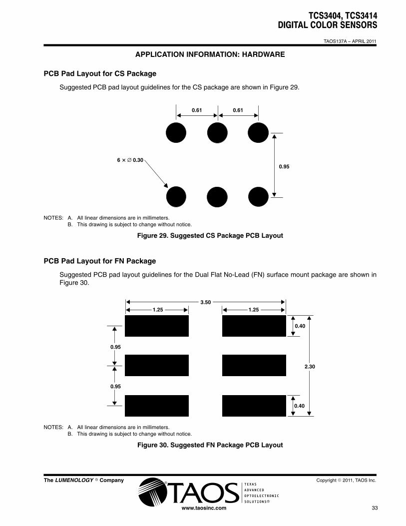
PCB Pad Layout for CS Package
Suggested PCB pad layout guidelines for the CS package are shown in Figure 29.
6 � � 0.300.95
0.61 0.61
NOTES: A. All linear dimensions are in millimeters.B. This drawing is subject to change without notice.
Figure 29. Suggested CS Package PCB Layout
PCB Pad Layout for FN Package
Suggested PCB pad layout guidelines for the Dual Flat No-Lead (FN) surface mount package are shown inFigure 30.
0.40
3.50
0.40
1.25
2.30
0.95
1.25
0.95
NOTES: A. All linear dimensions are in millimeters.B. This drawing is subject to change without notice.
Figure 30. Suggested FN Package PCB Layout
TCS3404, TCS3414DIGITAL COLOR SENSORS
TAOS137A − APRIL 2011
34
�
�
Copyright � 2011, TAOS Inc. The LUMENOLOGY � Company
www.taosinc.com
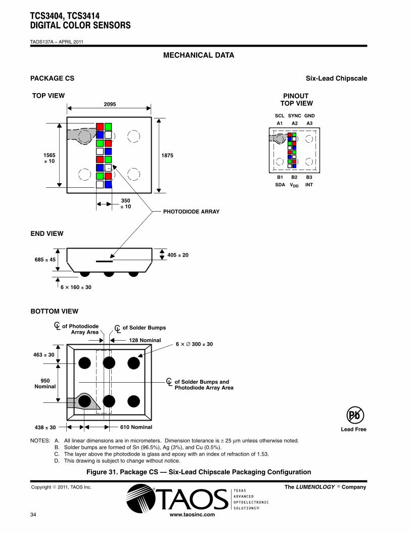
MECHANICAL DATA
PACKAGE CS Six-Lead Chipscale
950Nominal
350� 10
1565� 10
2095
463 � 30
610 Nominal438 � 30
TOP VIEW
BOTTOM VIEW
END VIEW
Lead Free
Pb
6 � � 300 � 30
PINOUT TOP VIEW
SCL
A1
SYNC
A2
GND
A3
B1
SDA
B2
VDD
B3
INT
PHOTODIODE ARRAY
1875
128 Nominal
CL of Solder Bumps andPhotodiode Array Area
6 � 160 � 30
405 � 20685 � 45
CL of Solder BumpsCL of PhotodiodeArray Area
NOTES: A. All linear dimensions are in micrometers. Dimension tolerance is ± 25 μm unless otherwise noted.B. Solder bumps are formed of Sn (96.5%), Ag (3%), and Cu (0.5%).C. The layer above the photodiode is glass and epoxy with an index of refraction of 1.53.D. This drawing is subject to change without notice.
Figure 31. Package CS — Six-Lead Chipscale Packaging Configuration

TCS3404, TCS3414DIGITAL COLOR SENSORS
TAOS137A − APRIL 2011
35
The LUMENOLOGY � Company�
�
Copyright � 2011, TAOS Inc.
www.taosinc.com
MECHANICAL DATA
PACKAGE FN Dual Flat No-Lead
203 � 8
6 GND
5 Vdd
4 INT
SCL 1
SYNC 2
SDA 3
TOP VIEW
SIDE VIEW
BOTTOM VIEW300� 50
950
3000� 100
3000� 100
PIN 1
PIN 1
END VIEW
650 � 50
PIN OUTTOPVIEW
950 � 150
PHOTODIODE ARRAY
295Nominal
Lead Free
Pb
350 � 10
1565� 10
128 Nominal
CL of Solder ContactsCL of Photodiode
Array Area(Note B)
CL of Solder Contacts andPhotodiode Array Area (Note B)
NOTES: A. All linear dimensions are in micrometers. Dimension tolerance is ± 20 μm unless otherwise noted.B. The die is centered within the package within a tolerance of ± 3 mils.C. Package top surface is molded with an electrically nonconductive clear plastic compound having an index of refraction of 1.55.D. Contact finish is copper alloy A194 with pre-plated NiPdAu lead finish.E. This package contains no lead (Pb).F. This drawing is subject to change without notice.
Figure 32. Package FN — Dual Flat No-Lead Packaging Configuration
TCS3404, TCS3414DIGITAL COLOR SENSORS
TAOS137A − APRIL 2011
36
�
�
Copyright � 2011, TAOS Inc. The LUMENOLOGY � Company
www.taosinc.com
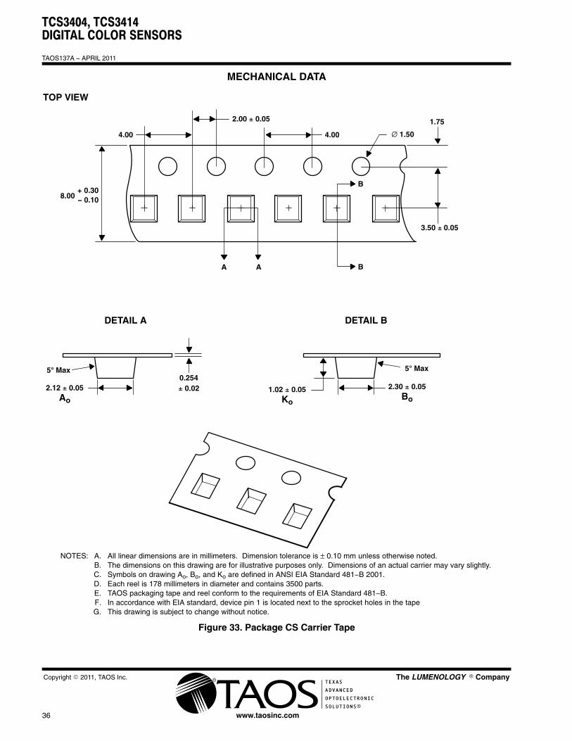
MECHANICAL DATA
TOP VIEW
DETAIL A
2.12 � 0.05Ao
0.254� 0.02
5� Max
4.00
8.00
3.50 � 0.05
� 1.504.00
2.00 � 0.05
+ 0.30− 0.10
1.75
B
BA A
DETAIL B
2.30 � 0.05Bo
5� Max
1.02 � 0.05Ko
NOTES: A. All linear dimensions are in millimeters. Dimension tolerance is ± 0.10 mm unless otherwise noted.B. The dimensions on this drawing are for illustrative purposes only. Dimensions of an actual carrier may vary slightly.C. Symbols on drawing Ao, Bo, and Ko are defined in ANSI EIA Standard 481−B 2001.D. Each reel is 178 millimeters in diameter and contains 3500 parts.E. TAOS packaging tape and reel conform to the requirements of EIA Standard 481−B.F. In accordance with EIA standard, device pin 1 is located next to the sprocket holes in the tapeG. This drawing is subject to change without notice.
Figure 33. Package CS Carrier Tape
TCS3404, TCS3414DIGITAL COLOR SENSORS
TAOS137A − APRIL 2011
37
The LUMENOLOGY � Company�
�
Copyright � 2011, TAOS Inc.
www.taosinc.com
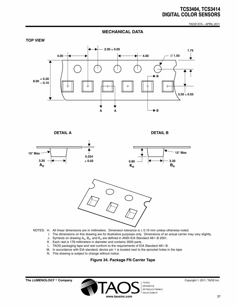
MECHANICAL DATA
TOP VIEW
DETAIL A
3.30Ao
0.254� 0.02
10� Max
4.00
8.00
3.50 � 0.05
� 1.504.00
2.00 � 0.05
+ 0.30− 0.10
1.75
B
BA A
DETAIL B
3.30Bo
12� Max
0.80Ko
NOTES: H. All linear dimensions are in millimeters. Dimension tolerance is ± 0.10 mm unless otherwise noted.I. The dimensions on this drawing are for illustrative purposes only. Dimensions of an actual carrier may vary slightly.J. Symbols on drawing Ao, Bo, and Ko are defined in ANSI EIA Standard 481−B 2001.K. Each reel is 178 millimeters in diameter and contains 3500 parts.L. TAOS packaging tape and reel conform to the requirements of EIA Standard 481−B.
M. In accordance with EIA standard, device pin 1 is located next to the sprocket holes in the tapeN. This drawing is subject to change without notice.
Figure 34. Package FN Carrier Tape
TCS3404, TCS3414DIGITAL COLOR SENSORS
TAOS137A − APRIL 2011
38
�
�
Copyright � 2011, TAOS Inc. The LUMENOLOGY � Company
www.taosinc.com
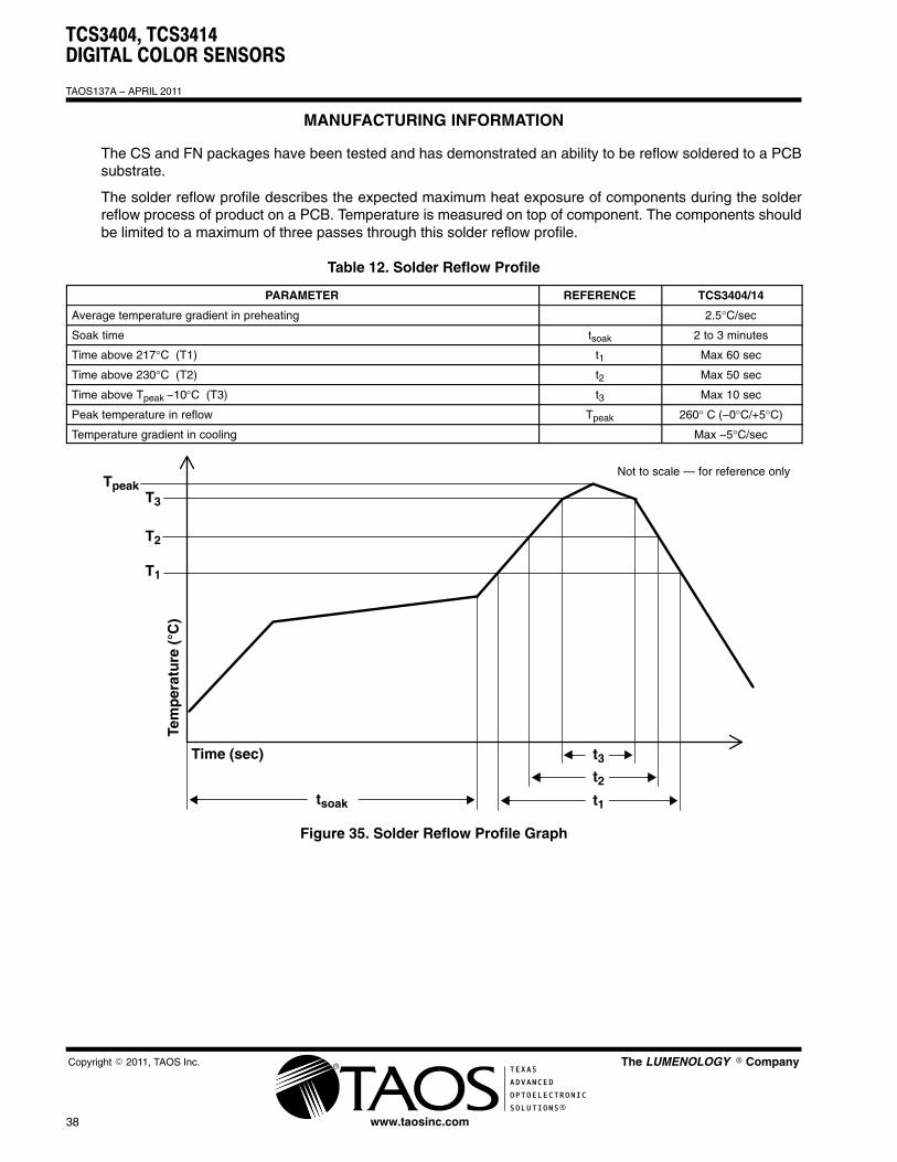
MANUFACTURING INFORMATION
The CS and FN packages have been tested and has demonstrated an ability to be reflow soldered to a PCBsubstrate.
The solder reflow profile describes the expected maximum heat exposure of components during the solderreflow process of product on a PCB. Temperature is measured on top of component. The components shouldbe limited to a maximum of three passes through this solder reflow profile.
Table 12. Solder Reflow Profile
PARAMETER REFERENCE TCS3404/14
Average temperature gradient in preheating 2.5°C/sec
Soak time tsoak 2 to 3 minutes
Time above 217°C (T1) t1 Max 60 sec
Time above 230°C (T2) t2 Max 50 sec
Time above Tpeak −10°C (T3) t3 Max 10 sec
Peak temperature in reflow Tpeak 260° C (−0°C/+5°C)
Temperature gradient in cooling Max −5°C/sec
t3t2t1tsoak
T3
T2
T1
TpeakNot to scale — for reference only
Time (sec)
Tem
per
atu
re (�C
)
Figure 35. Solder Reflow Profile Graph

TCS3404, TCS3414DIGITAL COLOR SENSORS
TAOS137A − APRIL 2011
39
The LUMENOLOGY � Company�
�
Copyright � 2011, TAOS Inc.
www.taosinc.com
MANUFACTURING INFORMATION
Moisture Sensitivity
Optical characteristics of the device can be adversely affected during the soldering process by the release andvaporization of moisture that has been previously absorbed into the package molding compound. To ensure thepackage molding compound contains the smallest amount of absorbed moisture possible, each device isdry-baked prior to being packed for shipping. Devices are packed in a sealed aluminized envelope with silicagel to protect them from ambient moisture during shipping, handling, and storage before use.
CS Package
The CS package has been assigned a moisture sensitivity level of MSL 2 and the devices should be stored underthe following conditions:
Temperature Range 5°C to 50°CRelative Humidity 60% maximumFloor Life 1 year out of bag at ambient < 30°C / 60% RH
Rebaking will be required if the aluminized envelope has been open for more than 1 year. If rebaking is required,it should be done at 50°C for 12 hours.
FN Package
The FN package has been assigned a moisture sensitivity level of MSL 3 and the devices should be stored underthe following conditions:
Temperature Range 5°C to 50°CRelative Humidity 60% maximumTotal Time 12 months from the date code on the aluminized envelope — if unopenedOpened Time 168 hours or fewer
Rebaking will be required if the devices have been stored unopened for more than 12 months or if the aluminizedenvelope has been open for more than 168 hours. If rebaking is required, it should be done at 50°C for 12 hours.

TCS3404, TCS3414DIGITAL COLOR SENSORS
TAOS137A − APRIL 2011
40
�
�
Copyright � 2011, TAOS Inc. The LUMENOLOGY � Company
www.taosinc.com
PRODUCTION DATA — information in this document is current at publication date. Products conform tospecifications in accordance with the terms of Texas Advanced Optoelectronic Solutions, Inc. standardwarranty. Production processing does not necessarily include testing of all parameters.
LEAD-FREE (Pb-FREE) and GREEN STATEMENTPb-Free (RoHS) TAOS’ terms Lead-Free or Pb-Free mean semiconductor products that are compatible with the currentRoHS requirements for all 6 substances, including the requirement that lead not exceed 0.1% by weight in homogeneousmaterials. Where designed to be soldered at high temperatures, TAOS Pb-Free products are suitable for use in specifiedlead-free processes.
Green (RoHS & no Sb/Br) TAOS defines Green to mean Pb-Free (RoHS compatible), and free of Bromine (Br) andAntimony (Sb) based flame retardants (Br or Sb do not exceed 0.1% by weight in homogeneous material).
Important Information and Disclaimer The information provided in this statement represents TAOS’ knowledge andbelief as of the date that it is provided. TAOS bases its knowledge and belief on information provided by third parties,and makes no representation or warranty as to the accuracy of such information. Efforts are underway to better integrateinformation from third parties. TAOS has taken and continues to take reasonable steps to provide representativeand accurate information but may not have conducted destructive testing or chemical analysis on incoming materials andchemicals. TAOS and TAOS suppliers consider certain information to be proprietary, and thus CAS numbers and otherlimited information may not be available for release.
NOTICETexas Advanced Optoelectronic Solutions, Inc. (TAOS) reserves the right to make changes to the products contained in thisdocument to improve performance or for any other purpose, or to discontinue them without notice. Customers are advisedto contact TAOS to obtain the latest product information before placing orders or designing TAOS products into systems.
TAOS assumes no responsibility for the use of any products or circuits described in this document or customer productdesign, conveys no license, either expressed or implied, under any patent or other right, and makes no representation thatthe circuits are free of patent infringement. TAOS further makes no claim as to the suitability of its products for any particularpurpose, nor does TAOS assume any liability arising out of the use of any product or circuit, and specifically disclaims anyand all liability, including without limitation consequential or incidental damages.
TEXAS ADVANCED OPTOELECTRONIC SOLUTIONS, INC. PRODUCTS ARE NOT DESIGNED OR INTENDED FORUSE IN CRITICAL APPLICATIONS IN WHICH THE FAILURE OR MALFUNCTION OF THE TAOS PRODUCT MAYRESULT IN PERSONAL INJURY OR DEATH. USE OF TAOS PRODUCTS IN LIFE SUPPORT SYSTEMS IS EXPRESSLYUNAUTHORIZED AND ANY SUCH USE BY A CUSTOMER IS COMPLETELY AT THE CUSTOMER’S RISK.
LUMENOLOGY, TAOS, the TAOS logo, and Texas Advanced Optoelectronic Solutions are registered trademarks of Texas AdvancedOptoelectronic Solutions Incorporated.