digital design - higher education | pearson · pdf file9.2 experiment 1: binary and decimal...
TRANSCRIPT

Digital DesignWith an Introduction to the Verilog HDL
A01_MANO4208_05_SE_FM.indd iA01_MANO4208_05_SE_FM.indd i 21/11/11 1:18 PM21/11/11 1:18 PM
©2013 Pearson Education, Inc., Upper Saddle River, NJ 07458. All Rights Reserved

A01_MANO4208_05_SE_FM.indd iiA01_MANO4208_05_SE_FM.indd ii 21/11/11 1:18 PM21/11/11 1:18 PM
©2013 Pearson Education, Inc., Upper Saddle River, NJ 07458. All Rights Reserved

Digital Design With an Introduction to the Verilog HDL
FIFTH EDITION
M. Morris Mano Emeritus Professor of Computer Engineering
California State University, Los Angeles
Michael D. Ciletti Emeritus Professor of Electrical and Computer Engineering
University of Colorado at Colorado Springs
Upper Saddle River Boston Columbus San Franciso New YorkIndianapolis London Toronto Sydney Singapore Tokyo Montreal
Dubai Madrid Hong Kong Mexico City Munich Paris Amsterdam Cape Town
A01_MANO4208_05_SE_FM.indd iiiA01_MANO4208_05_SE_FM.indd iii 21/11/11 1:18 PM21/11/11 1:18 PM
©2013 Pearson Education, Inc., Upper Saddle River, NJ 07458. All Rights Reserved

Library of Congress Cataloging-in-Publication Data
Mano, M. Morris, 1927–
Digital design : with a introduction to the verilog hdl / M. Morris Mano, Michael D. Ciletti.—5th ed.
p. cm.
Includes index.
ISBN-13: 978-0-13-277420-8
ISBN-10: 0-13-277420-8
1. Electronic digital computers—Circuits. 2. Logic circuits. 3. Logic design. 4. Digital integrated
circuits. I. Ciletti, Michael D. II. Title.
TK7888.3.M343 2011
621.39'5—dc23
2011039094
Vice President and Editorial Director, ECS:
Marcia J. HortonExecutive Editor: Andrew GilfillanVice-President, Production: Vince O’BrienExecutive Marketing Manager: Tim GalliganMarketing Assistant: Jon BryantPermissions Project Manager: Karen SanatarSenior Managing Editor: Scott DisannoProduction Project Manager/Editorial Production
Manager: Greg Dulles
Cover Designer: Jayne ConteCover Photo: Michael D. CilettiComposition: Jouve India Private LimitedFull-Service Project Management: Jouve India Private LimitedPrinter/Binder: Edwards BrothersTypeface: Times Ten 10/12
Copyright © 2013, 2007, 2002, 1991, 1984 Pearson Education, Inc., publishing as Prentice Hall, One Lake Street, Upper Saddle River, New Jersey 07458. All rights reserved. Manufactured in the United States of America. This publication is
protected by Copyright, and permission should be obtained from the publisher prior to any prohibited reproduction,
storage in a retrieval system, or transmission in any form or by any means, electronic, mechanical, photocopying,
recording, or likewise. To obtain permission(s) to use material from this work, please submit a written request to
Pearson Education, Inc., Permissions Department, One Lake Street, Upper Saddle River, New Jersey 07458.
Many of the designations by manufacturers and seller to distinguish their products are claimed as trademarks. Where
those designations appear in this book, and the publisher was aware of a trademark claim, the designations have been
printed in initial caps or all caps.
All rights reserved. No part of this book may be reproduced, in any form or by any means, without permission in writing
from the publisher.
Verilogger Pro and SynaptiCAD are trademarks of SynaptiCAD, Inc., Blacksburg, VA 24062–0608.
The author and publisher of this book have used their best efforts in preparing this book. These efforts include the
development, research, and testing of the theories and programs to determine their effectiveness. The author and
publisher make no warranty of any kind, expressed or implied, with regard to these programs or the documentation
contained in this book. The author and publisher shall not be liable in any event for incidental or consequential
damages in connection with, or arising out of, the furnishing, performance, or use of these programs.
About the cover: “Spider Rock in Canyon de Chelley,” Chinle, Arizona, USA, January 2011. Photograph courtesy of mdc
Images, LLC (www.mdcilettiphotography.com). Used by permission.
Pearson Education Ltd., LondonPearson Education Singapore, Pte. Ltd
Pearson Education Canada, Inc.
Pearson Education—Japan
Pearson Education Australia PTY, Limited
Pearson Education North Asia, Ltd., Hong KongPearson Educación de Mexico, S.A. de C.V.
Pearson Education Malaysia, Pte. Ltd.
Pearson Education, Inc., Upper Saddle River, New Jersey
10 9 8 7 6 5 4 3 2 1
ISBN-13: 978-0-13-277420-8
ISBN-10: 0-13-277420-8
A01_MANO4208_05_SE_FM.indd ivA01_MANO4208_05_SE_FM.indd iv 21/11/11 1:18 PM21/11/11 1:18 PM
©2013 Pearson Education, Inc., Upper Saddle River, NJ 07458. All Rights Reserved

v
P r e f a c e i x
1 D i g i t a l S y s t e m s a n d B i n a r y N u m b e r s 1
1.1 Digital Systems 1 1.2 Binary Numbers 3 1.3 Number‐Base Conversions 6 1.4 Octal and Hexadecimal Numbers 8 1.5 Complements of Numbers 10 1.6 Signed Binary Numbers 14 1.7 Binary Codes 18 1.8 Binary Storage and Registers 27 1.9 Binary Logic 30
2 B o o l e a n A l g e b r a a n d L o g i c G a t e s 3 8
2.1 Introduction 38 2.2 Basic Definitions 38 2.3 Axiomatic Definition of Boolean Algebra 40 2.4 Basic Theorems and Properties of Boolean Algebra 43 2.5 Boolean Functions 46 2.6 Canonical and Standard Forms 51 2.7 Other Logic Operations 58 2.8 Digital Logic Gates 60 2.9 Integrated Circuits 66
Contents
A01_MANO4208_05_SE_FM.indd vA01_MANO4208_05_SE_FM.indd v 21/11/11 1:18 PM21/11/11 1:18 PM
©2013 Pearson Education, Inc., Upper Saddle River, NJ 07458. All Rights Reserved

vi Contents
3 G a t e ‐ L e v e l M i n i m i z a t i o n 7 3
3.1 Introduction 73 3.2 The Map Method 73 3.3 Four‐Variable K-Map 80 3.4 Product‐of‐Sums Simplification 84 3.5 Don’t‐Care Conditions 88 3.6 NAND and NOR Implementation 90 3.7 Other Two‐Level Implementations 97 3.8 Exclusive‐OR Function 103 3.9 Hardware Description Language 108
4 C o m b i n a t i o n a l L o g i c 1 2 5
4.1 Introduction 125 4.2 Combinational Circuits 125 4.3 Analysis Procedure 126 4.4 Design Procedure 129 4.5 Binary Adder‐Subtractor 133 4.6 Decimal Adder 144 4.7 Binary Multiplier 146 4.8 Magnitude Comparator 148 4.9 Decoders 150 4.10 Encoders 155 4.11 Multiplexers 158 4.12 HDL Models of Combinational Circuits 164
5 S y n c h r o n o u s S e q u e n t i a l L o g i c 1 9 0
5.1 Introduction 190 5.2 Sequential Circuits 190 5.3 Storage Elements: Latches 193 5.4 Storage Elements: Flip‐Flops 196 5.5 Analysis of Clocked Sequential Circuits 204 5.6 Synthesizable HDL Models of Sequential Circuits 217 5.7 State Reduction and Assignment 231 5.8 Design Procedure 236
6 R e g i s t e r s a n d C o u n t e r s 2 5 5
6.1 Registers 255 6.2 Shift Registers 258 6.3 Ripple Counters 266 6.4 Synchronous Counters 271 6.5 Other Counters 278 6.6 HDL for Registers and Counters 283
A01_MANO4208_05_SE_FM.indd viA01_MANO4208_05_SE_FM.indd vi 21/11/11 1:18 PM21/11/11 1:18 PM
©2013 Pearson Education, Inc., Upper Saddle River, NJ 07458. All Rights Reserved
Contents vii
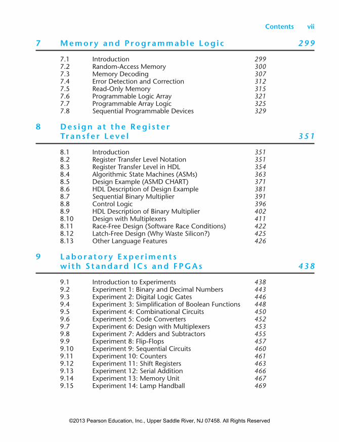
7 M e m o r y a n d P r o g r a m m a b l e L o g i c 2 9 9
7.1 Introduction 299 7.2 Random‐Access Memory 300 7.3 Memory Decoding 307 7.4 Error Detection and Correction 312 7.5 Read‐Only Memory 315 7.6 Programmable Logic Array 321 7.7 Programmable Array Logic 325 7.8 Sequential Programmable Devices 329
8 D e s i g n a t t h e R e g i s t e r Tr a n s f e r L e v e l 3 5 1
8.1 Introduction 351 8.2 Register Transfer Level Notation 351 8.3 Register Transfer Level in HDL 354 8.4 Algorithmic State Machines (ASMs) 363 8.5 Design Example (ASMD CHART) 371 8.6 HDL Description of Design Example 381 8.7 Sequential Binary Multiplier 391 8.8 Control Logic 396 8.9 HDL Description of Binary Multiplier 402 8.10 Design with Multiplexers 411 8.11 Race‐Free Design (Software Race Conditions) 422 8.12 Latch‐Free Design (Why Waste Silicon?) 425 8.13 Other Language Features 426
9 L a b o r a t o r y E x p e r i m e n t s w i t h S t a n d a r d I C s a n d F P G A s 4 3 8
9.1 Introduction to Experiments 438 9.2 Experiment 1: Binary and Decimal Numbers 443 9.3 Experiment 2: Digital Logic Gates 446 9.4 Experiment 3: Simplification of Boolean Functions 448 9.5 Experiment 4: Combinational Circuits 450 9.6 Experiment 5: Code Converters 452 9.7 Experiment 6: Design with Multiplexers 453 9.8 Experiment 7: Adders and Subtractors 455 9.9 Experiment 8: Flip‐Flops 457 9.10 Experiment 9: Sequential Circuits 460 9.11 Experiment 10: Counters 461 9.12 Experiment 11: Shift Registers 463 9.13 Experiment 12: Serial Addition 466 9.14 Experiment 13: Memory Unit 467 9.15 Experiment 14: Lamp Handball 469
A01_MANO4208_05_SE_FM.indd viiA01_MANO4208_05_SE_FM.indd vii 21/11/11 1:18 PM21/11/11 1:18 PM
©2013 Pearson Education, Inc., Upper Saddle River, NJ 07458. All Rights Reserved
viii Contents
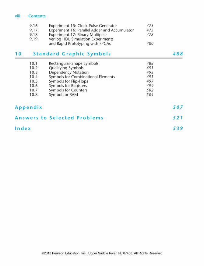
9.16 Experiment 15: Clock‐Pulse Generator 473 9.17 Experiment 16: Parallel Adder and Accumulator 475 9.18 Experiment 17: Binary Multiplier 478 9.19 Verilog HDL Simulation Experiments
and Rapid Prototyping with FPGAs 480
1 0 S t a n d a r d G r a p h i c S y m b o l s 4 8 8
10.1 Rectangular‐Shape Symbols 488 10.2 Qualifying Symbols 491 10.3 Dependency Notation 493 10.4 Symbols for Combinational Elements 495 10.5 Symbols for Flip‐Flops 497 10.6 Symbols for Registers 499 10.7 Symbols for Counters 502 10.8 Symbol for RAM 504
A p p e n d i x 5 0 7
A n s w e r s t o S e l e c t e d P r o b l e m s 5 2 1
I n d e x 5 3 9
A01_MANO4208_05_SE_FM.indd viiiA01_MANO4208_05_SE_FM.indd viii 21/11/11 1:18 PM21/11/11 1:18 PM
©2013 Pearson Education, Inc., Upper Saddle River, NJ 07458. All Rights Reserved

ix
Since the fourth edition of Digital Design, the commercial availability of devices using
digital technology to receive, manipulate, and transmit information seems to have
exploded. Cell phones and handheld devices of various kinds offer new, competing
features almost daily. Underneath the attractive graphical user interface of all of these
devices sits a digital system that processes data in a binary format. The theoretical
foundations of these systems have not changed much; indeed, one could argue that
the stability of the core theory, coupled with modern design tools, has promoted the
widespread response of manufacturers to the opportunities of the marketplace. Con-
sequently, our refinement of our text has been guided by the need to equip our grad-
uates with a solid understanding of digital machines and to introduce them to the
methodology of modern design.
This edition of Digital Design builds on the previous four editions, and the feedback
of the team of reviewers who helped set a direction for our presentation. The focus of
the text has been sharpened to more closely reflect the content of a foundation course
in digital design and the mainstream technology of today’s digital systems: CMOS
circuits. The intended audience is broad, embracing students of computer science, com-
puter engineering, and electrical engineering. The key elements that the book focuses
include (1) Boolean logic, (2) logic gates used by designers, (3) synchronous finite state
machines, and (4) datapath controller design—all from a perspective of designing dig-
ital systems. This focus led to elimination of material more suited for a course in elec-
tronics. So the reader will not find here content for asynchronous machines or
descriptions of bipolar transistors. Additionally, the widespread availability of web‐
based ancillary material prompted us to limit our discussion of field programmable
gate arrays (FPGAs) to an introduction of devices offered by only one manufacturer,
rather than two. Today’s designers rely heavily on hardware description languages
Preface
A01_MANO4208_05_SE_FM.indd ixA01_MANO4208_05_SE_FM.indd ix 21/11/11 1:18 PM21/11/11 1:18 PM
©2013 Pearson Education, Inc., Upper Saddle River, NJ 07458. All Rights Reserved

x Preface
(HDLs), and this edition of the book gives greater attention to their use and presents
what we think is a clear development of a design methodology using the Verilog HDL.
M U LT I ‐ M O D A L L E A R N I N G
Digital Design supports a multimodal approach to learning. The so‐called VARK char-
acterization of learning modalities identifies four major modes by which humans learn:
(V) visual, (A) aural, (R) reading, and (K) kinesthetic. In hindsight, we note that the
relatively high level of illustrations and graphical content of our text addresses the visual
(V) component of VARK; discussions and numerous examples address the reading (R)
component. Students who exploit the availability of free simulators to work assignments
are led through a kinesthetic (K) learning experience, including the positive feedback
and delight of designing a logic system that works. The remaining element of VARK, the
aural/auditory (A) experience, is left to the instructor. We have provided an abundance
of material and examples to support classroom lectures. Thus, a course in digital design,
using Digital Design, can provide a rich, balanced learning experience and address all
the modes identified by VARK.
For those who might still question the presentation and use of HDLs in a first course
in digital design, we note that industry has largely abandoned schematic‐based design
entry, a style which emerged in the 1980s, during the nascent development of CAD tools
for integrated circuit (IC) design. Schematic entry creates a representation of functional-
ity that is implicit in the layout of the schematic. Unfortunately, it is difficult for anyone
in a reasonable amount of time to determine the functionality represented by the sche-
matic of a logic circuit without having been instrumental in its construction, or without
having additional documentation expressing the design intent. Consequently, industry
has migrated to HDLs (e.g., Verilog) to describe the functionality of a design and to serve
as the basis for documenting, simulating, testing, and synthesizing the hardware imple-
mentation of the design in a standard cell‐based ASIC or an FPGA. The utility of a
schematic depends on the careful, detailed documentation of a carefully constructed
hierarchy of design modules. In the old paradigm, designers relied upon their years of
experience to create a schematic of a circuit to implement functionality. In today’s design
flow, designers using HDLs can express functionality directly and explicitly, without years
of accumulated experience, and use synthesis tools to generate the schematic as a by‐
product, automatically. Industry practices arrived here because schematic entry dooms
us to inefficiency, if not failure, in understanding and designing large, complex ICs.
We note, again in this edition, that introducing HDLs in a first course in designing
digital circuits is not intended to replace fundamental understanding of the building blocks
of such circuits or to eliminate a discussion of manual methods of design. It is still essential
for a student to understand how hardware works . Thus, we retain a thorough treatment of
combinational and sequential logic devices. Manual design practices are presented, and
their results are compared with those obtained with a HDL‐based paradigm. What we are
presenting, however, is an emphasis on how hardware is designed, to better prepare a
student for a career in today’s industry, where HDL‐based design practices are dominant.
A01_MANO4208_05_SE_FM.indd xA01_MANO4208_05_SE_FM.indd x 21/11/11 1:18 PM21/11/11 1:18 PM
©2013 Pearson Education, Inc., Upper Saddle River, NJ 07458. All Rights Reserved

Preface xi
F L E X I B I L I T Y
The sequence of topics in the text can accommodate courses that adhere to traditional,
manual‐based, treatments of digital design, courses that treat design using an HDL, and
courses that are in transition between or blend the two approaches. Because modern
synthesis tools automatically perform logic minimization, Karnaugh maps and related
topics in optimization can be presented at the beginning of a treatment of digital design,
or they can be presented after circuits and their applications are examined and simulated
with an HDL. The text includes both manual and HDL‐based design examples. Our end‐
of‐chapter problems further facilitate this flexibility by cross referencing problems that
address a traditional manual design task with a companion problem that uses an HDL
to accomplish the task. Additionally, we link the manual and HDL‐based approaches by
presenting annotated results of simulations in the text, in answers to selected problems
at the end of the text, and in the solutions manual.
N E W T O T H I S E D I T I O N
This edition of Digital Design uses the latest features of IEEE Standard 1364, but only
insofar as they support our pedagogical objectives. The revisions and updates to the
text include:
• Elimination of specialized circuit‐level content not typically covered in a first
course in logic circuits and digital design (e.g., RTL, DTL, and emitter‐coupled
logic circuits)
• Addition of “Web Search Topics” at the end of each chapter to point students to
additional subject matter available on the web
• Revision of approximately one‐third of the problems at the end of the chapters
• A printed solution manual for entire text, including all new problems
• Streamlining of the discussion of Karnaugh maps
• Integration of treatment of basic CMOS technology with treatment of logic gates
• Inclusion of an appendix introducing semiconductor technology
D E S I G N M E T H O D L O G Y
This text presents a systematic methodology for designing a state machine to control
the datapath of a digital system. Moreover, the framework in which this material is pre-
sented treats the realistic situation in which status signals from the datapath are used by
the controller, i.e., the system has feedback. Thus, our treatment provides a foundation
for designing complex and interactive digital systems. Although it is presented with an
emphasis on HDL‐based design, the methodology is also applicable to manual‐based
approaches to design.
A01_MANO4208_05_SE_FM.indd xiA01_MANO4208_05_SE_FM.indd xi 21/11/11 1:18 PM21/11/11 1:18 PM
©2013 Pearson Education, Inc., Upper Saddle River, NJ 07458. All Rights Reserved

xii Preface
J U S T E N O U G H H D L
We present only those elements of the Verilog language that are matched to the level and
scope of this text. Also, correct syntax does not guarantee that a model meets a functional
specification or that it can be synthesized into physical hardware. So, we introduce stu-
dents to a disciplined use of industry‐based practices for writing models to ensure that a
behavioral description can be synthesized into physical hardware, and that the behavior
of the synthesized circuit will match that of the behavioral description. Failure to follow
this discipline can lead to software race conditions in the HDL models of such machines,
race conditions in the test bench used to verify them, and a mismatch between the results
of simulating a behavioral model and its synthesized physical counterpart. Similarly, fail-
ure to abide by industry practices may lead to designs that simulate correctly, but which
have hardware latches that are introduced into the design accidentally as a consequence
of the modeling style used by the designer. The industry‐based methodology we present
leads to race‐free and latch‐free designs. It is important that students learn and follow
industry practices in using HDL models, independent of whether a student’s curriculum
has access to synthesis tools.
V E R I F I C AT I O N
In industry, significant effort is expended to verify that the functionality of a circuit is
correct. Yet not much attention is given to verification in introductory texts on digital
design, where the focus is on design itself, and testing is perhaps viewed as a secondary
undertaking. Our experience is that this view can lead to premature “high‐fives” and
declarations that “the circuit works beautifully.” Likewise, industry gains repeated returns
on its investment in an HDL model by ensuring that it is readable, portable, and reusable.
We demonstrate naming practices and the use of parameters to facilitate reusability and
portability. We also provide test benches for all of the solutions and exercises to (1) verify
the functionality of the circuit, (2) underscore the importance of thorough testing, and
(3) introduce students to important concepts, such as self‐checking test benches. Advo-
cating and illustrating the development of a test plan to guide the development of a test
bench, we introduce test plans, albeit simply, in the text and expand them in the solutions
manual and in the answers to selected problems at the end of the text.
H D L C O N T E N T
We have ensured that all examples in the text and all answers in the solution manual
conform to accepted industry practices for modeling digital hardware. As in the previ-
ous edition, HDL material is inserted in separate sections so that it can be covered or
skipped as desired, does not diminish treatment of manual‐based design, and does not
dictate the sequence of presentation. The treatment is at a level suitable for beginning
students who are learning digital circuits and a HDL at the same time. The text prepares
A01_MANO4208_05_SE_FM.indd xiiA01_MANO4208_05_SE_FM.indd xii 21/11/11 1:18 PM21/11/11 1:18 PM
©2013 Pearson Education, Inc., Upper Saddle River, NJ 07458. All Rights Reserved

Preface xiii
students to work on signficant independent design projects and to succeed in a later
course in computer architecture and advanced digital design.
Instructor Resources
Instructors can download the following classroom‐ready resources from the publisher’s
website for the text (www.pearsonhighered.com/mano):
• Source code and test benches for all Verilog HDL examples in the test
• All figures and tables in the text
• Source code for all HDL models in the solutions manual
• A downloadable solutions manual with graphics suitable for classroom presentation
HDL Simulators
The Companion Website identifies web URLs to two simulators provided by Synapti-
CAD. The first simulator is VeriLogger Pro, a traditional Verilog simulator that can be
used to simulate the HDL examples in the book and to verify the solutions of HDL
problems. This simulator accepts the syntax of the IEEE‐1995 standard and will be
useful to those who have legacy models. As an interactive simulator, Verilogger Ex-treme accepts the syntax of IEEE‐2001 as well as IEEE‐1995, allowing the designer to
simulate and analyze design ideas before a complete simulation model or schematic is
available. This technology is particularly useful for students because they can quickly
enter Boolean and D flip‐flop or latch input equations to check equivalency or to ex-
periment with flip‐flops and latch designs. Students can access the Companion Website
at www.pearsonhighered.com/mano.
Chapter Summary
The following is a brief summary of the topics that are covered in each chapter.
Chapter 1 presents the various binary systems suitable for representing information
in digital systems. The binary number system is explained and binary codes are illus-
trated. Examples are given for addition and subtraction of signed binary numbers and
decimal numbers in binary‐coded decimal (BCD) format.
Chapter 2 introduces the basic postulates of Boolean algebra and shows the correla-
tion between Boolean expressions and their corresponding logic diagrams. All possible
logic operations for two variables are investigated, and the most useful logic gates used
in the design of digital systems are identified. This chapter also introduces basic CMOS
logic gates.
Chapter 3 covers the map method for simplifying Boolean expressions. The map
method is also used to simplify digital circuits constructed with AND‐OR, NAND, or
NOR gates. All other possible two‐level gate circuits are considered, and their method
of implementation is explained. Verilog HDL is introduced together with simple exam-
ples of gate‐level models.
A01_MANO4208_05_SE_FM.indd xiiiA01_MANO4208_05_SE_FM.indd xiii 21/11/11 1:18 PM21/11/11 1:18 PM
©2013 Pearson Education, Inc., Upper Saddle River, NJ 07458. All Rights Reserved

xiv Preface
Chapter 4 outlines the formal procedures for the analysis and design of combina-
tional circuits. Some basic components used in the design of digital systems, such as
adders and code converters, are introduced as design examples. Frequently used digital
logic functions such as parallel adders and subtractors, decoders, encoders, and multi-
plexers are explained, and their use in the design of combinational circuits is illustrated.
HDL examples are given in gate‐level, dataflow, and behavioral models to show the
alternative ways available for describing combinational circuits in Verilog HDL. The
procedure for writing a simple test bench to provide stimulus to an HDL design is
presented.
Chapter 5 outlines the formal procedures for analyzing and designing clocked (syn-
chronous) sequential circuits. The gate structure of several types of flip‐flops is presented
together with a discussion on the difference between level and edge triggering. Specific
examples are used to show the derivation of the state table and state diagram when
analyzing a sequential circuit. A number of design examples are presented with empha-
sis on sequential circuits that use D‐type flip‐flops. Behavioral modeling in Verilog HDL
for sequential circuits is explained. HDL Examples are given to illustrate Mealy and
Moore models of sequential circuits.
Chapter 6 deals with various sequential circuit components such as registers, shift
registers, and counters. These digital components are the basic building blocks from
which more complex digital systems are constructed. HDL descriptions of shift registers
and counter are presented.
Chapter 7 deals with random access memory (RAM) and programmable logic
devices. Memory decoding and error correction schemes are discussed. Combinational
and sequential programmable devices such as ROMs, PLAs, PALs, CPLDs, and FPGAs
are presented.
Chapter 8 deals with the register transfer level (RTL) representation of digital sys-
tems. The algorithmic state machine (ASM) chart is introduced. A number of examples
demonstrate the use of the ASM chart, ASMD chart, RTL representation, and HDL
description in the design of digital systems. The design of a finite state machine to con-
trol a datapath is presented in detail, including the realistic situation in which status
signals from the datapath are used by the state machine that controls it. This chapter is
the most important chapter in the book as it provides the student with a systematic
approach to more advanced design projects.
Chapter 9 outlines experiments that can be performed in the laboratory with hard-
ware that is readily available commercially. The operation of the ICs used in the
experiments is explained by referring to diagrams of similar components introduced
in previous chapters. Each experiment is presented informally and the student is
expected to design the circuit and formulate a procedure for checking its operation
in the laboratory. The lab experiments can be used in a stand‐alone manner too and
can be accomplished by a traditional approach, with a breadboard and TTL circuits,
or with an HDL/synthesis approach using FPGAs. Today, software for synthesizing
an HDL model and implementing a circuit with an FPGA is available at no cost from
vendors of FPGAs, allowing students to conduct a significant amount of work in their
personal environment before using prototyping boards and other resources in a lab.
A01_MANO4208_05_SE_FM.indd xivA01_MANO4208_05_SE_FM.indd xiv 21/11/11 1:18 PM21/11/11 1:18 PM
©2013 Pearson Education, Inc., Upper Saddle River, NJ 07458. All Rights Reserved
Preface xv
Circuit boards for rapid prototyping circuits with FPGAs are available at a nominal
cost, and typically include push buttons, switches, seven‐segment displays, LCDs, key-
pads, and other I/O devices. With these resources, students can work prescribed lab
exercises or their own projects and get results immediately.
Chapter 10 presents the standard graphic symbols for logic functions recommended
by an ANSI/IEEE standard. These graphic symbols have been developed for small‐scale
integration (SSI) and medium‐scale integration (MSI) components so that the user can
recognize each function from the unique graphic symbol assigned. The chapter shows
the standard graphic symbols of the ICs used in the laboratory experiments.
A C K N O W L E D G M E N T S
We are grateful to the reviewers of Digital Design, 5e. Their expertise, careful reviews,
and suggestions helped shape this edition.
Dmitri Donetski, Stony Brook University
Ali Amini, California State University, Northridge
Mihaela Radu, Rose Hulman Institute of Technology
Stephen J Kuyath, University of North Carolina, Charlotte
Peter Pachowicz, George Mason University
David Jeff Jackson, University of Alabama
A. John Boye, University of Nebraska, Lincoln
William H. Robinson, Vanderbilt University
Dinesh Bhatia, University of Texas, Dallas
We also wish to express our gratitude to the editorial and publication team at Prentice
Hall/Pearson Education for supporting this edition of our text. We are grateful, too, for
the ongoing support and encouragement of our wives, Sandra and Jerilynn.
M. Morris Mano
Emeritus Professor of Computer Engineering California State University, Los Angeles
Michael D. Ciletti
Emeritus Professor of Electrical and Computer Engineering University of Colorado at Colorado Springs
A01_MANO4208_05_SE_FM.indd xvA01_MANO4208_05_SE_FM.indd xv 21/11/11 1:18 PM21/11/11 1:18 PM
©2013 Pearson Education, Inc., Upper Saddle River, NJ 07458. All Rights Reserved

A01_MANO4208_05_SE_FM.indd xviA01_MANO4208_05_SE_FM.indd xvi 21/11/11 1:18 PM21/11/11 1:18 PM
©2013 Pearson Education, Inc., Upper Saddle River, NJ 07458. All Rights Reserved