digital design lecture 26 graphics processorscs150/sp12/agenda/lec/lec26-gpu.pdfdigital design...
TRANSCRIPT
UC Regents Spring 2012 © UCBEECS 150: Graphics Processors
2012-4-19Professor John Wawrzynektoday’s lecture by John Lazzaro
CS 150 Digital Design
Lecture 26 – Graphics Processors
www-inst.eecs.berkeley.edu/~cs150/
TAs: Shaoyi Cheng, Daiwei Li, James Parker Play

UC Regents Spring 2012 © UCBEECS 150: Graphics Processors
Power lecture errata
UC Regents Spring 2012 © UCBCS 150 L24: Power and Energy
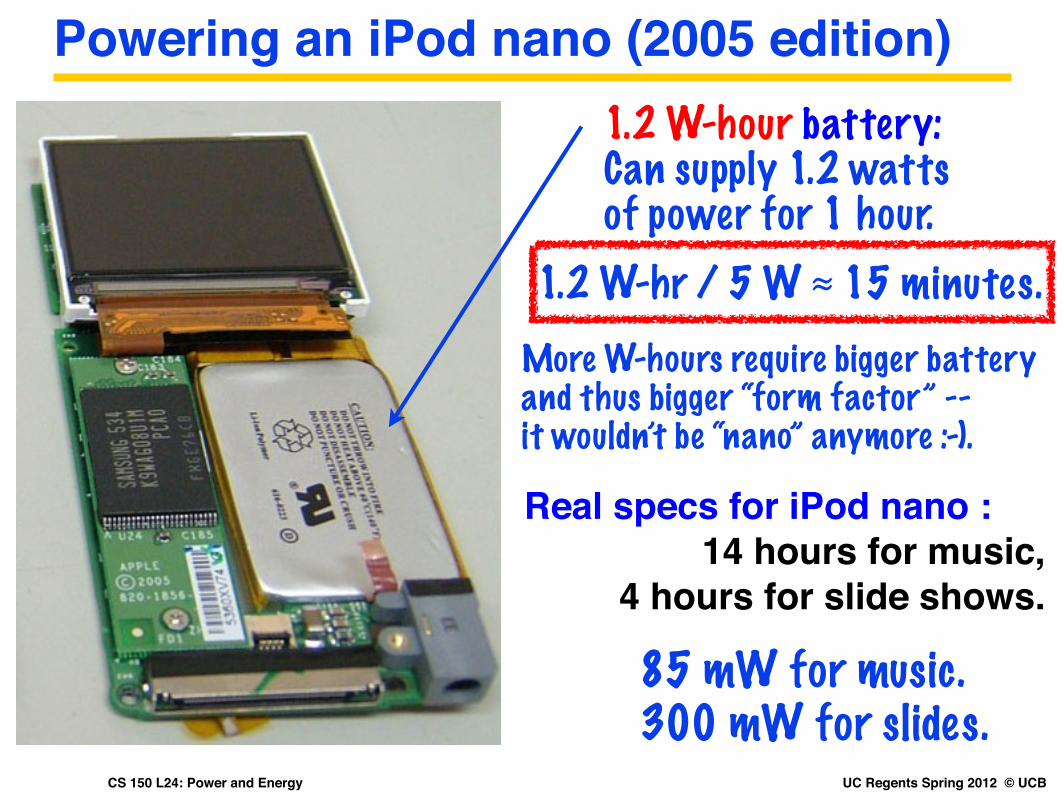
Powering an iPod nano (2005 edition)1.2 W-hour battery: Can supply 1.2 watts of power for 1 hour.
1.2 W-hr / 5 W ≈ 15 minutes.
Real specs for iPod nano : 14 hours for music,
4 hours for slide shows.
85 mW for music.300 mW for slides.
More W-hours require bigger battery and thus bigger “form factor” -- it wouldn’t be “nano” anymore :-).

UC Regents Spring 2012 © UCBEECS 150: Graphics Processors

UC Regents Spring 2012 © UCBCS 150 L24: Power and Energy
Gate delay roughly linear
with Vdd
This magic trick brought to you by Cory Hall ...
3636
Active Power ReductionActive Power Reduction
Slow Fast Slow
Lo
w S
up
ply
Vo
lta
ge
Hig
h S
up
ply
Vo
lta
ge
Multiple Supply
Voltages
Logic BlockFreq = 1
Vdd = 1
Throughput = 1
Power = 1
Area = 1
Pwr Den = 1
Vdd
Logic Block
Freq = 0.5
Vdd = 0.5
Throughput = 1
Power = 0.25
Area = 2
Pwr Den = 0.125
Vdd/2
Logic Block
Replicated DesignsAnd so, we can transform this:
Block processes stereo audio. 1/2 of clocks for “left”, 1/2 for “right”.
P ~ F ⨯ Vdd2
P ~ 1 ⨯ 12
Into this: Top block processes “left”, bottom “right”.
3636
Active Power ReductionActive Power Reduction
Slow Fast Slow
Lo
w S
up
ply
Vo
lta
ge
Hig
h S
up
ply
Vo
lta
ge
Multiple Supply
Voltages
Logic BlockFreq = 1
Vdd = 1
Throughput = 1
Power = 1
Area = 1
Pwr Den = 1
Vdd
Logic Block
Freq = 0.5
Vdd = 0.5
Throughput = 1
Power = 0.25
Area = 2
Pwr Den = 0.125
Vdd/2
Logic Block
Replicated Designs
CV2 power only
P ~ #blks ⨯ F ⨯ Vdd 2
P ~ 2 ⨯ 1/2 ⨯ 1/4 = 1/4
UC Regents Spring 2012 © UCBCS 150 L24: Power and Energy
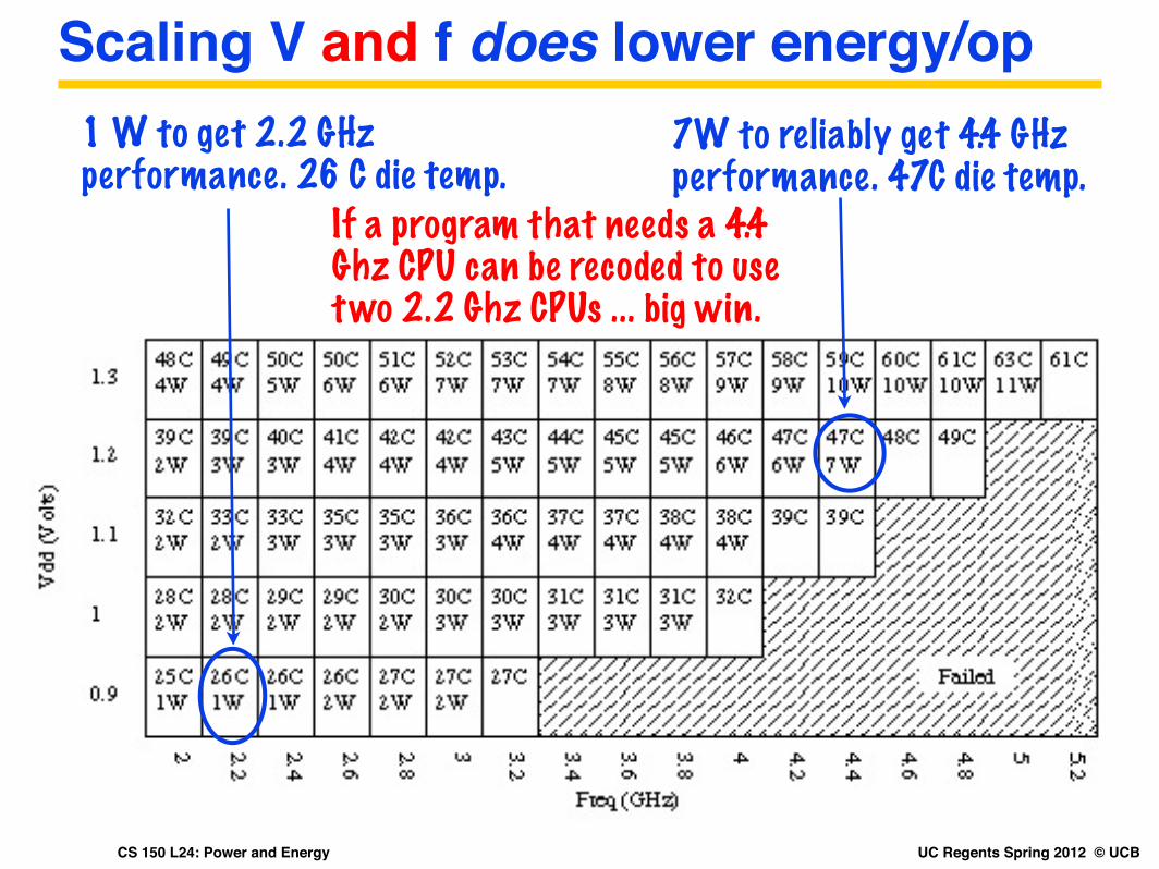
Scaling V and f does lower energy/op7W to reliably get 4.4 GHz performance. 47C die temp.
1 W to get 2.2 GHz performance. 26 C die temp.
If a program that needs a 4.4 Ghz CPU can be recoded to use two 2.2 Ghz CPUs ... big win.
UC Regents Spring 2012 © UCBEECS 150: Graphics Processors
Today: Graphics Processors
Computer Graphics. A brief introduction to “the pipeline”.
Stream Processing. Casting the graphics pipeline into hardware.
Unified Pipelines. GeForce 8800,from Nvidia, introduced in 2006.
Kepler. The latest generation from Nvidia, released last month.
UC Regents Spring 2012 © UCBEECS 150: Graphics Processors
PC Graphics, 2012 Edition
UC Regents Spring 2012 © UCBEECS 150: Graphics Processors
Improved turbo will surely be appreciated. More aggressive turbo bins plus the ability to turbo upabove TDP limits for short periods of time will help make PCs feel more responsive even when doingrelatively benign tasks. Things like launching applications, loading web pages or just opening newwindow stand to benefit.
The architecture sounds a lot like Intel simply did Nehalem/Westmere better. Over time you come upwith newer, better ways to do things and that’s ultimately what Sandy Bridge looks like - a better,more efficient way to do what Conroe, Nehalem and Westmere did before it.
The more dramatic changes happened outside of the cores. GPU performance is clearly an importantSandy Bridge feature as we’ve already shown. I can’t help but be curious about how far Intel couldtake its SNB graphics subsystem if it simply scaled up the number of EUs. The media processingengine, particularly with the video transcode support is very exciting. Assuming image quality ismaintained and there’s good software support at launch, this could very well be Sandy Bridge’s killerfeature. The ability to transcode at over 10x real time on everything from a desktop to a notebook isjust awesome. With good software support, SNB’s video transcode engine could effectively stopconsumer GPU based video encoding in its tracks. The improved video decode engine is also awelcome addition to the Sandy Bridge architecture.
Connecting it all together we have Sandy Bridge’s ring bus. Generally microprocessor designs don’tundergo such a radical changes unless the design will be used for a while to come. The ring bussounds very scalable and should support growth in core count, L3 cache and GPU performance. Thismay end up being the base architecture that takes us from multi-core to many core.
Mobile Sandy Bridge is significantly faster than Arrandale/Clarksfield
Sandy Bridge will ship in Q1 2011 for both notebooks and desktops and from what we’ve heard,pricing will be very compelling. If you're interested in a sneak peak of Sandy Bridge's performance,take a look at our preview here.
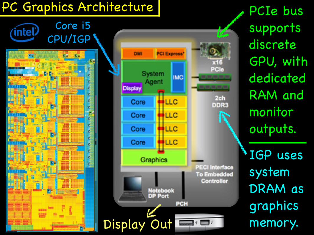
PCIe bus supports discrete GPU, with dedicated RAM and monitor outputs.
IGP uses system DRAM as graphics memory.
PC Graphics ArchitectureCore i5
CPU/IGP
Display Out
UC Regents Spring 2012 © UCBEECS 150: Graphics Processors
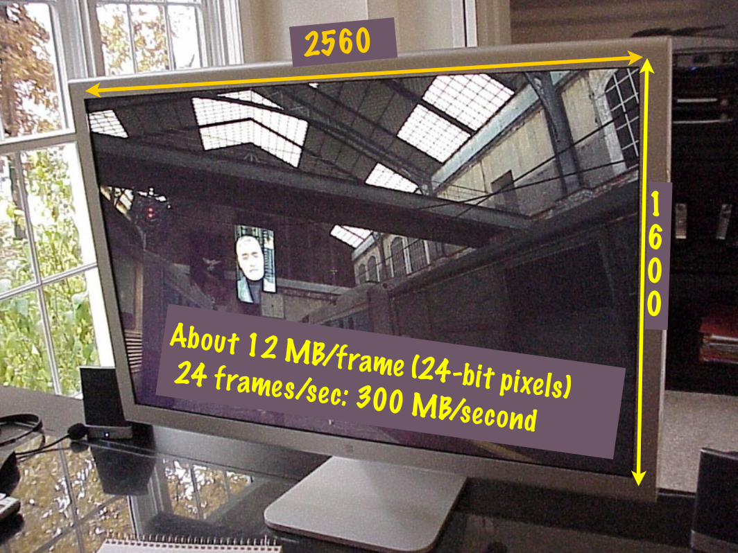
About 12 MB/frame (24-bit pixels)24 frames/sec: 300 MB/second
1600
2560
UC Regents Spring 2012 © UCBEECS 150: Graphics Processors
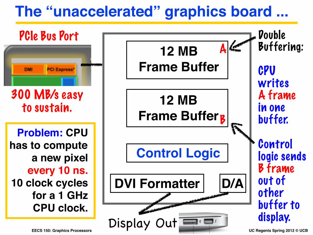
The “unaccelerated” graphics board ...PCIe Bus Port
Problem: CPU has to compute
a new pixel every 10 ns.
10 clock cycles for a 1 GHz CPU clock.
Improved turbo will surely be appreciated. More aggressive turbo bins plus the ability to turbo upabove TDP limits for short periods of time will help make PCs feel more responsive even when doingrelatively benign tasks. Things like launching applications, loading web pages or just opening newwindow stand to benefit.
The architecture sounds a lot like Intel simply did Nehalem/Westmere better. Over time you come upwith newer, better ways to do things and that’s ultimately what Sandy Bridge looks like - a better,more efficient way to do what Conroe, Nehalem and Westmere did before it.
The more dramatic changes happened outside of the cores. GPU performance is clearly an importantSandy Bridge feature as we’ve already shown. I can’t help but be curious about how far Intel couldtake its SNB graphics subsystem if it simply scaled up the number of EUs. The media processingengine, particularly with the video transcode support is very exciting. Assuming image quality ismaintained and there’s good software support at launch, this could very well be Sandy Bridge’s killerfeature. The ability to transcode at over 10x real time on everything from a desktop to a notebook isjust awesome. With good software support, SNB’s video transcode engine could effectively stopconsumer GPU based video encoding in its tracks. The improved video decode engine is also awelcome addition to the Sandy Bridge architecture.
Connecting it all together we have Sandy Bridge’s ring bus. Generally microprocessor designs don’tundergo such a radical changes unless the design will be used for a while to come. The ring bussounds very scalable and should support growth in core count, L3 cache and GPU performance. Thismay end up being the base architecture that takes us from multi-core to many core.
Mobile Sandy Bridge is significantly faster than Arrandale/Clarksfield
Sandy Bridge will ship in Q1 2011 for both notebooks and desktops and from what we’ve heard,pricing will be very compelling. If you're interested in a sneak peak of Sandy Bridge's performance,take a look at our preview here.
300 MB/s easy to sustain.
12 MB Frame Buffer
Double Buffering:
CPU writes A framein one buffer.
A
DVI Formatter D/A
Control Logic
12 MB Frame Buffer
Display Out
Control logic sends B frame out of other buffer to display.
B
UC Regents Spring 2012 © UCBEECS 150: Graphics Processors
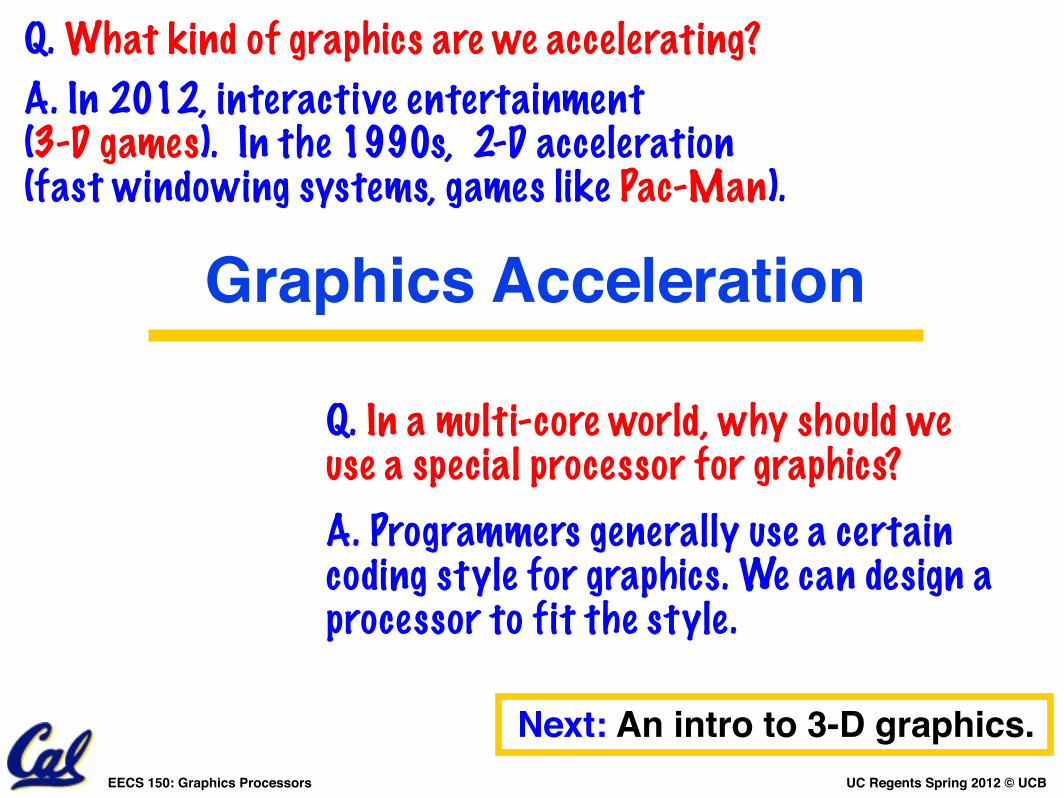
Graphics Acceleration
Q. In a multi-core world, why should we use a special processor for graphics? A. Programmers generally use a certain coding style for graphics. We can design a processor to fit the style.
Q. What kind of graphics are we accelerating?A. In 2012, interactive entertainment (3-D games). In the 1990s, 2-D acceleration (fast windowing systems, games like Pac-Man).
Next: An intro to 3-D graphics.
UC Regents Spring 2012 © UCBEECS 150: Graphics Processors
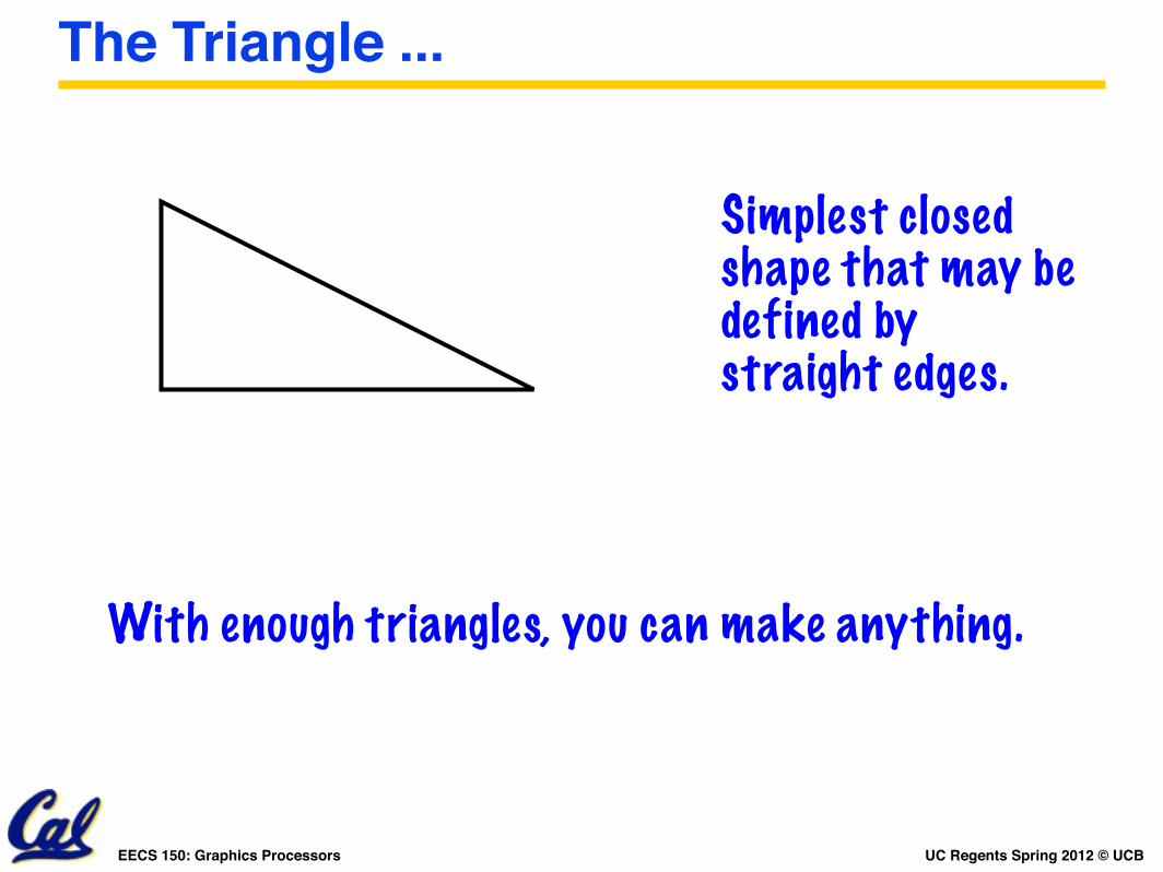
The Triangle ...
Simplest closed shape that may be defined by straight edges.
With enough triangles, you can make anything.

UC Regents Spring 2012 © UCBEECS 150: Graphics Processors
A cube whose faces are made up of triangles. This is a 3-D model of a cube -- model includes faces we can’t see in this view.
A sphere whose faces are made up of triangles. With enough triangles, the curvature of the sphere can be made arbitrarily smooth.
UC Regents Spring 2012 © UCBEECS 150: Graphics Processors
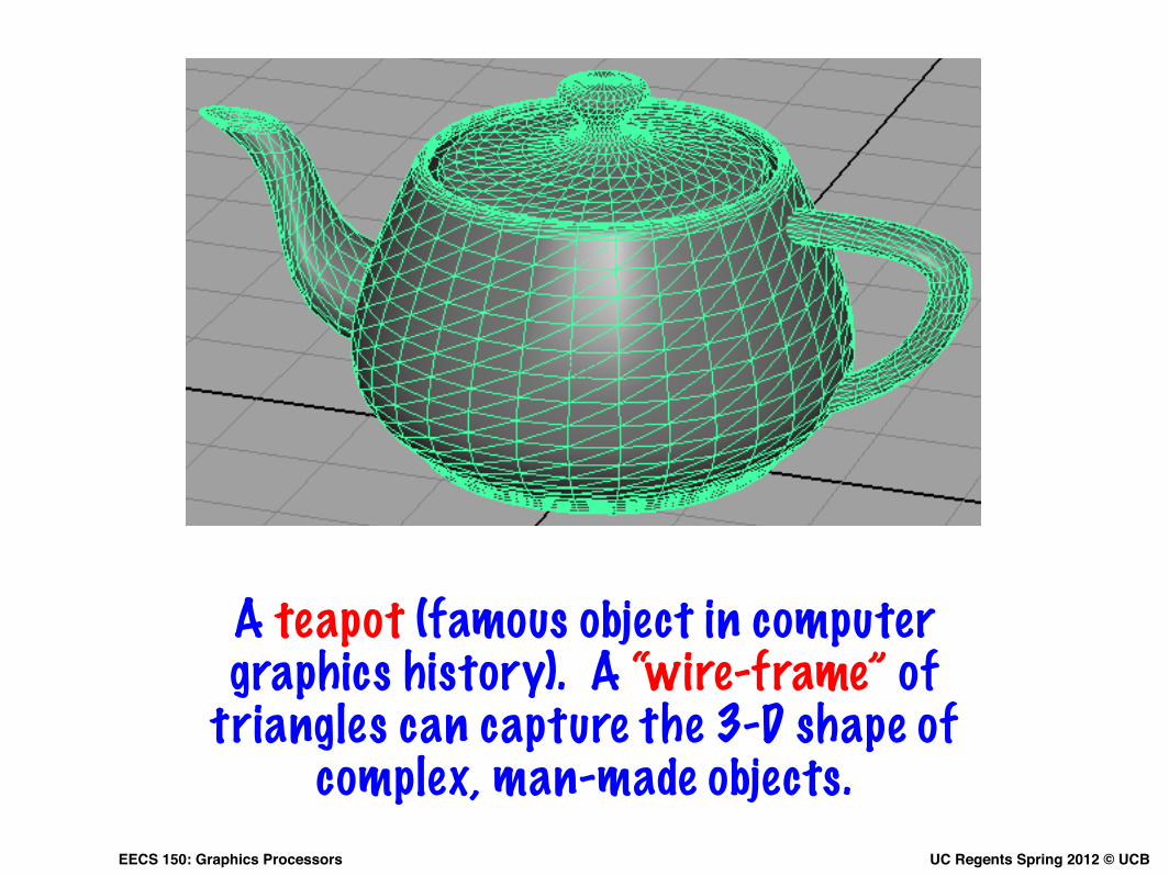
A teapot (famous object in computer graphics history). A “wire-frame” of
triangles can capture the 3-D shape of complex, man-made objects.
UC Regents Spring 2012 © UCBEECS 150: Graphics Processors
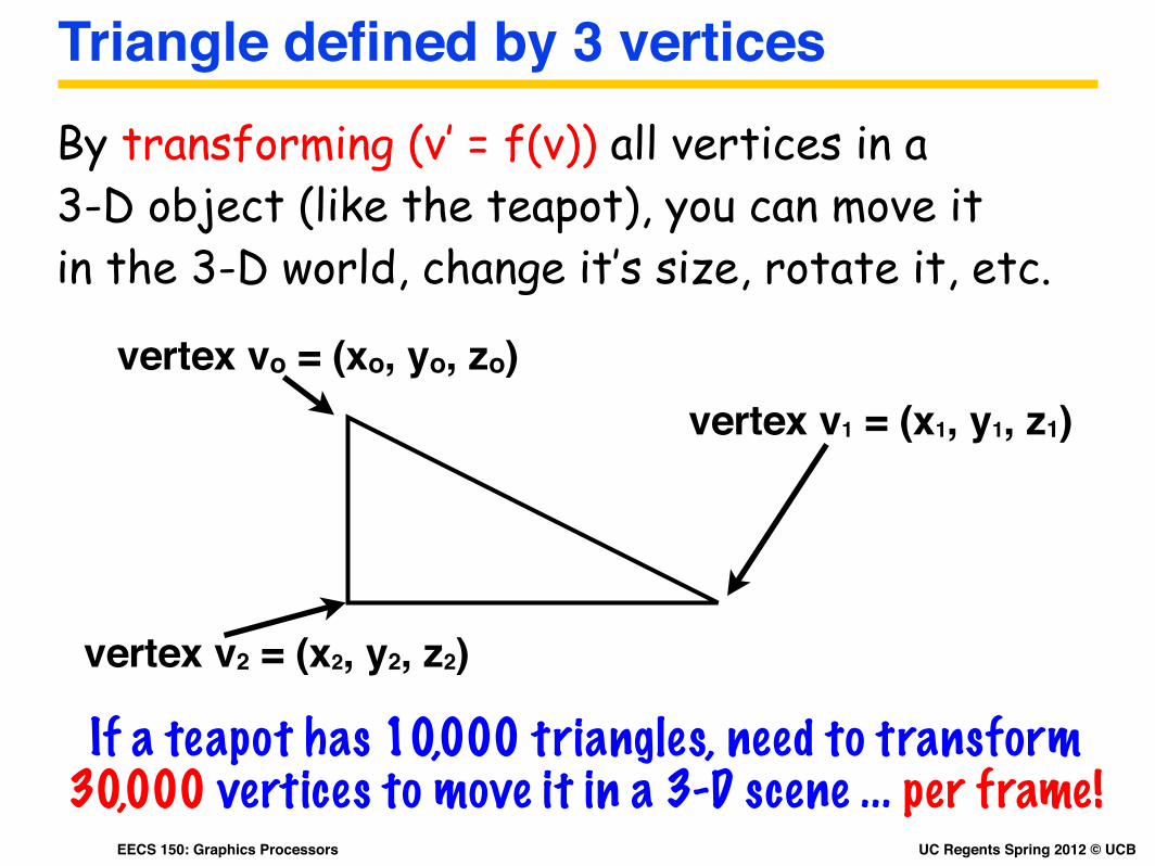
Triangle defined by 3 verticesBy transforming (v’ = f(v)) all vertices in a 3-D object (like the teapot), you can move it in the 3-D world, change it’s size, rotate it, etc.
vertex vo = (xo, yo, zo)vertex v1 = (x1, y1, z1)
vertex v2 = (x2, y2, z2)
If a teapot has 10,000 triangles, need to transform 30,000 vertices to move it in a 3-D scene ... per frame!
UC Regents Spring 2012 © UCBEECS 150: Graphics Processors
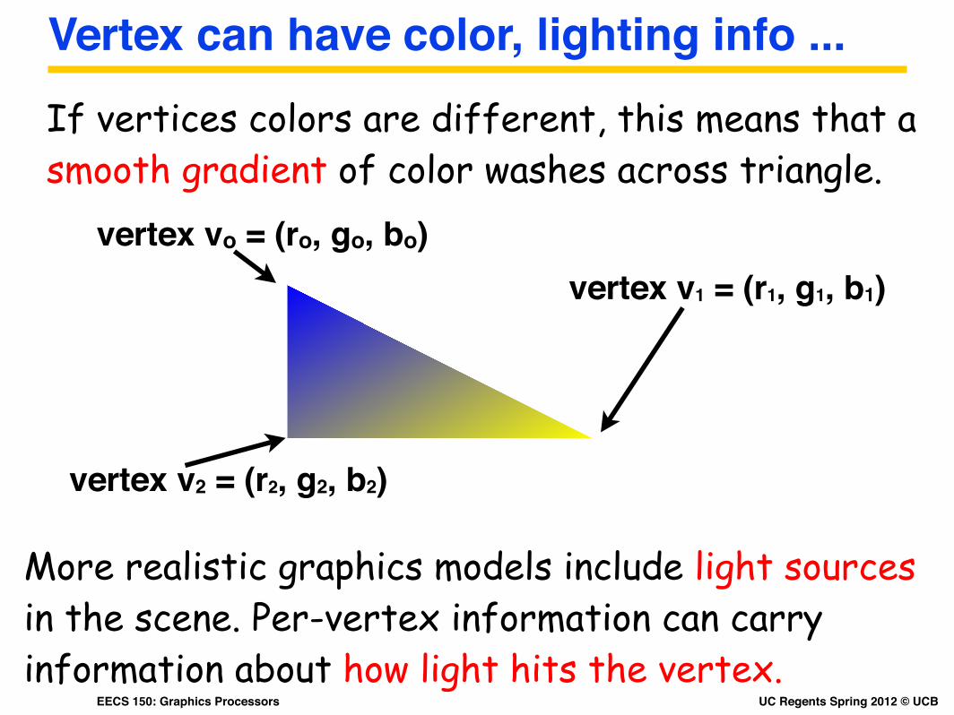
Vertex can have color, lighting info ...If vertices colors are different, this means that a smooth gradient of color washes across triangle.
vertex vo = (ro, go, bo)vertex v1 = (r1, g1, b1)
vertex v2 = (r2, g2, b2)
More realistic graphics models include light sources in the scene. Per-vertex information can carry information about how light hits the vertex.
UC Regents Spring 2012 © UCBEECS 150: Graphics Processors
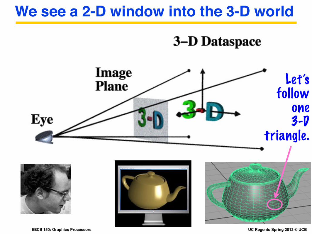
We see a 2-D window into the 3-D world
Let’s follow
one 3-D
triangle.
UC Regents Spring 2012 © UCBEECS 150: Graphics Processors
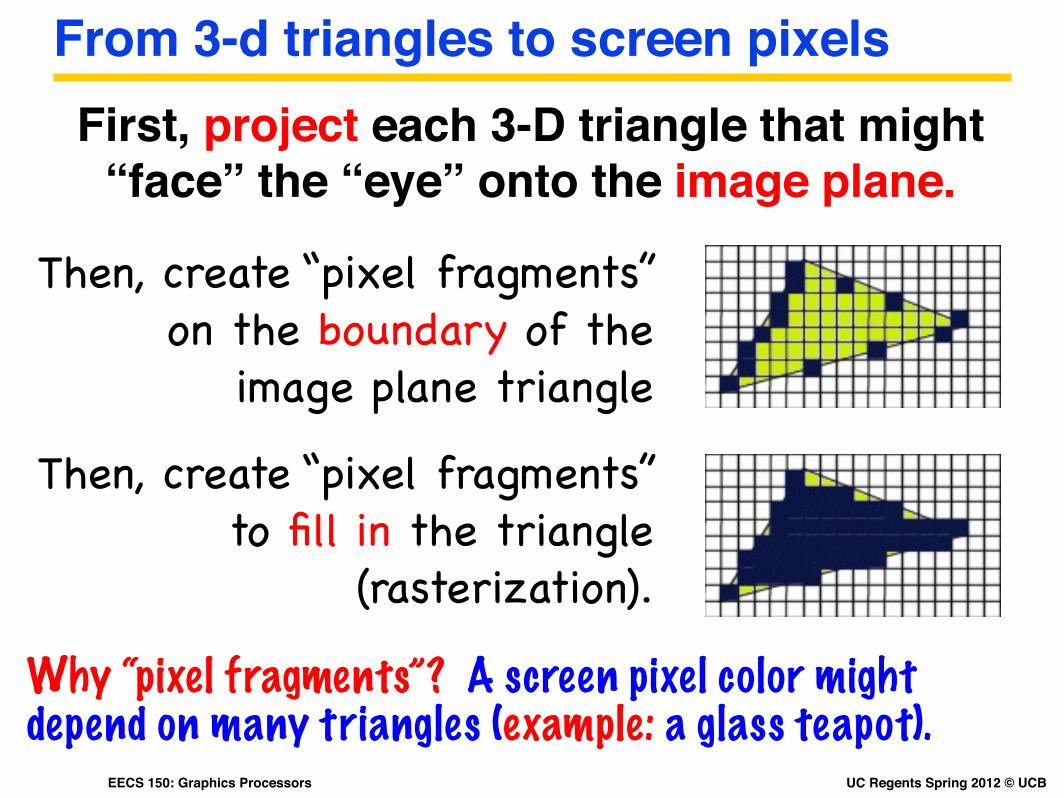
From 3-d triangles to screen pixelsFirst, project each 3-D triangle that might
“face” the “eye” onto the image plane.
Then, create “pixel fragments” on the boundary of the
image plane triangle
Then, create “pixel fragments” to fill in the triangle
(rasterization).
Why “pixel fragments”? A screen pixel color might depend on many triangles (example: a glass teapot).
UC Regents Spring 2012 © UCBEECS 150: Graphics Processors
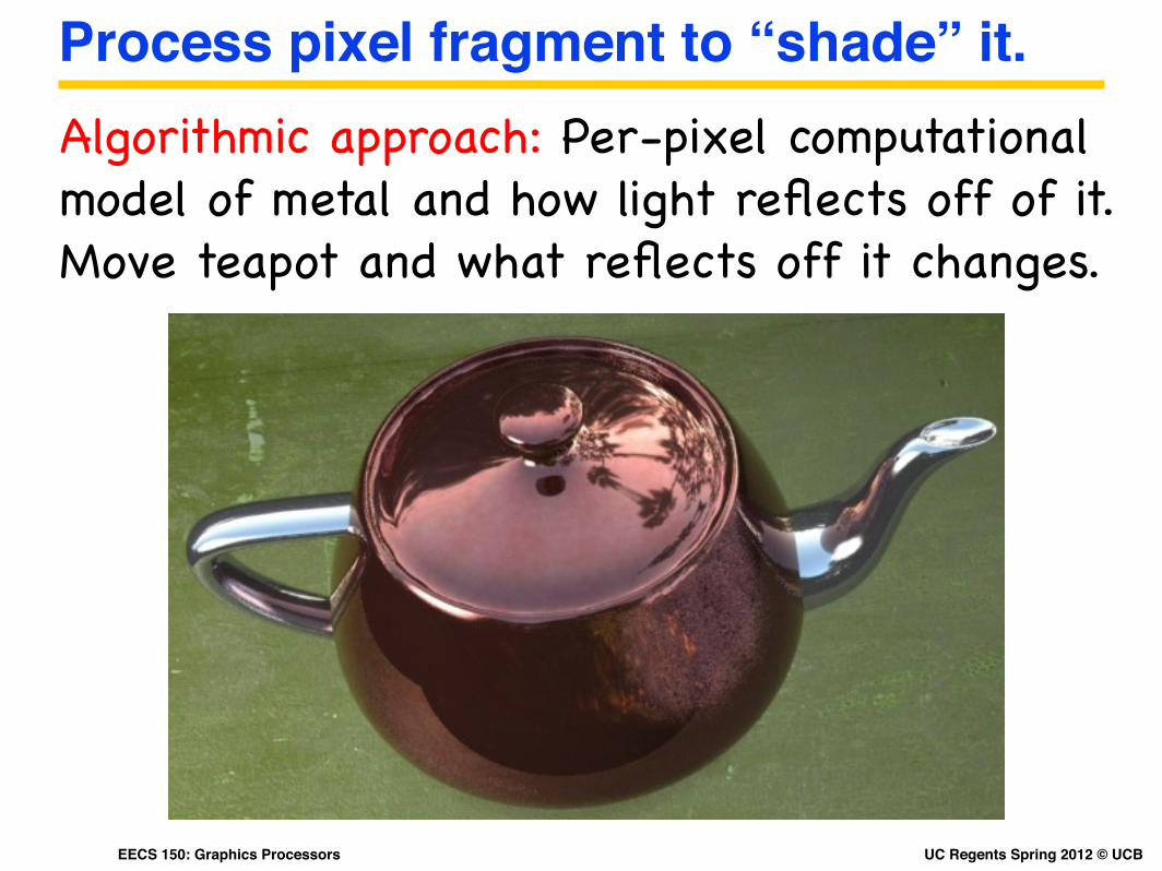
Process pixel fragment to “shade” it.Algorithmic approach: Per-pixel computational model of metal and how light reflects off of it. Move teapot and what reflects off it changes.
UC Regents Spring 2012 © UCBEECS 150: Graphics Processors
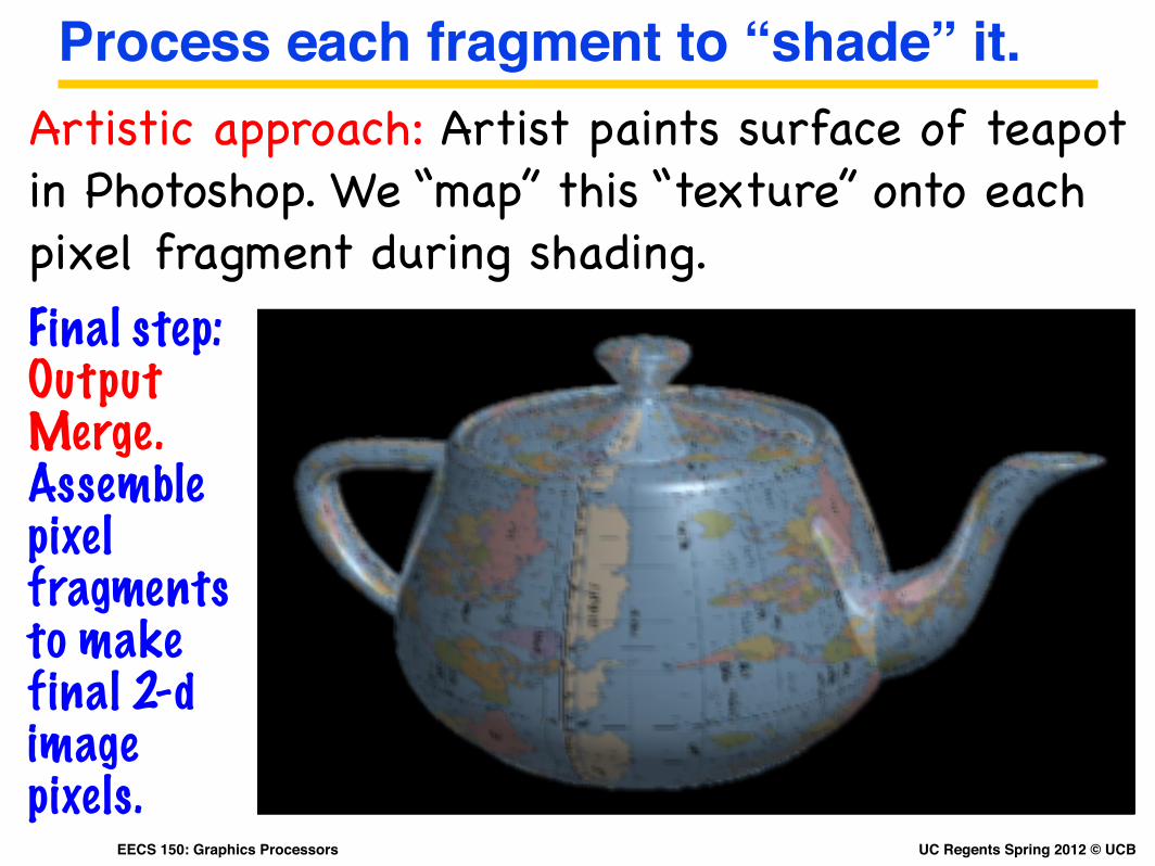
Process each fragment to “shade” it.Artistic approach: Artist paints surface of teapot in Photoshop. We “map” this “texture” onto each pixel fragment during shading.Final step: Output Merge. Assemble pixel fragments to make final 2-d image pixels.
UC Regents Spring 2012 © UCBEECS 150: Graphics Processors
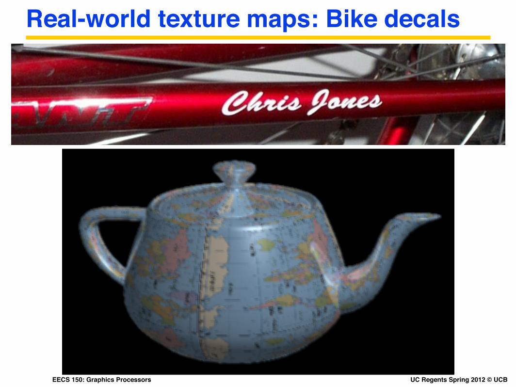
Real-world texture maps: Bike decals
UC Regents Spring 2012 © UCBEECS 150: Graphics Processors
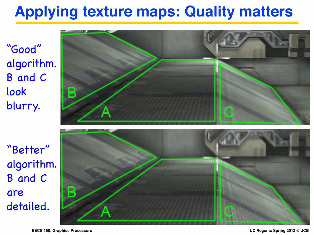
Applying texture maps: Quality matters
“Good” algorithm. B and C look blurry.
“Better” algorithm. B and C aredetailed.
UC Regents Spring 2012 © UCBEECS 150: Graphics Processors
Putting it All Together ...
Luxo, Jr: Short movie made by Pixar, shown at SIGGRAPH in 1986.
First Academy Award given to a computer graphics movie.

UC Regents Spring 2012 © UCBEECS 150: Graphics Processors
UC Regents Spring 2012 © UCBEECS 150: Graphics Processors
Graphics Acceleration
Next: Back to architecture ...

UC Regents Spring 2012 © UCBEECS 150: Graphics Processors
The graphics pipeline in hardware (2004)Figure 2-1 Block diagram
167 MHzMaxBus
12 MbpsUSB
PCI bus
BootROM
USB 2.0 port (480 Mbps)
USB 2.0 port (480 Mbps)
PCI USB 2.0controller
DDR SDRAMDIMM slot
32 MBDDR RAM
DVI/VGA/composite/S-videooutput port
Ethernet port10/100 Mbps
FireWire 400 port
AGP 4Xbus
167 MHzMemory
bus
PMUpower controller
Powerbutton Fan
Opticaldrive
UltraATA/100
bus
Device 0
Device 1
Headphone/audio line-out jack
Hard diskdrive
Radeon9200
graphics IC
Audiocodec
EthernetPHY
FireWirePHY
PowerPC G4microprocessor
(L2 cache: 512K 1:1)
AirPort Extreme
I2S
I2S
I2C
BluetoothModem port
Modem module
Data pumpand DAA
Built-inspeaker
Intrepidmemorycontrollerand I/Odevice
controller
Main ICs and Buses
The architecture of Mac mini is designed around the PowerPC G4 microprocessor and the Intrepidmemory and I/O device controller. The Intrepid occupies the center of the block diagram.
The MaxBus connects the PowerPC G4 microprocessor to the Intrepid ASIC. The MaxBus has 64 datalines, 32 address lines, and a bus clock speed of 167 MHz. The Intrepid ASIC has other buses thatconnect with the boot ROM, the hard disk drive, and the optical drive, the power controller IC, thesound IC, the internal modem module, and the optional wireless LAN module.
The Intrepid I/O controller has a 32-bit PCI bus with a bus clock speed of 33 MHz.
Each of the components listed here is described in one of the following sections.
16 Block Diagram and Buses2005-04-05 | © 2005 Apple Computer, Inc. All Rights Reserved.
C H A P T E R 2
Architecture
Output Merge
Figure 2-1 Block diagram
167 MHzMaxBus
12 MbpsUSB
PCI bus
BootROM
USB 2.0 port (480 Mbps)
USB 2.0 port (480 Mbps)
PCI USB 2.0controller
DDR SDRAMDIMM slot
32 MBDDR RAM
DVI/VGA/composite/S-videooutput port
Ethernet port10/100 Mbps
FireWire 400 port
AGP 4Xbus
167 MHzMemory
bus
PMUpower controller
Powerbutton Fan
Opticaldrive
UltraATA/100
bus
Device 0
Device 1
Headphone/audio line-out jack
Hard diskdrive
Radeon9200
graphics IC
Audiocodec
EthernetPHY
FireWirePHY
PowerPC G4microprocessor
(L2 cache: 512K 1:1)
AirPort Extreme
I2S
I2S
I2C
BluetoothModem port
Modem module
Data pumpand DAA
Built-inspeaker
Intrepidmemorycontrollerand I/Odevice
controller
Main ICs and Buses
The architecture of Mac mini is designed around the PowerPC G4 microprocessor and the Intrepidmemory and I/O device controller. The Intrepid occupies the center of the block diagram.
The MaxBus connects the PowerPC G4 microprocessor to the Intrepid ASIC. The MaxBus has 64 datalines, 32 address lines, and a bus clock speed of 167 MHz. The Intrepid ASIC has other buses thatconnect with the boot ROM, the hard disk drive, and the optical drive, the power controller IC, thesound IC, the internal modem module, and the optional wireless LAN module.
The Intrepid I/O controller has a 32-bit PCI bus with a bus clock speed of 33 MHz.
Each of the components listed here is described in one of the following sections.
16 Block Diagram and Buses2005-04-05 | © 2005 Apple Computer, Inc. All Rights Reserved.
C H A P T E R 2
Architecture
To display
Create pixels fragments
Algorithms are usually hardwired
Process each vertex
3-D vertex “stream” sent by CPU
Programmable CPU”Vertex Shader”
Process pixel fragments
Programmable CPU”Pixel Shader”
Programming Language/API? DirectX, OpenGL
UC Regents Spring 2012 © UCBEECS 150: Graphics Processors
Vertex Shader: A “stream processor”
Shader CPU
Input Registers (Read Only)
Vertex “stream” from CPUOnly one vertex at a time placed in input registers.
Constant Registers
(Read Only)
From CPU: changes slowly (per frame,
per object)
Output Registers (Write Only)
Vertex “stream” ready for 3-D to 2-D conversion
Shader creates one vertex out for each vertex in.Working
Registers (Read/Write)
Shader Program Memory
Short (ex: 128 instr)straight-line code. Same code runs on every vertex.

UC Regents Spring 2012 © UCBEECS 150: Graphics Processors
Optimized instructions and data formats
Input Registers
From CPU
Output Registers
Shader CPU Shader Program Memory
128-bit registers, holding four 32-bit floats.
Typical use: (x,y,z,w) representation of a point in 3-Dspace.
x y z w
x y z w
Typical instruction:
rsq dest src
dest.{x,y,z,w} = 1.0/sqrt(abs(src.w)).If src.w=0, dest ∞.
The 1/sqrt() function is often used in graphics.
To 3-D/2-D
UC Regents Spring 2012 © UCBEECS 150: Graphics Processors
Easy to parallelize: Vertices independent
Input Registers
From CPU
Output Registers
Shader CPU
x y z w
x y z w
Input Registers
Output Registers
Shader CPU
x y z w
x y z w
To 3-D/ 2-D
Caveat: Care might be needed when merging streams.
Why?3-D to 2-D may expect triangle vertices in order in the stream.
Shader CPUs easy to multithread.
UC Regents Spring 2012 © UCBEECS 150: Graphics Processors
Pixel shader specializations ...
Process each vertex
Create pixels fragments
Output Merge
Figure 2-1 Block diagram
167 MHzMaxBus
12 MbpsUSB
PCI bus
BootROM
USB 2.0 port (480 Mbps)
USB 2.0 port (480 Mbps)
PCI USB 2.0controller
DDR SDRAMDIMM slot
32 MBDDR RAM
DVI/VGA/composite/S-videooutput port
Ethernet port10/100 Mbps
FireWire 400 port
AGP 4Xbus
167 MHzMemory
bus
PMUpower controller
Powerbutton Fan
Opticaldrive
UltraATA/100
bus
Device 0
Device 1
Headphone/audio line-out jack
Hard diskdrive
Radeon9200
graphics IC
Audiocodec
EthernetPHY
FireWirePHY
PowerPC G4microprocessor
(L2 cache: 512K 1:1)
AirPort Extreme
I2S
I2S
I2C
BluetoothModem port
Modem module
Data pumpand DAA
Built-inspeaker
Intrepidmemorycontrollerand I/Odevice
controller
Main ICs and Buses
The architecture of Mac mini is designed around the PowerPC G4 microprocessor and the Intrepidmemory and I/O device controller. The Intrepid occupies the center of the block diagram.
The MaxBus connects the PowerPC G4 microprocessor to the Intrepid ASIC. The MaxBus has 64 datalines, 32 address lines, and a bus clock speed of 167 MHz. The Intrepid ASIC has other buses thatconnect with the boot ROM, the hard disk drive, and the optical drive, the power controller IC, thesound IC, the internal modem module, and the optional wireless LAN module.
The Intrepid I/O controller has a 32-bit PCI bus with a bus clock speed of 33 MHz.
Each of the components listed here is described in one of the following sections.
16 Block Diagram and Buses2005-04-05 | © 2005 Apple Computer, Inc. All Rights Reserved.
C H A P T E R 2
Architecture
Pixel shader needs fast access to the map of Europe on teapot (via graphics card RAM).
Texture maps (look-up tables) play a key role.
Process pixel fragments
”Pixel Shader” CPU
UC Regents Spring 2012 © UCBEECS 150: Graphics Processors
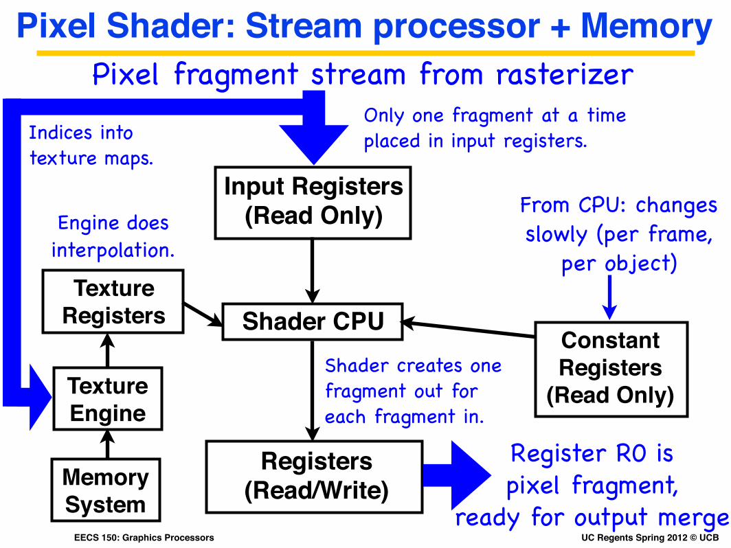
Pixel Shader: Stream processor + Memory
Shader CPU
Input Registers (Read Only)
Pixel fragment stream from rasterizerOnly one fragment at a time placed in input registers.
Constant Registers
(Read Only)
From CPU: changes slowly (per frame,
per object)
Registers (Read/Write)
Register R0 is pixel fragment,
ready for output merge
Shader creates one fragment out for each fragment in.
Indices into texture maps.
TextureRegisters
Texture Engine
Memory System
Engine does interpolation.
UC Regents Spring 2012 © UCBEECS 150: Graphics Processors
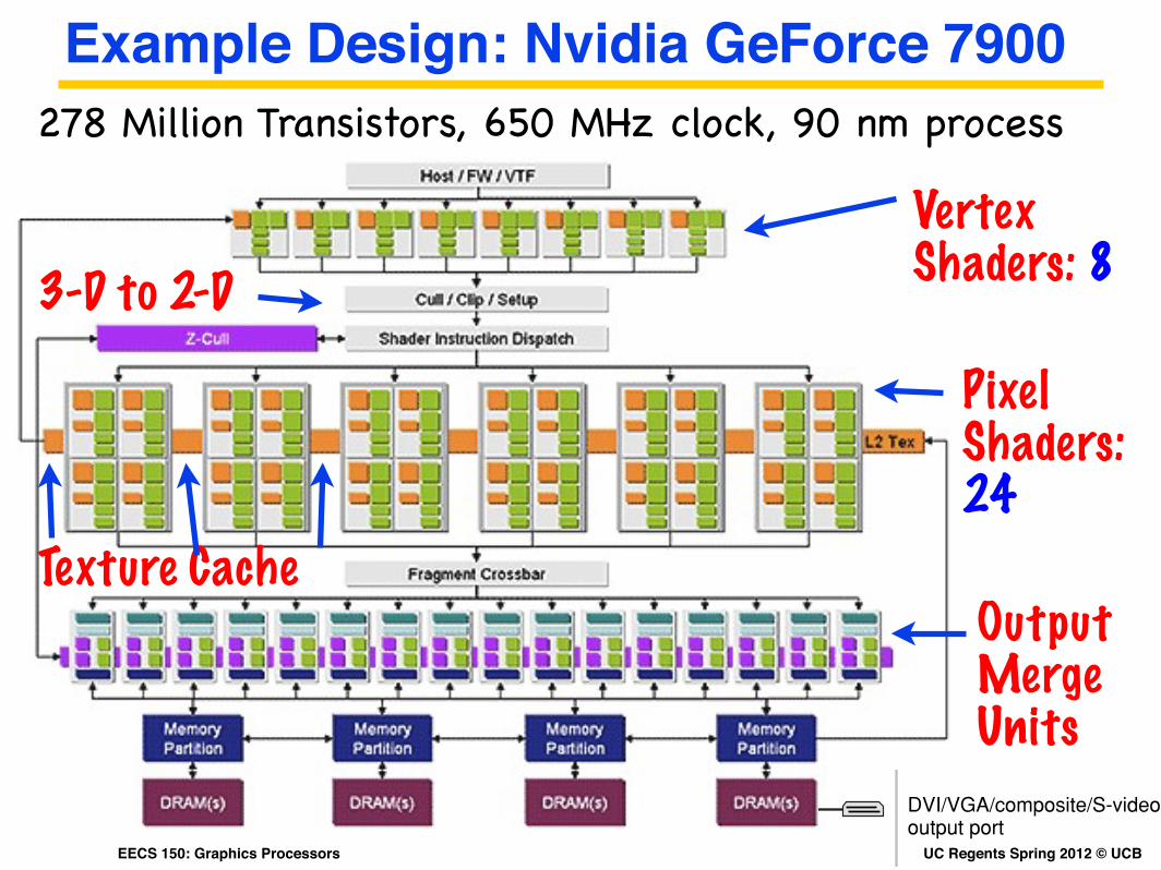
Example Design: Nvidia GeForce 7900
Vertex Shaders: 8
Pixel Shaders:24
3-D to 2-D
Output Merge Units
Texture Cache
278 Million Transistors, 650 MHz clock, 90 nm process
Figure 2-1 Block diagram
167 MHzMaxBus
12 MbpsUSB
PCI bus
BootROM
USB 2.0 port (480 Mbps)
USB 2.0 port (480 Mbps)
PCI USB 2.0controller
DDR SDRAMDIMM slot
32 MBDDR RAM
DVI/VGA/composite/S-videooutput port
Ethernet port10/100 Mbps
FireWire 400 port
AGP 4Xbus
167 MHzMemory
bus
PMUpower controller
Powerbutton Fan
Opticaldrive
UltraATA/100
bus
Device 0
Device 1
Headphone/audio line-out jack
Hard diskdrive
Radeon9200
graphics IC
Audiocodec
EthernetPHY
FireWirePHY
PowerPC G4microprocessor
(L2 cache: 512K 1:1)
AirPort Extreme
I2S
I2S
I2C
BluetoothModem port
Modem module
Data pumpand DAA
Built-inspeaker
Intrepidmemorycontrollerand I/Odevice
controller
Main ICs and Buses
The architecture of Mac mini is designed around the PowerPC G4 microprocessor and the Intrepidmemory and I/O device controller. The Intrepid occupies the center of the block diagram.
The MaxBus connects the PowerPC G4 microprocessor to the Intrepid ASIC. The MaxBus has 64 datalines, 32 address lines, and a bus clock speed of 167 MHz. The Intrepid ASIC has other buses thatconnect with the boot ROM, the hard disk drive, and the optical drive, the power controller IC, thesound IC, the internal modem module, and the optional wireless LAN module.
The Intrepid I/O controller has a 32-bit PCI bus with a bus clock speed of 33 MHz.
Each of the components listed here is described in one of the following sections.
16 Block Diagram and Buses2005-04-05 | © 2005 Apple Computer, Inc. All Rights Reserved.
C H A P T E R 2
Architecture
UC Regents Spring 2012 © UCBEECS 150: Graphics Processors
Break Time ...
Next: Unified architectures
Play
UC Regents Spring 2012 © UCBEECS 150: Graphics Processors
Unified Architectures
Basic idea: Replace specialized logic (vertex shader, pixel shader, hardwired algorithms) with many copies of one unified CPU design.
Consequence: You no longer “see” the graphics pipeline when you look at the architecture block diagram.
Designed for: DirectX 10 (Microsoft Vista), and new non-graphics markets for GPUs.
UC Regents Spring 2012 © UCBEECS 150: Graphics Processors
throughput by exploiting the natural independence between verti-ces and between pixels fragments. Multiple instances of vertex and pixel shaders are used to process independent vertices and pixel fragments in parallel. Hardware implementations typically include a larger number of pixel shaders than vertex shaders re-flecting the higher ratio of pixels to vertices in a typical rendering workload [Montrym and Moreton 2005]. This characteristic also influences the cost of pixel shaders relative to vertex shaders since pixel shaders are more heavily replicated.
The programmable pipeline is directed using a low-level ab-straction layer such as OpenGL or Direct3D. The abstraction layer serves to hide the differences between varying implementa-tions of the pipeline and provide a more convenient programming abstraction. Fixed platforms, such as consoles, differ from PCs in that there is only one hardware implementation, so often low-level details of the hardware are exposed through the abstraction layer.
We refer to the abstraction layer as a runtime and it is con-trolled through its API. The runtime provides device independent resource management (allocation, lifetime, initialization, virtual-ization, etc) for texture maps, vertex buffers, and other state and it communicates with the hardware accelerator through device-dependent driver software. The transition to a programmable pipeline has added the task of abstracting and managing shader programs to the runtime.
The limited instruction store of early programmable proces-sors made the choice of programming in an assembly-like lan-guage [Gray 2003] both practical and in many cases necessary to maximize control of the limited resources. However, modest increases in available hardware resources created a need for a higher-level programming abstraction to maximize programmer productivity. C-like programming languages with some customi-zations to match the underlying rendering pipeline (4-vectors, intrinsics, I/O registers) answered this need [Proudfoot et al. 2001; Microsoft 2002; Mark 2003; Kessenich 2004; McCool and Du Toit 2004;] Additionally, other languages have been developed to explore the use of the substantial floating-point processing and memory bandwidth of GPUs for application domains other than
rendering [Buck et al. 2004; McCormick et al. 2004], but we will not address this latter subject further in this paper.
While there are similarities to imperative CPU programming languages (notably C), there are some significant departures. For example, the machine and compilation model is more virtual ma-chine-like, with the shader assembly language serving as a ma-chine-independent intermediate language (IL) rather than a spe-cific machine language1. Though a high-level language like Mi-crosoft’s HLSL can be compiled to IL offline, the translation to the target hardware occurs just in time (JIT) at run-time with the translator implemented as part of the driver infrastructure for the GPU. We note that the OpenGL Shading Language takes a dif-ferent approach with the entire compilation process occuring at run-time.
Another significant difference is that shading programs are not standalone applications, and are instead executing in concert with a program executing on the CPU that orchestrates the render-ing pipeline. The CPU program also supplies parameters to the shading program in the form of texture maps or by populating on-chip registers called constants.
While this paper does not describe a specific hardware em-bodiment of the new pipeline architecture, the pipeline design is shaped significantly by hardware practicalities and was designed concurrently with multiple hardware implementations. Many of the structural underpinnings from current hardware implementa-tions [ATI 2005; Doggett 2005; Montrym and Moreton 2005] continue to be both relevant and influential in this design.
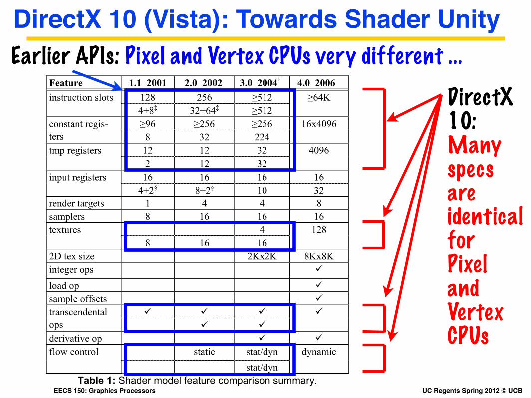
Feature 1.1 2001 2.0 2002 3.0 2004† 4.0 2006
128 256 !512 instruction slots
4+8‡ 32+64‡!512
!64K
!96 !256 !256 constant regis-
ters 8 32 224
16x4096
12 12 32 tmp registers
2 12 32
4096
16 16 16 16 input registers
4+2§ 8+2§ 10 32
render targets 1 4 4 8
samplers 8 16 16 16
4 textures
8 16 16
128
2D tex size 2Kx2K 8Kx8K
integer ops !
load op !
sample offsets !
! ! ! transcendental
ops ! !
!
derivative op ! !
static stat/dyn flow control
stat/dyn
dynamic
Table 1: Shader model feature comparison summary. 5specification released in 2002, hardware in 2004;
<texture load > arithmetic
instructions; ?texture > color registers; dashed line separates vertex shader
(above) from pixel shader (below)
3. The Pipeline
The Direct3D 10 pipeline retains the structure of the traditional hardware-accelerated 3D pipeline. Two new stages have been added and other stages have been either simplified or further gen-eralized. The basic pipeline is illustrated in Figure 1. For consis-tency we describe each of the pipeline stages, rather than just the additions. We use traditional terms such as vertex, texture, and pixel for continuity with prior nomenclature, but acknowledge that this terminology reflects a specific usage of a more general processing capability.
Input Assembler (IA) gathers 1D vertex data from up to 8 input streams attached to vertex buffers and converts data items to a canonical format (e.g., float32). Each stream specifies an inde-pendent vertex structure containing up to 16 fields (called ele-ments). An element is a homogenous tuple of 1 to 4 data items (e.g., float32s). A vertex is assembled by reading from the cur-rently enabled streams. Normally vertex data is read sequentially from each vertex buffer; however, if an index buffer is specified then each stream uses a shared index to compute the offset into each vertex buffer. Indexing allows additional performance op-timizations in that the vertex processor computes a result that is completely determined by the index value, therefore recomputa-tion of results for the same index can be avoided using a result cache indexed by the index value.
The IA also supports a mechanism that allows the IA to effec-tively replicate an object n times. This mechanism is an address-ing mode referred to as instancing in which a repeat count n is associated with block of k vertices (corresponding to an object). At the same time, the primitive data is “tagged” with a current instance, primitive, and vertex id and these ids can be accessed in the programmable stages to compute values such as transforma-tions or material parameters based on these ids.
1 This does contradict the notion that the assembly-level shader program-
mer has absolute control.
DirectX 10 (Vista): Towards Shader UnityEarlier APIs: Pixel and Vertex CPUs very different ...
DirectX 10: Many specs are identical for Pixel and Vertex CPUs
UC Regents Spring 2012 © UCBEECS 150: Graphics Processors
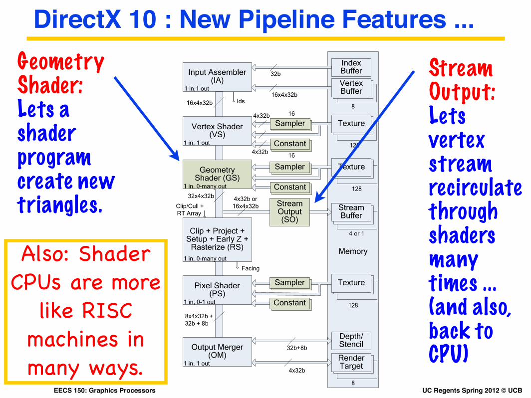
DirectX 10 : New Pipeline Features ...
Vertex Shader (VS) is most commonly used to transform vertices from object space to clip space. The VS reads a single vertex and produces a single vertex as output. The VS and other programmable stages share a common feature set that includes an expanded set of floating-point, integer, control, and memory read instructions allowing access to up to 128 memory buffers (tex-tures) and 16 parameter (constant) buffers. This common core is described in more detail in Section 4.
Geometry Shader (GS) takes the vertices of a single primi-tive (point, line segment, or triangle) as input and generates the vertices of zero or more primitives. The input and output primi-tive types need not match, but they are fixed for the shader pro-gram. A GS program can amplify the number of input primitives by emitting additional primitives subject to a per-invocation limit of 1024 32-bit values of vertex data. Triangles and lines are out-put as connected strips of vertices. A GS program can output more than one strip in a single invocation or it can effectively delete an input primitive by not producing an output. A GS pro-gram can also simply affix additional attributes to a primitive without generating additional geometry, for example, computing additional uniform-valued attributes for each primitive. Since all of the primitive vertices are available, geometric attributes such as a triangle’s plane equation can be readily computed.
In addition to the traditional input primitives, triangle and line primitives may also be processed with their adjacent vertices. A triangle comprises 3 vertices plus 3 adjacent vertices while a line has 2 vertices with 2 adjacent vertices as shown in Figure 2. Ad-jacent vertices are included as part of the vertex buffer formats for triangle and line primitives and are extracted by the IA when a primitive topology with adjacency is specified (rendered).
Stream Output (SO) copies a subset of the vertex informa-tion output by the GS to up to 4 1D output buffers in sequential
order. Ideally the SO should have symmetric output capabilities with the (non-indexed) input capabilities of the IA (8 streams x 16 elements), but the hardware costs were not justified. The SO is limited to either 1 multi-element output stream of up to 16 ele-ments or up to 4 single-element output streams. While the IA can support reading from 8- and 16-bit data types and converting to float32, the SO can only write raw 32-bit data types. However, data conversion and packing can be easily implemented in a GS program reducing the need for fixed-function support.
Set-up and Rasterization Stage (RS) is a fixed-function stage handling clipping, culling, perspective divide, viewport transform, primitive set-up, scissoring, depth offset, and fragment generation. Modern GPU designs invariably include some form of early depth processing (z-cull, hierarchical-z) [ATI 2005; Mon-trym and Moreton 2005] as well. We explicitly mention this op-timization as it is becoming less transparent to application devel-opers. The input of the RS is the vertices and attributes of a single primitive and the output is a series of pixel fragments.
The pixel shader program specifies the manner in which ver-tex attributes are interpolated to produce fragment attributes (no interpolation, non-perspective-corrected interpolation, or perspec-tive-corrected interpolation). Modern GPUs usually support mul-tisample antialiasing [Akeley 1993]. Multisampling requires additional care in specifying attribute evaluation behavior when a fragment does not include the pixel center, since center evaluation may result in an out-of-gamut value. An additional evaluation qualifier (centroid) can be specified to request evaluation within the fragment boundaries.
Pixel Shader (PS) reads the attributes of a single pixel frag-ment and produces a single output fragment consisting of 1 to 8 attribute (color) values and optionally a depth value. The attrib-ute values (elements) are each written to a separate color buffer (termed a render target) or the entire result may be discarded (no fragment is output). Normally depth and stencil values are for-warded from the RS. However, the PS can replace the depth value with a computed value, but not the stencil value. Both dis-carding pixels and replacing the depth value may defeat depth-processing optimizations in the RS since they can change the fragment’s visibility.
Figure 1: Direct3D 10 pipeline.
/a1or additions are highlighted.
!"#$%&'(()*+,)-.!'/
012),&3456)-.03/
7$%#$%&8)-9)-.78/
:,1#&;&0-<=)>%&;3)%$#&;&?5-,@&A&;&
B5(%)-1C)&.B3/
D)-%)2&3456)-.D3/
E)<*)%-@&3456)-&.E3/
8)*<-@
!"6)2F$GG)-
H)#%4I3%)">1,
3%-)5*7$%#$%&.37/
J2KL+
J2KL+
KL+
MN2J2KL+
KL+;O+
J2KL+&<-
MN2J2KL+
D)-%)2F$GG)-
D)-%)2F$GG)-
P)2%$-)
O
MLO
P)2%$-)
3%-)5*F$GG)-
P)2%$-)
B)"6)-P5-9)%
J&<-&M
MLO
O
35*#,)-
MN
35*#,)-
35*#,)-
MN
MN2J2KL+
KL2J2KL+
&&&O2J2KL+&;
KL+&;&O+
!6(
&:,1#I:$,,&;&
BP&'--5@
:<"(%5"%
:<"(%5"%
:<"(%5"%
J2KL+
Q5>1"9
MLO
M&1"RM&<$%
M&1"R&M&<$%
M&1"R&ST*5"@&<$%
M&1"R&ST*5"@&<$%
M&1"R&STM&<$%
M&1"R&M&<$%
Output Merger (OM)2 takes a fragment from the PS and per-forms traditional stencil and depth testing operations as well as render target blending. The OM specifies bind points for a single unified depth/stencil buffer and up to 8 other render targets (at-tribute buffers). The pixel shader must output a separate value for each render target (there is no multicast). While a single blending function is shared across all of the render targets, blending can be enabled or disabled independently for each render target.
DS
DM
DL
'S
'L
'M
DS
DM
'S
'M
Figure 2: Triangle and line segment with ad1acent vertices.
3.1 Memory Structure and Data Flow
Modern GPUs rely heavily on processing retained data structures in the form of vertex and index buffers, texture maps, render tar-gets and depth/stencil buffers. GPUs typically store these in a high-performance memory system attached directly to the GPU. The range of structures includes homogeneous 1D through 3D
2 Some implementations traditionally refer to this functionality as “ROP”
for raster operations.
Geometry Shader: Lets a shader program create new triangles.
Stream Output: Lets vertex streamrecirculate through shaders many times ...(and also, back to CPU)
Also: Shader CPUs are more
like RISC machines in many ways.

UC Regents Spring 2012 © UCBEECS 150: Graphics Processors
Why? “Particle Systems” ...Why? Particle systems ...

UC Regents Spring 2012 © UCBEECS 150: Graphics Processors
Why? Fractal images ...
UC Regents Spring 2012 © UCBEECS 150: Graphics Processors
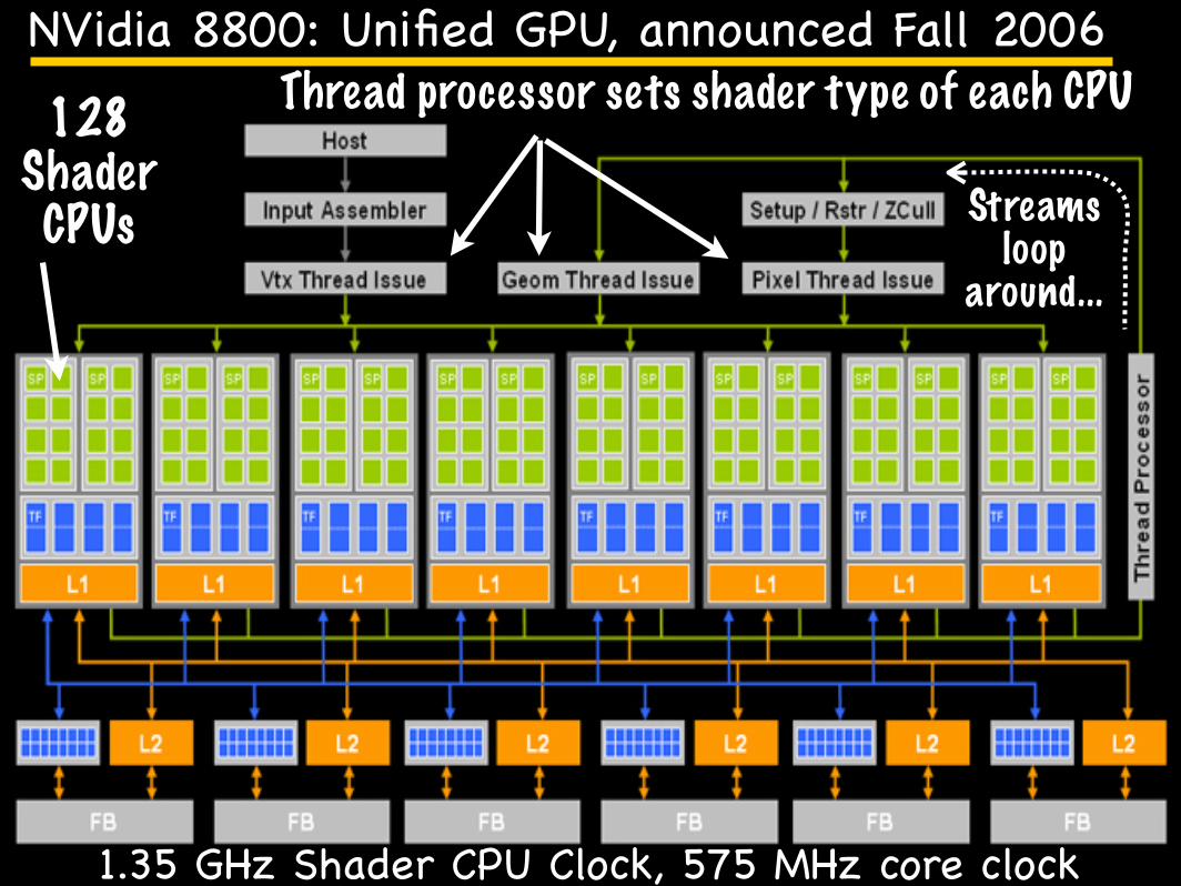
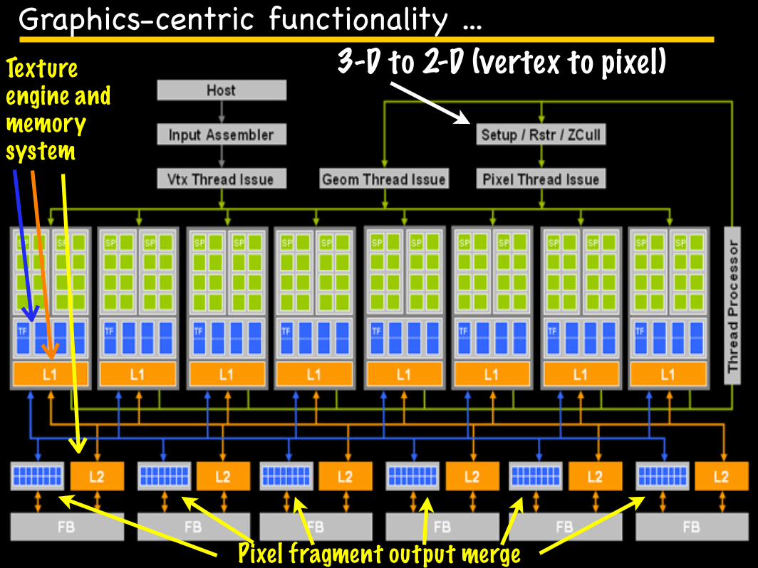
GeForce 8800 Architecture in Detail
Figure 12. GeForce 8800 GTX Block Diagram
TB-02787-001_v1.0 19
NVidia 8800: Unified GPU, announced Fall 2006
128 Shader CPUs Streams
loop around...
Thread processor sets shader type of each CPU
1.35 GHz Shader CPU Clock, 575 MHz core clock
UC Regents Spring 2012 © UCBEECS 150: Graphics Processors
GeForce 8800 Architecture in Detail
Figure 12. GeForce 8800 GTX Block Diagram
TB-02787-001_v1.0 19
Graphics-centric functionality ...3-D to 2-D (vertex to pixel)
Pixel fragment output merge
Texture engine and memory system
UC Regents Spring 2012 © UCBEECS 150: Graphics Processors
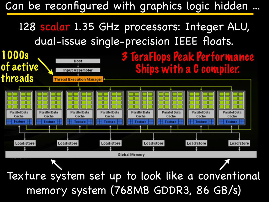
Can be reconfigured with graphics logic hidden ...
128 scalar 1.35 GHz processors: Integer ALU, dual-issue single-precision IEEE floats.
GeForce 8800 Architecture Overview
Figure 9. CUDA Thread Computing Pipeline CUDA enables new applications with a standard platform for extracting valuable
information from vast ;uantities of raw data< and provide the following key benefits
in this area?
! Enables high density computing to be deployed on standard enterprise
workstations and server environments for data intensive applications.
! Divides complex computing tasks into smaller elements that are processed
simultaneously in the GPU to enable real-time decision making.
! Provide a standard platform based on industry-leading NVIDIA hardware and
software for a wide range of high data bandwidth< computationally intensive
applications.
! Combines with multi-core CPU systems to provide a flexible computing
platform.
! Controls complex programs and coordinates inherently parallel computation on
the GPU processed by thousands of computing threads.
CUDAHs high performance< scalable computing architecture solves complex parallel
problems 100x faster than traditional CPU-based architectures?
! Up to of 12L parallel 1.35GHz compute cores in GeQorce LL00 GTX GPUs
harness massive floating point processing power enabling maximum application
performance.
! Thread computing scales across NVIDIAHs complete line of next generation
GPUs - from embedded GPUs to high performance GPUs that support
hundreds of processors.
! NVIDIA SUIV technology allows multiple GPUs to distribute computing to
provide unparalleled compute density.
TB-02787-001_v1.0 13
Texture system set up to look like a conventional memory system (768MB GDDR3, 86 GB/s)
1000s of active threads
3 TeraFlops Peak Performance Ships with a C compiler.
UC Regents Spring 2012 © UCBEECS 150: Graphics Processors
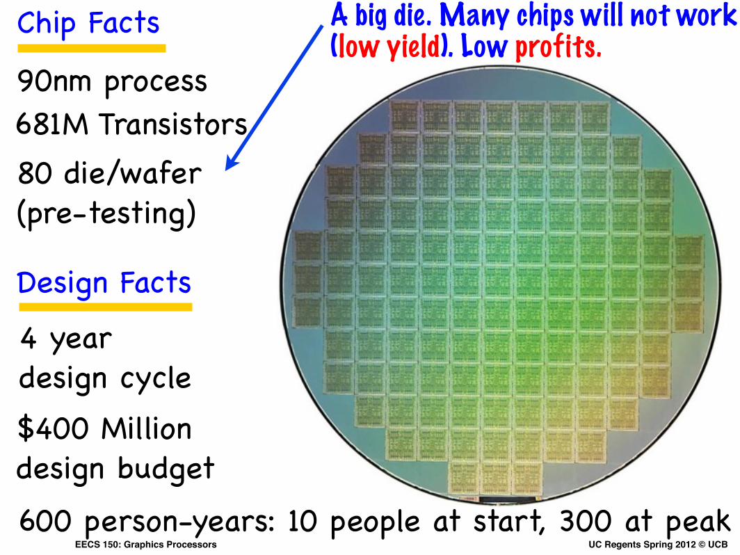
Chip Facts
90nm process681M Transistors80 die/wafer (pre-testing)
A big die. Many chips will not work (low yield). Low profits.
4 year design cycle
Design Facts
$400 Million design budget600 person-years: 10 people at start, 300 at peak
UC Regents Spring 2012 © UCBEECS 150: Graphics Processors
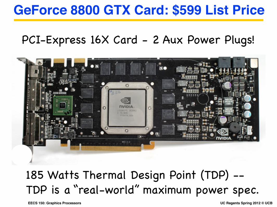
GeForce 8800 GTX Card: $599 List Price
PCI-Express 16X Card - 2 Aux Power Plugs!
185 Watts Thermal Design Point (TDP) -- TDP is a “real-world” maximum power spec.
UC Regents Spring 2012 © UCBEECS 150: Graphics Processors
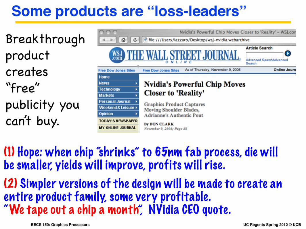
Some products are “loss-leaders”
Breakthrough product creates“free” publicity you can’t buy.
(1) Hope: when chip “shrinks” to 65nm fab process, die will be smaller, yields will improve, profits will rise.(2) Simpler versions of the design will be made to create an entire product family, some very profitable.“We tape out a chip a month”, NVidia CEO quote.

UC Regents Spring 2012 © UCBEECS 150: Graphics Processors
And it happened! 2008 nVidia products
GTX 280
Price similar to 8800, stream CPU count > 2X.
9800 GTX
Specs similar to 8800, card sells for $199.
UC Regents Spring 2012 © UCBEECS 150: Graphics Processors
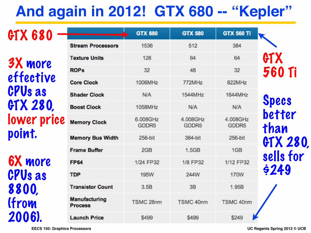
And again in 2012! GTX 680 -- “Kepler”
GTX 560 Ti
Specsbetter than GTX 280, sells for $249
GTX 680
3X more effective CPUs as GTX 280, lower price point.
6X more CPUs as 8800, (from 2006).
UC Regents Spring 2012 © UCBEECS 150: Graphics Processors
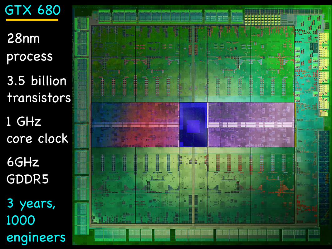
28nm process
3.5 billion transistors
GTX 680
1 GHz core clock
6GHz GDDR5
3 years, 1000 engineers
UC Regents Spring 2012 © UCBEECS 150: Graphics Processors
5
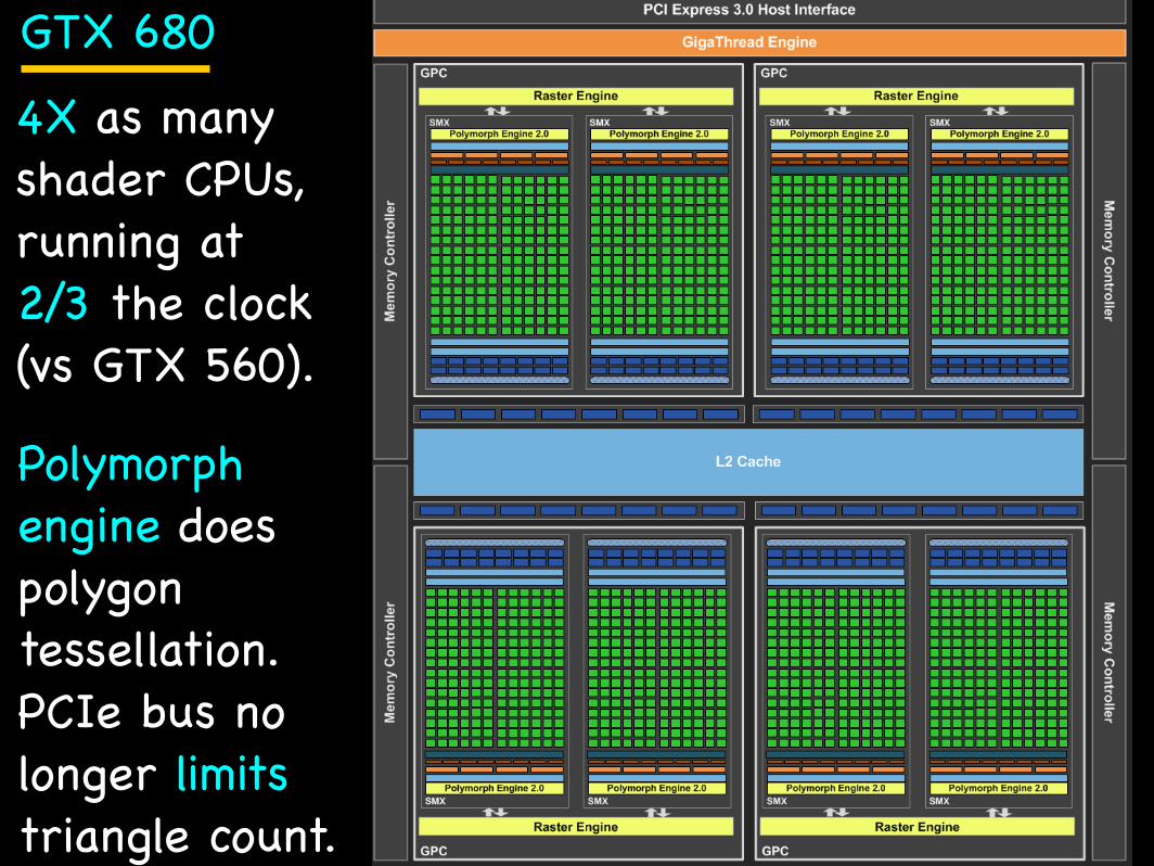
Kepler Architecture In-Depth (GeForce GTX 680) Like Fermi, Kepler GPUs are composed of different configurations of Graphics Processing Clusters (GPCs), Streaming Multiprocessors (SMs), and memory controllers. The GeForce GTX 680 GPU consists of four GPCs, eight next-generation Streaming Multiprocessors (SMX), and four memory controllers.
Figure 1: GeForce GTX 680 Block Diagram
GTX 680
4X as many shader CPUs, running at 2/3 the clock (vs GTX 560).
Polymorph engine does polygon tessellation. PCIe bus nolonger limits triangle count.
UC Regents Spring 2012 © UCBEECS 150: Graphics Processors
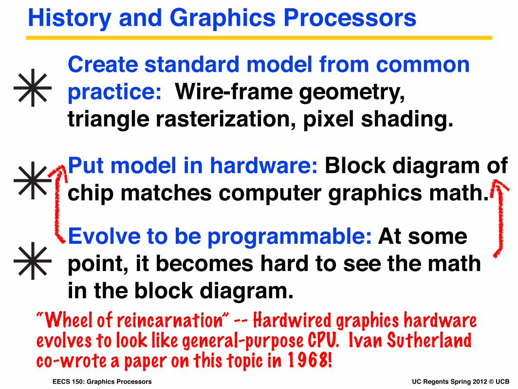
History and Graphics Processors
Create standard model from common practice: Wire-frame geometry, triangle rasterization, pixel shading.
Put model in hardware: Block diagram of chip matches computer graphics math.
Evolve to be programmable: At some point, it becomes hard to see the math in the block diagram.
“Wheel of reincarnation” -- Hardwired graphics hardware evolves to look like general-purpose CPU. Ivan Sutherland co-wrote a paper on this topic in 1968!
UC Regents Spring 2012 © UCBEECS 150: Graphics Processors
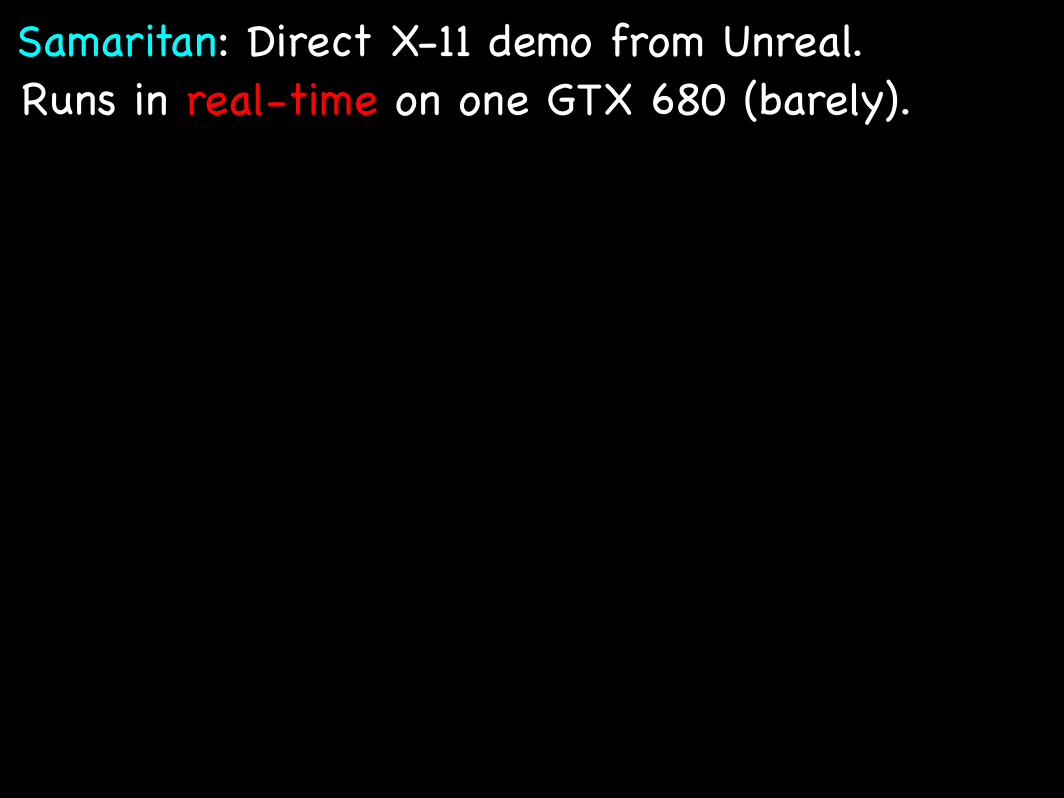
Samaritan: Direct X-11 demo from Unreal.Runs in real-time on one GTX 680 (barely).

UC Regents Spring 2012 © UCBEECS 150: Graphics Processors
UC Regents Spring 2012 © UCBEECS 150: Graphics Processors
GPUs on mobile devices
UC Regents Spring 2012 © UCBEECS 150: Graphics Processors
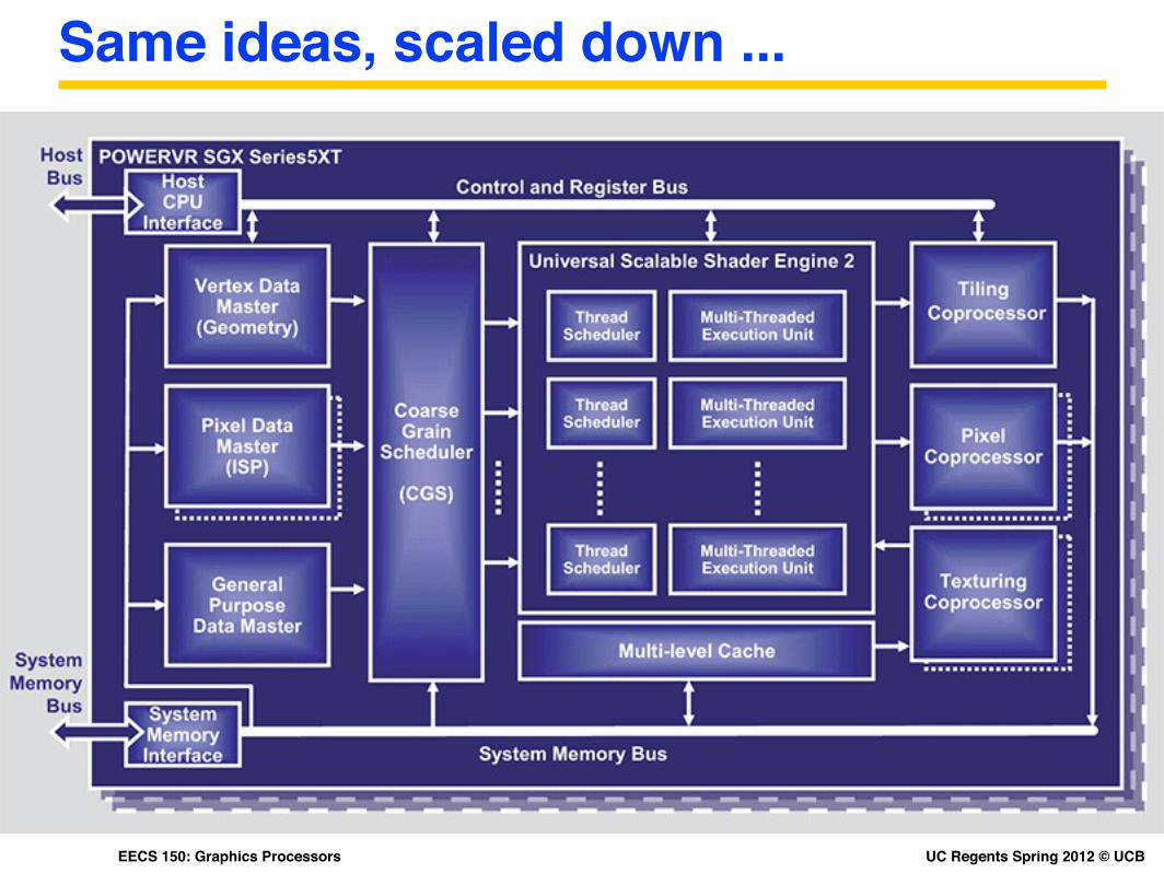
Same ideas, scaled down ...
UC Regents Spring 2012 © UCBCS 150 L24: Power and Energy
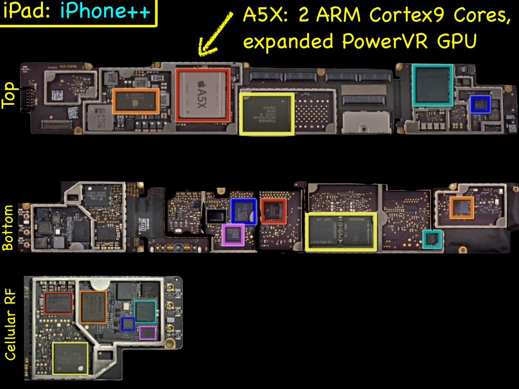
iPad: iPhone++To
pBo
ttom
A5X: 2 ARM Cortex9 Cores, expanded PowerVR GPU
Cellu
lar
RF
UC Regents Spring 2012 © UCBEECS 150: Graphics Processors
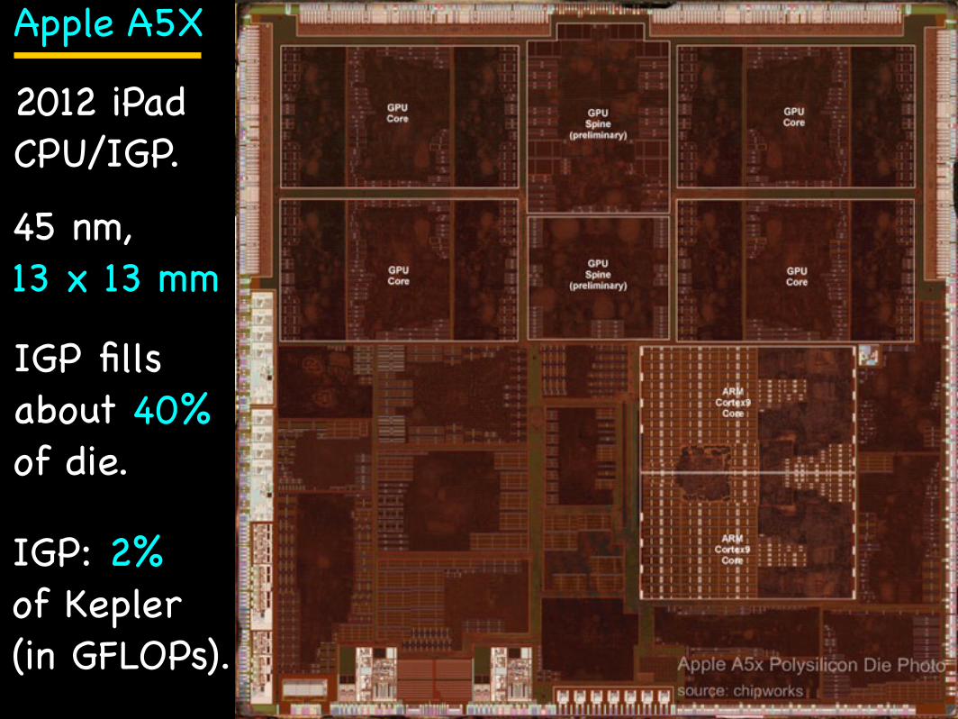
2012 iPad CPU/IGP.
Apple A5X
IGP fills about 40% of die.
45 nm, 13 x 13 mm
IGP: 2% of Kepler (in GFLOPs).

UC Regents Spring 2012 © UCBEECS 150: Graphics Processors
Today: Graphics Processors
Computer Graphics. A brief introduction to “the pipeline”.
Stream Processing. Casting the graphics pipeline into hardware.
Unified Pipelines. GeForce 8800,from Nvidia, introduced in 2006.
Kepler. The latest generation from Nvidia, released last month.