digital output mems accelerometer data sheet adxl362 · digital output mems accelerometer data...
TRANSCRIPT
Micropower, 3-Axis, ±2 g/±4 g/±8 g Digital Output MEMS Accelerometer
Data Sheet ADXL362
Rev. A Document Feedback Information furnished by Analog Devices is believed to be accurate and reliable. However, no responsibility is assumed by Analog Devices for its use, nor for any infringements of patents or other rights of third parties that may result from its use. Specifications subject to change without notice. No license is granted by implication or otherwise under any patent or patent rights of Analog Devices. Trademarks and registered trademarks are the property of their respective owners.
One Technology Way, P.O. Box 9106, Norwood, MA 02062-9106, U.S.A. Tel: 781.329.4700 ©2012 Analog Devices, Inc. All rights reserved. Technical Support www.analog.com
FEATURES Ultralow power
Power can be derived from coin cell battery 1.8 µA @ 100 Hz ODR, 2.0 V supply 3.0 µA @ 400 Hz ODR, 2.0 V supply 270 nA motion activated wake-up mode 10 nA standby current
High resolution: 1 mg/LSB Built-in features for system-level power savings:
Adjustable threshold sleep/wake modes for motion activation
Autonomous interrupt processing, without need for microcontroller intervention, to allow the rest of the system to be turned off completely
Deep embedded FIFO minimizes host processor load Awake state output enables implementation of
standalone, motion activated switch Low noise down to 175 µg/√Hz Wide supply and I/O voltage ranges: 1.6 V to 3.5 V
Operates off 1.8 V to 3.3 V rails Acceleration sample synchronization via external trigger On-chip temperature sensor SPI digital interface Measurement ranges selectable via SPI command Small and thin 3 mm × 3.25 mm × 1.06 mm package
APPLICATIONS Hearing aids Home healthcare devices Motion enabled power save switches Wireless sensors Motion enabled metering devices
GENERAL DESCRIPTION The ADXL362 is an ultralow power, 3-axis MEMS accelerometer that consumes less than 2 µA at a 100 Hz output data rate and 270 nA when in motion triggered wake-up mode. Unlike accelerometers that use power duty cycling to achieve low power consumption, the ADXL362 does not alias input signals by undersampling; it samples the full bandwidth of the sensor at all data rates.
The ADXL362 always provides 12-bit output resolution; 8-bit formatted data is also provided for more efficient single-byte transfers when a lower resolution is sufficient. Measurement ranges of ±2 g, ±4 g, and ±8 g are available, with a resolution of 1 mg/LSB on the ±2 g range. For applications where a noise level lower than the normal 550 µg/√Hz of the ADXL362 is desired, either of two lower noise modes (down to 175 µg/√Hz typical) can be selected at minimal increase in supply current.
In addition to its ultralow power consumption, the ADXL362 has many features to enable true system level power reduction. It includes a deep multimode output FIFO, a built-in micropower temperature sensor, and several activity detection modes including adjustable threshold sleep and wake-up operation that can run as low as 270 nA at a 6 Hz (approximate) measurement rate. A pin output is provided to directly control an external switch when activity is detected, if desired. In addition, the ADXL362 has provisions for external control of sampling time and/or an external clock.
The ADXL362 operates on a wide 1.6 V to 3.5 V supply range, and can interface, if necessary, to a host operating on a separate, lower supply voltage. The ADXL362 is available in a 3 mm × 3.25 mm × 1.06 mm package.
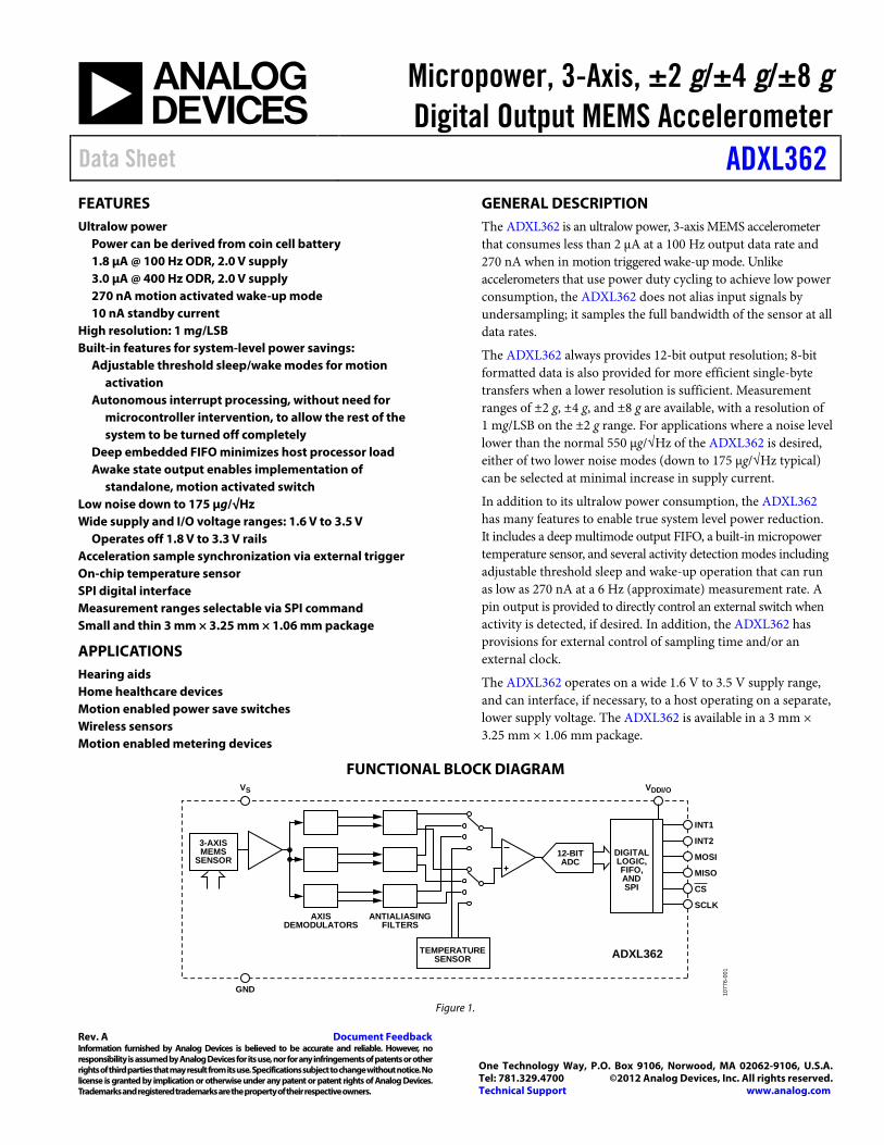
FUNCTIONAL BLOCK DIAGRAM VS VDDI/O
GND
3-AXISMEMS
SENSOR
TEMPERATURESENSOR
AXISDEMODULATORS
ANTIALIASINGFILTERS
ADXL362
12-BITADC
DIGITALLOGIC,FIFO,ANDSPI
INT1
INT2
MOSI
MISO
CS
SCLK
1077
6-00
1
Figure 1.
ADXL362 Data Sheet
Rev. A | Page 2 of 44
TABLE OF CONTENTS Features .............................................................................................. 1 Applications ....................................................................................... 1 General Description ......................................................................... 1 Functional Block Diagram .............................................................. 1 Revision History ............................................................................... 3 Specifications ..................................................................................... 4 Absolute Maximum Ratings ............................................................ 6
Thermal Resistance ...................................................................... 6 Package Information .................................................................... 6 Recommended Soldering Profile ............................................... 6 ESD Caution .................................................................................. 6
Pin Configuration and Function Descriptions ............................. 7 Typical Performance Characteristics ............................................. 8 Theory of Operation ...................................................................... 13
Mechanical Device Operation .................................................. 13 Operating Modes ........................................................................ 13 Selectable Measurement Ranges ............................................... 13 Selectable Output Data Rates .................................................... 13 Power/Noise Tradeoff ................................................................ 14
Power Savings Features .................................................................. 15 Ultralow Power Consumption in All Modes .......................... 15 Motion Detection ....................................................................... 15 FIFO ............................................................................................. 17 Communications ........................................................................ 17
Additional Features ........................................................................ 18 Free Fall Detection ..................................................................... 18 External Clock ............................................................................ 18 Synchronized Data Sampling .................................................... 18 Self Test ........................................................................................ 18 User Register Protection ............................................................ 18 Temperature Sensor ................................................................... 18
Serial Communications ................................................................. 19 SPI Commands ........................................................................... 19 Multibyte Transfers .................................................................... 19 Invalid Addresses and Address Folding .................................. 19 Latency Restrictions ................................................................... 19 Invalid Commands ..................................................................... 19
Register Map .................................................................................... 23 Register Details ............................................................................... 24
Device ID Register ..................................................................... 24 Device ID: 0x1D Register .......................................................... 24 Part ID: 0xF2 Register ................................................................ 24 Silicon Revision ID Register ..................................................... 24 X-Axis Data (8 MSB) Register .................................................. 24 Y-Axis Data (8 MSB) Register .................................................. 24 Z-Axis Data (8 MSB) Register .................................................. 24 Status Register ............................................................................. 25 FIFO Entries Registers ............................................................... 26 X-Axis Data Registers ................................................................ 26 Y-Axis Data Registers ................................................................ 26 Z-Axis Data Registers ................................................................ 26 Temperature Data Registers ...................................................... 26 Soft Reset Register ...................................................................... 26 Activity Threshold Registers ..................................................... 27 Activity Time Register ............................................................... 27 Inactivity Threshold Registers .................................................. 27 Inactivity Time Registers ........................................................... 27 Activity/Inactivity Control Register ........................................ 29 FIFO Control Register ............................................................... 30 FIFO Samples Register .............................................................. 31 INT1/INT2 Function Map Registers ....................................... 31 Filter Control Register ............................................................... 33 Power Control Register ............................................................. 34 Self Test Register ......................................................................... 35
Applications Information .............................................................. 36 Application Examples ................................................................ 36 Power ............................................................................................ 37 FIFO Modes ................................................................................ 38 Interrupts ..................................................................................... 39 Using Synchronized Data Sampling ........................................ 40 Using an External Clock ............................................................ 41 Using Self Test ............................................................................. 41 Operation at Voltages Other Than 2.0 V ................................ 41 Mechanical Considerations for Mounting .............................. 41 Axes of Acceleration Sensitivity ............................................... 42 Layout and Design Recommendations ................................... 42
Outline Dimensions ....................................................................... 43 Ordering Guide .......................................................................... 43
Data Sheet ADXL362
Rev. A | Page 3 of 44
REVISION HISTORY 9/12—Rev. 0 to Rev. A
Moved Revision History Section ..................................................... 3 Changes to Linking Activity and Inactivity Detection Section; Added Figure 31, Figure 32, and Figure 33, Renumbered Sequentially ...................................................................................... 16 Change to Table 13 .......................................................................... 29 Changes to Figure 44 ...................................................................... 36 Moved Power Supply Decoupling Section ................................... 37 Added Power Section, Power Supply Requirements Section, and Figure 47 ........................................................................................... 37 Updated Outline Dimensions ........................................................ 43 Changes to Ordering Guide ........................................................... 43
8/12—Revision 0: Initial Version
ADXL362 Data Sheet
Rev. A | Page 4 of 44
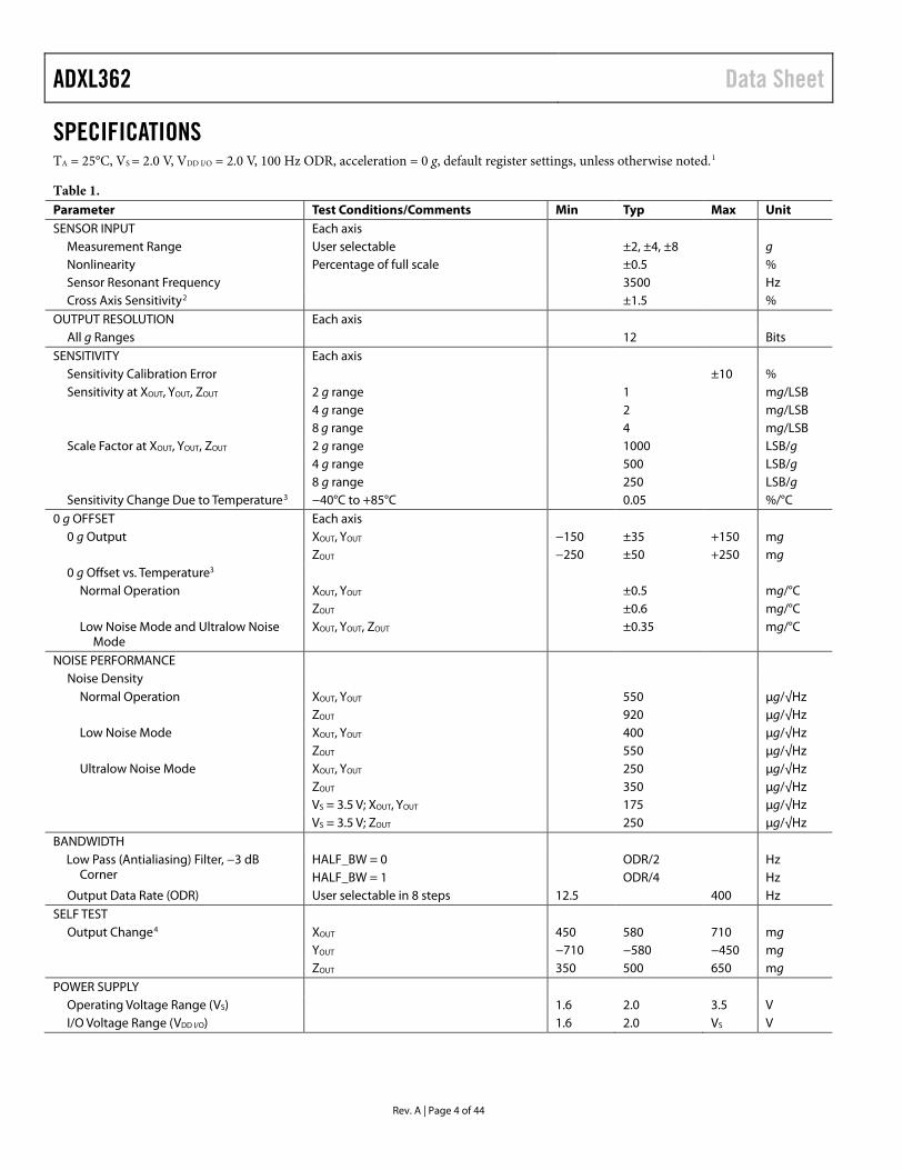
SPECIFICATIONS TA = 25°C, VS = 2.0 V, VDD I/O = 2.0 V, 100 Hz ODR, acceleration = 0 g, default register settings, unless otherwise noted.1
Table 1. Parameter Test Conditions/Comments Min Typ Max Unit SENSOR INPUT Each axis
Measurement Range User selectable ±2, ±4, ±8 g Nonlinearity Percentage of full scale ±0.5 % Sensor Resonant Frequency 3500 Hz Cross Axis Sensitivity2 ±1.5 %
OUTPUT RESOLUTION Each axis All g Ranges 12 Bits
SENSITIVITY Each axis Sensitivity Calibration Error ±10 % Sensitivity at XOUT, YOUT, ZOUT 2 g range 1 mg/LSB 4 g range 2 mg/LSB 8 g range 4 mg/LSB Scale Factor at XOUT, YOUT, ZOUT 2 g range 1000 LSB/g 4 g range 500 LSB/g 8 g range 250 LSB/g Sensitivity Change Due to Temperature3 −40°C to +85°C 0.05 %/°C
0 g OFFSET Each axis 0 g Output XOUT, YOUT −150 ±35 +150 mg ZOUT −250 ±50 +250 mg 0 g Offset vs. Temperature3
Normal Operation XOUT, YOUT ±0.5 mg/°C ZOUT ±0.6 mg/°C
Low Noise Mode and Ultralow Noise Mode
XOUT, YOUT, ZOUT ±0.35 mg/°C
NOISE PERFORMANCE Noise Density
Normal Operation XOUT, YOUT 550 µg/√Hz ZOUT 920 µg/√Hz
Low Noise Mode XOUT, YOUT 400 µg/√Hz ZOUT 550 µg/√Hz
Ultralow Noise Mode XOUT, YOUT 250 µg/√Hz ZOUT 350 µg/√Hz
VS = 3.5 V; XOUT, YOUT 175 µg/√Hz VS = 3.5 V; ZOUT 250 µg/√Hz
BANDWIDTH Low Pass (Antialiasing) Filter, −3 dB
Corner HALF_BW = 0 ODR/2 Hz HALF_BW = 1 ODR/4 Hz
Output Data Rate (ODR) User selectable in 8 steps 12.5 400 Hz SELF TEST
Output Change4 XOUT 450 580 710 mg YOUT −710 −580 −450 mg ZOUT 350 500 650 mg
POWER SUPPLY Operating Voltage Range (VS) 1.6 2.0 3.5 V I/O Voltage Range (VDD I/O) 1.6 2.0 VS V
Data Sheet ADXL362
Rev. A | Page 5 of 44
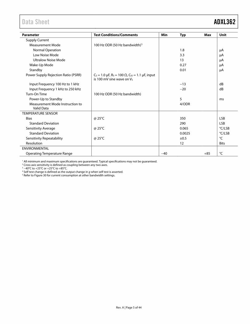
Parameter Test Conditions/Comments Min Typ Max Unit Supply Current
Measurement Mode 100 Hz ODR (50 Hz bandwidth)5 Normal Operation 1.8 µA Low Noise Mode 3.3 µA Ultralow Noise Mode 13 µA
Wake-Up Mode 0.27 µA Standby 0.01 µA
Power Supply Rejection Ratio (PSRR) CS = 1.0 µF, RS = 100 Ω, CIO = 1.1 µF, input is 100 mV sine wave on VS
Input Frequency 100 Hz to 1 kHz −13 dB Input Frequency 1 kHz to 250 kHz −20 dB
Turn-On Time 100 Hz ODR (50 Hz bandwidth) Power-Up to Standby 5 ms Measurement Mode Instruction to
Valid Data 4/ODR
TEMPERATURE SENSOR Bias @ 25°C 350 LSB
Standard Deviation 290 LSB Sensitivity Average @ 25°C 0.065 °C/LSB
Standard Deviation 0.0025 °C/LSB Sensitivity Repeatability @ 25°C ±0.5 °C Resolution 12 Bits
ENVIRONMENTAL Operating Temperature Range −40 +85 °C
1 All minimum and maximum specifications are guaranteed. Typical specifications may not be guaranteed. 2 Cross axis sensitivity is defined as coupling between any two axes. 3 −40°C to +25°C or +25°C to +85°C. 4 Self test change is defined as the output change in g when self test is asserted. 5 Refer to Figure 30 for current consumption at other bandwidth settings.
ADXL362 Data Sheet
Rev. A | Page 6 of 44
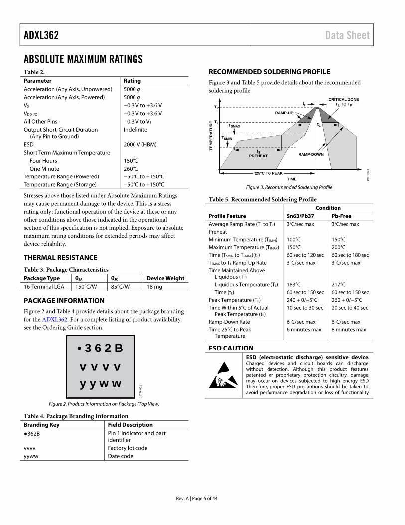
ABSOLUTE MAXIMUM RATINGS Table 2. Parameter Rating Acceleration (Any Axis, Unpowered) 5000 g Acceleration (Any Axis, Powered) 5000 g VS −0.3 V to +3.6 V VDD I/O −0.3 V to +3.6 V All Other Pins −0.3 V to VS Output Short-Circuit Duration
(Any Pin to Ground) Indefinite
ESD 2000 V (HBM) Short Term Maximum Temperature
Four Hours 150°C One Minute 260°C
Temperature Range (Powered) −50°C to +150°C Temperature Range (Storage) −50°C to +150°C
Stresses above those listed under Absolute Maximum Ratings may cause permanent damage to the device. This is a stress rating only; functional operation of the device at these or any other conditions above those indicated in the operational section of this specification is not implied. Exposure to absolute maximum rating conditions for extended periods may affect device reliability.
THERMAL RESISTANCE
Table 3. Package Characteristics Package Type θJA θJC Device Weight 16-Terminal LGA 150°C/W 85°C/W 18 mg
PACKAGE INFORMATION Figure 2 and Table 4 provide details about the package branding for the ADXL362. For a complete listing of product availability, see the Ordering Guide section.
• 3 6 2 Bv v v vy y w w
1077
6-00
2
Figure 2. Product Information on Package (Top View)
Table 4. Package Branding Information Branding Key Field Description
362B Pin 1 indicator and part identifier
vvvv Factory lot code yyww Date code
RECOMMENDED SOLDERING PROFILE Figure 3 and Table 5 provide details about the recommended soldering profile.
tP
tL
t25°C TO PEAK
tSPREHEAT
CRITICAL ZONETL TO TP
TEM
PER
ATU
RE
TIME
RAMP-DOWN
RAMP-UP
TSMIN
TSMAX
TP
TL
1077
6-00
3
Figure 3. Recommended Soldering Profile
Table 5. Recommended Soldering Profile
Profile Feature
Condition
Sn63/Pb37 Pb-Free Average Ramp Rate (TL to TP) 3°C/sec max 3°C/sec max Preheat Minimum Temperature (TSMIN) 100°C 150°C Maximum Temperature (TSMAX) 150°C 200°C Time (TSMIN to TSMAX)(tS) 60 sec to 120 sec 60 sec to 180 sec TSMAX to TL Ramp-Up Rate 3°C/sec max 3°C/sec max Time Maintained Above
Liquidous (TL)
Liquidous Temperature (TL) 183°C 217°C Time (tL) 60 sec to 150 sec 60 sec to 150 sec
Peak Temperature (TP) 240 + 0/−5°C 260 + 0/−5°C Time Within 5°C of Actual
Peak Temperature (tP) 10 sec to 30 sec 20 sec to 40 sec
Ramp-Down Rate 6°C/sec max 6°C/sec max Time 25°C to Peak
Temperature 6 minutes max 8 minutes max
ESD CAUTION
Data Sheet ADXL362
Rev. A | Page 7 of 44
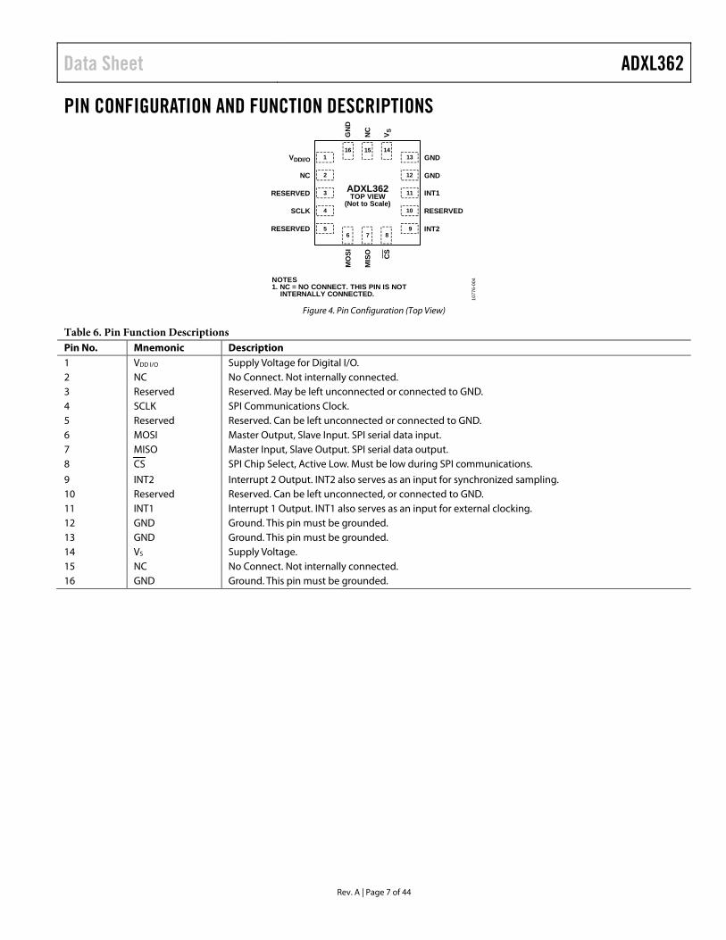
PIN CONFIGURATION AND FUNCTION DESCRIPTIONS
NC
GN
D
V S
MIS
O
MO
SI CS
NOTES1. NC = NO CONNECT. THIS PIN IS NOT INTERNALLY CONNECTED.
NC
VDDI/O
RESERVED
SCLK
RESERVED
GND
GND
INT1
RESERVED
INT2
ADXL362TOP VIEW
(Not to Scale)
1
2
3
4
5
13
12
11
10
96 7 8
16 15 14
1077
6-00
4
Figure 4. Pin Configuration (Top View)
Table 6. Pin Function Descriptions Pin No. Mnemonic Description 1 VDD I/O Supply Voltage for Digital I/O. 2 NC No Connect. Not internally connected. 3 Reserved Reserved. May be left unconnected or connected to GND. 4 SCLK SPI Communications Clock. 5 Reserved Reserved. Can be left unconnected or connected to GND. 6 MOSI Master Output, Slave Input. SPI serial data input. 7 MISO Master Input, Slave Output. SPI serial data output. 8 CS SPI Chip Select, Active Low. Must be low during SPI communications.
9 INT2 Interrupt 2 Output. INT2 also serves as an input for synchronized sampling. 10 Reserved Reserved. Can be left unconnected, or connected to GND. 11 INT1 Interrupt 1 Output. INT1 also serves as an input for external clocking. 12 GND Ground. This pin must be grounded. 13 GND Ground. This pin must be grounded. 14 VS Supply Voltage. 15 NC No Connect. Not internally connected. 16 GND Ground. This pin must be grounded.
ADXL362 Data Sheet
Rev. A | Page 8 of 44
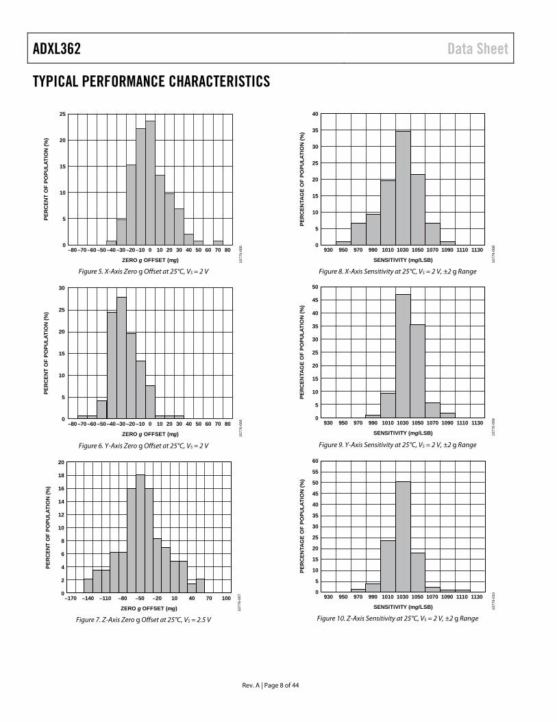
TYPICAL PERFORMANCE CHARACTERISTICS
25
20
15
10
5
0
PER
CEN
T O
F PO
PULA
TIO
N (%
)
–80–70–60–50–40–30–20–10 0 10 20 30 40 50 60 70 80
ZERO g OFFSET (mg) 1077
6-00
5
Figure 5. X-Axis Zero g Offset at 25°C, VS = 2 V
PER
CEN
T O
F PO
PULA
TIO
N (%
)
–80–70–60–50–40–30–20–10 0 10 20 30 40 50 60 70 80
ZERO g OFFSET (mg)
0
5
10
15
20
25
30
1077
6-00
6
Figure 6. Y-Axis Zero g Offset at 25°C, VS = 2 V
ZERO g OFFSET (mg)
0
2
4
6
8
10
12
14
16
18
20
–170 –140 –110 –80 –50 –20 10 40 70 100
PER
CEN
T O
F PO
PULA
TIO
N (%
)
1077
6-00
7
Figure 7. Z-Axis Zero g Offset at 25°C, VS = 2.5 V
40
35
30
25
20
15
10
5
0
PER
CEN
TAG
E O
F PO
PULA
TIO
N (%
)
SENSITIVITY (mg/LSB)
930 950 970 990 1010 1030 1050 1070 1090 1110 1130
1077
6-00
8
Figure 8. X-Axis Sensitivity at 25°C, VS = 2 V, ±2 g Range
50
45
40
35
30
25
20
15
10
5
0
PER
CEN
TAG
E O
F PO
PULA
TIO
N (%
)
SENSITIVITY (mg/LSB)
930 950 970 990 1010 1030 1050 1070 1090 1110 1130
1077
6-00
9
Figure 9. Y-Axis Sensitivity at 25°C, VS = 2 V, ±2 g Range
60
45
50
55
40
35
30
25
20
15
10
5
0
PER
CEN
TAG
E O
F PO
PULA
TIO
N (%
)
SENSITIVITY (mg/LSB)
930 950 970 990 1010 1030 1050 1070 1090 1110 1130
1077
6-01
0
Figure 10. Z-Axis Sensitivity at 25°C, VS = 2 V, ±2 g Range
Data Sheet ADXL362
Rev. A | Page 9 of 44
0
5
10
15
20
25
–1.0 –0.8 –0.6 –0.4 –0.2 0 0.2 0.4 0.6 0.8 1.0
PER
CEN
T O
F PO
PULA
TIO
N (%
)
ZERO g OFFSET TEMPERATURE COEFFICIENT (mg/°C) 1077
6-01
1
Figure 11. X-Axis Zero g Offset Temperature Coefficient, VS = 2.5 V
–1.0 –0.8 –0.6 –0.4 –0.2 0 0.2 0.4 0.6 0.8 1.00
5
10
15
20
25
30
35
PER
CEN
T O
F PO
PULA
TIO
N (%
)
ZERO g OFFSET TEMPERATURE COEFFICIENT (mg/°C) 1077
6-01
2
Figure 12. Y-Axis Zero g Offset Temperature Coefficient, VS = 2.5 V
0
5
10
15
20
25
–0.5 –0.3 –0.1 0.1 0.3 0.5 0.7 0.9 1.1 1.3 1.5 1.7 1.9
PER
CEN
T O
F PO
PULA
TIO
N (%
)
ZERO g OFFSET TEMPERATURE COEFFICIENT (mg/°C) 1077
6-01
3
Figure 13. Z-Axis Zero g Offset Temperature Coefficient, VS = 2.5 V
–60
–50
–40
–30
–20
–10
0
10
20
30
40
50
–60 –40 –20 0 20 40 60 80 100
OU
TPU
T(m
g)
TEMPERATURE (°C) 1077
6-01
4
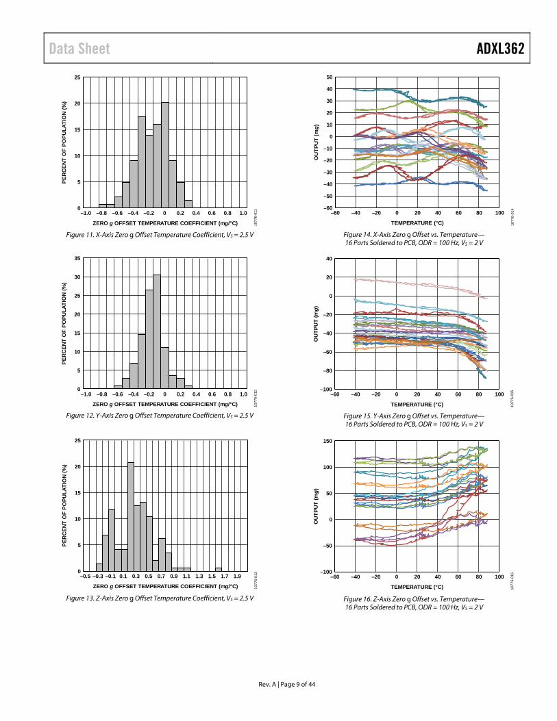
Figure 14. X-Axis Zero g Offset vs. Temperature— 16 Parts Soldered to PCB, ODR = 100 Hz, VS = 2 V
–100
–80
–60
–40
–20
0
20
40
–60 –40 –20 0 20 40 60 80 100
OU
TPU
T (m
g)
TEMPERATURE (°C) 1077
6-01
5
Figure 15. Y-Axis Zero g Offset vs. Temperature— 16 Parts Soldered to PCB, ODR = 100 Hz, VS = 2 V
–100
–50
0
50
100
150
–60 –40 –20 0 20 40 60 80 100
OU
TPU
T (m
g)
TEMPERATURE (°C) 1077
6-01
6
Figure 16. Z-Axis Zero g Offset vs. Temperature— 16 Parts Soldered to PCB, ODR = 100 Hz, VS = 2 V
ADXL362 Data Sheet
Rev. A | Page 10 of 44
–10
–8
–6
–4
–2
0
2
4
6
8
10
–60 –40 –20 0 20 40 60 80 100
SEN
SITI
VITY
DEV
IATI
ON
FR
OM
25°
C (%
)
TEMPERATURE (°C) 1077
6-01
7
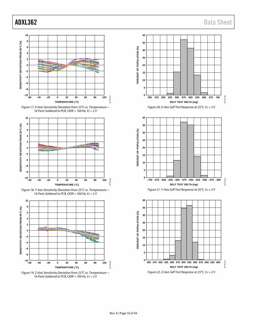
Figure 17. X-Axis Sensitivity Deviation from 25°C vs. Temperature—
16 Parts Soldered to PCB, ODR = 100 Hz, VS = 2 V
TEMPERATURE (°C)
–10
–8
–6
–4
–2
0
2
4
6
8
10
–60 –40 –20 0 20 40 60 80 100
SEN
SITI
VITY
DEV
IATI
ON
FR
OM
25°
C (%
)
1077
6-01
8
Figure 18. Y-Axis Sensitivity Deviation from 25°C vs. Temperature—
16 Parts Soldered to PCB, ODR = 100 Hz, VS = 2 V
–10
–8
–6
–4
–2
0
2
4
6
8
10
–60 –40 –20 0 20 40 60 80 100
SEN
SITI
VITY
DEV
IATI
ON
FR
OM
25°C
(%)
TEMPERATURE (°C) 1077
6-01
9
Figure 19. Z-Axis Sensitivity Deviation from 25°C vs. Temperature—
16 Parts Soldered to PCB, ODR = 100 Hz, VS = 2 V
0
5
10
15
20
25
30
35
40
450 475 500 525 550 575 600 625 650 675 700
PER
CEN
T O
F PO
PULA
TIO
N (%
)
SELF TEST DELTA (mg) 1077
6-02
0
Figure 20. X-Axis Self Test Response at 25°C, VS = 2 V
0
5
10
15
20
25
30
35
40
–700 –675 –650 –625 –600 –575 –550 –525 –500 –475 –450
PER
CEN
T O
F PO
PULA
TIO
N (%
)
SELF TEST DELTA (mg) 1077
6-02
1
Figure 21. Y-Axis Self Test Response at 25°C, VS = 2 V
0
5
10
15
20
25
30
35
40
350 375 400 425 450 475 500 525 550 575 600 625 650
PER
CEN
T O
F PO
PULA
TIO
N (%
)
SELF TEST DELTA (mg) 1077
6-02
2
Figure 22. Z-Axis Self Test Response at 25°C, VS = 2 V
Data Sheet ADXL362
Rev. A | Page 11 of 44
0
5
10
15
20
25
30
35
1.50 1.55 1.60 1.65 1.70 1.75 1.80 1.85 1.90 1.95 2.00 2.05
CURRENT CONSUMPTION (µA)
PER
CEN
T O
F PO
PULA
TIO
N (%
)
1077
6-02
3
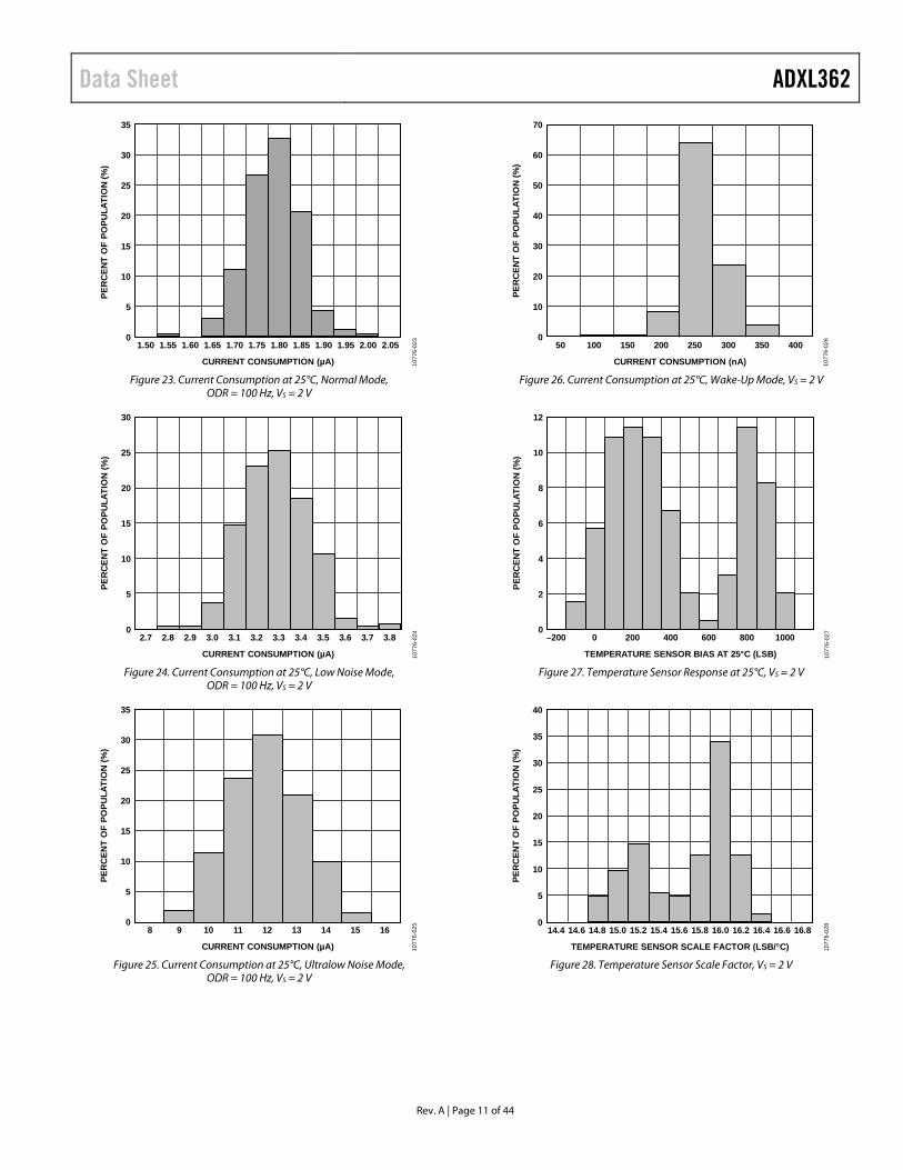
Figure 23. Current Consumption at 25°C, Normal Mode,
ODR = 100 Hz, VS = 2 V
PER
CEN
T O
F PO
PULA
TIO
N (%
)
0
5
10
15
20
25
30
2.7 2.8 2.9 3.0 3.1 3.2 3.3 3.4 3.5 3.6 3.7 3.8
CURRENT CONSUMPTION (µA) 1077
6-02
4
Figure 24. Current Consumption at 25°C, Low Noise Mode,
ODR = 100 Hz, VS = 2 V
PER
CEN
T O
F PO
PULA
TIO
N (%
)
0
5
10
15
20
25
30
35
8 9 10 11 12 13 14 15 16
CURRENT CONSUMPTION (µA) 1077
6-02
5
Figure 25. Current Consumption at 25°C, Ultralow Noise Mode,
ODR = 100 Hz, VS = 2 V
PER
CEN
T O
F PO
PUL A
TIO
N (%
)
0
10
20
30
40
50
60
70
50 100 150 200 250 300 350 400
CURRENT CONSUMPTION (nA) 1077
6-02
6
Figure 26. Current Consumption at 25°C, Wake-Up Mode, VS = 2 V
0
2
4
6
8
10
12
–200 0 200 400 600 800 1000
PER
CEN
T O
F PO
PULA
TIO
N (%
)
TEMPERATURE SENSOR BIAS AT 25°C (LSB) 1077
6-02
7
Figure 27. Temperature Sensor Response at 25°C, VS = 2 V
0
5
10
15
20
25
30
35
40
14.4 14.6 14.8 15.0 15.2 15.4 15.6 15.8 16.0 16.2 16.4 16.6 16.8
PER
CEN
T O
F PO
PULA
TIO
N (%
)
TEMPERATURE SENSOR SCALE FACTOR (LSB/°C) 1077
6-02
8
Figure 28. Temperature Sensor Scale Factor, VS = 2 V
ADXL362 Data Sheet
Rev. A | Page 12 of 44
0
5
10
15
20
25
30
–20 –16 –12 –8 –4 0 4 8 12 16 20
PER
CEN
T O
F PO
PULA
TIO
N (%
)
CLOCK FREQUENCY DEVIATION FROM IDEAL (%) 1077
6-02
9
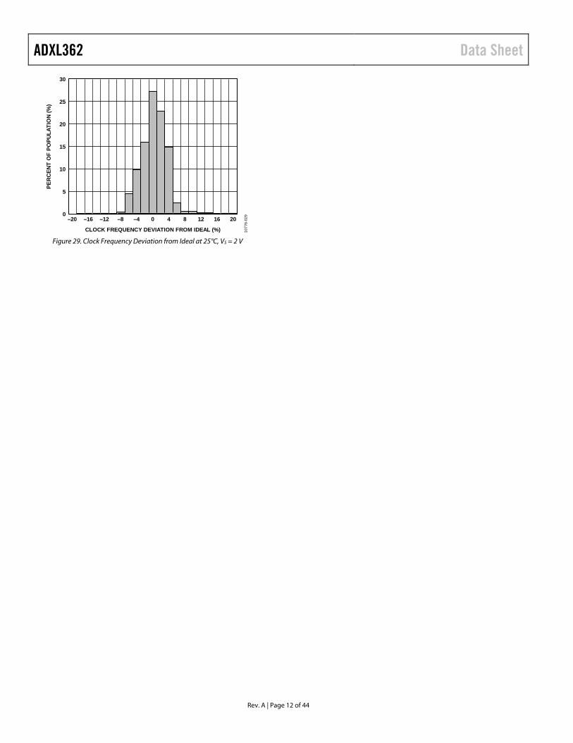
Figure 29. Clock Frequency Deviation from Ideal at 25°C, VS = 2 V
Data Sheet ADXL362
Rev. A | Page 13 of 44
THEORY OF OPERATION The ADXL362 is a complete 3-axis acceleration measurement system that operates at extremely low power consumption levels. It measures both dynamic acceleration, resulting from motion or shock, and static acceleration, such as tilt. Acceleration is reported digitally and the device communicates via the SPI protocol. Built-in digital logic enables autonomous operation and implements functionality that enhances system level power savings.
MECHANICAL DEVICE OPERATION The moving component of the sensor is a polysilicon surface-micromachined structure that is built on top of a silicon wafer. Polysilicon springs suspend the structure over the surface of the wafer and provide a resistance against acceleration forces.
Deflection of the structure is measured using differential capacitors that consist of independent fixed plates and plates attached to the moving mass. Acceleration deflects the structure and unbalances the differential capacitor, resulting in a sensor output whose amplitude is proportional to acceleration. Phase sensitive demodulation determines the magnitude and polarity of the acceleration.
OPERATING MODES The ADXL362 has two operating modes: measurement mode for continuous, wide bandwidth sensing; and wake-up mode for limited bandwidth activity detection. In addition, measurement can be suspended altogether by placing the device in standby.
Measurement Mode
Measurement mode is the normal operating mode of the ADXL362. In this mode, acceleration data is read continuously and the accelerometer consumes less than 3 µA (typical) across its entire range of output data rates of up to 400 Hz using a 2.0 V supply. All features described in this datasheet are available when operating the ADXL362 in this mode.
The ability to continuously output data from the minimum 12.5 Hz to the maximum 400 Hz data rate while still delivering less than 3 µA (typical) of current consumption is what defines the ADXL362 as an ultralow power accelerometer. Other accel-erometers derive low current by using a specific low power mode that power cycles acceleration sensing. The result is a small effective bandwidth in the low power modes and undersampling of input data; therefore, unwanted aliasing can occur. Under-sampling and aliasing do not occur with the ADXL362 because it continuously samples the full bandwidth of its sensor at all data rates.
Wake-Up Mode
Wake-up mode is ideal for simple detection of the presence or absence of motion at extremely low power consumption (270 nA at a 2.0 V supply voltage). Wake-up mode is useful particularly for implementation of a motion activated on/off switch, allowing the rest of the system to be powered down until activity is detected.
Wake-up mode reduces current consumption to a very low level by measuring acceleration only about six times per second to determine whether motion is present. If motion is detected, the accelerometer can respond autonomously in the following ways:
• Switch into full bandwidth measurement mode • Signal an interrupt to a microcontroller • Wake up downstream circuitry, depending on the
configuration In wake-up mode, all accelerometer features are available with the exception of the activity timer. All registers can be accessed, and real-time data can be read and/or stored in the FIFO.
Standby
Placing the ADXL362 in standby suspends measurement and reduces current consumption to 10 nA (typical). Pending interrupts and data are preserved and no new interrupts are generated.
The ADXL362 powers up in standby with all sensor functions turned off.
SELECTABLE MEASUREMENT RANGES The ADXL362 has selectable measurement ranges of ±2 g, ±4 g, and ±8 g. Acceleration samples are always converted by a 12-bit ADC; therefore, sensitivity scales with g range. Ranges and corresponding sensitivity values are listed in Table 1.
When acceleration exceeds the measurement extremes, data is clipped at the full-scale value (0x0FFF), and no damage is caused to the accelerometer. Table 2 lists the absolute maximum ratings for acceleration, indicating the acceleration level that can cause permanent damage to the device.
SELECTABLE OUTPUT DATA RATES The ADXL362 can report acceleration data at various data rates ranging from 12.5 Hz to 400 Hz. The internal low-pass filter pole is automatically set to ¼ or ½ the selected ODR (based on the HALF_BW setting) to ensure the Nyquist sampling criterion is met and no aliasing occurs.
ADXL362 Data Sheet
Rev. A | Page 14 of 44
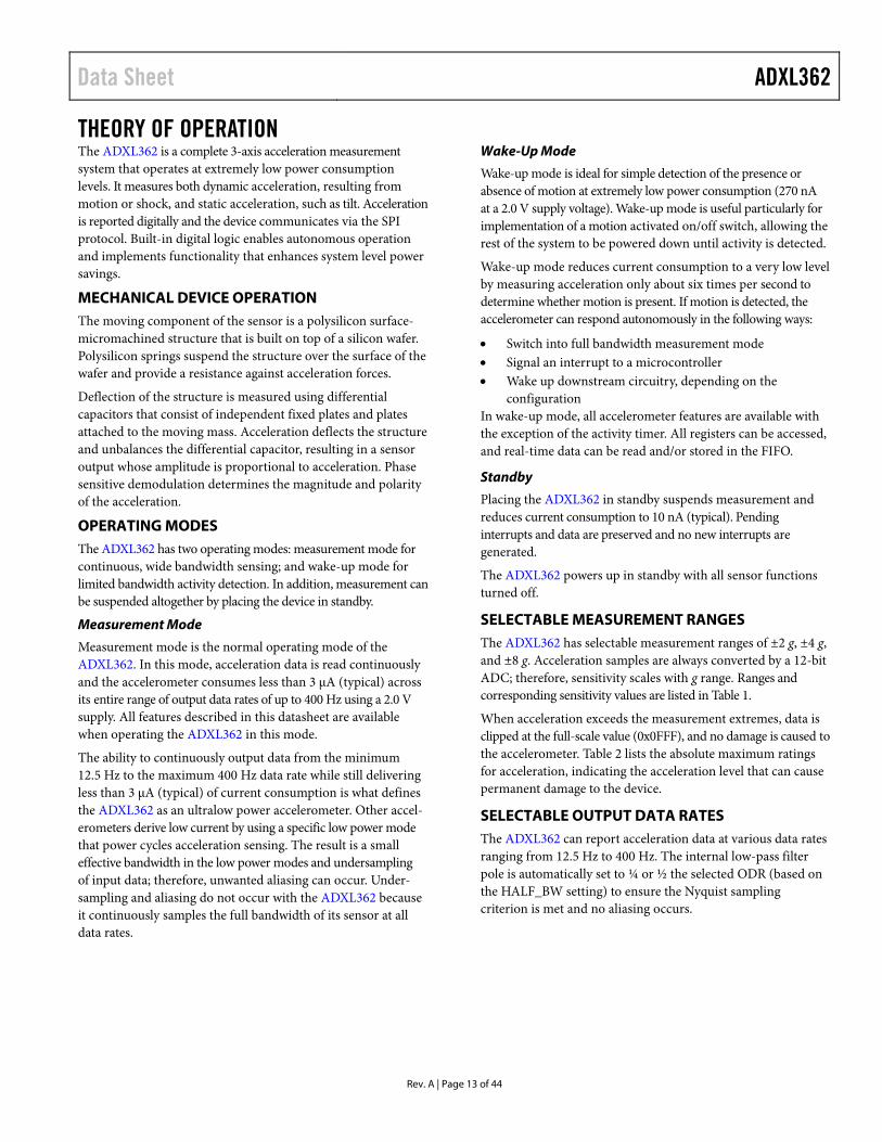
Current consumption varies somewhat with output data rate as shown in Figure 30, remaining below 5.0 µA over the entire range of data rates and operating voltages.
6
5
4
3
2
1
0
CU
RR
ENT
CO
NSU
MPT
ION
(µA
)
OUTPUT DATA RATE (Hz)
0 100 200 300 400
VS = 1.6VVS = 2.0VVS = 2.5VVS = 3.0VVS = 3.5V
1077
6-03
0
Figure 30. Current Consumption vs. Output Data Rate at Several
Supply Voltages
Antialiasing
The analog-to-digital converter (ADC) of the ADXL362 samples at the (user selected) output data rate. In the absence of anti-aliasing filtering, it aliases any input signals whose frequency is more than half the data rate. To mitigate this, a two-pole low-pass filter is provided at the input of the ADC.
The user can set this antialiasing filter to a bandwidth that is at ½ the data rate or ¼ the data rate. Setting the antialiasing filter pole to ½ of the output data rate provides less aggressive antialiasing filtering, but maximizes bandwidth and is adequate for most applications. Setting the pole to ¼ of the data rate reduces bandwidth for a given data rate, but provides more aggressive antialiasing.
The antialiasing filter of the ADXL362 defaults to the more conservative setting, where bandwidth is set to one-fourth the output data rate.
POWER/NOISE TRADEOFF The ADXL362 offers a few options for decreasing noise at the expense of only a small increase in current consumption.
The noise performance of the ADXL362 in normal operation, typically 7 LSB rms at 100 Hz bandwidth, is adequate for most applications, depending upon bandwidth and the desired reso-lution. For cases where lower noise is needed, the ADXL362 provides two lower noise operating modes that trade reduced noise for a somewhat higher current consumption.
Table 7 lists the current consumption and noise densities obtained for normal operation and the two lower noise modes at a typical 2.0 V supply.
Table 7. Noise and Current Consumption: Normal Operation, Low Noise Mode, and Ultralow Noise Mode @ VS = 2.0 V
Mode
Noise (µg/√Hz) Typical
Current Consumption (µA) Typical
Normal Operation 550 1.8 Low Noise 400 3.0 Ultralow Noise 250 10
Operating the ADXL362 at a higher supply voltage also decreases noise. Table 8 lists the current consumption and noise densities obtained for normal operation and the two lower noise modes at the highest recommended supply, 3.3 V.
Table 8. Noise and Current Consumption: Normal Operation, Low Noise Mode, and Ultralow Noise Mode @ VS = 3.3 V
Mode
Noise (µg/√Hz) Typical
Current Consumption (µA) Typical
Normal Operation 380 2.7 Low Noise 280 4.5 Ultralow Noise 175 15

Data Sheet ADXL362
Rev. A | Page 15 of 44
POWER SAVINGS FEATURES Designed for the most power conscious applications, the ADXL362 includes several features (as described in this section) for enabling power savings at the system level, as well as at the device level.
ULTRALOW POWER CONSUMPTION IN ALL MODES At the device level, the most obvious power saving feature of the ADXL362 is its ultralow current consumption in all configurations. The ADXL362 consumes between 1.1 µA (typical) and 5 µA (typical) across all data rates up to 400 Hz and all supply voltages up to 3.5 V (see Figure 30). An even lower power, 270 nA (typical) motion triggered wake-up mode is provided for simple motion detection applications that require a power consumption lower than 1 µA.
At these current levels, the accelerometer consumes less power in full operation than the standby currents of many other system components, and is, therefore, optimal for applications that require continuous acceleration monitoring and very long battery life. Because the accelerometer is always on, it can act as a motion activation switch. The accelerometer signals to the rest of the system when to turn on, thereby managing power at the system level.
As important as its low operating current, the 10 nA (typical) standby current of the ADXL362 contributes to a much longer battery life in applications that spend most of their time in a sleep state and wake up via an external trigger.
MOTION DETECTION The ADXL362 features built-in logic that detects activity (presence of acceleration above a threshold) and inactivity (lack of acceleration above a threshold). Activity and inactivity events can be used as triggers to manage the accelerometer mode of operation, trigger an interrupt to a host processor, and/or autonomously drive a motion switch.
Detection of an activity or inactivity event is indicated in the status register and can be configured to generate an interrupt. In addition, the activity status of the device, that is, whether it is moving or stationary, is indicated by the AWAKE bit, described in the Using the AWAKE Bit section.
Activity and inactivity detection can be used when the accel-erometer is in either measurement mode or wake-up mode.
Activity Detection
An activity event is detected when acceleration remains above a specified threshold for a specified time period.
Referenced and Absolute Configurations
Activity detection can be configured as referenced or absolute.
When using absolute activity detection, acceleration samples are compared to a user set threshold to determine whether motion is present. For example, if a threshold of 0.5 g is set and the acceleration on the z-axis is 1 g for longer than the user defined activity time, the activity status asserts.
In many applications, it is advantageous for activity detection to be based not on an absolute threshold, but on a deviation from a reference point or orientation. This is particularly useful because it removes the effect on activity detection of the static 1 g imposed by gravity. When an accelerometer is stationary, its output can reach 1 g, even when it is not moving. In absolute activity, when the threshold is set to less than 1 g, activity is immediately detected in this case.
In the referenced configuration, activity is detected when acceleration samples are at least a user set amount above an internally defined reference for the user defined amount of time, as described in Equation 1.
ABS(Acceleration − Reference) > Threshold (1)
Consequently, activity is detected only when the acceleration has deviated sufficiently from the initial orientation. The reference for activity detection is calculated when activity detection is engaged in the following scenarios: • When the activity function is turned on and measurement
mode is engaged; • If link mode is enabled: when inactivity is detected and
activity detection begins; or • If link mode is not enabled: when activity is detected and
activity detection repeats.
The referenced configuration results in a very sensitive activity detection that detects even the most subtle motion events.
Fewer False Positives
Ideally, the intent of activity detection is to wake up a system only when motion is intentional, ignoring noise or small, unintentional movements. In addition to being sensitive to subtle motion events, the ADXL362 activity detection algorithm is designed to be robust in filtering out undesired triggers.
The ADXL362 activity detection functionality includes a timer to filter out unwanted motion and ensure that only sustained motion is recognized as activity. The duration of this timer, as well as the acceleration threshold, are user adjustable from one sample (that is, no timer) to up to 20 seconds of motion.
Note that the activity timer is operational in measurement mode only. In wake-up mode, one-sample activity detection is used.
Inactivity Detection
An inactivity event is detected when acceleration remains below a specified threshold for a specified time. Inactivity detection is also configurable as referenced or absolute.
When using absolute inactivity detection, acceleration samples are compared to a user set threshold for the user set time to determine the absence of motion. Inactivity is detected when enough consecutive samples are all below the threshold. The absolute configuration of inactivity should be used for implementing free fall detection.
ADXL362 Data Sheet
Rev. A | Page 16 of 44
When using referenced inactivity detection, inactivity is detected when acceleration samples are within a user specified amount of an internally defined reference (as described by Equation 2) for a user defined amount of time.
ABS(Acceleration − Reference) < Threshold (2)
Referenced inactivity, like referenced activity, is particularly useful for eliminating the effects of the static acceleration due to gravity. With absolute inactivity, if the inactivity threshold is set lower than 1 g, a device resting motionless may never detect inactivity. With referenced inactivity, the same device under the same configuration detects inactivity.
The inactivity timer can be set to anywhere from 2.5 ms (a single sample at 400 Hz ODR) to almost 90 minutes (65,535 samples at 12.5 Hz ODR) of inactivity. A requirement for inactivity detec-tion is that for whatever period of time the inactivity timer has been configured, the accelerometer detects inactivity only when it has been stationary for that amount of time.
For example, if the accelerometer has been configured for 90 minutes, the accelerometer detects inactivity when it has been stationary for 90 minutes. The wide range of timer settings means that in applications where power conservation is critical, the system can be put to sleep after very short periods of inactivity. In applications where continuous operation is critical, the system stays on for as long as any motion is present.
Linking Activity and Inactivity Detection
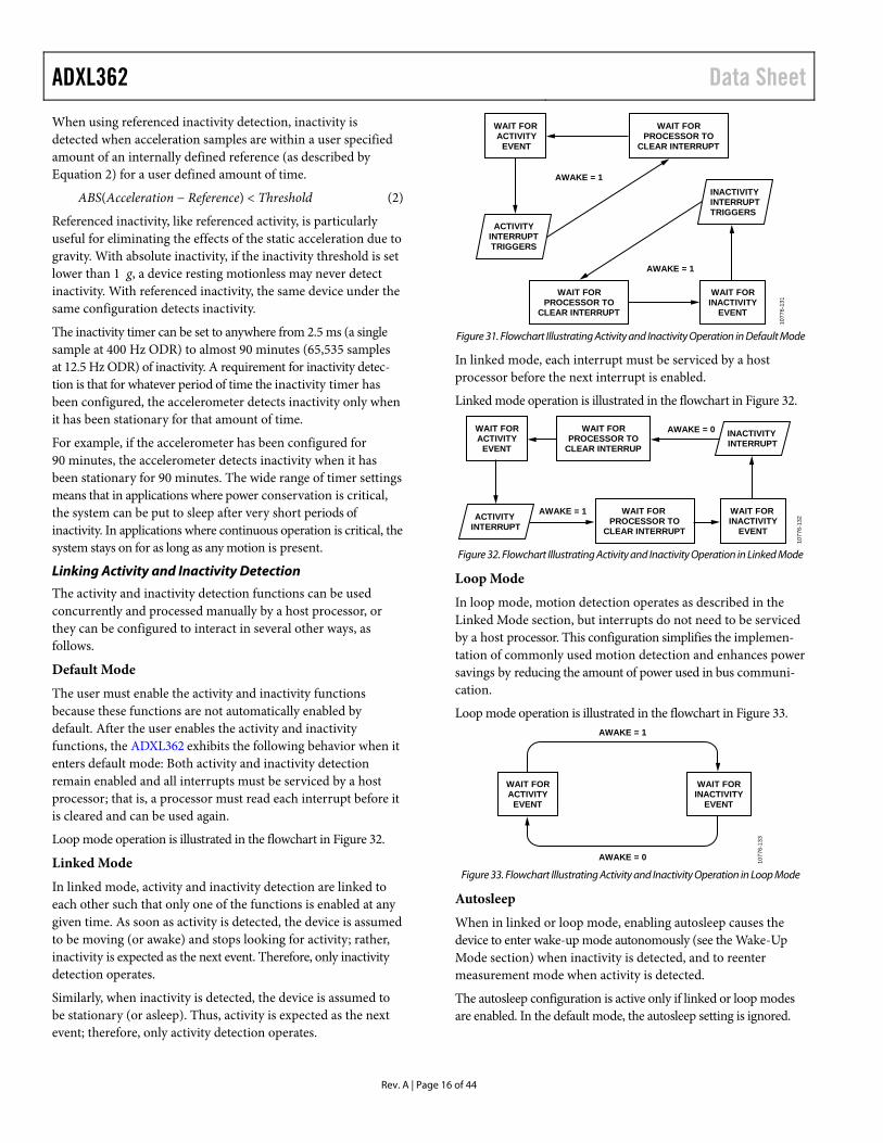
The activity and inactivity detection functions can be used concurrently and processed manually by a host processor, or they can be configured to interact in several other ways, as follows.
Default Mode
The user must enable the activity and inactivity functions because these functions are not automatically enabled by default. After the user enables the activity and inactivity functions, the ADXL362 exhibits the following behavior when it enters default mode: Both activity and inactivity detection remain enabled and all interrupts must be serviced by a host processor; that is, a processor must read each interrupt before it is cleared and can be used again.
Loop mode operation is illustrated in the flowchart in Figure 32.
Linked Mode
In linked mode, activity and inactivity detection are linked to each other such that only one of the functions is enabled at any given time. As soon as activity is detected, the device is assumed to be moving (or awake) and stops looking for activity; rather, inactivity is expected as the next event. Therefore, only inactivity detection operates.
Similarly, when inactivity is detected, the device is assumed to be stationary (or asleep). Thus, activity is expected as the next event; therefore, only activity detection operates.
WAIT FORACTIVITY
EVENT
ACTIVITYINTERRUPTTRIGGERS
WAIT FORINACTIVITY
EVENT
INACTIVITYINTERRUPTTRIGGERS
WAIT FORPROCESSOR TO
CLEAR INTERRUPT
WAIT FORPROCESSOR TO
CLEAR INTERRUPT
AWAKE = 1
AWAKE = 1
1077
6-13
1
Figure 31. Flowchart Illustrating Activity and Inactivity Operation in Default Mode
In linked mode, each interrupt must be serviced by a host processor before the next interrupt is enabled.
Linked mode operation is illustrated in the flowchart in Figure 32.
WAIT FORACTIVITY
EVENT
ACTIVITYINTERRUPT
WAIT FORINACTIVITY
EVENT
INACTIVITYINTERRUPT
AWAKE = 0
AWAKE = 1
WAIT FORPROCESSOR TO
CLEAR INTERRUP
WAIT FORPROCESSOR TO
CLEAR INTERRUPT
1077
6-13
2
Figure 32. Flowchart Illustrating Activity and Inactivity Operation in Linked Mode
Loop Mode
In loop mode, motion detection operates as described in the Linked Mode section, but interrupts do not need to be serviced by a host processor. This configuration simplifies the implemen-tation of commonly used motion detection and enhances power savings by reducing the amount of power used in bus communi-cation.
Loop mode operation is illustrated in the flowchart in Figure 33.
WAIT FORACTIVITY
EVENT
WAIT FORINACTIVITY
EVENT
AWAKE = 0
AWAKE = 1
1077
6-13
3
Figure 33. Flowchart Illustrating Activity and Inactivity Operation in Loop Mode
Autosleep
When in linked or loop mode, enabling autosleep causes the device to enter wake-up mode autonomously (see the Wake-Up Mode section) when inactivity is detected, and to reenter measurement mode when activity is detected.
The autosleep configuration is active only if linked or loop modes are enabled. In the default mode, the autosleep setting is ignored.
Data Sheet ADXL362
Rev. A | Page 17 of 44
Using the AWAKE Bit
The AWAKE bit is a status bit that indicates whether the ADXL362 is awake or asleep. The device is awake when it has experienced an activity condition, and it is asleep when it has experienced an inactivity condition.
The awake signal can be mapped to the INT1 or INT2 pin, allowing the pin to serve as a status output to connect or dis-connect power to downstream circuitry based on the awake status of the accelerometer. Used in conjunction with loop mode, this configuration implements a trivial, autonomous motion activated switch, as shown in Figure 43.
If the turn-on time of downstream circuitry can be tolerated, this motion switch configuration can save significant system level power by eliminating the standby current consumption of the remainder of the application. This standby current can often exceed the full operating current of the ADXL362.
FIFO The ADXL362 includes a deep 512-sample first in, first out (FIFO) buffer. The FIFO provides benefits primarily in two ways, as follows.
System Level Power Savings
Appropriate use of the FIFO enables system level power savings by enabling the host processor to sleep for extended periods of time while the accelerometer autonomously collects data. Alter-natively, using the FIFO to collect data can unburden the host while it tends to other tasks.
Data Recording/Event Context
The FIFO can be used in a triggered mode to record all data leading up to an activity detection event, thereby providing con-text for the event. In the case of a system that identifies impact events, for example, the accelerometer can keep the entire system off while it stores acceleration data in its FIFO and looks for an activity event. When the impact event occurs, data that was collected prior to the event is frozen in the FIFO. The accel-erometer can then wake the rest of the system and transfer this data to the host processor, thereby providing context for the impact event.
Generally, the more context available, the more intelligent decisions a system can achieve, making a deep FIFO especially useful. The ADXL362 FIFO can store up to more than 13 seconds of data, providing a clear picture of events prior to an activity trigger.
All FIFO modes of operation, as well as the structure of the FIFO and instructions for retrieving data from it, are described in further detail in the FIFO Modes section of this data sheet.
COMMUNICATIONS SPI Instructions
The digital interface of the ADXL362 is implemented with system level power savings in mind. The following features enhance power savings:
• Burst reads and writes reduce the number of SPI communication cycles required to configure the part and retrieve data.
• Concurrent operation of activity and inactivity detection enables “set it and forget it” operation. Linked and loop modes further reduce communications power by enabling the clearing of interrupts without processor intervention.
• The FIFO is implemented such that consecutive samples can be read continuously via a multibyte read of unlimited length; thus, one read FIFO instruction can clear the entire contents of the FIFO. In many other accelerometers, each read instruction retrieves a single sample only. In addition, the ADXL362 FIFO construction allows the use of direct memory access (DMA) to read the FIFO contents.
Bus Keepers
The ADXL362 includes bus keepers on all digital interface pins: MISO, MOSI, SCLK, CS, INT1, and INT2. Bus keepers are used to prevent tristate bus lines from floating when nothing is driving them, thus preventing through current in any gate inputs that are on the bus.
MSB Registers
Acceleration and temperature measurements are converted to 12-bit values and transmitted via SPI using two registers per measurement. To read a full sample set of 3-axis acceleration data, six registers must be read.
Many applications do not require the accuracy that 12-bit data provides and prefer, instead, to save system level power. The MSB registers XDATA, YDATA, and ZDATA enable this tradeoff. These registers contain the eight MSBs of the x-, y-, and z-axis acceleration data; reading them effectively provides 8-bit accel-eration values. Importantly, only three (consecutive) registers must be read to retrieve a full data set, significantly reducing the time during which the SPI bus is active and drawing current.
12-bit and 8-bit data are available simultaneously so that both data formats can be used in a single application, depending on the needs of the application at a given time. For example, the pro-cessor can read 12-bit data when higher resolution is required, and switch to 8-bit data (simply by reading a different set of registers) when application requirements change.
ADXL362 Data Sheet
Rev. PrA Page 4 of 8
ADDITIONAL FEATURES FREE FALL DETECTION Many digital output accelerometers include a built-in free fall detection feature. In the ADXL362, this function can be imple-mented using the inactivity interrupt. Refer to the Applications Information section for more details, including suggested threshold and timing values.
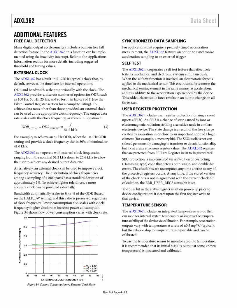
EXTERNAL CLOCK The ADXL362 has a built-in 51.2 kHz (typical) clock that, by default, serves as the time base for internal operations.
ODR and bandwidth scale proportionally with the clock. The ADXL362 provides a discrete number of options for ODR, such as 100 Hz, 50 Hz, 25 Hz, and so forth, in factors of 2, (see the Filter Control Register section for a complete listing). To achieve data rates other than those provided, an external clock can be used at the appropriate clock frequency. The output data rate scales with the clock frequency, as shown in Equation 3.
kHz2.51f
ODRODR SELECTEDACTUAL ×= (3)
For example, to achieve an 80 Hz ODR, select the 100 Hz ODR setting and provide a clock frequency that is 80% of nominal, or 41.0 kHz.
The ADXL362 can operate with external clock frequencies ranging from the nominal 51.2 kHz down to 25.6 kHz to allow the user to achieve any desired output data rate.
Alternatively, an external clock can be used to improve clock frequency accuracy. The distribution of clock frequencies among a sampling of >1000 parts has a standard deviation of approximately 3%. To achieve tighter tolerances, a more accurate clock can be provided externally.
Bandwidth automatically scales to ½ or ¼ of the ODR (based on the HALF_BW setting), and this ratio is preserved, regardless of clock frequency. Power consumption also scales with clock frequency: higher clock rates increase power consumption. Figure 34 shows how power consumption varies with clock rate.
3.0
2.5
2.0
1.5
1.0
0.5
0
CU
RR
ENT
CO
NSU
MPT
ION
(µA
)
EXTERNAL CLOCK FREQUENCY (kHz)
43 44 45 46 47 48 49 50 51 52
VS = 1.6VVS = 2.0VVS = 3.5V
1077
6-03
1
Figure 34. Current Consumption vs. External Clock Rate
SYNCHRONIZED DATA SAMPLING For applications that require a precisely timed acceleration measurement, the ADXL362 features an option to synchronize acceleration sampling to an external trigger.
SELF TEST The ADXL362 incorporates a self test feature that effectively tests its mechanical and electronic systems simultaneously. When the self test function is invoked, an electrostatic force is applied to the mechanical sensor. This electrostatic force moves the mechanical sensing element in the same manner as acceleration, and it is additive to the acceleration experienced by the device. This added electrostatic force results in an output change on all three axes.
USER REGISTER PROTECTION The ADXL362 includes user register protection for single event upsets (SEUs). An SEU is a change of state caused by ions or electromagnetic radiation striking a sensitive node in a micro-electronic device. The state change is a result of the free charge created by ionization in or close to an important node of a logic element (for example, a memory bit). The SEU, itself, is not con-sidered permanently damaging to transistor or circuit functionality, but it can create erroneous register values. The ADXL362 registers that are protected from SEU are Register 0x20 to Register 0x2E.
SEU protection is implemented via a 99-bit error correcting (Hamming-type) code that detects both single- and double-bit errors. The check bits are recomputed any time a write to any of the protected registers occurs. At any time, if the stored version of the check bits is not in agreement with the current check bit calculation, the ERR_USER_REGS status bit is set.
The SEU bit in the status register is set on power-up prior to device configuration; it clears upon the first register write to that device.
TEMPERATURE SENSOR The ADXL362 includes an integrated temperature sensor that can monitor internal system temperature or improve the tempera-ture stability of the device via calibration. For example, acceleration outputs vary with temperature at a rate of ±0.5 mg/°C (typical), but the relationship to temperature is repeatable and can be calibrated.
To use the temperature sensor to monitor absolute temperature, it is recommended that its initial bias (its output at some known temperature) is measured and calibrated.
Data Sheet ADXL362
Rev. A | Page 19 of 44
SERIAL COMMUNICATIONS The ADXL362 communicates via a 4-wire SPI and operates as a slave. Ignore data that is transmitted from the ADXL362 to the master device during writes to the ADXL362.
As shown in Figure 36 to Figure 40, the MISO pin is in a high impedance state, held by a bus keeper, except when the ADXL362 is sending read data (to conserve bus power).
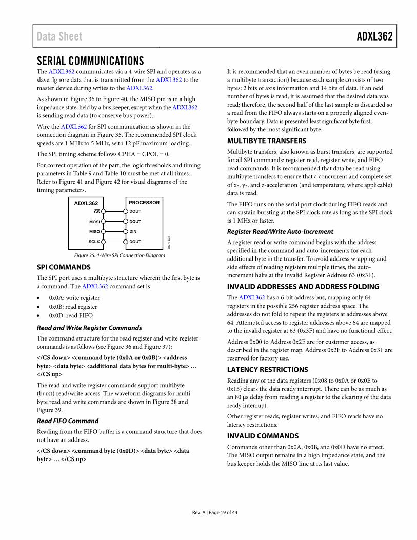
Wire the ADXL362 for SPI communication as shown in the connection diagram in Figure 35. The recommended SPI clock speeds are 1 MHz to 5 MHz, with 12 pF maximum loading.
The SPI timing scheme follows CPHA = CPOL = 0.
For correct operation of the part, the logic thresholds and timing parameters in Table 9 and Table 10 must be met at all times. Refer to Figure 41 and Figure 42 for visual diagrams of the timing parameters.
ADXL362 PROCESSOR
CS
MOSI
MISO
SCLK
DOUT
DOUT
DIN
DOUT
1077
6-03
2
Figure 35. 4-Wire SPI Connection Diagram
SPI COMMANDS The SPI port uses a multibyte structure wherein the first byte is a command. The ADXL362 command set is
• 0x0A: write register • 0x0B: read register • 0x0D: read FIFO
Read and Write Register Commands
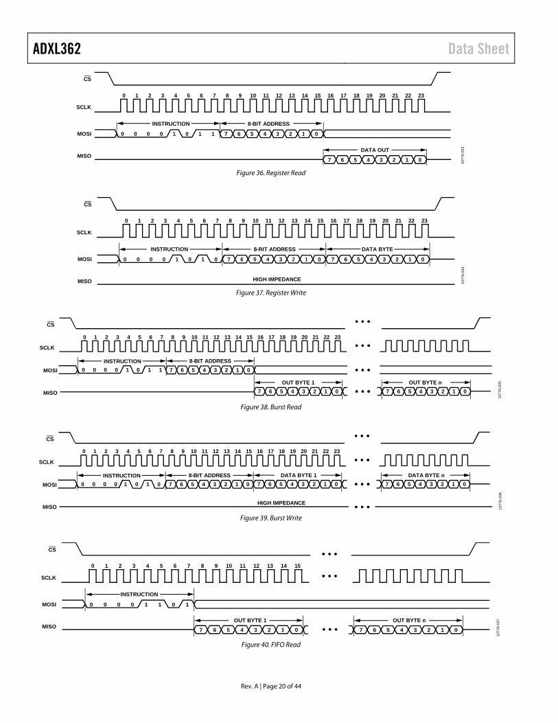
The command structure for the read register and write register commands is as follows (see Figure 36 and Figure 37):
</CS down> <command byte (0x0A or 0x0B)> <address byte> <data byte> <additional data bytes for multi-byte> … </CS up>
The read and write register commands support multibyte (burst) read/write access. The waveform diagrams for multi-byte read and write commands are shown in Figure 38 and Figure 39.
Read FIFO Command
Reading from the FIFO buffer is a command structure that does not have an address.
</CS down> <command byte (0x0D)> <data byte> <data byte> … </CS up>
It is recommended that an even number of bytes be read (using a multibyte transaction) because each sample consists of two bytes: 2 bits of axis information and 14 bits of data. If an odd number of bytes is read, it is assumed that the desired data was read; therefore, the second half of the last sample is discarded so a read from the FIFO always starts on a properly aligned even-byte boundary. Data is presented least significant byte first, followed by the most significant byte.
MULTIBYTE TRANSFERS Multibyte transfers, also known as burst transfers, are supported for all SPI commands: register read, register write, and FIFO read commands. It is recommended that data be read using multibyte transfers to ensure that a concurrent and complete set of x-, y-, and z-acceleration (and temperature, where applicable) data is read.
The FIFO runs on the serial port clock during FIFO reads and can sustain bursting at the SPI clock rate as long as the SPI clock is 1 MHz or faster.
Register Read/Write Auto-Increment
A register read or write command begins with the address specified in the command and auto-increments for each additional byte in the transfer. To avoid address wrapping and side effects of reading registers multiple times, the auto-increment halts at the invalid Register Address 63 (0x3F).
INVALID ADDRESSES AND ADDRESS FOLDING The ADXL362 has a 6-bit address bus, mapping only 64 registers in the possible 256 register address space. The addresses do not fold to repeat the registers at addresses above 64. Attempted access to register addresses above 64 are mapped to the invalid register at 63 (0x3F) and have no functional effect.
Address 0x00 to Address 0x2E are for customer access, as described in the register map. Address 0x2F to Address 0x3F are reserved for factory use.
LATENCY RESTRICTIONS Reading any of the data registers (0x08 to 0x0A or 0x0E to 0x15) clears the data ready interrupt. There can be as much as an 80 µs delay from reading a register to the clearing of the data ready interrupt.
Other register reads, register writes, and FIFO reads have no latency restrictions.
INVALID COMMANDS Commands other than 0x0A, 0x0B, and 0x0D have no effect. The MISO output remains in a high impedance state, and the bus keeper holds the MISO line at its last value.
ADXL362 Data Sheet
Rev. A | Page 20 of 44
0 1 5432 6 7 8 9 10 11 12 13 14 15 16 17 18 19 20 21 22 23
711010000 6 5 4 3 2 1 0
INSTRUCTION 8-BIT ADDRESS
DATA OUT
7 6 5 4 3 2 1 0
CS
SCLK
MOSI
MISO
777 66666667770000 00 10 1 000 7 555
8 B
5
8
5
I BI
5
BI T
5 444
T AD
4
T
4
D D
4
D D
4 333
DRES
3
D
3
S S
3
ES S
3 222
S
2
S
222 11111 0000000111
1077
6-03
3
Figure 36. Register Read
0 1 5432 6 7 8 9 10 11 12 13 14 15 16 17 18 19 20 21 22 23
701010000 6 5 4 3 2 1 0
INSTRUCTION 8-BIT ADDRESS
7 6 5 4 3 2 1 0
DATA BYTE
CS
SCLK
MOSI
MISO
7777 66666 5
8 B B
5
B BI
5555 4
IT A ABI A
4
A
3
D
444 3
DDR D E RE
23
RE ES
333 2
SS S
2222 111 0
HIGH IMPEDANCE
1077
6-03
4
Figure 37. Register Write
0 1 5432 6 7 8 9 10 11 12 13 14 15 16 17 18 19 20 21 22 23
71010000 6 5 4 3 2 1 0INSTRUCTION 8-BIT ADDRESS
CS
SCLK
1
OUT BYTE 1 OUT BYTE n
MOSI
MISO 7 6 5 4 3 2 1 0 7 6 5 4 3 2 1 0
1077
6-03
5
Figure 38. Burst Read
HIGH IMPEDANCE
0 1 5432 6 7 8 9 10 11 12 13 14 15 16 17 18 19 20 21 22 23
71010000 6 5 4 3 2 1 0INSTRUCTION 8-BIT ADDRESS
CS
SCLK
0MOSI
MISO
DATA BYTE 1 DATA BYTE n7 6 5 4 3 2 1 0 7 6 5 4 3 2 1 0
1077
6-03
6
Figure 39. Burst Write
0 1 5432 6 7 8 9 10 11 12 13 14 15
10110000
INSTRUCTION
CS
SCLK
MOSI
MISO 7 6 5 4 3 2 1 0 7 6 5 4 3 2 1 0777 666 555 444 333 222 11 0
OUT BYTE 1 OUT BYTE n
1077
6-03
7
Figure 40. FIFO Read
Data Sheet ADXL362
Rev. A | Page 21 of 44
MISO
SCLK
MOSI MSB IN LSB IN
HIGH IMPEDANCE
tCSD
tCSH tCLDtCLE
tSU tHD
tFtRCSS
1077
6-03
8
CS
Figure 41. Timing Diagram for SPI Write Instructions
MISO
SCLK
MOSI MSB OUT
DON’T CARE
LSB OUT
tHIGH tLOW tCSH
tDIStHOtV
1077
6-03
9
CS
Figure 42. Timing Diagram for SPI Read Instructions
Table 9. SPI Digital Input/Output Limit1 Parameter Test Conditions/Comments Min Max Unit Digital Input
Low Level Input Voltage (VIL) 0.3 × VDD I/O V High Level Input Voltage (VIH) 0.7 × VDD I/O V Low Level Input Current (IIL) VIN = VDD I/O 0.1 µA High Level Input Current (IIH) VIN = 0 V −0.1 µA
Digital Output Low Level Output Voltage (VOL) IOL = 10 mA 0.2 × VDD I/O V High Level Output Voltage (VOH) IOH = −4 mA 0.8 × VDD I/O V Low Level Output Current (IOL) VOL = VOL, max 10 mA High Level Output Current (IOH) VOH = VOH, min −4 mA
1 Limits based on characterization results, not production tested.
ADXL362 Data Sheet
Rev. A | Page 22 of 44
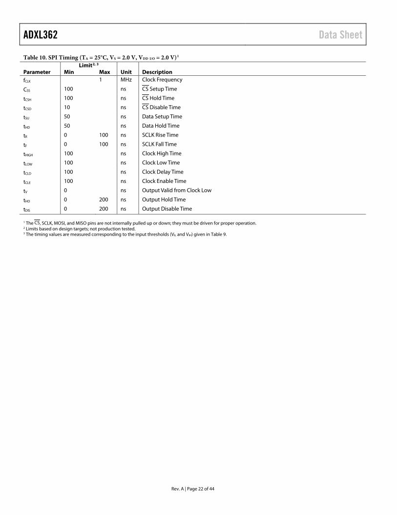
Table 10. SPI Timing (TA = 25°C, VS = 2.0 V, VDD I/O = 2.0 V)1 Limit2, 3 Parameter Min Max Unit Description fCLK 1 MHz Clock Frequency
CSS 100 ns CS Setup Time
tCSH 100 ns CS Hold Time
tCSD 10 ns CS Disable Time
tSU 50 ns Data Setup Time
tHD 50 ns Data Hold Time
tR 0 100 ns SCLK Rise Time
tF 0 100 ns SCLK Fall Time
tHIGH 100 ns Clock High Time
tLOW 100 ns Clock Low Time
tCLD 100 ns Clock Delay Time
tCLE 100 ns Clock Enable Time
tV 0 ns Output Valid from Clock Low
tHO 0 200 ns Output Hold Time
tDIS 0 200 ns Output Disable Time 1 The CS, SCLK, MOSI, and MISO pins are not internally pulled up or down; they must be driven for proper operation. 2 Limits based on design targets; not production tested. 3 The timing values are measured corresponding to the input thresholds (VIL and VIH) given in Table 9.
Data Sheet ADXL362
Rev. A | Page 23 of 44
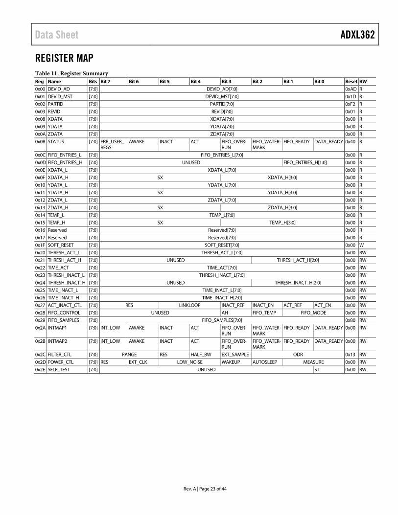
REGISTER MAP Table 11. Register Summary Reg Name Bits Bit 7 Bit 6 Bit 5 Bit 4 Bit 3 Bit 2 Bit 1 Bit 0 Reset RW
0x00 DEVID_AD [7:0] DEVID_AD[7:0] 0xAD R
0x01 DEVID_MST [7:0] DEVID_MST[7:0] 0x1D R
0x02 PARTID [7:0] PARTID[7:0] 0xF2 R
0x03 REVID [7:0] REVID[7:0] 0x01 R
0x08 XDATA [7:0] XDATA[7:0] 0x00 R
0x09 YDATA [7:0] YDATA[7:0] 0x00 R
0x0A ZDATA [7:0] ZDATA[7:0] 0x00 R
0x0B STATUS [7:0] ERR_USER_ REGS
AWAKE INACT ACT FIFO_OVER-RUN
FIFO_WATER-MARK
FIFO_READY DATA_READY 0x40 R
0x0C FIFO_ENTRIES_L [7:0] FIFO_ENTRIES_L[7:0] 0x00 R
0x0D FIFO_ENTRIES_H [7:0] UNUSED FIFO_ENTRIES_H[1:0] 0x00 R
0x0E XDATA_L [7:0] XDATA_L[7:0] 0x00 R
0x0F XDATA_H [7:0] SX XDATA_H[3:0] 0x00 R
0x10 YDATA_L [7:0] YDATA_L[7:0] 0x00 R
0x11 YDATA_H [7:0] SX YDATA_H[3:0] 0x00 R
0x12 ZDATA_L [7:0] ZDATA_L[7:0] 0x00 R
0x13 ZDATA_H [7:0] SX ZDATA_H[3:0] 0x00 R
0x14 TEMP_L [7:0] TEMP_L[7:0] 0x00 R
0x15 TEMP_H [7:0] SX TEMP_H[3:0] 0x00 R
0x16 Reserved [7:0] Reserved[7:0] 0x00 R
0x17 Reserved [7:0] Reserved[7:0] 0x00 R
0x1F SOFT_RESET [7:0] SOFT_RESET[7:0] 0x00 W
0x20 THRESH_ACT_L [7:0] THRESH_ACT_L[7:0] 0x00 RW
0x21 THRESH_ACT_H [7:0] UNUSED THRESH_ACT_H[2:0] 0x00 RW
0x22 TIME_ACT [7:0] TIME_ACT[7:0] 0x00 RW
0x23 THRESH_INACT_L [7:0] THRESH_INACT_L[7:0] 0x00 RW
0x24 THRESH_INACT_H [7:0] UNUSED THRESH_INACT_H[2:0] 0x00 RW
0x25 TIME_INACT_L [7:0] TIME_INACT_L[7:0] 0x00 RW
0x26 TIME_INACT_H [7:0] TIME_INACT_H[7:0] 0x00 RW
0x27 ACT_INACT_CTL [7:0] RES LINKLOOP INACT_REF INACT_EN ACT_REF ACT_EN 0x00 RW
0x28 FIFO_CONTROL [7:0] UNUSED AH FIFO_TEMP FIFO_MODE 0x00 RW
0x29 FIFO_SAMPLES [7:0] FIFO_SAMPLES[7:0] 0x80 RW
0x2A INTMAP1 [7:0] INT_LOW AWAKE INACT ACT FIFO_OVER-RUN
FIFO_WATER-MARK
FIFO_READY DATA_READY 0x00 RW
0x2B INTMAP2 [7:0] INT_LOW AWAKE INACT ACT FIFO_OVER-RUN
FIFO_WATER-MARK
FIFO_READY DATA_READY 0x00 RW
0x2C FILTER_CTL [7:0] RANGE RES HALF_BW EXT_SAMPLE ODR 0x13 RW
0x2D POWER_CTL [7:0] RES EXT_CLK LOW_NOISE WAKEUP AUTOSLEEP MEASURE 0x00 RW
0x2E SELF_TEST [7:0] UNUSED ST 0x00 RW
ADXL362 Data Sheet
Rev. A | Page 24 of 44
REGISTER DETAILS This section describes the functions of the ADXL362 registers. The ADXL362 powers up with default register values in the as shown in the Reset column of Table 11 in the Register Map section.
Note that any changes to the registers before the POWER_CTL register (Register 0x00 to Register 0x2C) should be made with the device in standby. If changes are made while the ADXL362 is in measurement mode, they may be effective for only part of a measurement.
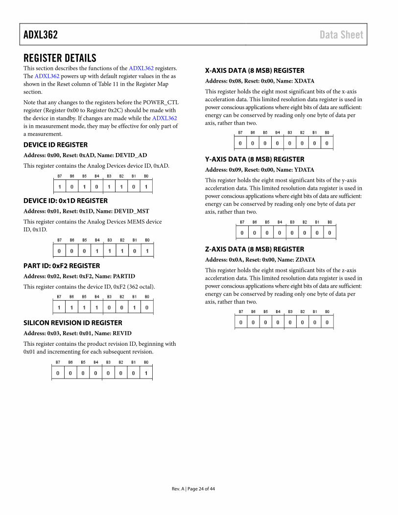
DEVICE ID REGISTER Address: 0x00, Reset: 0xAD, Name: DEVID_AD
This register contains the Analog Devices device ID, 0xAD.
DEVICE ID: 0x1D REGISTER Address: 0x01, Reset: 0x1D, Name: DEVID_MST
This register contains the Analog Devices MEMS device ID, 0x1D.
PART ID: 0xF2 REGISTER Address: 0x02, Reset: 0xF2, Name: PARTID
This register contains the device ID, 0xF2 (362 octal).
SILICON REVISION ID REGISTER Address: 0x03, Reset: 0x01, Name: REVID
This register contains the product revision ID, beginning with 0x01 and incrementing for each subsequent revision.
X-AXIS DATA (8 MSB) REGISTER Address: 0x08, Reset: 0x00, Name: XDATA
This register holds the eight most significant bits of the x-axis acceleration data. This limited resolution data register is used in power conscious applications where eight bits of data are sufficient: energy can be conserved by reading only one byte of data per axis, rather than two.
Y-AXIS DATA (8 MSB) REGISTER Address: 0x09, Reset: 0x00, Name: YDATA
This register holds the eight most significant bits of the y-axis acceleration data. This limited resolution data register is used in power conscious applications where eight bits of data are sufficient: energy can be conserved by reading only one byte of data per axis, rather than two.
Z-AXIS DATA (8 MSB) REGISTER Address: 0x0A, Reset: 0x00, Name: ZDATA
This register holds the eight most significant bits of the z-axis acceleration data. This limited resolution data register is used in power conscious applications where eight bits of data are sufficient: energy can be conserved by reading only one byte of data per axis, rather than two.
Data Sheet ADXL362
Rev. A | Page 25 of 44
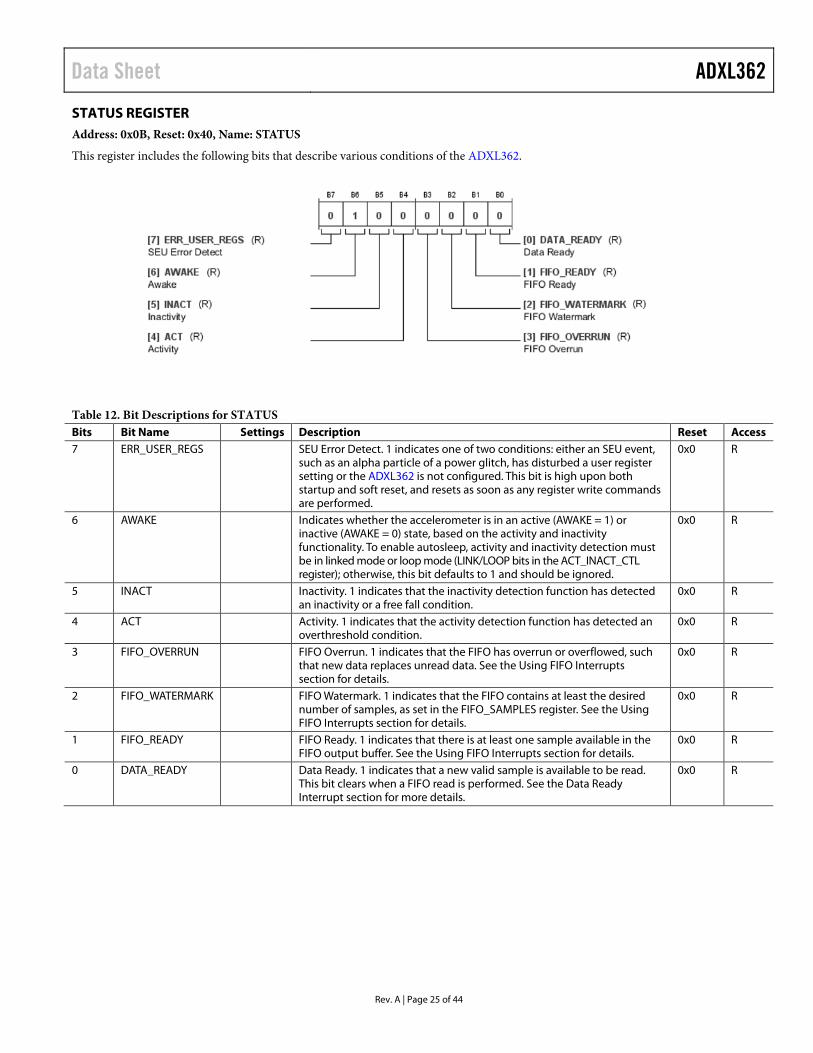
STATUS REGISTER Address: 0x0B, Reset: 0x40, Name: STATUS
This register includes the following bits that describe various conditions of the ADXL362.
Table 12. Bit Descriptions for STATUS Bits Bit Name Settings Description Reset Access 7 ERR_USER_REGS SEU Error Detect. 1 indicates one of two conditions: either an SEU event,
such as an alpha particle of a power glitch, has disturbed a user register setting or the ADXL362 is not configured. This bit is high upon both startup and soft reset, and resets as soon as any register write commands are performed.
0x0 R
6 AWAKE Indicates whether the accelerometer is in an active (AWAKE = 1) or inactive (AWAKE = 0) state, based on the activity and inactivity functionality. To enable autosleep, activity and inactivity detection must be in linked mode or loop mode (LINK/LOOP bits in the ACT_INACT_CTL register); otherwise, this bit defaults to 1 and should be ignored.
0x0 R
5 INACT Inactivity. 1 indicates that the inactivity detection function has detected an inactivity or a free fall condition.
0x0 R
4 ACT Activity. 1 indicates that the activity detection function has detected an overthreshold condition.
0x0 R
3 FIFO_OVERRUN FIFO Overrun. 1 indicates that the FIFO has overrun or overflowed, such that new data replaces unread data. See the Using FIFO Interrupts section for details.
0x0 R
2 FIFO_WATERMARK FIFO Watermark. 1 indicates that the FIFO contains at least the desired number of samples, as set in the FIFO_SAMPLES register. See the Using FIFO Interrupts section for details.
0x0 R
1 FIFO_READY FIFO Ready. 1 indicates that there is at least one sample available in the FIFO output buffer. See the Using FIFO Interrupts section for details.
0x0 R
0 DATA_READY Data Ready. 1 indicates that a new valid sample is available to be read. This bit clears when a FIFO read is performed. See the Data Ready Interrupt section for more details.
0x0 R
ADXL362 Data Sheet
Rev. A | Page 26 of 44
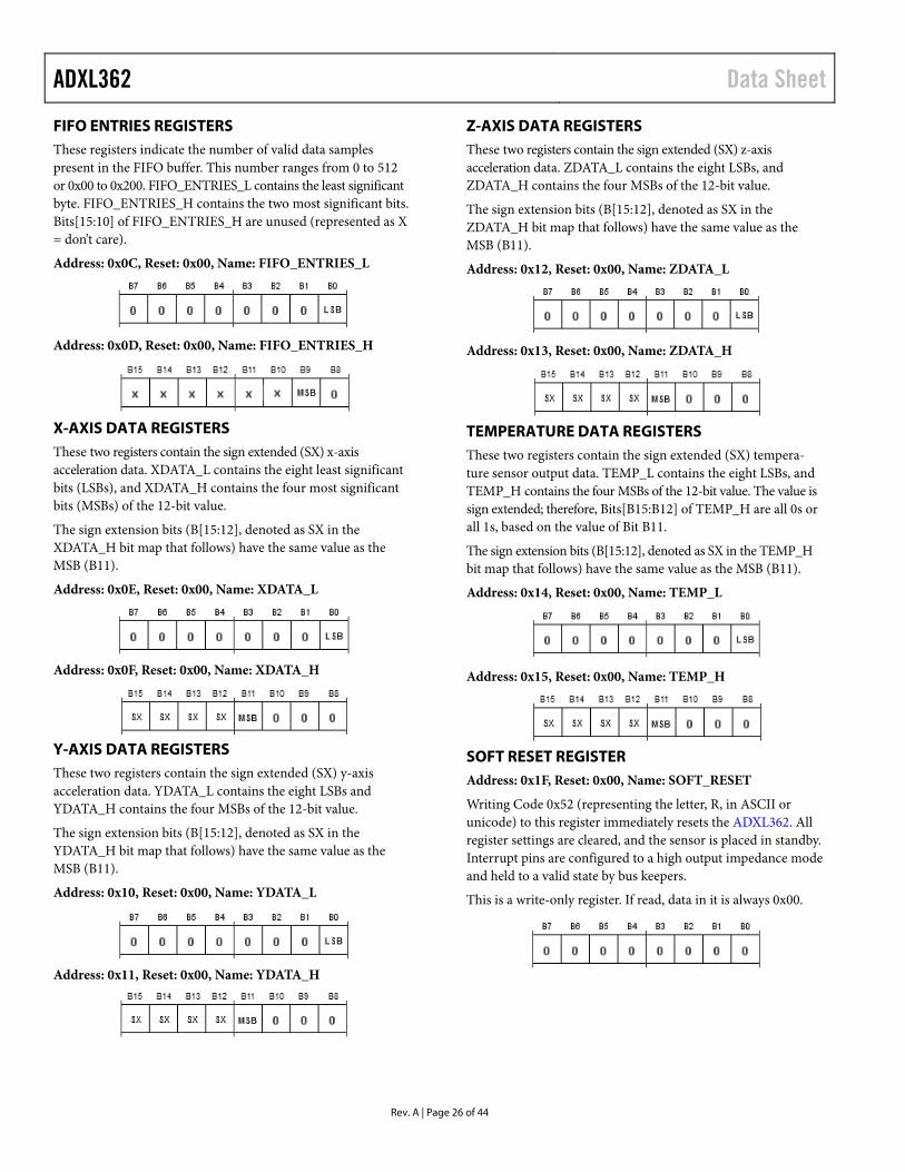
FIFO ENTRIES REGISTERS These registers indicate the number of valid data samples present in the FIFO buffer. This number ranges from 0 to 512 or 0x00 to 0x200. FIFO_ENTRIES_L contains the least significant byte. FIFO_ENTRIES_H contains the two most significant bits. Bits[15:10] of FIFO_ENTRIES_H are unused (represented as X = don’t care).
Address: 0x0C, Reset: 0x00, Name: FIFO_ENTRIES_L
Address: 0x0D, Reset: 0x00, Name: FIFO_ENTRIES_H
X-AXIS DATA REGISTERS These two registers contain the sign extended (SX) x-axis acceleration data. XDATA_L contains the eight least significant bits (LSBs), and XDATA_H contains the four most significant bits (MSBs) of the 12-bit value.
The sign extension bits (B[15:12], denoted as SX in the XDATA_H bit map that follows) have the same value as the MSB (B11).
Address: 0x0E, Reset: 0x00, Name: XDATA_L
Address: 0x0F, Reset: 0x00, Name: XDATA_H
Y-AXIS DATA REGISTERS These two registers contain the sign extended (SX) y-axis acceleration data. YDATA_L contains the eight LSBs and YDATA_H contains the four MSBs of the 12-bit value.
The sign extension bits (B[15:12], denoted as SX in the YDATA_H bit map that follows) have the same value as the MSB (B11).
Address: 0x10, Reset: 0x00, Name: YDATA_L
Address: 0x11, Reset: 0x00, Name: YDATA_H
Z-AXIS DATA REGISTERS These two registers contain the sign extended (SX) z-axis acceleration data. ZDATA_L contains the eight LSBs, and ZDATA_H contains the four MSBs of the 12-bit value.
The sign extension bits (B[15:12], denoted as SX in the ZDATA_H bit map that follows) have the same value as the MSB (B11).
Address: 0x12, Reset: 0x00, Name: ZDATA_L
Address: 0x13, Reset: 0x00, Name: ZDATA_H
TEMPERATURE DATA REGISTERS These two registers contain the sign extended (SX) tempera-ture sensor output data. TEMP_L contains the eight LSBs, and TEMP_H contains the four MSBs of the 12-bit value. The value is sign extended; therefore, Bits[B15:B12] of TEMP_H are all 0s or all 1s, based on the value of Bit B11.
The sign extension bits (B[15:12], denoted as SX in the TEMP_H bit map that follows) have the same value as the MSB (B11).
Address: 0x14, Reset: 0x00, Name: TEMP_L
Address: 0x15, Reset: 0x00, Name: TEMP_H
SOFT RESET REGISTER Address: 0x1F, Reset: 0x00, Name: SOFT_RESET
Writing Code 0x52 (representing the letter, R, in ASCII or unicode) to this register immediately resets the ADXL362. All register settings are cleared, and the sensor is placed in standby. Interrupt pins are configured to a high output impedance mode and held to a valid state by bus keepers.
This is a write-only register. If read, data in it is always 0x00.
Data Sheet ADXL362
Rev. A | Page 27 of 44
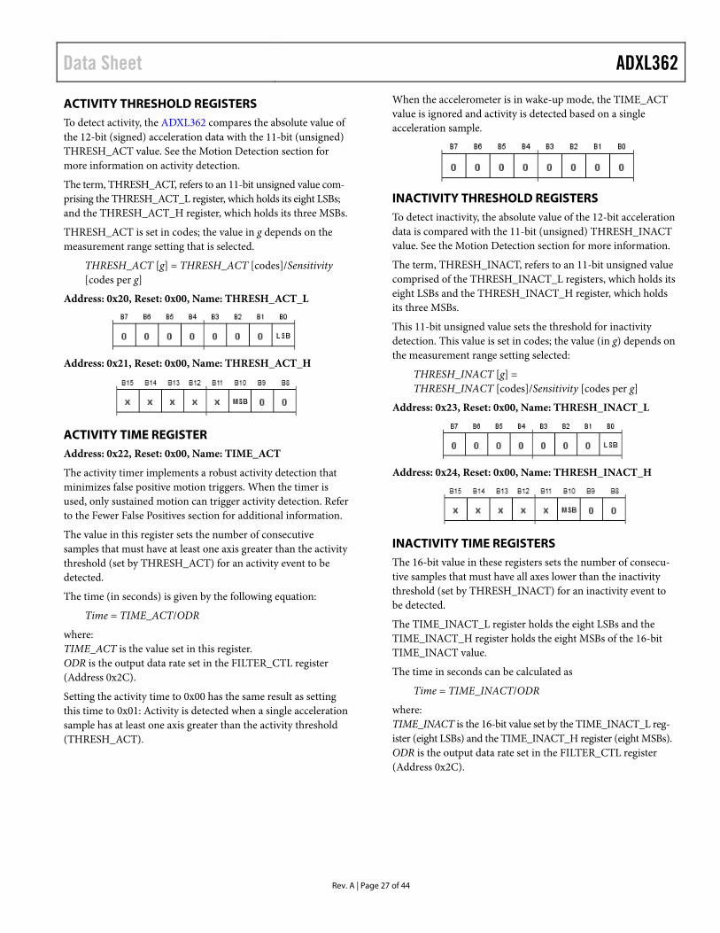
ACTIVITY THRESHOLD REGISTERS To detect activity, the ADXL362 compares the absolute value of the 12-bit (signed) acceleration data with the 11-bit (unsigned) THRESH_ACT value. See the Motion Detection section for more information on activity detection.
The term, THRESH_ACT, refers to an 11-bit unsigned value com-prising the THRESH_ACT_L register, which holds its eight LSBs; and the THRESH_ACT_H register, which holds its three MSBs.
THRESH_ACT is set in codes; the value in g depends on the measurement range setting that is selected.
THRESH_ACT [g] = THRESH_ACT [codes]/Sensitivity [codes per g]
Address: 0x20, Reset: 0x00, Name: THRESH_ACT_L
Address: 0x21, Reset: 0x00, Name: THRESH_ACT_H
ACTIVITY TIME REGISTER Address: 0x22, Reset: 0x00, Name: TIME_ACT
The activity timer implements a robust activity detection that minimizes false positive motion triggers. When the timer is used, only sustained motion can trigger activity detection. Refer to the Fewer False Positives section for additional information.
The value in this register sets the number of consecutive samples that must have at least one axis greater than the activity threshold (set by THRESH_ACT) for an activity event to be detected.
The time (in seconds) is given by the following equation:
Time = TIME_ACT/ODR
where: TIME_ACT is the value set in this register. ODR is the output data rate set in the FILTER_CTL register (Address 0x2C).
Setting the activity time to 0x00 has the same result as setting this time to 0x01: Activity is detected when a single acceleration sample has at least one axis greater than the activity threshold (THRESH_ACT).
When the accelerometer is in wake-up mode, the TIME_ACT value is ignored and activity is detected based on a single acceleration sample.
INACTIVITY THRESHOLD REGISTERS To detect inactivity, the absolute value of the 12-bit acceleration data is compared with the 11-bit (unsigned) THRESH_INACT value. See the Motion Detection section for more information.
The term, THRESH_INACT, refers to an 11-bit unsigned value comprised of the THRESH_INACT_L registers, which holds its eight LSBs and the THRESH_INACT_H register, which holds its three MSBs.
This 11-bit unsigned value sets the threshold for inactivity detection. This value is set in codes; the value (in g) depends on the measurement range setting selected:
THRESH_INACT [g] = THRESH_INACT [codes]/Sensitivity [codes per g]
Address: 0x23, Reset: 0x00, Name: THRESH_INACT_L
Address: 0x24, Reset: 0x00, Name: THRESH_INACT_H
INACTIVITY TIME REGISTERS The 16-bit value in these registers sets the number of consecu-tive samples that must have all axes lower than the inactivity threshold (set by THRESH_INACT) for an inactivity event to be detected.
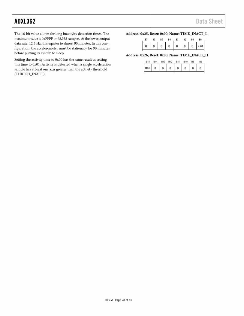
The TIME_INACT_L register holds the eight LSBs and the TIME_INACT_H register holds the eight MSBs of the 16-bit TIME_INACT value.
The time in seconds can be calculated as
Time = TIME_INACT/ODR
where: TIME_INACT is the 16-bit value set by the TIME_INACT_L reg-ister (eight LSBs) and the TIME_INACT_H register (eight MSBs). ODR is the output data rate set in the FILTER_CTL register (Address 0x2C).
ADXL362 Data Sheet
Rev. A | Page 28 of 44
The 16-bit value allows for long inactivity detection times. The maximum value is 0xFFFF or 65,535 samples. At the lowest output data rate, 12.5 Hz, this equates to almost 90 minutes. In this con-figuration, the accelerometer must be stationary for 90 minutes before putting its system to sleep.
Setting the activity time to 0x00 has the same result as setting this time to 0x01: Activity is detected when a single acceleration sample has at least one axis greater than the activity threshold (THRESH_INACT).
Address: 0x25, Reset: 0x00, Name: TIME_INACT_L
Address: 0x26, Reset: 0x00, Name: TIME_INACT_H
Data Sheet ADXL362
Rev. A | Page 29 of 44
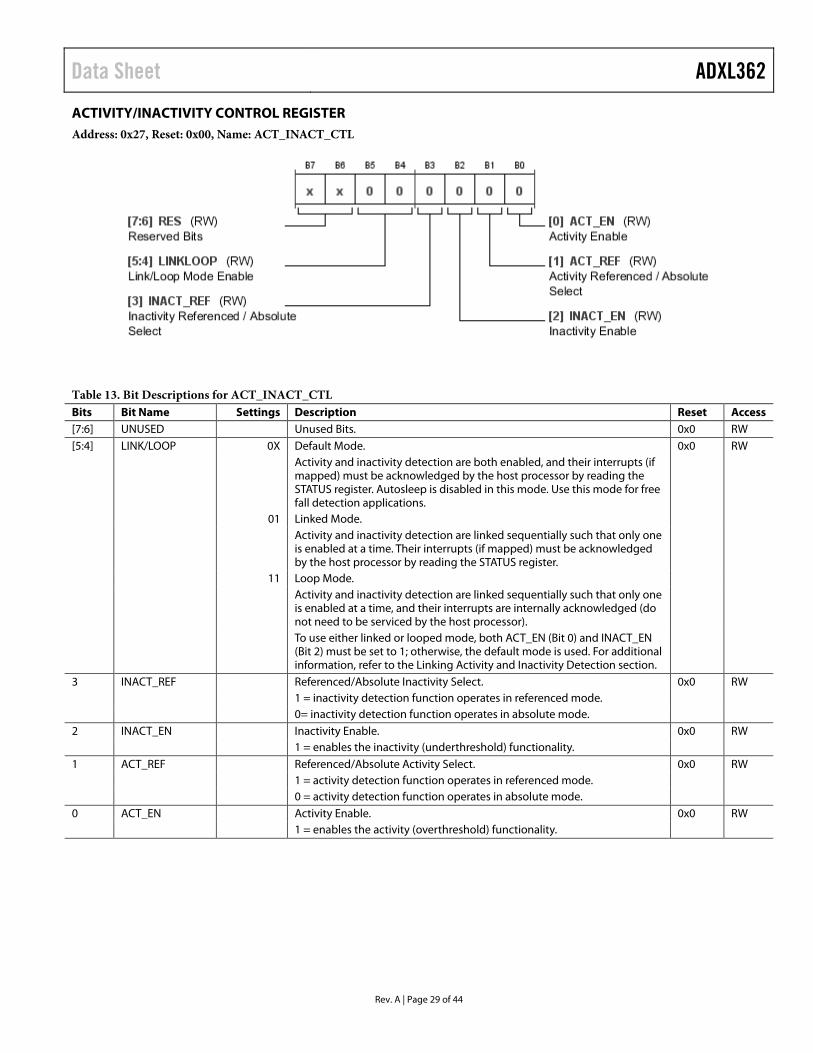
ACTIVITY/INACTIVITY CONTROL REGISTER Address: 0x27, Reset: 0x00, Name: ACT_INACT_CTL
Table 13. Bit Descriptions for ACT_INACT_CTL Bits Bit Name Settings Description Reset Access [7:6] UNUSED Unused Bits. 0x0 RW [5:4] LINK/LOOP 0X Default Mode. 0x0 RW
Activity and inactivity detection are both enabled, and their interrupts (if mapped) must be acknowledged by the host processor by reading the STATUS register. Autosleep is disabled in this mode. Use this mode for free fall detection applications.
01 Linked Mode. Activity and inactivity detection are linked sequentially such that only one is enabled at a time. Their interrupts (if mapped) must be acknowledged by the host processor by reading the STATUS register.
11 Loop Mode. Activity and inactivity detection are linked sequentially such that only one is enabled at a time, and their interrupts are internally acknowledged (do not need to be serviced by the host processor).
To use either linked or looped mode, both ACT_EN (Bit 0) and INACT_EN (Bit 2) must be set to 1; otherwise, the default mode is used. For additional information, refer to the Linking Activity and Inactivity Detection section.
3 INACT_REF Referenced/Absolute Inactivity Select. 0x0 RW 1 = inactivity detection function operates in referenced mode. 0= inactivity detection function operates in absolute mode.
2 INACT_EN Inactivity Enable. 0x0 RW 1 = enables the inactivity (underthreshold) functionality.
1 ACT_REF Referenced/Absolute Activity Select. 0x0 RW 1 = activity detection function operates in referenced mode. 0 = activity detection function operates in absolute mode.
0 ACT_EN Activity Enable. 0x0 RW 1 = enables the activity (overthreshold) functionality.
ADXL362 Data Sheet
Rev. A | Page 30 of 44
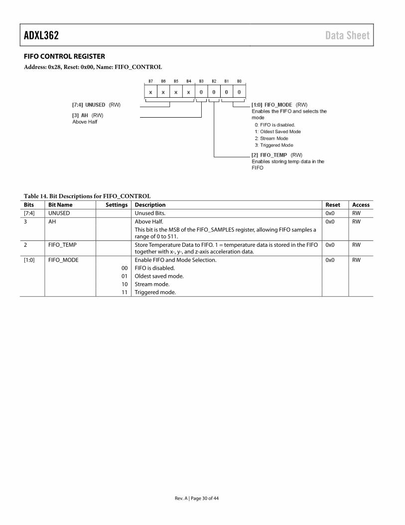
FIFO CONTROL REGISTER Address: 0x28, Reset: 0x00, Name: FIFO_CONTROL
Table 14. Bit Descriptions for FIFO_CONTROL Bits Bit Name Settings Description Reset Access [7:4] UNUSED Unused Bits. 0x0 RW 3 AH Above Half. 0x0 RW
This bit is the MSB of the FIFO_SAMPLES register, allowing FIFO samples a range of 0 to 511.
2 FIFO_TEMP Store Temperature Data to FIFO. 1 = temperature data is stored in the FIFO together with x-, y-, and z-axis acceleration data.
0x0 RW
[1:0] FIFO_MODE Enable FIFO and Mode Selection. 0x0 RW 00 FIFO is disabled. 01 Oldest saved mode. 10 Stream mode. 11 Triggered mode.
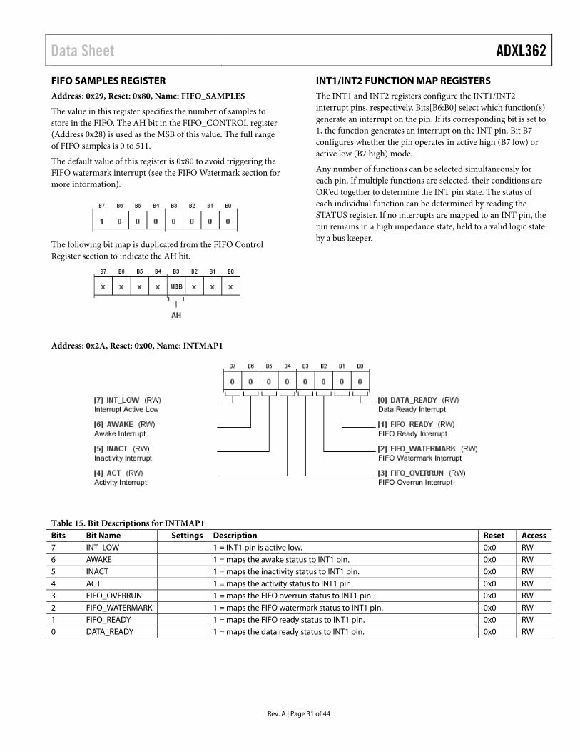
Data Sheet ADXL362
Rev. A | Page 31 of 44
FIFO SAMPLES REGISTER Address: 0x29, Reset: 0x80, Name: FIFO_SAMPLES
The value in this register specifies the number of samples to store in the FIFO. The AH bit in the FIFO_CONTROL register (Address 0x28) is used as the MSB of this value. The full range of FIFO samples is 0 to 511.
The default value of this register is 0x80 to avoid triggering the FIFO watermark interrupt (see the FIFO Watermark section for more information).
The following bit map is duplicated from the FIFO Control Register section to indicate the AH bit.
INT1/INT2 FUNCTION MAP REGISTERS The INT1 and INT2 registers configure the INT1/INT2 interrupt pins, respectively. Bits[B6:B0] select which function(s) generate an interrupt on the pin. If its corresponding bit is set to 1, the function generates an interrupt on the INT pin. Bit B7 configures whether the pin operates in active high (B7 low) or active low (B7 high) mode.
Any number of functions can be selected simultaneously for each pin. If multiple functions are selected, their conditions are OR'ed together to determine the INT pin state. The status of each individual function can be determined by reading the STATUS register. If no interrupts are mapped to an INT pin, the pin remains in a high impedance state, held to a valid logic state by a bus keeper.
Address: 0x2A, Reset: 0x00, Name: INTMAP1
Table 15. Bit Descriptions for INTMAP1 Bits Bit Name Settings Description Reset Access 7 INT_LOW 1 = INT1 pin is active low. 0x0 RW 6 AWAKE 1 = maps the awake status to INT1 pin. 0x0 RW 5 INACT 1 = maps the inactivity status to INT1 pin. 0x0 RW 4 ACT 1 = maps the activity status to INT1 pin. 0x0 RW 3 FIFO_OVERRUN 1 = maps the FIFO overrun status to INT1 pin. 0x0 RW 2 FIFO_WATERMARK 1 = maps the FIFO watermark status to INT1 pin. 0x0 RW 1 FIFO_READY 1 = maps the FIFO ready status to INT1 pin. 0x0 RW 0 DATA_READY 1 = maps the data ready status to INT1 pin. 0x0 RW
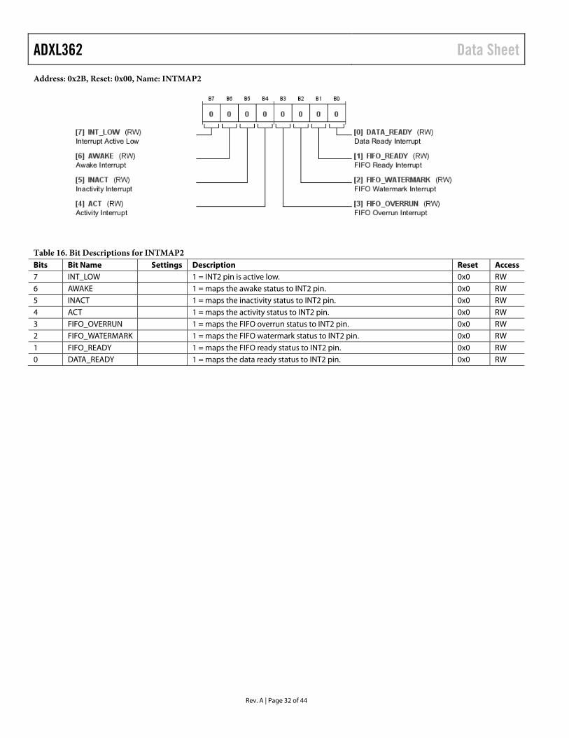
ADXL362 Data Sheet
Rev. A | Page 32 of 44
Address: 0x2B, Reset: 0x00, Name: INTMAP2
Table 16. Bit Descriptions for INTMAP2 Bits Bit Name Settings Description Reset Access 7 INT_LOW 1 = INT2 pin is active low. 0x0 RW 6 AWAKE 1 = maps the awake status to INT2 pin. 0x0 RW 5 INACT 1 = maps the inactivity status to INT2 pin. 0x0 RW 4 ACT 1 = maps the activity status to INT2 pin. 0x0 RW 3 FIFO_OVERRUN 1 = maps the FIFO overrun status to INT2 pin. 0x0 RW 2 FIFO_WATERMARK 1 = maps the FIFO watermark status to INT2 pin. 0x0 RW 1 FIFO_READY 1 = maps the FIFO ready status to INT2 pin. 0x0 RW 0 DATA_READY 1 = maps the data ready status to INT2 pin. 0x0 RW
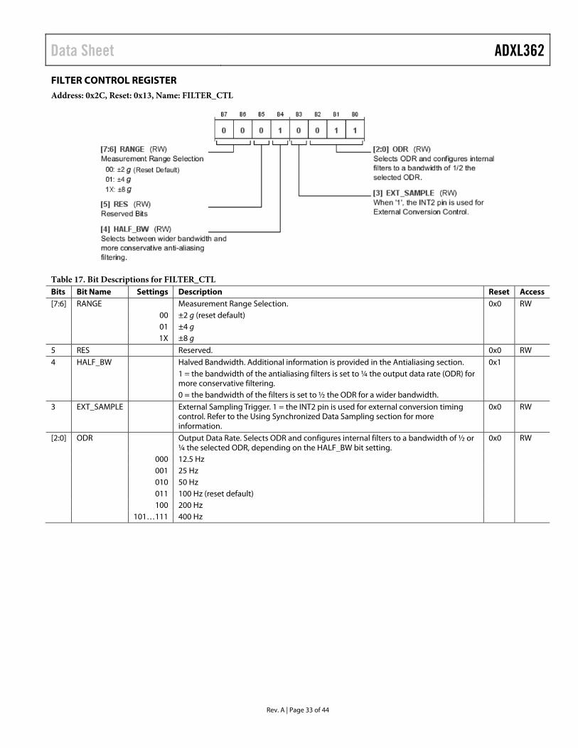
Data Sheet ADXL362
Rev. A | Page 33 of 44
FILTER CONTROL REGISTER Address: 0x2C, Reset: 0x13, Name: FILTER_CTL
Table 17. Bit Descriptions for FILTER_CTL Bits Bit Name Settings Description Reset Access [7:6] RANGE Measurement Range Selection. 0x0 RW 00 ±2 g (reset default) 01 ±4 g 1X ±8 g 5 RES Reserved. 0x0 RW 4 HALF_BW Halved Bandwidth. Additional information is provided in the Antialiasing section. 0x1
1 = the bandwidth of the antialiasing filters is set to ¼ the output data rate (ODR) for more conservative filtering. 0 = the bandwidth of the filters is set to ½ the ODR for a wider bandwidth.
3 EXT_SAMPLE External Sampling Trigger. 1 = the INT2 pin is used for external conversion timing control. Refer to the Using Synchronized Data Sampling section for more information.
0x0 RW
[2:0] ODR Output Data Rate. Selects ODR and configures internal filters to a bandwidth of ½ or ¼ the selected ODR, depending on the HALF_BW bit setting.
0x0 RW
000 12.5 Hz 001 25 Hz 010 50 Hz 011 100 Hz (reset default) 100 200 Hz 101…111 400 Hz
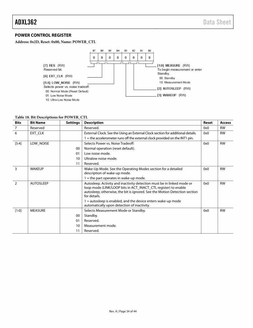
ADXL362 Data Sheet
Rev. A | Page 34 of 44
POWER CONTROL REGISTER Address: 0x2D, Reset: 0x00, Name: POWER_CTL
Table 18. Bit Descriptions for POWER_CTL Bits Bit Name Settings Description Reset Access 7 Reserved Reserved. 0x0 RW 6 EXT_CLK External Clock. See the Using an External Clock section for additional details. 0x0 RW
1 = the accelerometer runs off the external clock provided on the INT1 pin. [5:4] LOW_NOISE Selects Power vs. Noise Tradeoff: 0x0 RW 00 Normal operation (reset default). 01 Low noise mode. 10 Ultralow noise mode. 11 Reserved. 3 WAKEUP Wake-Up Mode. See the Operating Modes section for a detailed
description of wake-up mode. 0x0 RW
1 = the part operates in wake-up mode. 2 AUTOSLEEP Autosleep. Activity and inactivity detection must be in linked mode or
loop mode (LINK/LOOP bits in ACT_INACT_CTL register) to enable autosleep; otherwise, the bit is ignored. See the Motion Detection section for details.
0x0 RW
1 = autosleep is enabled, and the device enters wake-up mode automatically upon detection of inactivity.
[1:0] MEASURE Selects Measurement Mode or Standby. 0x0 RW 00 Standby. 01 Reserved. 10 Measurement mode. 11 Reserved.
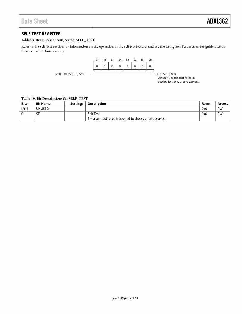
Data Sheet ADXL362
Rev. A | Page 35 of 44
SELF TEST REGISTER Address: 0x2E, Reset: 0x00, Name: SELF_TEST
Refer to the Self Test section for information on the operation of the self test feature, and see the Using Self Test section for guidelines on how to use this functionality.
Table 19. Bit Descriptions for SELF_TEST Bits Bit Name Settings Description Reset Access [7:1] UNUSED 0x0 RW 0 ST Self Test. 0x0 RW
1 = a self test force is applied to the x-, y-, and z-axes.
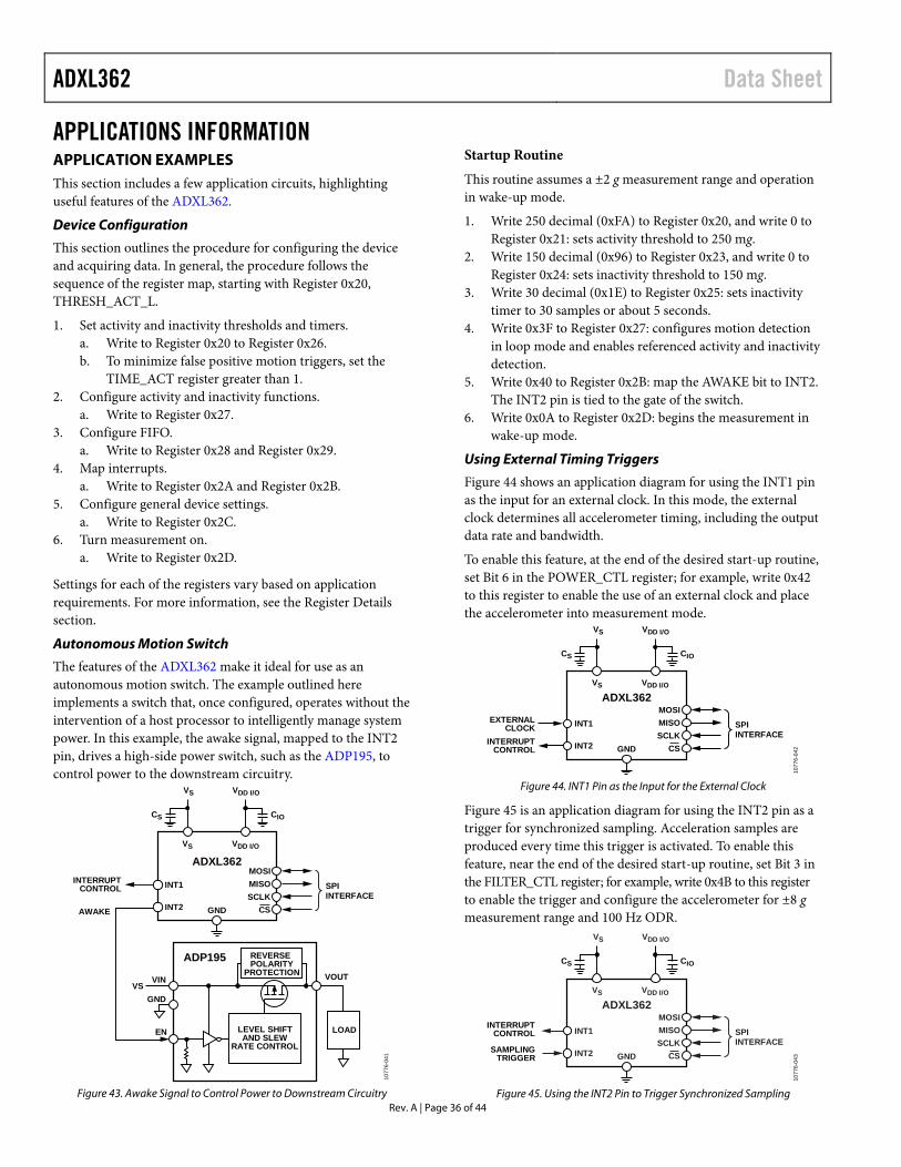
ADXL362 Data Sheet
Rev. A | Page 36 of 44
APPLICATIONS INFORMATION APPLICATION EXAMPLES This section includes a few application circuits, highlighting useful features of the ADXL362.
Device Configuration
This section outlines the procedure for configuring the device and acquiring data. In general, the procedure follows the sequence of the register map, starting with Register 0x20, THRESH_ACT_L.
1. Set activity and inactivity thresholds and timers. a. Write to Register 0x20 to Register 0x26. b. To minimize false positive motion triggers, set the
TIME_ACT register greater than 1. 2. Configure activity and inactivity functions.
a. Write to Register 0x27. 3. Configure FIFO.
a. Write to Register 0x28 and Register 0x29. 4. Map interrupts.
a. Write to Register 0x2A and Register 0x2B. 5. Configure general device settings.
a. Write to Register 0x2C. 6. Turn measurement on.
a. Write to Register 0x2D.
Settings for each of the registers vary based on application requirements. For more information, see the Register Details section.
Autonomous Motion Switch
The features of the ADXL362 make it ideal for use as an autonomous motion switch. The example outlined here implements a switch that, once configured, operates without the intervention of a host processor to intelligently manage system power. In this example, the awake signal, mapped to the INT2 pin, drives a high-side power switch, such as the ADP195, to control power to the downstream circuitry.
ADXL362
GND
INT1
INT2 CSSCLKMISOMOSI
SPIINTERFACE
VS
VS
CS
VDD I/O
VDD I/O
CIO
INTERRUPTCONTROL
AWAKE
GND
EN
VINVS
LOAD
VOUT
ADP195
LEVEL SHIFTAND SLEW
RATE CONTROL
REVERSEPOLARITY
PROTECTION
1077
6-04
1
Figure 43. Awake Signal to Control Power to Downstream Circuitry
Startup Routine
This routine assumes a ±2 g measurement range and operation in wake-up mode.
1. Write 250 decimal (0xFA) to Register 0x20, and write 0 to Register 0x21: sets activity threshold to 250 mg.
2. Write 150 decimal (0x96) to Register 0x23, and write 0 to Register 0x24: sets inactivity threshold to 150 mg.
3. Write 30 decimal (0x1E) to Register 0x25: sets inactivity timer to 30 samples or about 5 seconds.
4. Write 0x3F to Register 0x27: configures motion detection in loop mode and enables referenced activity and inactivity detection.
5. Write 0x40 to Register 0x2B: map the AWAKE bit to INT2. The INT2 pin is tied to the gate of the switch.
6. Write 0x0A to Register 0x2D: begins the measurement in wake-up mode.
Using External Timing Triggers
Figure 44 shows an application diagram for using the INT1 pin as the input for an external clock. In this mode, the external clock determines all accelerometer timing, including the output data rate and bandwidth.
To enable this feature, at the end of the desired start-up routine, set Bit 6 in the POWER_CTL register; for example, write 0x42 to this register to enable the use of an external clock and place the accelerometer into measurement mode.
ADXL362
GND
INT1
INT2 CSSCLKMISOMOSI
SPIINTERFACE
VS
VS
CS
VDD I/O
VDD I/O
CIO
INTERRUPTCONTROL
EXTERNALCLOCK
1077
6-04
2
Figure 44. INT1 Pin as the Input for the External Clock
Figure 45 is an application diagram for using the INT2 pin as a trigger for synchronized sampling. Acceleration samples are produced every time this trigger is activated. To enable this feature, near the end of the desired start-up routine, set Bit 3 in the FILTER_CTL register; for example, write 0x4B to this register to enable the trigger and configure the accelerometer for ±8 g measurement range and 100 Hz ODR.
ADXL362
GND
INT1
INT2 CSSCLKMISOMOSI
SPIINTERFACE
VS
VS
CS
VDD I/O
VDD I/O
CIO
INTERRUPTCONTROL
SAMPLINGTRIGGER
1077
6-04
3
Figure 45. Using the INT2 Pin to Trigger Synchronized Sampling
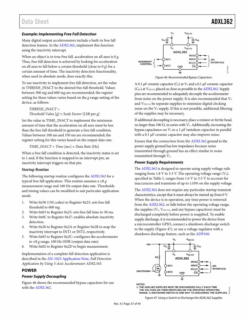
Data Sheet ADXL362
Rev. A | Page 37 of 44
Example: Implementing Free Fall Detection
Many digital output accelerometers include a built-in free fall detection feature. In the ADXL362, implement this function using the inactivity interrupt.
When an object is in true free fall, acceleration on all axes is 0 g. Thus, free fall detection is achieved by looking for acceleration on all axes to fall below a certain threshold (close to 0 g) for a certain amount of time. The inactivity detection functionality, when used in absolute mode, does exactly this.
To use inactivity to implement free fall detection, set the value in THRESH_INACT to the desired free fall threshold. Values between 300 mg and 600 mg are recommended; the register setting for these values varies based on the g range setting of the device, as follows:
THRESH_INACT = Threshold Value [g] × Scale Factor [LSB per g]
Set the value in TIME_INACT to implement the minimum amount of time that the acceleration on all axes must be less than the free fall threshold to generate a free fall condition. Values between 100 ms and 350 ms are recommended; the register setting for this varies based on the output data rate.
TIME_INACT = Time [sec] × Data Rate [Hz]
When a free fall condition is detected, the inactivity status is set to 1 and, if the function is mapped to an interrupt pin, an inactivity interrupt triggers on that pin.
Startup Routine
The following startup routine configures the ADXL362 for a typical free fall application. This routine assumes a ±8 g measurement range and 100 Hz output data rate. Thresholds and timing values can be modified to suit particular application needs.
1. Write 0x58 (150 codes) to Register 0x23: sets free fall threshold to 600 mg.
2. Write 0x03 to Register 0x25: sets free fall time to 30 ms. 3. Write 0x0C to Register 0x27: enables absolute inactivity
detection. 4. Write 0x20 to Register 0x2A or Register 0x2B to map the
inactivity interrupt to INT1 or INT2, respectively. 5. Write 0x83 to Register 0x2C: configures the accelerometer
to ±8 g range, 100 Hz ODR (output data rate). 6. Write 0x02 to Register 0x2D to begin measurement.
Implementation of a complete fall detection application is described in the AN-1023 Application Note, Fall Detection Application by Using 3-Axis Accelerometer ADXL345.
POWER Power Supply Decoupling
Figure 46 shows the recommended bypass capacitors for use with the ADXL362.
ADXL362
GND
INT1
INT2 CSSCLKMISOMOSI
SPIINTERFACE
VS
VS
CS
VDD I/O
VDD I/O
CIO
INTERRUPTCONTROL
1077
6-04
0
Figure 46. Recommended Bypass Capacitors
A 0.1 µF ceramic capacitor (CS) at VS and a 0.1 µF ceramic capacitor (CIO) at VDD I/O placed as close as possible to the ADXL362. Supply pins are recommended to adequately decouple the accelerometer from noise on the power supply. It is also recommended that VS and VDD I/O be separate supplies to minimize digital clocking noise on the VS supply. If this is not possible, additional filtering of the supplies may be necessary.
If additional decoupling is necessary, place a resistor or ferrite bead, no larger than 100 Ω, in series with VS. Additionally, increasing the bypass capacitance on VS to a 1 µF tantalum capacitor in parallel with a 0.1 µF ceramic capacitor may also improve noise.
Ensure that the connection from the ADXL362 ground to the power supply ground has low impedance because noise transmitted through ground has an effect similar to noise transmitted through VS.
Power Supply Requirements
The ADXL362 is designed to operate using supply voltage rails ranging from 1.8 V to 3.3 V. The operating voltage range (VS), specified in Table 1, ranges from 1.6 V to 3.5 V to account for inaccuracies and transients of up to ±10% on the supply voltage.
The ADXL362 does not require any particular startup transient characteristics, except that it must always be started up from 0 V. When the device is in operation, any time power is removed from the ADXL362, or falls below the operating voltage range, the supplies (VS, VDD I/O, and any bypass capacitors) must be discharged completely before power is reapplied. To enable supply discharge, it is recommended to power the device from a microcontroller GPIO, connect a shutdown discharge switch to the supply (Figure 47), or use a voltage regulator with a shutdown discharge feature, such as the ADP160.
ADXL362
GND
INT1
SHUTDOWN
NOTES1. THE ADXL362 SUPPLIES MUST BE DISCHARGED FULLY EACH TIME THE VOLTAGE ON THEM DROPS BELOW THE SPECIFIED OPERATING RANGE. A SHUTDOWN SWITCH IS ONE WAY TO DISCHARGE THE SUPPLIES.
VIN
R1
INT2 CSSCLKMISOMOSI
SPIINTERFACE
VS
VS
CS
VDD I/O
VDD I/O
CIO
1077
6-14
1
Figure 47. Using a Switch to Discharge the ADXL362 Supplies
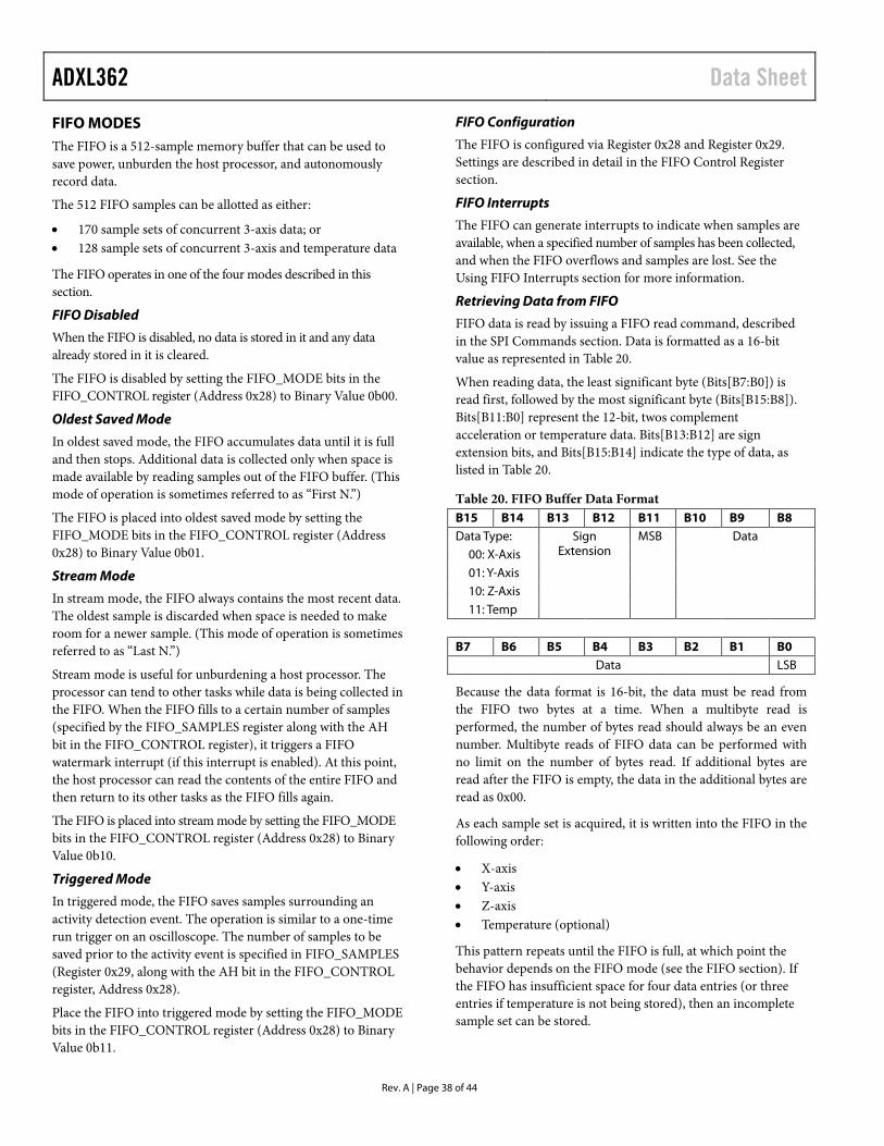
ADXL362 Data Sheet
Rev. A | Page 38 of 44
FIFO MODES The FIFO is a 512-sample memory buffer that can be used to save power, unburden the host processor, and autonomously record data.
The 512 FIFO samples can be allotted as either:
• 170 sample sets of concurrent 3-axis data; or • 128 sample sets of concurrent 3-axis and temperature data
The FIFO operates in one of the four modes described in this section.
FIFO Disabled
When the FIFO is disabled, no data is stored in it and any data already stored in it is cleared.
The FIFO is disabled by setting the FIFO_MODE bits in the FIFO_CONTROL register (Address 0x28) to Binary Value 0b00.
Oldest Saved Mode
In oldest saved mode, the FIFO accumulates data until it is full and then stops. Additional data is collected only when space is made available by reading samples out of the FIFO buffer. (This mode of operation is sometimes referred to as “First N.”)
The FIFO is placed into oldest saved mode by setting the FIFO_MODE bits in the FIFO_CONTROL register (Address 0x28) to Binary Value 0b01.
Stream Mode
In stream mode, the FIFO always contains the most recent data. The oldest sample is discarded when space is needed to make room for a newer sample. (This mode of operation is sometimes referred to as “Last N.”)
Stream mode is useful for unburdening a host processor. The processor can tend to other tasks while data is being collected in the FIFO. When the FIFO fills to a certain number of samples (specified by the FIFO_SAMPLES register along with the AH bit in the FIFO_CONTROL register), it triggers a FIFO watermark interrupt (if this interrupt is enabled). At this point, the host processor can read the contents of the entire FIFO and then return to its other tasks as the FIFO fills again.
The FIFO is placed into stream mode by setting the FIFO_MODE bits in the FIFO_CONTROL register (Address 0x28) to Binary Value 0b10.
Triggered Mode
In triggered mode, the FIFO saves samples surrounding an activity detection event. The operation is similar to a one-time run trigger on an oscilloscope. The number of samples to be saved prior to the activity event is specified in FIFO_SAMPLES (Register 0x29, along with the AH bit in the FIFO_CONTROL register, Address 0x28).
Place the FIFO into triggered mode by setting the FIFO_MODE bits in the FIFO_CONTROL register (Address 0x28) to Binary Value 0b11.
FIFO Configuration
The FIFO is configured via Register 0x28 and Register 0x29. Settings are described in detail in the FIFO Control Register section.
FIFO Interrupts
The FIFO can generate interrupts to indicate when samples are available, when a specified number of samples has been collected, and when the FIFO overflows and samples are lost. See the Using FIFO Interrupts section for more information.
Retrieving Data from FIFO
FIFO data is read by issuing a FIFO read command, described in the SPI Commands section. Data is formatted as a 16-bit value as represented in Table 20.
When reading data, the least significant byte (Bits[B7:B0]) is read first, followed by the most significant byte (Bits[B15:B8]). Bits[B11:B0] represent the 12-bit, twos complement acceleration or temperature data. Bits[B13:B12] are sign extension bits, and Bits[B15:B14] indicate the type of data, as listed in Table 20.
Table 20. FIFO Buffer Data Format B15 B14 B13 B12 B11 B10 B9 B8 Data Type: Sign
Extension MSB Data
00: X-Axis 01: Y-Axis 10: Z-Axis 11: Temp
B7 B6 B5 B4 B3 B2 B1 B0
Data LSB
Because the data format is 16-bit, the data must be read from the FIFO two bytes at a time. When a multibyte read is performed, the number of bytes read should always be an even number. Multibyte reads of FIFO data can be performed with no limit on the number of bytes read. If additional bytes are read after the FIFO is empty, the data in the additional bytes are read as 0x00.
As each sample set is acquired, it is written into the FIFO in the following order:
• X-axis • Y-axis • Z-axis • Temperature (optional)
This pattern repeats until the FIFO is full, at which point the behavior depends on the FIFO mode (see the FIFO section). If the FIFO has insufficient space for four data entries (or three entries if temperature is not being stored), then an incomplete sample set can be stored.
Data Sheet ADXL362
Rev. A | Page 39 of 44
FIFO data is output on a per datum basis. As each data item is read, the same amount of space is freed up in the stack. Again, this can lead to incomplete sample sets being present in the FIFO.
For additional system level FIFO applications, refer to the AN-1025 Application Note, Utilization of the First In, First Out (FIFO) Buffer in Analog Devices, Inc. Digital Accelerometers.
INTERRUPTS Several of the built-in functions of the ADXL362 can trigger interrupts to alert the host processor of certain status conditions. This section describes the functionality of these interrupts.
Interrupt Pins Interrupts can be mapped to either (or both) of two designated output pins, INT1 and INT2, by setting the appropriate bits in the INTMAP1 and INTMAP2 registers, respectively. All functions can be used simultaneously. If multiple interrupts are mapped to one pin, the OR combination of the interrupts determines the status of the pin. If no functions are mapped to an interrupt pin, that pin is automatically configured to a high impedance (high-Z) state. The pins are also placed in the high-Z state upon a reset.
When a certain status condition is detected, the pin that condition is mapped to is activated. The configuration of the pin is active high by default so that when it is activated, the pin goes high. However, this configuration can be switched to
active low by setting the INT_LOW bit in the appropriate INTMAPx register.
The INT pins can be connected to the interrupt input of a host processor where interrupts are responded to with an interrupt routine. Because multiple functions can be mapped to the same pin, the STATUS register can be used to determine which condition caused the interrupt to trigger.
Clear interrupts in one of several ways, as follows:
• Reading the STATUS register (Address 0x0B) clears activity and inactivity interrupts.
• Reading from the data registers. Address 0x08 to Address 0x0A or Address 0x0E to Address 0x15 clears the data ready interrupt.
• Reading enough data from the FIFO buffer so that interrupt conditions are no longer met clears the FIFO ready, FIFO watermark, and FIFO overrun interrupts.
Both interrupt pins are push-pull low impedance pins with an output impedance of about 500 Ω (typical) and digital output specifications, as shown in Table 21. Both pins have bus keepers that hold them to a valid logic state when they are in a high impedance mode. To prevent interrupts from being falsely triggered during configuration, disable interrupts while their settings, such as thresholds, timings, or other values, are configured.
Table 21. Interrupt Pin Digital Output Limit1 Parameter Test Conditions Min Max Unit Digital Output
Low Level Output Voltage (VOL) IOL = 500 µA 0.2 × VDD I/O V High Level Output Voltage (VOH) IOH = −300 µA 0.8 × VDD I/O V Low Level Output Current (IOL) VOL = VOL, max 500 µA High Level Output Current (IOH) VOH = VOH, min −300 µA
1 Limits based on design, not production tested.
ADXL362 Data Sheet
Rev. A | Page 40 of 44
Alternate Functions of Interrupt Pins
The INT1 and INT2 pins can be configured for use as input pins instead of for signaling interrupts. INT1 is used as an external clock input when the EXT_CLK bit (Bit 6) in the POWER_CTL register (Address 0x2D) is set. INT2 is used as the trigger input for synchronized sampling when the EXT_SAMPLE bit (Bit 3) in the FILTER_CTL register (Address 0x2C) is set. One or both of these alternate functions can be used concurrently; however, if an interrupt pin is used for its alternate function, it cannot simultaneously be used for its primary function, to signal interrupts.
External clocking and data synchronization are described in the Applications Information section.
Activity and Inactivity Interrupts
The ACT bit (Bit 4) and INACT bit (Bit 5) in the STATUS register are set when activity and inactivity are detected, respectively. Detection procedures and criteria are described in the Motion Detection section.
Data Ready Interrupt
The DATA_READY bit (Bit 0) is set when new valid data is available, and it is cleared when no new data is available.
The DATA_READY bit is not set while any of the data registers, Address 0x08 to Address 0x0A and Address 0x0E to Address 0x15, are being read. If DATA_READY = 0 prior to a register read and new data becomes available during the register read, DATA_READY remains at 0 until the read is complete and, only then, is set to 1.
If DATA_READY = 1 prior to a register read, it is cleared at the start of the register read.
If DATA_READY = 1 prior to a register read and new data becomes available during the register read, DATA_READY is cleared to 0 at the start of the register read and remains at 0 throughout the read. When the read is complete, DATA_READY is set to 1.
Using FIFO Interrupts
FIFO Watermark
The FIFO_WATERMARK bit (Bit 2) is set when the number of samples stored in the FIFO is equal to or exceeds the number speci-fied in the FIFO_SAMPLES register (Address 0x29) together with the AH bit in the FIFO_CONTROL register (Bit 3, Address 0x28). The FIFO_WATERMARK bit is cleared automatically when enough samples are read from the FIFO, such that the number of samples remaining is lower than that specified.
If the number of FIFO samples is set to 0, the FIFO watermark interrupt is set. To avoid unexpectedly triggering this interrupt, the default value of the FIFO_SAMPLES register is 0x80.
FIFO Ready
The FIFO_READY bit (Bit 1) is set when there is at least one valid sample available in the FIFO output buffer. This bit is cleared when no valid data is available in the FIFO.
Overrun
The FIFO_OVERRUN bit (Bit 3) is set when the FIFO has overrun or overflowed, such that new data replaces unread data. This may indicate a full FIFO that has not yet been emptied or a clocking error caused by a slow SPI transaction. If the FIFO is configured to oldest saved mode, an overrun event indicates that there is insufficient space available for a new sample.
The FIFO_OVERRUN bit is cleared automatically when the contents of the FIFO are read. Likewise, when the FIFO is disabled, the FIFO_OVERRUN bit is cleared.
USING SYNCHRONIZED DATA SAMPLING For applications that require a precisely timed acceleration measurement, the ADXL362 features an option to synchronize acceleration sampling to an external trigger. The EXT_SAMPLE bit (Bit 3) in the FILTER_CTL Register (Address 0x2C) enables this feature. When the EXT_SAMPLE bit is set to 1, the INT2 pin is automatically reconfigured for use as the sync trigger input.
When external triggering is enabled, it is up to the system designer to ensure that the sampling frequency meets system requirements. Sampling too infrequently causes aliasing. Noise can be lowered by oversampling; however, sampling at too high a frequency may not allow enough time for the accelerometer to process the acceleration data and convert it to valid digital output.
When Nyquist criteria are met, signal integrity is maintained. An internal antialiasing filter is available in the ADXL362 and can assist the system designer in maintaining signal integrity. To prevent aliasing, set the filter bandwidth to a frequency no greater than ½ the sampling rate. For example, when sampling at 100 Hz, set the filter pole to no higher than 50 Hz. The filter pole is set via the ODR bits in the FILTER_CTL register (Address 0x2C). The filter bandwidth is set to ½ the ODR and is set via these bits. Even though the ODR is ignored (as the data rate is set by the external trigger), the filter is still applied at the specified bandwidth.
Because of internal timing requirements, the trigger signal applied to pin INT2 must meet the following criteria:
• The trigger signal is active high. • The pulse width of the trigger signal must be at least 25 µs. • The trigger must be deasserted for at least 25 µs before it is
reasserted. • The maximum sampling frequency that is supported is
625 Hz (typical). • The minimum sampling frequency is set only by system
requirements. Samples need not be polled at any minimum rate; however, if samples are polled at a rate lower than the bandwidth set by the antialiasing filter, then aliasing may occur.
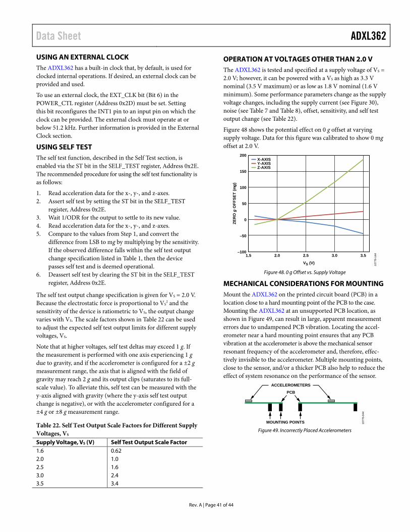
Data Sheet ADXL362
Rev. A | Page 41 of 44
USING AN EXTERNAL CLOCK The ADXL362 has a built-in clock that, by default, is used for clocked internal operations. If desired, an external clock can be provided and used.
To use an external clock, the EXT_CLK bit (Bit 6) in the POWER_CTL register (Address 0x2D) must be set. Setting this bit reconfigures the INT1 pin to an input pin on which the clock can be provided. The external clock must operate at or below 51.2 kHz. Further information is provided in the External Clock section.
USING SELF TEST The self test function, described in the Self Test section, is enabled via the ST bit in the SELF_TEST register, Address 0x2E. The recommended procedure for using the self test functionality is as follows:
1. Read acceleration data for the x-, y-, and z-axes. 2. Assert self test by setting the ST bit in the SELF_TEST
register, Address 0x2E. 3. Wait 1/ODR for the output to settle to its new value. 4. Read acceleration data for the x-, y-, and z-axes. 5. Compare to the values from Step 1, and convert the
difference from LSB to mg by multiplying by the sensitivity. If the observed difference falls within the self test output change specification listed in Table 1, then the device passes self test and is deemed operational.
6. Deassert self test by clearing the ST bit in the SELF_TEST register, Address 0x2E.
The self test output change specification is given for VS = 2.0 V. Because the electrostatic force is proportional to VS
2 and the sensitivity of the device is ratiometric to VS, the output change varies with VS. The scale factors shown in Table 22 can be used to adjust the expected self test output limits for different supply voltages, VS.
Note that at higher voltages, self test deltas may exceed 1 g. If the measurement is performed with one axis experiencing 1 g due to gravity, and if the accelerometer is configured for a ±2 g measurement range, the axis that is aligned with the field of gravity may reach 2 g and its output clips (saturates to its full-scale value). To alleviate this, self test can be measured with the y-axis aligned with gravity (where the y-axis self test output change is negative), or with the accelerometer configured for a ±4 g or ±8 g measurement range.
Table 22. Self Test Output Scale Factors for Different Supply Voltages, VS Supply Voltage, VS (V) Self Test Output Scale Factor 1.6 0.62 2.0 1.0 2.5 1.6 3.0 2.4 3.5 3.4
OPERATION AT VOLTAGES OTHER THAN 2.0 V The ADXL362 is tested and specified at a supply voltage of VS = 2.0 V; however, it can be powered with a VS as high as 3.3 V nominal (3.5 V maximum) or as low as 1.8 V nominal (1.6 V minimum). Some performance parameters change as the supply voltage changes, including the supply current (see Figure 30), noise (see Table 7 and Table 8), offset, sensitivity, and self test output change (see Table 22).
Figure 48 shows the potential effect on 0 g offset at varying supply voltage. Data for this figure was calibrated to show 0 mg offset at 2.0 V.
–100
–50
0
50
100
150
200
1.5 2.0 2.5 3.0 3.5
ZER
Og
OFF
SET
(mg)
X-AXISY-AXISZ-AXIS
VS (V)
1077
6-14
4
Figure 48. 0 g Offset vs. Supply Voltage
MECHANICAL CONSIDERATIONS FOR MOUNTING Mount the ADXL362 on the printed circuit board (PCB) in a location close to a hard mounting point of the PCB to the case. Mounting the ADXL362 at an unsupported PCB location, as shown in Figure 49, can result in large, apparent measurement errors due to undampened PCB vibration. Locating the accel-erometer near a hard mounting point ensures that any PCB vibration at the accelerometer is above the mechanical sensor resonant frequency of the accelerometer and, therefore, effec-tively invisible to the accelerometer. Multiple mounting points, close to the sensor, and/or a thicker PCB also help to reduce the effect of system resonance on the performance of the sensor.
MOUNTING POINTS
PCB
ACCELEROMETERS
1077
6-04
4
Figure 49. Incorrectly Placed Accelerometers
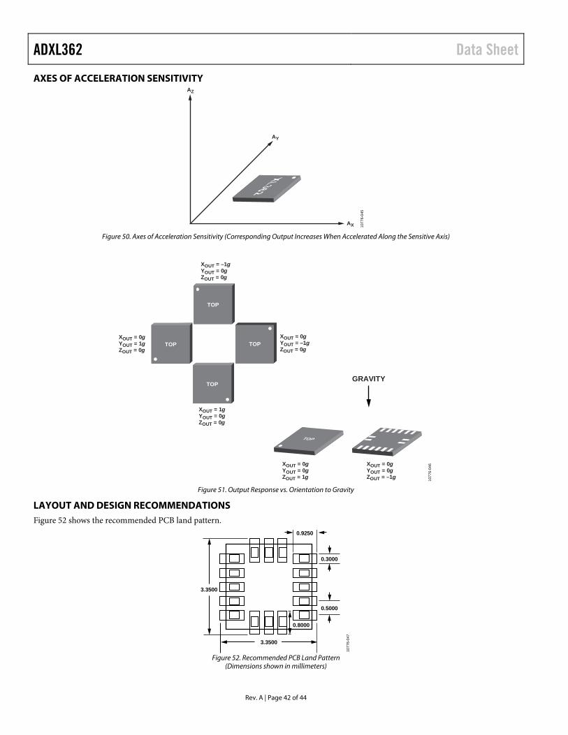
ADXL362 Data Sheet
Rev. A | Page 42 of 44
AXES OF ACCELERATION SENSITIVITY AZ
AY
AX 1077
6-04
5
Figure 50. Axes of Acceleration Sensitivity (Corresponding Output Increases When Accelerated Along the Sensitive Axis)
XOUT = –1gYOUT = 0gZOUT = 0g
GRAVITY
XOUT = 0gYOUT = 1gZOUT = 0g
XOUT = 0gYOUT = –1gZOUT = 0g
XOUT = 1gYOUT = 0gZOUT = 0g
XOUT = 0gYOUT = 0gZOUT = 1g
XOUT = 0gYOUT = 0gZOUT = –1g
TOP
TOP TOP
TOP
1077
6-04
6
Figure 51. Output Response vs. Orientation to Gravity
LAYOUT AND DESIGN RECOMMENDATIONS Figure 52 shows the recommended PCB land pattern.
0.8000
0.3000
0.5000
0.9250
3.3500
3.3500
1077
6-04
7
Figure 52. Recommended PCB Land Pattern
(Dimensions shown in millimeters)
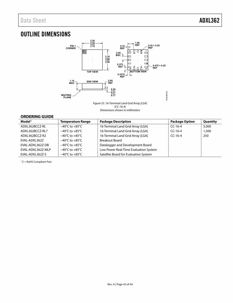
Data Sheet ADXL362
Rev. A | Page 43 of 44
OUTLINE DIMENSIONS
Figure 53. 16-Terminal Land Grid Array [LGA]
(CC-16-4) Dimensions shown in millimeters
ORDERING GUIDE Model1 Temperature Range Package Description Package Option Quantity ADXL362BCCZ-RL −40°C to +85°C 16-Terminal Land Grid Array [LGA] CC-16-4 5,000 ADXL362BCCZ-RL7 −40°C to +85°C 16-Terminal Land Grid Array [LGA] CC-16-4 1,500 ADXL362BCCZ-R2 −40°C to +85°C 16-Terminal Land Grid Array [LGA] CC-16-4 250 EVAL-ADXL362Z −40°C to +85°C Breakout Board EVAL-ADXL362Z-DB −40°C to +85°C Datalogger and Development Board EVAL-ADXL362Z-MLP −40°C to +85°C Low Power Real-Time Evaluation System EVAL-ADXL362Z-S −40°C to +85°C Satellite Board for Evaluation System 1 Z = RoHS Compliant Part.
10
-23-
2012
-A
TOP VIEW BOTTOM VIEW
END VIEW
SEATINGPLANE
3.303.253.15PIN 1
CORNER
0.250.210.17
0.3375REF
0.375REF
1.14MAX
0.85REF
0.10REF
1.00REF
0.475 × 0.25 REF
0.35 × 0.25 REF
1
689
131614
5
0.50BSC3.10
3.002.90

ADXL362 Data Sheet
Rev. A | Page 44 of 44
NOTES
©2012 Analog Devices, Inc. All rights reserved. Trademarks and registered trademarks are the property of their respective owners. D10776-0-9/12(A)