digital power detector for wcdma...
TRANSCRIPT
ISSN 0280-5316 ISRN LUTFD2/TFRT--5815--SE
Digital Power Detector for WCDMA Transmitter
Robert Carlzén Robert Nilsson
Department of Automatic Control Lund University
June 2008


Lund University Department of Automatic Control Box 118 SE-221 00 Lund Sweden
Document name MASTER THESIS Date of issue June 2008 Document Number ISRN LUTFD2/TFRT--5815--SE
Author(s) Robert Carlzén and Robert Nilsson
Supervisor Jonas Persson and Magnus Nilsson at Ericsson AB, Lund Bo Bernhardsson, Automatic Control Lund (Examiner)
Sponsoring organization
Title and subtitle Digital Power Detector for WCDMA Transmitter (Digital effektdetektor för WCDMA-sändare)
Abstract A 3G mobile phone must have the ability to control its output power with high precision. A power detector is used to measure the actual power outputted by the power amplifier to the antenna. With higher data rates the traditional implementations with peak detectors have become very difficult to use, which is why true RMS detectors are needed. In this thesis the digital part of a true RMS detector for W-CDMA has been designed. The analog parts of the power detector form a quadrature demodulator that transforms the radio signal down to DC where it is occupies a band from 0 to 2 MHz. The measured power amplifier output signal is sampled at 1 MHz which prohibits direct calculation of the RMS voltage in the detector. Instead the detector uses the wave form generator output as a reference to determine the amplification in the transmitter chain which can then be used to find the output power (wave form generator output has constant known power). This requires time alignment of the two signals which is done using a least mean square method of correlation. Using the reference up-sampled to 104 MHz allows very good accuracy despite the low sample rate of the power amplifier signal. To overcome distortion in the power amplifier an additional distortion reducing algorithm has been developed. An estimate of the output power can be delivered after 100 µs and has a standard deviation of its error of 0.05 dB. The error from changing modulation type is limited to a maximum 0.04 dB, well below the specified 0.1 dB. The solution is accurate and modulation independent.
Keywords
Classification system and/or index terms (if any)
Supplementary bibliographical information ISSN and key title 0280-5316
ISBN
Language English
Number of pages 87
Recipient’s notes
Security classification
http://www.control.lth.se/publications/


Acknowledgements
We would like to thank the following people:
• Jonas Persson and Magnus Nilsson for their ubiquitous support as supervisors.
• Bo Bernhardsson for taking an interest in our work and offering to help despite a busy schedule.
• Anders Thorsén, Tagi Farzone and Stefan Nilsson for sharing their insight in power amplifiers and power control.
• Fredrik Tillman for some quick answers on TXLpf.
• Martina Hansson for her excellent cooking.

1. Introduction 1
1.1 Background 1
1.1.1 Mobile telephony history 1
1.1.2 Problem description 2
1.1.3 Power control internal algorithm 4
1.1.4 External peak detector 5
1.1.5 External true RMS detector 7
1.1.6 Internal true RMS detector 7
1.2 The aim and outline of the thesis 8
2. Model 11
2.1 Quadrature modulation introduction 12
2.1.1 Error Vector Magnitude 15
2.2 Crucial properties and requirements 16
2.2.1 ADC sample‐rate and precision 16
2.2.2 Modulation dependency 17
2.2.3 Temperature dependency 19
2.2.4 Miscellaneous problems 19
2.3 Specification 20
2.4 Matlab model 20
2.4.1 Program structure 20
2.4.2 Phenomena included in the model 24
3. Solution alternatives 27
3.1 Direct RMS calculation of sampled data 27
3.2 Comparing with reference signal 28
3.3 Time alignment 30

3.3.1 Requirements 30
3.3.2 Different metrics of correlation 31
3.3.3 Coarse time alignment 34
3.3.4 Fine time alignment 35
3.3.5 Interpolation of the reference 35
3.3.6 Conclusion 37
3.4 Gain calculation 38
3.5 Reducing impact of distortion 40
3.5.1 Reduced sample collection 42
3.5.2 Extended sample collection 42
3.5.3 Distorting the reference 43
3.5.4 Conclusion 43
3.6 Increasing sample‐rate or slice length 43
3.7 DC compensation 45
3.8 Filtering 46
4. Impact of error sources 49
4.1 Impact of ADC quantization 49
4.2 Impact of ADC sub sampling 50
4.3 Impact of LO phase noise 50
4.4 Impact of AM/PM distortion 52
4.5 Impact of AM/AM distortion 52
4.6 Impact of time misalignment 54
4.7 Impact of DC 55
4.8 Impact of band select filter 57
4.9 Impact of I/Q phase shift 58
5. Proposed solution 59
5.1 Errors when everything is combined 60

5.1.1 Results of different files 61
5.1.2 Result from 40 ms data file 62
5.2 Complexity 63
6. Conclusion 65
6.1 The competition 65
6.2 Future work 65
7. References 67
Appendix 1 1
Appendix 2 4
Appendix 3 5
Appendix 4 6
Terminology
3GPP ‐ 3rd Generation Partnership Project
ADC ‐ Analog to Digital Converter
AM ‐ Amplitude Modulation
AM/AM Distortion – Nonlinear amplitude transfer function
AM/PM Distortion – Nonlinear phase transfer function
AMPS ‐ Advanced Mobile Phone System
ASIC ‐ Application Specific Integrated Circuits
BER ‐ Bit Error Rate
D‐AMPS ‐ Digital Advanced Mobile Phone System
dBm ‐ Power measurement unit. x[dBm] = 10∙log10(P[mW])
DC ‐ Direct Current
EDGE ‐ Enhanced Data rates for GSM Evolution
EVM – Error Vector Magnitude
FDMA ‐ Frequency Division Multiple Access
FFT ‐ Fast Fourier Transform
GenADC ‐ General Purpose Analog to Digital Converter
GPRS ‐ General Packet Radio Service
LMS – Least Mean Square
LO ‐ Local Oscillator
LUT ‐ Look Up Table
MS ‐ Mean Square or Multiple Sclerosis
NMT ‐ Nordic Mobile Telephone
QPSK ‐ Quadrature Phase Shift Key
PA ‐ Power Amplifier
PAR ‐ Peak to Average Ratio
PCB ‐ Printed Circuit Board
PIA ‐ Power control Internal Algorithm
RF ‐ Radio Frequency
RMS ‐ Root Mean Square
SIR ‐ Signal‐to‐Interference Ratio
SMS ‐ Short Message Service
TDMA ‐ Time Division Multiple Access
TPC ‐ Transmit Power Control
TX ‐ Transmitter
TXLpf ‐ Transmitter Low Pass Filter
TXVia ‐ Transmitter V‐to‐I Amplifier
UE ‐ User Equipment
UMTS ‐ Universal Mobile Telecommunications System
VGA ‐ Variable Gain Amplifier
WFG ‐ Wave Form Generator
W‐CDMA ‐ Wideband Code Division Multiple Access


1
1. Introduction
1.1 Background
1.1.1 Mobile telephony history
The idea of radio telephones and cellular radio networks stems from the first half of the 20th century. The word cellular refers to the way a large area can be given radio access by dividing it into hexagonal cells. Base stations located in the junction between three cells service mobile units through three directional antennas (see Figure 1.1). The base stations are part of a wired network and mobile units can have their traffic handed over from one base station to another automatically.
Figure 1.1: Principal layout of a cellular radio network with base stations in the junctions. Each base station can service three hexagonal cells.
After a slow start, with bulky installations in cars, the mobile telephony market has grown ever faster as the miniaturization of electronics made telephones smaller and more affordable. Commercial use in large scale began in the 1980s with analog systems such as the NMT (Nordic Mobile Telephone) system in Sweden and AMPS (Advanced Mobile Phone System) in the USA, both
2
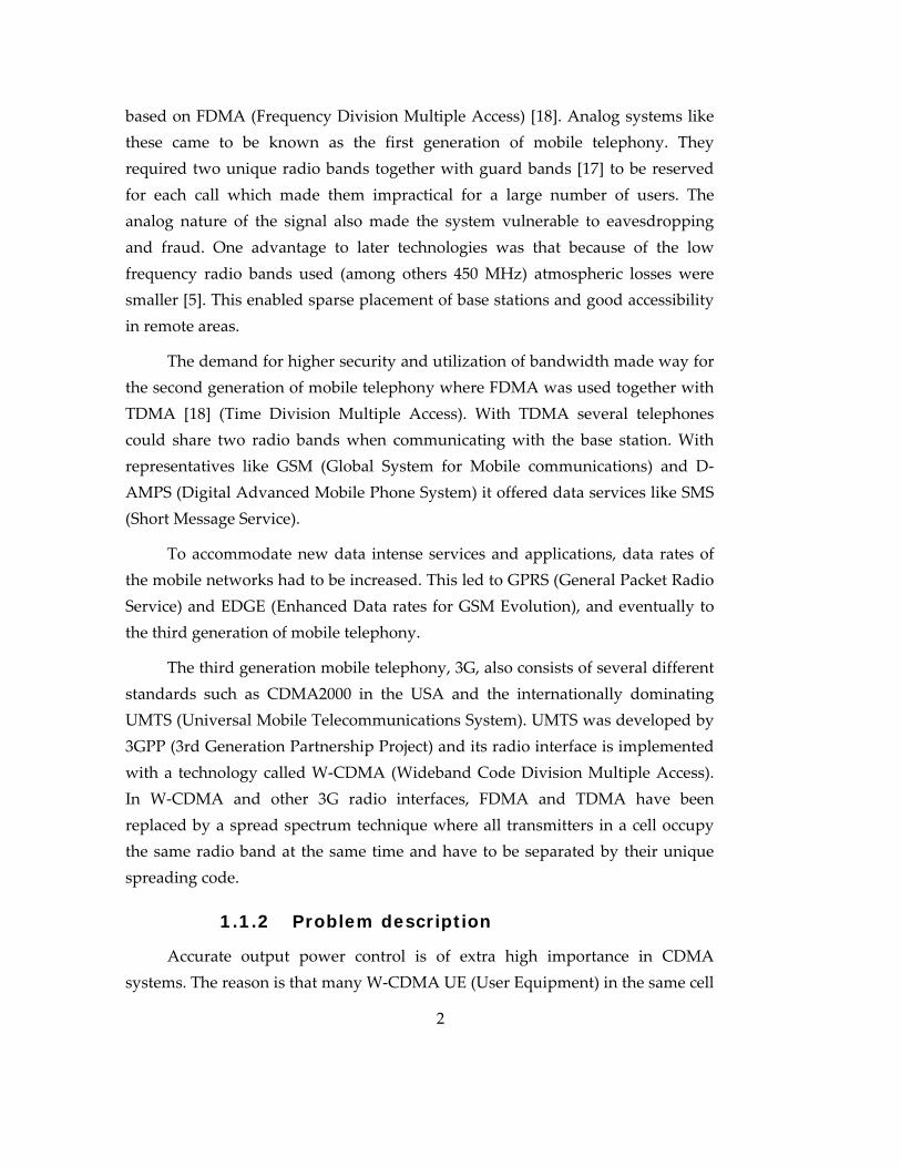
based on FDMA (Frequency Division Multiple Access) [18]. Analog systems like these came to be known as the first generation of mobile telephony. They required two unique radio bands together with guard bands [17] to be reserved for each call which made them impractical for a large number of users. The analog nature of the signal also made the system vulnerable to eavesdropping and fraud. One advantage to later technologies was that because of the low frequency radio bands used (among others 450 MHz) atmospheric losses were smaller [5]. This enabled sparse placement of base stations and good accessibility in remote areas.
The demand for higher security and utilization of bandwidth made way for the second generation of mobile telephony where FDMA was used together with TDMA [18] (Time Division Multiple Access). With TDMA several telephones could share two radio bands when communicating with the base station. With representatives like GSM (Global System for Mobile communications) and D‐AMPS (Digital Advanced Mobile Phone System) it offered data services like SMS (Short Message Service).
To accommodate new data intense services and applications, data rates of the mobile networks had to be increased. This led to GPRS (General Packet Radio Service) and EDGE (Enhanced Data rates for GSM Evolution), and eventually to the third generation of mobile telephony.
The third generation mobile telephony, 3G, also consists of several different standards such as CDMA2000 in the USA and the internationally dominating UMTS (Universal Mobile Telecommunications System). UMTS was developed by 3GPP (3rd Generation Partnership Project) and its radio interface is implemented with a technology called W‐CDMA (Wideband Code Division Multiple Access). In W‐CDMA and other 3G radio interfaces, FDMA and TDMA have been replaced by a spread spectrum technique where all transmitters in a cell occupy the same radio band at the same time and have to be separated by their unique spreading code.
1.1.2 Problem description
Accurate output power control is of extra high importance in CDMA systems. The reason is that many W‐CDMA UE (User Equipment) in the same cell
3
send their upload data simultaneously and in the same band which makes the radio signals mix at the base station antenna. In order to distinguish each signal from the others, every bit sent is multiplied with a unique spreading code vector. One bit is translated to a long sequence. Each spreading code is ideally orthogonal to all other spreading codes in use. The receiver can recover the original signal by using the same spreading code as the sender. Using truly orthogonal codes is however impractical since the codes are only orthogonal when completely in phase. Because the distance between the base station and different UEs varies, this is very unlikely. Instead, pseudo random sequences called PN‐codes are used. Their distribution is such that statistically they are nearly uncorrelated to each other independent of time delay.
Using the spreading code to distinguish one specific source from the received signal is possible but the signals sent by other UEs in the same cell can not be completely filtered out by the receiver. The power leaking between channels due to imperfect coding will act as interference and will be a significant contributor to the SIR (Signal‐to‐Interference Ratio). If output power was not controlled UEs transmitting in the vicinity of the base station would have their signals received at high power whilst signals received from more remote UEs would be faded and weak. The SIR for the different signals would then be very uneven and this would translate directly to the BER (bit error rate). This is commonly referred to a Near‐Far problem [2] and can be avoided by having the base station send TPC (Transmit Power Control) messages to the UEs. The 3GPP standard for W‐CDMA requires a UE to follow TPC ‐messages with specified accuracy [3].
The UE acts according to TPC commands by changing amplification settings for components in the TX (Transmit) chain. Unfortunately it is very hard to predict ‐ with wanted accuracy ‐ what affect a certain change of settings will have on the actual output power since the biasing of the PA will be changed to increase efficiency. The solution is to control the output power with negative feedback, which requires a signal which is proportional to the output power. For this sake a small portion of the signal intended for the antenna is diverted to a power detector. The output from the power detector can then be used in the power control internal algorithm.
4
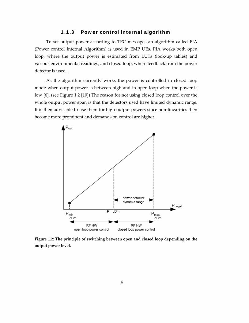
1.1.3 Power control internal algorithm
To set output power according to TPC messages an algorithm called PIA (Power control Internal Algorithm) is used in EMP UEs. PIA works both open loop, where the output power is estimated from LUTs (look‐up tables) and various environmental readings, and closed loop, where feedback from the power detector is used.
As the algorithm currently works the power is controlled in closed loop mode when output power is between high and in open loop when the power is low [6]. (see Figure 1.2 [10]) The reason for not using closed loop control over the whole output power span is that the detectors used have limited dynamic range. It is then advisable to use them for high output powers since non‐linearities then become more prominent and demands on control are higher.
Figure 1.2: The principle of switching between open and closed loop depending on the output power level.
5
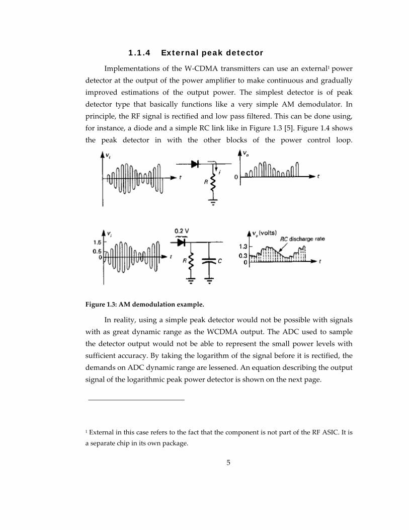
1.1.4 External peak detector
Implementations of the W‐CDMA transmitters can use an external1 power detector at the output of the power amplifier to make continuous and gradually improved estimations of the output power. The simplest detector is of peak detector type that basically functions like a very simple AM demodulator. In principle, the RF signal is rectified and low pass filtered. This can be done using, for instance, a diode and a simple RC link like in Figure 1.3 [5]. Figure 1.4 shows the peak detector in with the other blocks of the power control loop.
Figure 1.3: AM demodulation example.
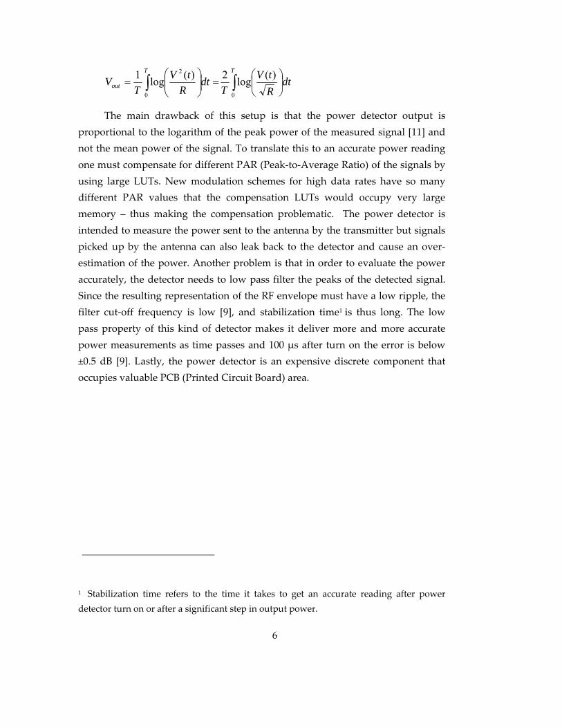
In reality, using a simple peak detector would not be possible with signals with as great dynamic range as the WCDMA output. The ADC used to sample the detector output would not be able to represent the small power levels with sufficient accuracy. By taking the logarithm of the signal before it is rectified, the demands on ADC dynamic range are lessened. An equation describing the output signal of the logarithmic peak power detector is shown on the next page.
1 External in this case refers to the fact that the component is not part of the RF ASIC. It is a separate chip in its own package.
6
∫∫ ⎟⎠
⎞⎜⎝
⎛=⎟⎟
⎠
⎞⎜⎜⎝
⎛=
TT
out dtRtV
Tdt
RtV
TV
00
2 )(log2)(log1
The main drawback of this setup is that the power detector output is proportional to the logarithm of the peak power of the measured signal [11] and not the mean power of the signal. To translate this to an accurate power reading one must compensate for different PAR (Peak‐to‐Average Ratio) of the signals by using large LUTs. New modulation schemes for high data rates have so many different PAR values that the compensation LUTs would occupy very large memory – thus making the compensation problematic. The power detector is intended to measure the power sent to the antenna by the transmitter but signals picked up by the antenna can also leak back to the detector and cause an over‐estimation of the power. Another problem is that in order to evaluate the power accurately, the detector needs to low pass filter the peaks of the detected signal. Since the resulting representation of the RF envelope must have a low ripple, the filter cut‐off frequency is low [9], and stabilization time1 is thus long. The low pass property of this kind of detector makes it deliver more and more accurate power measurements as time passes and 100 μs after turn on the error is below ±0.5 dB [9]. Lastly, the power detector is an expensive discrete component that occupies valuable PCB (Printed Circuit Board) area.
1 Stabilization time refers to the time it takes to get an accurate reading after power detector turn on or after a significant step in output power.

7
Figure 1.4: Principal block‐diagram of the transmitter and control circuitry when using a external peak detector.
1.1.5 External true RMS detector
To overcome the need for modulation compensation it would be desirable to use true RMS (Root Mean Square) detectors. A true RMS detector uses analog circuits that squares the RF signal and then filters it to get the power. Such detectors exist but not yet for this specific application. The equation below describes the output voltage.
⎟⎟⎠
⎞⎜⎜⎝
⎛= ∫
T
out dttVT
V0
2 )(1log
Even if a detector could be developed that meets all specifications, it would still retain some of the negative aspects of the old solution. It would occupy PCB area, be slow to converge, pricey and susceptible to interference from neighboring channels being picked up by the antenna. None of the current prototypes deliver accurate1 values faster than 250 μs after acquisition start.
1.1.6 Internal true RMS detector
Since a higher level of integration is one of the goals of each new platform generation it would be preferred that the power detector could be made a part of the RF ASIC (Radio Frequency Application Specific Integrated Circuit). The
1 Specified accuracy is a standard deviation of the error below 0.05 dB. See chapter 2.3.
PIA
PA
Peak detector A D
Coupler
Antenna
Bias
RF ASIC transmitter
8
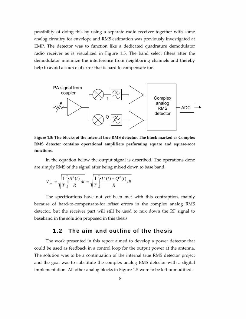
possibility of doing this by using a separate radio receiver together with some analog circuitry for envelope and RMS estimation was previously investigated at EMP. The detector was to function like a dedicated quadrature demodulator radio receiver as is visualized in Figure 1.5. The band select filters after the demodulator minimize the interference from neighboring channels and thereby help to avoid a source of error that is hard to compensate for.
Figure 1.5: The blocks of the internal true RMS detector. The block marked as Complex RMS detector contains operational amplifiers performing square and square‐root functions.
In the equation below the output signal is described. The operations done are simply RMS of the signal after being mixed down to base band.
∫∫+
==TT
out dtR
tQtIT
dtR
tST
V0
22
0
2 )()(1)(1
The specifications have not yet been met with this contraption, mainly because of hard‐to‐compensate‐for offset errors in the complex analog RMS detector, but the receiver part will still be used to mix down the RF signal to baseband in the solution proposed in this thesis.
1.2 The aim and outline of the thesis
The work presented in this report aimed to develop a power detector that could be used as feedback in a control loop for the output power at the antenna. The solution was to be a continuation of the internal true RMS detector project and the goal was to substitute the complex analog RMS detector with a digital implementation. All other analog blocks in Figure 1.5 were to be left unmodified.
ADC
I
Q
PA signal from coupler
Complex analog RMS
detector

9
With a new solution the drawbacks of the peak detector power control was to be avoided. The RF‐signal from the PA was to be fed back into the RF ASIC to eliminate the external power detector and save PCB area. The solution should be modulation independent which suggested the need for true RMS detection in one form or another.

11
2. Model
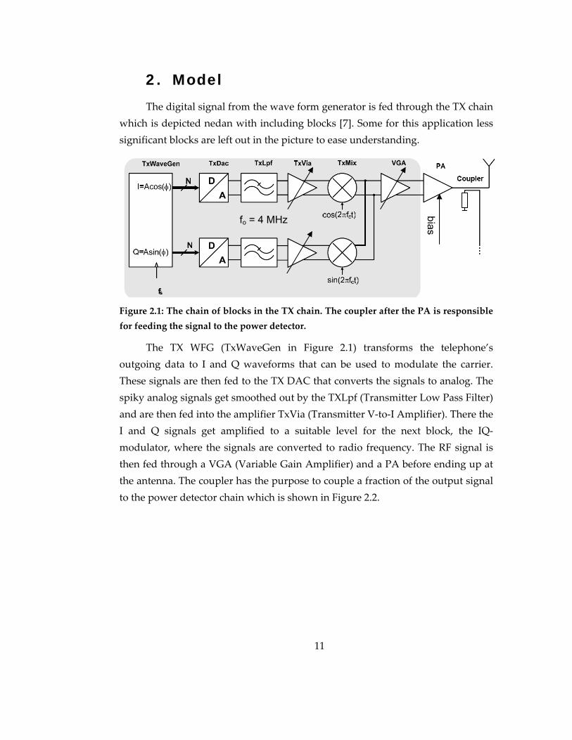
The digital signal from the wave form generator is fed through the TX chain which is depicted nedan with including blocks [7]. Some for this application less significant blocks are left out in the picture to ease understanding.
Figure 2.1: The chain of blocks in the TX chain. The coupler after the PA is responsible for feeding the signal to the power detector.
The TX WFG (TxWaveGen in Figure 2.1) transforms the telephone’s outgoing data to I and Q waveforms that can be used to modulate the carrier. These signals are then fed to the TX DAC that converts the signals to analog. The spiky analog signals get smoothed out by the TXLpf (Transmitter Low Pass Filter) and are then fed into the amplifier TxVia (Transmitter V‐to‐I Amplifier). There the I and Q signals get amplified to a suitable level for the next block, the IQ‐modulator, where the signals are converted to radio frequency. The RF signal is then fed through a VGA (Variable Gain Amplifier) and a PA before ending up at the antenna. The coupler has the purpose to couple a fraction of the output signal to the power detector chain which is shown in Figure 2.2.
fo = 4 MHz
bias
12
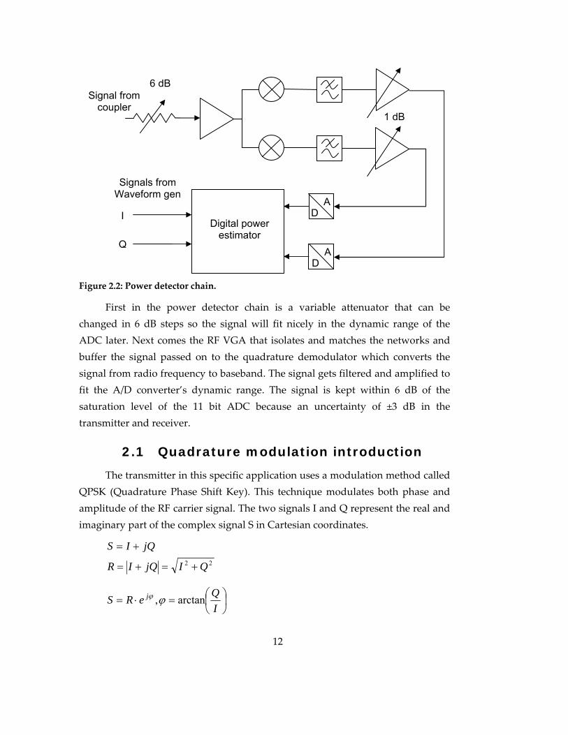
Figure 2.2: Power detector chain.
First in the power detector chain is a variable attenuator that can be changed in 6 dB steps so the signal will fit nicely in the dynamic range of the ADC later. Next comes the RF VGA that isolates and matches the networks and buffer the signal passed on to the quadrature demodulator which converts the signal from radio frequency to baseband. The signal gets filtered and amplified to fit the A/D converter’s dynamic range. The signal is kept within 6 dB of the saturation level of the 11 bit ADC because an uncertainty of ±3 dB in the transmitter and receiver.
2.1 Quadrature modulation introduction
The transmitter in this specific application uses a modulation method called QPSK (Quadrature Phase Shift Key). This technique modulates both phase and amplitude of the RF carrier signal. The two signals I and Q represent the real and imaginary part of the complex signal S in Cartesian coordinates.
22 QIjQIR
jQIS
+=+=
+=
⎟⎠⎞
⎜⎝⎛=⋅=
IQeRS j arctan,ϕϕ
Digital power estimator
Signal from coupler
Signals from Waveform gen
ADI
Q A
D
6 dB
1 dB
13
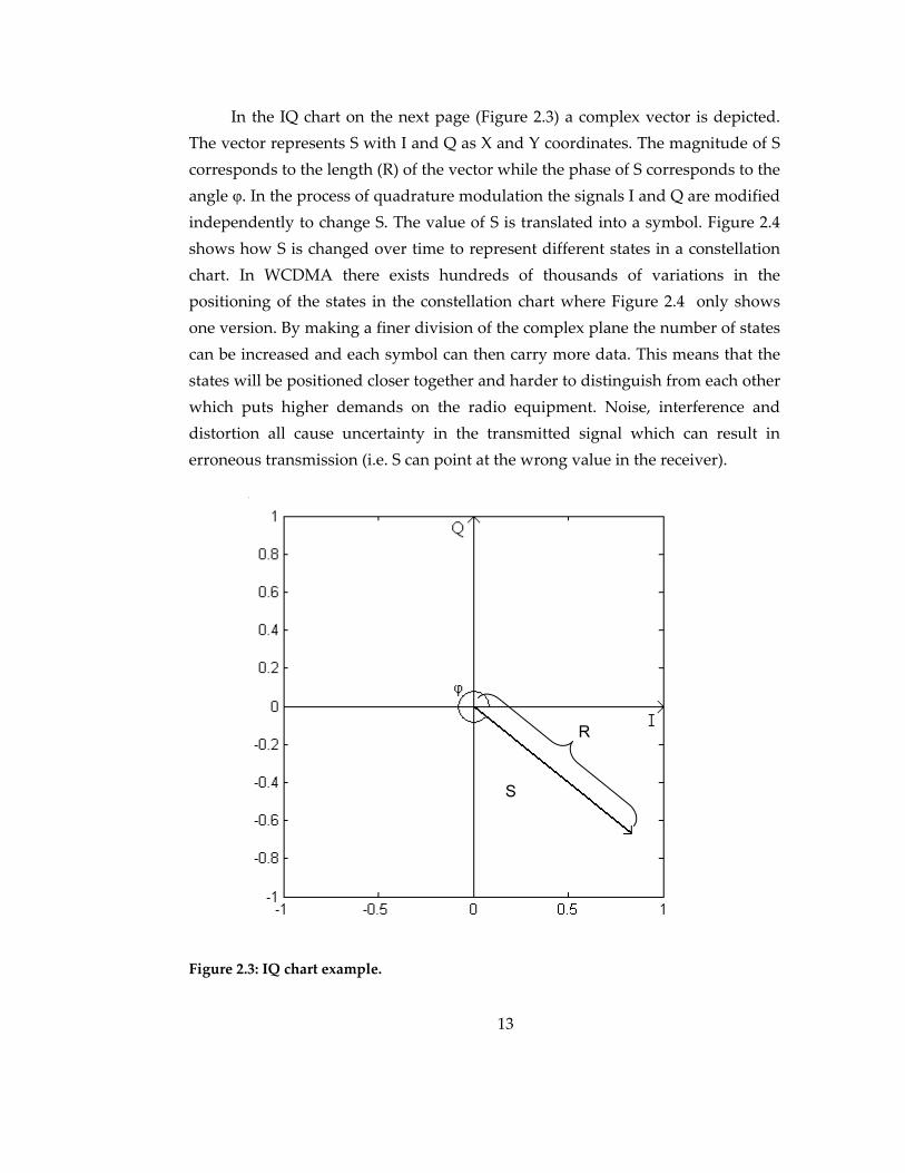
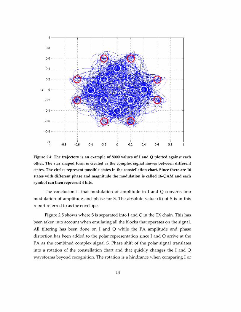
In the IQ chart on the next page (Figure 2.3) a complex vector is depicted. The vector represents S with I and Q as X and Y coordinates. The magnitude of S corresponds to the length (R) of the vector while the phase of S corresponds to the angle φ. In the process of quadrature modulation the signals I and Q are modified independently to change S. The value of S is translated into a symbol. Figure 2.4 shows how S is changed over time to represent different states in a constellation chart. In WCDMA there exists hundreds of thousands of variations in the positioning of the states in the constellation chart where Figure 2.4 only shows one version. By making a finer division of the complex plane the number of states can be increased and each symbol can then carry more data. This means that the states will be positioned closer together and harder to distinguish from each other which puts higher demands on the radio equipment. Noise, interference and distortion all cause uncertainty in the transmitted signal which can result in erroneous transmission (i.e. S can point at the wrong value in the receiver).
Figure 2.3: IQ chart example.
R
S
14
Figure 2.4: The trajectory is an example of 8000 values of I and Q plotted against each other. The star shaped form is created as the complex signal moves between different states. The circles represent possible states in the constellation chart. Since there are 16 states with different phase and magnitude the modulation is called 16‐QAM and each symbol can then represent 4 bits.
The conclusion is that modulation of amplitude in I and Q converts into modulation of amplitude and phase for S. The absolute value (R) of S is in this report referred to as the envelope.
Figure 2.5 shows where S is separated into I and Q in the TX chain. This has been taken into account when emulating all the blocks that operates on the signal. All filtering has been done on I and Q while the PA amplitude and phase distortion has been added to the polar representation since I and Q arrive at the PA as the combined complex signal S. Phase shift of the polar signal translates into a rotation of the constellation chart and that quickly changes the I and Q waveforms beyond recognition. The rotation is a hindrance when comparing I or

15
Q signals before and after TX processing with respect to amplitude. This forces the use of the envelope (amplitude of S) when doing this comparison.
S
Im{S}
Re{S}
cos(ωt)
-sin(ωt)
Split real & imag. parts
Pulse-shaping
Pulse-shaping
Figure 2.5: A reduced version of the TX chain showing the complex properties of the signal. [19]
2.1.1 Error Vector Magnitude
Error Vector Magnitude (EVM) shows how accurate the measured symbol is compared to the ideal one.
In Figure 2.6, v is the ideal symbol vector, w is the measured symbol vector and e = w – v is the resulting error vector i.e. the difference between the actual measured and ideal symbol vectors. |w| ‐ |v| is the magnitude error, θ is the phase error and 100∙|e|/|v| is the EVM (in %).
Figure 2.6: Error vector in IQ chart [22].
TXWaveGen (WFG)

16
The reason for expressing EVM as a percentage is to remove the dependency of system gain. In this application EVM is specified to 17.5%.
2.2 Crucial properties and requirements
The signal is passed through several blocks that will affect the signal’s properties in unwanted ways. Noise, distortion and time delay will be added through the chain and has to be investigated. It is crucial to have accurate data on the gain of the analog parts of the power detector since the uncertainty of this factor will translate directly to error in the absolute power estimation. Relative power estimations are only sensitive to changes that occur between two sequential measurements. Variation of temperature or supply voltage could cause some parameters to change but this occurs gradually over time and is thus negligible. RC‐calibration of the TXLpf could induce abrupt changes in output power but this function is only executed at data transfer start up.
2.2.1 ADC sample-rate and precision
The assumed GenADC (General Purpose Analog to Digital Converter) has a limited performance when it comes to sample‐rate and resolution. It can ideally deliver data with 11 bit precision in 1 MHz sample‐rate which is quite insufficient to correctly represent the I and Q signals since they have 2 MHz bandwidth. The fact that the sample‐rate of the signal is less than double the highest frequency content of the analog signal means that the Nyquist condition is not met [14]. When this is the case the signal will be referred to as sub‐sampled.
17
Although the ADC has an ideal precision of 11 bits the effective resolution is not expected to be nearly as high. This is due to averaging1 of ADC errors being disabled when operating at 1 MHz and a maximum back off of the signal from the receiver of ‐6 dB 2 . Offset errors, integral nonlinearity and differential nonlinearity in the GenADC give errors that amount to a maximum of 11.8 LSB s error. This results in a loss of about four bits. The maximum back‐off of the receiver will then put another bit out of play leaving only 6 bits to represent the voltage.
The goal of this investigation is to use a simple ADC design since it is efficient with respect to current consumption and chip area. An improved performance would require time for design, increasing production costs as well as decreasing the battery time of the product.
2.2.2 Modulation dependency
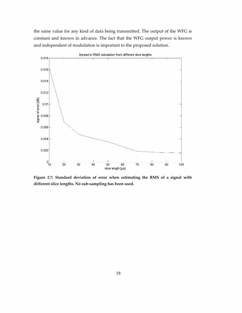
To avoid modulation dependency the RMS voltage of the signal has to be measured or correctly estimated as opposed to measuring the peak value of the output signal. The RMS voltage of the signal is not constant when looking at a limited segment which is what has to be done when detecting the power. Assuming that a stable RMS voltage is sought, the data acquisition time and sample‐rate must be such that variations are acceptable. Figure 2.7 reveals the RMS voltage variation when using different number of samples in the calculation. The example uses 52 MHz sample‐rate, i.e. the same as the WFG output. Using sub‐sampled data from the GenADC means even greater variations in calculated RMS voltage. Using an infinite acquisition time would result in a perfect RMS voltage calculation. Doing this for the unmodified WFG output would result in
1 Precision can be upheld despite offset errors in the ADC if a number of sequential measurements are averaged. This lowers the sample‐rate of the output accordingly.
2 The receiver has VGAs just prior to the ADC inputs. These amplifiers see to it that the peaks of the signals to digitize are never smaller than half of the voltage required to saturate the ADCs. The nominal back off is ‐3 dB with since there is an uncertainty of 3 dB in the TX gain settings.
18
the same value for any kind of data being transmitted. The output of the WFG is constant and known in advance. The fact that the WFG output power is known and independent of modulation is important to the proposed solution.
Figure 2.7: Standard deviation of error when estimating the RMS of a signal with different slice lengths. No sub‐sampling has been used.

19
2.2.3 Temperature dependency
All blocks will be affected in some way by temperature changes. To avoid these problems the temperature properties of every block have to be investigated. The results can then be used to predict and compensate for deviations due to temperature changes. The compensation of the analog errors has to be done in the digital parts by using LUTs. On the other hand, this was not a problem to solve in this thesis and will therefore not be discussed any further.
2.2.4 Miscellaneous problems
In the analog blocks of the power estimator chain there are parameters like nonlinearities, gain offsets, battery voltage ripple and process variations that will affect the signal reaching the ADC. These have to be compensated for in the same way as the temperature errors and will similarly be left for future work.
20
2.3 Specification
The most interesting figure in the specification is the one that regulates the maximum error caused by variations in modulation (e.g. variations in PAR). This has been labeled Error from modulation. Other critical requirements are the standard deviation of the power estimation error and the measuring time. The current consumption requirements have been ignored since the analog receiver block currents will dominate over the digital part presented in this thesis. The specification is presented in Table 1.
Table 1: Specification for power detector.
Error from modulation ± 0.1 dB
Standard deviation of error 0.05 dB
Measuring time 100 µs
2.4 Matlab model
As a basis for the investigations into modulation independent power detection, a set of data files with differently modulated WFG output data has been used. These six pairs of files (pairs of I and Q data) represent different cases with different PAR which makes them valid for testing modulation independency. For all tests presented in this report the 5760wc files have been used if nothing else is explicitly written.
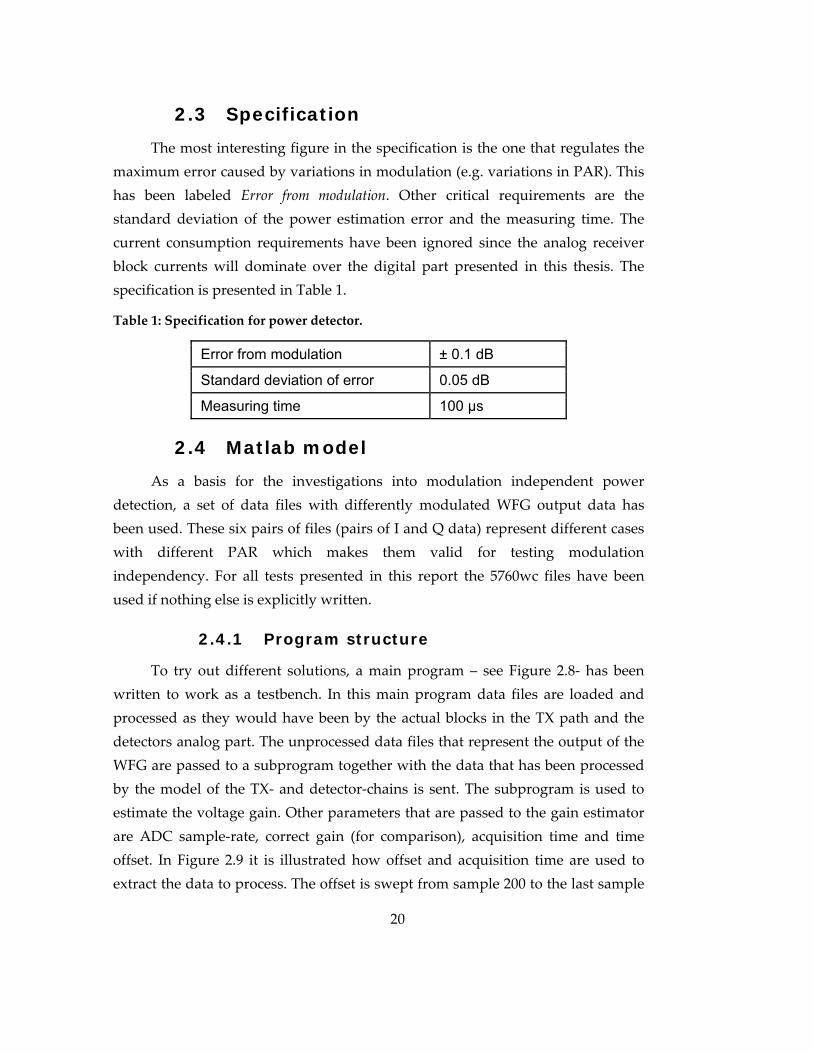
2.4.1 Program structure
To try out different solutions, a main program – see Figure 2.8‐ has been written to work as a testbench. In this main program data files are loaded and processed as they would have been by the actual blocks in the TX path and the detectors analog part. The unprocessed data files that represent the output of the WFG are passed to a subprogram together with the data that has been processed by the model of the TX‐ and detector‐chains is sent. The subprogram is used to estimate the voltage gain. Other parameters that are passed to the gain estimator are ADC sample‐rate, correct gain (for comparison), acquisition time and time offset. In Figure 2.9 it is illustrated how offset and acquisition time are used to extract the data to process. The offset is swept from sample 200 to the last sample
21
of the data file. This is to make sure that every case is covered in the simulation except a small start up time of the WFG. The length of the slice is the same as the acquisition time in μs if a 1 MHz ADC is used.
Figure 2.8: Program structure of the testbench.
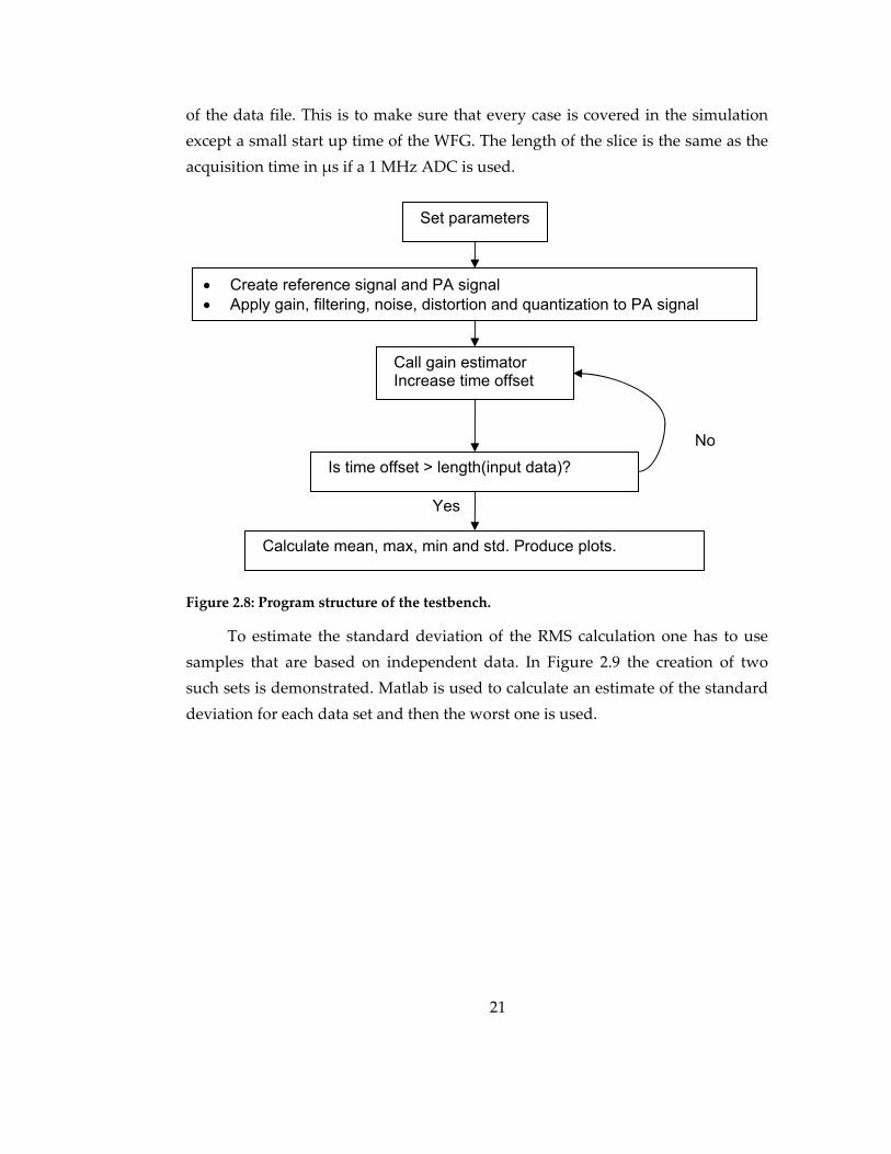
To estimate the standard deviation of the RMS calculation one has to use samples that are based on independent data. In Figure 2.9 the creation of two such sets is demonstrated. Matlab is used to calculate an estimate of the standard deviation for each data set and then the worst one is used.
Set parameters
Call gain estimator Increase time offset
Is time offset > length(input data)?
Calculate mean, max, min and std. Produce plots.
No
Yes
• Create reference signal and PA signal • Apply gain, filtering, noise, distortion and quantization to PA signal
22
Figure 2.9: The two upper slices are independent of each other. When extracting a slice and taking a step of the slice length before cutting the next one out, one will get two independent RMS calculations. Iterating this for the whole data file will give a number of different powers which can be used for standard deviation estimation. To cover all cases the time offset is increased by 1 and a new set of slices is extracted and used for calculation. The data in the example is a Q signal at full resolution.
Slice length
Time offset
23
It is not enough in it self to make an estimate of the standard deviation of the error. It is important to make sure that the limit set by the specification is not exceeded with a known probability. It will now be shown how to specify an upper limit for s (estimated σ) so that the specified maximum σ of 0.05 dB is not exceeded with 99% certainty. Other confidence levels could be considered but since no particular level was specified 0.99 was chosen based on its common use.
( )( )
5101.0
11,0
12
2
2
==
⎥⎦
⎤⎢⎣
⎡
−⋅−
=−
n
nsnI
αχ α
σ
k = 0.05 dB [12]
s = estimated σ
n corresponds to the number of uncorrelated gain calculations that are used to estimate σ.
( ) 7.295095.02 =χ [13]
( )( )
( )1
11
1 12
2
12
2
−−
≤⇔≤−⋅− −
− nnksk
nsn α
α
χχ
( )( )
0385.0001485.0
001485.050
7.2905.005.01
1 22
12
2
≈=
≈⋅
=⇔=−⋅−
−
s
sn
snαχ
The result implies that the estimated standard deviation should stay below 0.0385 to make sure that with 99% certainty the standard deviation will not exceed the 0.05 limit when doing 51 calculations.
To meet specification with a confidence of 99% some tests will be run on longer sequences and thus have a larger number of samples for estimation of the standard deviation. Limits for these tests must also be calculated.
n=101 => s=0.0419 ca 10 ms of data
n=201 => s=0.0442 ca 20 ms of data
n=401 => s=0.0459 ca 40 ms of data
24
2.4.2 Phenomena included in the model
To try out ideas and to put algorithms to the test some troublesome aspects of the signal’s path have been modeled in the testbench. The first block that is modeled in the testbench is the TXLpf. The analog low‐pass filter has a nominal cut‐off frequency of 4 MHz. The actual cut‐off frequency can deviate from this value. To model this, the filter was emulated as a third order FIR‐filter with a cut‐off frequency of 3.8 MHz. This affects the frequency contents of the signal and also introduces some delay.
The next blocks to be included are the transmitter mixers. These are used to up‐convert the baseband signal to RF and does this by multiplying the signal with the output of a LO (Local Oscillator). The LO and the dividers that it is processed by1, have a phase uncertainty which is a Gaussian noise. This has been modeled as having a standard deviation of 1.5° and 150 kHz bandwidth. A noise vector with these properties has then been added to the phase of the signal in its polar representation (i.e. arg(S)) to emulate the noise injected by the LO. Phase noise does translate to noise in I and Q but the noise is absolutely correlated and when reverting back to polar representation the envelope is unchanged. Because of the channel select filters the effect could be loss of power.
1 Leakage of the LO to other parts of the radio must be avoided. By operating the actual oscillator at double the carrier‐frequency it can not do as much harm. The LO signal is then divided to the carrier‐frequency close to the mixer.
25
The PA is also included in the model. It has significant effect on the signal in polar form (S) with AM/AM distortion1 and AM/PM distortion2. The data used can be found in Appendix 2. When using the PA data it is assumed that the input signal level does not exceed 0.3 V3, which then includes the most linear region and the gain‐expansion region.
The receiver mixers have similar effect on the signal properties as the transmitter dittos. It is thus modeled with the addition of the same noise vector to the phase of S. The total phase noise therefore gets the RMS value 3° [23]. Another effect that the receiver mixers could be responsible for is the addition of a DC‐offset to the output signals. This is investigated thoroughly in chapter 4.7 but not included in the final test bench. The error is better emulated by running the DC‐removal algorithm (3.7) since the resulting error then is independent on applied DC. Because the signal S has been somewhat delayed since its up‐conversion (due to its path through PA, coupler etc) its phase will be different when the RF signal is down‐converted again. This will translate to a static phase shift of S which means a rotation in the IQ chart. The effect of this is marginal and has thus been excluded from the testbench.
Among the blocks that are included in the model are also the 10 MHz (nominal) low‐pass filters of the receiver. These are modeled with first order FIR‐filters with a cut‐off frequency of 7 MHz since there is a possibility of a spread of ±30% due to temperature and process variations (RC‐calibration could be implemented to reduce spread). This affects the frequency contents of the signal and also introduces some delay.
1 AM/AM distortion means nonlinear amplitude transfer function.
2 AM/PM distortion means that the output phase is dependent on the input voltage.
3 Amplitude of the envelope signal is assumed to be 1 V to start with. This is slightly incorrect since there are peaks that exceed this value. These peaks are very rare though.
Amplitude of the envelope should be 2 since amplitude of I and Q is 1 but the modulation is such that this state is avoided.
26
Noise from individual blocks have not been included in the model with the exception for the LO. The noise from transistors and resistive elements is commonly included in the EVM specification. In this simulation the EVM has instead been broken down into major contributors like phase noise, AM/AM and AM/PM distortion. The noise constitutes only 0.5% of the total EVM and has thus been excluded [1].
Lastly, the GenADC is introduced in the testbench. Besides limiting the number of samples that can be used for the algorithm, it also introduces quantization noise. This noise is modeled by limiting the resolution of the signal to 26 levels.
One effect that has been left out is mismatch in I and Q filters that might cause amplitude and phase asymmetry between I and Q. Any effect that the coupler may have, as well as impact from the variable attenuator that follows, has also been ignored. The resolution of the transmitter DAC generates a noise that is believed negligible and has therefore been left out. The noise from amplifiers and their resistive components are neglected as well.
27
3. Solution alternatives
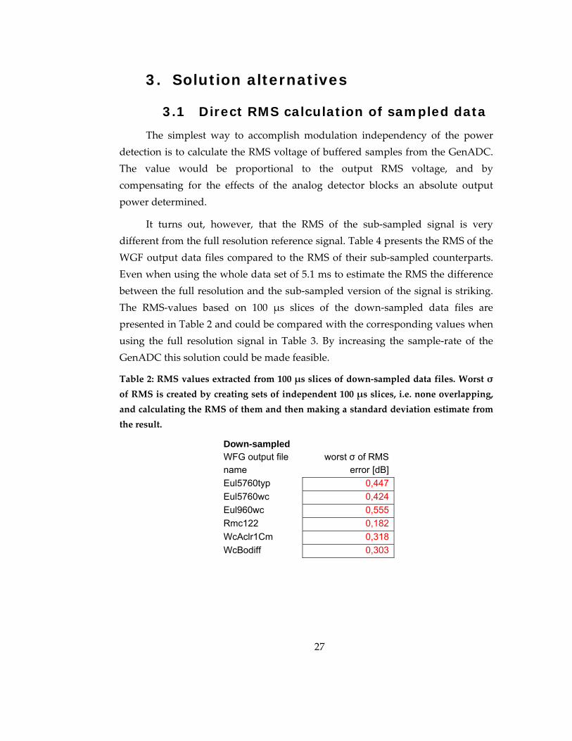
3.1 Direct RMS calculation of sampled data
The simplest way to accomplish modulation independency of the power detection is to calculate the RMS voltage of buffered samples from the GenADC. The value would be proportional to the output RMS voltage, and by compensating for the effects of the analog detector blocks an absolute output power determined.
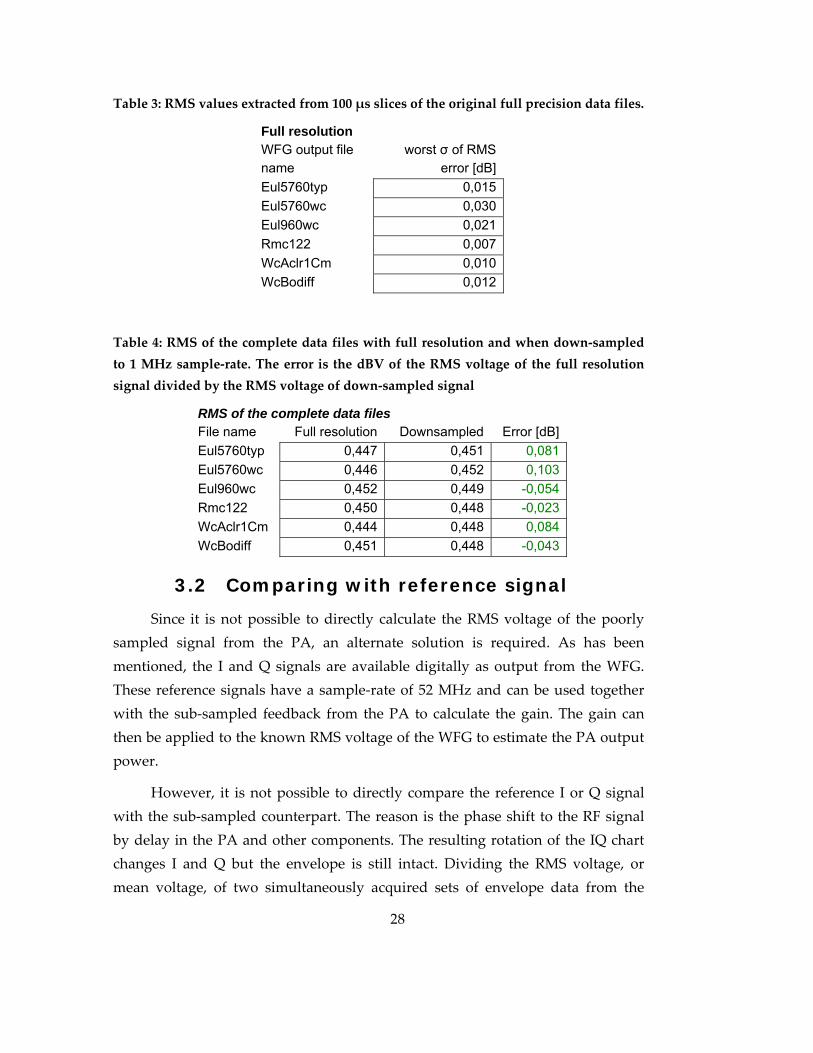
It turns out, however, that the RMS of the sub‐sampled signal is very different from the full resolution reference signal. Table 4 presents the RMS of the WGF output data files compared to the RMS of their sub‐sampled counterparts. Even when using the whole data set of 5.1 ms to estimate the RMS the difference between the full resolution and the sub‐sampled version of the signal is striking. The RMS‐values based on 100 μs slices of the down‐sampled data files are presented in Table 2 and could be compared with the corresponding values when using the full resolution signal in Table 3. By increasing the sample‐rate of the GenADC this solution could be made feasible.
Table 2: RMS values extracted from 100 μs slices of down‐sampled data files. Worst σ of RMS is created by creating sets of independent 100 μs slices, i.e. none overlapping, and calculating the RMS of them and then making a standard deviation estimate from the result.
Down-sampled WFG output file name
worst σ of RMS error [dB]
Eul5760typ 0,447Eul5760wc 0,424Eul960wc 0,555Rmc122 0,182WcAclr1Cm 0,318WcBodiff 0,303
28
Table 3: RMS values extracted from 100 μs slices of the original full precision data files.
Full resolution WFG output file name
worst σ of RMS error [dB]
Eul5760typ 0,015Eul5760wc 0,030Eul960wc 0,021Rmc122 0,007WcAclr1Cm 0,010WcBodiff 0,012
Table 4: RMS of the complete data files with full resolution and when down‐sampled to 1 MHz sample‐rate. The error is the dBV of the RMS voltage of the full resolution signal divided by the RMS voltage of down‐sampled signal
RMS of the complete data files File name Full resolution Downsampled Error [dB]Eul5760typ 0,447 0,451 0,081Eul5760wc 0,446 0,452 0,103Eul960wc 0,452 0,449 -0,054Rmc122 0,450 0,448 -0,023WcAclr1Cm 0,444 0,448 0,084WcBodiff 0,451 0,448 -0,043
3.2 Comparing with reference signal
Since it is not possible to directly calculate the RMS voltage of the poorly sampled signal from the PA, an alternate solution is required. As has been mentioned, the I and Q signals are available digitally as output from the WFG. These reference signals have a sample‐rate of 52 MHz and can be used together with the sub‐sampled feedback from the PA to calculate the gain. The gain can then be applied to the known RMS voltage of the WFG to estimate the PA output power.
However, it is not possible to directly compare the reference I or Q signal with the sub‐sampled counterpart. The reason is the phase shift to the RF signal by delay in the PA and other components. The resulting rotation of the IQ chart changes I and Q but the envelope is still intact. Dividing the RMS voltage, or mean voltage, of two simultaneously acquired sets of envelope data from the
29
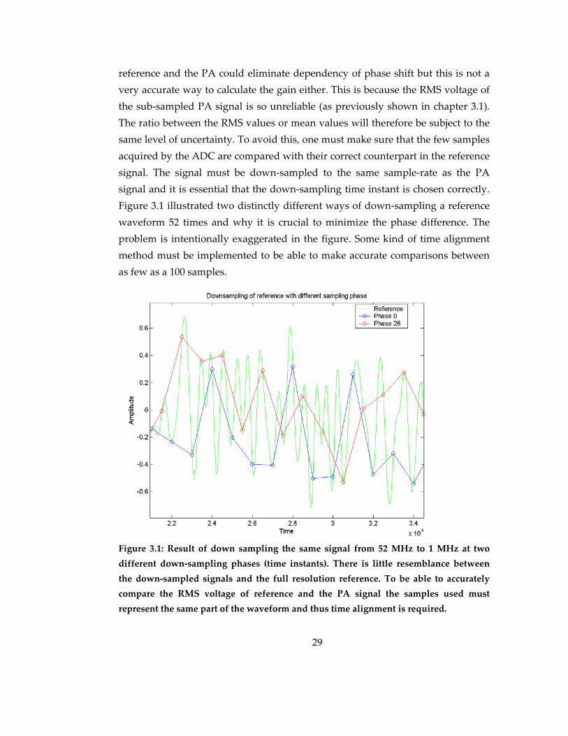
reference and the PA could eliminate dependency of phase shift but this is not a very accurate way to calculate the gain either. This is because the RMS voltage of the sub‐sampled PA signal is so unreliable (as previously shown in chapter 3.1). The ratio between the RMS values or mean values will therefore be subject to the same level of uncertainty. To avoid this, one must make sure that the few samples acquired by the ADC are compared with their correct counterpart in the reference signal. The signal must be down‐sampled to the same sample‐rate as the PA signal and it is essential that the down‐sampling time instant is chosen correctly. Figure 3.1 illustrated two distinctly different ways of down‐sampling a reference waveform 52 times and why it is crucial to minimize the phase difference. The problem is intentionally exaggerated in the figure. Some kind of time alignment method must be implemented to be able to make accurate comparisons between as few as a 100 samples.
Figure 3.1: Result of down sampling the same signal from 52 MHz to 1 MHz at two different down‐sampling phases (time instants). There is little resemblance between the down‐sampled signals and the full resolution reference. To be able to accurately compare the RMS voltage of reference and the PA signal the samples used must represent the same part of the waveform and thus time alignment is required.
30
3.3 Time alignment
If the measured signal from the PA is to be compared with the down‐sampled reference signal, time alignment is required before the down‐sampling occurs as has been described in the previous chapter. Time alignment is required because of the delay introduced by various components in the signal path from WFG to the PA and back through the dedicated receiver of the power detector. Blocks that introduce delay are the TXLpf, the PA and its RF filters, the band select filter of the receiver and the ADC. The contributions from the RF parts are neglected due to the high frequency. Filters in this frequency range have little group delay. The ADC has a fix conversion time of 1 μs making it the single largest cause of delay. The low pass filters also add significant delay. TXLpf has approximately 100 ns group‐delay and the band select filter group‐delay is approximately 16 ns. The time alignment algorithm should be made to investigate a span of different lags determined by the total delay of the loop and the extremes of its variance. An estimate range could be derived from a fixed delay of the ADC, small variation of the TXLpf since it is RC‐calibrated and +‐30% spread of the band select filter. The parts can then be summed up to get the total spread and nominal delay.
3.3.1 Requirements
When evaluating time alignment algorithms, the maximum residual time mismatch is used. It is assumed that the alignment has been successful but that it has left a delay between the signals which is as long as the resolution of the algorithm allows. This amounts to ½ a sample period of the one of the signals that has the highest sample rate.
How often the time alignment algorithm has to run depends on how quickly the delay of the TX chain varies with temperature and supply voltage. It is reasonable to focus on the changes of the cut‐off frequency of the TXLpf since this is the single largest contributor to the overall delay. The active components in the filter, i.e. the transistors, vary with supply voltage and temperature but the function of the filter is almost unchanged as long as the loop gain of the amplifier is high enough. The most important parameter then becomes the impact of temperature on the passive component values. Filter group delay has been
31
simulated and the temperature swept from ‐30°C to 100°C and the total change was about 2 ns [21] (2%). Assuming linear relation between temperature and group delay the group delay changes 13.3 ps/°C and knowing that the temperature gradient is maximally 2°C/s [9] this can be translated to 26.6 ps/s group delay.
3.3.2 Different metrics of correlation
All methods of aligning signals require some metric of how well correlated the compared vectors are. The standard and (in most aspects) best way is to use cross correlation which can be done both in time and frequency domain. The cross‐correlation formula according to [14] is
[ ] [ ] [ ]∑∞
−∞=
−=n
xy lnynxlr
where l is the number of lags. For a finite signal the sum will be limited to –N to N where N is the number of elements in the signal vector.
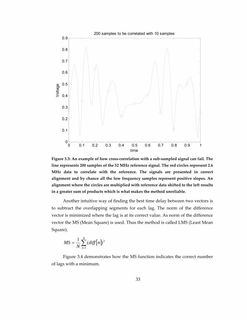
The equation above is basically an element‐wise multiplication of the overlapping parts of two vectors when they are slid over each other. A large product indicates good correlation for that delay which is shown in the example in Figure 3.2. This method enables finding the correct lag even under very noisy conditions, with distortion DC‐offset and gain. The problem with this method arises when using it with a sub‐sampled signal such as the one in this implementation. The goal was to use less than 100 samples to find the correlation with the reference signal. If these samples are not equally distributed between positive and negative slopes of the signal, an incorrect lag could slide a large number of samples to a position where they give a significantly larger contribution to the sum of products than the samples that are on the other slope. In Figure 3.3 this is demonstrated.
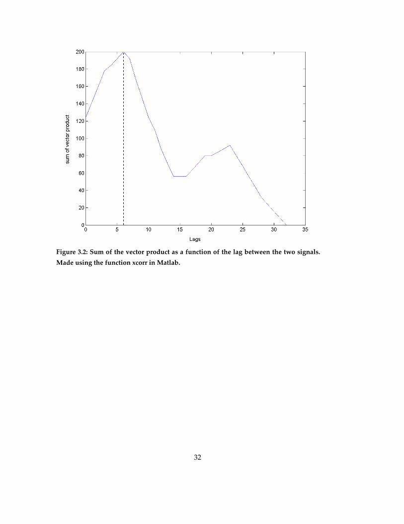
32
Figure 3.2: Sum of the vector product as a function of the lag between the two signals. Made using the function xcorr in Matlab.
33
0 0.1 0.2 0.3 0.4 0.5 0.6 0.7 0.8 0.9 1
0
0.1
0.2
0.3
0.4
0.5
0.6
0.7
0.8
0.9
time
Vol
tage
200 samples to be correlated with 10 samples
Figure 3.3: An example of how cross‐correlation with a sub‐sampled signal can fail. The line represents 200 samples of the 52 MHz reference signal. The red circles represent 2.6 MHz data to correlate with the reference. The signals are presented in correct alignment and by chance all the low frequency samples represent positive slopes. An alignment where the circles are multiplied with reference data shifted to the left results in a greater sum of products which is what makes the method unreliable.
Another intuitive way of finding the best time delay between two vectors is to subtract the overlapping segments for each lag. The norm of the difference vector is minimized where the lag is at its correct value. As norm of the difference vector the MS (Mean Square) is used. Thus the method is called LMS (Least Mean Square).
[ ]∑=
=N
nndiff
NMS
1
2)(1
Figure 3.4 demonstrates how the MS function indicates the correct number of lags with a minimum.

34
Figure 3.4: Correlation versus lags when using MS function. The minimum of the curve shows the correct estimated delay.
It is clear that the LMS method is superior to cross‐correlation. The LMS method is chosen.
3.3.3 Coarse time alignment
As determining the gain requires the two compared signals to be aligned in time, an algorithm to find the delay has to be devised. A fast but fairly inaccurate way to do this alignment would be to down sample the reference signal to the same sample‐rate as the signal after the GenADC and then use some kind of correlation metric for different delays. In Figure 7.5 in Appendix 4, the process of finding the delay which gives the best match is illustrated. The accuracy of this time alignment is limited by the sample‐rate of the GenADC. Assuming 1 MHz sample‐rate of the GenADC the span of the expected delay would be so close to 1 μs delay that this would be the most correct choice in every case thus making time alignment with this kind of precision redundant.
35
3.3.4 Fine time alignment
Instead of making one specific sub‐sampled version of the reference signal to use for time alignment, a number of possible versions can be used. The higher the sample‐rate of the reference is, the more combinations of down‐sampled reference and PA signal can be tested for correlation. By doing this, the maximum remaining time delay after successful alignment is half of the time between two samples in the reference. Figure 7.6 in Appendix 4 shows an example of performing fine time alignment with cross correlation method.
3.3.5 Interpolation of the reference
The reference signal sample‐rate is 52 MHz. If the specification of relative error is to be met, without modifying existing analog parts, one possibility is to increase the sample‐rate of the reference signal by interpolation. The remaining time error after alignment can then be reduced to any fraction of 1/52 μs at a cost of increased number of calculations (caused by more elements to align and the interpolation itself) and the additional error in the reference signal due to interpolation.
The spread in delay in the TX‐chain will be quite small which means only a few feasible delays have to be tested and compared. Since so few options are required the matter of interpolating the signal is limited to interpolating the parts of the signal that are actually to be used.
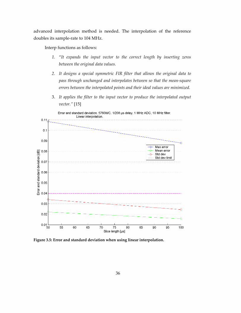
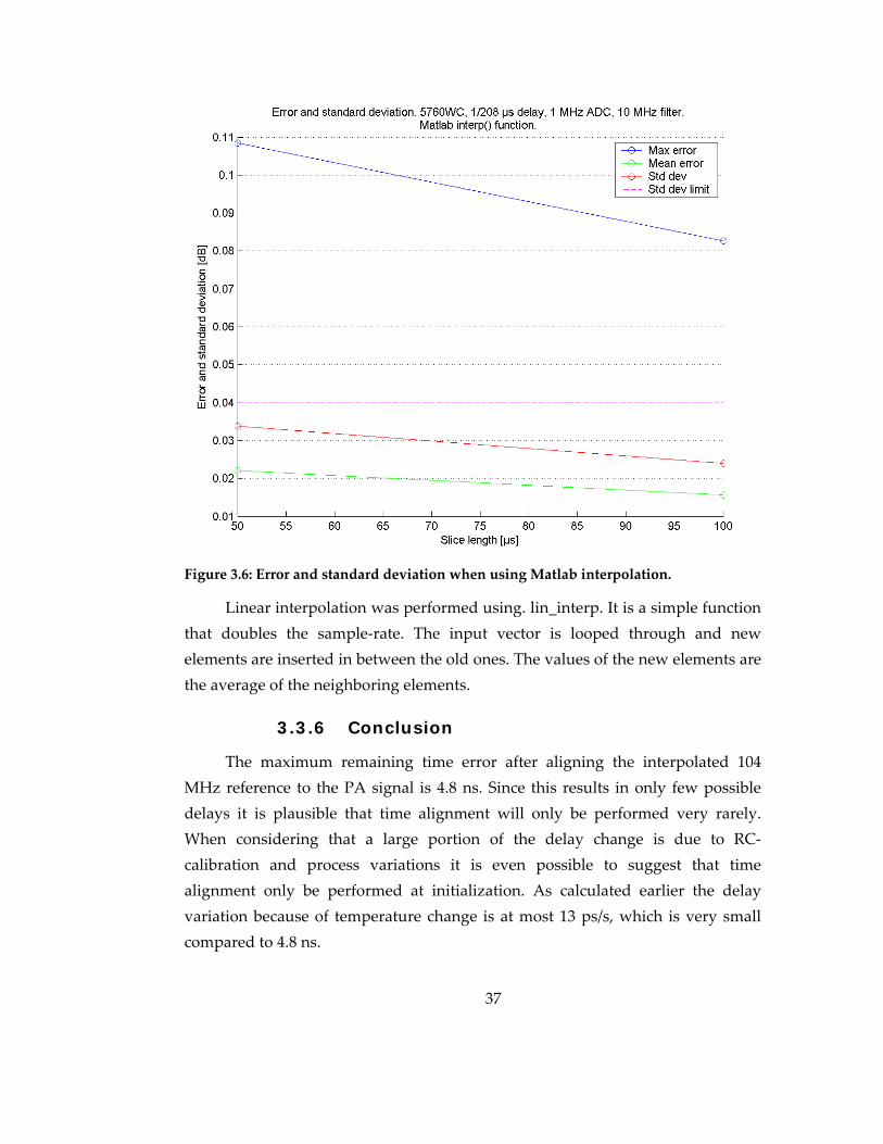
Interpolation methods
In Figure 3.5 and Figure 3.6, a comparison between two different interpolation methods, linear interpolation and Matlab interp()‐function, has been done. The test has performed with 50 μs and 100 μs slice lengths and the standard deviation and errors have been calculated. No error sources except for the small time delay were introduced. The result shows that for a longer slice length the Matlab interp() function generates better results for the max error. The standard deviation seems insensitive to interpolation method changes which can be explained by the already nearly perfect representation of the signal. Since the I and Q signals have such low frequency content in comparison with the sample‐rate of 52 MHz, the signals vary almost linearly between samples and no
36
advanced interpolation method is needed. The interpolation of the reference doubles its sample‐rate to 104 MHz.
Interp functions as follows:
1. “It expands the input vector to the correct length by inserting zeros between the original data values.
2. It designs a special symmetric FIR filter that allows the original data to pass through unchanged and interpolates between so that the mean‐square errors between the interpolated points and their ideal values are minimized.
3. It applies the filter to the input vector to produce the interpolated output vector.” [15]
Figure 3.5: Error and standard deviation when using linear interpolation.
37
Figure 3.6: Error and standard deviation when using Matlab interpolation.
Linear interpolation was performed using. lin_interp. It is a simple function that doubles the sample‐rate. The input vector is looped through and new elements are inserted in between the old ones. The values of the new elements are the average of the neighboring elements.
3.3.6 Conclusion
The maximum remaining time error after aligning the interpolated 104 MHz reference to the PA signal is 4.8 ns. Since this results in only few possible delays it is plausible that time alignment will only be performed very rarely. When considering that a large portion of the delay change is due to RC‐calibration and process variations it is even possible to suggest that time alignment only be performed at initialization. As calculated earlier the delay variation because of temperature change is at most 13 ps/s, which is very small compared to 4.8 ns.
38
3.4 Gain calculation
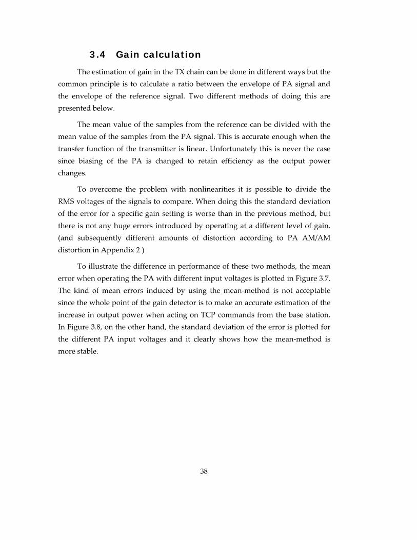
The estimation of gain in the TX chain can be done in different ways but the common principle is to calculate a ratio between the envelope of PA signal and the envelope of the reference signal. Two different methods of doing this are presented below.
The mean value of the samples from the reference can be divided with the mean value of the samples from the PA signal. This is accurate enough when the transfer function of the transmitter is linear. Unfortunately this is never the case since biasing of the PA is changed to retain efficiency as the output power changes.
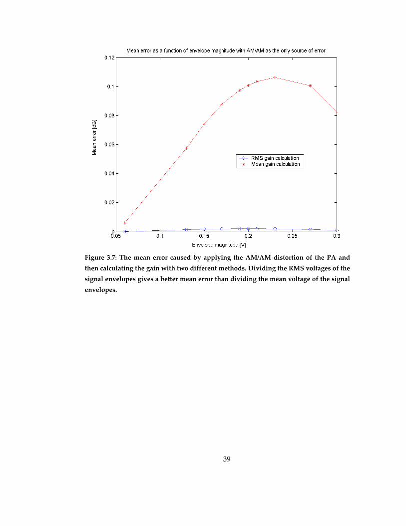
To overcome the problem with nonlinearities it is possible to divide the RMS voltages of the signals to compare. When doing this the standard deviation of the error for a specific gain setting is worse than in the previous method, but there is not any huge errors introduced by operating at a different level of gain. (and subsequently different amounts of distortion according to PA AM/AM distortion in Appendix 2 )
To illustrate the difference in performance of these two methods, the mean error when operating the PA with different input voltages is plotted in Figure 3.7. The kind of mean errors induced by using the mean‐method is not acceptable since the whole point of the gain detector is to make an accurate estimation of the increase in output power when acting on TCP commands from the base station. In Figure 3.8, on the other hand, the standard deviation of the error is plotted for the different PA input voltages and it clearly shows how the mean‐method is more stable.
39
Figure 3.7: The mean error caused by applying the AM/AM distortion of the PA and then calculating the gain with two different methods. Dividing the RMS voltages of the signal envelopes gives a better mean error than dividing the mean voltage of the signal envelopes.
40
Figure 3.8: Standard deviation of error from distortion for two different ways of estimating the TX gain.
3.5 Reducing impact of distortion
Distortion causes problems when the signal is so badly represented as it is in this case. Gain calculation will be very much dependent on what part of the waveform happens to be represented by the samples (
Figure 3.9).

41
Figure 3.9: Two waveforms compared side by side. One shows the unmodified Q signal and the other the Q signal that has been subjected to third order harmonic distortion. Calculating the gain between the two waveforms is not trivial because the calculated gain depends on which samples are used. Gain 2 in the figure would be significantly higher than Gain 1. Using the sub‐sampled PA signal means that one risks over‐representation of one specific y‐level of the signal. For example; the few samples that are measured could happen to over‐represent the peaks, in which case the gain would be over‐estimated. By removing some of the samples at the peaks this could be avoided to some degree.
Original w aveform
-4
-2
0
2
4
0 2 4 6 8 10 12
time
volta
ge
Original w aveform
Distorted w aveform
-6
-4
-2
0
2
4
6
8
0 2 4 6 8 10 12
time
volta
ge
Distorted w aveform
Gain 2
Gain 1
42
3.5.1 Reduced sample collection
To remedy the imperfections introduced into the gain calculations by PA nonlinearities, a scheme has been developed where the sample collection spread over the y‐axis is modified by removing elements on y‐levels where there is an over‐representation. If the signal would have been sampled in 52 MHz as it is in the reference, the correct RMS voltage would be calculated and the correct power gain could be calculated from this. Assuming that fewer samples were to be used than originally present in the reference and one wanted to calculate the RMS voltage correctly, one would have to modify the distribution along the y‐axis to resemble the distribution of the reference signal.
To apply this in practice the samples of the reference slice are sorted into three different baskets according to value. After time alignment and down‐sampling the same thing is repeated. Some of the samples in the down‐sampled reference and PA signal (typically 30 %) are now removed to imitate the distribution of the full resolution reference.
While this method greatly improves the performance with respect to distortion, it makes all stochastic errors worse by removing valid data.
3.5.2 Extended sample collection
To reach the same performance as just described without removing important samples, one can interpolate in the baskets where there are too few samples. The effect will be that the RMS calculation will be more dependent on those samples that are used for linear interpolation. The goal is to retain the algorithms ability to handle noise, time mismatch and phase noise. In Figure 4.5 on page 53 the two methods are pitted against each other and the unmodified sample collection with respect to their ability to handle distortion. The suppression of noise for the three methods is compared in

43
Table 5. This comparison shows that the removal of samples causes unnecessary errors when other error sources than distortion are added.
44
Table 5: The error of the gain calculation when noise has been added to the envelope. The noise was Gaussian with a standard deviation of 0.02.
Standard deviation
of error
Original Removed samples Added samples
0.0506 0.0562 0.0515
3.5.3 Distorting the reference
Using the sampled data it is possible to create an AM/AM distortion polynomial. With this the reference signal could be pre‐distorted and its RMS compared to that of the original reference. Doing this in hardware would be quite a challenge and it has thus not been investigated further.
3.5.4 Conclusion
The method of increasing the number of samples by interpolation improves performance without affecting the stochastic errors which is desirable. Simulations indicate that the gain estimation is improved with this solution. Considering low acquisition time is sought it is preferable to implement the method that adds samples.
3.6 Increasing sample-rate or slice length
The number of samples used to make the comparison between the reference signal and the PA signal can affect the influence of the error introduced in each sample. The errors are stochastic, so using a large number of samples will give a mean value that is closer to the real one1. Increasing the time used for gain estimation might not be possible because the power control algorithm expects results on regular, fairly short, intervals. Instead a similar improvement could be accomplished by increasing the ADC sample‐rate (Figure 3.10).
1 The real value is the result with perfect time alignment.

45
Figure 3.10: Standard deviation of the error when estimating the gain for three different ADC sample‐rates. The only source of error used is imperfect time alignment. It is possible to increase performance by increasing sample‐rate if acquisition time is kept constant.
46
3.7 DC compensation
The signal that reaches the ADC has a DC component which origins from the receiver chain and has thus to be eliminated. The amount of DC may vary over time and that is why it is important to regularly make an accurate estimation of it before performing the elimination routine. The main idea is to calculate a mean value of the incoming samples and subtract it from the signal. The chosen method works by keeping the mean value of a number of recently processed slices saved. Since the DC from the mixers is amplified by the VGA, which changes along with TX‐gain settings, this is compensated for.
1. Gather a slice and calculate mean value of it.
2. Use currently set VGA gain to compensate for offset due to amplification.
3. Save the compensated mean value of the slice to the DC buffer.
4. Calculate mean value of the DC buffer.
5. Multiply the mean with the current VGA gain.
6. Subtract the mean value from the slice and proceed to calculate the gain.
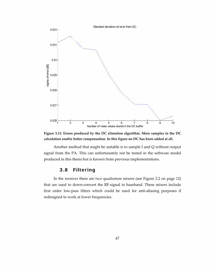
The longer the DC buffer is, the better the DC estimation will be unless the offset variation in the input signal is too severe. This would make the previous mean values useless for the next DC calculation. The buffer length is set according to tolerated error. Figure 3.11 shows the error versus number of samples used for DC estimation. The gain compensation is making it possible to make use of previously collected data if a gain step would occur. Other effects that might change the DC over time are harder to compensate for. The amount of DC that can be tolerated is around one percent which is shown in chapter 4.7. Fortunately the time alignment algorithm can handle up to 150% DC in relation to envelope amplitude.
47
Figure 3.11: Errors produced by the DC elimation algorithm. More samples in the DC calculation enable better compensation. In this figure no DC has been added at all.
Another method that might be suitable is to sample I and Q without output signal from the PA. This can unfortunately not be tested in the software model produced in this thesis but is known from previous implementations.
3.8 Filtering
In the receiver there are two quadrature mixers (see Figure 2.2 on page 12) that are used to down‐convert the RF‐signal to baseband. These mixers include first order low‐pass filters which could be used for anti‐aliasing purposes if redesigned to work at lower frequencies.

48
The error of the gain estimation is dependent of the difference in voltage between the two nearly time aligned samples. Low pass filtering the signals, and thereby decreasing high frequency content, would result in signals that vary less over time and this would decrease the error caused by imperfect time alignment. The filters would then have to be compensated for in the digital domain by applying similar FIR filters to the reference signal. The mismatch between the analog and digital filters would introduce new errors which is a good reason to avoid this solution.
49
4. Impact of error sources
4.1 Impact of ADC quantization
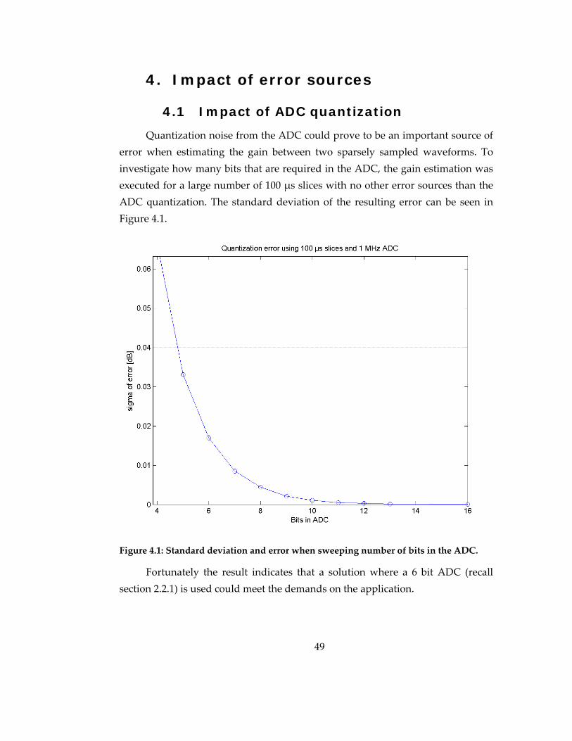
Quantization noise from the ADC could prove to be an important source of error when estimating the gain between two sparsely sampled waveforms. To investigate how many bits that are required in the ADC, the gain estimation was executed for a large number of 100 μs slices with no other error sources than the ADC quantization. The standard deviation of the resulting error can be seen in Figure 4.1.
Figure 4.1: Standard deviation and error when sweeping number of bits in the ADC.
Fortunately the result indicates that a solution where a 6 bit ADC (recall section 2.2.1) is used could meet the demands on the application.
50
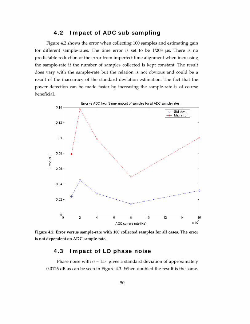
4.2 Impact of ADC sub sampling
Figure 4.2 shows the error when collecting 100 samples and estimating gain for different sample‐rates. The time error is set to be 1/208 μs. There is no predictable reduction of the error from imperfect time alignment when increasing the sample‐rate if the number of samples collected is kept constant. The result does vary with the sample‐rate but the relation is not obvious and could be a result of the inaccuracy of the standard deviation estimation. The fact that the power detection can be made faster by increasing the sample‐rate is of course beneficial.
Figure 4.2: Error versus sample‐rate with 100 collected samples for all cases. The error is not dependent on ADC sample‐rate.
4.3 Impact of LO phase noise
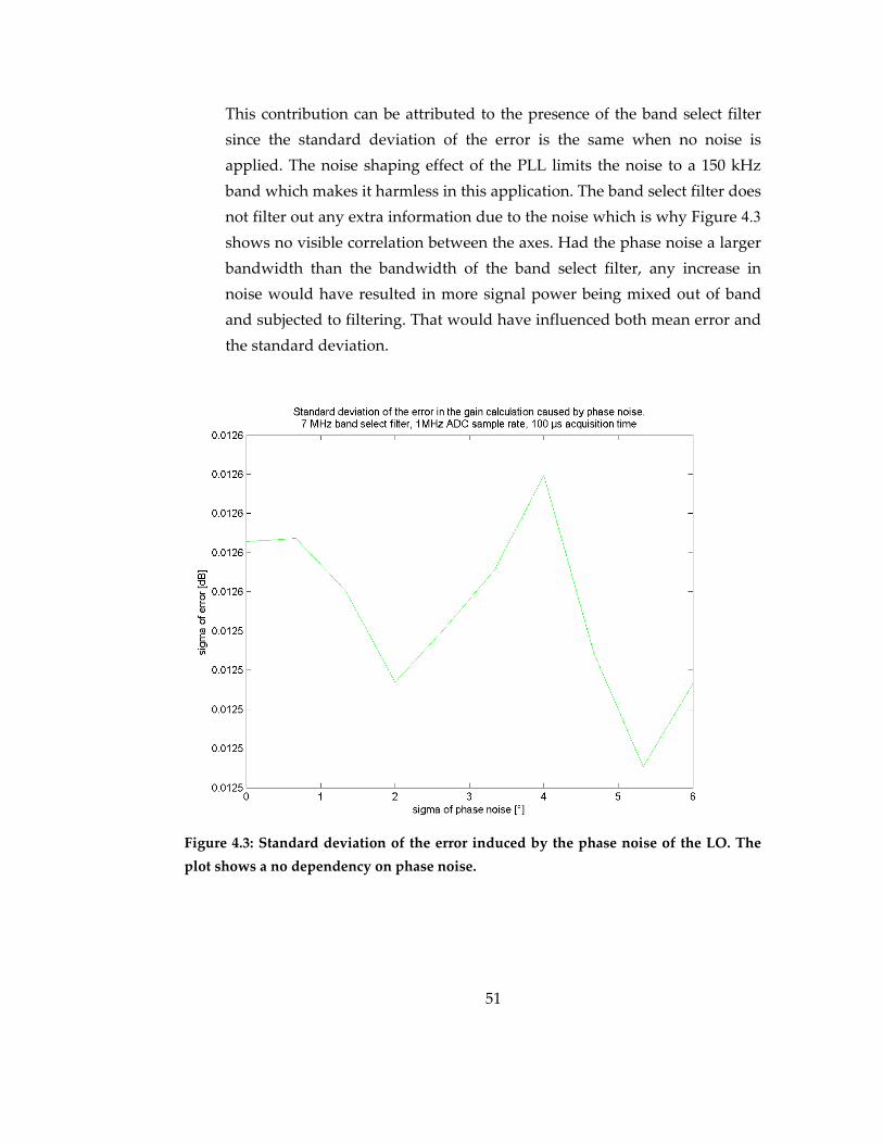
Phase noise with σ = 1.5° gives a standard deviation of approximately 0.0126 dB as can be seen in Figure 4.3. When doubled the result is the same.
51
This contribution can be attributed to the presence of the band select filter since the standard deviation of the error is the same when no noise is applied. The noise shaping effect of the PLL limits the noise to a 150 kHz band which makes it harmless in this application. The band select filter does not filter out any extra information due to the noise which is why Figure 4.3 shows no visible correlation between the axes. Had the phase noise a larger bandwidth than the bandwidth of the band select filter, any increase in noise would have resulted in more signal power being mixed out of band and subjected to filtering. That would have influenced both mean error and the standard deviation.
Figure 4.3: Standard deviation of the error induced by the phase noise of the LO. The plot shows a no dependency on phase noise.
52
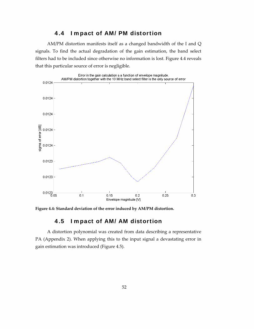
4.4 Impact of AM/PM distortion
AM/PM distortion manifests itself as a changed bandwidth of the I and Q signals. To find the actual degradation of the gain estimation, the band select filters had to be included since otherwise no information is lost. Figure 4.4 reveals that this particular source of error is negligible.
Figure 4.4: Standard deviation of the error induced by AM/PM distortion.
4.5 Impact of AM/AM distortion
A distortion polynomial was created from data describing a representative PA (Appendix 2). When applying this to the input signal a devastating error in gain estimation was introduced (Figure 4.5).
53
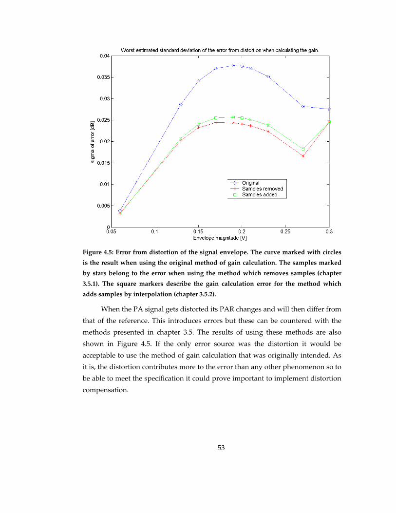
Figure 4.5: Error from distortion of the signal envelope. The curve marked with circles is the result when using the original method of gain calculation. The samples marked by stars belong to the error when using the method which removes samples (chapter 3.5.1). The square markers describe the gain calculation error for the method which adds samples by interpolation (chapter 3.5.2).
When the PA signal gets distorted its PAR changes and will then differ from that of the reference. This introduces errors but these can be countered with the methods presented in chapter 3.5. The results of using these methods are also shown in Figure 4.5. If the only error source was the distortion it would be acceptable to use the method of gain calculation that was originally intended. As it is, the distortion contributes more to the error than any other phenomenon so to be able to meet the specification it could prove important to implement distortion compensation.
54
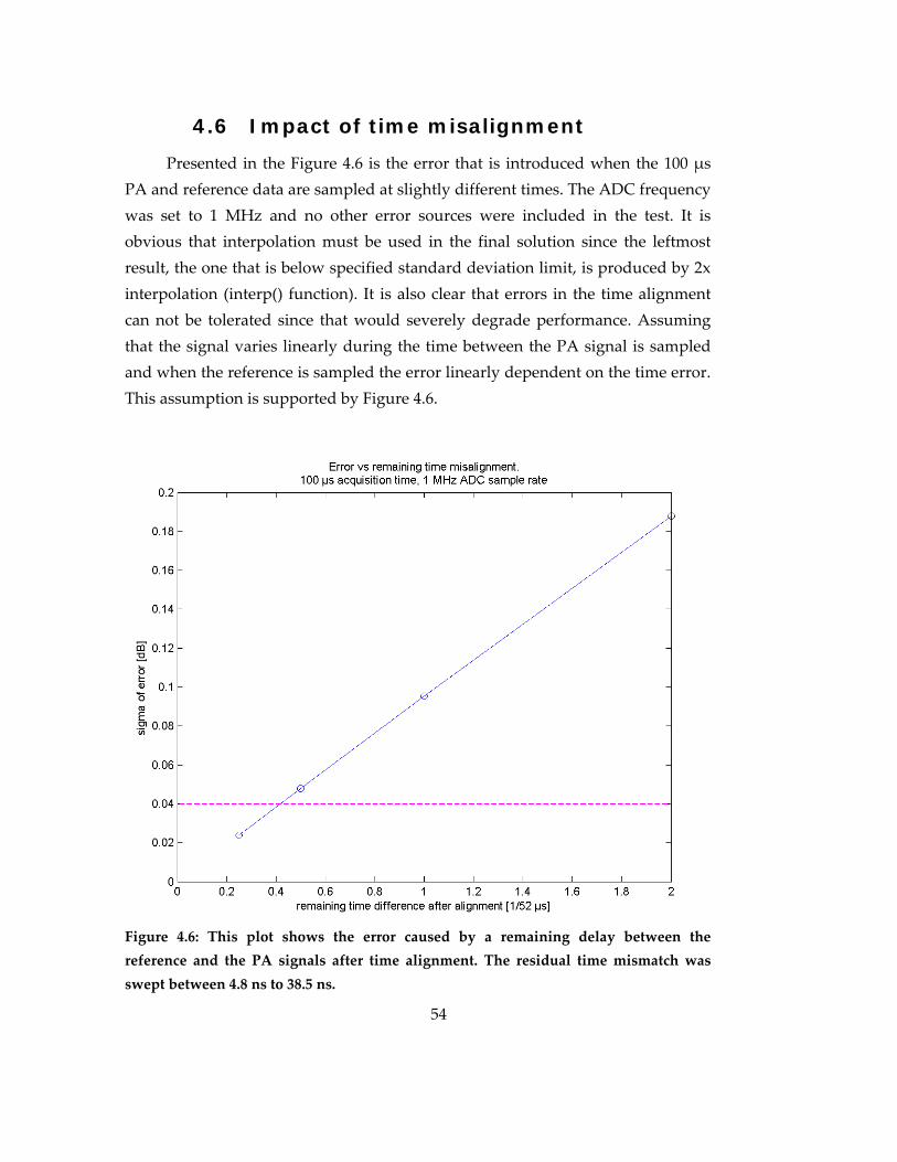
4.6 Impact of time misalignment
Presented in the Figure 4.6 is the error that is introduced when the 100 μs PA and reference data are sampled at slightly different times. The ADC frequency was set to 1 MHz and no other error sources were included in the test. It is obvious that interpolation must be used in the final solution since the leftmost result, the one that is below specified standard deviation limit, is produced by 2x interpolation (interp() function). It is also clear that errors in the time alignment can not be tolerated since that would severely degrade performance. Assuming that the signal varies linearly during the time between the PA signal is sampled and when the reference is sampled the error linearly dependent on the time error. This assumption is supported by Figure 4.6.
Figure 4.6: This plot shows the error caused by a remaining delay between the reference and the PA signals after time alignment. The residual time mismatch was swept between 4.8 ns to 38.5 ns.
55
4.7 Impact of DC
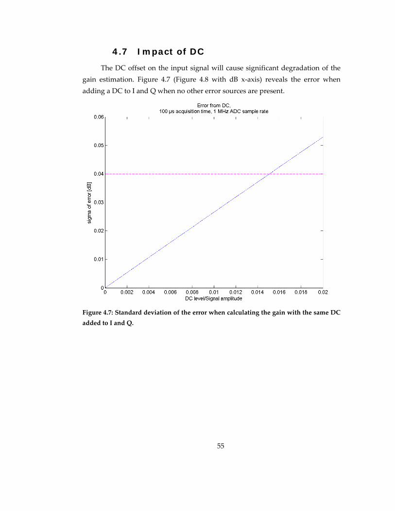
The DC offset on the input signal will cause significant degradation of the gain estimation. Figure 4.7 (Figure 4.8 with dB x‐axis) reveals the error when adding a DC to I and Q when no other error sources are present.
Figure 4.7: Standard deviation of the error when calculating the gain with the same DC added to I and Q.
56
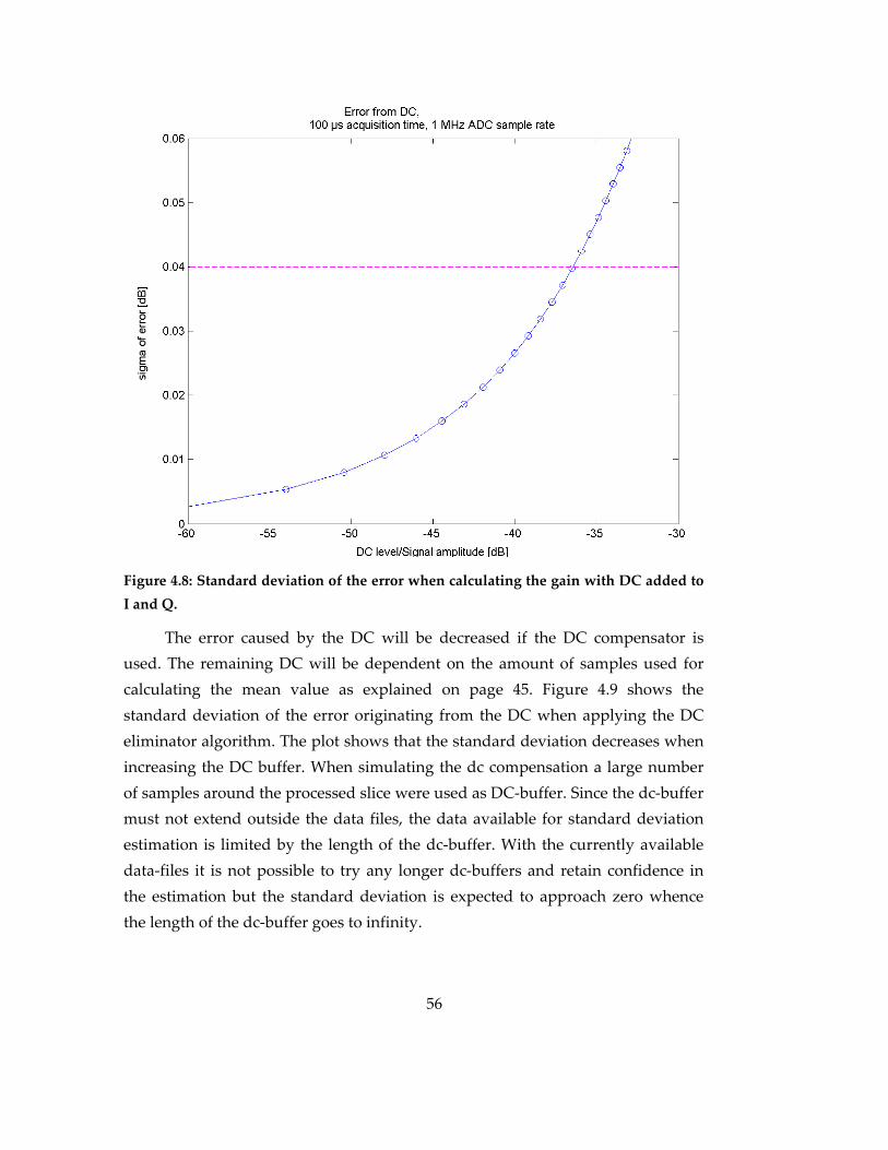
Figure 4.8: Standard deviation of the error when calculating the gain with DC added to I and Q.
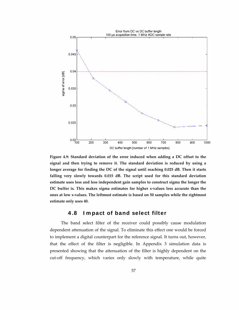
The error caused by the DC will be decreased if the DC compensator is used. The remaining DC will be dependent on the amount of samples used for calculating the mean value as explained on page 45. Figure 4.9 shows the standard deviation of the error originating from the DC when applying the DC eliminator algorithm. The plot shows that the standard deviation decreases when increasing the DC buffer. When simulating the dc compensation a large number of samples around the processed slice were used as DC‐buffer. Since the dc‐buffer must not extend outside the data files, the data available for standard deviation estimation is limited by the length of the dc‐buffer. With the currently available data‐files it is not possible to try any longer dc‐buffers and retain confidence in the estimation but the standard deviation is expected to approach zero whence the length of the dc‐buffer goes to infinity.
57
Figure 4.9: Standard deviation of the error induced when adding a DC offset to the signal and then trying to remove it. The standard deviation is reduced by using a longer average for finding the DC of the signal until reaching 0.025 dB. Then it starts falling very slowly towards 0.015 dB. The script used for this standard deviation estimate uses less and less independent gain samples to construct sigma the longer the DC buffer is. This makes sigma estimates for higher x‐values less accurate than the ones at low x‐values. The leftmost estimate is based on 50 samples while the rightmost estimate only uses 40.
4.8 Impact of band select filter
The band select filter of the receiver could possibly cause modulation dependent attenuation of the signal. To eliminate this effect one would be forced to implement a digital counterpart for the reference signal. It turns out, however, that the effect of the filter is negligible. In Appendix 3 simulation data is presented showing that the attenuation of the filter is highly dependent on the cut‐off frequency, which varies only slowly with temperature, while quite

58
unaffected by changes in modulation. The largest difference in attenuation occurs for the lowest cut‐off frequency when comparing the Rmc122 and WcAclr1Cm data files. The difference amounts to 0.0016 dB which can be considered low.
4.9 Impact of I/Q phase shift
Small delays in the PA and other blocks can rotate the constellation diagram randomly which translates to I and Q signals that are entirely different from the references. FFT of the signal before and after phase shift confirms that for high frequency noise there is a significant change (Appendix 1) but tests show that no errors are induced by this.

59
5. Proposed solution
Because of the low sample‐rate of the GenADC the solution needs to compare a maximum of 100 samples with corresponding samples of the reference signal to calculate the gain. An acquisition time longer than this is not acceptable. Time alignment is crucial and will be performed by oversampling the reference signal to 104 MHz and then calculating the mean square of the difference of the two signals for different time lags as described in chapter 3.3.5.
The overlapping segments of the time aligned vectors (the reference down‐sampled to 1 MHz) will have their distribution along the y‐axis modified to resemble the distribution of the full resolution reference signal. The purpose is to counter the impact of distortion and it will be done by interpolation in order not to loose information which is valuable to suppress noise. It is arguable that the sample removal method should be used since it is slightly less complex and deliver accurate enough results. Considering that the increased performance could be traded for shortened acquisition time however, it is advisable to make the effort to implement the interpolation.
The RMS voltage of the modified overlapping signals will be divided to acquire the gain from WFG to the digital part of the power detector. The gain will be compensated for the influence of the analog detector blocks and then used to estimate the output power from the known power of the WFG output.
As mentioned above, the sample collection will be cleverly expanded by interpolation to compensate for distortion. The claim that this method is superior is based on somewhat unreliable observations. No statistical analysis has been made to support this assumption. In order to support such a claim one would need to show a significant failure to meet specification for the two methods not chosen and a standard deviation estimate significantly below specification for the chosen method. The amount of data available for testing does not allow this. There is in fact not enough data to show that the results of the different methods are significantly different.
100 μs acquisition time is used to meet specification after an arbitrary step in gain. If a small step in gain is performed however, such would be the case

60
when correcting for an error in a previous gain change, a portion of the old data could be kept and still get a detected power that is useful.
5.1 Errors when everything is combined
With the intention of choosing gain calculation method, the final testbench was produced. The test included
• TXLpf at its lowest cut‐off frequency
• Transmitter and receiver mixer phase noise of N[0,3°] with 150 kHz bandwidth.
• PA AM/PM and AM/AM distortion from input amplitude of 0.2 V resulting in quite a lot of change in the signal.
• No DC offset but the removal algorithm is turned on, removing the average of 8 slices of 100 samples.
• Band select filter at 7 MHz.
• ADC quantization corresponding to a resolution of 6 bits. ADC sample‐rate of 1 MHz.
61
5.1.1 Results of different files
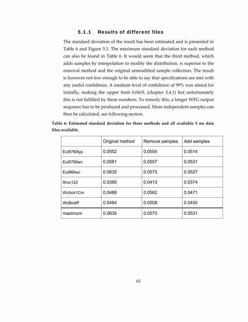
The standard deviation of the result has been estimated and is presented in Table 6 and Figure 5.1. The maximum standard deviation for each method can also be found in Table 6. It would seem that the third method, which adds samples by interpolation to modify the distribution, is superior to the removal method and the original unmodified sample collection. The result is however not low enough to be able to say that specifications are met with any useful confidence. A medium level of confidence of 99% was aimed for initially, making the upper limit 0,0419, (chapter 2.4.1) but unfortunately this is not fulfilled by these numbers. To remedy this, a longer WFG output sequence has to be produced and processed. More independent samples can then be calculated, see following section.
Table 6: Estimated standard deviation for three methods and all available 5 ms data files available.
Original method Remove samples Add samples
Eul5760typ 0.0552 0.0554 0.0514
Eul5760wc 0.0561 0.0557 0.0531
Eul960wc 0.0635 0.0573 0.0527
Rmc122 0.0395 0.0413 0.0374
WcAclr1Cm 0.0488 0.0562 0.0471
WcBodiff 0.0484 0.0508 0.0455
maximum 0.0635 0.0573 0.0531
62
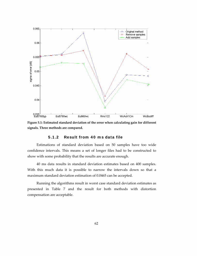
Figure 5.1: Estimated standard deviation of the error when calculating gain for different signals. Three methods are compared.
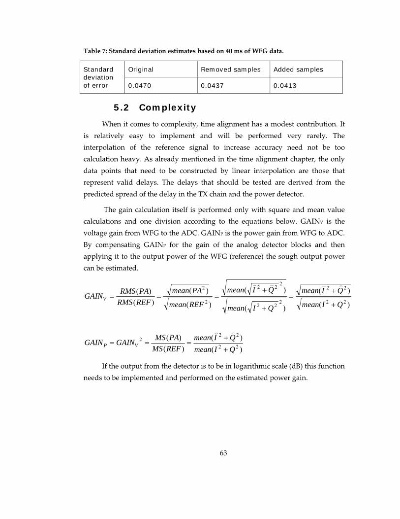
5.1.2 Result from 40 ms data file
Estimations of standard deviation based on 50 samples have too wide confidence intervals. This means a set of longer files had to be constructed to show with some probability that the results are accurate enough.
40 ms data results in standard deviation estimates based on 400 samples. With this much data it is possible to narrow the intervals down so that a maximum standard deviation estimation of 0.0465 can be accepted.
Running the algorithms result in worst case standard deviation estimates as presented in Table 7 and the result for both methods with distortion compensation are acceptable.
63
Table 7: Standard deviation estimates based on 40 ms of WFG data.
Standard deviation of error
Original Removed samples Added samples
0.0470 0.0437 0.0413
5.2 Complexity
When it comes to complexity, time alignment has a modest contribution. It is relatively easy to implement and will be performed very rarely. The interpolation of the reference signal to increase accuracy need not be too calculation heavy. As already mentioned in the time alignment chapter, the only data points that need to be constructed by linear interpolation are those that represent valid delays. The delays that should be tested are derived from the predicted spread of the delay in the TX chain and the power detector.
The gain calculation itself is performed only with square and mean value calculations and one division according to the equations below. GAINV is the voltage gain from WFG to the ADC. GAINP is the power gain from WFG to ADC. By compensating GAINP for the gain of the analog detector blocks and then applying it to the output power of the WFG (reference) the sough output power can be estimated.
)(
)(
)(
)(
)(
)()(
)(22
22
222
222
2
2
QImean
QImean
QImean
QImean
REFmean
PAmeanREFRMSPARMSGAINV
+
+=
+
+===
))))
)()(
)()(
22
222
QImeanQImean
REFMSPAMSGAINGAIN VP
++
===))
If the output from the detector is to be in logarithmic scale (dB) this function needs to be implemented and performed on the estimated power gain.

64
The distortion compensation method is the single most complicated part of the whole solution. The fact that the number of samples on each level has to be calculated requires a lot of calculations since two comparisons are needed for each reference sample. This can be an ongoing process as the data is collected. A measure of the distribution for the the downsampled reference can be created at the same time by just using every 52nd value. This leaves the problem of sorting the down‐sampled reference data (and with it the PA‐data). With a good algorithm for sorting that makes use of parallelism and the ability to start calculations before all data has been acquired it should be possible to deliver power estimations on time.
The DC compensation technique used in the proposed solution has a fairly low arithmetic complexity. The only work done is calculating the mean value of the incoming data and this should pose no problem.

65
6. Conclusion
The solution proposed in chapter 5 meets the specification. The complexity of the solution is reasonable and should be possible to implement using a low cost ADC. Assuming that the digital hardware added has negligible power consumption, the solution will be competitive when it comes to energy conservation as well. It is still possible that no means are necessary to compensate for distortion, but it has been made likely that such compensation is possible and that the complexity of that algorithm is acceptable.
The required time alignment can be performed by using a mere 100 samples and need not be run at tight time intervals due to the slow‐changing time delay of the TX‐chain.
Regarding the sources of errors there are some sources that have more effect than others. The worst is PA distortion and time misalignment and naturally the biggest efforts have been made to compensate for these. ADC quantization noise is also a significant contributor to the overall error.
6.1 The competition
In “Single‐Chip Tri‐Band WCDMA/HSDPA Transceiver without External SAW Filters and with Integrated TX Power Control” [16] has been demonstrated a solution similar to the one presented in this paper. Part of the RF signal is redirected and mixed‐down to baseband for digital conversion. The sample‐rate of the proposed ADC is 30 MHz and the transmitter input signal is used as a reference to remove modulation dependency. RMS values with an accuracy of ±0.3 dB can be delivered with a 15 μs interval [16] which means that 450 samples are used for the power estimation. The solution proposed in this report compares well with the one described above. Acquisition time is longer, which is a drawback, but the limited silicon area used and lower current consumption will be a great advantage.
6.2 Future work
The solution in its current form leaves some things to be solved in the future. Much of the remaining work is practical like implementing the algorithm
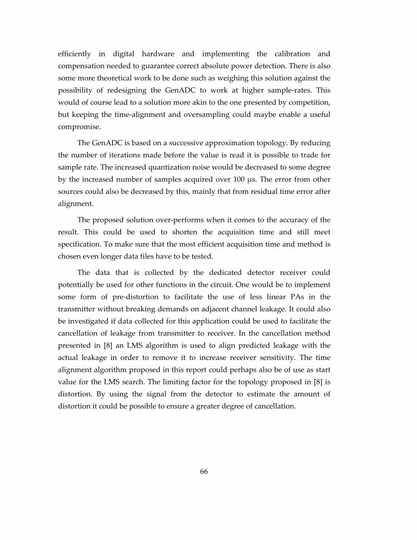
66
efficiently in digital hardware and implementing the calibration and compensation needed to guarantee correct absolute power detection. There is also some more theoretical work to be done such as weighing this solution against the possibility of redesigning the GenADC to work at higher sample‐rates. This would of course lead to a solution more akin to the one presented by competition, but keeping the time‐alignment and oversampling could maybe enable a useful compromise.
The GenADC is based on a successive approximation topology. By reducing the number of iterations made before the value is read it is possible to trade for sample rate. The increased quantization noise would be decreased to some degree by the increased number of samples acquired over 100 μs. The error from other sources could also be decreased by this, mainly that from residual time error after alignment.
The proposed solution over‐performs when it comes to the accuracy of the result. This could be used to shorten the acquisition time and still meet specification. To make sure that the most efficient acquisition time and method is chosen even longer data files have to be tested.
The data that is collected by the dedicated detector receiver could potentially be used for other functions in the circuit. One would be to implement some form of pre‐distortion to facilitate the use of less linear PAs in the transmitter without breaking demands on adjacent channel leakage. It could also be investigated if data collected for this application could be used to facilitate the cancellation of leakage from transmitter to receiver. In the cancellation method presented in [8] an LMS algorithm is used to align predicted leakage with the actual leakage in order to remove it to increase receiver sensitivity. The time alignment algorithm proposed in this report could perhaps also be of use as start value for the LMS search. The limiting factor for the topology proposed in [8] is distortion. By using the signal from the detector to estimate the amount of distortion it could be possible to ensure a greater degree of cancellation.

67
7. References
[1] TxTop Design book. Rev. PB1, 2007‐11‐23, page 23. Responsible author Magnus Nilsson. Ericsson internal.
[2] Control in Mobile Communication 2004, lecture 3, Bo Bernhardsson, http://www.control.lth.se/~bob/lecture03.pdf, (2004‐11‐10)
[3] 3rd Generation Partnership Project; Technical Specification Group Radio Access Network; User Equipment (UE) radio transmission and reception (FDD), 25.101, (Release 8), page 18
[4] Requirements Specification for R15 Power Detector for WCDMA, 3/1056‐FCP 101 4745 Uen Rev D, page 9. Ericsson internal.
[5] Electronic communication techniques fifth edition, Paul H Young, Pearson Prentice Hall, ISBN nr: 0‐13‐048285‐4, page 149 and 652.
[6] IP: R15 WCDMA TX Power control internal algorithm (PIA), 1/159 41‐CNH 160 4070 Uen. Ericsson Internal.
[7] Gain control accuracy in the R15 TX chain, 25/0363‐FCP 101 3392 Uen, page 3. Ericsson Internal.
[8] Digital Interference Cancellation in a Full Duplex System. Master thesis by Thomas Ahlström, Claes Bengtsson, page 56.
[9] Transmitter Budget; Spread Sheet for Power Control, Björn Gustavsson, 2007‐08‐08, Sheets: Closed loop stabilization time, Data. Ericsson Internal.
[10] IP: R15 WCDMA TX Power control internal algorithm (PIA). Rev PA2., 1/159 41‐CNH 160 4070 Uen, page 7. Ericsson Internal.
[11] LMV221 50 MHz to 3.5 GHz 40 dB Logarithmic Power Detector for CDMA and WCDMA, page 20, http://www.national.com/ds.cgi/LM/LMV221.pdf

68
[12] Statistikteori med tillämpningar, Gunnar Blom, Björn Holmquist, 1998, page 100. ISBN: 91‐44‐00323‐4.
[13] Distcalc.exe v1.2. A program by H. Lohninger. TU Wien.
[14] Digital signal processing – A Computer‐Based Approach, Second Edition, Sanjit K. Mitra, International Edition, Mc GrawHill, page 89 and 302.
[15] Matlab 6.5.0.180913a Release 13, Signal Processing Toolbox, interp help
[16] Single‐Chip Tri‐Band WCDMA/HSDPA Transceiver without External SAW Filters and with Integrated TX Power Control, Bernard Tenbroek, Jonathan Strange, Dimitris Nalbantis, Christopher Jones, Paul Fowers, Steve Brett, Christophe Beghein, Federico Beffa, (2008‐02‐05)
[17] Wireless Digital Communications by Andreas F. Molisch 2004‐03‐15. Chapter 17, page 3.
[18] Introduction To Mobile Telephony, Tech Support AB 2005 2.0. Pages 10 and 11.
[19] 3rd Generation Partnership Project, Technical Specification Group Radio Access Network; Spreading and modulation (FDD), (release 8). 3GPP TS 25.213 V7.3.0 (2007‐09).
[20] Which ADC Architecture Is Right for Your Application?, Walt Kester, Analog Dialogue 39‐06, (2005‐06), page 5. http://www.analog.com/library/analogDialogue/archives/39‐06/architecture.pdf
[21] E‐mail from Fredrik Tillman to Robert Carlzén. (2008‐01‐08)
[22] Ericsson Mobile Platform U360, WCDMA transmitter training, slide 8. Ericsson Internal
[23] Conversation with Magnus Nilsson (ECSMSNN)

I
Appendix 1
Figure 7.1 shows the spectrum of Q in different parts of the TX chain compared to Q taken directly after the WFG. The effect on I is very similar which is why this is not included. Figure 7.2 shows the effects of the analog detector blocks. The block schematics are drawn in a simplified manner with only one block for I and Q processing instead of two individual. The conversion to radio frequency has been left out as well any amplification which makes it easier to see the effect on the frequency content of the signal. Because of limited length of the tested signal the noise floor is quite high which makes it difficult to see the filtering effects.
1. Reference signal. 2. A 4 MHz third order low pass filter has been applied. 3. White phase noise white a standard deviation of 3° originating from the
mixer has been added. 4. The signal is amplified to reach the level which will be most distorted in
the PA. This amplification is removed after AM/AM and PM/AM distortion is added to make the plots comparable.
5. A phase angle of 2 radians and a phase noise with a standard deviation of 3° has been added to the signal.
6. A 10 MHz first order low pass filter has been applied. 7. The ADC has quantized the signal to 6 bit representation and sampled
down to 1 MHz. All that is left is white noise.
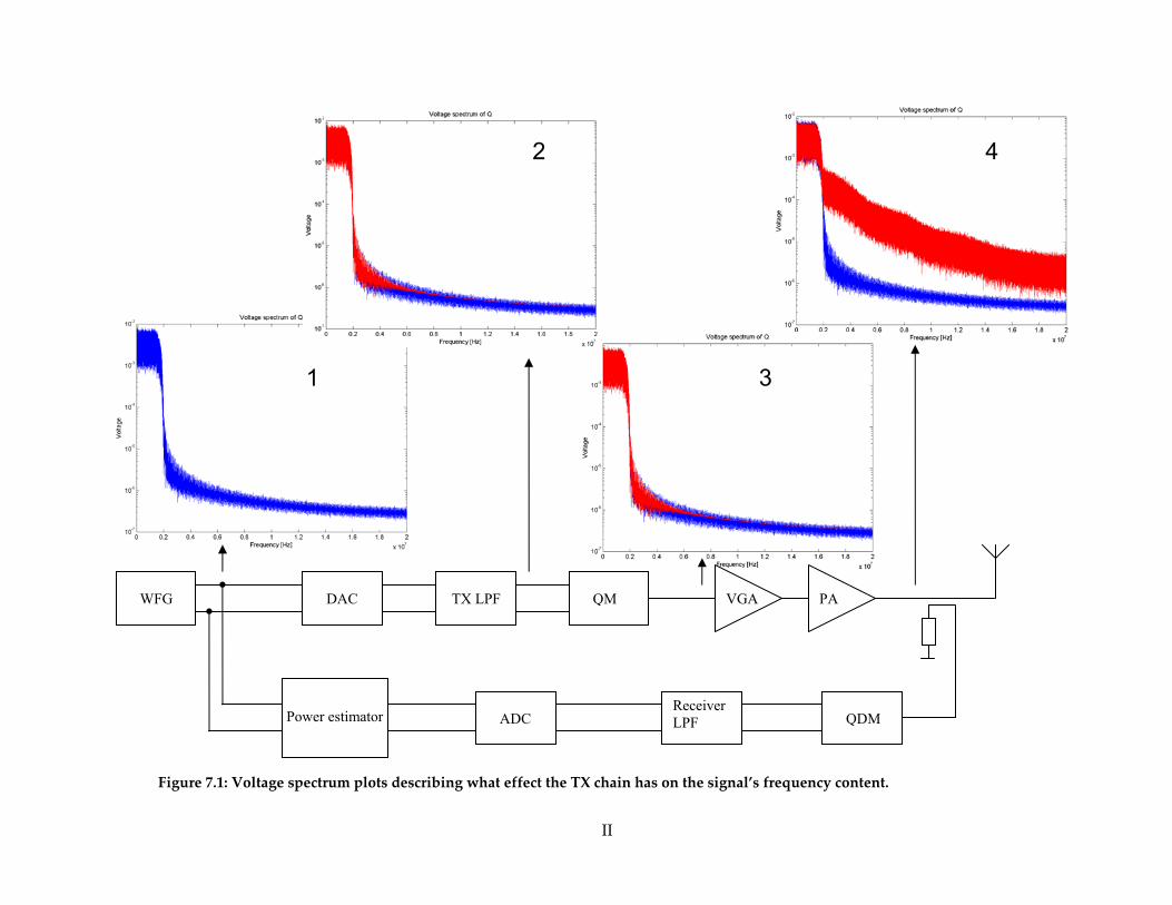
II
Figure 7.1: Voltage spectrum plots describing what effect the TX chain has on the signal’s frequency content.
WFG DAC VGA
QDMADC
QMTX LPF
Power estimator Receiver LPF
PA
1
2
3
4
III
Figure 7.2: Voltage spectrum plots describing what effect the analog blocks of the detector have on the signal’s frequency content.
WFG DAC VGA
QDMADC
QMTX LPF
Power estimator Receiver LPF
PA
5 6 7
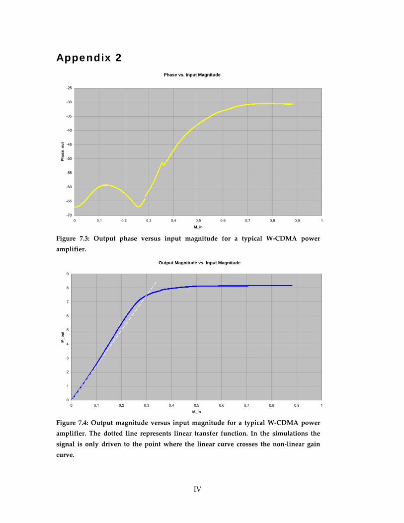
IV
Appendix 2 Phase vs. Input Magnitude
-70
-65
-60
-55
-50
-45
-40
-35
-30
-25
0 0,1 0,2 0,3 0,4 0,5 0,6 0,7 0,8 0,9 1
M_in
Phas
e_ou
t
Figure 7.3: Output phase versus input magnitude for a typical W‐CDMA power amplifier.
Output Magnitude vs. Input Magnitude
0
1
2
3
4
5
6
7
8
9
0 0,1 0,2 0,3 0,4 0,5 0,6 0,7 0,8 0,9 1
M_in
M_o
ut
Figure 7.4: Output magnitude versus input magnitude for a typical W‐CDMA power amplifier. The dotted line represents linear transfer function. In the simulations the signal is only driven to the point where the linear curve crosses the non‐linear gain curve.
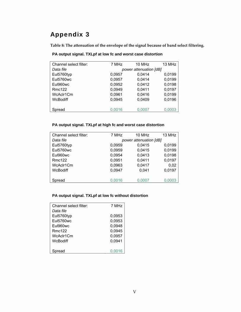
V
Appendix 3
Table 8: The attenuation of the envelope of the signal because of band select filtering.
PA output signal. TXLpf at low fc and worst case distortion Channel select filter: 7 MHz 10 MHz 13 MHz Data file power attenuation [dB] Eul5760typ 0,0957 0,0414 0,0199 Eul5760wc 0,0957 0,0414 0,0199 Eul960wc 0,0952 0,0412 0,0198 Rmc122 0,0949 0,0411 0,0197 WcAclr1Cm 0,0961 0,0416 0,0199 WcBodiff 0,0945 0,0409 0,0196 Spread 0,0016 0,0007 0,0003 PA output signal. TXLpf at high fc and worst case distortion Channel select filter: 7 MHz 10 MHz 13 MHz Data file power attenuation [dB] Eul5760typ 0,0959 0,0415 0,0199 Eul5760wc 0,0959 0,0415 0,0199 Eul960wc 0,0954 0,0413 0,0198 Rmc122 0,0951 0,0411 0,0197 WcAclr1Cm 0,0963 0,0417 0,02 WcBodiff 0,0947 0,041 0,0197 Spread 0,0016 0,0007 0,0003 PA output signal. TXLpf at low fc without distortion Channel select filter: 7 MHz Data file Eul5760typ 0,0953 Eul5760wc 0,0953 Eul960wc 0,0948 Rmc122 0,0945 WcAclr1Cm 0,0957 WcBodiff 0,0941 Spread 0,0016
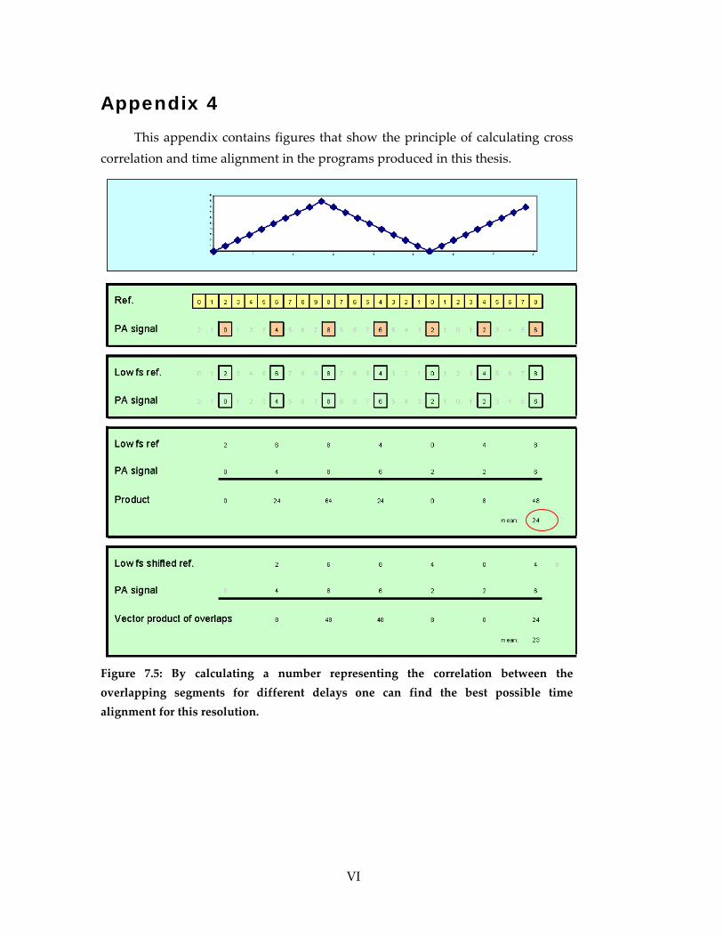
VI
Appendix 4
This appendix contains figures that show the principle of calculating cross correlation and time alignment in the programs produced in this thesis.
Figure 7.5: By calculating a number representing the correlation between the overlapping segments for different delays one can find the best possible time alignment for this resolution.
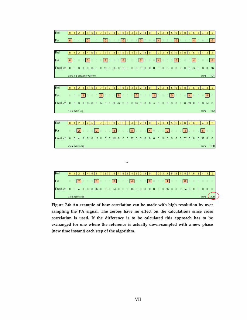
VII
Figure 7.6: An example of how correlation can be made with high resolution by over sampling the PA signal. The zeroes have no effect on the calculations since cross correlation is used. If the difference is to be calculated this approach has to be exchanged for one where the reference is actually down‐sampled with a new phase (new time instant) each step of the algorithm.
