digital signal processor. (rev. b) - texas instruments
TRANSCRIPT

SM320F2812-HTDigital Signal Processor
Data Manual
PRODUCTION DATA information is current as of publication date.Products conform to specifications per the terms of the TexasInstruments standard warranty. Production processing does notnecessarily include testing of all parameters.
Literature Number: SGUS062B
June 2009–Revised June 2011

SM320F2812-HT
SGUS062B–JUNE 2009–REVISED JUNE 2011 www.ti.com
Contents1 Features ........................................................................................................................... 11
1.1 SUPPORTS EXTREME TEMPERATURE APPLICATIONS ......................................................... 122 Introduction ...................................................................................................................... 13
2.1 Description ................................................................................................................. 13
2.2 Device Summary .......................................................................................................... 13
2.3 Die Layout .................................................................................................................. 14
2.4 Pin Assignments ........................................................................................................... 15
2.5 Signal Descriptions ........................................................................................................ 163 Functional Overview .......................................................................................................... 25
3.1 Memory Map ............................................................................................................... 263.2 Brief Descriptions .......................................................................................................... 29
3.2.1 C28x CPU ....................................................................................................... 29
3.2.2 Memory Bus (Harvard Bus Architecture) .................................................................... 29
3.2.3 Peripheral Bus .................................................................................................. 29
3.2.4 Real-Time JTAG and Analysis ................................................................................ 29
3.2.5 External Interface (XINTF) .................................................................................... 30
3.2.6 Flash ............................................................................................................. 30
3.2.7 L0, L1, H0 SARAMs ............................................................................................ 30
3.2.8 Boot ROM ....................................................................................................... 30
3.2.9 Security .......................................................................................................... 31
3.2.10 Peripheral Interrupt Expansion (PIE) Block ................................................................. 32
3.2.11 External Interrupts (XINT1, XINT2, XINT13, XNMI) ........................................................ 32
3.2.12 Oscillator and PLL .............................................................................................. 32
3.2.13 Watchdog ........................................................................................................ 32
3.2.14 Peripheral Clocking ............................................................................................. 32
3.2.15 Low-Power Modes .............................................................................................. 32
3.2.16 Peripheral Frames 0, 1, 2 (PFn) .............................................................................. 33
3.2.17 General-Purpose Input/Output (GPIO) Multiplexer ......................................................... 33
3.2.18 32-Bit CPU Timers (0, 1, 2) ................................................................................... 33
3.2.19 Control Peripherals ............................................................................................. 33
3.2.20 Serial Port Peripherals ......................................................................................... 34
3.3 Register Map ............................................................................................................... 34
3.4 Device Emulation Registers .............................................................................................. 373.5 External Interface, XINTF ................................................................................................ 37
3.5.1 Timing Registers ................................................................................................ 39
3.5.2 XREVISION Register ........................................................................................... 393.6 Interrupts .................................................................................................................... 40
3.6.1 External Interrupts .............................................................................................. 43
3.7 System Control ............................................................................................................ 443.8 OSC and PLL Block ....................................................................................................... 46
3.8.1 Loss of Input Clock ............................................................................................. 47
3.9 PLL-Based Clock Module ................................................................................................ 47
3.10 External Reference Oscillator Clock Option ........................................................................... 47
3.11 Watchdog Block ........................................................................................................... 48
3.12 Low-Power Modes Block ................................................................................................. 49
2 Contents Copyright © 2009–2011, Texas Instruments Incorporated

SM320F2812-HT
www.ti.com SGUS062B–JUNE 2009–REVISED JUNE 2011
4 Peripherals ....................................................................................................................... 504.1 32-Bit CPU-Timers 0/1/2 ................................................................................................. 504.2 Event Manager Modules (EVA, EVB) ................................................................................... 53
4.2.1 General-Purpose (GP) Timers ................................................................................ 56
4.2.2 Full-Compare Units ............................................................................................. 56
4.2.3 Programmable Deadband Generator ........................................................................ 56
4.2.4 PWM Waveform Generation .................................................................................. 56
4.2.5 Double Update PWM Mode ................................................................................... 56
4.2.6 PWM Characteristics ........................................................................................... 57
4.2.7 Capture Unit ..................................................................................................... 57
4.2.8 Quadrature-Encoder Pulse (QEP) Circuit ................................................................... 57
4.2.9 External ADC Start-of-Conversion ........................................................................... 57
4.3 Enhanced Analog-to-Digital Converter (ADC) Module ............................................................... 58
4.4 Enhanced Controller Area Network (eCAN) Module .................................................................. 63
4.5 Multichannel Buffered Serial Port (McBSP) Module .................................................................. 67
4.6 Serial Communications Interface (SCI) Module ....................................................................... 71
4.7 Serial Peripheral Interface (SPI) Module ............................................................................... 74
4.8 GPIO MUX ................................................................................................................. 775 Development Support ........................................................................................................ 80
5.1 Device and Development Support Tool Nomenclature ............................................................... 80
5.2 Documentation Support ................................................................................................... 816 Electrical Specifications ..................................................................................................... 84
6.1 Absolute Maximum Ratings .............................................................................................. 84
6.2 Recommended Operating Conditions .................................................................................. 85
6.3 Electrical Characteristics ................................................................................................. 856.4 Current Consumption by Power-Supply Pins Over Recommended Operating Conditions During
Low-Power Modes at 150-MHz SYSCLKOUT ......................................................................... 87
6.5 Current Consumption Graphs ............................................................................................ 88
6.6 Reducing Current Consumption ......................................................................................... 89
6.7 Power Sequencing Requirements ....................................................................................... 89
6.8 Signal Transition Levels .................................................................................................. 91
6.9 Timing Parameter Symbology ........................................................................................... 92
6.10 General Notes on Timing Parameters .................................................................................. 92
6.11 Test Load Circuit .......................................................................................................... 92
6.12 Device Clock Table ........................................................................................................ 936.13 Clock Requirements and Characteristics ............................................................................... 93
6.13.1 Input Clock Requirements ..................................................................................... 93
6.13.2 Output Clock Characteristics .................................................................................. 94
6.14 Reset Timing ............................................................................................................... 95
6.15 Low-Power Mode Wakeup Timing ...................................................................................... 996.16 Event Manager Interface ................................................................................................ 103
6.16.1 PWM Timing ................................................................................................... 103
6.16.2 Interrupt Timing ................................................................................................ 105
6.17 General-Purpose Input/Output (GPIO) – Output Timing ............................................................ 106
6.18 General-Purpose Input/Output (GPIO) – Input Timing .............................................................. 107
6.19 SPI Master Mode Timing ................................................................................................ 108
6.20 SPI Slave Mode Timing ................................................................................................. 112
Copyright © 2009–2011, Texas Instruments Incorporated Contents 3

SM320F2812-HT
SGUS062B–JUNE 2009–REVISED JUNE 2011 www.ti.com
6.21 External Interface (XINTF) Timing ..................................................................................... 114
6.22 XINTF Signal Alignment to XCLKOUT ................................................................................ 118
6.23 External Interface Read Timing ........................................................................................ 119
6.24 External Interface Write Timing ........................................................................................ 120
6.25 External Interface Ready-on-Read Timing With One External Wait State ....................................... 122
6.26 External Interface Ready-on-Write Timing With One External Wait State ........................................ 125
6.27 XHOLD and XHOLDA ................................................................................................... 128
6.28 XHOLD/XHOLDA Timing ............................................................................................... 1296.29 On-Chip Analog-to-Digital Converter .................................................................................. 131
6.29.1 ADC Absolute Maximum Ratings ........................................................................... 131
6.29.2 ADC Electrical Characteristics Over Recommended Operating Conditions ........................... 132
6.29.3 Current Consumption for Different ADC Configurations (at 25-MHz ADCCLK) ...................... 133
6.29.4 ADC Power-Up Control Bit Timing .......................................................................... 1346.29.5 Detailed Description .......................................................................................... 135
6.29.5.1 Reference Voltage ................................................................................ 135
6.29.5.2 Analog Inputs ..................................................................................... 135
6.29.5.3 Converter .......................................................................................... 135
6.29.5.4 Conversion Modes ............................................................................... 135
6.29.6 Sequential Sampling Mode (Single Channel) (SMODE = 0) ............................................ 135
6.29.7 Simultaneous Sampling Mode (Dual-Channel) (SMODE = 1) .......................................... 1376.29.8 Definitions of Specifications and Terminology ............................................................. 138
6.29.8.1 Integral Nonlinearity .............................................................................. 138
6.29.8.2 Differential Nonlinearity .......................................................................... 138
6.29.8.3 Zero Offset ........................................................................................ 138
6.29.8.4 Gain Error ......................................................................................... 138
6.29.8.5 Signal-to-Noise Ratio + Distortion (SINAD) ................................................... 138
6.29.8.6 Effective Number of Bits (ENOB) ............................................................... 138
6.29.8.7 Total Harmonic Distortion (THD) ............................................................... 138
6.29.8.8 Spurious Free Dynamic Range (SFDR) ....................................................... 1386.30 Multichannel Buffered Serial Port (McBSP) Timing ................................................................. 139
6.30.1 McBSP Transmit and Receive Timing ...................................................................... 139
6.30.2 McBSP as SPI Master or Slave Timing .................................................................... 1426.31 Flash Timing .............................................................................................................. 146
6.31.1 Recommended Operating Conditions ...................................................................... 146
7 Mechanical Data .............................................................................................................. 148Revision History ....................................................................................................................... 149
4 Contents Copyright © 2009–2011, Texas Instruments Incorporated

SM320F2812-HT
www.ti.com SGUS062B–JUNE 2009–REVISED JUNE 2011
List of Figures2-1 SM320F2812 Die Layout ........................................................................................................ 14
2-2 SM320F2812 172-Pin HFG CQFP (Top View)............................................................................... 15
3-1 Functional Block Diagram ....................................................................................................... 26
3-2 F2812 Memory Map (See Notes A. Through G.) ............................................................................ 26
3-3 External Interface Block Diagram .............................................................................................. 38
3-4 Interrupt Sources ................................................................................................................. 40
3-5 Multiplexing of Interrupts Using the PIE Block ............................................................................... 41
3-6 Clock and Reset Domains ...................................................................................................... 44
3-7 OSC and PLL Block.............................................................................................................. 46
3-8 Recommended Crystal/Clock Connection .................................................................................... 47
3-9 Watchdog Module ................................................................................................................ 48
4-1 CPU-Timers ....................................................................................................................... 50
4-2 CPU-Timer Interrupts Signals and Output Signal (See Notes A. and B.)................................................. 51
4-3 Event Manager A Functional Block Diagram (See Note A.) ................................................................ 56
4-4 Block Diagram of the F2812 ADC Module .................................................................................... 59
4-5 ADC Pin Connections With Internal Reference (See Notes A and B)..................................................... 60
4-6 ADC Pin Connections With External Reference ............................................................................. 61
4-7 eCAN Block Diagram and Interface Circuit ................................................................................... 64
4-8 eCAN Memory Map .............................................................................................................. 65
4-9 McBSP Module With FIFO ...................................................................................................... 68
4-10 Serial Communications Interface (SCI) Module Block Diagram............................................................ 73
4-11 Serial Peripheral Interface Module Block Diagram (Slave Mode).......................................................... 76
4-12 GPIO/Peripheral Pin Multiplexing .............................................................................................. 79
5-1 28x Device Nomenclature....................................................................................................... 81
6-1 SM320F2812-HT Life Expectancy Curve ..................................................................................... 86
6-2 Typical Current Consumption Over Frequency............................................................................... 88
6-3 Typical Power Consumption Over Frequency ................................................................................ 89
6-4 F2812 Typical Power-Up and Power-Down Sequence – Option 2 ........................................................ 90
6-5 Output Levels ..................................................................................................................... 91
6-6 Input Levels ....................................................................................................................... 91
6-7 3.3-V Test Load Circuit .......................................................................................................... 92
6-8 Clock Timing ...................................................................................................................... 95
6-9 Power-on Reset in Microcomputer Mode (XMP/MC = 0) (See Note A)................................................... 97
6-10 Power-on Reset in Microprocessor Mode (XMP/MC = 1)................................................................... 98
6-11 Warm Reset in Microcomputer Mode.......................................................................................... 98
6-12 Effect of Writing Into PLLCR Register ......................................................................................... 98
6-13 IDLE Entry and Exit Timing ..................................................................................................... 99
6-14 STANDBY Entry and Exit Timing ............................................................................................. 101
6-15 HALT Wakeup Using XNMI ................................................................................................... 103
6-16 PWM Output Timing ............................................................................................................ 104
6-17 TDIRx Timing.................................................................................................................... 105
6-18 EVASOC Timing ................................................................................................................ 105
6-19 EVBSOC Timing ................................................................................................................ 105
6-20 External Interrupt Timing....................................................................................................... 106
6-21 General-Purpose Output Timing .............................................................................................. 107
6-22 GPIO Input Qualifier – Example Diagram for QUALPRD = 1............................................................. 107
6-23 General-Purpose Input Timing ................................................................................................ 108
Copyright © 2009–2011, Texas Instruments Incorporated List of Figures 5

SM320F2812-HT
SGUS062B–JUNE 2009–REVISED JUNE 2011 www.ti.com
6-24 SPI Master Mode External Timing (Clock Phase = 0) ..................................................................... 109
6-25 SPI Master External Timing (Clock Phase = 1)............................................................................. 111
6-26 SPI Slave Mode External Timing (Clock Phase = 0)....................................................................... 113
6-27 SPI Slave Mode External Timing (Clock Phase = 1)....................................................................... 114
6-28 Relationship Between XTIMCLK and SYSCLKOUT ....................................................................... 117
6-29 Example Read Access ......................................................................................................... 119
6-30 Example Write Access ......................................................................................................... 121
6-31 Example Read With Synchronous XREADY Access ...................................................................... 123
6-32 Example Read With Asynchronous XREADY Access ..................................................................... 124
6-33 Write With Synchronous XREADY Access .................................................................................. 126
6-34 Write With Asynchronous XREADY Access ................................................................................ 127
6-35 External Interface Hold Waveform............................................................................................ 129
6-36 XHOLD/XHOLDA Timing Requirements (XCLKOUT = 1/2 XTIMCLK) .................................................. 130
6-37 ADC Analog Input Impedance Model ........................................................................................ 134
6-38 ADC Power-Up Control Bit Timing ........................................................................................... 134
6-39 Sequential Sampling Mode (Single-Channel) Timing ...................................................................... 136
6-40 Simultaneous Sampling Mode Timing ....................................................................................... 137
6-41 McBSP Receive Timing ........................................................................................................ 141
6-42 McBSP Transmit Timing ....................................................................................................... 141
6-43 McBSP Timing as SPI Master or Slave: CLKSTP = 10b, CLKXP = 0 ................................................... 142
6-44 McBSP Timing as SPI Master or Slave: CLKSTP = 11b, CLKXP = 0 ................................................... 143
6-45 McBSP Timing as SPI Master or Slave: CLKSTP = 10b, CLKXP = 1 ................................................... 144
6-46 McBSP Timing as SPI Master or Slave: CLKSTP = 11b, CLKXP = 1 ................................................... 145
6 List of Figures Copyright © 2009–2011, Texas Instruments Incorporated

SM320F2812-HT
www.ti.com SGUS062B–JUNE 2009–REVISED JUNE 2011
List of Tables2-1 Hardware Features............................................................................................................... 13
2-2 Bare Die Information ............................................................................................................. 14
2-3 Signal Descriptions .............................................................................................................. 16
3-1 Addresses of Flash Sectors in F2812 ......................................................................................... 27
3-2 Wait States ........................................................................................................................ 28
3-3 Boot Mode Selection............................................................................................................. 31
3-4 Peripheral Frame 0 Registers .................................................................................................. 35
3-5 Peripheral Frame 1 Registers .................................................................................................. 35
3-6 Peripheral Frame 2 Registers .................................................................................................. 36
3-7 Device Emulation Registers..................................................................................................... 37
3-8 XINTF Configuration and Control Register Mappings ....................................................................... 39
3-9 XREVISION Register Bit Definitions ........................................................................................... 39
3-10 PIE Peripheral Interrupts ....................................................................................................... 41
3-11 PIE Configuration and Control Registers ..................................................................................... 42
3-12 External Interrupts Registers ................................................................................................... 43
3-13 PLL, Clocking, Watchdog, and Low-Power Mode Registers .............................................................. 45
3-14 PLLCR Register Bit Definitions ................................................................................................. 46
3-15 Possible PLL Configuration Modes ............................................................................................ 47
3-16 F2812 Low-Power Modes ....................................................................................................... 49
4-1 CPU-Timers 0, 1, 2 Configuration and Control Registers................................................................... 52
4-2 Module and Signal Names for EVA and EVB ................................................................................ 53
4-3 EVA Registers ................................................................................................................... 54
4-4 ADC Registers ................................................................................................................... 62
4-5 3.3-V eCAN Transceivers for the SM320F2812 DSP ....................................................................... 64
4-6 CAN Registers Map ............................................................................................................. 66
4-7 McBSP Register Summary...................................................................................................... 69
4-8 SCI-A Registers .................................................................................................................. 72
4-9 SCI-B Registers .................................................................................................................. 72
4-10 SPI Registers .................................................................................................................... 75
4-11 GPIO Mux Registers ............................................................................................................ 77
4-12 GPIO Data Registers ............................................................................................................ 78
6-1 Typical Current Consumption by Various Peripherals (at 150 MHz) ..................................................... 89
6-2 Recommended Low-Dropout Regulators ..................................................................................... 89
6-3 Clock Table and Nomenclature................................................................................................. 93
6-4 Input Clock Frequency .......................................................................................................... 93
6-5 XCLKIN Timing Requirements – PLL Bypassed or Enabled .............................................................. 94
6-6 XCLKIN Timing Requirements – PLL Disabled .............................................................................. 94
6-7 Possible PLL Configuration Modes ........................................................................................... 94
6-8 XCLKOUT Switching Characteristics (PLL Bypassed or Enabled) ....................................................... 94
6-9 Reset (XRS) Timing Requirements ........................................................................................... 95
6-10 IDLE Mode Switching Characteristics ........................................................................................ 99
6-11 STANDBY Mode Switching Characteristics ................................................................................ 100
6-12 HALT Mode Switching Characteristics ...................................................................................... 102
6-13 PWM Switching Characteristics .............................................................................................. 104
6-14 Timer and Capture Unit Timing Requirements ............................................................................. 104
6-15 External ADC Start-of-Conversion – EVA – Switching Characteristics ................................................. 105
6-16 External ADC Start-of-Conversion – EVB – Switching Characteristics ................................................. 105
Copyright © 2009–2011, Texas Instruments Incorporated List of Tables 7

SM320F2812-HT
SGUS062B–JUNE 2009–REVISED JUNE 2011 www.ti.com
6-17 Interrupt Switching Characteristics ........................................................................................... 105
6-18 Interrupt Timing Requirements................................................................................................ 106
6-19 General-Purpose Output Switching Characteristics ........................................................................ 106
6-20 General-Purpose Input Timing Requirements .............................................................................. 107
6-21 SPI Master Mode External Timing (Clock Phase = 0) .................................................................... 108
6-22 SPI Master Mode External Timing (Clock Phase = 1) .................................................................... 110
6-23 SPI Slave Mode External Timing (Clock Phase = 0) ...................................................................... 112
6-24 SPI Slave Mode External Timing (Clock Phase = 1) ...................................................................... 113
6-25 Relationship Between Parameters Configured in XTIMING and Duration of Pulse ................................... 114
6-26 XTIMING Register Configuration Restrictions .............................................................................. 115
6-27 Valid and Invalid Timing ....................................................................................................... 115
6-28 XTIMING Register Configuration Restrictions .............................................................................. 115
6-29 Valid and Invalid Timing when using Synchronous XREADY ............................................................ 115
6-30 XTIMING Register Configuration Restrictions .............................................................................. 116
6-31 XTIMING Register Configuration Restrictions .............................................................................. 116
6-32 Asynchronous XREADY ...................................................................................................... 116
6-33 XINTF Clock Configurations................................................................................................... 116
6-34 External Memory Interface Read Switching Characteristics ............................................................. 119
6-35 External Memory Interface Read Timing Requirements .................................................................. 119
6-36 External Memory Interface Write Switching Characteristics .............................................................. 120
6-37 External Memory Interface Read Switching Characteristics (Ready-on-Read, 1 Wait State) ....................... 122
6-38 External Memory Interface Read Timing Requirements (Ready-on-Read, 1 Wait State) ............................ 122
6-39 Synchronous XREADY Timing Requirements (Ready-on-Read, 1 Wait State) ....................................... 122
6-40 Asynchronous XREADY Timing Requirements (Ready-on-Read, 1 Wait State) ...................................... 122
6-41 External Memory Interface Write Switching Characteristics (Ready-on-Write, 1 Wait State) ........................ 125
6-42 Synchronous XREADY Timing Requirements (Ready-on-Write, 1 Wait State) ....................................... 125
6-43 Asynchronous XREADY Timing Requirements (Ready-on-Write, 1 Wait State) ...................................... 125
6-44 XHOLD/XHOLDA Timing Requirements (XCLKOUT = XTIMCLK) ...................................................... 129
6-45 XHOLD/XHOLDA Timing Requirements (XCLKOUT = 1/2 XTIMCLK) ................................................. 130
6-46 DC Specifications .............................................................................................................. 132
6-47 AC Specifications .............................................................................................................. 133
6-48 Current Consumption .......................................................................................................... 133
6-49 ADC Power-Up Delays ........................................................................................................ 134
6-50 Sequential Sampling Mode Timing .......................................................................................... 136
6-51 Simultaneous Sampling Mode Timing ....................................................................................... 137
6-52 McBSP Timing Requirements ................................................................................................ 139
6-53 McBSP Switching Characteristics ........................................................................................... 140
6-54 McBSP as SPI Master or Slave Timing Requirements (CLKSTP = 10b, CLKXP = 0) ............................... 142
6-55 McBSP as SPI Master or Slave Switching Characteristics (CLKSTP = 10b, CLKXP = 0) ........................... 142
6-56 McBSP as SPI Master or Slave Timing Requirements (CLKSTP = 11b, CLKXP = 0) ............................... 143
6-57 McBSP as SPI Master or Slave Switching Characteristics (CLKSTP = 11b, CLKXP = 0) ........................... 143
6-58 McBSP as SPI Master or Slave Timing Requirements (CLKSTP = 10b, CLKXP = 1) ............................... 144
6-59 McBSP as SPI Master or Slave Switching Characteristics (CLKSTP = 10b, CLKXP = 1) ........................... 144
6-60 McBSP as SPI Master or Slave Timing Requirements (CLKSTP = 11b, CLKXP = 1) ............................... 145
6-61 McBSP as SPI Master or Slave Switching Characteristics (CLKSTP = 11b, CLKXP = 1) ........................... 145
6-62 Flash Endurance Timing ....................................................................................................... 146
6-63 Flash Parameters at 150-MHz SYSCLKOUT .............................................................................. 146
6-64 Flash/OTP Access Timing .................................................................................................... 146
8 List of Tables Copyright © 2009–2011, Texas Instruments Incorporated

SM320F2812-HT
www.ti.com SGUS062B–JUNE 2009–REVISED JUNE 2011
6-65 Minimum Required Wait-States at Different Frequencies ................................................................ 147
Copyright © 2009–2011, Texas Instruments Incorporated List of Tables 9

SM320F2812-HT
SGUS062B–JUNE 2009–REVISED JUNE 2011 www.ti.com
10 List of Tables Copyright © 2009–2011, Texas Instruments Incorporated

SM320F2812-HT
www.ti.com SGUS062B–JUNE 2009–REVISED JUNE 2011
Digital Signal ProcessorCheck for Samples: SM320F2812-HT
1 Features12
• High-Performance Static CMOS Technology • 128 Bit Security Key/Lock– 150 MHz (6.67 ns Cycle Time) – Protects Flash/ROM/OTP and L0/L1 SARAM– Low Power (1.8 V Core at 135 MHz, 1.9 V, – Prevents Firmware Reverse Engineering
Core at 150 MHz, 3.3 V I/O) Design • Three 32 Bit CPU Timers– 3.3 V Flash Voltage • Motor Control Peripherals
• JTAG Boundary Scan Support (1) – Two Event Managers (EVA, EVB)• High-Performance 32 Bit CPU (TMS320C28x) – Compatible to 240xA Devices
– 16 × 16 and 32 x 32 MAC Operations • Serial Port Peripherals– 16 × 16 Dual MAC – Serial Peripheral Interface (SPI)– Harvard Bus Architecture – Two Serial Communications Interfaces– Atomic Operations (SCIs), Standard UART– Fast Interrupt Response and Processing – Enhanced Controller Area Network (eCAN)– Unified Memory Programming Model – Multichannel Buffered Serial Port (McBSP)
With SPI Mode– 4M Linear Program Address Reach• 12 Bit ADC, 16 Channels– 4M Linear Data Address Reach
– 2 × 8 Channel Input Multiplexer– Code-Efficient (in C/C++ and Assembly)– Two Sample-and-Hold– TMS320F24x/LF240x Processor Source Code
Compatible – Single/Simultaneous Conversions• On-Chip Memory – Fast Conversion Rate: 80 ns/12.5 MSPS
– Flash Devices: Up to 128K × 16 Flash (Four • Up to 56 Individually Programmable,8K × 16 and Six 16K × 16 Sectors) Multiplexed General-Purpose Input / Output
(GPIO) Pins– ROM Devices: Up to 128K × 16 ROM• Advanced Emulation Features– 1K × 16 OTP ROM
– Analysis and Breakpoint Functions– L0 and L1: 2 Blocks of 4K × 16 EachSingle-Access RAM (SARAM) – Real-Time Debug via Hardware
– H0: 1 Block of 8K × 16 SARAM • Development Tools Include– M0 and M1: 2 Blocks of 1K × 16 Each – ANSI C/C++ Compiler/Assembler/Linker
SARAM – Supports TMS320C24x™/240x Instructions• Boot ROM (4K × 16) – Code Composer Studio™ IDE
– With Software Boot Modes – DSP/BIOS™– Standard Math Tables – JTAG Scan Controllers [Texas Instruments
• External Interface (TI) or Third-Party]– Up to 1M Total Memory – Evaluation Modules– Programmable Wait States – Broad Third-Party Digital Motor Control
Support– Programmable Read/Write Strobe Timing• Low-Power Modes and Power Savings– Three Individual Chip Selects
– IDLE, STANDBY, HALT Modes Supported• Clock and System Control– Disable Individual Peripheral Clocks– Dynamic PLL Ratio Changes Supportedxxx– On-Chip Oscillatorxxx– Watchdog Timer Module
• Three External Interrupts xxx• Peripheral Interrupt Expansion (PIE) Block That xxx
Supports 45 Peripheral Interrupts xxxxxx(1) IEEE Standard 1149.1-1990, IEEE Standard Test-Access Port
1TMS320C24x, Code Composer Studio, DSP/BIOS, C28x, TMS320C2000, TMS320C54x, TMS320C55x, TMS320C28x are trademarks ofTexas Instruments.2eZdsp is a trademark of Spectrum Digital Incorporated.
Copyright © 2009–2011, Texas Instruments Incorporated Features 11

SM320F2812-HT
xxxSGUS062B–JUNE 2009–REVISED JUNE 2011 www.ti.com
1.1 SUPPORTS EXTREME TEMPERATURE APPLICATIONS• Controlled Baseline• One Assembly/Test Site• One Fabrication Site• Available in Extreme (–55°C/220°C) Temperature Range (2)
• Extended Product Life Cycle• Extended Product-Change Notification• Product Traceability• Texas Instruments high temperature products utilize highly optimized silicon (die) solutions with
design and process enhancements to maximize performance over extended temperatures.
(2) Custom temperature ranges available
12 Features Copyright © 2009–2011, Texas Instruments Incorporated

SM320F2812-HT
www.ti.com SGUS062B–JUNE 2009–REVISED JUNE 2011
2 Introduction
This section provides a summary of the device features, lists the pin assignments, and describes thefunction of each pin. This document also provides detailed descriptions of peripherals, electricalspecifications, parameter measurement information, and mechanical data about the available packaging.
32.1 Description
The SM320F2812 device, member of the C28xE DSP generation, is a highly integrated, high-performancesolution for demanding control applications. The functional blocks and the memory maps are described inSection 3, Functional Overview.
Throughout this document SM320F2812 is abbreviated as F2812.
2.2 Device Summary
Table 2-1 provides a summary of the device features.
Table 2-1. Hardware Features
FEATURE F2812
Instruction Cycle (at 150 MHz) 6.67 ns
Single-Access RAM (SARAM) (16 bit word) 18K
3.3 V On-Chip Flash (16 bit word) 128K
On-Chip ROM (16-bit word) —Code Security for On-Chip Flash/SARAM/OTP/ROM Yes
Boot ROM Yes
OTP ROM (1K × 16) Yes
External Memory Interface Yes
Event Managers A and B (EVA and EVB) EVA, EVB
• General-Purpose (GP) Timers 4
• Compare (CMP)/PWM 16
• Capture (CAP)/QEP Channels 6/2
Watchdog Timer Yes
12 Bit ADC Yes
• Channels 16
32 Bit CPU Timers 3
SPI Yes
SCIA, SCIB SCIA, SCIB
CAN Yes
McBSP Yes
Digital I/O Pins (Shared) 56
External Interrupts 3
Supply Voltage 1.8-V Core, (135 MHz) 1.9-V Core(150 MHz), 3.3-V I/O
Temperature Options S: –55°C to 220°C Yes
3
Please be aware that an important notice concerning availability, standard warranty, and use in critical applications of TexasInstruments semiconductor products and disclaimers thereto appears at the end of this data sheet.
PRODUCTION DATA information is current as of publication date. Copyright © 2009–2011, Texas Instruments IncorporatedProducts conform to specifications per the terms of the TexasInstruments standard warranty. Production processing does notnecessarily include testing of all parameters.

SM320F2812-HT
SGUS062B–JUNE 2009–REVISED JUNE 2011 www.ti.com
2.3 Die Layout
The SM320F2812 die layout is shown in Figure 2-1. See Table 2-3 for a description of each pad'sfunction.
Figure 2-1. SM320F2812 Die Layout
Table 2-2. Bare Die Information
DIE PADDIE PAD DIE BACKSIDE BACKSIDEDIE SIZE DIE PAD SIZE COMPOSITICOORDINATES THICKNESS FINISH POTENTIALON
219.4 x 207.0 (mils); Silicon with55.0 x 64.0 (μm) See Table 2-3 11.0 mils AlCu/TiN Ground5572.0 x 5258.0 (μm) backgrind
14 Introduction Copyright © 2009–2011, Texas Instruments Incorporated
Submit Documentation FeedbackProduct Folder Link(s): SM320F2812-HT

VD
DA
IO
1
130
172
AD
CIN
B0
AD
CIN
B1
AD
CIN
B2
AD
CIN
B3
AD
CIN
B4
AD
CIN
B5
AD
CIN
B6
AD
CIN
B7
AD
CR
EF
M
AD
CR
EF
PAV
SS
RE
FB
G
AV
DD
RE
FB
GV
DD
A1
VS
SA
1A
DC
RE
SE
XT
MC
XM
P/ XA
[0]
MD
RA
XD
[0]
MD
XA
VD
D
XD
[1]
MC
LK
RA
MF
SX
AX
D[2
]
MC
LK
XA
MF
SR
A
XD
[3]
VD
DIO
VS
SX
D[4
]
SP
ICL
KA
SP
IST
EA
XD
[5]
VD
DV
SS
XD
[6]
SP
ISIM
OA
SP
ISO
MIA
XR
DX
A[1
]
XZ
CS
0A
ND
1
2 3 4 5 6 7 8 9 10
11
12
13
14
15
16
17
18
19
20
21
22
23
24
25
26
27
28
29
30
31
32
33
34
35
36
37
38
39
40
41
42
12
81
27
12
61
25
12
41
23
12
21
21
12
0
11
911
8
11
7
11
6
11
511
4
11
3
11
2
111
11
0
10
91
08
10
71
06
10
51
04
10
3
10
2
10
1
10
0
99
98
97
96
95
94
93
92 91
90
XA
[11
]
TD
I
XA
[10
]
TD
O
TM
SX
A[9
]
XA
[8]
XC
LK
OU
T
XA
[7]
TC
LK
INA
TD
IRA
XA
[6]
CA
P3
_Q
EP
I1X
A[5
]
CA
P2
_Q
EP
2C
AP
1_
QE
P1
T2
PW
M_
T2
CM
P
XA
[4]
T1
PW
M_
T1
CM
P
PW
M6
PW
M5
XD
[13
]X
D[1
2]
PW
M4
PW
M3
PW
M2
PW
M1
SC
IRX
DB
SC
ITX
DB
CA
NR
XA
VS
S
VD
D
VS
S
T1
CT
RIP
_P
DP
INTA
VD
D
VS
S
VD
DIO
T2C
TR
IP/E
VA
SO
C
C1
TR
IP
C2
TR
IP
C3
TR
IP
VD
D
V
PWM8PWM9
PWM10PWM11
PWM12XR/W
VSS
T3PWM_T3CMPXD[7]
T4PWM_T4CMP
VDD
CAP4_QEP3
VSS
CAP5_QEP4CAP6_QEPI2C4TRIP
C5TRIP
C6TRIP
VDDIO
XD[8]TEST2
TEST1XD[9]
VDD3VFL
TDIRBTCLKINB
XD[10]XD[11]
VDD
X2
X1/XCLKIN
VSS
T3CTRIP_PDPINTB
XA[2]VDDIO
XHOLDA
T4CTRIP/EVBSOC
XWE
XA[3]
VSS
CANTXA
XZCS2
4647
4849
5051
52
5354
5556
5758
5960
6162
6364
6566
6768
6970
7172
7374
7576
77
7879
8081
8283
8485
134135
136137
138139
140141
142143
144
145146
147148
149150
151152
153154
155156
157158
159160
161162
163164
165166
167168
169
170171
86
44
129 87
43
TESTSEL
TRSTTCK
EMU0
XA[12]XD[14]
XA[13]
VSSVDD
XA[14]VDDIO
EMU1
XD[15]XA[15]
XINT1_XBIO
XA[16]
VDDSCITXDA
XA[17]
SCIRXDAXA[18]
XHOLD
XRS
XREADYVDD1VSS1
VSSA2VDDA2
ADCINA7
ADCINA6
ADCINA5
ADCINA4ADCINA3
ADCINA2ADCINA1
ADCINA0ADCLO
VSSAIO
45
89
88
132
133
XZCS6AND7
XF_XPLLDIS
XNMI_XINT13
XINT2_ADCSOC
ADCBGREFIN
PWM7
131
SM320F2812-HT
www.ti.com SGUS062B–JUNE 2009–REVISED JUNE 2011
2.4 Pin Assignments
The SM320F2812 172-pin HFG ceramic quad flatpack (CQFP) pin assignments are shown in Figure 2-2.See Table 2-3 for a description of each pin’s function(s).
Figure 2-2. SM320F2812 172-Pin HFG CQFP (Top View)
Copyright © 2009–2011, Texas Instruments Incorporated Introduction 15Submit Documentation Feedback
Product Folder Link(s): SM320F2812-HT

SM320F2812-HT
SGUS062B–JUNE 2009–REVISED JUNE 2011 www.ti.com
2.5 Signal Descriptions
Table 2-3 specifies the signals on the F2812 device. All digital inputs are TTL-compatible. All outputs are3.3 V with CMOS levels. Inputs are not 5 V tolerant. A 100 μA (or 20 μA) pullup/pulldown is used.
Table 2-3. Signal Descriptions (1)
PIN NO. DIE PAD DIE PADDIE PADNAME X-CENTER Y-CENTER I/O/Z (2) PU/PD (3) DESCRIPTION172-PIN NO. (μm) (μm)HFG
XINTF SIGNALS
XA[18] 154 173 42.6 2281.5 O/Z –XA[17] 152 171 42.6 2485.3 O/Z –XA[16] 149 167 42.6 2819.6 O/Z –XA[15] 145 163 42.6 3182.9 O/Z –XA[14] 141 157 42.6 3774.9 O/Z –XA[13] 138 154 42.6 4029.4 O/Z –XA[12] 135 151 42.6 4401.3 O/Z –XA[11] 129 145 255.7 5057.5 O/Z
XA[10] 127 143 474.4 5057.5 O/Z –XA[9] 122 138 996.5 5057.5 O/Z – 19-bit XINTF Address Bus
XA[8] 118 134 1492.4 5057.5 O/Z –XA[7] 116 131 1825.2 5057.5 O/Z –XA[6] 109 124 2566.0 5057.5 O/Z –XA[5] 106 121 2937.9 5057.5 O/Z –XA[4] 101 116 3518.7 5057.5 O/Z –XA[3] 83 96 5361.5 4471.5 O/Z –XA[2] 78 91 5361.5 3927.2 O/Z –XA[1] 42 49 5024.5 42.6 O/Z –XA[0] 18 24 2403.5 42.6 O/Z
XD[15] 144 162 42.6 3306.9 I/O/Z PU
XD[14] 136 152 42.6 4277.3 I/O/Z PU
XD[13] 95 110 4194.1 5057.5 I/O/Z PU
XD[12] 94 109 4318.1 5057.5 I/O/Z PU
XD[11] 72 85 5361.5 3382.2 I/O/Z PU
XD[10] 71 84 5361.5 3258.3 I/O/Z PU
XD[9] 67 77 5361.5 2608.4 I/O/Z PU
XD[8] 64 74 5361.5 2312.1 I/O/Z PU16-bit XINTF Data Bus
XD[7] 53 60 5361.5 1045.9 I/O/Z PU
XD[6] 38 45 4586.0 42.6 I/O/Z PU
XD[5] 35 42 4281.2 42.6 I/O/Z PU
XD[4] 32 39 3966.6 42.6 I/O/Z PU
XD[3] 29 36 3652.0 42.6 I/O/Z PU
XD[2] 26 33 3337.5 42.6 I/O/Z PU
XD[1] 23 30 3022.9 42.6 I/O/Z PU
XD[0] 20 27 2708.3 42.6 I/O/Z PU
(1) Typical drive strength of the output buffer for all pins is 4 mA except for TDO, XCLKOUT, XF, XINTF, EMU0, and EMU1 pins, which are8 mA.
(2) I = Input, O = Output, Z = High impedance(3) PU = pin has internal pullup; PD = pin has internal pulldown
16 Introduction Copyright © 2009–2011, Texas Instruments Incorporated
Submit Documentation FeedbackProduct Folder Link(s): SM320F2812-HT

SM320F2812-HT
www.ti.com SGUS062B–JUNE 2009–REVISED JUNE 2011
Table 2-3. Signal Descriptions(1) (continued)
PIN NO. DIE PAD DIE PADDIE PADNAME X-CENTER Y-CENTER I/O/Z (2) PU/PD (3) DESCRIPTION172-PIN NO. (μm) (μm)HFG
Microprocessor/Microcomputer ModeSelect. Switches between microprocessorand microcomputer mode. When high,Zone 7 is enabled on the external interface.When low, Zone 7 is disabled from the
XMP/MC 17 23 2308.2 42.6 I PD external interface and on-chip boot ROMmay be accessed instead. This signal islatched into the XINTCNF2 register on areset and the user can modify this bit insoftware. The state of the XMP/MC pin isignored after reset.
External Hold Request. XHOLD, whenactive (low), requests the XINTF to releasethe external bus and place all buses and
XHOLD 155 174 42.6 2157.6 I PU strobes into a high-impedance state. TheXINTF releases the bus when any currentaccess is complete and there are nopending accesses on the XINTF.
External Hold Acknowledge. XHOLDA isdriven active (low) when the XINTF hasgranted a XHOLD request. All XINTF busesand strobe signals are in a high-impedanceXHOLDA 80 93 5361.5 4137.4 O/Z – state. XHOLDA is released when theXHOLD signal is released. External devicesshould only drive the external bus whenXHOLDA is active (low).
XINTF Zone 0 and Zone 1 Chip Select.XZCS0AND1 is active (low) when anXZCS0AND1 43 50 5148.5 42.6 O/Z – access to the XINTF Zone 0 or Zone 1 isperformed.
XINTF Zone 2 Chip Select. XZCS2 is activeXZCS2 86 100 5361.5 4844.2 O/Z – (low) when an access to the XINTF Zone 2
is performed.
XINTF Zone 6 and Zone 7 Chip Select.XZCS6AND7 is active (low) when anXZCS6AND7 130 146 42.6 4888.6 O/Z – access to the XINTF Zone 6 or Zone 7 isperformed.
Write Enable. Active-low write strobe. Thewrite strobe waveform is specified, per zoneXWE 82 95 5361.5 4347.5 O/Z – basis, by the Lead, Active, and Trail periodsin the XTIMINGx registers.
Read Enable. Active-low read strobe. Theread strobe waveform is specified, per zonebasis, by the Lead, Active, and Trail periodsXRD 41 48 4900.6 42.6 O/Z – in the XTIMINGx registers.NOTE: The XRD and XWE signals aremutually exclusive.
Read Not Write Strobe. Normally held high.When low, XR/W indicates write cycle isXR/W 50 57 5361.5 755.0 O/Z – active; when high, XR/W indicates readcycle is active.
Ready Signal. Indicates peripheral is readyto complete the access when asserted to 1.
XREADY 157 176 42.6 1972.4 I PU XREADY can be configured to be asynchronous or an asynchronous input.See the timing diagrams for more details.
Copyright © 2009–2011, Texas Instruments Incorporated Introduction 17Submit Documentation Feedback
Product Folder Link(s): SM320F2812-HT

SM320F2812-HT
SGUS062B–JUNE 2009–REVISED JUNE 2011 www.ti.com
Table 2-3. Signal Descriptions(1) (continued)
PIN NO. DIE PAD DIE PADDIE PADNAME X-CENTER Y-CENTER I/O/Z (2) PU/PD (3) DESCRIPTION172-PIN NO. (μm) (μm)HFG
JTAG AND MISCELLANEOUS SIGNALS
Oscillator Input – input to the internaloscillator. This pin is also used to feed anexternal clock. The 28× can be operatedwith an external clock source, provided thatthe proper voltage levels be driven on theX1/XCLKIN pin. It should be noted that theX1/XCLKIN pin is referenced to the 1.8-VX1/XCLKIN 75 88 5361.5 3668.7 I (or 1.9-V) core digital power supply (VDD),rather than the 3.3-V I/O supply (VDDIO). Aclamping diode may be used to clamp abuffered clock signal to ensure that thelogic-high level does not exceed VDD(1.8 V or 1.9 V) or a 1.8-V oscillator may beused.
X2 74 87 5361.5 3582.6 O Oscillator Output
Output clock derived from SYSCLKOUT tobe used for external wait-state generationand as a general-purpose clock source.XCLKOUT is either the same frequency,
XCLKOUT 117 132 1701.2 5057.5 O – 1/2 the frequency, or 1/4 the frequency ofSYSCLKOUT. At reset, XCLKOUT =SYSCLKOUT/4. The XCLKOUT signal canbe turned off by setting bit 3 (CLKOFF) ofthe XINTCNF2 register to 1.
Test Pin. Reserved for TI. Must beTESTSEL 131 147 42.6 4764.6 I PD connected to ground.
Device Reset (in) and Watchdog Reset(out).
Device reset. XRS causes the device toterminate execution. The PC points to theaddress contained at the location0x3FFFC0. When XRS is brought to a highlevel, execution begins at the locationpointed to by the PC. This pin is driven lowXRS 156 175 42.6 2077.8 I/O PU by the DSP when a watchdog reset occurs.During watchdog reset, the XRS pin isdriven low for the watchdog reset durationof 512 XCLKIN cycles.
The output buffer of this pin is anopen-drain with an internal pullup (100 μA,typical). It is recommended that this pin bedriven by an open-drain device.
Test Pin. Reserved for TI. On F281xTEST1 66 76 5361.5 2522.3 I/O – devices, TEST1 must be left unconnected.
Test Pin. Reserved for TI. On F281xTEST2 65 75 5361.5 2436.1 I/O – devices, TEST2 must be left unconnected.
18 Introduction Copyright © 2009–2011, Texas Instruments Incorporated
Submit Documentation FeedbackProduct Folder Link(s): SM320F2812-HT

SM320F2812-HT
www.ti.com SGUS062B–JUNE 2009–REVISED JUNE 2011
Table 2-3. Signal Descriptions(1) (continued)
PIN NO. DIE PAD DIE PADDIE PADNAME X-CENTER Y-CENTER I/O/Z (2) PU/PD (3) DESCRIPTION172-PIN NO. (μm) (μm)HFG
JTAG test reset with internal pulldown.TRST, when driven high, gives the scansystem control of the operations of thedevice. If this signal is not connected ordriven low, the device operates in itsfunctional mode, and the test reset signalsare ignored.
NOTE: Do not use pullup resistors onTRST; it has an internal pulldown device. Ina low-noise environment, TRST can be leftTRST 132 148 42.6 4684.8 I PDfloating. In a high-noise environment, anadditional pulldown resistor may beneeded. The value of this resistor should bebased on drive strength of the debuggerpods applicable to the design. A 2.2-kΩresistor generally offers adequateprotection. Since this is application specific,it is recommended that each target board isvalidated for proper operation of thedebugger and the application.
TCK 133 149 42.6 4605.1 I PU JTAG test clock with internal pullup
JTAG test-mode select (TMS) with internalpullup. This serial control input is clockedTMS 123 139 872.5 5057.5 I PU into the TAP controller on the rising edge ofTCK.
JTAG test data input (TDI) with internalpullup. TDI is clocked into the selectedTDI 128 144 350.4 5057.5 I PU register (instruction or data) on a risingedge of TCK.
JTAG scan out, test data output (TDO). Thecontents of the selected register (instructionTDO 124 140 777.9 5057.5 O/Z – or data) is shifted out of TDO on the fallingedge of TCK.
Emulator pin 0. When TRST is driven high,this pin is used as an interrupt to or fromEMU0 133 150 42.6 4525.3 I/O/Z PU the emulator system and is defined asinput/output through the JTAG scan.
Emulator pin 1. When TRST is driven high,this pin is used as an interrupt to or fromEMU1 143 161 42.6 3430.9 I/O/Z PU the emulator system and is defined asinput/output through the JTAG scan.
Copyright © 2009–2011, Texas Instruments Incorporated Introduction 19Submit Documentation Feedback
Product Folder Link(s): SM320F2812-HT

SM320F2812-HT
SGUS062B–JUNE 2009–REVISED JUNE 2011 www.ti.com
Table 2-3. Signal Descriptions(1) (continued)
PIN NO. DIE PAD DIE PADDIE PADNAME X-CENTER Y-CENTER I/O/Z (2) PU/PD (3) DESCRIPTION172-PIN NO. (μm) (μm)HFG
ADC ANALOG INPUT SIGNALS
ADCINA7 163 186 42.6 1253.9 I
ADCINA6 164 188 42.6 1094.3 I
ADCINA5 165 190 42.6 954.0 IEight-channel analog inputs for
ADCINA4 166 192 42.6 794.4 I Sample-and-Hold A. The ADC pins shouldnot be driven before VDDA1, VDDA2, andADCINA3 167 194 42.6 654.1 IVDDAIO pins have been fully powered up.
ADCINA2 168 196 42.6 513.9 I
ADCINA1 169 197 42.6 434.1 I
ADCINA0 170 198 42.6 354.3 I
ADCINB7 9 13 1355.2 42.6 I
ADCINB6 8 11 1164.6 42.6 I
ADCINB5 7 10 1069.2 42.6 IEight-channel analog inputs for
ADCINB4 6 8 878.6 42.6 I Sample-and-Hold B. The ADC pins shouldnot be driven before the VDDA1, VDDA2, andADCINB3 5 6 688.0 42.6 IVDDAIO pins have been fully powered up.
ADCINB2 4 4 497.4 42.6 I
ADCINB1 3 3 402.1 42.6 I
ADCINB0 2 2 306.8 42.6 I
ADC Voltage Reference Output (2 V).Requires a low ESR (50 mΩ – 1.5 Ω)ceramic bypass capacitor of 10 μF toanalog ground. (Can accept external
ADCREFP 11 15 1545.8 42.6 O reference input(2 V) if the software bit is enabled for thismode. 1-μF to 10-μF low ESR capacitorcan be used in the external referencemode.)
ADC Voltage Reference Output (1 V).Requires a low ESR (50 mΩ – 1.5 Ω)ceramic bypass capacitor of 10 μF toanalog ground. (Can accept external
ADCREFM 10 14 1450.5 42.6 O reference input(1 V) if the software bit is enabled for thismode. 1-μF to 10-μF low ESR capacitorcan be used in the external referencemode.)
ADC External Current Bias ResistorADCRESEXT 16 22 2212.9 42.63 O (24.9 kΩ ±5%)
Test Pin. Reserved for TI. Must be leftADCBGREFIN 160 180 42.6 1680.9 I unconnected.
AVSSREFBG 12 17 1831.7 42.6 I ADC Analog GND
AVDDREFBG 13 18 1736.4 42.6 I ADC Analog Power (3.3 V)
Common Low Side Analog Input. ConnectADCLO 171 199 42.6 274.5 I to analog ground.
VSSA1 15 21 2117.6 42.6 I ADC Analog GND
VSSA2 161 182 42.6 1550.7 I ADC Analog GND
VDDA1 14 19 1927.0 42.6 I ADC Analog 3.3-V Supply
VDDA2 162 184 42.6 1394.2 I ADC Analog 3.3-V Supply
VSS1 159 178 42.6 1830.8 I ADC Digital GND
VDD1 158 177 42.6 1901.0 I ADC Digital 1.8-V (or 1.9-V) Supply
VDDAIO 1 1 211.5 42.6 3.3-V Analog I/O Power Pin
VSSAIO 172 200 42.6 204.3 Analog I/O Ground Pin
20 Introduction Copyright © 2009–2011, Texas Instruments Incorporated
Submit Documentation FeedbackProduct Folder Link(s): SM320F2812-HT

SM320F2812-HT
www.ti.com SGUS062B–JUNE 2009–REVISED JUNE 2011
Table 2-3. Signal Descriptions(1) (continued)
PIN NO. DIE PAD DIE PADDIE PADNAME X-CENTER Y-CENTER I/O/Z (2) PU/PD (3) DESCRIPTION172-PIN NO. (μm) (μm)HFG
POWER SIGNALS
VDD 22 29 2927.6 42.6
VDD 36 43 4395.4 42.6
VDD 55 62 5361.5 1256.0
VDD 73 86 5361.5 3496.41.8-V or 1.9-V Core Digital Power Pins. SeeVDD - 98 5361.5 4671.835Section 6.2, Recommended Operating
VDD 98 113 3861.3 5057.5 Conditions, for voltage requirements.VDD 110 125 2451.9 5057.5
VDD 125 141 663.7 5057.5
VDD 140 156 42.6 3845.1
VDD 150 169 42.6 2635.3
VSS - 25 2517.7 42.6
VSS 31 38 3871.3 42.6
VSS 37 44 4490.7 42.6
VSS 51 58 5361.5 869.2
VSS 57 65 5361.5 1514.6
VSS - 79 5361.5 2818.6
VSS 76 89 5361.5 3754.9
VSS 84 97 5361.5 4585.7Core and Digital I/O Ground Pins
VSS 97 112 3956.0 5057.5
VSS 103 118 3280.5 5057.5
VSS 111 126 2357.2 5057.5
VSS - 133 1587.1 5057.5
VSS 126 142 569.0 5057.5
VSS 139 155 42.6 3915.2
VSS - 159 42.6 3580.8
VSS - 168 42.6 2705.4
VDDIO 30 37 3776.0 42.6
VDDIO 63 73 5361.5 2226.0
VDDIO 79 92 5361.5 4051.23.3–V I/O Digital Power Pins
VDDIO - 105 4784.7 5057.5
VDDIO 112 127 2262.5 5057.5
VDDIO 142 160 42.6 3510.7
3.3–V Flash Core Power Pin. This pinshould be connected to 3.3 V at all timesafter power-up sequence requirementsVDD3VFL 68 78 5361.5 2732.4 have been met. This pin is used as VDDIOin ROM parts and must be connected to3.3 V in ROM parts as well.
Copyright © 2009–2011, Texas Instruments Incorporated Introduction 21Submit Documentation Feedback
Product Folder Link(s): SM320F2812-HT

SM320F2812-HT
SGUS062B–JUNE 2009–REVISED JUNE 2011 www.ti.com
Signal Descriptions (Continued) (1)
PIN NO.PERIPHERAL DIE PAD DIE PADGPIO DIE PAD NO. I/O/Z (2) PU/PD (3) DESCRIPTION172-PINSIGNAL X-CENTER Y-CENTER
HFG
GPIO OR PERIPHERAL SIGNALS
GPIOA OR EVA SIGNALS
GPIO or PWMGPIOA0 PWM1 (O) 90 104 4908.6 5057.5 I/O/Z PU Output Pin #1
GPIO or PWMGPIOA1 PWM2 (O) 91 106 4690.0 5057.5 I/O/Z PU Output Pin #2
GPIO or PWMGPIOA2 PWM3 (O) 92 107 4566.0 5057.5 I/O/Z PU Output Pin #3
GPIO or PWMGPIOA3 PWM4 (O) 93 108 4442.1 5057.5 I/O/Z PU Output Pin #4
GPIO or PWMGPIOA4 PWM5 (O) 96 111 4070.1 5057.5 I/O/Z PU Output Pin #5
GPIO or PWMGPIOA5 PWM6 (O) 99 114 3766.6 5057.5 I/O/Z PU Output Pin #6
GPIO or Timer 1GPIOA6 T1PWM_T1CMP (I) 100 115 3642.7 5057.5 I/O/Z PU Output
GPIO or Timer 2GPIOA7 T2PWM_T2CMP (I) 102 117 3394.7 5057.5 I/O/Z PU Output
GPIO or CaptureGPIOA8 CAP1_QEP1 (I) 104 119 3185.9 5057.5 I/O/Z PU Input #1
GPIO or CaptureGPIOA9 CAP2_QEP2 (I) 105 120 3061.9 5057.5 I/O/Z PU Input #2
GPIO or CaptureGPIOA10 CAP3_QEPI1 (I) 107 122 2814.0 5057.5 I/O/Z PU Input #3
GPIO or TimerGPIOA11 TDIRA (I) 114 129 2073.2 5057.5 I/O/Z PU Direction
GPIO or Timer ClockGPIOA12 TCLKINA (I) 115 130 1949.2 5057.5 I/O/Z PU Input
GPIO or Compare 1GPIOA13 C1TRIP (I) 119 135 1368.4 5057.5 I/O/Z PU Output Trip
GPIO or Compare 2GPIOA14 C2TRIP (I) 120 136 1244.5 5057.5 I/O/Z PU Output Trip
GPIO or Compare 3GPIOA15 C3TRIP (I) 121 137 1120.5 5057.5 I/O/Z PU Output Trip
GPIOB OR EVB SIGNALS
GPIO or PWMGPIOB0 PWM7 (O) 44 51 5361.5 211.5 I/O/Z PU Output Pin #7
GPIO or PWMGPIOB1 PWM8 (O) 45 52 5361.5 302.1 I/O/Z PU Output Pin #8
GPIO or PWMGPIOB2 PWM9 (O) 46 53 5361.5 392.7 I/O/Z PU Output Pin #9
GPIO or PWMGPIOB3 PWM10 (O) 47 54 5361.5 483.2 I/O/Z PU Output Pin #10
GPIO or PWMGPIOB4 PWM11 (O) 48 55 5361.5 573.8 I/O/Z PU Output Pin #11
GPIO or PWMGPIOB5 PWM12 (O) 49 56 5361.5 664.4 I/O/Z PU Output Pin #12
GPIO or Timer 3GPIOB6 T3PWM_T3CMP (I) 52 59 5361.5 955.3 I/O/Z PU Output
GPIO or Timer 4GPIOB7 T4PWM_T4CMP (I) 54 61 5361.5 1169.9 I/O/Z PU Output
(1) Typical drive strength of the output buffer for all pins [except TDO, XCLKOUT, XF, XINTF, EMU0, and EMU1 pins] is 4 mA typical.(2) I = Input, O = Output, Z = High impedance(3) PU = pin has internal pullup; PD = pin has internal pulldown
22 Introduction Copyright © 2009–2011, Texas Instruments Incorporated
Submit Documentation FeedbackProduct Folder Link(s): SM320F2812-HT

SM320F2812-HT
www.ti.com SGUS062B–JUNE 2009–REVISED JUNE 2011
Signal Descriptions (Continued)(1) (continued)
PIN NO.PERIPHERAL DIE PAD DIE PADGPIO DIE PAD NO. I/O/Z (2) PU/PD (3) DESCRIPTION172-PINSIGNAL X-CENTER Y-CENTER
HFG
GPIO or CaptureGPIOB8 CAP4_QEP3 (I) 56 64 5361.5 1428.4 I/O/Z PU Input #4
GPIO or CaptureGPIOB9 CAP5_QEP4 (I) 58 66 5361.5 1600.7 I/O/Z PU Input #5
GPIO or CaptureGPIOB10 CAP6_QEPI2 (I) 59 67 5361.5 1691.3 I/O/Z PU Input #6
GPIO or TimerGPIOB11 TDIRB (I) 69 81 5361.5 2990.9 I/O/Z PU Direction
GPIO or Timer ClockGPIOB12 TCLKINB (I) 70 82 5361.5 3081.5 I/O/Z PU Input
GPIO or Compare 4GPIOB13 C4TRIP (I) 60 69 5361.5 1868.1 I/O/Z PU Output Trip
GPIO or Compare 5GPIOB14 C5TRIP (I) 61 71 5361.5 2044.8 I/O/Z PU Output Trip
GPIO or Compare 6GPIOB15 C6TRIP (I) 62 72 5361.5 2135.4 I/O/Z PU Output Trip
GPIOD OR EVA SIGNALS
Timer 1 CompareGPIOD0 T1CTRIP_PDPINTA (I) 108 123 2690.0 5057.5 I/O/Z PU Output Trip
Timer 2 CompareOutput Trip or
GPIOD1 T2CTRIP/EVASOC (I) 113 128 2167.8 5057.5 I/O/Z PU External ADCStart-of-ConversionEV-A
GPIOD OR EVB SIGNALS
Timer 3 CompareGPIOD5 T3CTRIP_PDPINTB (I) 77 90 5361.5 3841.1 I/O/Z PU Output Trip
Timer 4 CompareOutput Trip or
GPIOD6 T4CTRIP/EVBSOC (I) 81 94 5361.5 4261.4 I/O/Z PU External ADCStart-of-ConversionEV-B
GPIOE OR INTERRUPT SIGNALS
GPIO or XINT1 orGPIOE0 XINT1_XBIO (I) 146 164 42.6 3059.0 I/O/Z – XBIO input
GPIO or XINT2 orGPIOE1 XINT2_ADCSOC (I) 148 166 42.6 2899.4 I/O/Z – ADC start of
conversion
GPIO or XNMI orGPIOE2 XNMI_XINT13 (I) 147 165 42.6 2979.2 I/O/Z PU XINT13
GPIOF OR SPI SIGNALS
GPIO or SPI slaveGPIOF0 SPISIMOA (O) 39 46 4709.9 42.6 I/O/Z – in, master out
GPIO or SPI slaveGPIOF1 SPISOMIA (I) 40 47 4805.3 42.6 I/O/Z –- out, master in
GPIOF2 SPICLKA (I/O) 33 40 4090.6 42.6 I/O/Z – GPIO or SPI clock
GPIO or SPI slaveGPIOF3 SPISTEA (I/O) 34 41 4185.9 42.6 I/O/Z – transmit enable
GPIOF OR SCI-A SIGNALS
GPIO or SCIGPIOF4 SCITXDA (O) 151 170 42.6 2565.1 I/O/Z PU asynchronous serial
port TX data
GPIO or SCIGPIOF5 SCIRXDA (I) 153 172 42.6 2361.3 I/O/Z PU asynchronous serial
port RX data
Copyright © 2009–2011, Texas Instruments Incorporated Introduction 23Submit Documentation Feedback
Product Folder Link(s): SM320F2812-HT

SM320F2812-HT
SGUS062B–JUNE 2009–REVISED JUNE 2011 www.ti.com
Signal Descriptions (Continued)(1) (continued)
PIN NO.PERIPHERAL DIE PAD DIE PADGPIO DIE PAD NO. I/O/Z (2) PU/PD (3) DESCRIPTION172-PINSIGNAL X-CENTER Y-CENTER
HFG
GPIOF OR CAN SIGNALS
GPIO or eCANGPIOF6 CANTXA (O) 85 99 5361.5 4758.0 I/O/Z PU transmit data
GPIO or eCANGPIOF7 CANRXA (I) 87 101 5192.7 5057.5 I/O/Z PU receive data
GPIOF OR McBSP SIGNALS
GPIO or transmitGPIOF8 MCLKXA (I/O) 27 34 3461.4 42.6 I/O/Z PU clock
GPIO or receiveGPIOF9 MCLKRA (I/O) 24 31 3146.8 42.6 I/O/Z PU clock
GPIO or transmitGPIOF10 MFSXA (I/O) 25 32 3242.2 42.6 I/O/Z PU frame synch
GPIO or receiveGPIOF11 MFSRA (I/O) 28 35 3556.7 42.6 I/O/Z PU frame synch
GPIO or transmittedGPIOF12 MDXA (O) 21 28 2832.3 42.6 I/O/Z – serial data
GPIO or receivedGPIOF13 MDRA (I) 19 26 2613.0 42.6 I/O/Z PU serial data
GPIOF OR XF CPU OUTPUT SIGNAL
This pin has threefunctions:
1. XF –General-purposeoutput pin.
2. XPLLDIS – Thispin is sampledduring reset to checkif the PLL needs to
GPIOF14 XF_XPLLDIS (O) 137 153 42.6 4153.3 I/O/Z PU be disabled. ThePLL will be disabledif this pin is sensedlow. HALT andSTANDBY modescannot be usedwhen the PLL isdisabled.
3. GPIO – GPIOfunction
GPIOG OR SCI-B SIGNALS
GPIO or SCIGPIOG4 SCITXDB (O) 88 102 5098.0 5057.5 I/O/Z – asynchronous serial
port transmit data
GPIO or SCIGPIOG5 SCIRXDB (I) 89 103 5003.3 5057.5 I/O/Z – asynchronous serial
port receive data
xxx
NOTEOther than the power supply pins, no pin should be driven before the 3.3-V rail has reachedrecommended operating conditions.
24 Introduction Copyright © 2009–2011, Texas Instruments Incorporated
Submit Documentation FeedbackProduct Folder Link(s): SM320F2812-HT

M0 SARAM1K x 16
CPU-Timer 0
CPU-Timer 1
INT[12:1]
CLKIN
Real-Time JTAGCPU-Timer 2
Peripheral Bus
C28x CPU
H0 SARAM8K ⋅ 16
INT14
NMI
INT13
Memory Bus
M1 SARAM1K x 16
Flash
128K x 16
Boot ROM4K ⋅ 16
eCAN
SCIA/SCIB
12-Bit ADC
External Interrupt
Control
(XINT1/2/13, XNMI)
EVA/EVB
Memory Bus
OTP
1K x 16
McBSP
System Control
(Oscillator and PLL
+
Peripheral Clocking
+
Low-Power
Modes
+
WatchDog)
FIFO
FIFO
PIE
(96 interrupts)†
RS
SPI FIFO
TINT0
TINT1
TINT2Control
Address(19)
Data(16)
External
Interface
(XINTF)
16 Channels
† 45 of the possible 96 interrupts are used on the device.
GPIO Pins
XRS
X1/XCLKIN
X2
XF_XPLLDIS
Protected by the code-security module.
XINT13
G
P
I
O
M
U
X
L1 SARAM4K x 16
XNMI
L0 SARAM4K x 16
‡
‡
‡
‡
‡
SM320F2812-HT
www.ti.com SGUS062B–JUNE 2009–REVISED JUNE 2011
3 Functional Overview
Figure 3-1. Functional Block Diagram
Copyright © 2009–2011, Texas Instruments Incorporated Functional Overview 25Submit Documentation Feedback
Product Folder Link(s): SM320F2812-HT

ÍÍÍÍÍÍÍÍÍÍÍÍÍÍÍÍÍÍÍÍÍÍÍÍÍÍÍÍÍÍÍÍÍÍÍÍÍÍÍÍÍÍÍÍÍÍÍÍÍÍÍÍÍÍÍÍÍÍÍÍÍÍÍÍÍÍÍÍÍÍÍÍÍÍÍÍÍÍÍÍÍÍÍÍÍÍÍÍÍÍÍÍÍÍÍÍÍÍÍÍÍÍÍÍÍÍÍÍ
ÍÍÍÍÍÍÍÍÍÍÍÍÍÍÍÍÍÍÍÍÍÍÍÍÍÍÍÍÍÍÍÍÍÍÍÍÍÍÍÍÍÍÍÍÍÍÍÍÍÍÍÍÍÍÍÍÍÍÍÍÍÍÍÍÍÍÍÍÍÍÍÍÍÍÍÍÍÍÍÍÍÍÍÍÍÍÍÍÍÍÍÍÍÍÍÍÍÍÍÍÍÍÍÍÍÍÍÍÍÍÍÍÍÍÍÍÍÍÍÍÍÍÍÍÍÍÍÍÍÍÍÍÍÍÍÍÍÍÍÍÍÍÍÍÍÍÍÍÍÍÍÍÍÍÍÍÍÍÍÍÍÍÍÍÍÍÍÍÍÍÍÍÍÍÍÍÍÍÍÍÍÍÍÍÍÍÍÍÍÍÍÍÍÍÍÍÍÍÍÍÍÍÍÍÍÍÍÍÍÍÍÍÍÍÍÍÍÍÍÍÍÍÍÍÍÍÍÍÍÍÍÍÍÍÍÍÍÍÍÍÍÍÍÍÍÍÍÍÍÍÍÍÍÍÍÍÍÍÍÍÍÍÍÍÍÍÍÍÍÍÍÍÍÍÍÍÍÍÍÍÍÍÍÍÍÍÍÍÍÍÍÍÍÍÍÍÍÍÍÍÍÍÍÍÍÍÍÍÍÍÍÍÍÍÍÍÍÍÍÍÍÍÍÍÍÍÍÍÍÍÍÍÍÍÍÍÍÍÍÍÍÍÍÍÍÍÍÍ
BlockStart Address
Low
64K
(24x
/240
x E
quiv
alen
t Dat
a S
pace
)
0x00 0000 M0 Vector − RAM (32 × 32)(Enabled if VMAP = 0)
Data Space Prog Space
M0 SARAM (1K × 16)
M1 SARAM (1K × 16)
ÍÍÍÍÍÍÍÍÍÍÍÍÍÍÍÍÍÍÍÍÍÍÍÍÍÍÍÍÍÍÍÍÍÍÍÍÍÍÍÍÍÍÍÍÍÍÍÍÍÍÍÍÍÍÍÍPeripheral Frame 0(2K × 16)
0x00 0040
0x00 0400
0x00 0800
PIE Vector - RAM (256 × 16)
(Enabled if VMAP= 1, ENPIE = 1)
ÍÍÍÍÍÍÍÍÍÍÍÍÍÍÍÍÍÍÍÍÍÍÍÍReserved
Reserved
Reserved
L0 SARAM (4K × 16, Secure Block)
Peripheral Frame 1(4K × 16, Protected)
ÍÍÍÍÍÍÍÍÍÍÍÍÍÍÍÍÍÍÍÍÍÍÍÍÍÍÍÍÍÍÍÍÍÍÍÍÍÍÍÍÍÍReservedPeripheral Frame 2(4K × 16, Protected)
L1 SARAM (4K × 16, Secure Block)
Reserved
OTP (or ROM) (1K × 16, Secure Block)
Flash (or ROM) (128K × 16, Secure Block)
128-Bit Password
H0 SARAM (8K × 16)
Reserved
Boot ROM (4K × 16)(Enabled if MP/MC = 0)
BROM Vector - ROM (32 × 32)(Enabled if VMAP = 1, MP/MC = 0, ENPIE = 0)
0x00 0D00
0x00 0E00
0x00 2000
0x00 6000
0x00 7000
0x00 8000
0x00 9000
0x00 A000
0x3D 7800
0x3D 7C00
0x3F 7FF8
0x3F 8000
0x3F A000
0x3F F000
0x3F FFC0
Hig
h 64
K(2
4x/2
40x
Equ
ival
ent
Pro
gram
Spa
ce)
Data Space Prog Space
Reserved
XINTF Zone 0 (8K × 16, XZCS0AND1)
XINTF Zone 1 (8K × 16, XZCS0AND1) (Protected)
ÍÍÍÍÍÍÍÍÍÍÍÍÍÍÍÍÍÍÍÍÍÍÍÍÍÍÍÍÍÍÍÍÍÍÍÍÍÍÍÍÍÍÍÍÍÍÍÍÍÍÍÍÍÍÍÍÍÍÍÍÍÍÍÍÍÍÍÍÍÍÍÍÍÍÍÍÍÍÍÍÍÍÍÍÍÍÍÍÍÍÍÍÍÍÍÍÍÍÍÍÍÍÍÍÍÍÍÍReserved
XINTF Zone 2 (0.5M × 16, XZCS2)
XINTF Zone 6 (0.5M × 16, XZCS6AND7)
Reserved
XINTF Zone 7 (16K × 16, XZCS6AND7)(Enabled if MP/MC = 1)
XINTF Vector - RAM (32 × 32)(Enabled if VMAP = 1, MP/MC = 1, ENPIE = 0)
On-Chip Memory External Memory XINTF
Only one of these vector maps—M0 vector, PIE vector, BROM vector, XINTF vector—should be enabled at a time.
LEGEND:
0x08 0000
0x00 4000
0x10 0000
0x18 0000
0x3F C000
0x00 2000
ÍÍÍÍÍÍÍÍÍÍÍÍÍÍÍÍÍÍÍÍÍÍÍÍÍÍÍÍÍÍÍÍÍÍÍÍÍÍÍÍÍÍÍÍÍÍÍÍReserved (1K)0x3D 8000
SM320F2812-HT
SGUS062B–JUNE 2009–REVISED JUNE 2011 www.ti.com
3.1 Memory Map
A. Memory blocks are not to scale.B. Reserved locations are reserved for future expansion. Application should not access these areas.C. Boot ROM and Zone 7 memory maps are active either in on-chip or XINTF zone depending on MP/MC, not in both.D. Peripheral Frame 0, Peripheral Frame 1, and Peripheral Frame 2 memory maps are restricted to data memory only.
User program cannot access these memory maps in program space.E. Protected means the order of Write followed by Read operations is preserved rather than the pipeline order.F. Certain memory ranges are EALLOW protected against spurious writes after configuration.G. Zones 0 and 1 and Zones 6 and 7 share the same chip select; hence, these memory blocks have mirrored locations.
Figure 3-2. F2812 Memory Map (See Notes A. Through G.)
26 Functional Overview Copyright © 2009–2011, Texas Instruments Incorporated
Submit Documentation FeedbackProduct Folder Link(s): SM320F2812-HT
SM320F2812-HT
www.ti.com SGUS062B–JUNE 2009–REVISED JUNE 2011
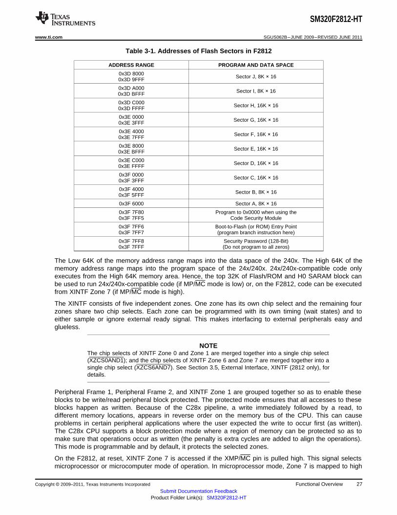
Table 3-1. Addresses of Flash Sectors in F2812
ADDRESS RANGE PROGRAM AND DATA SPACE
0x3D 8000 Sector J, 8K × 160x3D 9FFF
0x3D A000 Sector I, 8K × 160x3D BFFF
0x3D C000 Sector H, 16K × 160x3D FFFF
0x3E 0000 Sector G, 16K × 160x3E 3FFF
0x3E 4000 Sector F, 16K × 160x3E 7FFF
0x3E 8000 Sector E, 16K × 160x3E BFFF
0x3E C000 Sector D, 16K × 160x3E FFFF
0x3F 0000 Sector C, 16K × 160x3F 3FFF
0x3F 4000 Sector B, 8K × 160x3F 5FFF
0x3F 6000 Sector A, 8K × 16
0x3F 7F80 Program to 0x0000 when using the0x3F 7FF5 Code Security Module
0x3F 7FF6 Boot-to-Flash (or ROM) Entry Point0x3F 7FF7 (program branch instruction here)
0x3F 7FF8 Security Password (128-Bit)0x3F 7FFF (Do not program to all zeros)
The Low 64K of the memory address range maps into the data space of the 240x. The High 64K of thememory address range maps into the program space of the 24x/240x. 24x/240x-compatible code onlyexecutes from the High 64K memory area. Hence, the top 32K of Flash/ROM and H0 SARAM block canbe used to run 24x/240x-compatible code (if MP/MC mode is low) or, on the F2812, code can be executedfrom XINTF Zone 7 (if MP/MC mode is high).
The XINTF consists of five independent zones. One zone has its own chip select and the remaining fourzones share two chip selects. Each zone can be programmed with its own timing (wait states) and toeither sample or ignore external ready signal. This makes interfacing to external peripherals easy andglueless.
NOTEThe chip selects of XINTF Zone 0 and Zone 1 are merged together into a single chip select(XZCS0AND1); and the chip selects of XINTF Zone 6 and Zone 7 are merged together into asingle chip select (XZCS6AND7). See Section 3.5, External Interface, XINTF (2812 only), fordetails.
Peripheral Frame 1, Peripheral Frame 2, and XINTF Zone 1 are grouped together so as to enable theseblocks to be write/read peripheral block protected. The protected mode ensures that all accesses to theseblocks happen as written. Because of the C28x pipeline, a write immediately followed by a read, todifferent memory locations, appears in reverse order on the memory bus of the CPU. This can causeproblems in certain peripheral applications where the user expected the write to occur first (as written).The C28x CPU supports a block protection mode where a region of memory can be protected so as tomake sure that operations occur as written (the penalty is extra cycles are added to align the operations).This mode is programmable and by default, it protects the selected zones.
On the F2812, at reset, XINTF Zone 7 is accessed if the XMP/MC pin is pulled high. This signal selectsmicroprocessor or microcomputer mode of operation. In microprocessor mode, Zone 7 is mapped to high
Copyright © 2009–2011, Texas Instruments Incorporated Functional Overview 27Submit Documentation Feedback
Product Folder Link(s): SM320F2812-HT

SM320F2812-HT
SGUS062B–JUNE 2009–REVISED JUNE 2011 www.ti.com
memory such that the vector table is fetched externally. The Boot ROM is disabled in this mode. Inmicrocomputer mode, Zone 7 is disabled such that the vectors are fetched from Boot ROM. This allowsthe user to either boot from on-chip memory or from off-chip memory. The state of the XMP/MC signal onreset is stored in an MP/MC mode bit in the XINTCNF2 register. The user can change this mode insoftware and hence control the mapping of Boot ROM and XINTF Zone 7. No other memory blocks areaffected by XMP/MC.
I/O space is not supported on the F2812 XINTF.
The wait states for the various spaces in the memory map area are listed in Table 3-2.
Table 3-2. Wait States
AREA WAIT-STATES COMMENTS
M0 and M1 SARAMs 0-wait Fixed
Peripheral Frame 0 0-wait Fixed
0-wait (writes)Peripheral Frame 1 Fixed2-wait (reads)
0-wait (writes)Peripheral Frame 2 Fixed2-wait (reads)
L0 and L1 SARAMs 0-wait
Programmable, Programmed via the Flash registers. 1-wait-state operation is possible at a reducedOTP (or ROM) 1-wait minimum CPU frequency. See Section 3.2.6, Flash (F281x Only), for more information.
Programmed via the Flash registers. 0-wait-state operation is possible at reducedProgrammable,Flash (or ROM) CPU frequency. The CSM password locations are hardwired for 16 wait-states.0-wait minimum See Section 3.2.6, Flash (F281x Only), for more information.
H0 SARAM 0-wait Fixed
Boot-ROM 1-wait Fixed
Programmed via the XINTF registers.Programmable,XINTF Cycles can be extended by external memory or peripheral.1-wait minimum 0-wait operation is not possible.
28 Functional Overview Copyright © 2009–2011, Texas Instruments Incorporated
Submit Documentation FeedbackProduct Folder Link(s): SM320F2812-HT
SM320F2812-HT
www.ti.com SGUS062B–JUNE 2009–REVISED JUNE 2011
3.2 Brief Descriptions
3.2.1 C28x CPU
The C28x™ DSP generation is the newest member of the TMS320C2000™ DSP platform. The C28x issource code compatible to the 24x/240x DSP devices, hence existing 240x users can leverage theirsignificant software investment. Additionally, the C28x is a very efficient C/C++ engine, hence enablingusers to develop not only their system control software in a high-level language, but also enables mathalgorithms to be developed using C/C++. The C28x is as efficient in DSP math tasks as it is in systemcontrol tasks that typically are handled by microcontroller devices. This efficiency removes the need for asecond processor in many systems. The 32 × 32-bit MAC capabilities of the C28x and its 64-bitprocessing capabilities, enable the C28x to efficiently handle higher numerical resolution problems thatwould otherwise demand a more expensive floating-point processor solution. Add to this the fast interruptresponse with automatic context save of critical registers, resulting in a device that is capable of servicingmany asynchronous events with minimal latency. The C28x has an 8-level-deep protected pipeline withpipelined memory accesses. This pipelining enables the C28x to execute at high speeds without resortingto expensive high-speed memories. Special branch-look-ahead hardware minimizes the latency forconditional discontinuities. Special store conditional operations further improve performance.
3.2.2 Memory Bus (Harvard Bus Architecture)
As with many DSP type devices, multiple busses are used to move data between the memories andperipherals and the CPU. The C28x memory bus architecture contains a program read bus, data read busand data write bus. The program read bus consists of 22 address lines and 32 data lines. The data readand write busses consist of 32 address lines and 32 data lines each. The 32-bit-wide data busses enablesingle cycle 32-bit operations. The multiple bus architecture, commonly termed Harvard Bus, enables theC28x to fetch an instruction, read a data value and write a data value in a single cycle. All peripherals andmemories attached to the memory bus prioritizes memory accesses. Generally, the priority of Memory Busaccesses can be summarized as follows:
Highest: Data Writes (1)
Program Writes
Data Reads
Program Reads (2)
Lowest: Fetches
3.2.3 Peripheral Bus
To enable migration of peripherals between various Texas Instruments (TI) DSP families, the F2812adopts a peripheral bus standard for peripheral interconnect. The peripheral bus bridge multiplexes thevarious busses that make up the processor Memory Bus into a single bus consisting of 16 address linesand 16 or 32 data lines and associated control signals. Two versions of the peripheral bus are supportedon the F2812. One version only supports 16-bit accesses (called peripheral frame 2) and this retainscompatibility with C240x-compatible peripherals. The other version supports both 16- and 32-bit accesses(called peripheral frame 1).
3.2.4 Real-Time JTAG and Analysis
The F2812 implement the standard IEEE 1149.1 JTAG interface. Additionally, the F2812 supportsreal-time mode of operation whereby the contents of memory, peripheral and register locations can bemodified while the processor is running and executing code and servicing interrupts. The user can also
(1) Simultaneous Data and Program writes cannot occur on the Memory Bus.(2) Simultaneous Program Reads and Fetches cannot occur on the Memory Bus.
Copyright © 2009–2011, Texas Instruments Incorporated Functional Overview 29Submit Documentation Feedback
Product Folder Link(s): SM320F2812-HT

SM320F2812-HT
SGUS062B–JUNE 2009–REVISED JUNE 2011 www.ti.com
single step through non-time critical code while enabling time-critical interrupts to be serviced withoutinterference. The F2812 implements the real-time mode in hardware within the CPU. This is a uniquefeature to the F2812, no software monitor is required. Additionally, special analysis hardware is providedwhich allows the user to set hardware breakpoint or data/address watch-points and generate various userselectable break events when a match occurs.
3.2.5 External Interface (XINTF)
This asynchronous interface consists of 19 address lines, 16 data lines, and three chip-select lines. Thechip-select lines are mapped to five external zones, Zones 0, 1, 2, 6, and 7. Zones 0 and 1 share a singlechip-select; Zones 6 and 7 also share a single chip-select. Each of the five zones can be programmedwith a different number of wait states, strobe signal setup and hold timing and each zone can beprogrammed for extending wait states externally or not. The programmable wait-state, chip-select, andprogrammable strobe timing enables glueless interface to external memories and peripherals.
3.2.6 Flash
The F2812 contains 128K × 16 of embedded flash memory, segregated into four 8K × 16 sectors, and six16K × 16 sectors. The F2810 has 64K × 16 of embedded flash, segregated into two 8K × 16 sectors, andthree 16K × 16 sectors. The device also contains a single 1K × 16 of OTP memory at address range 0x3D7800 - 0x3D 7BFF. The user can individually erase, program, and validate a flash sector while leavingother sectors untouched. However, it is not possible to use one sector of the flash or the OTP to executeflash algorithms that erase/program other sectors. Special memory pipelining is provided to enable theflash module to achieve higher performance. The flash/OTP is mapped to both program and data space;therefore, it can be used to execute code or store data information.
NOTEThe F2812 Flash and OTP wait states can be configured by the application. This allowsapplications running at slower frequencies to configure the flash to use fewer wait states.
Flash effective performance can be improved by enabling the flash pipeline mode in theFlash options register. With this mode enabled, effective performance of linear codeexecution is much faster than the raw performance indicated by the wait state configurationalone. The exact performance gain when using the Flash pipeline mode isapplication-dependent. The pipeline mode is not available for the OTP block.
For more information on the Flash options, Flash wait-state, and OTP wait-state registers,see the TMS320x281x System Control and Interrupts Reference Guide (SPRU078).
3.2.7 L0, L1, H0 SARAMs
The F2812 contains an additional 16K × 16 of single-access RAM, divided into three blocks (4K + 4K +8K). Each block can be independently accessed hence minimizing pipeline stalls. Each block is mapped toboth program and data space.
3.2.8 Boot ROM
The Boot ROM is factory-programmed with boot-loading software. The Boot ROM program executes afterdevice reset and checks several GPIO pins to determine which boot mode to enter. For example, the usercan select to execute code already present in the internal Flash or download new software to internalRAM through one of several serial ports. Other boot modes exist as well. The Boot ROM also containsstandard tables, such as SIN/COS waveforms, for use in math-related algorithms. Table 3-3 shows thedetails of how various boot modes may be invoked. See the TMS320x281x DSP Boot ROM ReferenceGuide (SPRS095), for more information.
30 Functional Overview Copyright © 2009–2011, Texas Instruments Incorporated
Submit Documentation FeedbackProduct Folder Link(s): SM320F2812-HT

SM320F2812-HT
www.ti.com SGUS062B–JUNE 2009–REVISED JUNE 2011
Table 3-3. Boot Mode Selection
GPIOF4 GPIOF12 GPIOF3 GPIOF2BOOT MODE SELECTED (1)(SCITXDA) (MDXA) (SPISTEA) (SPICLK) (2)
GPIO PU status (3) PU No PU No PU No PU
Jump to Flash/ROM address 0x3F 7FF6A branch instruction must have been programmed here prior to 1 x x xreset to redirect code execution as desired.
Call SPI_Boot to load from an external serial SPI EEPROM 0 1 x x
Call SCI_Boot to load from SCI-A 0 0 1 1
Jump to H0 SARAM address 0x3F 8000 0 0 1 0
Jump to OTP address 0x3D 7800 0 0 0 1
Call Parallel_Boot to load from GPIO Port B 0 0 0 0
(1) If the boot mode selected is Flash, H0, or OTP, then no external code is loaded by the bootloader.(2) Extra care must be taken due to any effect toggling SPICLK to select a boot mode may have on external logic.(3) PU = pin has an internal pullup. No PU = pin does not have an internal pullup
3.2.9 Security
The F2812 supports high levels of security to protect the user firmware from being reversed engineered.The security features a 128–bit password (hardcoded for 16 wait states), which the user programs into theflash. One code security module (CSM) is used to protect the flash/ROM/OTP and the L0/L1 SARAMblocks. The security feature prevents unauthorized users from examining the memory contents via theJTAG port, executing code from external memory or trying to boot–load some undesirable software thatwould export the secure memory contents. To enable access to the secure blocks, the user must write thecorrect 128–bit KEY value, which matches the value stored in the password locations within theFlash/ROM.
NOTEFor code security operation, all addresses between 0x3F7F80 and 0x3F7FF5 cannot beused as program code or data, but must be programmed to 0x0000 when the Code SecurityPasswords are programmed. If security is not a concern, then these addresses may be usedfor code or data.
The 128-bit password (at 0x3F 7FF8 – 0x3F 7FFF) must not be programmed to zeros. Doingso would permanently lock the device.
Code Security Module Disclaimer
The Code Security Module (CSM) included on this device was designed to passwordprotect the data stored in the associated memory (either ROM or Flash) and is warrantedby Texas Instruments (TI), in accordance with its standard terms and conditions, toconform to TI’s published specifications for the warranty period applicable for this device.
TI DOES NOT, HOWEVER, WARRANT OR REPRESENT THAT THE CSM CANNOTBE COMPROMISED OR BREACHED OR THAT THE DATA STORED IN THEASSOCIATED MEMORY CANNOT BE ACCESSED THROUGH OTHER MEANS.MOREOVER, EXCEPT AS SET FORTH ABOVE, TI MAKES NO WARRANTIES ORREPRESENTATIONS CONCERNING THE CSM OR OPERATION OF THIS DEVICE,INCLUDING ANY IMPLIED WARRANTIES OF MERCHANTABILITY OR FITNESS FORA PARTICULAR PURPOSE.
Copyright © 2009–2011, Texas Instruments Incorporated Functional Overview 31Submit Documentation Feedback
Product Folder Link(s): SM320F2812-HT

SM320F2812-HT
SGUS062B–JUNE 2009–REVISED JUNE 2011 www.ti.com
IN NO EVENT SHALL TI BE LIABLE FOR ANY CONSEQUENTIAL, SPECIAL,INDIRECT, INCIDENTAL, OR PUNITIVE DAMAGES, HOWEVER CAUSED, ARISINGIN ANY WAY OUT OF YOUR USE OF THE CSM OR THIS DEVICE, WHETHER ORNOT TI HAS BEEN ADVISED OF THE POSSIBILITY OF SUCH DAMAGES.EXCLUDED DAMAGES INCLUDE, BUT ARE NOT LIMITED TO LOSS OF DATA, LOSSOF GOODWILL, LOSS OF USE OR INTERRUPTION OF BUSINESS OR OTHERECONOMIC LOSS.
3.2.10 Peripheral Interrupt Expansion (PIE) Block
The PIE block serves to multiplex numerous interrupt sources into a smaller set of interrupt inputs. ThePIE block can support up to 96 peripheral interrupts. On the F2812, 45 of the possible 96 interrupts areused by peripherals. The 96 interrupts are grouped into blocks of 8 and each group is fed into 1 of 12CPU interrupt lines (INT1 to INT12). Each of the 96 interrupts is, supported by its own vector stored in adedicated RAM block that can be overwritten by the user. The vector is, automatically fetched by the CPUon servicing the interrupt. It takes 8 CPU clock cycles to fetch the vector and save critical CPU registers.Hence the CPU can quickly respond to interrupt events. Prioritization of interrupts is controlled inhardware and software. Each individual interrupt can be enabled/disabled within the PIE block.
3.2.11 External Interrupts (XINT1, XINT2, XINT13, XNMI)
The F2812 supports three masked external interrupts (XINT1, 2, 13). XINT13 is combined with onenon-masked external interrupt (XNMI). The combined signal name is XNMI_XINT13. Each of the interruptscan be selected for negative or positive edge triggering and can also be enabled/disabled (including theXNMI). The masked interrupts also contain a 16-bit free running up counter, which is reset to zero when avalid interrupt edge is detected. This counter can be used to accurately time stamp the interrupt.
3.2.12 Oscillator and PLL
The F2812 can be clocked by an external oscillator or by a crystal attached to the on-chip oscillator circuit.A PLL is provided supporting up to 10-input clock-scaling ratios. The PLL ratios can be changed on-the-flyin software, enabling the user to scale back on operating frequency if lower power operation is desired.Refer to the Electrical Specification section for timing details. The PLL block can be set in bypass mode.
3.2.13 Watchdog
The F2812 supports a watchdog timer. The user software must regularly reset the watchdog counterwithin a certain time frame; otherwise, the watchdog generates a reset to the processor. The watchdogcan be disabled if necessary.
3.2.14 Peripheral Clocking
The clocks to each individual peripheral can be enabled/disabled so as to reduce power consumptionwhen a peripheral is not in use. Additionally, the system clock to the serial ports (except eCAN) and theevent managers, CAP and QEP blocks can be scaled relative to the CPU clock. This enables the timing ofperipherals to be decoupled from increasing CPU clock speeds.
3.2.15 Low-Power Modes
The F2812 device is a full-static CMOS device. Three low-power modes are provided:
IDLE: Place CPU into low-power mode. Peripheral clocks may be turned off selectivelyand only those peripherals that need to function during IDLE are left operating. Anenabled interrupt from an active peripheral wakes the processor from IDLE mode.
STANDBY: Turn off clock to CPU and peripherals. This mode leaves the oscillator and PLLfunctional. An external interrupt event wakes the processor and the peripherals.Execution begins on the next valid cycle after detection of the interrupt event.
32 Functional Overview Copyright © 2009–2011, Texas Instruments Incorporated
Submit Documentation FeedbackProduct Folder Link(s): SM320F2812-HT

SM320F2812-HT
www.ti.com SGUS062B–JUNE 2009–REVISED JUNE 2011
HALT: Turn off oscillator. This mode basically shuts down the device and places it in thelowest possible power consumption mode. Only a reset or XNMI wakes thedevice from this mode.
3.2.16 Peripheral Frames 0, 1, 2 (PFn)
The F2812 segregates peripherals into three sections. The mapping of peripherals is as follows:
PF0: XINTF: External Interface Configuration Registers (2812 only)
PIE: PIE Interrupt Enable and Control Registers Plus PIE Vector Table
Flash: Flash Control, Programming, Erase, Verify Registers
Timers: CPU-Timers 0, 1, 2 Registers
CSM: Code Security Module KEY Registers
PF1: eCAN: eCAN Mailbox and Control Registers
PF2: SYS: System Control Registers
GPIO: GPIO Mux Configuration and Control Registers
EV: Event Manager (EVA/EVB) Control Registers
McBSP: McBSP Control and TX/RX Registers
SCI: Serial Communications Interface (SCI) Control and RX/TX Registers
SPI: Serial Peripheral Interface (SPI) Control and RX/TX Registers
ADC: 12-Bit ADC Registers
3.2.17 General-Purpose Input/Output (GPIO) Multiplexer
Most of the peripheral signals are multiplexed with general-purpose I/O (GPIO) signals. This enables theuser to use a pin as GPIO if the peripheral signal or function is not used. On reset, all GPIO pins areconfigured as inputs. The user can then individually program each pin for GPIO mode or Peripheral Signalmode. For specific inputs, the user can also select the number of input qualification cycles. This is to filterunwanted noise glitches.
3.2.18 32-Bit CPU Timers (0, 1, 2)
CPU Timers 0, 1, and 2 are identical 32-bit timers with presettable periods and with 16-bit clockprescaling. The timers have a 32-bit count down register, which generates an interrupt when the counterreaches zero. The counter is decremented at the CPU clock speed divided by the prescale value setting.When the counter reaches zero, it is automatically reloaded with a 32-bit period value. CPU Timer 2 isreserved for Real-Time OS (RTOS)/BIOS applications. CPU Timer 1 is also reserved for TI systemfunctions. CPU Timer 2 is connected to INT14 of the CPU. CPU Timer 1 can be connected to INT13 of theCPU. CPU Timer 0 is for general use and is connected to the PIE block.
3.2.19 Control Peripherals
The F2812 supports the following peripherals which are used for embedded control and communication:
EV: The event manager module includes general-purpose timers, full-compare/PWM units,capture inputs (CAP) and quadrature-encoder pulse (QEP) circuits. Two such eventmanagers are provided which enable two three-phase motors to be driven or fourtwo-phase motors. The event managers on the F2812 is compatible to the eventmanagers on the 240x devices (with some minor enhancements).
ADC: The ADC block is a 12-bit converter, single ended, 16-channels. It contains twosample-and-hold units for simultaneous sampling.
Copyright © 2009–2011, Texas Instruments Incorporated Functional Overview 33Submit Documentation Feedback
Product Folder Link(s): SM320F2812-HT

SM320F2812-HT
SGUS062B–JUNE 2009–REVISED JUNE 2011 www.ti.com
3.2.20 Serial Port Peripherals
The F2812 supports the following serial communication peripherals:
eCAN: This is the enhanced version of the CAN peripheral. It supports 32 mailboxes, timestamping of messages, and is CAN 2.0B-compliant.
McBSP: This is the multichannel buffered serial port that is used to connect to E1/T1 lines,phone-quality codecs for modem applications or high-quality stereo-quality Audio DACdevices. The McBSP receive and transmit registers are supported by a 16-level FIFO.This significantly reduces the overhead for servicing this peripheral.
SPI: The SPI is a high-speed, synchronous serial I/O port that allows a serial bit stream ofprogrammed length (one to sixteen bits) to be shifted into and out of the device at aprogrammable bit-transfer rate. Normally, the SPI is used for communications betweenthe DSP controller and external peripherals or another processor. Typical applicationsinclude external I/O or peripheral expansion through devices such as shift registers,display drivers, and ADCs. Multi-device communications are supported by themaster/slave operation of the SPI. On the F2812, the port supports a 16-level receiveand transmit FIFO for reducing servicing overhead.
SCI: The serial communications interface is a two-wire asynchronous serial port, commonlyknown as UART. On the F2812, the port supports a 16-level receive and transmit FIFOfor reducing servicing overhead.
3.3 Register Map
The F2812 device contains three peripheral register spaces. The spaces are categorized as follows:• Peripheral Frame 0: These are peripherals that are mapped directly to the CPU memory bus.
See Table 3-4.• Peripheral Frame 1: These are peripherals that are mapped to the 32-bit peripheral bus.
See Table 3-5.• Peripheral Frame 2: These are peripherals that are mapped to the 16-bit peripheral bus.
See Table 3-6.
34 Functional Overview Copyright © 2009–2011, Texas Instruments Incorporated
Submit Documentation FeedbackProduct Folder Link(s): SM320F2812-HT
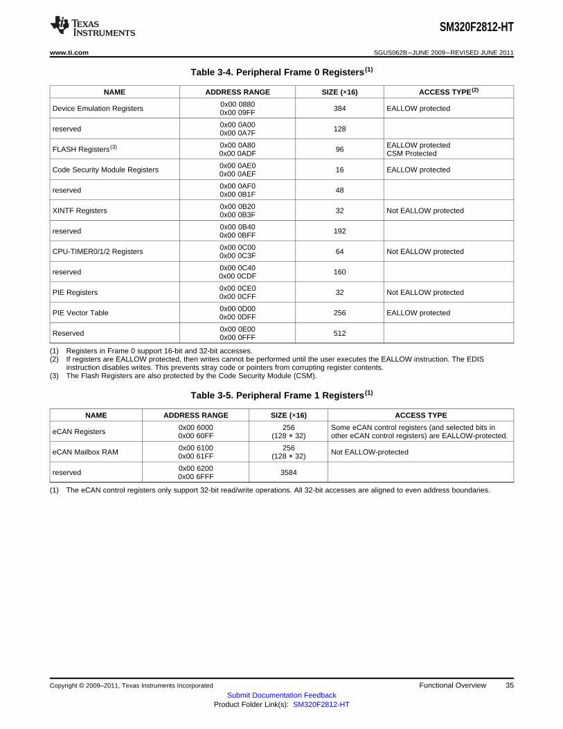
SM320F2812-HT
www.ti.com SGUS062B–JUNE 2009–REVISED JUNE 2011
Table 3-4. Peripheral Frame 0 Registers (1)
NAME ADDRESS RANGE SIZE (×16) ACCESS TYPE (2)
0x00 0880Device Emulation Registers 384 EALLOW protected0x00 09FF
0x00 0A00reserved 1280x00 0A7F
0x00 0A80 EALLOW protectedFLASH Registers (3) 960x00 0ADF CSM Protected
0x00 0AE0Code Security Module Registers 16 EALLOW protected0x00 0AEF
0x00 0AF0reserved 480x00 0B1F
0x00 0B20XINTF Registers 32 Not EALLOW protected0x00 0B3F
0x00 0B40reserved 1920x00 0BFF
0x00 0C00CPU-TIMER0/1/2 Registers 64 Not EALLOW protected0x00 0C3F
0x00 0C40reserved 1600x00 0CDF
0x00 0CE0PIE Registers 32 Not EALLOW protected0x00 0CFF
0x00 0D00PIE Vector Table 256 EALLOW protected0x00 0DFF
0x00 0E00Reserved 5120x00 0FFF
(1) Registers in Frame 0 support 16-bit and 32-bit accesses.(2) If registers are EALLOW protected, then writes cannot be performed until the user executes the EALLOW instruction. The EDIS
instruction disables writes. This prevents stray code or pointers from corrupting register contents.(3) The Flash Registers are also protected by the Code Security Module (CSM).
Table 3-5. Peripheral Frame 1 Registers (1)
NAME ADDRESS RANGE SIZE (×16) ACCESS TYPE
0x00 6000 256 Some eCAN control registers (and selected bits ineCAN Registers 0x00 60FF (128 × 32) other eCAN control registers) are EALLOW-protected.
0x00 6100 256eCAN Mailbox RAM Not EALLOW-protected0x00 61FF (128 × 32)
0x00 6200reserved 35840x00 6FFF
(1) The eCAN control registers only support 32-bit read/write operations. All 32-bit accesses are aligned to even address boundaries.
Copyright © 2009–2011, Texas Instruments Incorporated Functional Overview 35Submit Documentation Feedback
Product Folder Link(s): SM320F2812-HT

SM320F2812-HT
SGUS062B–JUNE 2009–REVISED JUNE 2011 www.ti.com
Table 3-6. Peripheral Frame 2 Registers (1)
NAME ADDRESS RANGE SIZE (×16) ACCESS TYPE
0x00 7000reserved 160x00 700F
0x00 7010System Control Registers 32 EALLOW Protected0x00 702F
0x00 7030reserved 160x00 703F
0x00 7040SPI-A Registers 16 Not EALLOW Protected0x00 704F
0x00 7050SCI-A Registers 16 Not EALLOW Protected0x00 705F
0x00 7060reserved 160x00 706F
0x00 7070External Interrupt Registers 16 Not EALLOW Protected0x00 707F
0x00 7080reserved 640x00 70BF
0x00 70C0GPIO Mux Registers 32 EALLOW Protected0x00 70DF
0x00 70E0GPIO Data Registers 32 Not EALLOW Protected0x00 70FF
0x00 7100ADC Registers 32 Not EALLOW Protected0x00 711F
0x00 7120reserved 7360x00 73FF
0x00 7400EV-A Registers 64 Not EALLOW Protected0x00 743F
0x00 7440reserved 1920x00 74FF
0x00 7500EV-B Registers 64 Not EALLOW Protected0x00 753F
0x00 7540reserved 5280x00 774F
0x00 7750SCI-B Registers 16 Not EALLOW Protected0x00 775F
0x00 7760reserved 1600x00 77FF
0x00 7800McBSP Registers 64 Not EALLOW Protected0x00 783F
0x00 7840reserved 19840x00 7FFF
(1) Peripheral Frame 2 only allows 16-bit accesses. All 32-bit accesses are ignored (invalid data may be returned or written).
36 Functional Overview Copyright © 2009–2011, Texas Instruments Incorporated
Submit Documentation FeedbackProduct Folder Link(s): SM320F2812-HT

SM320F2812-HT
www.ti.com SGUS062B–JUNE 2009–REVISED JUNE 2011
3.4 Device Emulation Registers
These registers are used to control the protection mode of the C28x CPU and to monitor some criticaldevice signals. The registers are defined in Table 3-7.
Table 3-7. Device Emulation Registers
NAME ADDRESS RANGE SIZE (×16) DESCRIPTION
0x00 0880DEVICECNF 2 Device Configuration Register0x00 0881
reserved 0x00 0882 1 Not supported on Revision C and later silicon
Device ID Register (0x0003 – Silicon – Rev. C and D)DEVICEID 0x00 0883 1 Device ID Register (0x0004 – Reserved)
Device ID Register (0x0005 – Silicon – Rev. E)
PROTSTART 0x00 0884 1 Block Protection Start Address Register
PROTRANGE 0x00 0885 1 Block Protection Range Address Register
0x00 0886reserved 3780x00 09FF
3.5 External Interface, XINTF
This section gives a top-level view of the external interface (XINTF) that is implemented on the F2812device.
The external interface is a non-multiplexed asynchronous bus, similar to the C240x external interface. Theexternal interface on the F2812 is mapped into five fixed zones shown in Figure 3-3.
Figure 3-3 shows the F2812 XINTF signals.
Copyright © 2009–2011, Texas Instruments Incorporated Functional Overview 37Submit Documentation Feedback
Product Folder Link(s): SM320F2812-HT

XD(15:0)
XA(18:0)
XZCS6
XZCS7
XZCS6AND7
XZCS2
XWE
XR/WXREADYXMP/MCXHOLD
XHOLDAXCLKOUT
XRD
XINTF Zone 0(8K × 16)
XINTF Zone 1(8K × 16)
XINTF Zone 6(512K × 16)
XINTF Zone 7(16K × 16)
(mapped here if MP/MC = 1)
0x40 0000
0x3F C000
0x18 0000
0x10 0000
0x00 6000
0x00 4000
0x00 2000
0x00 0000
Data Space Prog Space
XINTF Zone 2(512K × 16)
0x08 0000
XZCS0AND1XZCS0XZCS1
SM320F2812-HT
SGUS062B–JUNE 2009–REVISED JUNE 2011 www.ti.com
A. The mapping of XINTF Zone 7 is dependent on the XMP/MC device input signal and the MP/MC mode bit (bit 8 ofXINTCNF2 register). Zones 0, 1, 2, and 6 are always enabled.
B. Each zone can be programmed with different wait states, setup and hold timing, and is supported by zone chipselects (XZCS0AND1, XZCS2, XZCS6AND7), which toggle when an access to a particular zone is performed. Thesefeatures enable glueless connection to many external memories and peripherals.
C. The chip selects for Zone 0 and 1 are ANDed internally together to form one chip select (XZCS0AND1). Any externalmemory that is connected to XZCS0AND1 is dually mapped to both Zones 0 and Zone 1.
D. The chip selects for Zone 6 and 7 are ANDed internally together to form one chip select (XZCS6AND7). Any externalmemory that is connected to XZCS6AND7 is dually mapped to both Zones 6 and Zone 7. This means that if Zone 7 isdisabled (via the MP/MC mode) then any external memory is still accessible via Zone 6 address space.
Figure 3-3. External Interface Block Diagram
38 Functional Overview Copyright © 2009–2011, Texas Instruments Incorporated
Submit Documentation FeedbackProduct Folder Link(s): SM320F2812-HT

SM320F2812-HT
www.ti.com SGUS062B–JUNE 2009–REVISED JUNE 2011
The operation and timing of the external interface, can be controlled by the registers listed in Table 3-8.
Table 3-8. XINTF Configuration and Control Register Mappings
NAME ADDRESS SIZE (×16) DESCRIPTION
XINTF Timing Register, Zone 0 can access as two 16-bit registers or one 32-bitXTIMING0 0x00 0B20 2 register
XINTF Timing Register, Zone 1 can access as two 16-bit registers or one 32-bitXTIMING1 0x00 0B22 2 register
XINTF Timing Register, Zone 2 can access as two 16-bit registers or one 32-bitXTIMING2 0x00 0B24 2 register
XINTF Timing Register, Zone 6 can access as two 16-bit registers or one 32-bitXTIMING6 0x00 0B2C 2 register
XINTF Timing Register, Zone 7 can access as two 16-bit registers or one 32-bitXTIMING7 0x00 0B2E 2 register
XINTF Configuration Register can access as two 16-bit registers or one 32-bitXINTCNF2 0x00 0B34 2 register
XBANK 0x00 0B38 1 XINTF Bank Control Register
XREVISION 0x00 0B3A 1 XINTF Revision Register
3.5.1 Timing Registers
XINTF signal timing can be tuned to match specific external device requirements such as setup and holdtimes to strobe signals for contention avoidance and maximizing bus efficiency. The timing parameterscan be configured individually for each zone. This allows the programmer to maximize the efficiency of thebus, based on the type of memory or peripheral that the user needs to access. All XINTF timing valuesare with respect to XTIMCLK, which is equal to or one-half of the SYSCLKOUT rate, as shown in Figure6-27.
For detailed information on the XINTF timing and configuration register bit fields, see the TMS320x281xDSP External Interface (XINTF) Reference Guide (SPRU067).
3.5.2 XREVISION Register
The XREVISION register contains a unique number to identify the particular version of XINTF used in theproduct. For the F2812, this register is configured as described in Table 3-9.
Table 3-9. XREVISION Register Bit Definitions
BIT(S) NAME TYPE RESET DESCRIPTION
Current XINTF Revision. For internal use/reference. Test purposes only.15-0 REVISION R 0x0004 Subject to change.
Copyright © 2009–2011, Texas Instruments Incorporated Functional Overview 39Submit Documentation Feedback
Product Folder Link(s): SM320F2812-HT

C28x CPU
PIE
TIMER 2 (for RTOS)
TIMER 0
Watchdog
Peripherals (SPI, SCI, McBSP , CAN, EV, ADC)(41 Interrupts)
96 In
terr
upts
†
TINT0
Interrupt Control
XNMICR(15:0)
XINT1Interrupt Control
XINT1CR(15:0)
XINT2Interrupt Control
XINT2CR(15:0)
GPIOMUX
WDINT
INT1 to INT12
INT13
INT14
NMI
XINT1CTR(15:0)
XINT2CTR(15:0)
XNMICTR(15:0)
TIMER 1 (for RTOS)
TINT2
Low-Power ModesLPMINT
WAKEINT
XNMI_XINT13
MU
X
TINT1
enable
select
† Out of a possible 96 interrupts, 45 are currently used by peripherals.
SM320F2812-HT
SGUS062B–JUNE 2009–REVISED JUNE 2011 www.ti.com
3.6 Interrupts
Figure 3-4 shows how the various interrupt sources are multiplexed within the F2812 device.
Figure 3-4. Interrupt Sources
Eight PIE block interrupts are grouped into one CPU interrupt. In total, 12 CPU interrupt groups, with 8interrupts per group equals 96 possible interrupts. On the F2812, 45 of these are used by peripherals asshown in Table 3-10.
40 Functional Overview Copyright © 2009–2011, Texas Instruments Incorporated
Submit Documentation FeedbackProduct Folder Link(s): SM320F2812-HT

INT12
MUX
INT11
INT2INT1
CPU
(Enable)(Flag)
INTx
INTx.8
PIEIERx(8:1) PIEIFRx(8:1)
MUX
INTx.7INTx.6INTx.5INTx.4INTx.3INTx.2INTx.1
FromPeripherals or
ExternalInterrupts
(Enable) (Flag)
IER(12:1)IFR(12:1)
GlobalEnable
INTM
1
0
PIEACKx
(Enable/Flag)
SM320F2812-HT
www.ti.com SGUS062B–JUNE 2009–REVISED JUNE 2011
Figure 3-5. Multiplexing of Interrupts Using the PIE Block
Table 3-10. PIE Peripheral Interrupts (1)
PIE INTERRUPTSCPUINTERRUPTS INTx.8 INTx.7 INTx.6 INTx.5 INTx.4 INTx.3 INTx.2 INTx.1
WAKEINT TINT0 ADCINT PDPINTB PDPINTAINT1 XINT2 XINT1 reserved(LPM/WD) (TIMER 0) (ADC) (EV-B) (EV-A)
T1OFINT T1UFINT T1CINT T1PINT CMP3INT CMP2INT CMP1INTINT2 reserved (EV-A) (EV-A) (EV-A) (EV-A) (EV-A) (EV-A) (EV-A)
CAPINT3 CAPINT2 CAPINT1 T2OFINT T2UFINT T2CINT T2PINTINT3 reserved (EV-A) (EV-A) (EV-A) (EV-A) (EV-A) (EV-A) (EV-A)
T3OFINT T3UFINT T3CINT T3PINT CMP6INT CMP5INT CMP4INTINT4 reserved (EV-B) (EV-B) (EV-B) (EV-B) (EV-B) (EV-B) (EV-B)
CAPINT6 CAPINT5 CAPINT4 T4OFINT T4UFINT T4CINT T4PINTINT5 reserved (EV-B) (EV-B) (EV-B) (EV-B) (EV-B) (EV-B) (EV-B)
MXINT MRINT SPITXINTA SPIRXINTAINT6 reserved reserved reserved reserved(McBSP) (McBSP) (SPI) (SPI)
INT7 reserved reserved reserved reserved reserved reserved reserved reserved
INT8 reserved reserved reserved reserved reserved reserved reserved reserved
ECAN1INT ECAN0INT SCITXINTB SCIRXINTB SCITXINTA SCIRXINTAINT9 reserved reserved (CAN) (CAN) (SCI-B) (SCI-B) (SCI-A) (SCI-A)
INT10 reserved reserved reserved reserved reserved reserved reserved reserved
INT11 reserved reserved reserved reserved reserved reserved reserved reserved
INT12 reserved reserved reserved reserved reserved reserved reserved reserved
(1) Out of the 96 possible interrupts, 45 interrupts are currently used. the remaining interrupts are reserved for future devices. However,these interrupts can be used as software interrupts if they are enabled at the PIEIFRx level.
Copyright © 2009–2011, Texas Instruments Incorporated Functional Overview 41Submit Documentation Feedback
Product Folder Link(s): SM320F2812-HT

SM320F2812-HT
SGUS062B–JUNE 2009–REVISED JUNE 2011 www.ti.com
Table 3-11. PIE Configuration and Control Registers (1)
NAME ADDRESS SIZE (×16) DESCRIPTION
PIECTRL 0x0000-0CE0 1 PIE, Control Register
PIEACK 0x0000-0CE1 1 PIE, Acknowledge Register
PIEIER1 0x0000-0CE2 1 PIE, INT1 Group Enable Register
PIEIFR1 0x0000-0CE3 1 PIE, INT1 Group Flag Register
PIEIER2 0x0000-0CE4 1 PIE, INT2 Group Enable Register
PIEIFR2 0x0000-0CE5 1 PIE, INT2 Group Flag Register
PIEIER3 0x0000-0CE6 1 PIE, INT3 Group Enable Register
PIEIFR3 0x0000-0CE7 1 PIE, INT3 Group Flag Register
PIEIER4 0x0000-0CE8 1 PIE, INT4 Group Enable Register
PIEIFR4 0x0000-0CE9 1 PIE, INT4 Group Flag Register
PIEIER5 0x0000-0CEA 1 PIE, INT5 Group Enable Register
PIEIFR5 0x0000-0CEB 1 PIE, INT5 Group Flag Register
PIEIER6 0x0000-0CEC 1 PIE, INT6 Group Enable Register
PIEIFR6 0x0000-0CED 1 PIE, INT6 Group Flag Register
PIEIER7 0x0000-0CEE 1 PIE, INT7 Group Enable Register
PIEIFR7 0x0000-0CEF 1 PIE, INT7 Group Flag Register
PIEIER8 0x0000-0CF0 1 PIE, INT8 Group Enable Register
PIEIFR8 0x0000-0CF1 1 PIE, INT8 Group Flag Register
PIEIER9 0x0000-0CF2 1 PIE, INT9 Group Enable Register
PIEIFR9 0x0000-0CF3 1 PIE, INT9 Group Flag Register
PIEIER10 0x0000-0CF4 1 PIE, INT10 Group Enable Register
PIEIFR10 0x0000-0CF5 1 PIE, INT10 Group Flag Register
PIEIER11 0x0000-0CF6 1 PIE, INT11 Group Enable Register
PIEIFR11 0x0000-0CF7 1 PIE, INT11 Group Flag Register
PIEIER12 0x0000-0CF8 1 PIE, INT12 Group Enable Register
PIEIFR12 0x0000-0CF9 1 PIE, INT12 Group Flag Register
0x0000-0CFAReserved 6 Reserved0x0000-0CFF
(1) The PIE configuration and control registers are not protected by EALLOW mode. The PIE vector table is protected.
42 Functional Overview Copyright © 2009–2011, Texas Instruments Incorporated
Submit Documentation FeedbackProduct Folder Link(s): SM320F2812-HT
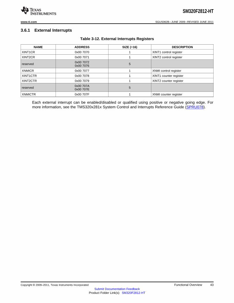
SM320F2812-HT
www.ti.com SGUS062B–JUNE 2009–REVISED JUNE 2011
3.6.1 External Interrupts
Table 3-12. External Interrupts Registers
NAME ADDRESS SIZE (×16) DESCRIPTION
XINT1CR 0x00 7070 1 XINT1 control register
XINT2CR 0x00 7071 1 XINT2 control register
0x00 7072reserved 50x00 7076
XNMICR 0x00 7077 1 XNMI control register
XINT1CTR 0x00 7078 1 XINT1 counter register
XINT2CTR 0x00 7079 1 XINT2 counter register
0x00 707Areserved 50x00 707E
XNMICTR 0x00 707F 1 XNMI counter register
Each external interrupt can be enabled/disabled or qualified using positive or negative going edge. Formore information, see the TMS320x281x System Control and Interrupts Reference Guide (SPRU078).
Copyright © 2009–2011, Texas Instruments Incorporated Functional Overview 43Submit Documentation Feedback
Product Folder Link(s): SM320F2812-HT

See Note A
SM320F2812-HT
SGUS062B–JUNE 2009–REVISED JUNE 2011 www.ti.com
3.7 System Control
This section describes the F2812 oscillator, PLL and clocking mechanisms, the watchdog function and thelow power modes. Figure 3-6 shows the various clock and reset domains in the F2812 device that arediscussed.
A. CLKIN is the clock input to the CPU. SYSCLKOUT is the output clock of the CPU. They are of the same frequency.
Figure 3-6. Clock and Reset Domains
44 Functional Overview Copyright © 2009–2011, Texas Instruments Incorporated
Submit Documentation FeedbackProduct Folder Link(s): SM320F2812-HT

SM320F2812-HT
www.ti.com SGUS062B–JUNE 2009–REVISED JUNE 2011
The PLL, clocking, watchdog, and low-power modes are controlled by the registers listed in Table 3-13.
Table 3-13. PLL, Clocking, Watchdog, and Low-Power Mode Registers (1)
NAME ADDRESS SIZE (×16) DESCRIPTION
0x00 7010reserved 80x00 7017
reserved 0x00 7018 1
reserved 0x00 7019 1
HISPCP 0x00 701A 1 High-Speed Peripheral Clock Prescaler Register for HSPCLK clock
LOSPCP 0x00 701B 1 Low-Speed Peripheral Clock Prescaler Register for LSPCLK clock
PCLKCR 0x00 701C 1 Peripheral Clock Control Register
reserved 0x00 701D 1
LPMCR0 0x00 701E 1 Low Power Mode Control Register 0
LPMCR1 0x00 701F 1 Low Power Mode Control Register 1
reserved 0x00 7020 1
PLLCR 0x00 7021 1 PLL Control Register (2)
SCSR 0x00 7022 1 System Control & Status Register
WDCNTR 0x00 7023 1 Watchdog Counter Register
reserved 0x00 7024 1
WDKEY 0x00 7025 1 Watchdog Reset Key Register
0x00 7026reserved 30x00 7028
WDCR 0x00 7029 1 Watchdog Control Register
0x00 702Areserved 60x00 702F
(1) All of the above registers can only be accessed by executing the EALLOW instruction.(2) The PLL control register (PLLCR) is reset to a known state by the XRS signal only. Emulation reset (through Code Composer Studio)
does not reset PLLCR.
Copyright © 2009–2011, Texas Instruments Incorporated Functional Overview 45Submit Documentation Feedback
Product Folder Link(s): SM320F2812-HT

X2
X1/XCLKIN
On-ChipOscillator
(OSC)PLL
Bypass /2
XF_XPLLDIS
OSCCLK (PLL Disabled)
LatchXPLLDIS
XRS
PLL
4-Bit PLL Select
SYSCLKOUT
1
0
CLKINCPU
4-Bit PLL Select
XCLKIN
PLL Block
SM320F2812-HT
SGUS062B–JUNE 2009–REVISED JUNE 2011 www.ti.com
3.8 OSC and PLL Block
Figure 3-7 shows the OSC and PLL block on the F2812.
Figure 3-7. OSC and PLL Block
The on-chip oscillator circuit enables a crystal to be attached to the F2812 device using the X1/XCLKINand X2 pins. If a crystal is not used, then an external oscillator can be directly connected to theX1/XCLKIN pin and the X2 pin is left unconnected. The logic-high level in this case should not exceedVDD. The PLLCR bits [3:0] set the clocking ratio.
Table 3-14. PLLCR Register Bit Definitions
BIT(S) NAME TYPE XRS RESET (1) DESCRIPTION
15:04 reserved R = 0 0:00
SYSCLKOUT = (XCLKIN x n)/2, where n is the PLL multiplication factor.
Bit Value n SYSCLKOUT
0000 PLL Bypassed XCLKIN/20001 1 XCLKIN/20010 2 XCLKIN0011 3 XCLKIN × 1.50100 4 XCLKIN × 20101 5 XCLKIN × 2.50110 6 XCLKIN × 33:00 DIV R/W 0,0,0,00111 7 XCLKIN × 3.51000 8 XCLKIN × 41001 9 XCLKIN × 4.51010 10 XCLKIN × 51011 11 Reserved1100 12 Reserved1101 13 Reserved1110 14 Reserved1111 15 Reserved
(1) The PLLCR register is reset to a known state by the XRS reset line. If a reset is issued by the debugger, the PLL clocking ratio is notchanged.
46 Functional Overview Copyright © 2009–2011, Texas Instruments Incorporated
Submit Documentation FeedbackProduct Folder Link(s): SM320F2812-HT

External Clock Signal (Toggling 0 −VDD)
Cb1(see Note A)
X2X1/XCLKIN X1/XCLKIN X2
CrystalCb2(see Note A)
(a) (b)
NC
SM320F2812-HT
www.ti.com SGUS062B–JUNE 2009–REVISED JUNE 2011
3.8.1 Loss of Input Clock
In PLL enabled mode, if the input clock XCLKIN or the oscillator clock is removed or absent, the PLL stillissues a limp-mode clock. The limp-mode clock continues to clock the CPU and peripherals at a typicalfrequency of 1 MHz to 4 MHz. The PLLCR register should have been written to with a non-zero value forthis feature to work.
Normally, when the input clocks are present, the watchdog counter decrements to initiate a watchdogreset or WDINT interrupt. However, when the external input clock fails, the watchdog counter stopsdecrementing (i.e., the watchdog counter does not change with the limp-mode clock). This condition couldbe used by the application firmware to detect the input clock failure and initiate necessary shut-downprocedure for the system.
3.9 PLL-Based Clock Module
The F2812 has an on-chip, PLL-based clock module. This module provides all the necessary clockingsignals for the device, as well as control for low-power mode entry. The PLL has a 4-bit ratio control toselect different CPU clock rates. The watchdog module should be disabled before writing to the PLLCRregister. It can be re-enabled (if need be) after the PLL module has stabilized, which takes 131 072XCLKIN cycles.
The PLL-based clock module provides two modes of operation:• Crystal operation
This mode allows the use of an external crystal/resonator to provide the time base to the device.• External clock source operation
This mode allows the internal oscillator to be bypassed. The device clocks are generated from anexternal clock source input on the X1/XCLKIN pin.
A. TI recommends that customers have the resonator/crystal vendor characterize the operation of their device with theDSP chip. The resonator/crystal vendor has the equipment and expertise to tune the tank circuit. The vendor can alsoadvise the customer regarding the proper tank component values that ensures start-up and stability over the entireoperating range.
Figure 3-8. Recommended Crystal/Clock Connection
Table 3-15. Possible PLL Configuration Modes
PLL MODE REMARKS SYSCLKOUT
Invoked by tying XPLLDIS pin low upon reset. PLL block is completely disabled. Clock inputPLL Disabled XCLKINto the CPU (CLKIN) is directly derived from the clock signal present at the X1/XCLKIN pin.
Default PLL configuration upon power-up, if PLL is not disabled. The PLL itself is bypassed.PLL Bypassed However, the /2 module in the PLL block divides the clock input at the X1/XCLKIN pin by XCLKIN/2
two before feeding it to the CPU.
Achieved by writing a non-zero value n into PLLCR register. The /2 module in the PLL blockPLL Enabled (XCLKIN × n) / 2now divides the output of the PLL by two before feeding it to the CPU.
3.10 External Reference Oscillator Clock Option
The typical specifications for the external quartz crystal for a frequency of 30 MHz are listed below:• Fundamental mode, parallel resonant• CL (load capacitance) = 12 pF
Copyright © 2009–2011, Texas Instruments Incorporated Functional Overview 47Submit Documentation Feedback
Product Folder Link(s): SM320F2812-HT

/512OSCCLK
WDCR (WDPS(2:0))
WDCLK
WDCNTR(7:0)
WDKEY(7:0)Bad Key
Good Key
1 0 1
WDCR (WDCHK(2:0))
BadWDCHKKey
WDCR (WDDIS)
Clear Counter
SCSR (WDENINT)
WatchdogPrescaler
GenerateOutput Pulse
(512 OSCCLKs)
8-BitWatchdogCounter
CLR
WDRST
WDINTWatchdog55 + AA
Key DetectorXRS
Core-reset
WDRST(See Note A)
InternalPullup
SM320F2812-HT
SGUS062B–JUNE 2009–REVISED JUNE 2011 www.ti.com
• CL1 = CL2 = 24 pF• Cshunt = 6 pF• ESR range = 25 to 40 Ω
3.11 Watchdog Block
The watchdog block on the F2812 is identical to the one used on the 240x devices. The watchdog modulegenerates an output pulse, 512 oscillator clocks wide (OSCCLK), whenever the 8-bit watchdog up counterhas reached its maximum value. To prevent this, the user disables the counter or the software mustperiodically write a 0x55 + 0xAA sequence into the watchdog key register which resets the watchdogcounter. Figure 3-9 shows the various functional blocks within the watchdog module.
A. The WDRST signal is driven low for 512 OSCCLK cycles.
Figure 3-9. Watchdog Module
The WDINT signal enables the watchdog to be used as a wakeup from IDLE/STANDBY mode timer.
In STANDBY mode, all peripherals are turned off on the device. The only peripheral that remainsfunctional is the watchdog. The WATCHDOG module runs off the PLL clock or the oscillator clock. TheWDINT signal is fed to the LPM block so that it can wake the device from STANDBY (if enabled). SeeSection 3.12, Low-Power Modes Block, for more details.
In IDLE mode, the WDINT signal can generate an interrupt to the CPU, via the PIE, to take the CPU out ofIDLE mode.
In HALT mode, this feature cannot be used because the oscillator (and PLL) are turned off and hence sois the WATCHDOG.
48 Functional Overview Copyright © 2009–2011, Texas Instruments Incorporated
Submit Documentation FeedbackProduct Folder Link(s): SM320F2812-HT

SM320F2812-HT
www.ti.com SGUS062B–JUNE 2009–REVISED JUNE 2011
3.12 Low-Power Modes Block
The low-power modes on the F2812 are similar to the 240x devices. Table 3-16 summarizes the variousmodes.
Table 3-16. F2812 Low-Power Modes
MODE LPM(1:0) OSCCLK CLKIN SYSCLKOUT EXIT (1)
Normal X,X on on on –XRS,
WDINT,IDLE 0,0 on on on (2) Any Enabled Interrupt,
XNMIDebugger (3)
XRS,WDINT,XINT1,XNMI,
on T1/2/3/4CTRIP,STANDBY 0,1 off off(watchdog still running) C1/2/3/4/5/6TRIP,SCIRXDA,SCIRXDB,CANRX,
Debugger (3)
off XRS,HALT 1,X (oscillator and PLL turned off, off off XNMI,
watchdog not functional) Debugger (4)
(1) The Exit column lists which signals or under what conditions the low power mode is exited. A low signal, on any of the signals, exits thelow power condition. This signal must be kept low long enough for an interrupt to be recognized by the device. Otherwise, the IDLEmode is not exited and the device goes back into the indicated low power mode.
(2) The IDLE mode on the C28x behaves differently than on the 24x/240x. On the C28x, the clock output from the core (SYSCLKOUT) isstill functional while on the 24x/240x the clock is turned off.
(3) On the C28x, the JTAG port can still function even if the core clock (CLKIN) is turned off.(4) On the C28x, the JTAG port can still function even if the core clock (CLKIN) is turned off.
The various low-power modes operate as follows:
IDLE Mode: This mode is exited by any enabled interrupt or an XNMI that is recognizedby the processor. The LPM block performs no tasks during this mode as longas the LPMCR0(LPM) bits are set to 0,0.
STANDBY Mode: All other signals (including XNMI) wake the device from STANDBY mode ifselected by the LPMCR1 register. The user needs to select which signal(s)wakes the device. The selected signal(s) are also qualified by the OSCCLKbefore waking the device. The number of OSCCLKs is specified in theLPMCR0 register.
HALT Mode: Only the XRS and XNMI external signals can wake the device from HALTmode. The XNMI input to the core has an enable/disable bit. Hence, it is safeto use the XNMI signal for this function.
NOTEThe low-power modes do not affect the state of the output pins (PWM pins included). Theyare in whatever state the code left them in when the IDLE instruction was executed.
Copyright © 2009–2011, Texas Instruments Incorporated Functional Overview 49Submit Documentation Feedback
Product Folder Link(s): SM320F2812-HT

Borrow
Reset
Timer Reload
SYSCLKOUTTCR.4
(Timer Start Status)
TINT
16-Bit T imer Divide-Down TDDRH:TDDR
32-Bit T imer PeriodPRDH:PRD
32-Bit CounterTIMH:TIM
16-Bit Prescale CounterPSCH:PSC
Borrow
SM320F2812-HT
SGUS062B–JUNE 2009–REVISED JUNE 2011 www.ti.com
4 Peripherals
The integrated peripherals of the F2812 are described in the following subsections:• Three 32-bit CPU-Timers• Two event-manager modules (EVA, EVB)• Enhanced analog-to-digital converter (ADC) module• Enhanced controller area network (eCAN) module• Multichannel buffered serial port (McBSP) module• Serial communications interface modules (SCI-A, SCI-B)• Serial peripheral interface (SPI) module• Digital I/O and shared pin functions
4.1 32-Bit CPU-Timers 0/1/2
There are three 32-bit CPU-timers on the F2812 devices (CPU-TIMER0/1/2).
CPU-Timers 1 and 2 are reserved for the real-time OS (such as DSP/BIOS). CPU-Timer 0 can be used inuser applications. These timers are different from the general-purpose (GP) timers that are present in theEvent Manager modules (EVA, EVB).
NOTEIf the application is not using DSP/BIOS, then CPU-Timers 1 and 2 can be used in theapplication.
Figure 4-1. CPU-Timers
50 Peripherals Copyright © 2009–2011, Texas Instruments Incorporated
Submit Documentation FeedbackProduct Folder Link(s): SM320F2812-HT

INT1to
INT12
INT14
C28x
TINT2
TINT0PIE CPU-TIMER 0
CPU-TIMER 2 (Reserved for TI
system functions)
INT13TINT1 CPU-TIMER 1
(Reserved for TI system functions)
XINT13
SM320F2812-HT
www.ti.com SGUS062B–JUNE 2009–REVISED JUNE 2011
In the F2812 device, the timer interrupt signals (TINT0, TINT1, TINT2) are connected as shown inFigure 4-2.
A. The timer registers are connected to the Memory Bus of the C28x processor.B. The timing of the timers is synchronized to SYSCLKOUT of the processor clock.
Figure 4-2. CPU-Timer Interrupts Signals and Output Signal (See Notes A. and B.)
The general operation of the timer is as follows: The 32-bit counter register TIMH:TIM is loaded with thevalue in the period register PRDH:PRD. The counter register, decrements at the SYSCLKOUT rate of theC28x. When the counter reaches 0, a timer interrupt output signal generates an interrupt pulse. Theregisters listed in Table 4-1 are used to configure the timers. For more information, see the TMS320x281xSystem Control and Interrupts Reference Guide (SPRU078).
Copyright © 2009–2011, Texas Instruments Incorporated Peripherals 51Submit Documentation Feedback
Product Folder Link(s): SM320F2812-HT

SM320F2812-HT
SGUS062B–JUNE 2009–REVISED JUNE 2011 www.ti.com
Table 4-1. CPU-Timers 0, 1, 2 Configuration and Control Registers
NAME ADDRESS SIZE (×16) DESCRIPTION
TIMER0TIM 0x00 0C00 1 CPU-Timer 0, Counter Register
TIMER0TIMH 0x00 0C01 1 CPU-Timer 0, Counter Register High
TIMER0PRD 0x00 0C02 1 CPU-Timer 0, Period Register
TIMER0PRDH 0x00 0C03 1 CPU-Timer 0, Period Register High
TIMER0TCR 0x00 0C04 1 CPU-Timer 0, Control Register
reserved 0x00 0C05 1
TIMER0TPR 0x00 0C06 1 CPU-Timer 0, Prescale Register
TIMER0TPRH 0x00 0C07 1 CPU-Timer 0, Prescale Register High
TIMER1TIM 0x00 0C08 1 CPU-Timer 1, Counter Register
TIMER1TIMH 0x00 0C09 1 CPU-Timer 1, Counter Register High
TIMER1PRD 0x00 0C0A 1 CPU-Timer 1, Period Register
TIMER1PRDH 0x00 0C0B 1 CPU-Timer 1, Period Register High
TIMER1TCR 0x00 0C0C 1 CPU-Timer 1, Control Register
reserved 0x00 0C0D 1
TIMER1TPR 0x00 0C0E 1 CPU-Timer 1, Prescale Register
TIMER1TPRH 0x00 0C0F 1 CPU-Timer 1, Prescale Register High
TIMER2TIM 0x00 0C10 1 CPU-Timer 2, Counter Register
TIMER2TIMH 0x00 0C11 1 CPU-Timer 2, Counter Register High
TIMER2PRD 0x00 0C12 1 CPU-Timer 2, Period Register
TIMER2PRDH 0x00 0C13 1 CPU-Timer 2, Period Register High
TIMER2TCR 0x00 0C14 1 CPU-Timer 2, Control Register
reserved 0x00 0C15 1
TIMER2TPR 0x00 0C16 1 CPU-Timer 2, Prescale Register
TIMER2TPRH 0x00 0C17 1 CPU-Timer 2, Prescale Register High
0x00 0C18reserved 400x00 0C3F
52 Peripherals Copyright © 2009–2011, Texas Instruments Incorporated
Submit Documentation FeedbackProduct Folder Link(s): SM320F2812-HT

SM320F2812-HT
www.ti.com SGUS062B–JUNE 2009–REVISED JUNE 2011
4.2 Event Manager Modules (EVA, EVB)
The event-manager modules include general-purpose (GP) timers, full-compare/PWM units, capture units,and quadrature-encoder pulse (QEP) circuits. EVA and EVB timers, compare units, and capture unitsfunction identically. However, timer/unit names differ for EVA and EVB. Table 4-2 shows the module andsignal names used. Table 4-2 shows the features and functionality available for the event-managermodules and highlights EVA nomenclature.
Event managers A and B have identical peripheral register sets with EVA starting at 7400h and EVBstarting at 7500h. The paragraphs in this section describe the function of GP timers, compare units,capture units, and QEPs using EVA nomenclature. These paragraphs are applicable to EVB with regard tofunction—however, module/signal names would differ. Table 4-3 lists the EVA registers. For moreinformation, see the TMS320x281x DSP Event Manager (EV) Reference Guide (SPRU065).
Table 4-2. Module and Signal Names for EVA and EVB
EVA EVBEVENT MANAGER MODULES
MODULE SIGNAL MODULE SIGNAL
GP Timer 1 T1PWM/T1CMP GP Timer 3 T3PWM/T3CMPGP Timers GP Timer 2 T2PWM/T2CMP GP Timer 4 T4PWM/T4CMP
Compare 1 PWM1/2 Compare 4 PWM7/8Compare Units Compare 2 PWM3/4 Compare 5 PWM9/10
Compare 3 PWM5/6 Compare 6 PWM11/12
Capture 1 CAP1 Capture 4 CAP4Capture Units Capture 2 CAP2 Capture 5 CAP5
Capture 3 CAP3 Capture 6 CAP6
QEP1 QEP3QEP1 QEP3QEP Channels QEP2 QEP4QEP2 QEP4QEPI1 QEPI2
Direction TDIRA Direction TDIRBExternal Clock Inputs External Clock TCLKINA External Clock TCLKINB
C1TRIP C4TRIPExternal Trip Inputs Compare C2TRIP Compare C5TRIP
C3TRIP C6TRIP
T1CTRIP_PDPINTA T3CTRIP_PDPINTB (1)External Trip Inputs (1)
T4CTRIP/EVBSOCT2CTRIP/EVASOC
(1) In the 24x/240x-compatible mode, the T1CTRIP_PDPINTA pin functions as PDPINTA and the T3CTRIP_PDPINTB pin functions asPDPINTB.
Copyright © 2009–2011, Texas Instruments Incorporated Peripherals 53Submit Documentation Feedback
Product Folder Link(s): SM320F2812-HT

SM320F2812-HT
SGUS062B–JUNE 2009–REVISED JUNE 2011 www.ti.com
Table 4-3. EVA Registers (1)
NAME ADDRESS SIZE (×16) DESCRIPTION
GPTCONA 0x00 7400 1 GP Timer Control Register A
T1CNT 0x00 7401 1 GP Timer 1 Counter Register
T1CMPR 0x00 7402 1 GP Timer 1 Compare Register
T1PR 0x00 7403 1 GP Timer 1 Period Register
T1CON 0x00 7404 1 GP Timer 1 Control Register
T2CNT 0x00 7405 1 GP Timer 2 Counter Register
T2CMPR 0x00 7406 1 GP Timer 2 Compare Register
T2PR 0x00 7407 1 GP Timer 2 Period Register
T2CON 0x00 7408 1 GP Timer 2 Control Register
EXTCONA (2) 0x00 7409 1 GP Extension Control Register A
COMCONA 0x00 7411 1 Compare Control Register A
ACTRA 0x00 7413 1 Compare Action Control Register A
DBTCONA 0x00 7415 1 Dead–Band Timer Control Register A
CMPR1 0x00 7417 1 Compare Register 1
CMPR2 0x00 7418 1 Compare Register 2
CMPR3 0x00 7419 1 Compare Register 3
CAPCONA 0x00 7420 1 Capture Control Register A
CAPFIFOA 0x00 7422 1 Capture FIFO Status Register A
CAP1FIFO 0x00 7423 1 Two-Level Deep Capture FIFO Stack 1
CAP2FIFO 0x00 7424 1 Two-Level Deep Capture FIFO Stack 2
CAP3FIFO 0x00 7425 1 Two–Level Deep Capture FIFO Stack 3
CAP1FBOT 0x00 7427 1 Bottom Register Of Capture FIFO Stack 1
CAP2FBOT 0x00 7428 1 Bottom Register Of Capture FIFO Stack 2
CAP3FBOT 0x00 7429 1 Bottom Register Of Capture FIFO Stack 3
EVAIMRA 0x00 742C 1 Interrupt Mask Register A
EVAIMRB 0x00 742D 1 Interrupt Mask Register B
EVAIMRC 0x00 742E 1 Interrupt Mask Register C
EVAIFRA 0x00 742F 1 Interrupt Flag Register A
EVAIFRB 0x00 7430 1 Interrupt Flag Register B
EVAIFRC 0x00 7431 1 Interrupt Flag Register C
(1) The EV-B register set is identical except the address range is from 0x00–7500 to 0x00–753F. The above registers are mapped to Zone2. This space allows only 16-bit accesses. 32-bit accesses produce undefined results.
(2) New register compared to 24x/240x
54 Peripherals Copyright © 2009–2011, Texas Instruments Incorporated
Submit Documentation FeedbackProduct Folder Link(s): SM320F2812-HT
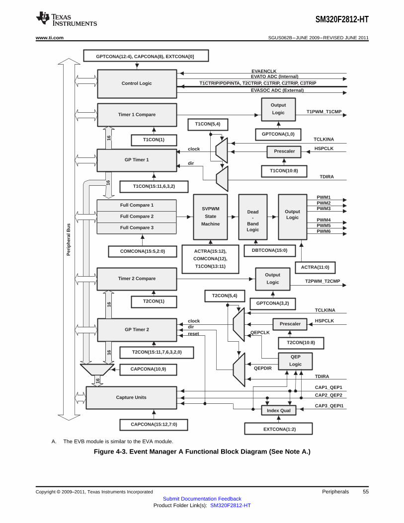
GPTCONA(12:4), CAPCONA(8), EXTCONA[0]
EVATO ADC (Internal)
Timer 1 Compare
Output
Logic T1PWM_T1CMP
GPTCONA(1,0)T1CON(1)
GP Timer 1
TCLKINA
Prescaler HSPCLK
T1CON(10:8)
T1CON(5,4)
clock
Full Compare 1
Full Compare 2
Full Compare 3
SVPWM
State
Machine
Dead-
BandLogic
OutputLogic
PWM1PWM2PWM3
PWM4PWM5PWM6
T1CON(15:11,6,3,2)
TDIRA
dir
Timer 2 Compare
GP Timer 2
16
Capture Units
COMCONA(15:5,2:0)
T1CTRIP/PDPINTA, T2CTRIP, C1TRIP, C2TRIP, C3TRIP
Output
Logic T2PWM_T2CMP
GPTCONA(3,2)T2CON(1)
T2CON(15:11,7,6,3,2,0)
ACTRA(15:12),
COMCONA(12),
T1CON(13:11)
CAPCONA(10,9)
16
DBTCONA(15:0)
ACTRA(11:0)
TCLKINA
PrescalerHSPCLK
T2CON(10:8)
T2CON(5,4)
clockdir
CAPCONA(15:12,7:0)
CAP1_QEP1
CAP2_QEP2
CAP3_QEPI1
QEP
Logic
QEPCLK
QEPDIR
1616
reset
EVAENCLK
Control Logic
Per
iphe
ral B
us
TDIRA
Index Qual
EXTCONA(1:2)
16
EVASOC ADC (External)
SM320F2812-HT
www.ti.com SGUS062B–JUNE 2009–REVISED JUNE 2011
A. The EVB module is similar to the EVA module.
Figure 4-3. Event Manager A Functional Block Diagram (See Note A.)
Copyright © 2009–2011, Texas Instruments Incorporated Peripherals 55Submit Documentation Feedback
Product Folder Link(s): SM320F2812-HT

SM320F2812-HT
SGUS062B–JUNE 2009–REVISED JUNE 2011 www.ti.com
4.2.1 General-Purpose (GP) Timers
There are two GP timers. The GP timer x (x = 1 or 2 for EVA; x = 3 or 4 for EVB) includes:• A 16-bit timer, up-/down-counter, TxCNT, for reads or writes• A 16-bit timer-compare register, TxCMPR (double-buffered with shadow register), for reads or writes• A 16-bit timer-period register, TxPR (double-buffered with shadow register), for reads or writes• A 16-bit timer-control register, TxCON, for reads or writes• Selectable internal or external input clocks• A programmable prescaler for internal or external clock inputs• Control and interrupt logic, for four maskable interrupts: underflow, overflow, timer compare, and period
interrupts• A selectable direction input pin (TDIRx) (to count up or down when directional up- / down-count mode
is selected)
The GP timers can be operated independently or synchronized with each other. The compare registerassociated with each GP timer can be used for compare function and PWM-waveform generation. Thereare three continuous modes of operations for each GP timer in up- or up / down-counting operations.Internal or external input clocks with programmable prescaler are used for each GP timer. GP timers alsoprovide the time base for the other event-manager submodules: GP timer 1 for all the compares and PWMcircuits, GP timer 2/1 for the capture units and the quadrature-pulse counting operations. Double-bufferingof the period and compare registers allows programmable change of the timer (PWM) period and thecompare/PWM pulse width as needed.
4.2.2 Full-Compare Units
There are three full-compare units on each event manager. These compare units use GP timer1 as thetime base and generate six outputs for compare and PWM-waveform generation using programmabledeadband circuit. The state of each of the six outputs is configured independently. The compare registersof the compare units are double-buffered, allowing programmable change of the compare/PWM pulsewidths as needed.
4.2.3 Programmable Deadband Generator
Deadband generation can be enabled/disabled for each compare unit output individually. Thedeadband-generator circuit produces two outputs (with or without deadband zone) for each compare unitoutput signal. The output states of the deadband generator are configurable and changeable as neededby way of the double-buffered ACTRx register.
4.2.4 PWM Waveform Generation
Up to eight PWM waveforms (outputs) can be generated simultaneously by each event manager: threeindependent pairs (six outputs) by the three full-compare units with programmable deadbands, and twoindependent PWMs by the GP-timer compares.
4.2.5 Double Update PWM Mode
The F2812 Event Manager supports Double Update PWM Mode. This mode refers to a PWM operationmode in which the position of the leading edge and the position of the trailing edge of a PWM pulse areindependently modifiable in each PWM period. To support this mode, the compare register thatdetermines the position of the edges of a PWM pulse must allow (buffered) compare value update once atthe beginning of a PWM period and another time in the middle of a PWM period. The compare registers inF2812 Event Managers are all buffered and support three compare value reload/update (value in bufferbecoming active) modes. These modes have earlier been documented as compare value reloadconditions. The reload condition that supports double update PWM mode is reloaded on Underflow(beginning of PWM period) OR Period (middle of PWM period). Double update PWM mode can beachieved by using this condition for compare value reload.
56 Peripherals Copyright © 2009–2011, Texas Instruments Incorporated
Submit Documentation FeedbackProduct Folder Link(s): SM320F2812-HT

SM320F2812-HT
www.ti.com SGUS062B–JUNE 2009–REVISED JUNE 2011
4.2.6 PWM Characteristics
Characteristics of the PWMs are as follows:• 16-bit registers• Wide range of programmable deadband for the PWM output pairs• Change of the PWM carrier frequency for PWM frequency wobbling as needed• Change of the PWM pulse widths within and after each PWM period as needed• External-maskable power and drive-protection interrupts• Pulse-pattern-generator circuit, for programmable generation of asymmetric, symmetric, and
four-space vector PWM waveforms• Minimized CPU overhead using auto-reload of the compare and period registers• The PWM pins are driven to a high-impedance state when the PDPINTx pin is driven low and after
PDPINTx signal qualification. The PDPINTx pin (after qualification) is reflected in bit 8 of theCOMCONx register.– PDPINTA pin status is reflected in bit 8 of COMCONA register.– PDPINTB pin status is reflected in bit 8 of COMCONB register.
• EXTCON register bits provide options to individually trip control for each PWM pair of signals
4.2.7 Capture Unit
The capture unit provides a logging function for different events or transitions. The values of the selectedGP timer counter are captured and stored in the two-level-deep FIFO stacks when selected transitions aredetected on capture input pins, CAPx (x = 1, 2, or 3 for EVA; and x = 4, 5, or 6 for EVB). The capture unitconsists of three capture circuits.• Capture units include the following features:
– One 16-bit capture control register, CAPCONx (R/W)– One 16-bit capture FIFO status register, CAPFIFOx– Selection of GP timer 1/2 (for EVA) or 3/4 (for EVB) as the time base– Three 16-bit 2-level-deep FIFO stacks, one for each capture unit– Three capture input pins (CAP1/2/3 for EVA, CAP4/5/6 for EVB)—one input pin per capture unit.
[All inputs are synchronized with the device (CPU) clock. In order for a transition to be captured, theinput must hold at its current level to meet the input qualification circuitry requirements. The inputpins CAP1/2 and CAP4/5 can also be used as QEP inputs to the QEP circuit.]
– User-specified transition (rising edge, falling edge, or both edges) detection– Three maskable interrupt flags, one for each capture unit– The capture pins can also be used as general-purpose interrupt pins, if they are not used for the
capture function.
4.2.8 Quadrature-Encoder Pulse (QEP) Circuit
Two capture inputs (CAP1 and CAP2 for EVA; CAP4 and CAP5 for EVB) can be used to interface theon-chip QEP circuit with a quadrature encoder pulse. Full synchronization of these inputs is performedon-chip. Direction or leading-quadrature pulse sequence is detected, and GP timer 2/4 is incremented ordecremented by the rising and falling edges of the two input signals (four times the frequency of eitherinput pulse).
With EXTCONA register bits, the EVA QEP circuit can use CAP3 as a capture index pin as well. Similarly,with EXTCONB register bits, the EVB QEP circuit can use CAP6 as a capture index pin.
4.2.9 External ADC Start-of-Conversion
EVA/EVB start-of-conversion (SOC) can be sent to an external pin (EVASOC/EVBSOC) for external ADCinterface. EVASOC and EVBSOC are MUXed with T2CTRIP and T4CTRIP, respectively.
Copyright © 2009–2011, Texas Instruments Incorporated Peripherals 57Submit Documentation Feedback
Product Folder Link(s): SM320F2812-HT

Input Analog Voltage ADCLO4096 ,
3
-
´
SM320F2812-HT
SGUS062B–JUNE 2009–REVISED JUNE 2011 www.ti.com
4.3 Enhanced Analog-to-Digital Converter (ADC) Module
A simplified functional block diagram of the ADC module is shown in Figure 4-4. The ADC moduleconsists of a 12-bit ADC with a built-in sample-and-hold (S / H) circuit. Functions of the ADC moduleinclude:• 12-bit ADC core with built-in S/H• Analog input: 0.0 V to 3.0 V (Voltages above 3.0 V produce full-scale conversion results.)• Fast conversion rate: 80 ns at 25-MHz ADC clock, 12.5 MSPS• 16-channel, MUXed inputs• Autosequencing capability provides up to 16 autoconversions in a single session. Each conversion can
be programmed to select any 1 of 16 input channels• Sequencer can be operated as two independent 8-state sequencers or as one large 16-state
sequencer (i.e., two cascaded 8-state sequencers)• Sixteen result registers (individually addressable) to store conversion values
– The digital value of the input analog voltage is derived by:
Digital Value = 0, when input ≤ 0 V
Digital Value = when 0 v < input < 3 V
Digital Value = 4095, when input ≥ 3 V
• Multiple triggers as sources for the start-of-conversion (SOC) sequence– S/W - software immediate start– EVA - Event manager A (multiple event sources within EVA)– EVB - Event manager B (multiple event sources within EVB)
• Flexible interrupt control allows interrupt request on every end-of-sequence (EOS) or every other EOS• Sequencer can operate in start/stop mode, allowing multiple time-sequenced triggers to synchronize
conversions• EVA and EVB triggers can operate independently in dual-sequencer mode• Sample-and-hold (S/H) acquisition time window has separate prescale control
The ADC module in the F2812 has been enhanced to provide flexible interface to event managers A andB. The ADC interface is built around a fast, 12-bit ADC module with a fast conversion rate of 80 ns at25-MHz ADC clock. The ADC module has 16 channels, configurable as two independent 8-channelmodules to service event managers A and B. The two independent 8-channel modules can be cascadedto form a 16-channel module. Although there are multiple input channels and two sequencers, there isonly one converter in the ADC module. Figure 4-4 shows the block diagram of the F2812 ADC module.
The two 8-channel modules have the capability to autosequence a series of conversions, each modulehas the choice of selecting any one of the respective eight channels available through an analog MUX. Inthe cascaded mode, the autosequencer functions as a single 16-channel sequencer. On each sequencer,once the conversion is complete, the selected channel value is stored in its respective RESULT register.Autosequencing allows the system to convert the same channel multiple times, allowing the user toperform oversampling algorithms. This gives increased resolution over traditional single-sampledconversion results.
58 Peripherals Copyright © 2009–2011, Texas Instruments Incorporated
Submit Documentation FeedbackProduct Folder Link(s): SM320F2812-HT

Result Registers
EVB
S/W
ADCSOC
EVA
S/W
Sequencer 2Sequencer 1 SOCSOC
ADC Control Registers
70B7h
70B0h
70AFh
70A8h
Result Reg 15
Result Reg 8
Result Reg 7
Result Reg 1
Result Reg 0
ModuleADC12-Bit
AnalogMUX
ADCINA0
ADCINA7
ADCINB0
ADCINB7
SystemControl Block
High-SpeedPrescaler
HSPCLKADCENCLK
C28xSYSCLKOUT
S/H
S/H
SM320F2812-HT
www.ti.com SGUS062B–JUNE 2009–REVISED JUNE 2011
Figure 4-4. Block Diagram of the F2812 ADC Module
To obtain the specified accuracy of the ADC, proper board layout is very critical. To the best extentpossible, traces leading to the ADCIN pins should not run in close proximity to the digital signal paths.This is to minimize switching noise on the digital lines from getting coupled to the ADC inputs.Furthermore, proper isolation techniques must be used to isolate the ADC module power pins( VDDA1/VDDA2 , AVDDREFBG) from the digital supply. Figure 4-5 shows the ADC pin connections for theF2812 device.
NOTE1. The ADC registers are accessed at the SYSCLKOUT rate. The internal timing of the
ADC module is controlled by the high-speed peripheral clock (HSPCLK).
2. The behavior of the ADC module based on the state of the ADCENCLK and HALTsignals is as follows:
ADCENCLK: On reset, this signal is low. While reset is active-low (XRS), the clock to theregister still functions. This is necessary to make sure all registers and modes go intotheir default reset state. The analog module is in a low-power inactive state. As soon asreset goes high, then the clock to the registers is disabled. When the user sets theADCENCLK signal high, then the clocks to the registers is enabled and the analogmodule is enabled. There is a certain time delay (ms range) before the ADC is stable andcan be used.HALT: This signal only affects the analog module. It does not affect the registers. If low,the ADC module is powered. If high, the ADC module goes into low-power mode. TheHALT mode stops the clock to the CPU, which stops the HSPCLK. Therefore the ADCregister logic is turned off indirectly.
Copyright © 2009–2011, Texas Instruments Incorporated Peripherals 59Submit Documentation Feedback
Product Folder Link(s): SM320F2812-HT

ADCINA[7:0]ADCINB[7:0]
ADCLOADCBGREFIN†
ADC External Current Bias Resistor ADCRESEXT
ADCREFP
VDDA1VDDA2VSSA1VSSA2
AVDDREFBGAVSSREFBG
VDDAIOVSSAIO
VDD1VSS1
Test Pin
ADC Reference Positive Output
ADCREFMADC Reference Medium Output
ADC Analog Power
ADC Reference Power
ADC Analog I/O Power
ADC Digital Power
Analog input 0−3 V with respect to ADCLO
Connect to Analog Ground
24.9 k/20 k (See Note C)
10 F‡
10 F‡
Analog 3.3 VAnalog 3.3 V
Analog 3.3 V
Analog 3.3 VAnalog Ground
1.8 V
ADCREFP and ADCREFM should notbe loaded by external circuitry
can use the same 1.8 V (or 1.9 V) supply as thedigital core but separate the two with a ferritebead or a filter
Digital Ground
ADC 16-Channel Analog Inputs
† Provide access to this pin in PCB layouts. Intended for test purposes only.‡ TAIYO YUDEN EMK325F106ZH, EMK325BJ106MD, or equivalentNOTES: A. External decoupling capacitors are recommended on all power pins.
B. Analog inputs must be driven from an operational amplifier that does not degrade the ADC performance.C. Use 24.9 kΩ for ADC clock range 1 − 18.75 MHz; use 20 kΩ for ADC clock range 18.75 − 25 MHz.
SM320F2812-HT
SGUS062B–JUNE 2009–REVISED JUNE 2011 www.ti.com
Figure 4-5 shows the ADC pin-biasing for internal reference and Figure 4-6 shows the ADC pin-biasing forexternal reference.
Figure 4-5. ADC Pin Connections With Internal Reference (See Notes A and B)
NOTEThe temperature rating of any recommended component must match the rating of the endproduct.
60 Peripherals Copyright © 2009–2011, Texas Instruments Incorporated
Submit Documentation FeedbackProduct Folder Link(s): SM320F2812-HT

ADCINA[7:0]ADCINB[7:0]
ADCLOADCBGREFIN
ADC External Current Bias Resistor ADCRESEXT
ADCREFP
VDDA1VDDA2VSSA1VSSA2
AVDDREFBGAVSSREFBG
VDDAIOVSSAIO
VDD1VSS1
Test Pin
ADC Reference Positive Input
ADCREFMADC Reference Medium Input
ADC Analog Power
ADC Reference Power
ADC Analog I/O Power
ADC Digital Power
Analog Input 0−3 V With Respect to ADCLO
Connect to Analog Ground
24.9 k20 k (See Note C)
Analog 3.3 VAnalog 3.3 V
Analog 3.3 V
Analog 3.3 VAnalog Ground
1.8 V Can use the same 1.8-V (or 1.9-V) supply as the digital core but separate thetwo with a ferrite bead or a filter
Digital Ground
ADC 16-Channel Analog Inputs
1 F −10 F
2 V
1 V
1 F − 10 F
NOTES: A. External decoupling capacitors are recommended on all power pins.B. Analog inputs must be driven from an operational amplifier that does not degrade the ADC performance.C. Use 24.9 kΩ for ADC clock range 1 − 18.75 MHz; use 20 kΩ for ADC clock range 18.75 − 25 MHz.D. It is recommended that buffered external references be provided with a voltage difference of (ADCREFP−ADCREFM)
= 1 V 0.1% or better.
External reference is enabled using bit 8 in the ADCTRL3 Register at ADC power up. In this mode, the accuracy ofexternal reference is critical for overall gain. The voltage ADCREFP−ADCREFM determines the overall accuracy. Donot enable internal references when external references are connected to ADCREFP and ADCREFM. See theTMS320x281x DSP Analog-to-Digital Converter (ADC) Reference Guide (literature number SPRU060) for moreinformation.
(See Note D)
SM320F2812-HT
www.ti.com SGUS062B–JUNE 2009–REVISED JUNE 2011
Figure 4-6. ADC Pin Connections With External Reference
Copyright © 2009–2011, Texas Instruments Incorporated Peripherals 61Submit Documentation Feedback
Product Folder Link(s): SM320F2812-HT

SM320F2812-HT
SGUS062B–JUNE 2009–REVISED JUNE 2011 www.ti.com
The ADC operation is configured, controlled, and monitored by the registers listed in Table 4-4.
Table 4-4. ADC Registers (1)
NAME ADDRESS SIZE (×16) DESCRIPTION
ADCTRL1 0x00 7100 1 ADC Control Register 1
ADCTRL2 0x00 7101 1 ADC Control Register 2
ADCMAXCONV 0x00 7102 1 ADC Maximum Conversion Channels Register
ADCCHSELSEQ1 0x00 7103 1 ADC Channel Select Sequencing Control Register 1
ADCCHSELSEQ2 0x00 7104 1 ADC Channel Select Sequencing Control Register 2
ADCCHSELSEQ3 0x00 7105 1 ADC Channel Select Sequencing Control Register 3
ADCCHSELSEQ4 0x00 7106 1 ADC Channel Select Sequencing Control Register 4
ADCASEQSR 0x00 7107 1 ADC Auto–Sequence Status Register
ADCRESULT0 0x00 7108 1 ADC Conversion Result Buffer Register 0
ADCRESULT1 0x00 7109 1 ADC Conversion Result Buffer Register 1
ADCRESULT2 0x00 710A 1 ADC Conversion Result Buffer Register 2
ADCRESULT3 0x00 710B 1 ADC Conversion Result Buffer Register 3
ADCRESULT4 0x00 710C 1 ADC Conversion Result Buffer Register 4
ADCRESULT5 0x00 710D 1 ADC Conversion Result Buffer Register 5
ADCRESULT6 0x00 710E 1 ADC Conversion Result Buffer Register 6
ADCRESULT7 0x00 710F 1 ADC Conversion Result Buffer Register 7
ADCRESULT8 0x00 7110 1 ADC Conversion Result Buffer Register 8
ADCRESULT9 0x00 7111 1 ADC Conversion Result Buffer Register 9
ADCRESULT10 0x00 7112 1 ADC Conversion Result Buffer Register 10
ADCRESULT11 0x00 7113 1 ADC Conversion Result Buffer Register 11
ADCRESULT12 0x00 7114 1 ADC Conversion Result Buffer Register 12
ADCRESULT13 0x00 7115 1 ADC Conversion Result Buffer Register 13
ADCRESULT14 0x00 7116 1 ADC Conversion Result Buffer Register 14
ADCRESULT15 0x00 7117 1 ADC Conversion Result Buffer Register 15
ADCTRL3 0x00 7118 1 ADC Control Register 3
ADCST 0x00 7119 1 ADC Status Register
0x00 711Creserved 40x00 711F
(1) The above registers are Peripheral Frame 2 Registers.
62 Peripherals Copyright © 2009–2011, Texas Instruments Incorporated
Submit Documentation FeedbackProduct Folder Link(s): SM320F2812-HT

SM320F2812-HT
www.ti.com SGUS062B–JUNE 2009–REVISED JUNE 2011
4.4 Enhanced Controller Area Network (eCAN) Module
The CAN module has the following features:• Fully compliant with CAN protocol, version 2.0B• Supports data rates up to 1 Mbps• Thirty-two mailboxes, each with the following properties:
– Configurable as receive or transmit– Configurable with standard or extended identifier– Has a programmable receive mask– Supports data and remote frame– Composed of 0 to 8 bytes of data– Uses a 32-bit time stamp on receive and transmit message– Protects against reception of new message– Holds the dynamically programmable priority of transmit message– Employs a programmable interrupt scheme with two interrupt levels– Employs a programmable alarm on transmission or reception time-out
• Low-power mode• Programmable wake-up on bus activity• Automatic reply to a remote request message• Automatic retransmission of a frame in case of loss of arbitration or error• 32-bit local network time counter synchronized by a specific message (communication in conjunction
with mailbox 16)• Self-test mode
– Operates in a loopback mode receiving its own message. A dummy acknowledge is provided,thereby eliminating the need for another node to provide the acknowledge bit.
NOTEFor a SYSCLKOUT of 150 MHz, the smallest bit rate possible is 23.4 kbps.
The 28x CAN has passed the conformance test per ISO/DIS 16845. Contact TI for further details.
Copyright © 2009–2011, Texas Instruments Incorporated Peripherals 63Submit Documentation Feedback
Product Folder Link(s): SM320F2812-HT

Mailbox RAM(512 Bytes)
32-Message Mailboxof 4 × 32-Bit Words
Memory ManagementUnit
CPU Interface,Receive Control Unit,
Timer Management Unit
eCAN Memory(512 Bytes)
Registers and MessageObjects Control32 32
Message Controller
32 3232 3232 32
eCAN Protocol KernelReceive Buffer
Transmit Buffer
Control Buffer
Status Buffer
Enhanced CAN Controller 32
Controls Address DataeCAN1INTeCAN0INT
32
SN65HVD23x3.3-V CAN Transceiver
CAN Bus
SM320F2812-HT
SGUS062B–JUNE 2009–REVISED JUNE 2011 www.ti.com
Figure 4-7. eCAN Block Diagram and Interface Circuit
Table 4-5. 3.3-V eCAN Transceivers for the SM320F2812 DSP
SUPPLY LOW-POWER SLOPEPART NUMBER VREF OTHER TAVOLTAGE MODE CONTROL
SN65HVD230 3.3 V Standby Adjustable Yes – –40°C to 85°CSN65HVD230Q 3.3 V Standby Adjustable Yes – –40°C to 125°CSN65HVD231 3.3 V Sleep Adjustable Yes – –40°C to 85°CSN65HVD231Q 3.3 V Sleep Adjustable Yes – –40°C to 125°CSN65HVD232 3.3 V None None None – –40°C to 85°CSN65HVD232Q 3.3 V None None None – –40°C to 125°CSN65HVD233 3.3 V Standby Adjustable None Diagnostic Loopback –40°C to 125°CSN65HVD234 3.3 V Standby & Sleep Adjustable None – –40°C to 125°CSN65HVD235 3.3 V Standby Adjustable None Autobaud Loopback –40°C to 125°C
64 Peripherals Copyright © 2009–2011, Texas Instruments Incorporated
Submit Documentation FeedbackProduct Folder Link(s): SM320F2812-HT
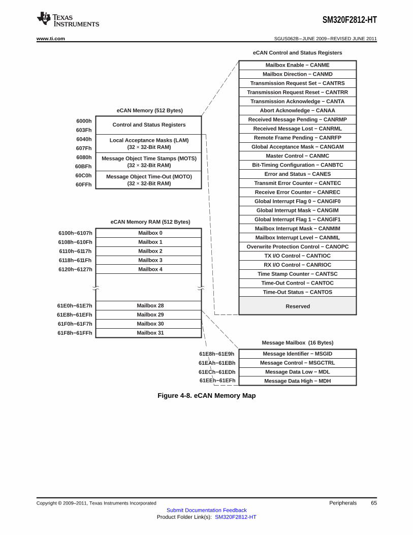
Mailbox Enable − CANME
Mailbox Direction − CANMD
Transmission Request Set − CANTRS
Transmission Request Reset − CANTRR
Transmission Acknowledge − CANT A
Abort Acknowledge − CANAA
Received Message Pending − CANRMP
Received Message Lost − CANRML
Remote Frame Pending − CANRFP
Global Acceptance Mask − CANGAM
Master Control − CANMC
Bit-T iming Configuration − CANBTC
Error and Status − CANES
Transmit Error Counter − CANTEC
Receive Error Counter − CANREC
Global Interrupt Flag 0 − CANGIF0
Global Interrupt Mask − CANGIM
Mailbox Interrupt Mask − CANMIM
Mailbox Interrupt Level − CANMIL
Overwrite Protection Control − CANOPC
TX I/O Control − CANTIOC
RX I/O Control − CANRIOC
Time Stamp Counter − CANTSC
Global Interrupt Flag 1 − CANGIF1
Time-Out Control − CANT OC
Time-Out Status − CANT OS
Reserved
eCAN Control and Status Registers
Message Identifier − MSGID61E8h−61E9h
Message Control − MSGCTRL
Message Data Low − MDL
Message Data High − MDH
Message Mailbox (16 Bytes)
Control and Status Registers6000h
603Fh
Local Acceptance Masks (LAM)(32 × 32-Bit RAM)
6040h
607Fh
6080h
60BFh
60C0h
60FFh
eCAN Memory (512 Bytes)
Message Object T ime Stamps (MOTS)(32 × 32-Bit RAM)
Message Object T ime-Out (MOT O)(32 × 32-Bit RAM)
Mailbox 06100h−6107h
Mailbox 16108h−610Fh
Mailbox 26110h−6117h
Mailbox 36118h−611Fh
eCAN Memory RAM (512 Bytes)
Mailbox 46120h−6127h
Mailbox 2861E0h−61E7h
Mailbox 2961E8h−61EFh
Mailbox 3061F0h−61F7h
Mailbox 3161F8h−61FFh
61EAh−61EBh
61ECh−61EDh
61EEh−61EFh
SM320F2812-HT
www.ti.com SGUS062B–JUNE 2009–REVISED JUNE 2011
Figure 4-8. eCAN Memory Map
Copyright © 2009–2011, Texas Instruments Incorporated Peripherals 65Submit Documentation Feedback
Product Folder Link(s): SM320F2812-HT
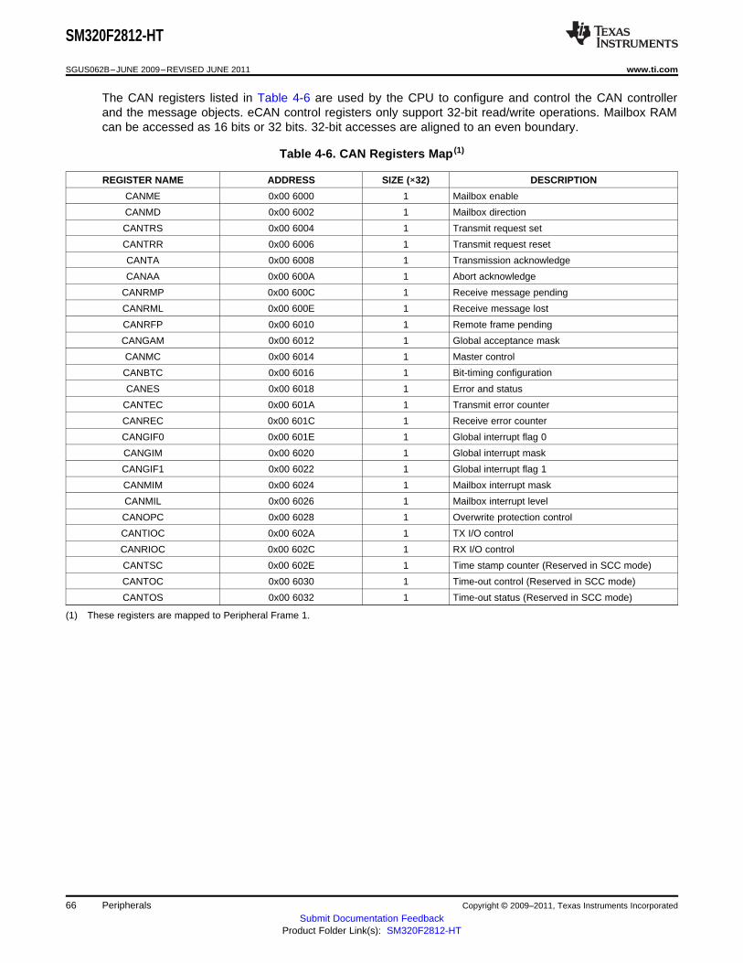
SM320F2812-HT
SGUS062B–JUNE 2009–REVISED JUNE 2011 www.ti.com
The CAN registers listed in Table 4-6 are used by the CPU to configure and control the CAN controllerand the message objects. eCAN control registers only support 32-bit read/write operations. Mailbox RAMcan be accessed as 16 bits or 32 bits. 32-bit accesses are aligned to an even boundary.
Table 4-6. CAN Registers Map (1)
REGISTER NAME ADDRESS SIZE (×32) DESCRIPTION
CANME 0x00 6000 1 Mailbox enable
CANMD 0x00 6002 1 Mailbox direction
CANTRS 0x00 6004 1 Transmit request set
CANTRR 0x00 6006 1 Transmit request reset
CANTA 0x00 6008 1 Transmission acknowledge
CANAA 0x00 600A 1 Abort acknowledge
CANRMP 0x00 600C 1 Receive message pending
CANRML 0x00 600E 1 Receive message lost
CANRFP 0x00 6010 1 Remote frame pending
CANGAM 0x00 6012 1 Global acceptance mask
CANMC 0x00 6014 1 Master control
CANBTC 0x00 6016 1 Bit-timing configuration
CANES 0x00 6018 1 Error and status
CANTEC 0x00 601A 1 Transmit error counter
CANREC 0x00 601C 1 Receive error counter
CANGIF0 0x00 601E 1 Global interrupt flag 0
CANGIM 0x00 6020 1 Global interrupt mask
CANGIF1 0x00 6022 1 Global interrupt flag 1
CANMIM 0x00 6024 1 Mailbox interrupt mask
CANMIL 0x00 6026 1 Mailbox interrupt level
CANOPC 0x00 6028 1 Overwrite protection control
CANTIOC 0x00 602A 1 TX I/O control
CANRIOC 0x00 602C 1 RX I/O control
CANTSC 0x00 602E 1 Time stamp counter (Reserved in SCC mode)
CANTOC 0x00 6030 1 Time-out control (Reserved in SCC mode)
CANTOS 0x00 6032 1 Time-out status (Reserved in SCC mode)
(1) These registers are mapped to Peripheral Frame 1.
66 Peripherals Copyright © 2009–2011, Texas Instruments Incorporated
Submit Documentation FeedbackProduct Folder Link(s): SM320F2812-HT

CLKSRGMcBSP clock rate CLKG ,
1 CLKGDIV= =
+
SM320F2812-HT
www.ti.com SGUS062B–JUNE 2009–REVISED JUNE 2011
4.5 Multichannel Buffered Serial Port (McBSP) Module
The McBSP module has the following features:• Compatible to McBSP in TMS320C54x™/ TMS320C55x™ DSP devices, except the DMA features• Full-duplex communication• Double-buffered data registers which allow a continuous data stream• Independent framing and clocking for receive and transmit• External shift clock generation or an internal programmable frequency shift clock• A wide selection of data sizes including 8/12/16/20/24 or 32-bits• 8-bit data transfers with LSB or MSB first• Programmable polarity for both frame synchronization and data clocks• Highly programmable internal clock and frame generation• Support A-bis mode• Direct interface to industry-standard CODECs, Analog Interface Chips (AICs), and other serially
connected A/D and D/A devices• Works with SPI-compatible devices• Two 16 x 16-level FIFO for Transmit channel• Two 16 x 16-level FIFO for Receive channel
The following application interfaces can be supported on the McBSP:• T1/E1 framers• MVIP switching-compatible and ST-BUS-compliant devices including:
– MVIP framers– H.100 framers– SCSA framers– IOM-2 compliant devices– AC97-compliant devices (the necessary multiphase frame synchronization capability is provided.)– IIS-compliant devices
•where CLKSRG source could be LSPCLK, CLKX, or CLKR. (2)
(2) Serial port performance is limited by I/O buffer switching speed. Internal prescalers must be adjusted such that the peripheral speed isless than the I/O buffer speed limit—20-MHz maximum.
Copyright © 2009–2011, Texas Instruments Incorporated Peripherals 67Submit Documentation Feedback
Product Folder Link(s): SM320F2812-HT

McBSP ReceiveInterrupt Select Logic
DX
DR
Expand Logic
DRR1 Receive Buffer
RX FIFOInterrupt
DRR2 Receive Buffer
RX FIFO Registers
RBR1 RegisterRBR2 Register
McBSP Registersand Control Logic
CLKX
FSX
CLKR
FSR
16
Compand Logic
DXR2 Transmit Buffer
RSR1
XSR2 XSR1
Peripheral Read Bus
16
1616
1616
RSR2
DXR1 Transmit Buffer
16
LSPCLK
MRINT
To CPU
McBSP
RX Interrupt Logic
RX FIFO _15
—
RX FIFO _1
RX FIFO _0
RX FIFO _15
—
RX FIFO _1
RX FIFO _0
McBSP TransmitInterrupt Select Logic
TX FIFOInterrupt
TX FIFO Registers
MXINT
To CPU TX Interrupt Logic
16 16
16
TX FIFO _15
—
TX FIFO _1
TX FIFO _0
TX FIFO _15
—
TX FIFO _1
TX FIFO _0
Peripheral Write Bus
SM320F2812-HT
SGUS062B–JUNE 2009–REVISED JUNE 2011 www.ti.com
Figure 4-9 shows the block diagram of the McBSP module with FIFO, interfaced to the F2812 version ofPeripheral Frame 2.
Figure 4-9. McBSP Module With FIFO
68 Peripherals Copyright © 2009–2011, Texas Instruments Incorporated
Submit Documentation FeedbackProduct Folder Link(s): SM320F2812-HT
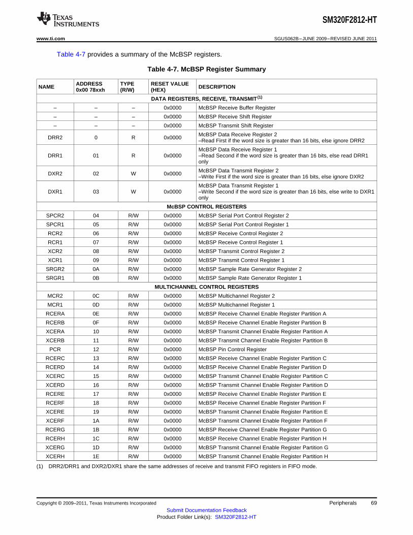
SM320F2812-HT
www.ti.com SGUS062B–JUNE 2009–REVISED JUNE 2011
Table 4-7 provides a summary of the McBSP registers.
Table 4-7. McBSP Register Summary
ADDRESS TYPE RESET VALUENAME DESCRIPTION0x00 78xxh (R/W) (HEX)
DATA REGISTERS, RECEIVE, TRANSMIT (1)
– – – 0x0000 McBSP Receive Buffer Register
– – – 0x0000 McBSP Receive Shift Register
– – – 0x0000 McBSP Transmit Shift Register
McBSP Data Receive Register 2DRR2 0 R 0x0000 –Read First if the word size is greater than 16 bits, else ignore DRR2
McBSP Data Receive Register 1DRR1 01 R 0x0000 –Read Second if the word size is greater than 16 bits, else read DRR1
only
McBSP Data Transmit Register 2DXR2 02 W 0x0000 –Write First if the word size is greater than 16 bits, else ignore DXR2
McBSP Data Transmit Register 1DXR1 03 W 0x0000 –Write Second if the word size is greater than 16 bits, else write to DXR1
only
McBSP CONTROL REGISTERS
SPCR2 04 R/W 0x0000 McBSP Serial Port Control Register 2
SPCR1 05 R/W 0x0000 McBSP Serial Port Control Register 1
RCR2 06 R/W 0x0000 McBSP Receive Control Register 2
RCR1 07 R/W 0x0000 McBSP Receive Control Register 1
XCR2 08 R/W 0x0000 McBSP Transmit Control Register 2
XCR1 09 R/W 0x0000 McBSP Transmit Control Register 1
SRGR2 0A R/W 0x0000 McBSP Sample Rate Generator Register 2
SRGR1 0B R/W 0x0000 McBSP Sample Rate Generator Register 1
MULTICHANNEL CONTROL REGISTERS
MCR2 0C R/W 0x0000 McBSP Multichannel Register 2
MCR1 0D R/W 0x0000 McBSP Multichannel Register 1
RCERA 0E R/W 0x0000 McBSP Receive Channel Enable Register Partition A
RCERB 0F R/W 0x0000 McBSP Receive Channel Enable Register Partition B
XCERA 10 R/W 0x0000 McBSP Transmit Channel Enable Register Partition A
XCERB 11 R/W 0x0000 McBSP Transmit Channel Enable Register Partition B
PCR 12 R/W 0x0000 McBSP Pin Control Register
RCERC 13 R/W 0x0000 McBSP Receive Channel Enable Register Partition C
RCERD 14 R/W 0x0000 McBSP Receive Channel Enable Register Partition D
XCERC 15 R/W 0x0000 McBSP Transmit Channel Enable Register Partition C
XCERD 16 R/W 0x0000 McBSP Transmit Channel Enable Register Partition D
RCERE 17 R/W 0x0000 McBSP Receive Channel Enable Register Partition E
RCERF 18 R/W 0x0000 McBSP Receive Channel Enable Register Partition F
XCERE 19 R/W 0x0000 McBSP Transmit Channel Enable Register Partition E
XCERF 1A R/W 0x0000 McBSP Transmit Channel Enable Register Partition F
RCERG 1B R/W 0x0000 McBSP Receive Channel Enable Register Partition G
RCERH 1C R/W 0x0000 McBSP Receive Channel Enable Register Partition H
XCERG 1D R/W 0x0000 McBSP Transmit Channel Enable Register Partition G
XCERH 1E R/W 0x0000 McBSP Transmit Channel Enable Register Partition H
(1) DRR2/DRR1 and DXR2/DXR1 share the same addresses of receive and transmit FIFO registers in FIFO mode.
Copyright © 2009–2011, Texas Instruments Incorporated Peripherals 69Submit Documentation Feedback
Product Folder Link(s): SM320F2812-HT

SM320F2812-HT
SGUS062B–JUNE 2009–REVISED JUNE 2011 www.ti.com
Table 4-7. McBSP Register Summary (continued)
ADDRESS TYPE RESET VALUENAME DESCRIPTION0x00 78xxh (R/W) (HEX)
FIFO MODE REGISTERS (applicable only in FIFO mode)
FIFO Data Registers (1)
McBSP Data Receive Register 2 – Top of receive FIFODRR2 00 R 0x0000 –Read First FIFO pointers does not advance
McBSP Data Receive Register 1 – Top of receive FIFODRR1 01 R 0x0000 –Read Second for FIFO pointers to advance
McBSP Data Transmit Register 2 – Top of transmit FIFODXR2 02 W 0x0000 –Write First FIFO pointers does not advance
McBSP Data Transmit Register 1 – Top of transmit FIFODXR1 03 W 0x0000 –Write Second for FIFO pointers to advance
FIFO Control Registers
MFFTX 20 R/W 0xA000 McBSP Transmit FIFO Register
MFFRX 21 R/W 0x201F McBSP Receive FIFO Register
MFFCT 22 R/W 0x0000 McBSP FIFO Control Register
MFFINT 23 R/W 0x0000 McBSP FIFO Interrupt Register
MFFST 24 R/W 0x0000 McBSP FIFO Status Register
(1) FIFO pointers advancing is based on order of access to DRR2/DRR1 and DXR2/DXR1 registers.
70 Peripherals Copyright © 2009–2011, Texas Instruments Incorporated
Submit Documentation FeedbackProduct Folder Link(s): SM320F2812-HT

LSPCLK,
(BRR 1) 8+ ·
LSPCLK,
16
6150MHzMax bit rate 9.375 10 b / s
2 8= = ´
´
SM320F2812-HT
www.ti.com SGUS062B–JUNE 2009–REVISED JUNE 2011
4.6 Serial Communications Interface (SCI) Module
The F2812 device include two serial communications interface (SCI) modules. The SCI modules supportdigital communications between the CPU and other asynchronous peripherals that use the standardnon-return-to-zero (NRZ) format. The SCI receiver and transmitter are double-buffered, and each has itsown separate enable and interrupt bits. Both can be operated independently or simultaneously in thefull-duplex mode. To ensure data integrity, the SCI checks received data for break detection, parity,overrun, and framing errors. The bit rate is programmable to over 65 000 different speeds through a 16-bitbaud-select register.
Features of each SCI module include:• Two external pins:
– SCITXD: SCI transmit-output pin– SCIRXD: SCI receive-input pin
NOTEBoth pins can be used as GPIO if not used for SCI.
• Baud rate programmable to 64K different rates
– Baud ratewhen BRR ≠ 0
=
= when BRR = 0
• Data-word format– One start bit– Data-word length programmable from one to eight bits– Optional even/odd/no parity bit– One or two stop bits
• Four error-detection flags: parity, overrun, framing, and break detection• Two wake-up multiprocessor modes: idle-line and address bit• Half- or full-duplex operation• Double-buffered receive and transmit functions• Transmitter and receiver operations can be accomplished through interrupt-driven or polled algorithms
with status flags.– Transmitter: TXRDY flag (transmitter-buffer register is ready to receive another character) andTX
EMPTY flag (transmitter-shift register is empty)– Receiver: RXRDY flag (receiver-buffer register is ready to receive another character), BRKDT flag
(break condition occurred), and RX ERROR flag (monitoring four interrupt conditions)• Separate enable bits for transmitter and receiver interrupts (except BRKDT)
•• NRZ (non-return-to-zero) format• Ten SCI module control registers located in the control register frame beginning at address 7050h
Copyright © 2009–2011, Texas Instruments Incorporated Peripherals 71Submit Documentation Feedback
Product Folder Link(s): SM320F2812-HT

SM320F2812-HT
SGUS062B–JUNE 2009–REVISED JUNE 2011 www.ti.com
NOTEAll registers in this module are 8-bit registers that are connected to Peripheral Frame 2.When a register is accessed, the register data is in the lower byte (7–0), and the upper byte(15–8) is read as zeros. Writing to the upper byte has no effect.
Enhanced features:• Auto baud-detect hardware logic• 16-level transmit/receive FIFO
The SCI port operation is configured and controlled by the registers listed in Table 4-8 and Table 4-9.
Table 4-8. SCI-A Registers (1)
NAME ADDRESS SIZE (×16) DESCRIPTION
SCICCRA 0x00 7050 1 SCI-A Communications Control Register
SCICTL1A 0x00 7051 1 SCI-A Control Register 1
SCIHBAUDA 0x00 7052 1 SCI-A Baud Register, High Bits
SCILBAUDA 0x00 7053 1 SCI-A Baud Register, Low Bits
SCICTL2A 0x00 7054 1 SCI-A Control Register 2
SCIRXSTA 0x00 7055 1 SCI-A Receive Status Register
SCIRXEMUA 0x00 7056 1 SCI-A Receive Emulation Data Buffer Register
SCIRXBUFA 0x00 7057 1 SCI-A Receive Data Buffer Register
SCITXBUFA 0x00 7059 1 SCI-A Transmit Data Buffer Register
SCIFFTXA 0x00 705A 1 SCI-A FIFO Transmit Register
SCIFFRXA 0x00 705B 1 SCI-A FIFO Receive Register
SCIFFCTA 0x00 705C 1 SCI-A FIFO Control Register
SCIPRIA 0x00 705F 1 SCI-A Priority Control Register
(1) Shaded registers are new registers for the FIFO mode.
Table 4-9. SCI-B Registers (1) (2)
NAME ADDRESS SIZE (×16) DESCRIPTION
SCICCRB 0x00 7750 1 SCI-B Communications Control Register
SCICTL1B 0x00 7751 1 SCI-B Control Register 1
SCIHBAUDB 0x00 7752 1 SCI-B Baud Register, High Bits
SCILBAUDB 0x00 7753 1 SCI-B Baud Register, Low Bits
SCICTL2B 0x00 7754 1 SCI-B Control Register 2
SCIRXSTB 0x00 7755 1 SCI-B Receive Status Register
SCIRXEMUB 0x00 7756 1 SCI-B Receive Emulation Data Buffer Register
SCIRXBUFB 0x00 7757 1 SCI-B Receive Data Buffer Register
SCITXBUFB 0x00 7759 1 SCI-B Transmit Data Buffer Register
SCIFFTXB 0x00 775A 1 SCI-B FIFO Transmit Register
SCIFFRXB 0x00 775B 1 SCI-B FIFO Receive Register
SCIFFCTB 0x00 775C 1 SCI-B FIFO Control Register
SCIPRIB 0x00 775F 1 SCI-B Priority Control Register
(1) Shaded registers are new registers for the FIFO mode.(2) Registers in this table are mapped to peripheral bus 16 space. This space only allows 16-bit accesses. 32-bit accesses produce
undefined results.
72 Peripherals Copyright © 2009–2011, Texas Instruments Incorporated
Submit Documentation FeedbackProduct Folder Link(s): SM320F2812-HT

TX FIFO _0
LSPCLK
WUT
Frame Format and Mode
Even/Odd EnableParity
SCI RX Interrupt select logic
BRKDT
RXRDY
SCIRXST.6
SCICTL1.3
8SCICTL2.1
RX/BK INT ENA
SCIRXD
SCIRXST.1
TXENA
SCI TX Interrupt select logic
TX EMPTY
TXRDY
SCICTL2.0
TX INT ENA
SCITXD
RXENA
SCIRXD
RXWAKE
SCICTL1.6
RX ERR INT ENA
TXWAKE
SCITXD
SCICCR.6 SCICCR.5
SCITXBUF.7−0
SCIHBAUD. 15 − 8
Baud RateMSbyteRegister
SCILBAUD. 7 − 0
Transmitter−DataBuffer Register
8 SCICTL2.6
SCICTL2.7
Baud RateLSbyte
Register
RXSHFRegister
TXSHFRegister
SCIRXST.5
1 TX FIFO _1
−−−−−TX FIFO _15
8
TX FIFO registers
TX FIFO
TX InterruptLogic
TXINT
SCIFFTX.14
RX FIFO _15
SCIRXBUF.7−0
Receive DataBuffer registerSCIRXBUF.7−0
−−−−−RX FIFO_1
RX FIFO _0
8
RX FIFO registers
SCICTL1.0
RX InterruptLogic
RXINT
RX FIFO
SCIFFRX.15
RXFFOVF
RX Error
SCIRXST.7
PEFE OERX Error
SCIRXST.4 − 2
To CPU
To CPU
AutoBaud Detect logic
SCICTL1.1
SCIFFENA
Interrupts
Interrupts
SM320F2812-HT
www.ti.com SGUS062B–JUNE 2009–REVISED JUNE 2011
Figure 4-10 shows the SCI module block diagram.
Figure 4-10. Serial Communications Interface (SCI) Module Block Diagram
Copyright © 2009–2011, Texas Instruments Incorporated Peripherals 73Submit Documentation Feedback
Product Folder Link(s): SM320F2812-HT
LSPCLK,
(SPIBRR 1)+
LSPCLK,
4
SM320F2812-HT
SGUS062B–JUNE 2009–REVISED JUNE 2011 www.ti.com
4.7 Serial Peripheral Interface (SPI) Module
The F2812 device includes the four-pin serial peripheral interface (SPI) module. The SPI is a high-speed,synchronous serial I/O port that allows a serial bit stream of programmed length (one to sixteen bits) to beshifted into and out of the device at a programmable bit-transfer rate. Normally, the SPI is used forcommunications between the DSP controller and external peripherals or another processor. Typicalapplications include external I/O or peripheral expansion through devices such as shift registers, displaydrivers, and ADCs. Multidevice communications are supported by the master/slave operation of the SPI.
The SPI module features include:• Four external pins:
– SPISOMI: SPI slave-output/master-input pin– SPISIMO: SPI slave-input/master-output pin– SPISTE: SPI slave transmit-enable pin– SPICLK: SPI serial-clock pin
NOTEAll four pins can be used as GPIO, if the SPI module is not used.
• Two operational modes: master and slave• Baud rate: 125 different programmable rates
– Baud ratewhen BRR ≠ 0
=
= when BRR = 0, 1, 2, 3
Serial port performance is limited by I/O buffer switching speed. Internal prescalers must be adjustedsuch that the peripheral speed is less than the I/O buffer speed limit—20 MHz maximum.
• Data word length: one to sixteen data bits• Four clocking schemes (controlled by clock polarity and clock phase bits) include:
– Falling edge without phase delay: SPICLK active-high. SPI transmits data on the falling edge of theSPICLK signal and receives data on the rising edge of the SPICLK signal.
– Falling edge with phase delay: SPICLK active-high. SPI transmits data one half-cycle ahead of thefalling edge of the SPICLK signal and receives data on the falling edge of the SPICLK signal.
– Rising edge without phase delay: SPICLK inactive-low. SPI transmits data on the rising edge of theSPICLK signal and receives data on the falling edge of the SPICLK signal.
– Rising edge with phase delay: SPICLK inactive-low. SPI transmits data one half-cycle ahead of thefalling edge of the SPICLK signal and receives data on the rising edge of the SPICLK signal.
• Simultaneous receive and transmit operation (transmit function can be disabled in software)• Transmitter and receiver operations are accomplished through either interrupt-driven or polled
algorithms.• Nine SPI module control registers: Located in control register frame beginning at address 7040h.
NOTEAll registers in this module are 16-bit registers that are connected to Peripheral Frame 2.When a register is accessed, the register data is in the lower byte (7–0), and the upper byte(15–8) is read as zeros. Writing to the upper byte has no effect.
74 Peripherals Copyright © 2009–2011, Texas Instruments Incorporated
Submit Documentation FeedbackProduct Folder Link(s): SM320F2812-HT

SM320F2812-HT
www.ti.com SGUS062B–JUNE 2009–REVISED JUNE 2011
Enhanced feature:• 16-level transmit/receive FIFO• Delayed transmit control
The SPI port operation is configured and controlled by the registers listed in Table 4-10.
Table 4-10. SPI Registers (1)
NAME ADDRESS SIZE (×16) DESCRIPTION
SPICCR 0x00 7040 1 SPI Configuration Control Register
SPICTL 0x00 7041 1 SPI Operation Control Register
SPISTS 0x00 7042 1 SPI Status Register
SPIBRR 0x00 7044 1 SPI Baud Rate Register
SPIRXEMU 0x00 7046 1 SPI Receive Emulation Buffer Register
SPIRXBUF 0x00 7047 1 SPI Serial Input Buffer Register
SPITXBUF 0x00 7048 1 SPI Serial Output Buffer Register
SPIDAT 0x00 7049 1 SPI Serial Data Register
SPIFFTX 0x00 704A 1 SPI FIFO Transmit Register
SPIFFRX 0x00 704B 1 SPI FIFO Receive Register
SPIFFCT 0x00 704C 1 SPI FIFO Control Register
SPIPRI 0x00 704F 1 SPI Priority Control Register
(1) The above registers are mapped to Peripheral Frame 2. This space only allows 16-bit accesses. 32-bit accesses produce undefinedresults.
Copyright © 2009–2011, Texas Instruments Incorporated Peripherals 75Submit Documentation Feedback
Product Folder Link(s): SM320F2812-HT

S
SPICTL.0
SPI INT FLAGSPI INT
ENA
SPISTS.6
S
ClockPolarity
Talk
LSPCLK
456 123 0
0123
SPI Bit Rate
State Control
SPIRXBUFBuffer Register
ClockPhase
ReceiverOverrun Flag
SPICTL.4
OverrunINT ENA
SPICCR.3 − 0
SPIBRR.6 − 0 SPICCR.6 SPICTL.3
SPIDAT.15 − 0
SPICTL.1
M
S
M
Master/Slave
SPISTS.7
SPIDATData Register
M
S
SPICTL.2SPI Char
SPISIMO
SPISOMI
SPICLK
SW2
S
M
M
S
SW3
To CPU
M
SW1
SPITXBUFBuffer Register
RX FIFO _0RX FIFO _1
−−−−−RX FIFO _15
TX FIFO registers
TX FIFO _0TX FIFO _1−−−−−TX FIFO _15
RX FIFO registers
16
16
16
TX InterruptLogic
RX InterruptLogic
SPIINT/SPIRXINT
SPITXINT
SPIFFOVF FLAG
SPIFFRX.15
16
TX FIFO Interrupt
RX FIFO Interrupt
SPIRXBUF
SPITXBUF
SPIFFTX.14
SPIFFENA
SPISTE†
† SPISTE is driven low by the master for a slave device.
SM320F2812-HT
SGUS062B–JUNE 2009–REVISED JUNE 2011 www.ti.com
Figure 4-11 is a block diagram of the SPI in slave mode.
Figure 4-11. Serial Peripheral Interface Module Block Diagram (Slave Mode)
76 Peripherals Copyright © 2009–2011, Texas Instruments Incorporated
Submit Documentation FeedbackProduct Folder Link(s): SM320F2812-HT

SM320F2812-HT
www.ti.com SGUS062B–JUNE 2009–REVISED JUNE 2011
4.8 GPIO MUX
The GPIO Mux registers are used to select the operation of shared pins on the F2812 device. The pinscan be individually selected to operate as Digital I/O or connected to Peripheral I/O signals (via theGPxMUX registers). If selected for Digital I/O mode, registers are provided to configure the pin direction(via the GPxDIR registers) and to qualify the input signal to remove unwanted noise (via the GPxQUAL)registers). Table 4-11 lists the GPIO Mux Registers.
Table 4-11. GPIO Mux Registers (1) (2) (3)
NAME ADDRESS SIZE (×16) REGISTER DESCRIPTION
GPAMUX 0x00 70C0 1 GPIO A Mux Control Register
GPADIR 0x00 70C1 1 GPIO A Direction Control Register
GPAQUAL 0x00 70C2 1 GPIO A Input Qualification Control Register
reserved 0x00 70C3 1
GPBMUX 0x00 70C4 1 GPIO B Mux Control Register
GPBDIR 0x00 70C5 1 GPIO B Direction Control Register
GPBQUAL 0x00 70C6 1 GPIO B Input Qualification Control Register
reserved 0x00 70C7 1
reserved 0x00 70C8 1
reserved 0x00 70C9 1
reserved 0x00 70CA 1
reserved 0x00 70CB 1
GPDMUX 0x00 70CC 1 GPIO D Mux Control Register
GPDDIR 0x00 70CD 1 GPIO D Direction Control Register
GPDQUAL 0x00 70CE 1 GPIO D Input Qualification Control Register
reserved 0x00 70CF 1
GPEMUX 0x00 70D0 1 GPIO E Mux Control Register
GPEDIR 0x00 70D1 1 GPIO E Direction Control Register
GPEQUAL 0x00 70D2 1 GPIO E Input Qualification Control Register
reserved 0x00 70D3 1
GPFMUX 0x00 70D4 1 GPIO F Mux Control Register
GPFDIR 0x00 70D5 1 GPIO F Direction Control Register
reserved 0x00 70D6 1
reserved 0x00 70D7 1
GPGMUX 0x00 70D8 1 GPIO G Mux Control Register
GPGDIR 0x00 70D9 1 GPIO G Direction Control Register
reserved 0x00 70DA 1
reserved 0x00 70DB 1
0x00 70DCreserved 40x00 70DF
(1) Reserved locations returns undefined values and writes is ignored.(2) Not all inputs support input signal qualification.(3) These registers are EALLOW protected. This prevents spurious writes from overwriting the contents and corrupting the system.
If configured for Digital I/O mode, additional registers are provided for setting individual I/O signals (via theGPxSET registers), for clearing individual I/O signals (via the GPxCLEAR registers), for toggling individualI/O signals (via the GPxTOGGLE registers), or for reading/writing to the individual I/O signals (via theGPxDAT registers). Table 4-12 lists the GPIO Data Registers. For more information, see theTMS320x281x System Control and Interrupts Reference Guide (SPRU078).
Copyright © 2009–2011, Texas Instruments Incorporated Peripherals 77Submit Documentation Feedback
Product Folder Link(s): SM320F2812-HT

SM320F2812-HT
SGUS062B–JUNE 2009–REVISED JUNE 2011 www.ti.com
Table 4-12. GPIO Data Registers (1) (2)
NAME ADDRESS SIZE (×16) REGISTER DESCRIPTION
GPADAT 0x00 70E0 1 GPIO A Data Register
GPASET 0x00 70E1 1 GPIO A Set Register
GPACLEAR 0x00 70E2 1 GPIO A Clear Register
GPATOGGLE 0x00 70E3 1 GPIO A Toggle Register
GPBDAT 0x00 70E4 1 GPIO B Data Register
GPBSET 0x00 70E5 1 GPIO B Set Register
GPBCLEAR 0x00 70E6 1 GPIO B Clear Register
GPBTOGGLE 0x00 70E7 1 GPIO B Toggle Register
reserved 0x00 70E8 1
reserved 0x00 70E9 1
reserved 0x00 70EA 1
reserved 0x00 70EB 1
GPDDAT 0x00 70EC 1 GPIO D Data Register
GPDSET 0x00 70ED 1 GPIO D Set Register
GPDCLEAR 0x00 70EE 1 GPIO D Clear Register
GPDTOGGLE 0x00 70EF 1 GPIO D Toggle Register
GPEDAT 0x00 70F0 1 GPIO E Data Register
GPESET 0x00 70F1 1 GPIO E Set Register
GPECLEAR 0x00 70F2 1 GPIO E Clear Register
GPETOGGLE 0x00 70F3 1 GPIO E Toggle Register
GPFDAT 0x00 70F4 1 GPIO F Data Register
GPFSET 0x00 70F5 1 GPIO F Set Register
GPFCLEAR 0x00 70F6 1 GPIO F Clear Register
GPFTOGGLE 0x00 70F7 1 GPIO F Toggle Register
GPGDAT 0x00 70F8 1 GPIO G Data Register
GPGSET 0x00 70F9 1 GPIO G Set Register
GPGCLEAR 0x00 70FA 1 GPIO G Clear Register
GPGTOGGLE 0x00 70FB 1 GPIO G Toggle Register
0x00 70FCreserved 40x00 70FF
(1) Reserved location returns undefined values and writes are ignored.(2) These registers are NOT EALLOW protected. The above registers are typically accessed regularly by the user.
78 Peripherals Copyright © 2009–2011, Texas Instruments Incorporated
Submit Documentation FeedbackProduct Folder Link(s): SM320F2812-HT

Peripheral I/O
MUX
0 1
MUX
10
PIN
Internal (Pullup or Pulldown)
Digital I/O
XRS
High-ImpedanceEnable (1)
High-Impedance
Control
GPxDIRRegister Bit
GPxMUXRegister Bit
GPxQUALRegister
GPxDAT/SET/CLEAR/TOGGLERegister Bit(s)
Input Qualification SYSCLKOUT
SM320F2812-HT
www.ti.com SGUS062B–JUNE 2009–REVISED JUNE 2011
Figure 4-12 shows how the various register bits select the various modes of operation for GPIO function.
A. In the GPIO mode, when the GPIO pin is configured for output operation, reading the GPxDAT data register onlygives the value written, not the value at the pin. In the peripheral mode, the state of the pin can be read through theGPxDAT register, provided the corresponding direction bit is zero (input mode).
B. Some selected input signals are qualified by the SYSCLKOUT. The GPxQUAL register specifies the qualificationsampling period. The sampling window is 6 samples wide and the output is only changed when all samples are thesame (all 0's or all 1's). This feature removes unwanted spikes from the input signal.
Figure 4-12. GPIO/Peripheral Pin Multiplexing
NOTEThe input function of the GPIO pin and the input path to the peripheral are always enabled. Itis the output function of the GPIO pin that is multiplexed with the output path of the primary(peripheral) function. Since the output buffer of a pin connects back to the input buffer, anyGPIO signal present at the pin is propagated to the peripheral module as well. Therefore,when a pin is configured for GPIO operation, the corresponding peripheral functionality (andinterrupt-generating capability) must be disabled. Otherwise, interrupts may be inadvertentlytriggered. This is especially critical when the PDPINTA and PDPINTB pins are used as GPIOpins, since a value of zero for GPDDAT.0 or GPDDAT.5 (PDPINTx) puts PWM pins in ahigh-impedance state. The CxTRIP and TxCTRIP pins also put the corresponding PWM pinsin high impedance, if they are driven low (as GPIO pins) and bit EXTCONx.0 = 1.
Copyright © 2009–2011, Texas Instruments Incorporated Peripherals 79Submit Documentation Feedback
Product Folder Link(s): SM320F2812-HT
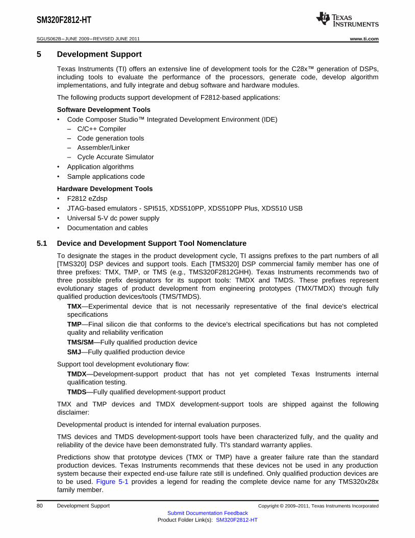
SM320F2812-HT
SGUS062B–JUNE 2009–REVISED JUNE 2011 www.ti.com
5 Development Support
Texas Instruments (TI) offers an extensive line of development tools for the C28x™ generation of DSPs,including tools to evaluate the performance of the processors, generate code, develop algorithmimplementations, and fully integrate and debug software and hardware modules.
The following products support development of F2812-based applications:
Software Development Tools• Code Composer Studio™ Integrated Development Environment (IDE)
– C/C++ Compiler– Code generation tools– Assembler/Linker– Cycle Accurate Simulator
• Application algorithms• Sample applications code
Hardware Development Tools• F2812 eZdsp• JTAG-based emulators - SPI515, XDS510PP, XDS510PP Plus, XDS510 USB• Universal 5-V dc power supply• Documentation and cables
5.1 Device and Development Support Tool Nomenclature
To designate the stages in the product development cycle, TI assigns prefixes to the part numbers of all[TMS320] DSP devices and support tools. Each [TMS320] DSP commercial family member has one ofthree prefixes: TMX, TMP, or TMS (e.g., TMS320F2812GHH). Texas Instruments recommends two ofthree possible prefix designators for its support tools: TMDX and TMDS. These prefixes representevolutionary stages of product development from engineering prototypes (TMX/TMDX) through fullyqualified production devices/tools (TMS/TMDS).
TMX—Experimental device that is not necessarily representative of the final device's electricalspecificationsTMP—Final silicon die that conforms to the device's electrical specifications but has not completedquality and reliability verificationTMS/SM—Fully qualified production deviceSMJ—Fully qualified production device
Support tool development evolutionary flow:TMDX—Development-support product that has not yet completed Texas Instruments internalqualification testing.TMDS—Fully qualified development-support product
TMX and TMP devices and TMDX development-support tools are shipped against the followingdisclaimer:
Developmental product is intended for internal evaluation purposes.
TMS devices and TMDS development-support tools have been characterized fully, and the quality andreliability of the device have been demonstrated fully. TI's standard warranty applies.
Predictions show that prototype devices (TMX or TMP) have a greater failure rate than the standardproduction devices. Texas Instruments recommends that these devices not be used in any productionsystem because their expected end-use failure rate still is undefined. Only qualified production devices areto be used. Figure 5-1 provides a legend for reading the complete device name for any TMS320x28xfamily member.
80 Development Support Copyright © 2009–2011, Texas Instruments Incorporated
Submit Documentation FeedbackProduct Folder Link(s): SM320F2812-HT
PREFIX
SM 320 F 2812 HFG
TMX = experimental deviceTMP = prototype deviceTMS = qualified deviceSM = commercial processingSMJ = MIL-PRF-38535 (QML)
DEVICE FAMILY
320 = TMS320 DSP Family
TECHNOLOGY
PACKAGE TYPE†
HFG = 172-pin CQFPKGD = Die
DEVICE
2810
TEMPERATURE RANGE
M
S = -55°C to 220°C
F = Flash EEPROM (1.8-V/1.9-V Core/3.3-V I/O)
C = ROM (1.8-V/1.9-V Core/3.3-V I/O)
28112812
†Not all combinations of processing options, temperature ranges and packages are available.
CQFP = Ceramic Quad Flatpack
SM320F2812-HT
www.ti.com SGUS062B–JUNE 2009–REVISED JUNE 2011
Figure 5-1. 28x Device Nomenclature
5.2 Documentation Support
Extensive documentation supports all of the TMS320E DSP family generations of devices from productannouncement through applications development. The types of documentation available include: datasheets and data manuals, with design specifications; and hardware and software applications. Usefulreference documentation includes:
TMS320C28x DSP CPU and Instruction Set Reference Guide (SPRU430) describes the centralprocessing unit (CPU) and the assembly language instructions of the TMS320C28x™ fixed-point digitalsignal processors (DSPs). It also describes emulation features available on these DSPs.
TMS320x281x Analog-to-Digital Converter (ADC) Reference Guide (SPRU060) describes the ADCmodule. The module is a 12-bit pipelined ADC. The analog circuits of this converter, referred to as thecore in this document, include the front-end analog multiplexers (MUXs), sample-and-hold (S/H) circuits,the conversion core, voltage regulators, and other analog supporting circuits. Digital circuits, referred to asthe wrapper in this document, include programmable conversion sequencer, result registers, interface toanalog circuits, interface to device peripheral bus, and interface to other on-chip modules.
TMS320x281x Boot ROM Reference Guide (SPRU095) describes the purpose and features of thebootloader (factory-programmed boot-loading software). It also describes other contents of the deviceon-chip boot ROM and identifies where all of the information is located within that memory.
TMS320x281x Event Manager (EV) Reference Guide (SPRU065) describes the EV modules thatprovide a broad range of functions and features that are particularly useful in motion control and motorcontrol applications. The EV modules include general-purpose (GP) timers, full-compare/PWM units,capture units, and quadrature-encoder pulse (QEP) circuits.
TMS320x281x External Interface (XINTF) Reference Guide (SPRU067) describes the external interface(XINTF) of the 281x digital signal processors (DSPs).
TMS320x281x Multi-channel Buffered Serial Ports (McBSPs) Reference Guide (SPRU061) describesthe McBSP) available on the 281x devices. The McBSPs allow direct interface between a DSP and otherdevices in a system.
TMS320x281x System Control and Interrupts Reference Guide (SPRU078) describes the variousinterrupts and system control features of the 281x digital signal processors (DSPs).
Copyright © 2009–2011, Texas Instruments Incorporated Development Support 81Submit Documentation Feedback
Product Folder Link(s): SM320F2812-HT

SM320F2812-HT
SGUS062B–JUNE 2009–REVISED JUNE 2011 www.ti.com
TMS320x281x, 280x Enhanced Controller Area Network (eCAN) Reference Guide (SPRU074)describes the eCAN that uses established protocol to communicate serially with other controllers inelectrically noisy environments. With 32 fully configurable mailboxes and time-stamping feature, the eCANmodule provides a versatile and robust serial communication interface. The eCAN module implemented inthe C28x DSP is compatible with the CAN 2.0B standard (active).
TMS320x281x, 280x Peripheral Reference Guide (SPRU566) describes the peripheral reference guidesof the 28x digital signal processors (DSPs).
TMS320x281x, 280x Serial Communication Interface (SCI) Reference Guide (SPRU051) describes theSCI that is a two-wire asynchronous serial port, commonly known as a UART. The SCI modules supportdigital communications between the CPU and other asynchronous peripherals that use the standardnon-return-to-zero (NRZ) format.
TMS320x281x, 280x Serial Peripheral Interface (SPI) Reference Guide (SPRU059) describes the SPI –a high-speed synchronous serial input/output (I/O) port that allows a serial bit stream of programmedlength (one to sixteen bits) to be shifted into and out of the device at a programmed bit-transfer rate. TheSPI is used for communications between the DSP controller and external peripherals or another controller.
3.3 V DSP for Digital Motor Control Application Report (SPRA550). New generations of motor controldigital signal processors (DSPs) lower their supply voltages from 5 V to 3.3 V to offer higher performanceat lower cost. Replacing traditional 5-V digital control circuitry by 3.3-V designs introduce no additionalsystem cost and no significant complication in interfacing with TTL and CMOS compatible components, aswell as with mixed voltage ICs such as power transistor gate drivers. Just like 5-V based designs, goodengineering practice should be exercised to minimize noise and EMI effects by proper component layoutand PCB design when 3.3-V DSP, ADC, and digital circuitry are used in a mixed signal environment, withhigh and low voltage analog and switching signals, such as a motor control system. In addition, softwaretechniques such as Random PWM method can be used by special features of the Texas Instruments (TI)TMS320x24xx DSP controllers to significantly reduce noise effects caused by EMI radiation.
This application report reviews designs of 3.3-V DSP versus 5-V DSP for low HP motor controlapplications. The application report first describes a scenario of a 3.3-V-only motor controller indicatingthat for most applications, no significant issue of interfacing between 3.3 V and 5 V exists. Cost-effective3.3-V – 5-V interfacing techniques are then discussed for the situations where such interfacing is needed.On-chip 3.3-V ADC versus 5-V ADC is also discussed. Sensitivity and noise effects in 3.3-V and 5-V ADCconversions are addressed. Guidelines for component layout and printed circuit board (PCB) design thatcan reduce system's noise and EMI effects are summarized in the last section.
The TMS320C28x Instruction Set Simulator Technical Overview (SPRU608) describes the simulator,available within the Code Composer Studio for TMS320C2000 IDE, that simulates the instruction set ofthe C28x core.
TMS320C28x DSP/BIOS Application Programming Interface (API) Reference Guide (SPRU625)describes development using DSP/BIOS.
TMS320C28x Assembly Language Tools User's Guide (SPRU513) describes the assembly languagetools (assembler and other tools used to develop assembly language code), assembler directives, macros,common object file format, and symbolic debugging directives for the TMS320C28x™ device.
TMS320C28x Optimizing C Compiler User's Guide (SPRU514) describes the TMS320C28x™ C/C++compiler. This compiler accepts ANSI standard C/C++ source code and produces TMS320™ DSPassembly language source code for the TMS320C28x device.
A series of DSP textbooks is published by Prentice-Hall and John Wiley & Sons to support digital signalprocessing research and education. The TMS320™ DSP newsletter, Details on Signal Processing, ispublished quarterly and distributed to update TMS320™ DSP customers on product information.
Updated information on the TMS320™ DSP controllers can be found on the worldwide web at:http://www.ti.com.
82 Development Support Copyright © 2009–2011, Texas Instruments Incorporated
Submit Documentation FeedbackProduct Folder Link(s): SM320F2812-HT

SM320F2812-HT
www.ti.com SGUS062B–JUNE 2009–REVISED JUNE 2011
To send comments regarding this TMS320F281x/TMS320C281x data manual (SPRS174), use thecommentsatbooks.sc.ti.com email address, which is a repository for feedback. For questions and support,contact the Product Information Center listed at http://www.ti.com/sc/docs/pic/home.htm.
Copyright © 2009–2011, Texas Instruments Incorporated Development Support 83Submit Documentation Feedback
Product Folder Link(s): SM320F2812-HT

SM320F2812-HT
SGUS062B–JUNE 2009–REVISED JUNE 2011 www.ti.com
6 Electrical Specifications
This section provides the absolute maximum ratings and the recommended operating conditions for theSM/SMJ320F2812 DSP.
6.1 Absolute Maximum Ratings
Unless otherwise noted, the list of absolute maximum ratings are specified over operating temperatureranges. Stresses beyond those listed under Absolute Maximum Ratings may cause permanent damage tothe device. These are stress ratings only, and functional operation of the device at these or any otherconditions beyond those indicated under Section 6.2 is not implied. Exposure to absolute-maximum-ratedconditions for extended periods may affect device reliability. All voltage values are with respect to VSS.
xxxVALUE UNIT
Supply voltage range, VDDIO, VDDA1, VDDA2, VDDAIO, and –0.3 to 4.6 VAVDDREFBG
Supply voltage range, VDD, VDD1 –0.5 to 2.5 V
VDD3VFL range –0.3 to 4.6 V
Input voltage range, VIN –0.3 to 4.6 V
Output voltage range, VO –0.3 to 4.6 V
Input clamp current, IIK (VIN < 0 or VIN > VDDIO) (1) ±20 mA
Output clamp current, IOK (VO < 0 or VO > VDDIO) ±20 mA
Operating ambient temperature range, TA(2) S Temp –55 to 220 °C
(1) Continuous clamp current per pin is ±2 mA(2) Long-term high-temperature storage and/or extended use at maximum temperature conditions may result in a reduction of overall device
life.
84 Electrical Specifications Copyright © 2009–2011, Texas Instruments Incorporated
Submit Documentation FeedbackProduct Folder Link(s): SM320F2812-HT

SM320F2812-HT
www.ti.com SGUS062B–JUNE 2009–REVISED JUNE 2011
6.2 Recommended Operating ConditionsSee (1)
MIN NOM MAX UNIT
VDDIO Device supply voltage, I/O 3.14 3.3 3.47 V
1.8 V (135 MHz) 1.71 1.8 1.89VDD, VDD1 Device supply voltage, CPU V
1.9 V (150 MHz) 1.81 1.9 2
VSS Supply ground 0 V
VDDA1, VDDA2, ADC supply voltage 3.14 3.3 3.47 VAVDDREFBG, VDDAIO
Flash programming supplyVDD3VFL 3.14 3.3 3.47 Vvoltage
VDD = 1.9 V ± 5% 2 150Device clock frequencyfSYSCLKOUT MHz(system clock) VDD = 1.8 V ± 5% 2 135
All inputs except XCLKIN 2 VDDIOVIH High-level input voltage V
XCLKIN (at 50 μA max) 0.7VDD VDD
All inputs except XCLKIN 0.8VIL Low-level input voltage V
XCLKIN (at 50 μA max) 0.3VDD
High-level output source All I/Os except Group 2 –4IOH current, mA
Group 2 (2) –8VOH = 2.4 V
All I/Os except Group 2 4Low-level output sink current,IOL mAVOL = VOL MAX Group 2 (2) 8
TA Ambient temperature –55 25 220 °C
(1) See Section 6.7 for power sequencing of VDDIO, VDDAIO, VDD, VDDA1/VDDA2/AVDDREFBG, and VDD3VFL.(2) Group 2 pins are as follows: XINTF pins, PDPINTA, TDO, XCLKOUT, XF, EMU0, and EMU1.
In Revision C, EVA (GPIOA0–GPIOA15) and GPIOD0 are 4 mA drive.
6.3 Electrical CharacteristicsOver recommended operating conditions (unless otherwise noted) (1)
PARAMETER TEST CONDITIONS MIN TYP MAX UNIT
IOH = IOHMAX 2.4VOH High-level output voltage VVDDIOIOH = 50 μA – 0.2
VOL Low-level output voltage IOL = IOLMAX 0.4 V
All I/Os (2) (including XRS) –80 –140 –190VDDIO = 3.3 V,Input except EVBWith pullup VIN = 0 VIIL current μAGPIOB/EVB –13 –25 –35(low level)With pulldown VDDIO = 3.3 V, VIN = 0 V ±2
Input With pullup VDDIO = 3.3 V, VIN = VDD ±2currentIIH μAVDDIO = 3.3 V,(high With pulldown (3) 28 50 80VIN = VDDlevel)
Output current,IOZ VO = VDDIO or 0 V ±2 μAhigh-impedance state (off-state)
CI Input capacitance 7 pF
Co Output capacitance 7 pF
(1) Minimum and maximum parameters are characterized for operation at TA = 220°C unless otherwise noted, but may not be productiontested at that temperature. Production test limits with statistical guardbands are used to ensure high temperature performance.
(2) The following pins have no internal PU/PD: GPIOE0, GPIOE1, GPIOF0, GPIOF1, GPIOF2, GPIOF3, GPIOF12, GPIOG4, and GPIOG5.(3) The following pins have an internal pulldown: XMP/MC, TESTSEL, and TRST.
Copyright © 2009–2011, Texas Instruments Incorporated Electrical Specifications 85Submit Documentation Feedback
Product Folder Link(s): SM320F2812-HT

1.00E+06
1.00E+05
1.00E+04
1.00E+03
1.00E+0270 150 200 220
Die Junction Temperature (°C)
Ho
urs
SM320F2812-HT
SGUS062B–JUNE 2009–REVISED JUNE 2011 www.ti.com
Figure 6-1. SM320F2812-HT Life Expectancy Curve
Notes:
1. See data sheet for absolute maximum and minimum recommended operating conditions.
2. Silicon operating life design goal is 10 years at 105°C junction temperature (does not include packageinterconnect life).
86 Electrical Specifications Copyright © 2009–2011, Texas Instruments Incorporated
Submit Documentation FeedbackProduct Folder Link(s): SM320F2812-HT

SM320F2812-HT
www.ti.com SGUS062B–JUNE 2009–REVISED JUNE 2011
6.4 Current Consumption by Power-Supply Pins Over Recommended OperatingConditions During Low-Power Modes at 150-MHz SYSCLKOUT
TA = –55°C to 125°C TA = 220°C
MODE TEST CONDITIONS IDD IDDIO IDD3VFL IDDA(1) IDD IDDIO IDD3VFL IDDA
(1)
TYP MAX(2) TYP MAX(2) TYP MAX(2) TYP MAX(2) TYP MAX TYP MAX TYP MAX TYP MAX
All peripheral clocksare enabled. AllPWM pins aretoggled at 100 kHz.Data is continuouslytransmitted out of the
Operational SCIA, SCIB, and 195 mA 230 mA 15 mA 30 mA 40 mA 45 mA 40 mA 50 mA 275 mA 330 mA 17 mA 30 mA 45 mA 50 mA 40 mA 52 mACAN ports. Thehardware multiplier isexercised.Code is running outof flash with 5wait-states.
–Flash is powereddown–XCLKOUT is turned
IDLE 125 mA 150 mA 5 mA 10 mA 2 μA 4 μA 1 μA 35 μA 200 mA 10 mA 56 μA 100 μA 320 μA 450 μAoff–All peripheral clocksare on, except ADC
–Flash is powereddown–Peripheral clocks
STANDBY are turned off 5 mA 10 mA 5 μA 20 μA 2 μA 4 μA 1 μA 35 μA 27 mA 40 mA 160 μA 200 μA 56 μA 100 μA 320 μA 450 μA–Pins without aninternal PU/PD aretied high/low
–Flash is powereddown–Peripheral clocksare turned off
HALT –Pins without an 70 μA 5 μA 20 μA 2 μA 4 μA 1μA 35 μA 9.8 mA 160 μA 200 μA 56 μA 100 μA 320 μA 450 μAinternal PU/PD aretied high/low– Input clock isdisabled
(1) IDDA includes current into VDDA1, VDDA2, VDD1, AVDDREFBG , and VDDAIO pins.(2) MAX numbers are at 125°C, and max voltage (VDD = 2.0 V; VDDIO, VDD3VFL, VDDA = 3.6 V).
xxx
NOTEHALT and STANDBY modes cannot be used when the PLL is disabled.
Copyright © 2009–2011, Texas Instruments Incorporated Electrical Specifications 87Submit Documentation Feedback
Product Folder Link(s): SM320F2812-HT

0
50
100
150
200
250
0 20 40 60 80 100 120 140 160
SYSCLKOUT (MHz)
IDD IDDIO IDD3VFL IDDA Total 3.3−V current
Cur
rent
(m
A)
0
100
200
300
400
500
600
700
0 20 40 60 80 100 120 140 160
SYSCLKOUT (MHz)
TOTAL POWER
Po
wer
(m
W)
SM320F2812-HT
SGUS062B–JUNE 2009–REVISED JUNE 2011 www.ti.com
6.5 Current Consumption Graphs
A. Test conditions are as defined in Table 6-5 for operational currents under nominal process voltage and temperatureconditions.
B. IDD represents the total current drawn from the 1.8-V rail (VDD). It includes a trivial amount of current (<1 mA) drawnby VDD1.
C. IDDA represents the current drawn by VDDA1 and VDDA2 rails.D. Total 3.3-V current is the sum of IDDIO, IDD3VFL, and IDDA. It includes a trivial amount of current (<1 mA) drawn by
VDDAIO.
Figure 6-2. Typical Current Consumption Over Frequency
Figure 6-3. Typical Power Consumption Over Frequency
88 Electrical Specifications Copyright © 2009–2011, Texas Instruments Incorporated
Submit Documentation FeedbackProduct Folder Link(s): SM320F2812-HT

SM320F2812-HT
www.ti.com SGUS062B–JUNE 2009–REVISED JUNE 2011
6.6 Reducing Current Consumption
28x DSPs incorporate a unique method to reduce the device current consumption. A reduction in currentconsumption can be achieved by turning off the clock to any peripheral module which is not used in agiven application. Table 6-1 indicates the typical reduction in current consumption achieved by turning offthe clocks to various peripherals.
Table 6-1. Typical Current Consumption by Various Peripherals (at 150 MHz) (1)(2)
PERIPHERAL MODULE IDD CURRENT REDUCTION (mA)
eCAN 12
EVA 6
EVB 6
ADC 8 (3)
SCI 4
SPI 5
McBSP 13
(1) All peripheral clocks are disabled upon reset. Writing to/reading from peripheral registers ispossible only after the peripheral clocks are turned on.
(2) Not production tested.(3) This number represents the current drawn by the digital portion of the ADC module. Turning off the
clock to the ADC module results in the elimination of the current drawn by the analog portion of theADC (ICCA) as well.
6.7 Power Sequencing Requirements
SM320F2812 silicon requires dual voltages (1.8-V or 1.9-V and 3.3-V) to power up the CPU, Flash, ROM,ADC, and the I/Os. To ensure the correct reset state for all modules during power up, there are somerequirements to be met while powering up/powering down the device. The current F2812 silicon referenceschematics (Spectrum Digital Incorporated eZdsp. board) suggests two options for the power sequencingcircuit.• Option 1: In this approach, an external power sequencing circuit enables VDDIO first, then VDD and
VDD1 (1.8 V or 1.9 V). After 1.8 V (or 1.9 V) ramps, the 3.3 V for Flash (VDD3VFL) and ADC(VDDA1/VDDA2/AVDDREFBG) modules are ramped up. While option 1 is still valid, TI has simplified therequirement. Option 2 is the recommended approach.
• Option 2: Enable power to all 3.3-V supply pins (VDDIO, VDD3VFL, VDDA1/VDDA2/VDDAIO/AVDDREFBG) andthen ramp 1.8 V (or 1.9 V) (VDD/VDD1) supply pins. 1.8 V or 1.9 V (VDD/VDD1) should not reach 0.3 Vuntil VDDIO has reached 2.5 V. This ensures the reset signal from the I/O pin has propagated throughthe I/O buffer to provide power-on reset to all the modules inside the device. See Figure 6-8 forpower-on reset timing.
• Power-Down Sequencing: During power-down, the device reset should be asserted low (8 μs,minimum) before the VDD supply reaches 1.5 V. This helps to keep on-chip flash logic in reset prior tothe VDDIO/VDD power supplies ramping down. It is recommended that the device reset control fromLow-Dropout (LDO) regulators or voltage supervisors be used to meet this constraint. LDO regulatorsthat facilitate power-sequencing (with the aid of additional external components) may be used to meetthe power sequencing requirement. See www.spectrumdigital.com for F2812 eZdsp™ schematics andupdates.
Table 6-2. Recommended Low-Dropout Regulators
SUPPLIER PART NUMBER
Texas Instruments TPS767D301
Copyright © 2009–2011, Texas Instruments Incorporated Electrical Specifications 89Submit Documentation Feedback
Product Folder Link(s): SM320F2812-HT

See Figure 6-8,
SM320F2812-HT
SGUS062B–JUNE 2009–REVISED JUNE 2011 www.ti.com
xxx
NOTEThe GPIO pins are undefined until VDD = 1 V and VDDIO = 2.5 V.
Figure 6-4. F2812 Typical Power-Up and Power-Down Sequence – Option 2
90 Electrical Specifications Copyright © 2009–2011, Texas Instruments Incorporated
Submit Documentation FeedbackProduct Folder Link(s): SM320F2812-HT
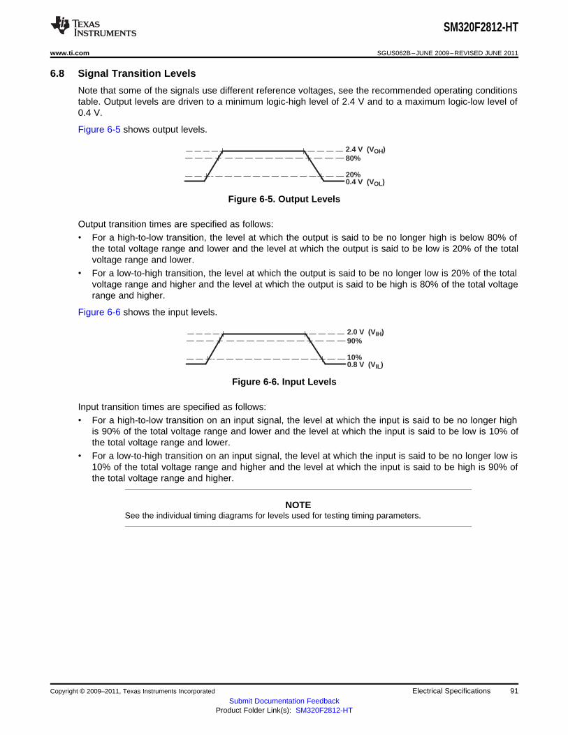
0.4 V (VOL)20%
2.4 V (VOH)80%
0.8 V (VIL)10%
2.0 V (VIH)90%
SM320F2812-HT
www.ti.com SGUS062B–JUNE 2009–REVISED JUNE 2011
6.8 Signal Transition Levels
Note that some of the signals use different reference voltages, see the recommended operating conditionstable. Output levels are driven to a minimum logic-high level of 2.4 V and to a maximum logic-low level of0.4 V.
Figure 6-5 shows output levels.
Figure 6-5. Output Levels
Output transition times are specified as follows:• For a high-to-low transition, the level at which the output is said to be no longer high is below 80% of
the total voltage range and lower and the level at which the output is said to be low is 20% of the totalvoltage range and lower.
• For a low-to-high transition, the level at which the output is said to be no longer low is 20% of the totalvoltage range and higher and the level at which the output is said to be high is 80% of the total voltagerange and higher.
Figure 6-6 shows the input levels.
Figure 6-6. Input Levels
Input transition times are specified as follows:• For a high-to-low transition on an input signal, the level at which the input is said to be no longer high
is 90% of the total voltage range and lower and the level at which the input is said to be low is 10% ofthe total voltage range and lower.
• For a low-to-high transition on an input signal, the level at which the input is said to be no longer low is10% of the total voltage range and higher and the level at which the input is said to be high is 90% ofthe total voltage range and higher.
NOTESee the individual timing diagrams for levels used for testing timing parameters.
Copyright © 2009–2011, Texas Instruments Incorporated Electrical Specifications 91Submit Documentation Feedback
Product Folder Link(s): SM320F2812-HT

Transmission Line
4.0 pF 1.85 pF
Z0 = 50 Ω(see note)
Tester Pin Electronics Data Sheet Timing Reference Point
OutputUnderTest
NOTE: The data sheet provides timing at the device pin. For output timing analysis, the tester pin electronics and its transmission line effects mustbe taken into account. A transmission line with a delay of 2 ns or longer can be used to produce the desired transmission line effect. Thetransmission line is intended as a load only. It is not necessary to add or subtract the transmission line delay (2 ns or longer) from the datasheet timing.
42 Ω 3.5 nH
Device Pin(see note)
Input requirements in this data sheet are tested with an input slew rate of < 4 Volts per nanosecond (4 V/ns) at the device pin.
SM320F2812-HT
SGUS062B–JUNE 2009–REVISED JUNE 2011 www.ti.com
6.9 Timing Parameter Symbology
Timing parameter symbols used are created in accordance with JEDEC Standard 100. To shorten thesymbols, some of the pin names and other related terminology have been abbreviated as follows:
Lowercase subscripts and their meanings: Letters and symbols and their meanings:
a access time H High
c cycle time (period) L Low
d delay time V Valid
f fall time X Unknown, changing, or don’t care level
h hold time Z High impedance
r rise time
su setup time
t transition time
v valid time
w pulse duration (width)
6.10 General Notes on Timing Parameters
All output signals from the 28x devices (including XCLKOUT) are derived from an internal clock such thatall output transitions for a given half-cycle occur with a minimum of skewing relative to each other.
The signal combinations shown in the following timing diagrams may not necessarily represent actualcycles. For actual cycle examples, see the appropriate cycle description section of this document.
6.11 Test Load Circuit
This test load circuit is used to measure all switching characteristics provided in this document.
Figure 6-7. 3.3-V Test Load Circuit
92 Electrical Specifications Copyright © 2009–2011, Texas Instruments Incorporated
Submit Documentation FeedbackProduct Folder Link(s): SM320F2812-HT

SM320F2812-HT
www.ti.com SGUS062B–JUNE 2009–REVISED JUNE 2011
6.12 Device Clock Table
This section provides the timing requirements and switching characteristics for the various clock optionsavailable on the F2812 DSP. Table 6-3 lists the cycle times of various clocks.
Table 6-3. Clock Table and Nomenclature
MIN NOM MAX UNIT
tc(OSC), Cycle time 28.6 50 nsOn-chip oscillator clock
Frequency 20 35 MHz
tc(CI), Cycle time 6.67 250 nsXCLKIN
Frequency 4 150 MHz
tc(SCO), Cycle time 6.67 500 nsSYSCLKOUT
Frequency 2 150 MHz
tc(XCO), Cycle time 6.67 2000 nsXCLKOUT
Frequency 0.5 150 MHz
tc(HCO), Cycle time 6.67 13.3 (1) nsHSPCLK
Frequency 75 (1) 150 MHz
tc(LCO), Cycle time 13.3 26.6 (1) nsLSPCLK
Frequency 37.5 (1) 75 MHz
tc(ADCCLK), Cycle time (2) 40 nsADC clock
Frequency 25 MHz
tc(SPC), Cycle time 50 nsSPI clock
Frequency 20 MHz
tc(CKG), Cycle time 50 nsMcBSP
Frequency 20 MHz
tc(XTIM), Cycle time 6.67 nsXTIMCLK
Frequency 150 MHz
(1) This is the default reset value if SYSCLKOUT = 150 MHz.(2) The maximum value for ADCCLK frequency is 25 MHz. For SYSCLKOUT values of 25 MHz or lower, ADCCLK has to be
SYSCLKOUT/2 or lower. ADCCLK = SYSCLKOUT is not a valid mode for any value of SYSCLKOUT.
6.13 Clock Requirements and Characteristics
6.13.1 Input Clock Requirements
The clock provided at the XCLKIN pin generates the internal CPU clock cycle.
Table 6-4. Input Clock Frequency (1)
PARAMETER MIN TYP MAX UNIT
Resonator (2) 20 35
fx Input clock frequency Crystal (2) 20 35 MHz
XCLKIN 4 150
fl Limp mode clock frequency 2 MHz
(1) Not production tested.(2) Not guaranteed for TA > 125°C.
Copyright © 2009–2011, Texas Instruments Incorporated Electrical Specifications 93Submit Documentation Feedback
Product Folder Link(s): SM320F2812-HT

SM320F2812-HT
SGUS062B–JUNE 2009–REVISED JUNE 2011 www.ti.com
Table 6-5. XCLKIN Timing Requirements – PLL Bypassed or Enabled (1)
NO. MIN MAX UNIT
C8 tc(CI) Cycle time, XCLKIN 6.67 250 ns
Up to 30 MHz 6C9 tf(CI) Fall time, XCLKIN ns
30 MHz to 150 MHz 2
Up to 30 MHz 6C10 tr(CI) Rise time, XCLKIN ns
30 MHz to 150 MHz 2
C11 tw(CIL) Pulse duration, X1/XCLKIN low as a percentage of tc(CI) 40 60 %
C12 tw(CIH) Pulse duration, X1/XCLKIN high as a percentage of tc(CI) 40 60 %
(1) Not production tested.
Table 6-6. XCLKIN Timing Requirements – PLL Disabled (1)
NO. MIN MAX UNIT
C8 tc(CI) Cycle time, XCLKIN 6.67 250 ns
Up to 30 MHz 6C9 tf(CI) Fall time, XCLKIN ns
30 MHz to 150 MHz 2
Up to 30 MHz 6C10 tr(CI) Rise time, XCLKIN ns
30 MHz to 150 MHz 2
XCLKIN ≤ 120 MHz 40 60C11 tw(CIL) Pulse duration, X1/XCLKIN low as a percentage of tc(CI) %
120 < XCLKIN ≤ 150 MHz 45 55
XCLKIN ≤ 120 MHz 40 60Pulse duration, X1/XCLKIN high as a percentage ofC12 tw(CIH) %tc(CI) 120 < XCLKIN ≤ 150 MHz 45 55
(1) Not production tested.
Table 6-7. Possible PLL Configuration Modes (1)
PLL MODE REMARKS SYSCLKOUT
Invoked by tying XPLLDIS pin low upon reset. PLL block is completely disabled. Clock input to thePLL Disabled XCLKINCPU (CLKIN) is directly derived from the clock signal present at the X1/XCLKIN pin.
Default PLL configuration upon power-up, if PLL is not disabled. The PLL itself is bypassed.PLL Bypassed However, the /2 module in the PLL block divides the clock input at the X1/XCLKIN pin by two before XCLKIN/2
feeding it to the CPU.
Achieved by writing a non-zero value n into PLLCR register. The /2 module in the PLL block nowPLL Enabled (XCLKIN × n)/2divides the output of the PLL by two before feeding it to the CPU.
(1) Not production tested.
6.13.2 Output Clock Characteristics
Table 6-8. XCLKOUT Switching Characteristics (PLL Bypassed or Enabled) (1) (2)
NO. PARAMETER MIN TYP MAX UNIT
C1 tc(XCO) Cycle time, XCLKOUT 6.67 (3) ns
C3 (4) tf(XCO) Fall time, XCLKOUT 2 ns
C4 (4) tr(XCO) Rise time, XCLKOUT 2 ns
C5 (4) tw(XCOL) Pulse duration, XCLKOUT low H–2 H+2 ns
C6 (4) tw(XCOH) Pulse duration, XCLKOUT high H–2 H+2 ns
C7 (4) tp PLL lock time (5) 131 072tc(CI) ns
(1) A load of 40 pF is assumed for these parameters.(2) H = 0.5tc(XCO)(3) The PLL must be used for maximum frequency operation.(4) Not production tested.(5) This parameter has changed from 4096 XCLKIN cycles in the earlier revisions of the silicon.
94 Electrical Specifications Copyright © 2009–2011, Texas Instruments Incorporated
Submit Documentation FeedbackProduct Folder Link(s): SM320F2812-HT

See Note A
See Note B
SM320F2812-HT
www.ti.com SGUS062B–JUNE 2009–REVISED JUNE 2011
A. The relationship of XCLKIN to XCLKOUT depends on the divide factor chosen. The waveform relationship shown inFigure 6-8 is intended to illustrate the timing parameters only and may differ based on configuration.
B. XCLKOUT configured to reflect SYSCLKOUT.
Figure 6-8. Clock Timing
6.14 Reset Timing
Table 6-9. Reset (XRS) Timing Requirements (1) (2)
MIN NOM MAX UNIT
tw(RSL1) Pulse duration, stable XCLKIN to XRS high 8tc(CI) cycles
tw(RSL2) Pulse duration, XRS low Warm reset 8tc(CI) cycles
WD-initiated reset 512tc(CI)
Pulse duration, reset pulse generated bytw(WDRS) 512tc(CI) cycleswatchdog
td(EX) Delay time, address/data valid after XRS high 32tc(CI) cycles
tOSCST(3) Oscillator start-up time 1 10 ms
tsu(XPLLDIS) Setup time for XPLLDIS pin 16tc(CI) cycles
th(XPLLDIS) Hold time for XPLLDIS pin 16tc(CI) cycles
th(XMP/MC) Hold time for XMP/MC pin 16tc(CI) cycles
th(boot-mode) Hold time for boot-mode pins 2520tc(CI)(4) cycles
(1) If external oscillator/clock source isused, reset time has to be low at least for 1 ms after VDD reaches 1.5 V.(2) Not production tested.(3) Dependent on crystal/resonator and board design.(4) The boot ROM reads the password locations. Therefore, this timing requirement includes the wakeup time for flash. See the
TMS320x281x Boot ROM Reference Guide (SPRU095) and TMS320x281x System Control and Interrupts Reference Guide (SPRU078)for further information.
Copyright © 2009–2011, Texas Instruments Incorporated Electrical Specifications 95Submit Documentation Feedback
Product Folder Link(s): SM320F2812-HT

tw(RSL1)
th(XPLLDIS)
th(XMP/MC)
th(boot-mode)(See Note D)
VDDIO, VDD3VFLVDDAn, VDDAIO
(3.3 V) (See Note B)
XCLKIN
2.5 V
0.3 V
X1
XRS
XF/XPLLDIS
XMP/MC
Boot-Mode Pins
VDD, VDD1(1.8 V (or 1.9 V))
XCLKOUT
I/O Pins
User-Code Dependent
User-Code Dependent
User-Code Dependent
Boot-ROM Execution StartsPeripheral/GPIO FunctionBased on Boot Code
GPIO Pins as Input
XPLLDIS Sampling
GPIOF14
XCLKIN/8 (See Note C)
GPIO Pins as Input (State Depends on Internal PU/PD)
tOSCST
(Don’t Care)
(Don’t Care)
User-Code Dependent
Address/Data/Control
Address/Data V alid. Internal Boot-ROM Code Execution Phase
User-Code Execution Phase
NOTES: A. The state of the GPIO pins is undefined (i.e., they could be input or output) until the 1.8-V (or 1.9-V) supply reaches at least 1 Vand 3.3-V supply reaches 2.5 V.
B. VDDAn − VDDA1/VDDA2 and AVDDREFBGC. Upon power up, SYSCLKOUT is XCLKIN/2 if the PLL is enabled. Since both the XTIMCLK and CLKMODE bits in the XINTCNF2
register come up with a reset state of 1, SYSCLKOUT is further divided by 4 before it appears at XCLKOUT. This explains whyXCLKOUT = XCLKIN/8 during this phase.
D. After reset, the Boot ROM code executes instructions for 1260 SYSCLKOUT cycles (SYSCLKOUT = XCLKIN/2) and thensamples BOOT Mode pins. Based on the status of the Boot Mode pin, the boot code branches to destination memory or bootcode function in ROM. The BOOT Mode pins should be held high/low for at least 2520 XCLKIN cycles from boot ROM executiontime for proper selection of Boot modes.If Boot ROM code executes after power-on conditions (in debugger environment), the Boot code execution time is based onthe current SYSCLKOUT speed. The SYSCLKOUT is based on user environment and could be with or without PLL enabled.
td(EX)
See Note A
tsu(XPLLDIS)
SM320F2812-HT
SGUS062B–JUNE 2009–REVISED JUNE 2011 www.ti.com
Figure 6-9. Power-on Reset in Microcomputer Mode (XMP/MC = 0) (See Note A)
96 Electrical Specifications Copyright © 2009–2011, Texas Instruments Incorporated
Submit Documentation FeedbackProduct Folder Link(s): SM320F2812-HT
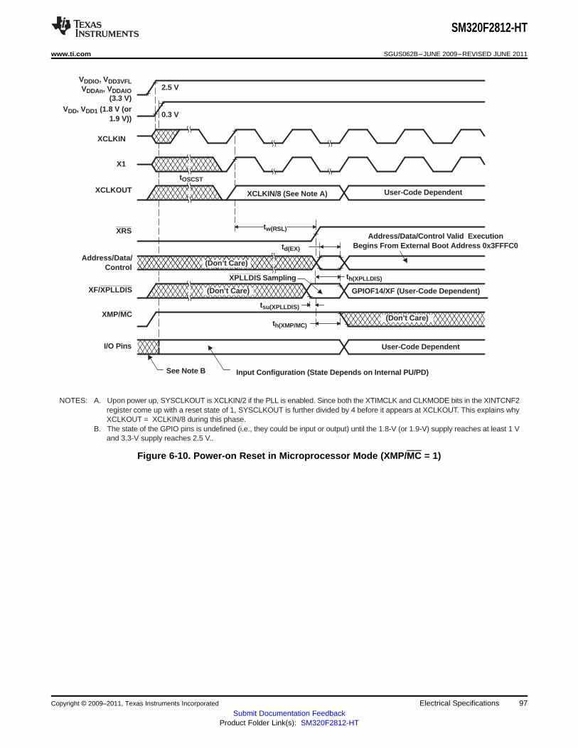
tw(RSL)
th(XPLLDIS)
th(XMP/MC)
tOSCST
VDDIO, VDD3VFLVDDAn, VDDAIO
(3.3 V)
XCLKIN
X1
XRS
XF/XPLLDIS
XMP/MC
VDD, VDD1 (1.8 V (or1.9 V))
I/O Pins
XPLLDIS Sampling
Address/Data/Control
XCLKOUT
(Don’t Care)
(Don’t Care)
GPIOF14/XF (User-Code Dependent)
XCLKIN/8 (See Note A)
(Don’t Care)
Input Configuration (State Depends on Internal PU/PD)
User-Code Dependent
Address/Data/Control V alid ExecutionBegins From External Boot Address 0x3FFFC0
User-Code Dependent
2.5 V
0.3 V
td(EX)
NOTES: A. Upon power up, SYSCLKOUT is XCLKIN/2 if the PLL is enabled. Since both the XTIMCLK and CLKMODE bits in the XINTCNF2register come up with a reset state of 1, SYSCLKOUT is further divided by 4 before it appears at XCLKOUT. This explains whyXCLKOUT = XCLKIN/8 during this phase.
B. The state of the GPIO pins is undefined (i.e., they could be input or output) until the 1.8-V (or 1.9-V) supply reaches at least 1 Vand 3.3-V supply reaches 2.5 V..
See Note B
tsu(XPLLDIS)
SM320F2812-HT
www.ti.com SGUS062B–JUNE 2009–REVISED JUNE 2011
Figure 6-10. Power-on Reset in Microprocessor Mode (XMP/MC = 1)
Copyright © 2009–2011, Texas Instruments Incorporated Electrical Specifications 97Submit Documentation Feedback
Product Folder Link(s): SM320F2812-HT
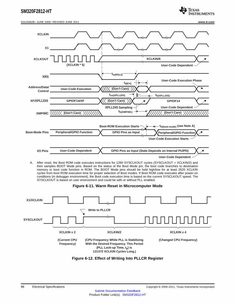
XCLKIN/8
(XCLKIN * 5)
th(XPLLDIS)
th(XMP/MC)
th(boot-mode) (see Note A)
tw(RSL2)
XCLKIN
X1
XRS
XF/XPLLDIS
XMP/MC
Boot-Mode Pins
XCLKOUT
I/O Pins
Address/Data/Control
Boot-ROM Execution Starts
User-Code Execution Starts
User-Code Dependent
User-Code Dependent
User-Code Execution Phase
(Don’t Care)
(Don’t Care)
(Don’t Care)(Don’t Care)
User-Code Dependent
User-Code Execution
Peripheral/GPIO Function
User-Code Dependent
GPIO Pins as Input (State Depends on Internal PU/PD)
GPIO Pins as Input
GPIOF14/XF
XPLLDIS Sampling
GPIOF14
Peripheral/GPIO Function
td(EX)
tsu(XPLLDIS)
X1/XCLKIN
SYSCLKOUT
Write to PLLCR
XCLKIN x 2
(Current CPUFrequency)
XCLKIN/2
(CPU Frequency While PLL is StabilizingWith the Desired Frequency . This Period
(PLL Lock-up T ime, t p) is131072 XCLKIN Cycles Long.)
XCLKIN x 4
(Changed CPU Frequency)
SM320F2812-HT
SGUS062B–JUNE 2009–REVISED JUNE 2011 www.ti.com
A. After reset, the Boot ROM code executes instructions for 1260 SYSCLKOUT cycles (SYSCLKOUT = XCLKIN/2) andthen samples BOOT Mode pins. Based on the status of the Boot Mode pin, the boot code branches to destinationmemory or boot code function in ROM. The BOOT Mode pins should be held high/low for at least 2520 XCLKINcycles from boot ROM execution time for proper selection of Boot modes. If Boot ROM code executes after power-onconditions (in debugger environment), the Boot code execution time is based on the current SYSCLKOUT speed. TheSYSCLKOUT is based on user environment and could be with or without PLL enabled.
Figure 6-11. Warm Reset in Microcomputer Mode
Figure 6-12. Effect of Writing Into PLLCR Register
98 Electrical Specifications Copyright © 2009–2011, Texas Instruments Incorporated
Submit Documentation FeedbackProduct Folder Link(s): SM320F2812-HT

WAKE INT(see Note B)
XCLKOUT(see Note A)
A0−A15
td(WAKE−IDLE)
tw(WAKE−INT)
SM320F2812-HT
www.ti.com SGUS062B–JUNE 2009–REVISED JUNE 2011
6.15 Low-Power Mode Wakeup Timing
Table 6-10 is also the IDLE Mode Wake-Up Timing Requirements table.
Table 6-10. IDLE Mode Switching Characteristics (1)
PARAMETER TEST CONDITIONS MIN TYP MAX UNIT
Without input qualifier 2 x tc(SCO) CyclesPulse duration, external wake-uptw(WAKE-INT) signal With input qualifier 1 × tc(SCO) + IQT (2) Cycles
Delay time, external wake signalto program execution resume (3)
–Wake-up from Flash Without input qualifier 8 × tc(SCO) Cycles–Flash module in active state
– Wake-up from Flash With input qualifier 8 × tc(SCO) + IQT (2) Cycles–Flash module in active statetd(WAKE-IDLE) –Wake-up from Flash Without input qualifier 1050 × tc(SCO) Cycles–Flash module in sleep state
–Wake-up from Flash With input qualifier 1050 × tc(SCO) + IQT (2) Cycles–Flash module in sleep state
–Wake-up from SARAM Without input qualifier 8 × tc(SCO) Cycles
–Wake-up from SARAM With input qualifier 8 × tc(SCO) + IQT (2) Cycles
(1) Not production tested.(2) Input Qualification Time (IQT) = [5 × QUALPRD × 2] × tc(SCO)(3) This is the time taken to begin execution of the instruction that immediately follows the IDLE instruction. Execution of an ISR (triggered
by the wake-up) signal involves additional latency.
A. XCLKOUT = SYSCLKOUTB. WAKE INT can be any enabled interrupt, WDINT, XNMI, or XRS.
Figure 6-13. IDLE Entry and Exit Timing
Copyright © 2009–2011, Texas Instruments Incorporated Electrical Specifications 99Submit Documentation Feedback
Product Folder Link(s): SM320F2812-HT

SM320F2812-HT
SGUS062B–JUNE 2009–REVISED JUNE 2011 www.ti.com
Table 6-11 is also the STANDBY Mode Wake-Up Timing Requirements table.
Table 6-11. STANDBY Mode Switching Characteristics (1)
PARAMETER TEST CONDITIONS MIN TYP MAX UNIT
Delay time, IDLE instructiontd(IDLE-XCOH) 32 × tc(SCO) 12 × tc(CI) Cyclesexecuted to XCLKOUT high
Without input 12 × tc(CI) CyclesPulse duration, external qualifiertw(WAKE-INT) wake-up signalWith input qualifier (2 + QUALSTDBY) (2) × tc(CI) Cycles
Delay time, external wakesignal to program executionresume (3)
–Wake-up from Flash Without input–Flash module in active 12 × tc(CI) Cyclesqualifierstate
–Wake-up from Flash–Flash module in active With input qualifier 12 × tc(CI) + tw(WAKE-INT) Cyclesstate
td(WAKE-STBY) –Wake-up from Flash Without input–Flash module in sleep 1125 × tc(SCO) Cyclesqualifierstate
–Wake-up from Flash–Flash module in sleep With input qualifier 1125 × tc(SCO) + tw(WAKE-INT) Cyclesstate
Without input–Wake-up from SARAM 12 x tc(CI) Cyclesqualifier
–Wake-up from SARAM With input qualifier 12 × tc(CI) + tw(WAKE-INT) Cycles
(1) Not production tested.(2) QUALSTDBY is a 6-bit field in the LPMCR0 register.(3) This is the time taken to begin execution of the instruction that immediately follows the IDLE instruction. Execution of an ISR (triggered
by the wake-up) signal involves additional latency.
100 Electrical Specifications Copyright © 2009–2011, Texas Instruments Incorporated
Submit Documentation FeedbackProduct Folder Link(s): SM320F2812-HT

tw(WAKE-INT)
td(WAKE-STBY)
td(IDLE−XCOH)
32 SYSCLKOUT Cycles
Wake−upSignal
X1/XCLKIN
XCLKOUT†
STANDBY Normal ExecutionSTANDBY
Flushing Pipeline
AB
CD
EF
DeviceStatus
NOTES: A. IDLE instruction is executed to put the device into STANDBY mode.B. The PLL block responds to the STANDBY signal. SYSCLKOUT is held for approximately 32 cycles before being turned
off. This 32-cycle delay enables the CPU pipe and any other pending operations to flush properly.C. The device is now in STANDBY mode.D. The external wake-up signal is driven active (negative edge triggered shown as an example).E. After a latency period, the STANDBY mode is exited.F. Normal operation resumes. The device responds to the interrupt (if enabled).
SM320F2812-HT
www.ti.com SGUS062B–JUNE 2009–REVISED JUNE 2011
Figure 6-14. STANDBY Entry and Exit Timing
Copyright © 2009–2011, Texas Instruments Incorporated Electrical Specifications 101Submit Documentation Feedback
Product Folder Link(s): SM320F2812-HT
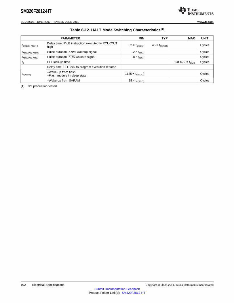
SM320F2812-HT
SGUS062B–JUNE 2009–REVISED JUNE 2011 www.ti.com
Table 6-12. HALT Mode Switching Characteristics (1)
PARAMETER MIN TYP MAX UNIT
Delay time, IDLE instruction executed to XCLKOUTtd(IDLE-XCOH) 32 × tc(SCO) 45 × tc(SCO) Cycleshigh
tw(WAKE-XNMI) Pulse duration, XNMI wakeup signal 2 × tc(CI) Cycles
tw(WAKE-XRS) Pulse duration, XRS wakeup signal 8 × tc(CI) Cycles
tp PLL lock-up time 131 072 × tc(CI) Cycles
Delay time, PLL lock to program execution resume
–Wake-up from flashtd(wake) 1125 × tc(SCO) Cycles–Flash module in sleep state
–Wake-up from SARAM 35 × tc(SCO) Cycles
(1) Not production tested.
102 Electrical Specifications Copyright © 2009–2011, Texas Instruments Incorporated
Submit Documentation FeedbackProduct Folder Link(s): SM320F2812-HT

SM320F2812-HT
www.ti.com SGUS062B–JUNE 2009–REVISED JUNE 2011
A. IDLE instruction is executed to put the device into HALT mode.B. The PLL block responds to the HALT signal. SYSCLKOUT is held for another 32 cycles before the oscillator is turned
off and the CLKIN to the core is stopped. This 32-cycle delay enables the CPU pipe and any other pendingoperations to flush perperly.
C. Clocks to the device are turned off and the internal oscillator and PLL are shut down. The device is now in HALTmode and consumes absolute minimum power.
D. When XNMI is friven active (negative edge triggered shown, as an example), the oscillator is turned on; but the PLL isnot activiated.
E. When XNMI is deactiveted, it initiates the PLL lock sequence, which takes 131, 072 X1/XCLKIN cycles.F. When CLKIN to the core is enabled, the device responds to the interrupt (if enabled), after a latency. The HALT mode
is now exited.G. Normal operation resumes.H. XCLKOUT = SYSCLKOUT
Figure 6-15. HALT Wakeup Using XNMI
6.16 Event Manager Interface
6.16.1 PWM Timing
PWM refers to all PWM outputs on EVA and EVB.
Copyright © 2009–2011, Texas Instruments Incorporated Electrical Specifications 103Submit Documentation Feedback
Product Folder Link(s): SM320F2812-HT

tw(PWM)
td(PWM)XCO
PWMx
XCLKOUT
(see Note A)
XCLKOUT
(see Note A)
tw(TDIR)
TDIRx
SM320F2812-HT
SGUS062B–JUNE 2009–REVISED JUNE 2011 www.ti.com
Table 6-13. PWM Switching Characteristics (1) (2)
PARAMETER TEST CONDITIONS MIN MAX UNIT
tw(PWM)(3) (4) Pulse duration, PWMx output high/low 25 ns
td(PWM)XCO Delay time, XCLKOUT high to PWMx output switching XCLKOUT = SYSCLKOUT/4 10 ns
(1) See the GPIO output timing for fall/rise times for PWM pins.(2) PWM pin toggling frequency is limited by the GPIO output buffer switching frequency (20 MHz).(3) PWM outputs may be 100%, 0%, or increments of tc(HCO) with respect to the PWM period.(4) Not production tested.
Table 6-14. Timer and Capture Unit Timing Requirements (1) (2) (3)
MIN MAX UNIT
Without input qualifier 2 × tc(SCO)tw(TDIR) Pulse duration, TDIRx low/high cycles
With input qualifier 1 × tc(SCO) + IQT (4)
Without input qualifier 2 × tc(SCO)tw(CAP) Pulse duration, CAPx input low/high cycles
With input qualifier 1 x tc(SCO) + IQT (4)
tw(TCLKINL) Pulse duration, TCLKINx low as a percentage of TCLKINx cycle time 40 60 %
tw(TCLKINH) Pulse duration, TCLKINx high as a percentage of TCLKINx cycle time 40 60 %
tc(TCLKIN) Cycle time, TCLKINx 4 × tc(HCO) ns
(1) The QUALPRD bit field value can range from 0 (no qualification) through 0xFF (510 SYSCLKOUT cycles). The qualification samplingperiod is 2n SYSCLKOUT cycles, where n is the value stored in the QUALPRD bit field. As an example, when QUALPRD = 1, thequalification sampling period is 1 × 2 = 2 SYSCLKOUT cycles (i.e., the input is sampled every 2 SYSCLKOUT cycles). Six such samplesare taken over five sampling windows, each window being 2n SYSCLKOUT cycles. For QUALPRD = 1, the minimum width that isneeded is 5 × 2 = 10 SYSCLKOUT cycles. However, since the external signal is driven asynchronously, a 11-SYSCLKOUT-wide pulseensures reliable recognition.
(2) Maximum input frequency to the QEP = min[HSPCLK/2, 20 MHz](3) Not production tested.(4) Input Qualification Time (IQT) = [5 × QUALPRD × 2] × tc(SCO)
A. XCLKOUT = SYSCLKOUT
Figure 6-16. PWM Output Timing
A. XCLKOUT = SYSCLKOUT
Figure 6-17. TDIRx Timing
104 Electrical Specifications Copyright © 2009–2011, Texas Instruments Incorporated
Submit Documentation FeedbackProduct Folder Link(s): SM320F2812-HT

XCLKOUT
td(XCOH-EVASOCL)
EVASOC
tw(EVASOCL)
XCLKOUT
td(XCOH-EVBSOCL)
EVBSOC
tw(EVBSOCL)
SM320F2812-HT
www.ti.com SGUS062B–JUNE 2009–REVISED JUNE 2011
Table 6-15. External ADC Start-of-Conversion – EVA – Switching Characteristics (1) (2)
PARAMETER MIN MAX UNIT
td(XCOH-EVASOCL) Delay time, XCLKOUT high to EVASOC low 1 × tc(SCO) cycle
tw(EVASOCL) Pulse duration, EVASOC low 32 × tc(HCO) ns
(1) XCLKOUT = SYSCLKOUT(2) Not production tested.
Figure 6-18. EVASOC Timing
Table 6-16. External ADC Start-of-Conversion – EVB – Switching Characteristics (1) (2)
PARAMETER MIN MAX UNIT
td(XCOH-EVBSOCL) Delay time, XCLKOUT high to EVBSOC low 1 × tc(SCO) cycle
tw(EVBSOCL) Pulse duration, EVBSOC low 32 × tc(HCO) ns
(1) XCLKOUT = SYSCLKOUT(2) Not production tested.
Figure 6-19. EVBSOC Timing
6.16.2 Interrupt Timing
Table 6-17. Interrupt Switching Characteristics
PARAMETER MIN MAX UNIT
Without input 12qualifierDelay time, PDPINTx low to PWMtd(PDP-PWM)HZ nshigh-impedance state 1 × tc(SCO) + IQT +With input qualifier 12 (1)
Without input 3 × tc(SCO)Delay time, CxTRIP/TxCTRIP signals low qualifiertd(TRIP-PWM)HZ(2) nsto PWM high-impedance state
With input qualifier [2 × tc(SCO)] + IQT(1)
Delay time, INT low/high totd(INT)(2) tqual + 12tc(XCO) nsinterrupt-vector fetch
(1) Input Qualification Time (IQT) = [5 × QUALPRD × 2] × tc(SCO)(2) Not production tested.
Copyright © 2009–2011, Texas Instruments Incorporated Electrical Specifications 105Submit Documentation Feedback
Product Folder Link(s): SM320F2812-HT

PWM(see Note C)
TxCTRIP, CxTRIP,PDPINTx
(see Note B)
XCLKOUT(see Note A)
tw(PDP), tw(CxTRIP) , tw(TxCTRIP)
td(PDP-PWM)HZ , td(TRIP-PWM)HZ
XNMI, XINT1, XINT2
tw(INT)
Interrupt V ector
td(INT)
A0−A15
SM320F2812-HT
SGUS062B–JUNE 2009–REVISED JUNE 2011 www.ti.com
Table 6-18. Interrupt Timing Requirements
MIN MAX UNIT
with no qualifier 2 × tc(SCO)tw(INT)
(1) Pulse duration, INT input low/high cycleswith qualifier 1 × tc(SCO) + IQT (2)
with no qualifier 2 × tc(SCO)tw(PDP) Pulse duration, PDPINTx input low cycles
with qualifier 1 × tc(SCO) + IQT (2)
with no qualifier 2 × tc(SCO)tw(CxTRIP)
(1) Pulse duration, CxTRIP input low cycleswith qualifier 1 × tc(SCO) + IQT (2)
with no qualifier 2 × tc(SCO)tw(TxCTRIP)
(1) Pulse duration, TxCTRIP input low cycleswith qualifier 1 × tc(SCO) + IQT (2)
(1) Not production tested.(2) Input Qualification Time (IQT) = [5 × QUALPRD × 2] × tc(SCO)
A. XCLKOUT = SYSCLKOUTB. TxCTRIP – T1CTRIP, T2CTRIP, T3CTRIP, T4CTRIP . CxTRIP – C1TRIP, C2TRIP, C3TRIP, C4TRIP, C5TRIP, or
C6TRIP. PDPINTx – PDPINTA or PDPINTBC. PWM refers to all the PWM pins in the device (i.e., PWMn and TnPWM pins or PWM pin pair relevant to each
CxTRIP pin). The state of the PWM pins after PDPINTx is taken high depends on the state of the FCOMPOE bit.
Figure 6-20. External Interrupt Timing
6.17 General-Purpose Input/Output (GPIO) – Output Timing
Table 6-19. General-Purpose Output Switching Characteristics
PARAMETER MIN MAX UNIT
td(XCOH-GPO) Delay time, XCLKOUT high to GPIO low/high All GPIOs 1 × tc(SCO) cycle
tr(GPO)(1) Rise time, GPIO switching low to high All GPIOs 10 ns
tf(GPO)(1) Fall time, GPIO switching high to low All GPIOs 10 ns
fGPO(1) Toggling frequency, GPO pins 20 MHz
(1) Not production tested.
106 Electrical Specifications Copyright © 2009–2011, Texas Instruments Incorporated
Submit Documentation FeedbackProduct Folder Link(s): SM320F2812-HT

td(XCOH-GPO)
GPIO
XCLKOUT
tr(GPO)tf(GPO)
GPIOSignal
1
Sampling Window QUALPRD
Output FromQualifier
1 1 1 1 1 1 1 1 1 1 10 0 0 0 0 0 0 0 0 0
SYSCLKOUT
QUALPRD = 1 (2 x SYSCLKOUT cycles) x 5
NOTES: A. This glitch is ignored by the input qualifier. The QUALPRD bit field specifies the qualification sampling period. It can vary from 00to 0xFF. Input qualification is not applicable when QUALPRD = 00. For any other value n, the qualification sampling period in 2nSYSCLKOUT cycles (i.e., at every 2n SYSCLKOUT cycle, the GPIO pin is sampled). Six consecutive samples must be of thesame value for a given input to be recognized.
B. For the qualifier to detect the change, the input should be stable for 10 SYSCLKOUT cycles or greater. In other words, the inputsshould be stable for (5 x QUALPRD x 2) SYSCLKOUT cycles. This would ensure six sampling windows for detection to occur.Since external signals are driven asynchronously, an 11-SYSCLKOUT-wide pulse ensures reliable recognition.
See Note A
SM320F2812-HT
www.ti.com SGUS062B–JUNE 2009–REVISED JUNE 2011
Figure 6-21. General-Purpose Output Timing
6.18 General-Purpose Input/Output (GPIO) – Input Timing
Figure 6-22. GPIO Input Qualifier – Example Diagram for QUALPRD = 1
Table 6-20. General-Purpose Input Timing Requirements (1)
MIN MAX UNIT
With no qualifier 2 × tc(SCO)tw(GPI) Pulse duration, GPIO low/high All GPIOs cycles
With qualifier 1 × tc(SCO) + IQT (2)
(1) Not production tested.(2) Input Qualification Time (IQT) = [5 × QUALPRD × 2] × tc(SCO)
Copyright © 2009–2011, Texas Instruments Incorporated Electrical Specifications 107Submit Documentation Feedback
Product Folder Link(s): SM320F2812-HT

tc(SPC) SPI clock cycle time LSPCLK
4or LSPCLK
(SPIBRR 1) tc(LCO) LSPCLK cycle time
GPIOxn
XCLKOUT
tw(GPI)
(2)
SM320F2812-HT
SGUS062B–JUNE 2009–REVISED JUNE 2011 www.ti.com
Figure 6-23. General-Purpose Input Timing
NOTEThe pulse width requirement for general-purpose input is applicable for the XBIO andADCSOC pins as well.
6.19 SPI Master Mode Timing
Table 6-21. SPI Master Mode External Timing (Clock Phase = 0) (1) (2) (3)
SPI WHEN (SPIBRR + 1) SPI WHEN (SPIBRR + 1)IS EVEN OR IS ODD AND
NO. UNITSPIBRR = 0 OR 2 SPIBRR > 3
MIN MAX MIN MAX
1 tc(SPC)M Cycle time, SPICLK 4tc(LCO) 128tc(LCO) 5tc(LCO) 127tc(LCO) ns
Pulse duration, SPICLK hightw(SPCH)M 0.5tc(SPC)M – 10 0.5tc(SPC)M 0.5tc(SPC)M – 0.5tc(LCO) – 10 0.5tc(SPC)M – 0.5tc(LCO)(clock polarity = 0)
2 (4) nsPulse duration, SPICLK low
tw(SPCL)M 0.5tc(SPC)M – 10 0.5tc(SPC)M 0.5tc(SPC)M – 0.5tc(LCO) – 10 0.5tc(SPC)M – 0.5tc(LCO)(clock polarity = 1)
Pulse duration, SPICLK lowtw(SPCL)M 0.5tc(SPC)M – 10 0.5tc(SPC)M 0.5tc(SPC)M + 0.5tc(LCO) – 10 0.5tc(SPC)M + 0.5tc(LCO)(clock polarity = 0)
3(4) nsPulse duration, SPICLK high
tw(SPCH)M 0.5tc(SPC)M – 10 0.5tc(SPC)M 0.5tc(SPC)M + 0.5tc(LCO) – 10 0.5tc(SPC)M + 0.5tc(LCO)(clock polarity = 1)
Delay time, SPICLK high to SPISIMOtd(SPCH-SIMO)M –10 10 –10 10
valid (clock polarity = 0)4(4) ns
Delay time, SPICLK low to SPISIMOtd(SPCL-SIMO)M –10 10 –10 10
valid (clock polarity = 1)
Valid time, SPISIMO data valid aftertv(SPCL-SIMO)M 0.5tc(SPC)M – 10 0.5tc(SPC)M + 0.5tc(LCO) – 10
SPICLK low (clock polarity = 0)5(4) ns
Valid time, SPISIMO data valid aftertv(SPCH-SIMO)M 0.5tc(SPC)M – 10 0.5tc(SPC)M + 0.5tc(LCO) – 10
SPICLK high (clock polarity = 1)
Setup time, SPISOMI before SPICLKtsu(SOMI-SPCL)M 0 0
low (clock polarity = 0)8(4) ns
Setup time, SPISOMI before SPICLKtsu(SOMI-SPCH)M 0 0
high (clock polarity = 1)
Valid time, SPISOMI data valid aftertv(SPCL-SOMI)M 0.25tc(SPC)M – 10 0.5tc(SPC)M – 0.5tc(LCO) – 10
SPICLK low (clock polarity = 0)9(4) ns
Valid time, SPISOMI data valid aftertv(SPCH-SOMI)M 0.25tc(SPC)M – 10 0.5tc(SPC)M – 0.5tc(LCO) – 10
SPICLK high (clock polarity = 1)
(1) The MASTER/SLAVE bit (SPICTL.2) is set and the CLOCK PHASE bit (SPICTL.3) is cleared.
(3) Not production tested.(4) The active edge of the SPICLK signal referenced is controlled by the CLOCK POLARITY bit (SPICCR.6).
108 Electrical Specifications Copyright © 2009–2011, Texas Instruments Incorporated
Submit Documentation FeedbackProduct Folder Link(s): SM320F2812-HT

9
4
SPISOMI
SPISIMO
SPICLK (clock polarity = 1)
SPICLK (clock polarity = 0)
Master In DataMust Be Valid
Master Out Data Is Valid
8
5
3
2
1
SPISTE(see Note A)
SM320F2812-HT
www.ti.com SGUS062B–JUNE 2009–REVISED JUNE 2011
NOTEInternal clock prescalers must be adjusted such that the SPI clock speed is not greater thanthe I/O buffer speed limit (20 MHz).
A. In the master mode, SPISTE goes active 0.5tc(SPC) before valid SPI clock edge. On the trailing end of the word, theSPISTE will go inactive 0.5tc(SPC) after the receiving edge (SPICLK) of the last data bit.
Figure 6-24. SPI Master Mode External Timing (Clock Phase = 0)
Copyright © 2009–2011, Texas Instruments Incorporated Electrical Specifications 109Submit Documentation Feedback
Product Folder Link(s): SM320F2812-HT

tc(SPC) SPI clock cycle time LSPCLK
4or LSPCLK
(SPIBRR 1) tc(LCO) LSPCLK cycle time
(2)
SM320F2812-HT
SGUS062B–JUNE 2009–REVISED JUNE 2011 www.ti.com
Table 6-22. SPI Master Mode External Timing (Clock Phase = 1) (1) (2) (3)
SPI WHEN (SPIBRR + 1) SPI WHEN (SPIBRR + 1)IS EVEN OR IS ODD AND
NO. UNITSPIBRR = 0 OR 2 SPIBRR > 3
MIN MAX MIN MAX
1 tc(SPC)M Cycle time, SPICLK 4tc(LCO) 128tc(LCO) 5tc(LCO) 127tc(LCO) ns
Pulse duration, SPICLK hightw(SPCH)M 0.5tc(SPC)M – 10 0.5tc(SPC)M 0.5tc(SPC)M – 0.5tc (LCO) – 10 0.5tc(SPC)M – 0.5tc(LCO)(clock polarity = 0)
2 (4) nsPulse duration, SPICLK low
tw(SPCL)M 0.5tc(SPC)M – 10 0.5tc(SPC)M 0.5tc(SPC)M – 0.5tc (LCO) – 10 0.5tc(SPC)M – 0.5tc(LCO)(clock polarity = 1)
Pulse duration, SPICLK lowtw(SPCL)M 0.5tc(SPC)M – 10 0.5tc(SPC)M 0.5tc(SPC)M + 0.5tc(LCO) – 10 0.5tc(SPC)M – 0.5tc(LCO)(clock polarity = 0)
3(4) nsPulse duration, SPICLK high
tw(SPCH)M 0.5tc(SPC)M – 10 0.5tc(SPC)M 0.5tc(SPC)M + 0.5tc(LCO) – 10 0.5tc(SPC)M – 0.5tc(LCO)(clock polarity = 1)
Setup time, SPISIMO data validtsu(SIMO-SPCH)M before SPICLK high (clock 0.5tc(SPC)M – 10 0.5tc(SPC)M – 10
polarity = 0)6(4) ns
Setup time, SPISIMO data validtsu(SIMO-SPCL)M before SPICLK low (clock 0.5tc(SPC)M – 10 0.5tc(SPC)M – 10
polarity = 1)
Valid time, SPISIMO data validtv(SPCH-SIMO)M after SPICLK high (clock polarity 0.5tc(SPC)M – 10 0.5tc(SPC)M – 10
= 0)7(4) ns
Valid time, SPISIMO data validtv(SPCL-SIMO)M after SPICLK low (clock polarity 0.5tc(SPC)M – 10 0.5tc(SPC)M – 10
= 1)
Setup time, SPISOMI beforetsu(SOMI-SPCH)M SPICLK high 0 0
(clock polarity = 0)10(4) ns
Setup time, SPISOMI beforetsu(SOMI-SPCL)M SPICLK low 0 0
(clock polarity = 1)
Valid time, SPISOMI data validtv(SPCH-SOMI)M after SPICLK high (clock polarity 0.25tc(SPC)M – 10 0.5tc(SPC)M – 10
= 0)11(4) ns
Valid time, SPISOMI data validtv(SPCL-SOMI)M after SPICLK low (clock polarity 0.25tc(SPC)M – 10 0.5tc(SPC)M – 10
= 1)
(1) The MASTER/SLAVE bit (SPICTL.2) is set and the CLOCK PHASE bit (SPICTL.3) is set.
(3) Not production tested..(4) The active edge of the SPICLK signal referenced is controlled by the CLOCK POLARITY bit (SPICCR.6).
110 Electrical Specifications Copyright © 2009–2011, Texas Instruments Incorporated
Submit Documentation FeedbackProduct Folder Link(s): SM320F2812-HT

Data Valid
11
SPISOMI
SPISIMO
SPICLK (clock polarity = 1)
SPICLK (clock polarity = 0)
Master In DataMust Be Valid
Master Out Data Is Valid
1
7
6
10
3
2
SPISTE(see Note A)
SM320F2812-HT
www.ti.com SGUS062B–JUNE 2009–REVISED JUNE 2011
A. In the master mode, SPISTE goes active 0.5tc(SPC) before valid SPI clock edge. On the trailing end of the word, theSPISTE will go inactive 0.5tc(SPC) after the receiving edge (SPICLK) of the last data bit.
Figure 6-25. SPI Master External Timing (Clock Phase = 1)
Copyright © 2009–2011, Texas Instruments Incorporated Electrical Specifications 111Submit Documentation Feedback
Product Folder Link(s): SM320F2812-HT

tc(SPC) SPI clock cycle time LSPCLK
4or LSPCLK
(SPIBRR 1) tc(LCO) LSPCLK cycle time
20
15
SPISIMO
SPISOMI
SPICLK(clock polarity = 1)
SPICLK(clock polarity = 0)
SPISIMO DataMust Be Valid
SPISOMI Data Is Valid
19
16
14
13
12
SPISTE(see Note A)
(2)
SM320F2812-HT
SGUS062B–JUNE 2009–REVISED JUNE 2011 www.ti.com
6.20 SPI Slave Mode Timing
Table 6-23. SPI Slave Mode External Timing (Clock Phase = 0) (1) (2) (3)
NO. MIN MAX UNIT
12 tc(SPC)S Cycle time, SPICLK 4tc(LCO)(2) ns
tw(SPCH)S Pulse duration, SPICLK high (clock polarity = 0) 0.5tc(SPC)S – 10 0.5tc(SPC)S13 (4) ns
tw(SPCL)S Pulse duration, SPICLK low (clock polarity = 1) 0.5tc(SPC)S – 10 0.5tc(SPC)S
tw(SPCL)S Pulse duration, SPICLK low (clock polarity = 0) 0.5tc(SPC)S – 10 0.5tc(SPC)S14 (4) ns
tw(SPCH)S Pulse duration, SPICLK high (clock polarity = 1) 0.5tc(SPC) – 10 0.5tc(SPC)S
Delay time, SPICLK high to SPISOMI validtd(SPCH-SOMI)S 0.375tc(SPC)S – 10(clock polarity = 0)15 (4) nstd(SPCL-SOMI)S Delay time, SPICLK low to SPISOMI valid (clock polarity = 1) 0.375tc(SPC)S – 10
Valid time, SPISOMI data valid after SPICLK lowtv(SPCL-SOMI)S 0.75tc(SPC)S(clock polarity = 0)16 (4) ns
Valid time, SPISOMI data valid after SPICLK hightv(SPCH-SOMI)S 0.75tc(SPC)S(clock polarity = 1)
tsu(SIMO-SPCL)S Setup time, SPISIMO before SPICLK low (clock polarity = 0) 019 (4) ns
tsu(SIMO-SPCH)S Setup time, SPISIMO before SPICLK high (clock polarity = 1) 0
Valid time, SPISIMO data valid after SPICLK lowtv(SPCL-SIMO)S 0.5tc(SPC)S(clock polarity = 0)20 (4) ns
Valid time, SPISIMO data valid after SPICLK hightv(SPCH-SIMO)S 0.5tc(SPC)S(clock polarity = 1)
(1) The MASTER/SLAVE bit (SPICTL.2) is cleared and the CLOCK PHASE bit (SPICTL.3) is cleared.
(3) Not production tested.(4) The active edge of the SPICLK signal referenced is controlled by the CLOCK POLARITY bit (SPICCR.6).
A. In the slave mode, the SPISTE signal should be asserted low at least 0.5tc(SPC) before the valid SPI clock edge andremain low for at least 0.5tc(SPC) after the receiving edge (SPICLK) of the last data bit.
Figure 6-26. SPI Slave Mode External Timing (Clock Phase = 0)
112 Electrical Specifications Copyright © 2009–2011, Texas Instruments Incorporated
Submit Documentation FeedbackProduct Folder Link(s): SM320F2812-HT

tc(SPC) SPI clock cycle time LSPCLK
4or LSPCLK
(SPIBRR 1) tc(LCO) LSPCLK cycle time
(2)
SM320F2812-HT
www.ti.com SGUS062B–JUNE 2009–REVISED JUNE 2011
Table 6-24. SPI Slave Mode External Timing (Clock Phase = 1) (1) (2) (3)
NO. MIN MAX UNIT
12 tc(SPC)S Cycle time, SPICLK 8tc(LCO) ns
tw(SPCH)S Pulse duration, SPICLK high (clock polarity = 0) 0.5tc(SPC)S – 10 0.5tc(SPC)S13 (4) ns
tw(SPCL)S Pulse duration, SPICLK low (clock polarity = 1) 0.5tc(SPC)S – 10 0.5tc(SPC)S
tw(SPCL)S Pulse duration, SPICLK low (clock polarity = 0) 0.5tc(SPC)S – 10 0.5tc(SPC)S14 (4) ns
tw(SPCH)S Pulse duration, SPICLK high (clock polarity = 1) 0.5tc(SPC)S – 10 0.5tc(SPC)S
Setup time, SPISOMI before SPICLK hightsu(SOMI-SPCH)S 0.125tc(SPC)S(clock polarity = 0)17 (4) ns
Setup time, SPISOMI before SPICLK lowtsu(SOMI-SPCL)S 0.125tc(SPC)S(clock polarity = 1)
Valid time, SPIS OMI data valid after SPICLK hightv(SPCH-SOMI)S 0.75tc(SPC)S(clock polarity = 0)18 (4) ns
Valid time, SPISOMI data valid after SPICLK lowtv(SPCL-SOMI)S 0.75tc(SPC)S(clock polarity = 1)
Setup time, SPISIMO before SPICLK hightsu(SIMO-SPCH)S 0(clock polarity = 0)21 (5) ns
Setup time, SPISIMO before SPICLK lowtsu(SIMO-SPCL)S 0(clock polarity = 1)
Valid time, SPISIMO data valid after SPICLK hightv(SPCH-SIMO)S 0.5tc(SPC)S(clock polarity = 0)22 (5) ns
Valid time, SPISIMO data valid after SPICLK lowtv(SPCL-SIMO)S 0.5tc(SPC)S(clock polarity = 1)
(1) The MASTER/SLAVE bit (SPICTL.2) is cleared and the CLOCK PHASE bit (SPICTL.3) is set.
(3) Not production tested.(4) The active edge of the SPICLK signal referenced is controlled by the CLOCK POLARITY bit (SPICCR.6).(5) The active edge of the SPICLK signal referenced is controlled by the CLOCK POLARITY bit (SPICCR.6).
Copyright © 2009–2011, Texas Instruments Incorporated Electrical Specifications 113Submit Documentation Feedback
Product Folder Link(s): SM320F2812-HT

Data Valid
22
SPISIMO
SPISOMI
SPICLK(clock polarity = 1)
SPICLK(clock polarity = 0)
SPISIMO DataMust Be Valid
SPISOMI Data Is Valid
21
12
18
17
14
13
SPISTE(see Note A)
SM320F2812-HT
SGUS062B–JUNE 2009–REVISED JUNE 2011 www.ti.com
A. In the slave mode, the SPISTE signal should be asserted low at least 0.5tc(SPC) before the valid SPI clock edge andremain low for at least 0.5tc(SPC) after the receiving edge (SPICLK) of the last data bit.
Figure 6-27. SPI Slave Mode External Timing (Clock Phase = 1)
6.21 External Interface (XINTF) Timing
Each XINTF access consists of three parts: Lead, Active, and Trail. The user configures theLead/Active/Trail wait states in the XTIMING registers. There is one XTIMING register for each XINTFzone. Table 6-25 shows the relationship between the parameters configured in the XTIMING register andthe duration of the pulse in terms of XTIMCLK cycles.
Table 6-25. Relationship Between Parameters Configured in XTIMING and Duration of Pulse (1) (2) (3)
DURATION (ns)DESCRIPTION
X2TIMING = 0 X2TIMING = 1
LR Lead period, read access XRDLEAD × tc(XTIM) (XRDLEAD × 2) × tc(XTIM)
AR Active period, read access (XRDACTIVE + WS + 1) × tc(XTIM) (XRDACTIVE × 2 + WS + 1) × tc(XTIM)
TR Trail period, read access XRDTRAIL × tc(XTIM) (XRDTRAIL × 2) × tc(XTIM)
LW Lead period, write access XWRLEAD × tc(XTIM) (XWRLEAD × 2) × tc(XTIM)
AW Active period, write access (XWRACTIVE + WS + 1) x tc(XTIM) (XWRACTIVE × 2 + WS + 1) × tc(XTIM)
TW Trail period, write access XWRTRAIL × tc(XTIM) (XWRTRAIL × 2) × tc(XTIM)
(1) Not production tested.(2) tc(XTIM) – Cycle time, XTIMCLK(3) WS refers to the number of wait states inserted by hardware when using XREADY. If the zone is configured to ignore XREADY
(USEREADY = 0), then WS = 0.
Minimum wait state requirements must be met when configuring each zone's XTIMING register. Theserequirements are in addition to any timing requirements as specified by that device's data sheet. Nointernal device hardware is included to detect illegal settings.
• If the XREADY signal is ignored (USEREADY = 0), then:
1. Lead: LR ≥ tc(XTIM)
114 Electrical Specifications Copyright © 2009–2011, Texas Instruments Incorporated
Submit Documentation FeedbackProduct Folder Link(s): SM320F2812-HT

SM320F2812-HT
www.ti.com SGUS062B–JUNE 2009–REVISED JUNE 2011
LW ≥ tc(XTIM)
These requirements result in the following XTIMING register configuration restrictions:
Table 6-26. XTIMING Register Configuration Restrictions (1) (2)
XRDLEAD XRDACTIVE XRDTRAIL XWRLEAD XWRACTIVE XWRTRAIL X2TIMING
≥ 1 ≥ 0 ≥ 0 ≥ 1 ≥ 0 ≥ 0 0, 1
(1) Not production tested.(2) No hardware to detect illegal XTIMING configurations
Examples of valid and invalid timing when not sampling XREADY:
Table 6-27. Valid and Invalid Timing (1) (2)
XRDLEAD XRDACTIVE XRDTRAIL XWRLEAD XWRACTIVE XWRTRAIL X2TIMING
Invalid 0 0 0 0 0 0 0, 1
Valid 1 0 0 1 0 0 0, 1
(1) Not production tested.(2) No hardware to detect illegal XTIMING configurations
• If the XREADY signal is sampled in the Synchronous mode (USEREADY = 1, READYMODE = 0),then:
1. Lead: LR ≥ tc(XTIM)
LW ≥ tc(XTIM)
2. Active: AR ≥ 2 × tc(XTIM)
AW ≥ 2 × tc(XTIM)
NOTERestriction does not include external hardware wait states
These requirements result in the following XTIMING register configuration restrictions:
Table 6-28. XTIMING Register Configuration Restrictions (1) (2)
XRDLEAD XRDACTIVE XRDTRAIL XWRLEAD XWRACTIVE XWRTRAIL X2TIMING
≥ 1 ≥ 1 ≥ 0 ≥ 1 ≥ 1 ≥ 0 0, 1
(1) Not production tested.(2) No hardware to detect illegal XTIMING configurations
Examples of valid and invalid timing when using Synchronous XREADY:
Table 6-29. Valid and Invalid Timing when using Synchronous XREADY (1) (2)
XRDLEAD XRDACTIVE XRDTRAIL XWRLEAD XWRACTIVE XWRTRAIL X2TIMING
Invalid 0 0 0 0 0 0 0, 1
Invalid 1 0 0 1 0 0 0, 1
Valid 1 1 0 1 1 0 0, 1
(1) Not production tested.(2) No hardware to detect illegal XTIMING configurations
• If the XREADY signal is sampled in the Asynchronous mode (USEREADY = 1, READYMODE = 1),then:
1. Lead: LR ≥ tc(XTIM)
LW ≥ tc(XTIM)
Copyright © 2009–2011, Texas Instruments Incorporated Electrical Specifications 115Submit Documentation Feedback
Product Folder Link(s): SM320F2812-HT

SM320F2812-HT
SGUS062B–JUNE 2009–REVISED JUNE 2011 www.ti.com
2. Active: AR ≥ 2 × tc(XTIM)
AW ≥ 2 × tc(XTIM)
NOTERestriction does not include external hardware wait states
3. Lead + Active: LR + AR ≥ 4 × tc(XTIM)
LW + AW ≥ 4 × tc(XTIM)
NOTERestriction does not include external hardware wait states
These requirements result in the following XTIMING register configuration restrictions:
Table 6-30. XTIMING Register Configuration Restrictions (1) (2)
XRDLEAD XRDACTIVE XRDTRAIL XWRLEAD XWRACTIVE XWRTRAIL X2TIMING
≥ 1 ≥ 2 0 ≥ 1 ≥ 2 0 0, 1
(1) Not production tested.(2) No hardware to detect illegal XTIMING configurations
or
Table 6-31. XTIMING Register Configuration Restrictions (1) (2)
XRDLEAD XRDACTIVE XRDTRAIL XWRLEAD XWRACTIVE XWRTRAIL X2TIMING
≥ 2 ≥ 1 0 ≥ 2 ≥ 1 0 0, 1
(1) Not production tested.(2) No hardware to detect illegal XTIMING configurations
Examples of valid and invalid timing when using Asynchronous XREADY:
Table 6-32. Asynchronous XREADY (1) (2)
XRDLEAD XRDACTIVE XRDTRAIL XWRLEAD XWRACTIVE XWRTRAIL X2TIMING
Invalid 0 0 0 0 0 0 0, 1
Invalid 1 0 0 1 0 0 0, 1
Invalid 1 1 0 1 1 0 0
Valid 1 1 0 1 1 0 1
Valid 1 2 0 1 2 0 0, 1
Valid 2 1 0 2 1 0 0, 1
(1) Not production tested.(2) No hardware to detect illegal XTIMING configurations
Unless otherwise specified, all XINTF timing is applicable for the clock configurations shown in Table 6-33.
Table 6-33. XINTF Clock Configurations
MODE SYSCLKOUT XTIMCLK XCLKOUT
1 SYSCLKOUT SYSCLKOUT
Example: 150 MHz 150 MHz 150 MHz
2 SYSCLKOUT 1/2 SYSCLKOUT
Example: 150 MHz 150 MHz 75 MHz
116 Electrical Specifications Copyright © 2009–2011, Texas Instruments Incorporated
Submit Documentation FeedbackProduct Folder Link(s): SM320F2812-HT

XTIMING0
XTIMING1
XTIMING2
XTIMING6
XTIMING7
XBANK
LEAD/ACTIVE/TRAIL
1†
0
XCLKOUT
/2XTIMCLK1†
0
/2C28xCPU
XINTCNF2(CLKMODE)
XINTCNF2(XTIMCLK)
† Default Value after reset
SYSCLKOUT
XINTCNF2(CLKOFF)
1
0
0
SM320F2812-HT
www.ti.com SGUS062B–JUNE 2009–REVISED JUNE 2011
Table 6-33. XINTF Clock Configurations (continued)
MODE SYSCLKOUT XTIMCLK XCLKOUT
3 1/2 SYSCLKOUT 1/2 SYSCLKOUT
Example: 150 MHz 75 MHz 75 MHz
4 1/2 SYSCLKOUT 1/4 SYSCLKOUT
Example: 150 MHz 75 MHz 37.5 MHz
The relationship between SYSCLKOUT and XTIMCLK is shown in Figure 6-28.
Figure 6-28. Relationship Between XTIMCLK and SYSCLKOUT
Copyright © 2009–2011, Texas Instruments Incorporated Electrical Specifications 117Submit Documentation Feedback
Product Folder Link(s): SM320F2812-HT

SM320F2812-HT
SGUS062B–JUNE 2009–REVISED JUNE 2011 www.ti.com
6.22 XINTF Signal Alignment to XCLKOUT
For each XINTF access, the number of lead, active, and trail cycles is based on the internal clockXTIMCLK. Strobes such as XRD, XWE, and zone chip-select (XZCS) change state in relationship to therising edge of XTIMCLK. The external clock, XCLKOUT, can be configured to be either equal to orone-half the frequency of XTIMCLK.
For the case where XCLKOUT = XTIMCLK, all of the XINTF strobes changes state with respect to therising edge of XCLKOUT. For the case where XCLKOUT = one-half XTIMCLK, some strobes change stateeither on the rising edge of XCLKOUT or the falling edge of XCLKOUT. In the XINTF timing tables, thenotation XCOHL is used to indicate that the parameter is with respect to either case; XCLKOUT risingedge (high) or XCLKOUT falling edge (low). If the parameter is always with respect to the rising edge ofXCLKOUT, the notation XCOH is used.
For the case where XCLKOUT = one-half XTIMCLK, the XCLKOUT edge with which the change is alignedcan be determined based on the number of XTIMCLK cycles from the start of the access to the point atwhich the signal changes. If this number of XTIMCLK cycles is even, the alignment is with respect to therising edge of XCLKOUT. If this number is odd, then the signal changes with respect to the falling edge ofXCLKOUT. Examples include the following:• Strobes that change at the beginning of an access always align to the rising edge of XCLKOUT. This is
because all XINTF accesses begin with respect to the rising edge of XCLKOUT.
Examples: XZCSL Zone chip-select active low
XRNWL XR/W active low
• Strobes that change at the beginning of the active period aligns to the rising edge of XCLKOUT if thetotal number of lead XTIMCLK cycles for the access is even. If the number of lead XTIMCLK cycles isodd, then the alignment is with respect to the falling edge of XCLKOUT.
Examples: XRDL XRD active low
XWEL XWE active low
• Strobes that change at the beginning of the trail period aligns to the rising edge of XCLKOUT if thetotal number of lead + active XTIMCLK cycles (including hardware waitstates) for the access is even. Ifthe number of lead + active XTIMCLK cycles (including hardware waitstates) is odd, then the alignmentis with respect to the falling edge of XCLKOUT.
Examples: XRDH XRD inactive high
XWEH XWE inactive high
• Strobes that change at the end of the access aligns to the rising edge of XCLKOUT if the total numberof lead + active + trail XTIMCLK cycles (including hardware waitstates) is even. If the number of lead +active + trail XTIMCLK cycles (including hardware waitstates) is odd, then the alignment is with respectto the falling edge of XCLKOUT.
Examples: XZCSH Zone chip-select inactive high
XRNWH XR/W inactive high
118 Electrical Specifications Copyright © 2009–2011, Texas Instruments Incorporated
Submit Documentation FeedbackProduct Folder Link(s): SM320F2812-HT

LeadActive
Trail
DIN
td(XCOHL-XRDL)
td(XCOH-XA)
td(XCOH-XZCSL)
td(XCOHL-XRDH)
th(XD)XRD
td(XCOHL-XZCSH)
XCLKOUT=XTIMCLK
XCLKOUT= 1/2 XTIMCLK
XZCS0AND1, XZCS2,XZCS6AND7
XA[0:18]
XRD
XWE
XR/W
XD[0:15]
NOTES: A. All XINTF accesses (lead period) begin on the rising edge of XCLKOUT. When necessary, the device inserts analignment cycle before an access to meet this requirement.
B. During alignment cycles, all signals transitions to their inactive state.C. For USEREADY = 0, the external XREADY input signal is ignored.D. XA[0:18] holds the last address put on the bus during inactive cycles, including alignment cycles.
tsu(XD)XRD
ta(A)
ta(XRD)
XREADY
SM320F2812-HT
www.ti.com SGUS062B–JUNE 2009–REVISED JUNE 2011
6.23 External Interface Read Timing
Table 6-34. External Memory Interface Read Switching Characteristics (1)
PARAMETER MIN MAX UNIT
td(XCOH-XZCSL) Delay time, XCLKOUT high to zone chip-select active low 1 ns
td(XCOHL-XZCSH) Delay time, XCLKOUT high/low to zone chip-select inactive high –2 3 ns
td(XCOH-XA) Delay time, XCLKOUT high to address valid 2 ns
td(XCOHL-XRDL) Delay time, XCLKOUT high/low to XRD active low 1 ns
td(XCOHL-XRDH Delay time, XCLKOUT high/low to XRD inactive high –2 1 ns
th(XA)XZCSH Hold time, address valid after zone chip-select inactive high (2) ns
th(XA)XRD Hold time, address valid after XRD inactive high (2) ns
(1) Not production tested.(2) During inactive cycles, the XINTF address bus always holds the last address put out on the bus. This includes alignment cycles.
Table 6-35. External Memory Interface Read Timing Requirements (1)
MIN MAX UNIT
ta(A) Access time, read data from address valid (LR + AR) – 14 (2) ns
ta(XRD) Access time, read data valid from XRD active low AR – 12 (2) ns
tsu(XD)XRD Setup time, read data valid before XRD strobe inactive high 12 ns
th(XD)XRD Hold time, read data valid after XRD inactive high 0 ns
(1) Not production tested.(2) LR = Lead period, read access. AR = Active period, read access. See Table 6-25.
Figure 6-29. Example Read Access
Copyright © 2009–2011, Texas Instruments Incorporated Electrical Specifications 119Submit Documentation Feedback
Product Folder Link(s): SM320F2812-HT

Lead ActiveTrail
td(XCOH-XZCSL)
td(XCOH-XA)
td(XCOHL-XWEL) td(XCOHL-XWEH)
td(XCOHL-XZCSH)
ten(XD)XWEL th(XD)XWEH
tdis(XD)XRNW
XCLKOUT=XTIMCLK
XCLKOUT= 1/2 XTIMCLK
XZCS0AND1, XZCS2,XZCS6AND7
XA[0:18]
XRD
XWE
XR/W
XD[0:15]
NOTES: A. All XINTF accesses (lead period) begin on the rising edge of XCLKOUT. When necessary, the device inserts an alignment cyclebefore an access to meet this requirement.
B. During alignment cycles, all signals transitions to their inactive state.C. For USEREADY = 0, the external XREADY input signal is ignored.D. XA[0:18] holds the last address put on the bus during inactive cycles, including alignment cycles.
td(XCOH-XRNWL) td(XCOHL-XRNWH)
DOUT
XREADY
td(XWEL-XD)
SM320F2812-HT
SGUS062B–JUNE 2009–REVISED JUNE 2011 www.ti.com
XTIMING register parameters used for this example:XRDLEAD XRDACTIVE XRDTRAIL USEREADY X2TIMING XWRLEAD XWRACTIVE XWRTRAIL READYMODE
≥ 1 ≥ 0 ≥ 0 0 0 N/A (1) N/A (1) N/A (1) N/A (1)
(1) N/A = "Don't care" for this example
6.24 External Interface Write Timing
Table 6-36. External Memory Interface Write Switching Characteristics (1)
PARAMETER MIN MAX UNIT
td(XCOH-XZCSL) Delay time, XCLKOUT high to zone chip-select active low 1 ns
td(XCOHL-XZCSH) Delay time, XCLKOUT high or low to zone chip-select inactive high –2 3 ns
td(XCOH-XA) Delay time, XCLKOUT high to address valid 2 ns
td(XCOHL-XWEL) Delay time, XCLKOUT high/low to XWE low 2 ns
td(XCOHL-XWEH) Delay time, XCLKOUT high/low to XWE high 2 ns
td(XCOH-XRNWL) Delay time, XCLKOUT high to XR/W low 1 ns
td(XCOHL-XRNWH) Delay time, XCLKOUT high/low to XR/W high –2 1 ns
ten(XD)XWEL Enable time, data bus driven from XWE low 0 ns
td(XWEL-XD) Delay time, data valid after XWE active low 4 ns
th(XA)XZCSH Hold time, address valid after zone chip-select inactive high (2)ns
th(XD)XWE Hold time, write data valid after XWE inactive high TW–2 (3) ns
tdis(XD)XRNW Data bus disabled after XR/W inactive high 4 ns
(1) Not production tested.(2) During inactive cycles, the XINTF address bus always holds the last address put out on the bus. This includes alignment cycles.(3) TW = Trail period, write access. See Table 6-25.
Figure 6-30. Example Write Access
120 Electrical Specifications Copyright © 2009–2011, Texas Instruments Incorporated
Submit Documentation FeedbackProduct Folder Link(s): SM320F2812-HT

SM320F2812-HT
www.ti.com SGUS062B–JUNE 2009–REVISED JUNE 2011
XTIMING register parameters used for this example:XRDLEAD XRDACTIVE XRDTRAIL USEREADY X2TIMING XWRLEAD XWRACTIVE XWRTRAIL READYMODE
N/A (1) N/A (1) N/A (1) 0 0 ≥ 1 ≥ 0 ≥ 0 N/A (1)
(1) N/A = "Don't care" for this example
Copyright © 2009–2011, Texas Instruments Incorporated Electrical Specifications 121Submit Documentation Feedback
Product Folder Link(s): SM320F2812-HT

SM320F2812-HT
SGUS062B–JUNE 2009–REVISED JUNE 2011 www.ti.com
6.25 External Interface Ready-on-Read Timing With One External Wait State
Table 6-37. External Memory Interface Read Switching Characteristics (Ready-on-Read, 1 Wait State) (1)
PARAMETER MIN MAX UNIT
td(XCOH-XZCSL) Delay time, XCLKOUT high to zone chip-select active low 1 ns
td(XCOHL-XZCSH) Delay time, XCLKOUT high/low to zone chip-select inactive high –2 3 ns
td(XCOH-XA) Delay time, XCLKOUT high to address valid 2 ns
td(XCOHL-XRDL) Delay time, XCLKOUT high/low to XRD active low 1 ns
td(XCOHL-XRDH Delay time, XCLKOUT high/low to XRD inactive high –2 1 ns
th(XA)XZCSH Hold time, address valid after zone chip-select inactive high (2) ns
th(XA)XRD Hold time, address valid after XRD inactive high (2) ns
(1) Not production tested.(2) During inactive cycles, the XINTF address bus always holds the last address put out on the bus. This includes alignment cycles.
Table 6-38. External Memory Interface Read Timing Requirements (Ready-on-Read, 1 Wait State) (1)
MIN MAX UNIT
ta(A) Access time, read data from address valid (LR + AR) – 14 (2) ns
ta(XRD) Access time, read data valid from XRD active low AR – 12 (2) ns
tsu(XD)XRD Setup time, read data valid before XRD strobe inactive high 12 ns
th(XD)XRD Hold time, read data valid after XRD inactive high 0 ns
(1) Not production tested.(2) LR = Lead period, read access. AR = Active period, read access. See Table 6-25.
Table 6-39. Synchronous XREADY Timing Requirements (Ready-on-Read, 1 Wait State) (1) (2)
MIN MAX UNIT
tsu(XRDYsynchL)XCOHL Setup time, XREADY (Synch) low before XCLKOUT high/low 15 ns
th(XRDYsynchL) Hold time, XREADY (Synch) low 12 ns
te(XRDYsynchH) Earliest time XREADY (Synch) can go high before the sampling XCLKOUT edge 3 ns
tsu(XRDYsynchH)XCOHL Setup time, XREADY (Synch) high before XCLKOUT high/low 15 ns
th(XRDYsynchH)XZCSH Hold time, XREADY (Synch) held high after zone chip select high 0 ns
(1) Not production tested.(2) The first XREADY (Synch) sample occurs with respect to E in Figure 6-31:
E = (XRDLEAD + XRDACTIVE) tc(XTIM)When first sampled, if XREADY (Synch) is found to be high, then the access completes. If XREADY (Synch) is found to be low, it issampled again each tc(XTIM) until it is found to be high.For each sample (n) the setup time (D) with respect to the beginning of the access can be calculated as:D = (XRDLEAD + XRDACTIVE + n – 1) tc(XTIM) – tsu(XRDYsynchL)XCOHLwhere n is the sample number: n = 1, 2, 3, and so forth.
Table 6-40. Asynchronous XREADY Timing Requirements (Ready-on-Read, 1 Wait State) (1) (2)
MIN MAX UNIT
tsu(XRDYAsynchL)XCOHL Setup time, XREADY (Asynch) low before XCLKOUT high/low 11 ns
th(XRDYAsynchL) Hold time, XREADY (Asynch) low 8 ns
Earliest time XREADY (Asynch) can go high before the sampling XCLKOUTte(XRDYAsynchH) 3 nsedge
tsu(XRDYAsynchH)XCOHL Setup time, XREADY (Asynch) high before XCLKOUT high/low 11 ns
(1) Not production tested.(2) The first XREADY (Asynch) sample occurs with respect to E in Figure 6-32:
E = (XRDLEAD + XRDACTIVE – 2) tc(XTIM)When first sampled, if XREADY (Asynch) is found to be high, then the access completes. If XREADY (Asynch) is found to be low, it wissampled again each tc(XTIM) until it is found to be high.For each sample, setup time from the beginning of the access can be calculated as:D = (XRDLEAD + XRDACTIVE – 3 + n) tc(XTIM) – tsu(XRDYasynchL)XCOHLwhere n is the sample number: n = 1, 2, 3, and so forth.
122 Electrical Specifications Copyright © 2009–2011, Texas Instruments Incorporated
Submit Documentation FeedbackProduct Folder Link(s): SM320F2812-HT

LeadActive
Trail
DIN
td(XCOH-XZCSL)
td(XCOH-XA)
td(XCOHL-XRDL)
td(XCOHL-XZCSH)
td(XCOHL-XRDH)
WS (Synch)
XCLKOUT=XTIMCLK
XCLKOUT= 1/2 XTIMCLK
XZCS0AND1, XZCS2,XZCS6AND7
XA[0:18]
XRD
XWE
XR/W
XD[0:15]
XREADY(Synch)
NOTES: A. All XINTF accesses (lead period) begin on the rising edge of XCLKOUT. When necessary, the device inserts an alignmentcycle before an access to meet this requirement.
B. During alignment cycles, all signals transitions to their inactive state.C. During inactive cycles, the XINTF address bus always holds the last address put out on the bus. This includes alignment
cycles.D. For each sample, setup time from the beginning of the access (D) can be calculated as:
D = (XRDLEAD + XRDACTIVE +n − 1) tc(XTIM) − tsu(XRDYsynchL)XCOHLE. Reference for the first sample is with respect to this point
E = (XRDLEAD + XRDACTIVE) tc(XTIM)where n is the sample number: n = 1, 2, 3, and so forth.
th(XRDYsynchL)
tsu(XRDYsynchL)XCOHL
tsu(XD)XRD
ta(XRD)
ta(A)
th(XD)XRD
th(XRDYsynchH)XZCSH
= Don’t care. Signal can be high or low during this time.
Legend:
tsu(XRDHsynchH)XCOHL
See Note D
See Note E
te(XRDYsynchH)
See Note D
See Notes A and B
See Note C
SM320F2812-HT
www.ti.com SGUS062B–JUNE 2009–REVISED JUNE 2011
Table 6-40. Asynchronous XREADY Timing Requirements (Ready-on-Read, 1 Wait State)(1) (2) (continued)
MIN MAX UNIT
th(XRDYasynchH)XZCSH Hold time, XREADY (Asynch) held high after zone chip select high 0 ns
Figure 6-31. Example Read With Synchronous XREADY Access
XTIMING register parameters used for this example:XRDLEAD XRDACTIVE XRDTRAIL USEREADY X2TIMING XWRLEAD XWRACTIVE XWRTRAIL READYMODE
0 = XREADY≥ 1 3 ≥ 1 1 0 N/A (1) N/A (1) N/A (1)(Synch)
(1) N/A = "Don't care" for this example
Copyright © 2009–2011, Texas Instruments Incorporated Electrical Specifications 123Submit Documentation Feedback
Product Folder Link(s): SM320F2812-HT

tsu(XD)XRD
LeadActive
Trail
DIN
td(XCOH-XZCSL)
td(XCOH-XA)
td(XCOHL-XRDL)
td(XCOHL-XZCSH)
td(XCOHL-XRDH)
WS (Asynch)
XCLKOUT=XTIMCLK
XCLKOUT= 1/2 XTIMCLK
XZCS0AND1, XZCS2,XZCS6AND7
XA[0:18]
XRD
XWE
XR/W
XD[0:15]
XREADY(Asynch)
NOTES: A. All XINTF accesses (lead period) begin on the rising edge of XCLKOUT. When necessary, the device inserts an alignment cyclebefore an access to meet this requirement.
B. During alignment cycles, all signals transitions to their inactive state.C. During inactive cycles, the XINTF address bus always hold sthe last address put out on the bus. This includes alignment cycles.D. For each sample, setup time from the beginning of the access can be calculated as:
D = (XRDLEAD + XRDACTIVE −3 +n) tc(XTIM) − tsu(XRDYasynchL)XCOHLwhere n is the sample number: n = 1, 2, 3, and so forth.
E. Reference for the first sample is with respect to this point: E = (XRDLEAD + XRDACTIVE −2) tc(XTIM)
tsu(XRDYasynchL)XCOHL
ta(XRD)
ta(A)
th(XRDYasynchL)
th(XD)XRD
th(XRDYasynchH)XZCSH
= Don’t care. Signal can be high or low during this time.Legend:
See Note C
tsu(XRDYasynchH)XCOHL
See Note D
See Note E
te(XRDYasynchH)
SM320F2812-HT
SGUS062B–JUNE 2009–REVISED JUNE 2011 www.ti.com
Figure 6-32. Example Read With Asynchronous XREADY Access
XTIMING register parameters used for this example:XRDLEAD XRDACTIVE XRDTRAIL USEREADY X2TIMING XWRLEAD XWRACTIVE XWRTRAIL READYMODE
1 = XREADY≥ 1 3 ≥ 1 1 0 N/A (1) N/A (1) N/A (1)(Asynch)
(1) N/A = "Don't care" for this example
124 Electrical Specifications Copyright © 2009–2011, Texas Instruments Incorporated
Submit Documentation FeedbackProduct Folder Link(s): SM320F2812-HT

SM320F2812-HT
www.ti.com SGUS062B–JUNE 2009–REVISED JUNE 2011
6.26 External Interface Ready-on-Write Timing With One External Wait State
Table 6-41. External Memory Interface Write Switching Characteristics (Ready-on-Write, 1 Wait State) (1)
PARAMETER MIN MAX UNIT
td(XCOH-XZCSL) Delay time, XCLKOUT high to zone chip-select active low 1 ns
td(XCOHL-XZCSH) Delay time, XCLKOUT high or low to zone chip-select inactive high –2 3 ns
td(XCOH-XA) Delay time, XCLKOUT high to address valid 2 ns
td(XCOHL-XWEL) Delay time, XCLKOUT high/low to XWE low 2 ns
td(XCOHL-XWEH) Delay time, XCLKOUT high/low to XWE high 2 ns
td(XCOH-XRNWL) Delay time, XCLKOUT high to XR/W low 1 ns
td(XCOHL-XRNWH) Delay time, XCLKOUT high/low to XR/W high –2 1 ns
ten(XD)XWEL Enable time, data bus driven from XWE low 0 ns
td(XWEL-XD) Delay time, data valid after XWE active low 4 ns
th(XA)XZCSH Hold time, address valid after zone chip-select inactive high (2) ns
th(XD)XWE Hold time, write data valid after XWE inactive high TW–2 (3) ns
tdis(XD)XRNW Data bus disabled after XR/W inactive high 4 ns
(1) Not production tested.(2) During inactive cycles, the XINTF address bus always holds the last address put out on the bus. This includes alignment cycles.(3) TW = trail period, write access (see Table 6-25)
Table 6-42. Synchronous XREADY Timing Requirements (Ready-on-Write, 1 Wait State) (1) (2)
MIN MAX UNIT
tsu(XRDYsynchL)XCOHL Setup time, XREADY (Synch) low before XCLKOUT high/low 15 ns
th(XRDYsynchL) Hold time, XREADY (Synch) low 12 ns
te(XRDYsynchH) Earliest time XREADY (Synch) can go high before the sampling XCLKOUT edge 3 ns
tsu(XRDYsynchH)XCOHL Setup time, XREADY (Synch) high before XCLKOUT high/low 15 ns
th(XRDYsynchH)XZCSH Hold time, XREADY (Synch) held high after zone chip select high 0 ns
(1) Not production tested.(2) The first XREADY (Synch) sample occurs with respect to E in Figure 6-33:
E =(XWRLEAD + XWRACTIVE) tc(XTIM)When first sampled, if XREADY (Synch) is found to be high, then the access completes. If XREADY (Synch) is found to be low, it issampled again each tc(XTIM) until it is found to be high.For each sample, setup time from the beginning of the access can be calculated as:D =(XWRLEAD + XWRACTIVE + n – 1) tc(XTIM) – tsu(XRDYsynchL)XCOHLwhere n is the sample number: n = 1, 2, 3, and so forth.
Table 6-43. Asynchronous XREADY Timing Requirements (Ready-on-Write, 1 Wait State) (1) (2)
MIN MAX UNIT
tsu(XRDYasynchL)XCOHL Setup time, XREADY (Asynch) low before XCLKOUT high/low 11 ns
th(XRDYasynchL) Hold time, XREADY (Asynch) low 8 ns
te(XRDYasynchH) Earliest time XREADY (Asynch) can go high before the sampling XCLKOUT edge 3 ns
tsu(XRDYasynchH)XCOHL Setup time, XREADY (Asynch) high before XCLKOUT high/low 11 ns
th(XRDYasynchH)XZCSH Hold time, XREADY (Asynch) held high after zone chip select high 0 ns
(1) Not production tested.(2) The first XREADY (Synch) sample occurs with respect to E in Figure 6-33:
E = (XWRLEAD + XWRACTIVE – 2) tc(XTIM)When first sampled, if XREADY (Asynch) is found to be high, then the access completes. If XREADY (Asynch) is found to be low, it issampled again each tc(XTIM) until it is found to be high.For each sample, setup time from the beginning of the access can be calculated as:D = (XWRLEAD + XWRACTIVE – 3 + n) tc(XTIM) – tsu(XRDYasynchL)XCOHLwhere n is the sample number: n = 1, 2, 3, and so forth.
Copyright © 2009–2011, Texas Instruments Incorporated Electrical Specifications 125Submit Documentation Feedback
Product Folder Link(s): SM320F2812-HT
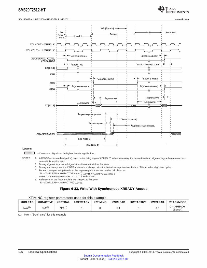
Lead 1Active
Trail
XCLKOUT = XTIMCLK
XCLKOUT = 1/2 XTIMCLK
XA[0:18]
XD[0:15]
XREADY(Synch)
td(XCOHL-XWEL) td(XCOHL-XWEH)
td(XCOHL-XZCSH)
td(XCOH-XA)
WS (Synch)
XZCS0AND1, XZCS2,XZCS6AND7
XRD
XWE
XR/W
td(XCOH-XZCSL)
NOTES: A. All XINTF accesses (lead period) begin on the rising edge of XCLKOUT. When necessary, the device inserts an alignment cycle before an accessto meet this requirement.
B. During alignment cycles, all signals transitions to their inactive state.C. During inactive cycles, the XINTF address bus always holds the last address put out on the bus. This includes alignment cycles.D. For each sample, setup time from the beginning of the access can be calculated as
D = (XWRLEAD + XWRACTIVE + n − 1) tc(XTIM) − tsu(XRDYsynchL)XCOHLwhere n is the sample number: n = 1, 2, 3 and so forth.
E. Reference for the first sample is with respect to this point E = (XWRLEAD + XWRACTIVE) tc(XTIM)
td(XCOH-XRNWL) td(XCOHL-XRNWH)
ten(XD)XWELth(XD)XWEH
tsu(XRDHsynchH)XCOHL
tsu(XRDYsynchL)XCOHL
DOUT
td(XWEL-XD
)
tdis(XD)XRNW
th(XRDYsynchL)
th(XRDYsynchH)XZCSH
= Don’t care. Signal can be high or low during this time.
Legend:
See Note E
See Note D
SeeNotes Aand B
See Note C
te(XRDYsynchH)
SM320F2812-HT
SGUS062B–JUNE 2009–REVISED JUNE 2011 www.ti.com
Figure 6-33. Write With Synchronous XREADY Access
XTIMING register parameters used for this example:XRDLEAD XRDACTIVE XRDTRAIL USEREADY X2TIMING XWRLEAD XWRACTIVE XWRTRAIL READYMODE
0 = XREADYN/A (1) N/A (1) N/A (1) 1 0 ≥ 1 3 ≥ 1 (Synch)
(1) N/A = "Don't care" for this example
126 Electrical Specifications Copyright © 2009–2011, Texas Instruments Incorporated
Submit Documentation FeedbackProduct Folder Link(s): SM320F2812-HT

Lead 1Active
Trail
XCLKOUT = XTIMCLK
XCLKOUT = 1/2 XTIMCLK
XA[0:18]
XD[0:15]
td(XCOHL-XWEH)
td(XCOHL-XZCSH)
td(XCOH-XA)
WS (Asynch)
XZCS0AND1, XZCS2,XZCS6AND7
XRD
XWE
XR/W
td(XCOH-XZCSL)
NOTES: A. All XINTF accesses (lead period) begin on the rising edge of XCLKOUT. When necessary, the device inserts analignment cycle before an access to meet this requirement.
B. During alignment cycles, all signals transitions to their inactive state.C. During inactive cycles, the XINTF address bus always holds the last address put out on the bus. This includes alignment
cycles.D. For each sample, setup time from the beginning of the access can be calculated as:
D = (XWRLEAD + XWRACTIVE −3 + n) tc(XTIM) − tsu(XRDYasynchL)XCOHLwhere n is the sample number: n = 1, 2, 3 and so forth.
E. Reference for the first sample is with respect to this point E = (XWRLEAD + XWRACTIVE −2) tc(XTIM)
td(XCOH-XRNWL) td(XCOHL-XRNWH)
ten(XD)XWEL th(XD)XWEH
th(XRDYasynchL)
DOUT
tdis(XD)XRNW
th(XRDYasynchH)XZCSH
See Note E
See Note D
= Don’t care. Signal can be high or low during this time.
Legend:
tsu(XRDYasynchL)XCOHL
tsu(XRDYasynchH)XCOHL
td(XWEL-XD
)
td(XCOHL-XWEL)
te(XRDYasynchH)
XREADY(Asynch)
SM320F2812-HT
www.ti.com SGUS062B–JUNE 2009–REVISED JUNE 2011
Figure 6-34. Write With Asynchronous XREADY Access
XTIMING register parameters used for this example:XRDLEAD XRDACTIVE XRDTRAIL USEREADY X2TIMING XWRLEAD XWRACTIVE XWRTRAIL READYMODE
1 = XREADYN/A (1) N/A (1) N/A (1) 1 0 ≥ 1 3 ≥ 1 (Asynch)
(1) N/A = "Don't care" for this example
Copyright © 2009–2011, Texas Instruments Incorporated Electrical Specifications 127Submit Documentation Feedback
Product Folder Link(s): SM320F2812-HT
SM320F2812-HT
SGUS062B–JUNE 2009–REVISED JUNE 2011 www.ti.com
6.27 XHOLD and XHOLDA
f the HOLD mode bit is set while XHOLD and XHOLDA are both low (external bus accesses granted), theXHOLDA signal is forced high (at the end of the current cycle) and the external interface is taken out ofhigh-impedance mode.
On a reset (XRS), the HOLD mode bit is set to 0. If the XHOLD signal is active low on a system reset, thebus and all signal strobes must be in high-impedance mode, and the XHOLDA signal is also driven activelow.
When HOLD mode is enabled and XHOLDA is active low (external bus grant active), the CPU can stillexecute code from internal memory. If an access is made to the external interface, the CPU is stalled untilthe XHOLD signal is removed.
An external DMA request, when granted, places the following signals in a high-impedance mode:
XA[18:0] XZCS0AND1
XD[15:0] XZCS2
XWE, XRD XZCS6AND7
XR/W
All other signals not listed in this group remain in their default or functional operational modes during thesesignal events. Detailed timing diagram is released in a future revision of this data sheet.
128 Electrical Specifications Copyright © 2009–2011, Texas Instruments Incorporated
Submit Documentation FeedbackProduct Folder Link(s): SM320F2812-HT

XCLKOUT(/1 Mode)
XHOLD
XR/W,XZCS0AND1,
XZCS2,XZCS6AND7
XD[15:0] Valid
XHOLDA
td(HL-Hiz)
td(HH-HAH)
High-Impedance
XA[18:0] Valid ValidHigh-Impedance
td(HH-BV)td(HL-HAL)
See Note A See Note B
SM320F2812-HT
www.ti.com SGUS062B–JUNE 2009–REVISED JUNE 2011
6.28 XHOLD/XHOLDA Timing
Table 6-44. XHOLD/XHOLDA Timing Requirements (XCLKOUT = XTIMCLK) (1) (2) (3)
MIN MAX UNIT
td(HL–HiZ) Delay time, XHOLD low to Hi–Z on all Address, Data, and Control 4tc(XTIM) ns
td(HL–HAL) Delay time, XHOLD low to XHOLDA low 5tc(XTIM) ns
td(HH–HAH) Delay time, XHOLD high to XHOLDA high 3tc(XTIM) ns
td(HH–BV) Delay time, XHOLD high to Bus valid 4tc(XTIM) ns
(1) When a low signal is detected on XHOLD, all pending XINTF accesses are completed before the bus is placed in a high-impedancestate.
(2) The state of XHOLD is latched on the rising edge of XTIMCLK.(3) Not production tested.
A. All pending XINTF accesses are completed.B. Normal XINTF operation resumes.
Figure 6-35. External Interface Hold Waveform
Copyright © 2009–2011, Texas Instruments Incorporated Electrical Specifications 129Submit Documentation Feedback
Product Folder Link(s): SM320F2812-HT

See Note A See Note B
SM320F2812-HT
SGUS062B–JUNE 2009–REVISED JUNE 2011 www.ti.com
Table 6-45. XHOLD/XHOLDA Timing Requirements (XCLKOUT = 1/2 XTIMCLK) (1) (2) (3) (4)
MIN MAX UNIT
td(HL-HiZ) Delay time, XHOLD low to Hi-Z on all Address, Data, and Control 4tc(XTIM) + tc(XCO) ns
td(HL-HAL) Delay time, XHOLD low to XHOLDA low 4tc(XTIM) + 2tc(XCO) ns
td(HH-HAH) Delay time, XHOLD high to XHOLDA high 4tc(XTIM) ns
td(HH-BV) Delay time, XHOLD high to Bus valid 6tc(XTIM) ns
(1) When a low signal is detected on XHOLD, all pending XINTF accesses are completed before the bus is placed in a high-impedancestate.
(2) The state of XHOLD is latched on the rising edge of XTIMCLK.(3) After the XHOLD is detected low or high, all bus transitions and XHOLDA transitions occur with respect to the rising edge of XCLKOUT.
Thus, for this mode where XCLKOUT = 1/2 XTIMCLK, the transitions can occur up to 1 XTIMCLK cycle earlier than the maximum valuespecified.
(4) Not production tested.
A. All pending XINTF accesses are completed.B. Normal XINTF operation resumes.
Figure 6-36. XHOLD/XHOLDA Timing Requirements (XCLKOUT = 1/2 XTIMCLK)
130 Electrical Specifications Copyright © 2009–2011, Texas Instruments Incorporated
Submit Documentation FeedbackProduct Folder Link(s): SM320F2812-HT
SM320F2812-HT
www.ti.com SGUS062B–JUNE 2009–REVISED JUNE 2011
6.29 On-Chip Analog-to-Digital Converter
6.29.1 ADC Absolute Maximum RatingsVALUE (1) UNIT
VSSA1/VSSA2 to VDDA1/VDDA2/AVDDREFBG –0.3 to 4.6 VSupply voltage range
VSS1 to VDD1 –0.3 to 2.5 V
Analog Input (ADCIN) Clamp Current, total (max) (2) ±20 mA
(1) Unless otherwise noted, the absolute maximum ratings are specified over operating conditions. Stresses beyond those listed underAbsolute Maximum Ratings may cause permanent damage to the device. These are stress ratings only. Exposure toabsolute-maximum-rated conditions for extended periods may affect device reliability.
(2) The analog inputs have an internal clamping circuit that clamps the voltage to a diode drop above VDDA or below VSS. The continuousclamp current per pin is ±2 mA.
Copyright © 2009–2011, Texas Instruments Incorporated Electrical Specifications 131Submit Documentation Feedback
Product Folder Link(s): SM320F2812-HT
SM320F2812-HT
SGUS062B–JUNE 2009–REVISED JUNE 2011 www.ti.com
6.29.2 ADC Electrical Characteristics Over Recommended Operating Conditions
Table 6-46. DC Specifications (1) (2)
TA = –55°C to 220°CPARAMETER UNIT
MIN TYP MAX
Resolution 12 Bits
ADC clock (3) 1 kHz
25 MHz
ACCURACY
INL (Integral nonlinearity) (4) 1–18.75 MHz ADC clock ±1.5 LSB
DNL (Differential nonlinearity) (4) 1–18.75 MHz ADC clock ±1 LSB
Offset error (5) –80 80 LSB
Overall gain error with internal –200 200 LSBreference (6)
Overall gain error with external If ADCREFP-ADCREFM = 1 V ±0.1% –50 50 LSBreference (7)
Channel-to-channel offset variation ±8 LSB
Channel-to-channel Gain variation ±8 LSB
ANALOG INPUT
Analog input voltage (ADCINx to 0 3 VADCLO) (8)
ADCLO –5 0 5 mV
Input capacitance 10 pF
Input leakage current 3 ±5 μA
INTERNAL VOLTAGE REFERENCE (6)
Accuracy, ADCVREFP 1.9 2 2.1 V
Accuracy, ADCVREFM 0.95 1 1.05 V
Voltage difference, ADCREFP – 1 VADCREFM
Temperature coefficient 50 PPM/°CReference noise 100 V
EXTERNAL VOLTAGE REFERENCE (7)
Accuracy, ADCVREFP 1.9 2 2.1 V
Accuracy, ADCVREFM 0.95 1 1.05 V
Input voltage difference, ADCREFP – 0.99 1 1.01 VADCREFM
(1) Not production tested.(2) Tested at 12.5-MHz ADCCLK(3) If SYSCLKOUT ≤ 25 MHz, ADC clock ≤ SYSCLKOUT/2(4) The INL degrades for frequencies beyond 18.75 MHz –25 MHz. Applications that require these sampling rates should use a 20-kΩ
resistor as bias resistor on the ADCRESEXT pin. This improves overall linearity and typical current drawn by the ADC is a few mA morethan 24.9 kW bias.
(5) 1 LSB has the weighted value of 3.0/4096 = 0.732 mV.(6) A single internal band gap reference (±5% accuracy) sources both ADCREFP and ADCREFM signals, and hence, these voltages track
together. The ADC converter uses the difference between these two as its reference. The total gain error is the combination of the gainerror shown here and the voltage reference accuracy (ADCREFP – ADCREFM). A software-based calibration procedure isrecommended for better accuracy. See F2812 ADC Calibration Application Note (SPRA989) and Section 5.2, Documentation Support,for relevant documents.
(7) In this mode, the accuracy of external reference is critical for overall gain. The voltage difference (ADCREFP–ADCREFM) determinesthe overall accuracy.
(8) Voltages above VDDA + 0.3 V or below VSS – 0.3 V applied to an analog input pin may temporarily affect the conversion of another pin.To avoid this, the analog inputs should be kept within these limits.
132 Electrical Specifications Copyright © 2009–2011, Texas Instruments Incorporated
Submit Documentation FeedbackProduct Folder Link(s): SM320F2812-HT

SM320F2812-HT
www.ti.com SGUS062B–JUNE 2009–REVISED JUNE 2011
Table 6-47. AC Specifications (1) (2)
TA = –55°C to 125°C TA = 220°CPARAMETER UNIT
MIN TYP MAX MIN TYP MAX
SINAD Signal-to-noise ratio + distortion 62 57 dB
SNR Signal-to-noise ratio 62 57 dB
THD Total harmonic distortion -68 -68 dB
ENOB (SNR) Effective number of bits 10.1 9.1 Bits
SFDR Spurious free dynamic range 69 68 dB
(1) Not production tested.(2) Validated at the following conditions: ADC Input Frequency = 10.71 KHz, XCLKIN = 30 MHz, PLLCR = 0xA (SYSCLK = 150 MHz),
HSPCP = 3 (ADCCLK= 25 MHz), ADCCLKPS = 1 (ADCCLK= 12.5 MHz), CPS = 0 (ADCCLK =12.5 MHZ), ACQ_PS (SH) = 3
6.29.3 Current Consumption for Different ADC Configurations (at 25-MHz ADCCLK)
Table 6-48. Current Consumption (1)
IDDA (TYP) (2) IDDAIO (TYP) IDD1 (TYP) ADC OPERATING MODE/CONDITIONS (3)
Mode A (Operational Mode):
40 mA 1 μA 0.5 mA –BG and REF enabled
–PWD disabled
Mode B:
–ADC clock enabled7 mA 0 5 μA
–BG and REF enabled
–PWD enabled
Mode C:
–ADC clock enabled1 μA 0 5 μA
–BG and REF disabled
–PWD enabled
Mode D:
–ADC clock disabled1 μA 0 0
–BG and REF disabled
–PWD enabled
(1) Not production tested.(2) IDDA – includes current into VDDA1/ VDDA2 and AVDDREFBG(3) Test Conditions: SYSCLKOUT = 150 MHz
ADC module clock = 25 MHzADC performing a continuous conversion of all 16 channels in Mode A
Copyright © 2009–2011, Texas Instruments Incorporated Electrical Specifications 133Submit Documentation Feedback
Product Folder Link(s): SM320F2812-HT

ac
Rs ADCIN0
Cp10 pF
Ron1 kΩ
1.25 pFCh
Switch
Typical Values of the Input Circuit Components:
Switch Resistance (Ron): 1 kΩSampling Capacitor (Ch): 1.25 pFParasitic Capacitance (Cp): 10 pFSource Resistance (Rs): 50 Ω
28x DSP
SourceSignal
ADC Power Up Delay ADC Ready for Conversions
PWDNBG
PWDNREF
PWDNADC
Request forADC
Conversion
td(BGR)
td(PWD)
SM320F2812-HT
SGUS062B–JUNE 2009–REVISED JUNE 2011 www.ti.com
Figure 6-37. ADC Analog Input Impedance Model
6.29.4 ADC Power-Up Control Bit Timing
Figure 6-38. ADC Power-Up Control Bit Timing
Table 6-49. ADC Power-Up Delays (1) (2)
MIN TYP MAX UNIT
Delay time for band gap reference to be stable. Bits 6 and 5 of the ADCTRL3 registertd(BGR) 7 8 10 ms(PWDNBG and PWDNREF) are to be set to 1 before the ADCPWDN bit is enabled.
20 50 μsDelay time for power-down control to be stable. Bit 7 of the ADCTRL3 register (ADCPWDN)td(PWD) is to be set to 1 before any ADC conversions are initiated. 1 ms
(1) These delays are necessary and recommended to make the ADC analog reference circuit stable before conversions are initiated. Ifconversions are started without these delays, the ADC results shows a higher gain. For power down, all three bits can be cleared at thesame time.
(2) Not production tested.
134 Electrical Specifications Copyright © 2009–2011, Texas Instruments Incorporated
Submit Documentation FeedbackProduct Folder Link(s): SM320F2812-HT

Analog Input onChannel Ax or Bx
ADC Clock
Sample and HoldSH Pulse
SMODE Bit
tdschx_n
tdschx_n+1
Sample n
Sample n+1Sample n+2
tSH
ADC Event Trigger fromEV or Other Sources
td(SH)
SM320F2812-HT
www.ti.com SGUS062B–JUNE 2009–REVISED JUNE 2011
6.29.5 Detailed Description
6.29.5.1 Reference Voltage
The on-chip ADC has a built-in reference, which provides the reference voltages for the ADC. ADCVREFPis set to 2 V and ADCVREFM is set to 1 V.
6.29.5.2 Analog Inputs
The on-chip ADC consists of 16 analog inputs, which are sampled either one at a time or two channels ata time. These inputs are software-selectable.
6.29.5.3 Converter
The on-chip ADC uses a 12-bit four-stage pipeline architecture, which achieves a high sample rate withlow power consumption.
6.29.5.4 Conversion Modes
The conversion can be performed in two different conversion modes:• Sequential sampling mode (SMODE = 0)• Simultaneous sampling mode (SMODE = 1)
6.29.6 Sequential Sampling Mode (Single Channel) (SMODE = 0)
In sequential sampling mode, the ADC can continuously convert input signals on any of the channels (Axto Bx). The ADC can start conversions on event triggers from the Event Managers (EVA/EVB), softwaretrigger, or from an external ADCSOC signal. If the SMODE bit is 0, the ADC does conversions on theselected channel on every Sample/Hold pulse. The conversion time and latency of the Result registerupdate are explained below. The ADC interrupt flags are set a few SYSCLKOUT cycles after the Resultregister update. The selected channel is sampled at every falling edge of the Sample/Hold pulse. TheSample/Hold pulse width can be programmed to be one ADC clock wide (minimum) or 16 ADC clockswide (maximum).
Figure 6-39. Sequential Sampling Mode (Single-Channel) Timing
Copyright © 2009–2011, Texas Instruments Incorporated Electrical Specifications 135Submit Documentation Feedback
Product Folder Link(s): SM320F2812-HT
SM320F2812-HT
SGUS062B–JUNE 2009–REVISED JUNE 2011 www.ti.com
Table 6-50. Sequential Sampling Mode Timing (1)
AT 25–MHz ADCSAMPLE n SAMPLE n + 1 CLOCK, REMARKS
tc(ADCCLK) = 40 ns
Delay time from event trigger totd(SH) 2.5tc(ADCCLK)sampling
(1 + Acqps) × Acqps value = 0-15tSH Sample/Hold width/Acquisition width 40 ns with Acqps = 0tc(ADCCLK) ADCTRL1[8:11]
Delay time for first result to appeartd(schx_n) 4tc(ADCCLK) 160 nsin the Result register
Delay time for successive results to (2 + Acqps) ×td(schx_n+1) 80 nsappear in the Result register tc(ADCCLK)
(1) Not production tested.
136 Electrical Specifications Copyright © 2009–2011, Texas Instruments Incorporated
Submit Documentation FeedbackProduct Folder Link(s): SM320F2812-HT
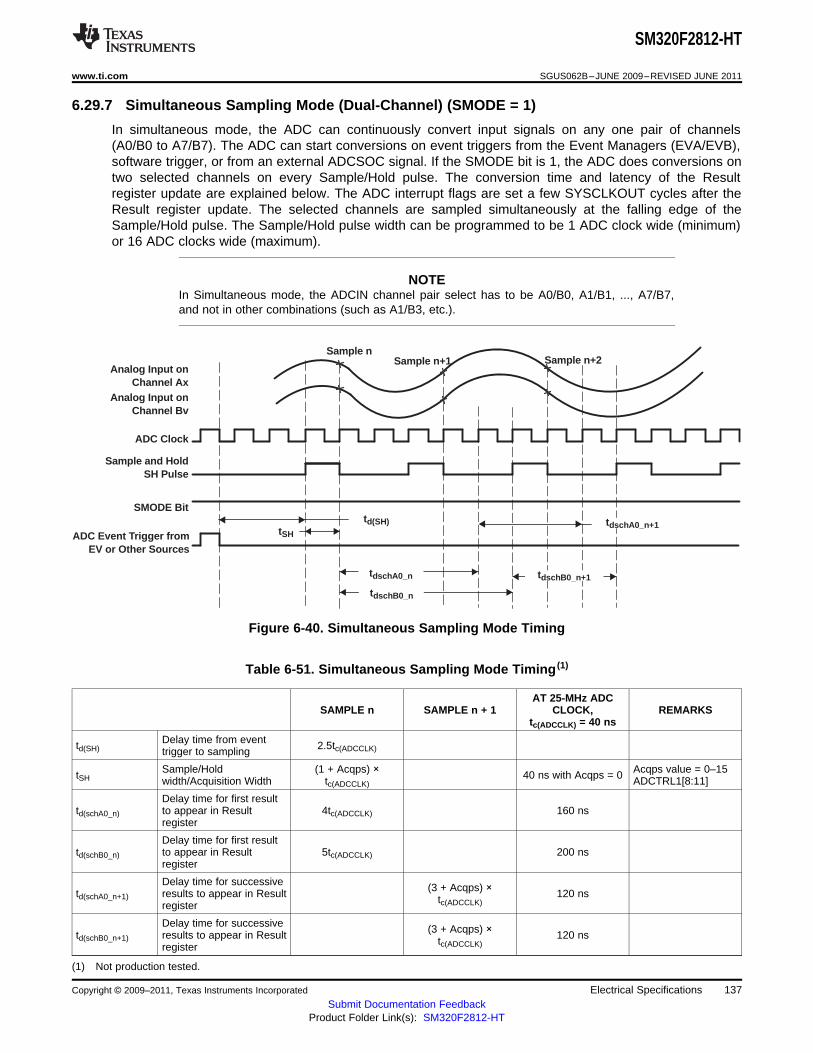
Analog Input onChannel Ax
Analog Input onChannel Bv
ADC Clock
Sample and HoldSH Pulse
tSH
tdschA0_n
tdschB0_n
tdschB0_n+1
Sample nSample n+1 Sample n+2
tdschA0_n+1td(SH)
ADC Event Trigger fromEV or Other Sources
SMODE Bit
SM320F2812-HT
www.ti.com SGUS062B–JUNE 2009–REVISED JUNE 2011
6.29.7 Simultaneous Sampling Mode (Dual-Channel) (SMODE = 1)
In simultaneous mode, the ADC can continuously convert input signals on any one pair of channels(A0/B0 to A7/B7). The ADC can start conversions on event triggers from the Event Managers (EVA/EVB),software trigger, or from an external ADCSOC signal. If the SMODE bit is 1, the ADC does conversions ontwo selected channels on every Sample/Hold pulse. The conversion time and latency of the Resultregister update are explained below. The ADC interrupt flags are set a few SYSCLKOUT cycles after theResult register update. The selected channels are sampled simultaneously at the falling edge of theSample/Hold pulse. The Sample/Hold pulse width can be programmed to be 1 ADC clock wide (minimum)or 16 ADC clocks wide (maximum).
NOTEIn Simultaneous mode, the ADCIN channel pair select has to be A0/B0, A1/B1, ..., A7/B7,and not in other combinations (such as A1/B3, etc.).
Figure 6-40. Simultaneous Sampling Mode Timing
Table 6-51. Simultaneous Sampling Mode Timing (1)
AT 25-MHz ADCSAMPLE n SAMPLE n + 1 CLOCK, REMARKS
tc(ADCCLK) = 40 ns
Delay time from eventtd(SH) 2.5tc(ADCCLK)trigger to sampling
Sample/Hold (1 + Acqps) × Acqps value = 0–15tSH 40 ns with Acqps = 0width/Acquisition Width tc(ADCCLK) ADCTRL1[8:11]
Delay time for first resulttd(schA0_n) to appear in Result 4tc(ADCCLK) 160 ns
register
Delay time for first resulttd(schB0_n) to appear in Result 5tc(ADCCLK) 200 ns
register
Delay time for successive (3 + Acqps) ×td(schA0_n+1) results to appear in Result 120 nstc(ADCCLK)register
Delay time for successive (3 + Acqps) ×td(schB0_n+1) results to appear in Result 120 nstc(ADCCLK)register
(1) Not production tested.
Copyright © 2009–2011, Texas Instruments Incorporated Electrical Specifications 137Submit Documentation Feedback
Product Folder Link(s): SM320F2812-HT

(SINAD 1.76)N
6.02
-
=
SM320F2812-HT
SGUS062B–JUNE 2009–REVISED JUNE 2011 www.ti.com
6.29.8 Definitions of Specifications and Terminology
6.29.8.1 Integral Nonlinearity
Integral nonlinearity refers to the deviation of each individual code from a line drawn from zero through fullscale. The point used as zero occurs 1/2 LSB before the first code transition. The full-scale point isdefined as level 1/2 LSB beyond the last code transition. The deviation is measured from the center ofeach particular code to the true straight line between these two points.
6.29.8.2 Differential Nonlinearity
An ideal ADC exhibits code transitions that are exactly 1 LSB apart. DNL is the deviation from this idealvalue. A differential nonlinearity error of less than ±1 LSB ensures no missing codes.
6.29.8.3 Zero Offset
The major carry transition should occur when the analog input is at zero volts. Zero error is defined as thedeviation of the actual transition from that point.
6.29.8.4 Gain Error
The first code transition should occur at an analog value 1/2 LSB above negative full scale. The lasttransition should occur at an analog value 1 1/2 LSB below the nominal full scale. Gain error is thedeviation of the actual difference between first and last code transitions and the ideal difference betweenfirst and last code transitions.
6.29.8.5 Signal-to-Noise Ratio + Distortion (SINAD)
SINAD is the ratio of the rms value of the measured input signal to the rms sum of all other spectralcomponents below the Nyquist frequency, including harmonics but excluding dc. The value for SINAD isexpressed in decibels.
6.29.8.6 Effective Number of Bits (ENOB)
For a sine wave, SINAD can be expressed in terms of the number of bits. Using the following formula,
it is possible to get a measure of performance expressed as N, the effective number of bits. Thus,effective number of bits for a device for sine wave inputs at a given input frequency can be calculateddirectly from its measured SINAD.
6.29.8.7 Total Harmonic Distortion (THD)
THD is the ratio of the rms sum of the first six harmonic components to the rms value of the measuredinput signal and is expressed as a percentage or in decibels.
6.29.8.8 Spurious Free Dynamic Range (SFDR)
SFDR is the difference in dB between the rms amplitude of the input signal and the peak spurious signal.
138 Electrical Specifications Copyright © 2009–2011, Texas Instruments Incorporated
Submit Documentation FeedbackProduct Folder Link(s): SM320F2812-HT

CLKG CLKSRG
(1 CLKGDV)(2) 2P = 1/CLKG in ns. CLKG is the output of sample rate generator mux.
SM320F2812-HT
www.ti.com SGUS062B–JUNE 2009–REVISED JUNE 2011
6.30 Multichannel Buffered Serial Port (McBSP) Timing
6.30.1 McBSP Transmit and Receive Timing
Table 6-52. McBSP Timing Requirements (1) (2) (3)
NO. MIN MAX UNIT
1 kHzMcBSP module clock (CLKG, CLKX, CLKR) range
20 (4) MHz
50 nsMcBSP module cycle time (CLKG, CLKX, CLKR) range
1 ms
M11 tc(CKRX) Cycle time, CLKR/X CLKR/X ext 2P ns
M12 tw(CKRX) Pulse duration, CLKR/X high or CLKR/X low CLKR/X ext P–7 ns
M13 tr(CKRX) Rise time, CLKR/X CLKR/X ext 7 ns
M14 tf(CKRX) Fall time, CLKR/X CLKR/X ext 7 ns
CLKR int 18M15 tsu(FRH-CKRL) Setup time, external FSR high before CLKR low ns
CLKR ext 2
CLKR int 0M16 th(CKRL-FRH) Hold time, external FSR high after CLKR low ns
CLKR ext 6
CLKR int 18M17 tsu(DRV-CKRL) Setup time, DR valid before CLKR low ns
CLKR ext 2
CLKR int 0M18 th(CKRL-DRV) Hold time, DR valid after CLKR low ns
CLKR ext 6
CLKX int 18M19 tsu(FXH-CKXL) Setup time, external FSX high before CLKX low ns
CLKX ext 2
CLKX int 0M20 th(CKXL-FXH) Hold time, external FSX high after CLKX low ns
CLKX ext 6
(1) Polarity bits CLKRP = CLKXP = FSRP = FSXP = 0. If the polarity of any of the signals is inverted, then the timing references of thatsignal are also inverted.Polarity bits CLKRP = CLKXP = FSRP = FSXP = 0. If the polarity of any of the signals is inverted, then thetiming references of that signal are also inverted.
CLKSRG can be LSPCLK, CLKX, CLKR as source. CLKSRG ≤ (SYSCLKOUT/2). McBSP performance is limited by I/O buffer switchingspeed.
(3) Not production tested.(4) Internal clock prescalers must be adjusted such that the McBSP clock (CLKG, CLKX, CLKR) speeds are not greater than the I/O buffer
speed limit (20 MHz).
Copyright © 2009–2011, Texas Instruments Incorporated Electrical Specifications 139Submit Documentation Feedback
Product Folder Link(s): SM320F2812-HT
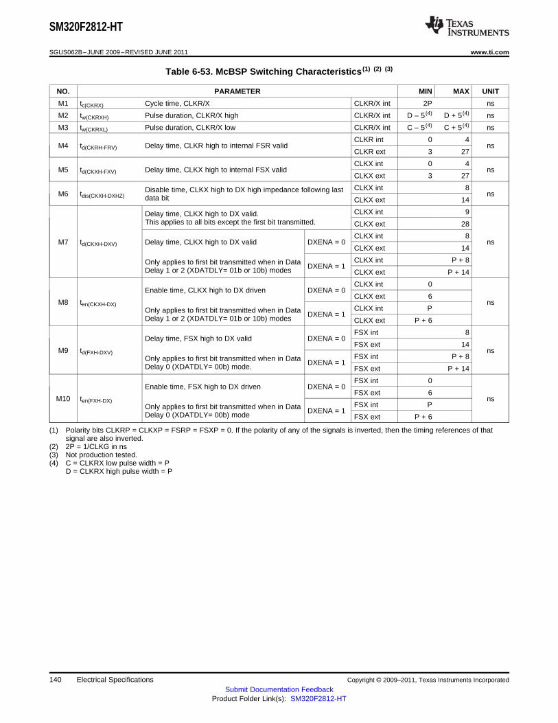
SM320F2812-HT
SGUS062B–JUNE 2009–REVISED JUNE 2011 www.ti.com
Table 6-53. McBSP Switching Characteristics (1) (2) (3)
NO. PARAMETER MIN MAX UNIT
M1 tc(CKRX) Cycle time, CLKR/X CLKR/X int 2P ns
M2 tw(CKRXH) Pulse duration, CLKR/X high CLKR/X int D – 5 (4) D + 5 (4) ns
M3 tw(CKRXL) Pulse duration, CLKR/X low CLKR/X int C – 5 (4) C + 5 (4) ns
CLKR int 0 4M4 td(CKRH-FRV) Delay time, CLKR high to internal FSR valid ns
CLKR ext 3 27
CLKX int 0 4M5 td(CKXH-FXV) Delay time, CLKX high to internal FSX valid ns
CLKX ext 3 27
CLKX int 8Disable time, CLKX high to DX high impedance following lastM6 tdis(CKXH-DXHZ) nsdata bit CLKX ext 14
CLKX int 9Delay time, CLKX high to DX valid.This applies to all bits except the first bit transmitted. CLKX ext 28
CLKX int 8M7 td(CKXH-DXV) Delay time, CLKX high to DX valid DXENA = 0 ns
CLKX ext 14
CLKX int P + 8Only applies to first bit transmitted when in Data DXENA = 1Delay 1 or 2 (XDATDLY= 01b or 10b) modes CLKX ext P + 14
CLKX int 0Enable time, CLKX high to DX driven DXENA = 0
CLKX ext 6M8 ten(CKXH-DX) ns
CLKX int POnly applies to first bit transmitted when in Data DXENA = 1Delay 1 or 2 (XDATDLY= 01b or 10b) modes CLKX ext P + 6
FSX int 8Delay time, FSX high to DX valid DXENA = 0
FSX ext 14M9 td(FXH-DXV) ns
FSX int P + 8Only applies to first bit transmitted when in Data DXENA = 1Delay 0 (XDATDLY= 00b) mode. FSX ext P + 14
FSX int 0Enable time, FSX high to DX driven DXENA = 0
FSX ext 6M10 ten(FXH-DX) ns
FSX int POnly applies to first bit transmitted when in Data DXENA = 1Delay 0 (XDATDLY= 00b) mode FSX ext P + 6
(1) Polarity bits CLKRP = CLKXP = FSRP = FSXP = 0. If the polarity of any of the signals is inverted, then the timing references of thatsignal are also inverted.
(2) 2P = 1/CLKG in ns(3) Not production tested.(4) C = CLKRX low pulse width = P
D = CLKRX high pulse width = P
140 Electrical Specifications Copyright © 2009–2011, Texas Instruments Incorporated
Submit Documentation FeedbackProduct Folder Link(s): SM320F2812-HT

(n−2)Bit (n−1)
(n−3)(n−2)Bit (n−1)
(n−4)(n−3)(n−2)Bit (n−1)
M18M17
M18M17
M17M18
M16M15
M4M4M14
M13M3, M12
M1, M11
M2, M12
(RDATDLY= 10b)DR
(RDATDLY= 01b)DR
(RDATDLY= 00b)DR
FSR (ext)
FSR (int)
CLKR
M8
M7
M7M8
M6
M7M9
M10
(XDATDLY= 10b)DX
(XDATDLY= 01b)DX
(XDATDLY= 00b)DX
(n−2)Bit (n−1)Bit 0
(n−4)Bit (n−1) (n−3)(n−2)Bit 0
(n−3)(n−2)Bit (n−1)Bit 0
M20
M14M13M3, M12
M1, M11M2, M12
FSX (ext)
FSX (int)
CLKX
M5M5
M19
SM320F2812-HT
www.ti.com SGUS062B–JUNE 2009–REVISED JUNE 2011
Figure 6-41. McBSP Receive Timing
Figure 6-42. McBSP Transmit Timing
Copyright © 2009–2011, Texas Instruments Incorporated Electrical Specifications 141Submit Documentation Feedback
Product Folder Link(s): SM320F2812-HT

Bit 0 Bit(n-1) (n-2) (n-3) (n-4)
Bit 0 Bit(n-1) (n-2) (n-3) (n-4)
CLKX
FSX
DX
M30M31
DR
M28
M24
M29
M25
LSB MSBM32 M33
SM320F2812-HT
SGUS062B–JUNE 2009–REVISED JUNE 2011 www.ti.com
6.30.2 McBSP as SPI Master or Slave Timing
Table 6-54. McBSP as SPI Master or Slave Timing Requirements (CLKSTP = 10b, CLKXP = 0) (1)
MASTER SLAVENO. UNIT
MIN MAX MIN MAX
M30 tsu(DRV0CKXL) Setup time, DR valid before CLKX low P – 10 8P – 10 ns
M31 th(CKXL0DRV) Hold time, DR valid after CLKX low P – 10 8P – 10 ns
M32 tsu(BFXL0CKXH) Setup time, FSX low before CLKX high 8P + 10 ns
M33 tc(CKX) Cycle time, CLKX 2P 16P ns
(1) Not production tested.
Table 6-55. McBSP as SPI Master or Slave Switching Characteristics (CLKSTP = 10b, CLKXP = 0) (1) (2)
MASTER SLAVENO. PARAMETER UNIT
MIN MAX MIN MAX
M24 th(CKXL0FXL) Hold time, FSX low after CLKX low 2P ns
M25 td(FXL0CKXH) Delay time, FSX low to CLKX high P ns
Disable time, DX high impedance following last data bit fromM28 tdis(FXH0DXHZ) 6 6P + 6 nsFSX high
M29 td(FXL0DXV) Delay time, FSX low to DX valid 6 4P + 6 ns
(1) Not production tested.(2) 2P = 1/CLKG
For all SPI slave modes, CLKX has to be minimum eight CLKG cycles. Also, CLKG should be LSPCLK/2 by setting CLKSM = CLKGDV= 1. With maximum LSPCLK speed of 75 MHz, CLKX maximum frequency is LSPCLK/16, that is 4.5 MHz and P = 13.3 ns.
Figure 6-43. McBSP Timing as SPI Master or Slave: CLKSTP = 10b, CLKXP = 0
142 Electrical Specifications Copyright © 2009–2011, Texas Instruments Incorporated
Submit Documentation FeedbackProduct Folder Link(s): SM320F2812-HT

Bit 0 Bit(n-1) (n-2) (n-3) (n-4)
Bit 0 Bit(n-1) (n-2) (n-3) (n-4)
CLKX
FSX
DX
DR
M35
M37
M40M39
M38
M34
LSB MSBM41 M42
SM320F2812-HT
www.ti.com SGUS062B–JUNE 2009–REVISED JUNE 2011
Table 6-56. McBSP as SPI Master or Slave Timing Requirements (CLKSTP = 11b, CLKXP = 0) (1)
MASTER SLAVENO. UNIT
MIN MAX MIN MAX
M39 tsu(DRV-CKXH) Setup time, DR valid before CLKX high P – 10 8P – 10 ns
M40 th(CKXH-DRV) Hold time, DR valid after CLKX high P – 10 8P – 10 ns
M41 tsu(FXL-CKXH) Setup time, FSX low before CLKX high 16P + 10 ns
M42 tc(CKX) Cycle time, CLKX 2P 16P ns
(1) Not production tested.
Table 6-57. McBSP as SPI Master or Slave Switching Characteristics (CLKSTP = 11b, CLKXP = 0) (1) (2)
MASTER SLAVENO. PARAMETER UNIT
MIN MAX MIN MAX
M34 th(CKXL-FXL) Hold time, FSX low after CLKX low P ns
M35 td(FXL-CKXH) Delay time, FSX low to CLKX high 2P ns
Disable time, DX high impedance following last data bitM37 tdis(CKXL-DXHZ) P + 6 7P + 6 nsfrom CLKX low
M38 td(FXL-DXV) Delay time, FSX low to DX valid 6 4P + 6 ns
(1) Not production tested.(2) 2P = 1/CLKG
For all SPI slave modes, CLKX has to be minimum eight CLKG cycles. Also, CLKG should be LSPCLK/2 by setting CLKSM = CLKGDV= 1. With maximum LSPCLK speed of 75 MHz, CLKX maximum frequency is LSPCLK/16 , that is 4.5 MHz and P = 13.3 ns.
Figure 6-44. McBSP Timing as SPI Master or Slave: CLKSTP = 11b, CLKXP = 0
Copyright © 2009–2011, Texas Instruments Incorporated Electrical Specifications 143Submit Documentation Feedback
Product Folder Link(s): SM320F2812-HT

M51
M50
M47
Bit 0 Bit(n-1) (n-2) (n-3) (n-4)
Bit 0 Bit(n-1) (n-2) (n-3) (n-4)
CLKX
FSX
DX
DR
M44
M48
M49
M43
LSB MSB M52
SM320F2812-HT
SGUS062B–JUNE 2009–REVISED JUNE 2011 www.ti.com
Table 6-58. McBSP as SPI Master or Slave Timing Requirements (CLKSTP = 10b, CLKXP = 1) (1)
MASTER SLAVENO. UNIT
MIN MAX MIN MAX
M49 tsu(DRV-CKXH) Setup time, DR valid before CLKX high P – 10 8P – 10 ns
M50 th(CKXH-DRV) Hold time, DR valid after CLKX high P – 10 8P – 10 ns
M51 tsu(FXL-CKXL) Setup time, FSX low before CLKX low 8P + 10 ns
M52 tc(CKX) Cycle time, CLKX 2P 16P ns
(1) Not production tested.
Table 6-59. McBSP as SPI Master or Slave Switching Characteristics (CLKSTP = 10b, CLKXP = 1) (1) (2)
MASTER SLAVENO. PARAMETER UNIT
MIN MAX MIN MAX
M43 th(CKXH-FXL) Hold time, FSX low after CLKX high 2P ns
M44 td(FXL-CKXL) Delay time, FSX low to CLKX low P ns
Disable time, DX high impedance following last data bit from FSXM47 tdis(FXH-DXHZ) 6 6P + 6 nshigh
M48 td(FXL-DXV) Delay time, FSX low to DX valid 6 4P + 6 ns
(1) Not production tested.(2) 2P = 1/CLKG
For all SPI slave modes, CLKX has to be minimum eight CLKG cycles. Also, CLKG should be LSPCLK/2 by setting CLKSM = CLKGDV= 1. With maximum LSPCLK speed of 75 MHz, CLKX maximum frequency is LSPCLK/16 , that is 4.5 MHz and P = 13.3 ns.
Figure 6-45. McBSP Timing as SPI Master or Slave: CLKSTP = 10b, CLKXP = 1
144 Electrical Specifications Copyright © 2009–2011, Texas Instruments Incorporated
Submit Documentation FeedbackProduct Folder Link(s): SM320F2812-HT
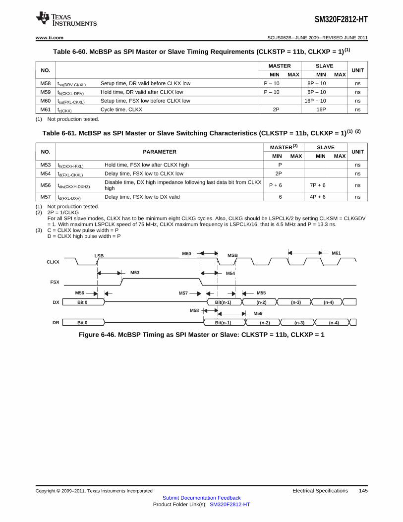
Bit 0 Bit(n-1) (n-2) (n-3) (n-4)
Bit 0 Bit(n-1) (n-2) (n-3) (n-4)
CLKX
FSX
DX
DR
M54
M58
M56
M53
M55
M59
M57
LSB MSBM60 M61
SM320F2812-HT
www.ti.com SGUS062B–JUNE 2009–REVISED JUNE 2011
Table 6-60. McBSP as SPI Master or Slave Timing Requirements (CLKSTP = 11b, CLKXP = 1) (1)
MASTER SLAVENO. UNIT
MIN MAX MIN MAX
M58 tsu(DRV-CKXL) Setup time, DR valid before CLKX low P – 10 8P – 10 ns
M59 th(CKXL-DRV) Hold time, DR valid after CLKX low P – 10 8P – 10 ns
M60 tsu(FXL-CKXL) Setup time, FSX low before CLKX low 16P + 10 ns
M61 tc(CKX) Cycle time, CLKX 2P 16P ns
(1) Not production tested.
Table 6-61. McBSP as SPI Master or Slave Switching Characteristics (CLKSTP = 11b, CLKXP = 1) (1) (2)
MASTER (3) SLAVENO. PARAMETER UNIT
MIN MAX MIN MAX
M53 th(CKXH-FXL) Hold time, FSX low after CLKX high P ns
M54 td(FXL-CKXL) Delay time, FSX low to CLKX low 2P ns
Disable time, DX high impedance following last data bit from CLKXM56 tdis(CKXH-DXHZ) P + 6 7P + 6 nshigh
M57 td(FXL-DXV) Delay time, FSX low to DX valid 6 4P + 6 ns
(1) Not production tested.(2) 2P = 1/CLKG
For all SPI slave modes, CLKX has to be minimum eight CLKG cycles. Also, CLKG should be LSPCLK/2 by setting CLKSM = CLKGDV= 1. With maximum LSPCLK speed of 75 MHz, CLKX maximum frequency is LSPCLK/16, that is 4.5 MHz and P = 13.3 ns.
(3) C = CLKX low pulse width = PD = CLKX high pulse width = P
Figure 6-46. McBSP Timing as SPI Master or Slave: CLKSTP = 11b, CLKXP = 1
Copyright © 2009–2011, Texas Instruments Incorporated Electrical Specifications 145Submit Documentation Feedback
Product Folder Link(s): SM320F2812-HT

SM320F2812-HT
SGUS062B–JUNE 2009–REVISED JUNE 2011 www.ti.com
6.31 Flash Timing
6.31.1 Recommended Operating Conditions
Table 6-62. Flash Endurance Timing (1) (2)
ERASE/PROGRAM MIN NOM MAX UNITTEMPERATURE
Nf Flash endurance for the array (write/erase cycles) -40°C to 125°C (ambient) 20000 (3) 50000 (3) cycles
NOTP OTP endurance for the array (write cycles) -40°C to 125°C (ambient) 1 write
(1) Write/erase operations outside of the temperature ranges indicated are not specified and may affect the endurance numbers.(2) Flash Timing Endurance is the minimum number of write/erase or write cycles specified over a programming temperature range of -40°C
to 125°C. Flash reads are supported within the recommended operating conditions specified in section 6.2.(3) The write/erase cycle numbers of 20000 (MIN) and 50000 (TYP) are applicable only for silicon revision G. For older silicon revisions, the
write/erase cycle numbers of 100 (MIN) and 1000 (TYP) are applicable.
Table 6-63. Flash Parameters at 150-MHz SYSCLKOUT (1) (2)
PARAMETER MIN TYP MAX UNIT
16-Bit Word 35 μsProgram 8K Sector 170 msTime
16K Sector 320 ms
8K Sector 10 sErase Time
16K Sector 11 s
Erase 75 mAIDD3VFLP VDD3VFL current consumption during the Erase/Program cycle
Program 35 mA
IDDP VDD current consumption during Erase/Program cycle 140 mA
IDDIOP VDDIO current consumption during Erase/Program cycle 20 mA
(1) Typical parameters as seen at room temperature using flash API V1 including function call overhead.(2) Not production tested.
Table 6-64. Flash/OTP Access Timing (1) (2)
PARAMETER MIN TYP MAX UNIT
ta(fp) Paged Flash access time 36 ns
ta(fr) Random Flash access time 36 ns
ta(OTP) OTP access time 60 ns
(1) For 150 MHz, PAGE WS = 5 and RANDOM WS = 5For 135 MHz, PAGE WS = 4 and RANDOM WS = 4
(2) Not production tested.
146 Electrical Specifications Copyright © 2009–2011, Texas Instruments Incorporated
Submit Documentation FeedbackProduct Folder Link(s): SM320F2812-HT

SM320F2812-HT
www.ti.com SGUS062B–JUNE 2009–REVISED JUNE 2011
Table 6-65. Minimum Required Wait-States at Different Frequencies (1)
SYSCLKOUT (MHz) SYSCLKOUT (ns) PAGE WAIT-STATE (2) RANDOM WAIT STATE (2) (3)
150 6.67 5 5
120 8.33 4 4
100 10 3 3
75 13.33 2 2
50 20 1 1
30 33.33 1 1
25 40 0 1
15 66.67 0 1
4 250 0 1
(1) Not production tested.(2) Formulas to compute page wait state and random wait state:
(3) Random wait state must be greater than or equal to 1
Copyright © 2009–2011, Texas Instruments Incorporated Electrical Specifications 147Submit Documentation Feedback
Product Folder Link(s): SM320F2812-HT

SM320F2812-HT
SGUS062B–JUNE 2009–REVISED JUNE 2011 www.ti.com
7 Mechanical Data
The following mechanical package diagram(s) reflect the most current released mechanical data availablefor the designated device(s).
148 Mechanical Data Copyright © 2009–2011, Texas Instruments Incorporated
Submit Documentation FeedbackProduct Folder Link(s): SM320F2812-HT

SM320F2812-HT
www.ti.com SGUS062B–JUNE 2009–REVISED JUNE 2011
Revision HistoryNOTE: Page numbers for previous revisions may differ from page numbers in the current version.
Changes from A Revision (April 2010) to B Revision .................................................................................................... Page
• Changed Table 3.31.1 Recommended Operating Conditions to Table 6-62. Flash Endurance Timing ............... 146
Copyright © 2009–2011, Texas Instruments Incorporated Mechanical Data 149Submit Documentation Feedback
Product Folder Link(s): SM320F2812-HT
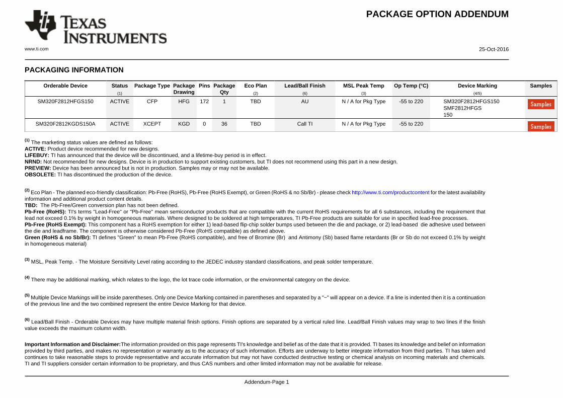
PACKAGE OPTION ADDENDUM
www.ti.com 25-Oct-2016
Addendum-Page 1
PACKAGING INFORMATION
Orderable Device Status(1)
Package Type PackageDrawing
Pins PackageQty
Eco Plan(2)
Lead/Ball Finish(6)
MSL Peak Temp(3)
Op Temp (°C) Device Marking(4/5)
Samples
SM320F2812HFGS150 ACTIVE CFP HFG 172 1 TBD AU N / A for Pkg Type -55 to 220 SM320F2812HFGS150SMF2812HFGS150
SM320F2812KGDS150A ACTIVE XCEPT KGD 0 36 TBD Call TI N / A for Pkg Type -55 to 220
(1) The marketing status values are defined as follows:ACTIVE: Product device recommended for new designs.LIFEBUY: TI has announced that the device will be discontinued, and a lifetime-buy period is in effect.NRND: Not recommended for new designs. Device is in production to support existing customers, but TI does not recommend using this part in a new design.PREVIEW: Device has been announced but is not in production. Samples may or may not be available.OBSOLETE: TI has discontinued the production of the device.
(2) Eco Plan - The planned eco-friendly classification: Pb-Free (RoHS), Pb-Free (RoHS Exempt), or Green (RoHS & no Sb/Br) - please check http://www.ti.com/productcontent for the latest availabilityinformation and additional product content details.TBD: The Pb-Free/Green conversion plan has not been defined.Pb-Free (RoHS): TI's terms "Lead-Free" or "Pb-Free" mean semiconductor products that are compatible with the current RoHS requirements for all 6 substances, including the requirement thatlead not exceed 0.1% by weight in homogeneous materials. Where designed to be soldered at high temperatures, TI Pb-Free products are suitable for use in specified lead-free processes.Pb-Free (RoHS Exempt): This component has a RoHS exemption for either 1) lead-based flip-chip solder bumps used between the die and package, or 2) lead-based die adhesive used betweenthe die and leadframe. The component is otherwise considered Pb-Free (RoHS compatible) as defined above.Green (RoHS & no Sb/Br): TI defines "Green" to mean Pb-Free (RoHS compatible), and free of Bromine (Br) and Antimony (Sb) based flame retardants (Br or Sb do not exceed 0.1% by weightin homogeneous material)
(3) MSL, Peak Temp. - The Moisture Sensitivity Level rating according to the JEDEC industry standard classifications, and peak solder temperature.
(4) There may be additional marking, which relates to the logo, the lot trace code information, or the environmental category on the device.
(5) Multiple Device Markings will be inside parentheses. Only one Device Marking contained in parentheses and separated by a "~" will appear on a device. If a line is indented then it is a continuationof the previous line and the two combined represent the entire Device Marking for that device.
(6) Lead/Ball Finish - Orderable Devices may have multiple material finish options. Finish options are separated by a vertical ruled line. Lead/Ball Finish values may wrap to two lines if the finishvalue exceeds the maximum column width.
Important Information and Disclaimer:The information provided on this page represents TI's knowledge and belief as of the date that it is provided. TI bases its knowledge and belief on informationprovided by third parties, and makes no representation or warranty as to the accuracy of such information. Efforts are underway to better integrate information from third parties. TI has taken andcontinues to take reasonable steps to provide representative and accurate information but may not have conducted destructive testing or chemical analysis on incoming materials and chemicals.TI and TI suppliers consider certain information to be proprietary, and thus CAS numbers and other limited information may not be available for release.
PACKAGE OPTION ADDENDUM
www.ti.com 25-Oct-2016
Addendum-Page 2
In no event shall TI's liability arising out of such information exceed the total purchase price of the TI part(s) at issue in this document sold by TI to Customer on an annual basis.
OTHER QUALIFIED VERSIONS OF SM320F2812-HT :
• Catalog: SM320F2812
• Enhanced Product: SM320F2812-EP
NOTE: Qualified Version Definitions:
• Catalog - TI's standard catalog product
• Enhanced Product - Supports Defense, Aerospace and Medical Applications


IMPORTANT NOTICE
Texas Instruments Incorporated and its subsidiaries (TI) reserve the right to make corrections, enhancements, improvements and otherchanges to its semiconductor products and services per JESD46, latest issue, and to discontinue any product or service per JESD48, latestissue. Buyers should obtain the latest relevant information before placing orders and should verify that such information is current andcomplete. All semiconductor products (also referred to herein as “components”) are sold subject to TI’s terms and conditions of salesupplied at the time of order acknowledgment.TI warrants performance of its components to the specifications applicable at the time of sale, in accordance with the warranty in TI’s termsand conditions of sale of semiconductor products. Testing and other quality control techniques are used to the extent TI deems necessaryto support this warranty. Except where mandated by applicable law, testing of all parameters of each component is not necessarilyperformed.TI assumes no liability for applications assistance or the design of Buyers’ products. Buyers are responsible for their products andapplications using TI components. To minimize the risks associated with Buyers’ products and applications, Buyers should provideadequate design and operating safeguards.TI does not warrant or represent that any license, either express or implied, is granted under any patent right, copyright, mask work right, orother intellectual property right relating to any combination, machine, or process in which TI components or services are used. Informationpublished by TI regarding third-party products or services does not constitute a license to use such products or services or a warranty orendorsement thereof. Use of such information may require a license from a third party under the patents or other intellectual property of thethird party, or a license from TI under the patents or other intellectual property of TI.Reproduction of significant portions of TI information in TI data books or data sheets is permissible only if reproduction is without alterationand is accompanied by all associated warranties, conditions, limitations, and notices. TI is not responsible or liable for such altereddocumentation. Information of third parties may be subject to additional restrictions.Resale of TI components or services with statements different from or beyond the parameters stated by TI for that component or servicevoids all express and any implied warranties for the associated TI component or service and is an unfair and deceptive business practice.TI is not responsible or liable for any such statements.Buyer acknowledges and agrees that it is solely responsible for compliance with all legal, regulatory and safety-related requirementsconcerning its products, and any use of TI components in its applications, notwithstanding any applications-related information or supportthat may be provided by TI. Buyer represents and agrees that it has all the necessary expertise to create and implement safeguards whichanticipate dangerous consequences of failures, monitor failures and their consequences, lessen the likelihood of failures that might causeharm and take appropriate remedial actions. Buyer will fully indemnify TI and its representatives against any damages arising out of the useof any TI components in safety-critical applications.In some cases, TI components may be promoted specifically to facilitate safety-related applications. With such components, TI’s goal is tohelp enable customers to design and create their own end-product solutions that meet applicable functional safety standards andrequirements. Nonetheless, such components are subject to these terms.No TI components are authorized for use in FDA Class III (or similar life-critical medical equipment) unless authorized officers of the partieshave executed a special agreement specifically governing such use.Only those TI components which TI has specifically designated as military grade or “enhanced plastic” are designed and intended for use inmilitary/aerospace applications or environments. Buyer acknowledges and agrees that any military or aerospace use of TI componentswhich have not been so designated is solely at the Buyer's risk, and that Buyer is solely responsible for compliance with all legal andregulatory requirements in connection with such use.TI has specifically designated certain components as meeting ISO/TS16949 requirements, mainly for automotive use. In any case of use ofnon-designated products, TI will not be responsible for any failure to meet ISO/TS16949.
Products ApplicationsAudio www.ti.com/audio Automotive and Transportation www.ti.com/automotiveAmplifiers amplifier.ti.com Communications and Telecom www.ti.com/communicationsData Converters dataconverter.ti.com Computers and Peripherals www.ti.com/computersDLP® Products www.dlp.com Consumer Electronics www.ti.com/consumer-appsDSP dsp.ti.com Energy and Lighting www.ti.com/energyClocks and Timers www.ti.com/clocks Industrial www.ti.com/industrialInterface interface.ti.com Medical www.ti.com/medicalLogic logic.ti.com Security www.ti.com/securityPower Mgmt power.ti.com Space, Avionics and Defense www.ti.com/space-avionics-defenseMicrocontrollers microcontroller.ti.com Video and Imaging www.ti.com/videoRFID www.ti-rfid.comOMAP Applications Processors www.ti.com/omap TI E2E Community e2e.ti.comWireless Connectivity www.ti.com/wirelessconnectivity
Mailing Address: Texas Instruments, Post Office Box 655303, Dallas, Texas 75265Copyright © 2016, Texas Instruments Incorporated