digital temperature sensor with a two-wire interface
TRANSCRIPT

FEATURES� TWO ADDRESSES
� DIGITAL OUTPUT: Two-Wire Serial Interface
� RESOLUTION: 9- to 12-Bits, User-Selectable
� ACCURACY:±2.0°C (max) from −25 °C to +85°C±3.0°C (max) from −40 °C to +125°C
� LOW QUIESCENT CURRENT:50µA, 0.1µA Standby
� NO POWER-UP SEQUENCE REQUIRED, I2CPULLUPS CAN BE ENABLED PRIOR TO V+
APPLICATIONS� NOTEBOOK COMPUTERS
� COMPUTER PERIPHERAL THERMALPROTECTION
� CELL PHONES
� BATTERY MANAGEMENT
� THERMOSTAT CONTROLS
� ENVIRONMENTAL MONITORING AND HVAC
0
A1
B1
C1
A2
B2
C2
SDA
SCL
V+
GND
ALERT
A0
YZC LEAD−FREE2 X 3 ARRAY(TOP VIEW)
Note: Pin A1 is marked with a for Pb−free (YZC)
1,65 mm1,50 mm
1,15 mm1,00 mm
(Bump Side Down)
‘ ’
DESCRIPTIONThe TMP106 is a two-wire, serial output temperaturesensor available in a WCSP package. Requiring noexternal components, the TMP106 is capable of readingtemperatures with a resolution of 0.0625°C.
The TMP106 features a Two-Wire interface that isSMBus-compatible, with the TMP106 allowing up to twodevices on one bus. The TMP106 also features an SMBusAlert function.
The TMP106 is ideal for extended temperaturemeasurement in a variety of communication, computer,consumer, environmental, industrial, and instrumentationapplications.
The TMP106 is specified for operation over a temperaturerange of −40°C to +125°C.
DiodeTemp.Sensor
∆ΣA/D
Converter
OSC
ControlLogic
SerialInterface
Config.and Temp.Register
TMP106
Temperature
V+
SDAA1
C1
A2
C2
GND
A0
SCLB1 B2
ALERT
TMP106
SLLS672A − OCTOBER 2005 − REVISED JANUARY 2006
Digital Temperature Sensorwith Two-Wire Interface
Chip-Scale
Package
��������� �� �� �������� �� ������� �� � ����������� ����� ����������� ��� �� ����� �������� ��� ��� ����� � ����� ����������� �������� ������������������� ���������! ���� ��� ����������� ������� ������! � ��� �����������
www.ti.com
Copyright 2005−2006, Texas Instruments Incorporated
Please be aware that an important notice concerning availability, standard warranty, and use in critical applications of Texas Instrumentssemiconductor products and disclaimers thereto appears at the end of this data sheet.
All trademarks are the property of their respective owners.

�"�#$%
SLLS672A − OCTOBER 2005 − REVISED JANUARY 2006
www.ti.com
2
ABSOLUTE MAXIMUM RATINGS (1)
Power Supply, V+ 7.0V. . . . . . . . . . . . . . . . . . . . . . . . . . . . . . . . . . . . Input Voltage(2) −0.5V to 7.0V. . . . . . . . . . . . . . . . . . . . . . . . . . . . . . Input Current 10mA. . . . . . . . . . . . . . . . . . . . . . . . . . . . . . . . . . . . . . . Operating Temperature Range −55°C to +127°C. . . . . . . . . . . . . . . Storage Temperature Range −60°C to +130°C. . . . . . . . . . . . . . . . .
Junction Temperature (TJ max) +150°C. . . . . . . . . . . . . . . . . . . . . . ESD Rating(3):
Human Body Model (HBM) 2000V. . . . . . . . . . . . . . . . . . . . . . . Charged-Device Model (CDM) 500V. . . . . . . . . . . . . . . . . . . . . . Machine Model (MM) 200V. . . . . . . . . . . . . . . . . . . . . . . . . . . . . .
(1) Stresses above these ratings may cause permanent damage.Exposure to absolute maximum conditions for extended periodsmay degrade device reliability. These are stress ratings only, andfunctional operation of the device at these or any other conditionsbeyond those specified is not supported.
(2) Input voltage rating applies to all TMP106 input voltages.(3) ESD testing has been tested to TI specifications JEDEC
J−Std 020.
This integrated circuit can be damaged by ESD. TexasInstruments recommends that all integrated circuits behandled with appropriate precautions. Failure to observe
proper handling and installation procedures can cause damage.
ESD damage can range from subtle performance degradation tocomplete device failure. Precision integrated circuits may be moresusceptible to damage because very small parametric changes couldcause the device not to meet its published specifications.
ORDERING INFORMATION(1)
PACKAGE PART NUMBER SYMBOL
Wafer chip-scale package (YZC) TMP106YZC F7
(1) For the most current package and ordering information, see the Package Option Addendum at the end of this document, or see the TI websiteat www.ti.com.
PIN ASSIGNMENTS
A1
B1
C1
A2
B2
C2
SDA
SCL
V+
GND
ALERT
A0
WCSP−6 PACKAGE(TOP VIEW)
Note: Pin 1 is determined by orienting the package marking as indicated in the diagram.
(Bump Side Down)

�"�#$%
SLLS672A − OCTOBER 2005 − REVISED JANUARY 2006
www.ti.com
3
ELECTRICAL CHARACTERISTICS At TA = −40°C to +125°C, and V+ = 2.7V to 5.5V, unless otherwise noted.
PARAMETER CONDITIONTMP106
UNITSPARAMETER CONDITIONMIN TYP MAX
UNITS
TEMPERATURE INPUT
Range −40 +125 °CAccuracy (Temperature Error) −25°C to +85°C ±0.5 ±2.0 °C
−40°C to +125°C ±1.0 ±3.0 °Cvs Supply 0.2 ±0.5 °C/V
Resolution(1) Selectable 0.0625 °CDIGITAL INPUT/OUTPUT
Input Capacitance 3 pF
Input Logic Levels:
VIH 2.1 6.0 V
VIL −0.5 0.8 V
Leakage Input Current, IIN 0V ≤ VIN ≤ 6V 1 µA
Input Voltage Hysteresis SCL and SDA Pins 250 mV
Output Logic Levels:
VOL SDA IOL = 3mA 0 0.15 0.4 V
VOL ALERT IOL = 4mA 0 0.15 0.4 V
Resolution Selectable 9 to 12 Bits
Conversion Time 9-Bit 27.5 37.5 ms
10-Bit 55 75 ms
11-Bit 110 150 ms
12-Bit 220 300 ms
Timeout Time 25 54 74 ms
POWER SUPPLY
Operating Range 2.7 5.5 V
Quiescent Current IQ Serial Bus Inactive 50 85 µA
Serial Bus Active, SCL Freq = 400kHz 100 µA
Serial Bus Active, SCL Freq = 3.4MHz 410 µA
Shutdown Current ISD Serial Bus Inactive 0.1 3 µA
Serial Bus Active, SCL Freq = 400kHz 60 µA
Serial Bus Active, SCL Freq = 3.4MHz 380 µA
TEMPERATURE RANGE
Specified Range −40 +125 °COperating Range −55 +127 °CThermal Resistance �JA 240 °C/W
(1) Specified for 12-bit resolution.
�"�#$%
SLLS672A − OCTOBER 2005 − REVISED JANUARY 2006
www.ti.com
4
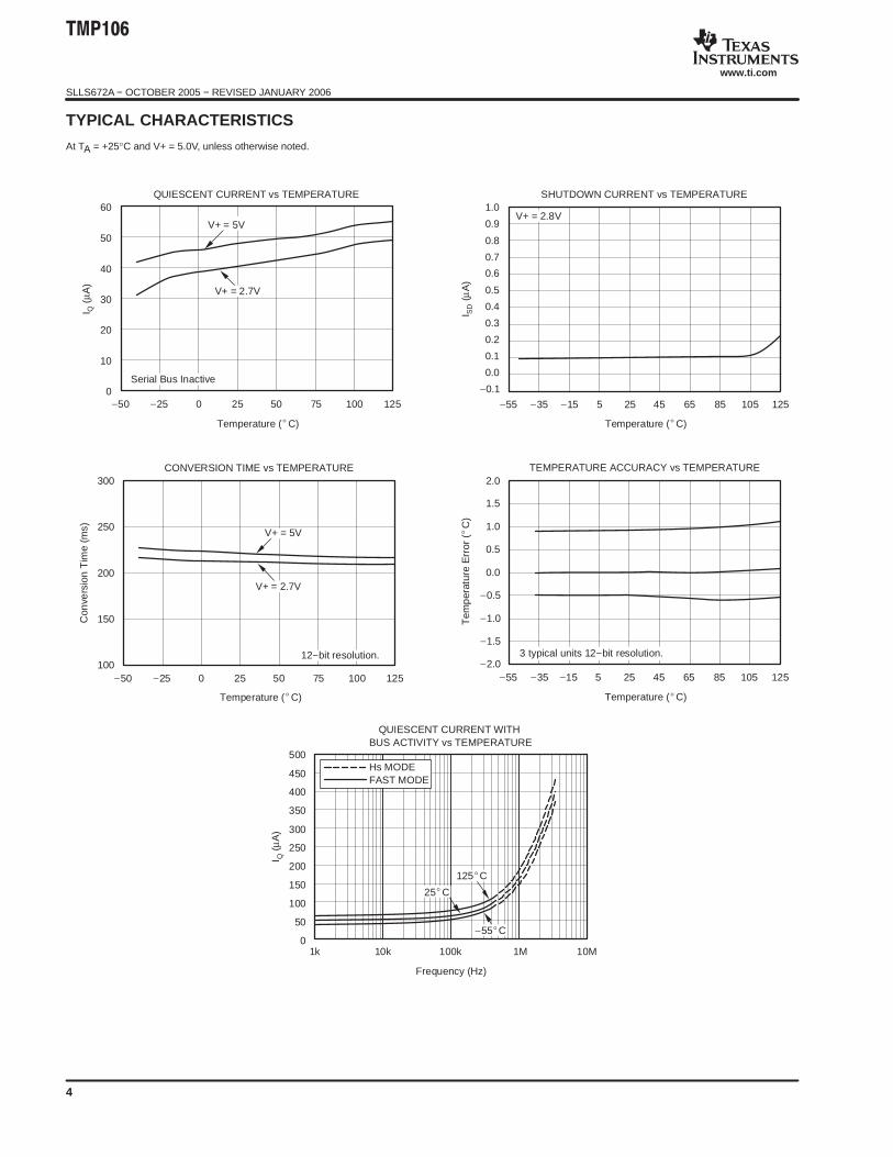
TYPICAL CHARACTERISTICS
At TA = +25°C and V+ = 5.0V, unless otherwise noted.
60
50
40
30
20
10
0
QUIESCENT CURRENT vs TEMPERATURE
Temperature (�C)
−50 −25 0 25 50 75 100 125
I Q(µ
A)
V+ = 2.7V
Serial Bus Inactive
V+ = 5V
300
250
200
150
100
CONVERSION TIME vs TEMPERATURE
Temperature (�C)
Con
vers
ion
Tim
e(m
s)
−50 −25 0 25 50 75 100 125
V+ = 2.7V
V+ = 5V
12−bit resolution.
1.0
0.9
0.8
0.7
0.6
0.5
0.4
0.3
0.2
0.1
0.0
−0.1
SHUTDOWN CURRENT vs TEMPERATURE
Temperature (�C)
I SD
(µA
)
−55 −35 −15 5 25 45 65 85 105 125
V+ = 2.8V
2.0
1.5
1.0
0.5
0.0
−0.5
−1.0
−1.5
−2.0
TEMPERATURE ACCURACY vs TEMPERATURET
emp
erat
ure
Err
or(�
C)
3 typical units 12−bit resolution.
Temperature (�C)
−55 −35 −15 5 25 45 65 85 105 125
500
450
400
350
300
250
200
150
100
50
0
QUIESCENT CURRENT WITHBUS ACTIVITY vs TEMPERATURE
Frequency (Hz)
1k 10k 100k 1M 10M
I Q(µ
A)
125�C
25�C
−55�C
Hs MODEFAST MODE
�"�#$%
SLLS672A − OCTOBER 2005 − REVISED JANUARY 2006
www.ti.com
5
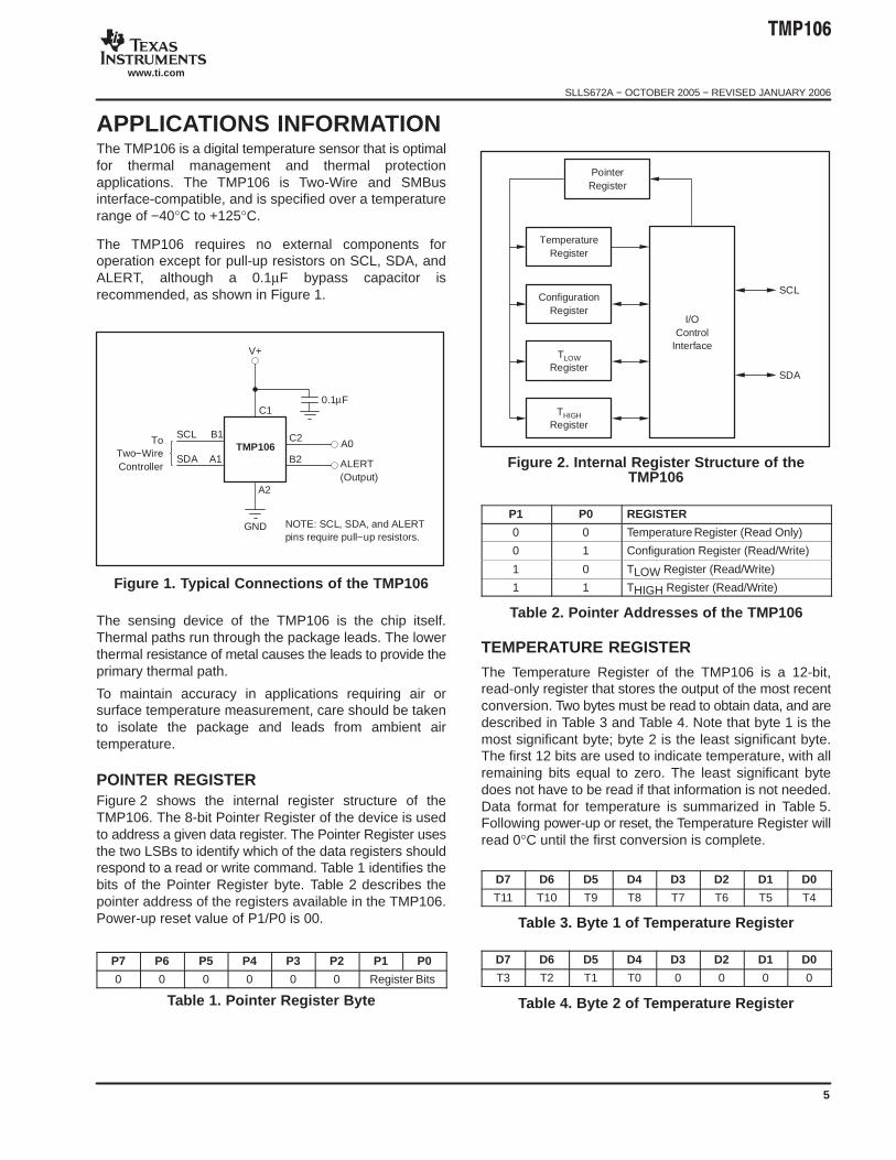
APPLICATIONS INFORMATIONThe TMP106 is a digital temperature sensor that is optimalfor thermal management and thermal protectionapplications. The TMP106 is Two-Wire and SMBusinterface-compatible, and is specified over a temperaturerange of −40°C to +125°C.
The TMP106 requires no external components foroperation except for pull-up resistors on SCL, SDA, andALERT, although a 0.1µF bypass capacitor isrecommended, as shown in Figure 1.
TMP106
0.1µF
V+
GND
A2
B2
C2
C1
ALERT(Output)
A0B1
A1
SCL
SDA
ToTwo−WireController
NOTE: SCL, SDA, and ALERTpins require pull−up resistors.
Figure 1. Typical Connections of the TMP106
The sensing device of the TMP106 is the chip itself.Thermal paths run through the package leads. The lowerthermal resistance of metal causes the leads to provide theprimary thermal path.
To maintain accuracy in applications requiring air orsurface temperature measurement, care should be takento isolate the package and leads from ambient airtemperature.
POINTER REGISTERFigure 2 shows the internal register structure of theTMP106. The 8-bit Pointer Register of the device is usedto address a given data register. The Pointer Register usesthe two LSBs to identify which of the data registers shouldrespond to a read or write command. Table 1 identifies thebits of the Pointer Register byte. Table 2 describes thepointer address of the registers available in the TMP106.Power-up reset value of P1/P0 is 00.
P7 P6 P5 P4 P3 P2 P1 P0
0 0 0 0 0 0 Register Bits
Table 1. Pointer Register Byte
I/OControl
Interface
SCL
SDA
TemperatureRegister
ConfigurationRegister
TLOWRegister
THIGHRegister
PointerRegister
Figure 2. Internal Register Structure of theTMP106
P1 P0 REGISTER
0 0 Temperature Register (Read Only)
0 1 Configuration Register (Read/Write)
1 0 TLOW Register (Read/Write)
1 1 THIGH Register (Read/Write)
Table 2. Pointer Addresses of the TMP106
TEMPERATURE REGISTER
The Temperature Register of the TMP106 is a 12-bit,read-only register that stores the output of the most recentconversion. Two bytes must be read to obtain data, and aredescribed in Table 3 and Table 4. Note that byte 1 is themost significant byte; byte 2 is the least significant byte.The first 12 bits are used to indicate temperature, with allremaining bits equal to zero. The least significant bytedoes not have to be read if that information is not needed.Data format for temperature is summarized in Table 5.Following power-up or reset, the Temperature Register willread 0°C until the first conversion is complete.
D7 D6 D5 D4 D3 D2 D1 D0
T11 T10 T9 T8 T7 T6 T5 T4
Table 3. Byte 1 of Temperature Register
D7 D6 D5 D4 D3 D2 D1 D0
T3 T2 T1 T0 0 0 0 0
Table 4. Byte 2 of Temperature Register

�"�#$%
SLLS672A − OCTOBER 2005 − REVISED JANUARY 2006
www.ti.com
6
TEMPERATURE(°C)
DIGITAL OUTPUT(BINARY) HEX
128 0111 1111 1111 7FF
127.9375 0111 1111 1111 7FF
100 0110 0100 0000 640
80 0101 0000 0000 500
75 0100 1011 0000 4B0
50 0011 0010 0000 320
25 0001 1001 0000 190
0.25 0000 0000 0100 004
0 0000 0000 0000 000
−0.25 1111 1111 1100 FFC
−25 1110 0111 0000 E70
−55 1100 1001 0000 C90
Table 5. Temperature Data Format
The user can obtain 9, 10, 11, or 12 bits of resolution byaddressing the Configuration Register and setting theresolution bits accordingly. For 9-, 10-, or 11-bit resolution,the most significant bits in the Temperature Register areused with the unused LSBs set to zero.
CONFIGURATION REGISTERThe Configuration Register is an 8-bit read/write registerused to store bits that control the operational modes of thetemperature sensor. Read/write operations are performedMSB first. The format of the Configuration Register for theTMP106 is shown in Table 6, followed by a breakdown ofthe register bits. The power-up/reset value of theConfiguration Register is all bits equal to 0.
BYTE D7 D6 D5 D4 D3 D2 D1 D0
1 OS R1 R0 F1 F0 POL TM SD
Table 6. Configuration Register Format
SHUTDOWN MODE (SD)The Shutdown Mode of the TMP106 allows the user tosave maximum power by shutting down all device circuitryother than the serial interface, which reduces currentconsumption to typically less than 0.1µA. Shutdown Modeis enabled when the SD bit is 1; the device will shut downonce the current conversion is completed. When SD isequal to 0, the device will maintain a continuousconversion state.
THERMOSTAT MODE (TM)The Thermostat Mode bit of the TMP106 indicates to thedevice whether to operate in Comparator Mode (TM = 0)or Interrupt Mode (TM = 1). For more information oncomparator and interrupt modes, see the High and LowLimit Registers section.
POLARITY (POL)The Polarity Bit of the TMP106 allows the user to adjust thepolarity of the ALERT pin output. If POL = 0, the ALERT pinwill be active LOW, as shown in Figure 3. For POL = 1, theALERT pin will be active HIGH, and the state of the ALERTpin is inverted.
MeasuredTemperature
THIGH
TLOW
TMP106 ALERT PIN(Comparator Mode)
POL = 0
TMP106 ALERT PIN(Interrupt Mode)
POL = 0
TMP106 ALERT PIN(Comparator Mode)
POL = 1
TMP106 ALERT PIN(Interrupt Mode)
POL = 1
Read Read
Time
Read
Figure 3. Output Transfer Function Diagrams
FAULT QUEUE (F1/F0)A fault condition is defined as when the measuredtemperature exceeds the user-defined limits set in theTHIGH and TLOW Registers. Additionally, the number offault conditions required to generate an alert may beprogrammed using the fault queue. The fault queue isprovided to prevent a false alert as a result ofenvironmental noise. The fault queue requiresconsecutive fault measurements in order to trigger thealert function. Table 7 defines the number of measuredfaults that may be programmed to trigger an alert conditionin the device. For THIGH and TLOW register format and byteorder, see the High and Low Limit Registers section.
F1 F0 CONSECUTIVE FAULTS
0 0 1
0 1 2
1 0 4
1 1 6
Table 7. Fault Settings of the TMP106
�"�#$%
SLLS672A − OCTOBER 2005 − REVISED JANUARY 2006
www.ti.com
7
CONVERTER RESOLUTION (R1/R0)The Converter Resolution bits control the resolution of theinternal analog-to-digital (A/D) converter. This controlallows the user to maximize efficiency by programming forhigher resolution or faster conversion time. Table 8identifies the resolution bits and the relationship betweenresolution and conversion time.
R1 R0 RESOLUTIONCONVERSION TIME
(typical)
0 0 9 Bits (0.5°C) 27.5ms
0 1 10 Bits (0.25°C) 55ms
1 0 11 Bits (0.125°C) 110ms
1 1 12 Bits (0.0625°C) 220ms
Table 8. Resolution of the TMP106
ONE-SHOT (OS)The TMP106 features a One-Shot TemperatureMeasurement Mode. When the device is in ShutdownMode, writing a ‘1’ to the OS bit starts a single temperatureconversion. The device will return to the shutdown state atthe completion of the single conversion. This option isuseful to reduce power consumption in the TMP106 whencontinuous temperature monitoring is not required. Whenthe Configuration Register is read, the OS always readszero.
HIGH AND LOW LIMIT REGISTERSIn Comparator Mode (TM = 0), the ALERT pin of theTMP106 becomes active when the temperature equals orexceeds the value in THIGH and generates a consecutivenumber of faults according to fault bits F1 and F0. TheALERT pin remains active until the temperature falls belowthe indicated TLOW value for the same number of faults.
In Interrupt Mode (TM = 1), the ALERT pin becomes activewhen the temperature equals or exceeds THIGH for aconsecutive number of fault conditions. The ALERT pinremains active until a read operation of any registeroccurs, or until the device successfully responds to theSMBus Alert Response address. The ALERT pin clears ifthe device is placed in Shutdown Mode. Once the ALERTpin is cleared, it will only become active again by thetemperature falling below TLOW. When the temperaturefalls below TLOW, the ALERT pin becomes active andremains active until cleared by a read operation of anyregister or a successful response to the SMBus Alert
Response address. When the ALERT pin clears, theabove cycle will repeat, with the ALERT pin becomingactive when the temperature equals or exceeds THIGH.The ALERT pin can also be cleared by resetting the devicewith the General Call Reset command. This reset alsoclears the state of the internal registers in the device,returning the device to Comparator Mode (TM = 0).
Both operational modes are represented in Figure 3.Table 9 and Table 10 describe the format for the THIGH andTLOW Registers. Note that the most significant byte is sentfirst, followed by the least significant byte. Power-up resetvalues for THIGH and TLOW are:
THIGH = 80°C and TLOW = 75°C
The format of the data for THIGH and TLOW is the same asfor the Temperature Register.
BYTE D7 D6 D5 D4 D3 D2 D1 D0
1 H11 H10 H9 H8 H7 H6 H5 H4
BYTE D7 D6 D5 D4 D3 D2 D1 D0
2 H3 H2 H1 H0 0 0 0 0
Table 9. Bytes 1 and 2 of T HIGH Register
BYTE D7 D6 D5 D4 D3 D2 D1 D0
1 L11 L10 L9 L8 L7 L6 L5 L4
BYTE D7 D6 D5 D4 D3 D2 D1 D0
2 L3 L2 L1 L0 0 0 0 0
Table 10. Bytes 1 and 2 of T LOW Register
All 12 bits for the Temperature, THIGH, and TLOW Registersare used in the comparisons for the ALERT function for allconverter resolutions. The three LSBs in THIGH and TLOWcan affect the ALERT output even if the converter isconfigured for 9-bit resolution.
SERIAL INTERFACEThe TMP106 operates only as a slave device on theTwo-Wire bus and SMBus. Connections to the bus aremade via the open-drain I/O lines SDA and SCL. The SDAand SCL pins feature integrated spike suppression filtersand Schmitt triggers to minimize the effects of input spikesand bus noise. The TMP106 supports the transmissionprotocol for fast (1kHz to 400kHz) and high-speed (1kHzto 3.4MHz) modes. All data bytes are transmitted MSBfirst.

�"�#$%
SLLS672A − OCTOBER 2005 − REVISED JANUARY 2006
www.ti.com
8
SERIAL BUS ADDRESSTo communicate with the TMP106, the master must firstaddress slave devices via a slave address byte. The slaveaddress byte consists of seven address bits, and adirection bit indicating the intent of executing a read orwrite operation.
The TMP106 features one address pin allowing up to twodevices to be connected per bus. Pin logic levels aredescribed in Table 11. The address pin of the TMP106 isread after reset, at start of communication, or in responseto a Two-Wire address acquire request. Following thereading of the pin state, the address is latched to minimizepower dissipation associated with detection.
A0 SLAVE ADDRESS
0 1001000
1 1001001
Table 11. Address Pin and Slave Addresses forthe TMP106
BUS OVERVIEWThe device that initiates the transfer is called a master, andthe devices controlled by the master are slaves. The busmust be controlled by a master device that generates theserial clock (SCL), controls the bus access, and generatesthe START and STOP conditions.
To address a specific device, a START condition isinitiated, indicated by pulling the data-line (SDA) from aHIGH to LOW logic level while SCL is HIGH. All slaves onthe bus shift in the slave address byte, with the last bitindicating whether a read or write operation is intended.During the ninth clock pulse, the slave being addressedresponds to the master by generating an Acknowledgeand pulling SDA LOW.
Data transfer is then initiated and sent over eight clockpulses followed by an Acknowledge Bit. During datatransfer SDA must remain stable while SCL is HIGH, asany change in SDA while SCL is HIGH will be interpretedas a control signal.
Once all data has been transferred, the master generatesa STOP condition, indicated by pulling SDA from LOW toHIGH while SCL is HIGH.
WRITING/READING TO THE TMP106Accessing a particular register on the TMP106 isaccomplished by writing the appropriate value to thePointer Register. The value for the Pointer Register is thefirst byte transferred after the slave address byte with theR/W bit LOW. Every write operation to the TMP106requires a value for the Pointer Register. (Refer toFigure 5.)
When reading from the TMP106, the last value stored inthe Pointer Register by a write operation is used todetermine which register is read by a read operation. Tochange the register pointer for a read operation, a newvalue must be written to the Pointer Register. This isaccomplished by issuing a slave address byte with theR/W bit LOW, followed by the Pointer Register byte. Noadditional data are required. The master can thengenerate a START condition and send the slave addressbyte with the R/W bit HIGH to initiate the read command.See Figure 6 for details of this sequence. If repeated readsfrom the same register are desired, it is not necessary tocontinually send the Pointer Register byte, as the TMP106remembers the Pointer Register value until it is changedby the next write operation.
Note that register bytes are sent most-significant byte first,followed by the least-significant byte.

�"�#$%
SLLS672A − OCTOBER 2005 − REVISED JANUARY 2006
www.ti.com
9
SLAVE MODE OPERATIONSThe TMP106 can operate as a slave receiver or slavetransmitter.
Slave Receiver Mode:The first byte transmitted by the master is the slaveaddress, with the R/W bit LOW. The TMP106 thenacknowledges reception of a valid address. The next bytetransmitted by the master is the Pointer Register. TheTMP106 then acknowledges reception of the PointerRegister byte. The next byte or bytes are written to theregister addressed by the Pointer Register. The TMP106acknowledges reception of each data byte. The mastermay terminate data transfer by generating a START orSTOP condition.
Slave Transmitter Mode:The first byte is transmitted by the master and is the slaveaddress, with the R/W bit HIGH. The slave acknowledgesreception of a valid slave address. The next byte istransmitted by the slave and is the most significant byte ofthe register indicated by the Pointer Register. The masteracknowledges reception of the data byte. The next bytetransmitted by the slave is the least significant byte. Themaster acknowledges reception of the data byte. Themaster may terminate data transfer by generating aNot-Acknowledge on reception of any data byte, orgenerating a START or STOP condition.
SMBus ALERT FUNCTIONThe TMP106 supports the SMBus Alert function. Whenthe TMP106 is operating in Interrupt Mode (TM = 1), theALERT pin of the TMP106 may be connected as anSMBus Alert signal. When a master senses that an ALERTcondition is present on the ALERT line, the master sendsan SMBus Alert command (00011001) on the bus. If theALERT pin of the TMP106 is active, the devices willacknowledge the SMBus Alert command and respond byreturning its slave address on the SDA line. The eighth bit(LSB) of the slave address byte will indicate if thetemperature exceeding THIGH or falling below TLOWcaused the ALERT condition. This bit will be HIGH if thetemperature is greater than or equal to THIGH. This bit willbe LOW if the temperature is less than TLOW. Refer toFigure 7 for details of this sequence.
If multiple devices on the bus respond to the SMBus Alertcommand, arbitration during the slave address portion ofthe SMBus Alert command will determine which devicewill clear its ALERT status. If the TMP106 wins thearbitration, its ALERT pin will become inactive at thecompletion of the SMBus Alert command. If the TMP106loses the arbitration, its ALERT pin will remain active.
GENERAL CALLThe TMP106 responds to a Two-Wire General Calladdress (0000000) if the eighth bit is 0. The device willacknowledge the General Call address and respond tocommands in the second byte. If the second byte is00000100, the TMP106 will latch the status of the addresspin, but will not reset. If the second byte is 00000110, theTMP106 will latch the status of the address pin and resetthe internal registers to their power-up values.
HIGH-SPEED MODEIn order for the Two-Wire bus to operate at frequenciesabove 400kHz, the master device must issue an Hs-modemaster code (00001XXX) as the first byte after a STARTcondition to switch the bus to high-speed operation. TheTMP106 will not acknowledge this byte, but will switch itsinput filters on SDA and SCL and its output filters on SDAto operate in Hs-mode, allowing transfers at up to 3.4MHz.After the Hs-mode master code has been issued, themaster will transmit a Two-Wire slave address to initiate adata transfer operation. The bus will continue to operate inHs-mode until a STOP condition occurs on the bus. Uponreceiving the STOP condition, the TMP106 will switch theinput and output filters back to fast-mode operation.
TIMEOUT FUNCTIONThe TMP106 will reset the serial interface if either SCL orSDA are held LOW for 54ms (typ) between a START andSTOP condition. The TMP106 will release the bus if it ispulled LOW and will wait for a START condition. To avoidactivating the timeout function, it is necessary to maintaina communication speed of at least 1kHz for SCL operatingfrequency.
�"�#$%
SLLS672A − OCTOBER 2005 − REVISED JANUARY 2006
www.ti.com
10
TIMING DIAGRAMSThe TMP106 is Two-Wire- and SMBus-compatible.Figure 4 to Figure 7 describe the various operations on theTMP106. Bus definitions are given below. Parameters forFigure 4 are defined in Table 12.
Bus Idle: Both SDA and SCL lines remain HIGH.
Start Data Transfer: A change in the state of the SDA line,from HIGH to LOW, while the SCL line is HIGH, defines aSTART condition. Each data transfer is initiated with aSTART condition.
Stop Data Transfer: A change in the state of the SDA linefrom LOW to HIGH while the SCL line is HIGH defines aSTOP condition. Each data transfer is terminated with arepeated START or STOP condition.
Data Transfer: The number of data bytes transferredbetween a START and a STOP condition is not limited andis determined by the master device. The receiveracknowledges the transfer of data.
Acknowledge: Each receiving device, when addressed,is obliged to generate an Acknowledge bit. A device thatacknowledges must pull down the SDA line during theAcknowledge clock pulse in such a way that the SDA lineis stable LOW during the HIGH period of the Acknowledgeclock pulse. Setup and hold times must be taken intoaccount. On a master receive, the termination of the datatransfer can be signaled by the master generating aNot-Acknowledge on the last byte that has beentransmitted by the slave.
PARAMETERFAST MODE HIGH-SPEED MODE
UNITSPARAMETERMIN MAX MIN MAX
UNITS
SCL Operating Frequency f(SCL) 0.001 0.4 0.001 3.4 MHz
Bus Free Time Between STOP and START Condition t(BUF) 600 160 ns
Hold time after repeated START condition.After this period, the first clock is generated.
t(HDSTA) 100 100 ns
Repeated START Condition Setup Time t(SUSTA) 100 100 ns
STOP Condition Setup Time t(SUSTO) 100 100 ns
Data Hold Time t(HDDAT) 0 0 ns
Data Setup Time t(SUDAT) 100 10 ns
SCL Clock LOW Period t(LOW) 1300 160 ns
SCL Clock HIGH Period t(HIGH) 600 60 ns
Clock/Data Fall Time tF 300 160 ns
Clock/Data Rise TimetR
300 160 nsfor SCLK ≤ 100kHz
tR 1000 ns
Table 12. Timing Diagram Definitions for the TMP106
TWO-WIRE TIMING DIAGRAMS
SCL
SDA
t(LOW)tR tF t(HDSTA)
t(HDSTA)
t(HDDAT)
t(BUF)
t(SUDAT)
t(HIGH) t(SUSTA)t(SUSTO)
P S S P
Figure 4. Two-Wire Timing Diagram

�"�#$%
SLLS672A − OCTOBER 2005 − REVISED JANUARY 2006
www.ti.com
11
Frame 1 Two−Wire Slave Address Byte Frame 2 Pointer Register Byte
Frame 4 Data Byte 2
1
Start ByMaster
ACK ByTMP106
ACK ByTMP106
ACK ByTMP106
Stop ByMaster
1 9 1
1
D7 D6 D5 D4 D3 D2 D1 D0
9
Frame 3 Data Byte 1
ACK ByTMP106
1
D7SDA(Continued)
SCL(Continued)
D6 D5 D4 D3 D2 D1 D0
9
9
SDA
SCL
0 0 1 0 0 A0 R/W 0 0 0 0 0 0 P1 P0 …
…
Figure 5. Two-Wire Timing Diagram for TMP106 Write Word Format
Frame 1 Two−Wire Slave Address Byte Frame 2 Pointer Register Byte
1
Start ByMaster
ACK ByTMP106
ACK ByTMP106
Frame 3 Two−Wire Slave Address Byte Frame 4 Data Byte 1 Read Register
Start ByMaster
ACK ByTMP106
ACK ByMaster
FromTMP106
1 9 1 9
1 9 1 9
SDA
SCL
0 0 R/W 0 0 0 0 0 0 P1 P0 …
…
…
…
SDA(Continued)
SCL(Continued)
SDA(Continued)
SCL(Continued)
1 0 0 1
0 0 A0
0 0 A0 R/W D7 D6 D5 D4 D3 D2 D1 D0
Frame 5 Data Byte 2 Read Register
Stop ByMaster
ACK ByMaster
FromTMP106
1 9
D7 D6 D5 D4 D3 D2 D1 D0
Figure 6. Two-Wire Timing Diagram for Read Word Format

�"�#$%
SLLS672A − OCTOBER 2005 − REVISED JANUARY 2006
www.ti.com
12
Frame 1 SMBus ALERT Response Address Byte Frame 2 Slave Address Byte
Start ByMaster
ACK ByTMP106
FromTMP106
NACK ByMaster
Stop ByMaster
1 9 1 9
SDA
SCL
ALERT
0 0 0 1 1 0 0 R/W 1 0 0 1 0 0 A0 Status
Figure 7. Timing Diagram for SMBus ALERT
13

PACKAGE OPTION ADDENDUM
www.ti.com 10-Dec-2020
Addendum-Page 1
PACKAGING INFORMATION
Orderable Device Status(1)
Package Type PackageDrawing
Pins PackageQty
Eco Plan(2)
Lead finish/Ball material
(6)
MSL Peak Temp(3)
Op Temp (°C) Device Marking(4/5)
Samples
TMP106YZCR ACTIVE DSBGA YZC 6 3000 RoHS & Green SNAGCU Level-1-260C-UNLIM -40 to 125 F7
TMP106YZCT ACTIVE DSBGA YZC 6 250 RoHS & Green SNAGCU Level-1-260C-UNLIM -40 to 125 F7
(1) The marketing status values are defined as follows:ACTIVE: Product device recommended for new designs.LIFEBUY: TI has announced that the device will be discontinued, and a lifetime-buy period is in effect.NRND: Not recommended for new designs. Device is in production to support existing customers, but TI does not recommend using this part in a new design.PREVIEW: Device has been announced but is not in production. Samples may or may not be available.OBSOLETE: TI has discontinued the production of the device.
(2) RoHS: TI defines "RoHS" to mean semiconductor products that are compliant with the current EU RoHS requirements for all 10 RoHS substances, including the requirement that RoHS substancedo not exceed 0.1% by weight in homogeneous materials. Where designed to be soldered at high temperatures, "RoHS" products are suitable for use in specified lead-free processes. TI mayreference these types of products as "Pb-Free".RoHS Exempt: TI defines "RoHS Exempt" to mean products that contain lead but are compliant with EU RoHS pursuant to a specific EU RoHS exemption.Green: TI defines "Green" to mean the content of Chlorine (Cl) and Bromine (Br) based flame retardants meet JS709B low halogen requirements of <=1000ppm threshold. Antimony trioxide basedflame retardants must also meet the <=1000ppm threshold requirement.
(3) MSL, Peak Temp. - The Moisture Sensitivity Level rating according to the JEDEC industry standard classifications, and peak solder temperature.
(4) There may be additional marking, which relates to the logo, the lot trace code information, or the environmental category on the device.
(5) Multiple Device Markings will be inside parentheses. Only one Device Marking contained in parentheses and separated by a "~" will appear on a device. If a line is indented then it is a continuationof the previous line and the two combined represent the entire Device Marking for that device.
(6) Lead finish/Ball material - Orderable Devices may have multiple material finish options. Finish options are separated by a vertical ruled line. Lead finish/Ball material values may wrap to twolines if the finish value exceeds the maximum column width.
Important Information and Disclaimer:The information provided on this page represents TI's knowledge and belief as of the date that it is provided. TI bases its knowledge and belief on informationprovided by third parties, and makes no representation or warranty as to the accuracy of such information. Efforts are underway to better integrate information from third parties. TI has taken andcontinues to take reasonable steps to provide representative and accurate information but may not have conducted destructive testing or chemical analysis on incoming materials and chemicals.TI and TI suppliers consider certain information to be proprietary, and thus CAS numbers and other limited information may not be available for release.
In no event shall TI's liability arising out of such information exceed the total purchase price of the TI part(s) at issue in this document sold by TI to Customer on an annual basis.

PACKAGE OPTION ADDENDUM
www.ti.com 10-Dec-2020
Addendum-Page 2
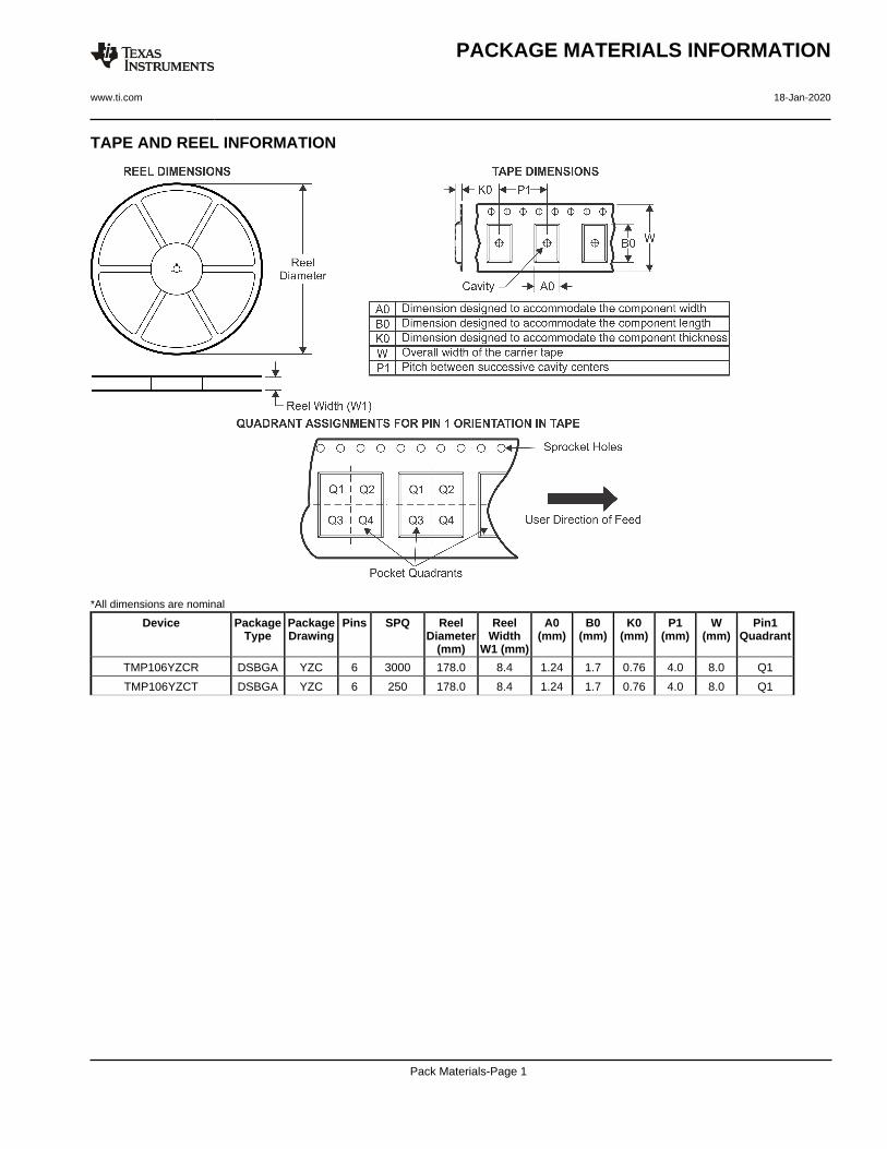
TAPE AND REEL INFORMATION
*All dimensions are nominal
Device PackageType
PackageDrawing
Pins SPQ ReelDiameter
(mm)
ReelWidth
W1 (mm)
A0(mm)
B0(mm)
K0(mm)
P1(mm)
W(mm)
Pin1Quadrant
TMP106YZCR DSBGA YZC 6 3000 178.0 8.4 1.24 1.7 0.76 4.0 8.0 Q1
TMP106YZCT DSBGA YZC 6 250 178.0 8.4 1.24 1.7 0.76 4.0 8.0 Q1
PACKAGE MATERIALS INFORMATION
www.ti.com 18-Jan-2020
Pack Materials-Page 1

*All dimensions are nominal
Device Package Type Package Drawing Pins SPQ Length (mm) Width (mm) Height (mm)
TMP106YZCR DSBGA YZC 6 3000 220.0 220.0 35.0
TMP106YZCT DSBGA YZC 6 250 220.0 220.0 35.0
PACKAGE MATERIALS INFORMATION
www.ti.com 18-Jan-2020
Pack Materials-Page 2

www.ti.com
PACKAGE OUTLINE
C0.625 MAX
0.350.15
1TYP
0.25 TYP
6X 0.350.25
0.5TYP
0.5 TYP
B E A
D
4219522/A 02/2015
DSBGA - 0.625 mm max heightYZC0006DIE SIZE BALL GRID ARRAY
NOTES: 1. All linear dimensions are in millimeters. Any dimensions in parenthesis are for reference only. Dimensioning and tolerancing per ASME Y14.5M.2. This drawing is subject to change without notice.3. NanoFreeTM package configuration.
NanoFree Is a trademark of Texas Instruments.
BALL A1CORNER
SEATING PLANE
BALL TYP 0.08 C
A
1
0.015 C A B
SYMM
SYMM
C
2
B
SCALE 9.000

www.ti.com
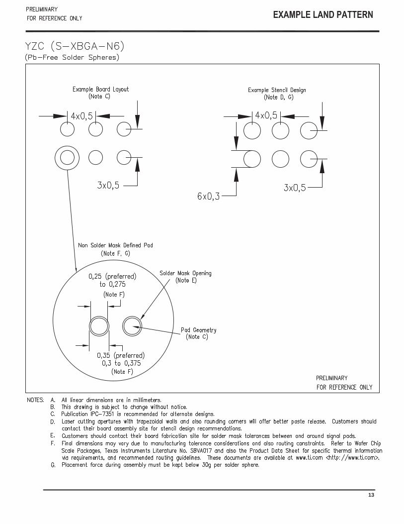
EXAMPLE BOARD LAYOUT
6X ( )0.265(0.5) TYP
(0.5) TYP
( )METAL0.265 0.05 MAX
SOLDER MASKOPENING
METALUNDERSOLDER MASK
( )SOLDER MASKOPENING
0.265
0.05 MIN
4219522/A 02/2015
DSBGA - 0.625 mm max heightYZC0006DIE SIZE BALL GRID ARRAY
NOTES: (continued) 4. Final dimensions may vary due to manufacturing tolerance considerations and also routing constraints. For more information, see Texas Instruments literature number SNVA009 (www.ti.com/lit/snva009).
SYMM
SYMM
LAND PATTERN EXAMPLESCALE:30X
1 2A
B
C
NON-SOLDER MASKDEFINED
(PREFERRED)
SOLDER MASK DETAILSNOT TO SCALE
SOLDER MASKDEFINED

www.ti.com
EXAMPLE STENCIL DESIGN
(0.5)TYP
(0.5) TYP
6X ( 0.25)(R ) TYP0.05
METALTYP
4219522/A 02/2015
DSBGA - 0.625 mm max heightYZC0006DIE SIZE BALL GRID ARRAY
NOTES: (continued) 5. Laser cutting apertures with trapezoidal walls and rounded corners may offer better paste release.
SYMM
SYMM
SOLDER PASTE EXAMPLEBASED ON 0.1 mm THICK STENCIL
SCALE:40X
1 2
A
B
C

IMPORTANT NOTICE AND DISCLAIMERTI PROVIDES TECHNICAL AND RELIABILITY DATA (INCLUDING DATA SHEETS), DESIGN RESOURCES (INCLUDING REFERENCE DESIGNS), APPLICATION OR OTHER DESIGN ADVICE, WEB TOOLS, SAFETY INFORMATION, AND OTHER RESOURCES “AS IS” AND WITH ALL FAULTS, AND DISCLAIMS ALL WARRANTIES, EXPRESS AND IMPLIED, INCLUDING WITHOUT LIMITATION ANY IMPLIED WARRANTIES OF MERCHANTABILITY, FITNESS FOR A PARTICULAR PURPOSE OR NON-INFRINGEMENT OF THIRD PARTY INTELLECTUAL PROPERTY RIGHTS.These resources are intended for skilled developers designing with TI products. You are solely responsible for (1) selecting the appropriate TI products for your application, (2) designing, validating and testing your application, and (3) ensuring your application meets applicable standards, and any other safety, security, regulatory or other requirements.These resources are subject to change without notice. TI grants you permission to use these resources only for development of an application that uses the TI products described in the resource. Other reproduction and display of these resources is prohibited. No license is granted to any other TI intellectual property right or to any third party intellectual property right. TI disclaims responsibility for, and you will fully indemnify TI and its representatives against, any claims, damages, costs, losses, and liabilities arising out of your use of these resources.TI’s products are provided subject to TI’s Terms of Sale or other applicable terms available either on ti.com or provided in conjunction with such TI products. TI’s provision of these resources does not expand or otherwise alter TI’s applicable warranties or warranty disclaimers for TI products.TI objects to and rejects any additional or different terms you may have proposed. IMPORTANT NOTICE
Mailing Address: Texas Instruments, Post Office Box 655303, Dallas, Texas 75265Copyright © 2021, Texas Instruments Incorporated