digitally controlled oscillator (dco)-based architecture...
TRANSCRIPT

IEEE TRANSACTIONS ON CIRCUITS AND SYSTEMS—II: ANALOG AND DIGITAL SIGNAL PROCESSING, VOL. 50, NO. 11, NOVEMBER 2003 815
Digitally Controlled Oscillator (DCO)-BasedArchitecture for RF Frequency Synthesis in a
Deep-Submicrometer CMOS ProcessRobert Bogdan Staszewski, Member, IEEE, Dirk Leipold, Khurram Muhammad, and
Poras T. Balsara, Senior Member, IEEE
Abstract—A novel digitally controlled oscillator (DCO)-basedarchitecture for frequency synthesis in wireless RF applicationsis proposed and demonstrated. It deliberately avoids any use ofan analog tuning voltage control line. Fine frequency resolution isachieved through high-speed�� dithering. Other imperfectionsof analog circuits are compensated through digital means. The pre-sented ideas enable the employment of fully-digital frequency syn-thesizers using sophisticated signal processing algorithms, realizedin the most advanced deep-submicrometer digital CMOS processeswhich allow almost no analog extensions. They also promote cost-effective integration with the digital back-end onto a single silicondie. The demonstrator test chip has been fabricated in a digital0.13- m CMOS process together with a DSP, which acts as a digitalbaseband processor with a large number of digital gates in orderto investigate noise coupling. The phase noise is112 dBc/Hz at500-kHz offset. The close-in spurious tones are below 62 dBc,while the far-out spurs are below 80 dBc. The presented ideashave been incorporated in a commercial Bluetooth transceiver.
Index Terms—Deep-submicrometer CMOS, digital compen-sation, digital control, digitally controlled oscillator (DCO),frequency synthesizer.
I. INTRODUCTION
T RADITIONAL designs of commercial frequency synthe-sizers for multigigahertz mobile RF wireless applications
have almost exclusively employed the use of a charge-pumpphase-locked loop(PLL), which acts as alocal oscillator(LO)for both a transmitter and a receiver. Unfortunately, the designflow and circuit techniques required are analog intensive andutilize process technologies that are incompatible with adigitalbaseband(DBB). Nowadays, the DBB design constantly mi-grates to the most advanced deep-submicrometer digital CMOSprocess available, which usually does not offer any analog ex-tensions and has very limited voltage headroom. Consequently,the aggressive cost and power reductions of high-volume mo-bile wireless solutions can only be realistically achieved by thehighest level of integration, and this favors digitally-intensiveapproach in the most aggressive deep-submicrometer process.
Deep-submicrometer CMOS processes present new integra-tion opportunities on one hand, but make it extremely difficultto implement traditional analog circuits, on the other. For
Manuscript received May 11, 2003; revised July 2003. This paper was rec-ommended by Guest Editor M. Perrott.
R. B. Staszewski, D. Leipold, and K. Muhammad are with the Texas Instru-ments Inc., Dallas, TX 75243 USA (e-mail: [email protected]).
P. T. Balsara is with the Center for Circuits and Systems, University of Texasat Dallas, Richardson, TX 75083 USA.
Digital Object Identifier 10.1109/TCSII.2003.819128
example, frequency tuning of a low-voltage deep-submicrom-eter CMOS oscillator is an extremely challenging task due toits highly nonlinear frequency versus voltage characteristics[1] and low-voltage headroom making it susceptible to thepower/ground supply and substrate noise. In such low supplyvoltage case, not only the dynamic range of the signal suffersbut also the noise floor rises, thus causing even more severedegradation of the signal-to-noise ratio. At times, it is possibleto find a specific solution, such as utilizing a voltage doubler[2]. Unfortunately, with each CMOS feature size reduction,the supply voltage needs also to be scaled down, which isinevitable in order to avoid breakdown and reliability issues.Circuits designed to ensure proper operation of RF amplifiers,filters, mixers, and oscillators depend on circuit techniquesthat operate best with long-channel, thick-oxide devices withsupply voltage of 2.5 V or higher. The process utilized inthis paper is optimized for short-channel, thin-oxide devicesoperating as digital switches at only 1.5 V. In order to addressthe various deep-submicrometer RF integration issues forfrequency synthesis, digitally-intensive techniques need to bedeveloped such that analog imperfections are compensated forby using advanced signal processing techniques.
So far there have not been any reports in literature (exceptrecently in [1]) on thefully digital control of oscillators forRF applications. Lack of the fully digital control is a severeimpediment for the total integration in a deep-submicrometerCMOS process, without which signal processing algorithmscannot be used to control or drive the analog circuits. Therehave been several disclosures on ring-oscillator-based DCOsfor clock recovery and clock generation applications [3] [4].However, the frequency resolution is low and spurious tonelevel is high for these DCOs, which seem to become an effectivedeterrent against digitally-intensive RF synthesizers for wire-less communications. DCO in reference [1] deliberately avoidsany analog tuning voltage controls. This allows for its loopcontrol circuitry, including loop filter, to be implemented in afully digital manner. That DCO, however, provides only a rawand bare minimum of functionality from a signal processingstandpoint. This paper introduces a circuitry built around itfor the purpose of adding a hierarchical layer of arithmeticabstraction that makes it easier to operate the DCO from higherlogical levels in a wide variety of digitally-intensive synthesizerarchitectures.
The organization of this paper is as follows. Section II givesan overview of the digitally controlled oscillator, whose time-
1057-7130/03$17.00 © 2003 IEEE
816 IEEE TRANSACTIONS ON CIRCUITS AND SYSTEMS—II: ANALOG AND DIGITAL SIGNAL PROCESSING, VOL. 50, NO. 11, NOVEMBER 2003
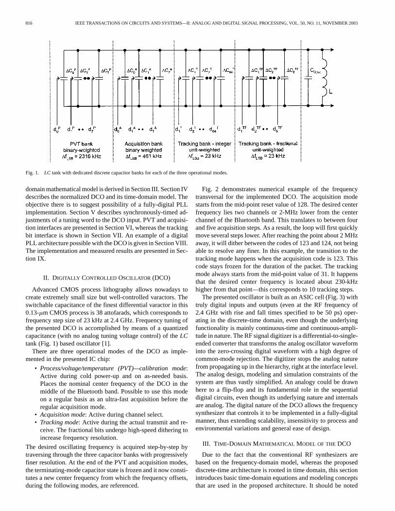
Fig. 1. LC tank with dedicated discrete capacitor banks for each of the three operational modes.
domain mathematical model is derived in Section III. Section IVdescribes the normalized DCO and its time-domain model. Theobjective there is to suggest possibility of a fully-digital PLLimplementation. Section V describes synchronously-timed ad-justments of a tuning word to the DCO input. PVT and acquisi-tion interfaces are presented in Section VI, whereas the trackingbit interface is shown in Section VII. An example of a digitalPLL architecture possible with the DCO is given in Section VIII.The implementation and measured results are presented in Sec-tion IX.
II. DIGITALLY CONTROLLED OSCILLATOR (DCO)
Advanced CMOS process lithography allows nowadays tocreate extremely small size but well-controlled varactors. Theswitchable capacitance of the finest differential varactor in this0.13- m CMOS process is 38 attofarads, which corresponds tofrequency step size of 23 kHz at 2.4 GHz. Frequency tuning ofthe presented DCO is accomplished by means of a quantizedcapacitance (with no analog tuning voltage control) of theLCtank (Fig. 1) based oscillator [1].
There are three operational modes of the DCO as imple-mented in the presented IC chip:
• Process/voltage/temperature (PVT)—calibration mode:Active during cold power-up and on as-needed basis.Places the nominal center frequency of the DCO in themiddle of the Bluetooth band. Possible to use this modeon a regular basis as an ultra-fast acquisition before theregular acquisition mode.
• Acquisition mode: Active during channel select.• Tracking mode: Active during the actual transmit and re-
ceive. The fractional bits undergo high-speed dithering toincrease frequency resolution.
The desired oscillating frequency is acquired step-by-step bytraversing through the three capacitor banks with progressivelyfiner resolution. At the end of the PVT and acquisition modes,the terminating-mode capacitor state is frozen and it now consti-tutes a new center frequency from which the frequency offsets,during the following modes, are referenced.
Fig. 2 demonstrates numerical example of the frequencytransversal for the implemented DCO. The acquisition modestarts from the mid-point reset value of 128. The desired centerfrequency lies two channels or 2-MHz lower from the centerchannel of the Bluetooth band. This translates to between fourand five acquisition steps. As a result, the loop will first quicklymove several steps lower. After reaching the point about 2 MHzaway, it will dither between the codes of 123 and 124, not beingable to resolve any finer. In this example, the transition to thetracking mode happens when the acquisition code is 123. Thiscode stays frozen for the duration of the packet. The trackingmode always starts from the mid-point value of 31. It happensthat the desired center frequency is located about 230-kHzhigher from that point—this corresponds to 10 tracking steps.
The presented oscillator is built as an ASIC cell (Fig. 3) withtruly digital inputs and outputs (even at the RF frequency of2.4 GHz with rise and fall times specified to be 50 ps) oper-ating in the discrete-time domain, even though the underlyingfunctionality is mainly continuous-time and continuous-ampli-tude in nature. The RF signal digitizer is a differential-to-single-ended converter that transforms the analog oscillator waveforminto the zero-crossing digital waveform with a high degree ofcommon-mode rejection. The digitizer stops the analog naturefrom propagating up in the hierarchy, right at the interface level.The analog design, modeling and simulation constraints of thesystem are thus vastly simplified. An analogy could be drawnhere to a flip-flop and its fundamental role in the sequentialdigital circuits, even though its underlying nature and internalsare analog. The digital nature of the DCO allows the frequencysynthesizer that controls it to be implemented in a fully-digitalmanner, thus extending scalability, insensitivity to process andenvironmental variations and general ease of design.
III. T IME-DOMAIN MATHEMATICAL MODEL OF THEDCO
Due to the fact that the conventional RF synthesizers arebased on the frequency-domain model, whereas the proposeddiscrete-time architecture is rooted in time domain, this sectionintroduces basic time-domain equations and modeling conceptsthat are used in the proposed architecture. It should be noted

STASZEWSKIet al.: DIGITALLY CONTROLLED OSCILLATOR (DCO)-BASED ARCHITECTURE 817
(a)
(b)
Fig. 2. Frequency transversal example for the implemented DCO. (a) PVT to acquisition. (b) Acquisition to tracking. PVT is calibrated to the middle oftheBluetooth band with code 111.
Fig. 3. DCO as an ASIC cell with digital I/Os.
here that recently there have been other attempts to model RFfrequency synthesizers in the time domain, such as in [5] for
fractional-N PLLs.Let the nominal frequency of oscillation be. It is related
to the nominal clock period by its inverse . Ifthe clock period is shortened by , the new clock period will
be . This will result in a higher frequency ofoscillation of . Let’s determine the relationshipbetween and . Expanding results in
(1)

818 IEEE TRANSACTIONS ON CIRCUITS AND SYSTEMS—II: ANALOG AND DIGITAL SIGNAL PROCESSING, VOL. 50, NO. 11, NOVEMBER 2003
Fig. 4. Development of an accumulative timing deviation (TDEV).
Fig. 5. nDCO time-domain model a with generic phase detection. The complete transfer function is unity. The generic phase detector suggests possibility of afully-digital PLL implementation.
For , using the approximation formula, (1) simplifies to
(2)
(2) was used extensively in this design as a conversion formulafor system analysis and simulation. The simulation environmentis based on VHDL which, being an event-driven digital simu-lator, is foreign to the concept of frequency and exclusively op-erates in the native time domain. As an example of (2), 1 fs ofa period deviation will cause 5953-Hz frequency deviation inthe middle of the Bluetooth band at 2440 MHz. It is obviousthat a fine timing resolution is required at RF frequencies fortime-domain simulation tools. In fact, it was necessary to resortto the finest timing resolution of 1 fs that the VHDL standardprovides. From a physical viewpoint, a femtosecond time devi-ation is quite meaningless for a single observation, and only anaveraged value could make sense.
For a time-invariant oscillator with a fixed frequency excur-sion, period deviation from will result in devia-tion from ideal timing instances within one oscillator clock pe-riod, within two clock periods, etc., as shown in Fig. 4.Within oscillator clock cycles, the accumulatedtiming devia-tion (TDEV) will reach
TDEV (3)
For varying values, (3) could be rewritten as
TDEV (4)
Equation (4) states that the TDEV defined as the differencebetween actual and ideal timing instances is an integral of theoscillator frequency deviation. The direction is selected to-ward shortening the period such that and signs agree.
Theoscillator tuning word(OTW) at the DCO input (activebits in Fig. 3, where is , or and ) will change its
operating frequency by . On every risingDCO edge event, the DCO event output multiplied by a“constant” will be accumulated. At the end ofcycles,it will accumulate the TDEV timing deviation according to (4).The accumulated timing deviation is only defined at the end ofthe DCO clock cycle with each rising clock edge. The timingdeviation is a measure of “badness” and signifies the departurefrom the desired timing instances that has to be corrected by afeedback loop mechanism.
IV. DCO GAIN NORMALIZATION AND ITS TIME-DOMAIN
MODEL
At a higher level of abstraction, the DCO oscillator, togetherwith the DCO gain normalization multiplier, com-prise thenormalized . The DCO gain normalization de-couples the phase and frequency information throughout thesystem from the process, voltage and temperature variations thatnormally affect the DCO gain , whose estimate is denotedas . The frequency information is normalized to the valueof the externalreference frequency . The digital input to thenDCO is a fixed-pointnormalized tuning word(NTW), whoseinteger part LSB bit corresponds to . For additional discus-sion on the DCO gain normalization issue, see [6].
The time-domain nDCO model is presented in Fig. 5.Provided the DCO gain is estimated correctly, thenormalizedtuning word (NTW) (denoted as ) at the nDCO inputwill change its operating frequency by . Onevery rising DCO edge event, multiplied by will beaccumulated. The accumulation interval is established by theinverse of the reference frequency . It is related tothe nominal oscillation frequency by , where
is the traditionally-defined (possibly fractional) frequencydivision ratio. During the interval, the frequency tuninginput is assumed constant. It is justified by the fact that betweenthe reference events there are not any updates to the tuning
STASZEWSKIet al.: DIGITALLY CONTROLLED OSCILLATOR (DCO)-BASED ARCHITECTURE 819
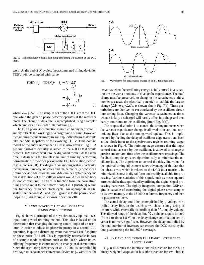
Fig. 6. Synchronously-optimal sampling and timing adjustment of the DCOinput.
word. At the end of cycles, the accumulated timing deviationTDEV will be sampled with value
TDEV TDEV
(5)
where . The samples out of the nDCO are at the DCOrate while the generic phase detector operates at the referenceclock. The change of data rate is accomplished using a samplerwhich employs a first-order interpolation [7].
The DCO phase accumulation is not tied to any hardware. Itsimply reflects the workings of a progression of time. However,thesamplingmechanismrequiresanexplicithardwarethatwouldtake periodic snapshots of the evolving TDEV. Time-domainmodel of the entire normalized DCO is also given in Fig. 5. Ageneric hardware circuitry is added to the nDCO that woulddetect TDEV and convert it to the digital bit format. At the sametime, it deals with the troublesome unit of time by performingnormalization to the clock period of the DCO oscillation, definedasunit interval(UI). The diagram does not suggest any particularmechanism, it merely indicates and mathematically describes atimingdeviationdetector thatwoulddetermineanyfrequencyandphase deviations of the oscillator which would then be fed backas loop corrections. The transfer function from the normalizedtuning word input to the detector output is 1 [bits/bits] withinone frequency reference clock cycle. An appropriate digitalscaler/filter between and will give rise to the phase-lockedloop (PLL). An example is shown in Section VIII.
V. SYNCHRONOUSLY OPTIMAL OSCILLATOR
TUNING WORD RETIMING
Fig. 6 shows a principle of the synchronously-optimal DCOinput tuning word retiming method. This idea is based on theobservation that changing the tuning control input of an oscil-lator, in order to adjust its phase/frequency in a normal PLLoperation, is quite a disturbing event that reveals itself as jitteror phase noise [8]–[10]. This is especially noticeable in caseof a sample-mode oscillator, such as the DCO, where its os-cillating frequency is commanded to change at discrete times.Since the oscillating frequency of anLC tank is controlled bya voltage-to-capacitance conversion device (e.g., varactor), the
Fig. 7. Waveforms for capacitance change of anLC-tank oscillator.
instances when the oscillating energy is fully stored in a capac-itor are the worst moments to change the capacitance. The totalcharge must be preserved, so changing the capacitance at thosemoments causes the electrical potential to exhibit the largestchange , as shown plot in Fig. 7(a). These per-turbations are thenAM-to-PM translated by the oscillator circuitinto timing jitter. Changing the varactor capacitance at timeswhen it is fully discharged will hardly affect its voltage and thushardly contribute to the oscillating jitter [Fig. 7(b)].
The proposed solution is to control the timing moments whenthe varactor capacitance change is allowed to occur, thus min-imizing jitter due to the tuning word update. This is imple-mented by feeding the delayed oscillator edge transitions backas the clock input to thesynchronousregister retiming stage,as shown in Fig. 6. The retiming stage ensures that the inputcontrol data, as seen by the oscillator, is allowed to change atprecise andoptimaltime after the oscillator zero crossings. Thefeedback loop delay is set algorithmically to minimize the os-cillator jitter. The algorithm to control the delay line value forthe optimal timing adjustment takes advantage of the fact thatthe phase error, which is related to the DCO jitter metric to beminimized, is now in digital form and readily available for pro-cessing. Various statistics of this signal, such as mean squarederror, could be thus optimized by utilizing the digital signal pro-cessing hardware. The tightly-integrated companion DSP en-gine is capable of transferring the digital phase error samplesto its own memory at the 13-MHz reference frequency and thento postprocess them.
The actual delay could be accomplished by a voltage-con-trolled delay line. In the testchip, we chose a long string ofinverters while externally controlling their supply voltage.The allowed range of the delay line voltage is quite limited(from 1 to about 1.8 V) so the delay change contribution per in-verter is not very significant. However, the delay multiplied bythe total number of inverters can exceed the DCO clock cycle,thus guaranteeing the full 360coverage.
VI. PVT AND ACQUISITION DCO BANKS INTERFACE TO
DIGITAL LOGIC
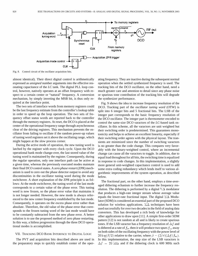
Fig. 8 illustrates the interface control structure for the 8-bitbinary-weighted acquisition bits (the structure for PVT bits is
820 IEEE TRANSACTIONS ON CIRCUITS AND SYSTEMS—II: ANALOG AND DIGITAL SIGNAL PROCESSING, VOL. 50, NO. 11, NOVEMBER 2003
Fig. 8. Control circuit of the oscillator acquisition bits.
almost identical). Their direct digital control is arithmeticallyexpressed asunsignednumber arguments into the effective res-onating capacitance of theLC tank. The digital PLL loop con-trol, however, natively operates at an offset frequency with re-spect to a certain center or “natural” frequency. A conversionmechanism, by simply inverting the MSB bit, is thus only re-quired at the interface point.
The two sets of interface words from memory registers couldbe the last frequency estimate from the controller’s lookup tablein order to speed up the loop operation. The two sets of fre-quency offset status words are reported back to the controllerthrough the memory registers. At reset, the DCO is placed at thecenter of the operational frequency range through asynchronousclear of the driving registers. This mechanism prevents the os-cillator from failing to oscillate if the random power-up valuesof tuning word registers set it above the oscillating range, whichmight happen at the slow process corner.
During the active mode of operation, the new tuning word islatched by the register with every clock cycle. Upon the DCOoperational bank mode change-over, the last stored value of thetuning word is maintained by the register. Consequently, duringthe regular operation, only one interface path can be active ata given time, whereas the previously executed modes maintaintheir final DCO control states. Azero phase restart(ZPR) mech-anism is used to zero out the phase detector output to avoid anydiscontinuities in the oscillator tuning word during the modeswitchover. A short explanation of the ZPR principle is as fol-lows: At the mode switchover, the tuning word of the last modecorresponds to a certain value of the phase error. This tuningword is now frozen, so the phase error value that maintains itis not longer needed. However, the new mode is always refer-enced to the new center frequency established by the last mode.Consequently, it operates on theexcessphase error rather thanabsolute. Therefore, the old value of the phase error that corre-sponds to the frozen tuning word of the last mode would haveto be constantly subtracted from the new phase error. A bettersolution is to use the proposed method of zero phase restarting.In this way, a hitless progression through the three DCO opera-tional modes is accomplished.
VII. T RACKING DCO BANK INTERFACE TODIGITAL LOGIC
The PVT and acquisition bits described above are used inthe preparatory steps to quickly establish center of the oper-
ating frequency. They are inactive during the subsequent normaloperation when the settled synthesized frequency is used. Thetracking bits of the DCO oscillator, on the other hand, need amuch greater care and attention to detail since any phase noiseor spurious tone contribution of the tracking bits will degradethe synthesizer performance.
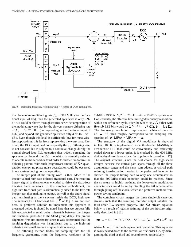
Fig. 9 shows the idea to increase frequency resolution of theDCO. Tracking part of theoscillator tuning word(OTW) issplit into 6 integer bits and 5 fractional bits. The LSB of theinteger part corresponds to the basic frequency resolution ofthe DCO oscillator. The integer part is thermometer encoded tocontrol the same-size DCO varactors of theLC-based tank os-cillator. In this scheme, all the varactors are unit weighted buttheir switching order is predetermined. This guarantees mono-tonicity and helps to achieve an excellent linearity, especially iftheir switching order agrees with the physical layout. The tran-sients are minimized since the number of switching varactorsis no greater than the code change. This compares very favor-ably with the binary-weighted control, where an incrementalchange can cause all the varactors to toggle. In addition, due toequal load throughout for all bits, the switching time is equalizedin response to code changes. In this implementation, a slightlymore general unit-weighted capacitance control is used to addsome extra coding redundancy which lends itself to various al-gorithmic improvements of the system operation, as describedbelow.
The fractional part, on the other hand, employs a time-aver-aged dithering echanism to further increase the frequency res-olution. The dithering is performed by a digital modulatorthat produces a high-rate integer stream whose average valueequals the lower-rate fractional input. The digital Modu-lator (SDM) is considered an essential part of the proposed DCOsolution for wireless applications. techniques have beenused successfully for over two decades in the field of analog dataconverters. This has developed a rich body of knowledge forother applications to draw upon [11]. A simple first-order SDMpattern [12] is not random at all and is likely to create spurioustones. If the LSB varactor has a frequency resolution ofandis dithered at a rate of then it will produce two spurs awayon both sides of the oscillating frequency with the power level of
relative to the carrier, where .In this implementation, the step size of the LSB varactors is
and if the dithering clock is 600 MHz such
STASZEWSKIet al.: DIGITALLY CONTROLLED OSCILLATOR (DCO)-BASED ARCHITECTURE 821
Fig. 9. Improving frequency resolution with�� dither of DCO tracking bits.
that the maximum dithering rate (for the frac-tional input of 0.5), then the generated spur level is only92dBc. It could be shown through Fourier series decomposition ofthe modulating wave that for the slowest nonzero dithering rateof (corresponding to the fractional input of1/32) and beyond, the generated spur rises only 4 dB to88.3dBc. Even though this level is sufficiently low for most wire-less applications, it is far from representing the worst case. Firstof all, the DCO input, and consequently the dithering rate,is not constant but is subject to a continual change during thenormal closed-loop PLL operation thus widely spreading thespur energy. Second, the modulator is normally selectedto operate in the second or third order to further randomize thedithering pattern. With such insignificant amount of quan-tization energy, no phase noise degradation could be observedin our system during normal operation.
The integer part of the tuning word is then added to theinteger-valued high-rate-dithered fractional part. The resultingbinary signal is thermometer encoded to drive the sixty-fourtracking bank varactors. In this simplest embodiment, thehigh-rate fractional part is arithmetically added to the low-rateinteger part thus making its output, as well as the entire signalpath terminating at the varactors inside the DCO, high rate.The separate DCO fractional bits of Fig. 1 are not usedhere. A preferred solution to implement this approach ispresented below. It should be noted here that we purposefullyleft uncorrected a small delay mismatch between the integerand fractional parts due to the SDM group delay. The precisealignment was not necessary since it was determined that theresulting degradation was insignificant due to the high-ratedithering and small amount of quantization energy.
The dithering method trades the sampling rate for thefrequency granularity. Here, the frequency resolution of the
2.4-GHz DCO is with a 13-MHz update rate.Consequently, the effective time-averaged frequency resolution,within one reference cycle, after the 600 MHz dither withfive sub-LSB bits would be .The frequency resolution improvement achieved here is
. This roughly corresponds to the sampling ratespeedup of .
The structure of the digital modulator is depictedin Fig. 10. It is implemented as a third-order MASH-typearchitecture [13] that could be conveniently and efficientlyscaled down to a lower order. It is clocked by the 600 MHzdivided-by-4 oscillator clock. Its topology is based on [12].The original structure is not the best choice for high-speeddesigns because the critical path spans through all the threeaccumulator stages and the carry sum adders. A critical pathretiming transformation needed to be performed in order toshorten the longest timing path to only one accumulator sothat the 600-MHz clock operation could be reached. Sincethe structure is highly modular, the lower-order modulationcharacteristics could be set by disabling the tail accumulatorsthrough gating off the clock, which is a preferred method frompower saving standpoint.
The combiner circuit merges the three single-bit carry-outstreams such that the resulting multi-bit output satisfies thethird-order spectral property. The stream equationbelow is a result of register retiming of the architecture origi-nally described in [12]
(6)
where is the delay element operation. This equationis easily scaled down to the second- or first-order by disre-garding the third or third and second terms, respectively.

822 IEEE TRANSACTIONS ON CIRCUITS AND SYSTEMS—II: ANALOG AND DIGITAL SIGNAL PROCESSING, VOL. 50, NO. 11, NOVEMBER 2003
Fig. 10. MASH-3�� digital modulator structure.
Fig. 11. Implementation block diagram of the DCO tracking bits with DEM of the integer part and�� dithering of the fractional part. Critical high-speedarithmetic operations are performed in “analog” domain through capacitative additions inside the DCO.
Fig. 11 reveals the preferred method of implementing theinteger and fractional oscillator tracking control from a lowerpower standpoint. The fractional path of the DCO tracking bits,which undergoes high-rate dithering, is entirely separated fromthe lower-rate integer part. It even has a dedicated DCO inputjust to avoid “contaminating” the rest of the tracking bits withfrequent transitions. The switch matrix, together with the rowand column select logic, operates as a binary-to-unit-weight en-coder in response to the integer part of the tracking tuning word.The modulator is responsive to only the fractional part ofthe tracking tuning word. The actual merging of both parts isperformed inside the oscillator through time-averaged capaci-tance summation at theLC tank.
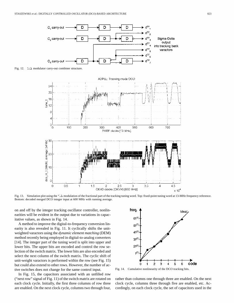
Another important benefit of the chosen approach is thatthe high-speed arithmetic operation of the (6) combiner is nowtrivial. Fig. 12 shows the proposed implementation. All that isrequiredare flip-flop registers(for thedelayoperation)withcom-plementary outputs (for the negation). The arithmetic addition isperformed inside the oscillator through capacitance summation.
Fig. 13 illustrates the second-order MASH-type mod-ulation of the fixed-point tracking DCO tuning control wordwith five-fractional bits. The fixed-point tuning word (upperplot) consists of six-integer bits and five fractional bits and isclocked at the 13-MHz reference frequency. The modulatesthe five-bit fractional part at 600-MHz clock rate and outputs theinteger stream that controls the DCO frequency. The lower plotshows the output stream “merged” with the 6-bit integerpart stream. For the purposes of visualization only, the integerstream is mathematically decoded into an unsigned number rep-resentation and added to the mathematically decoded signedfractional stream.
A. Dynamic Element Matching of the Varactors
Ideally, each of the unit-weighted capacitors of the trackingbank has the exact same capacitative value. Using real-worldfabrication process, however, the capacitative value of each ca-pacitor will vary slightly from the ideal. As capacitors are turned
STASZEWSKIet al.: DIGITALLY CONTROLLED OSCILLATOR (DCO)-BASED ARCHITECTURE 823
Fig. 12. �� modulator carry-out combiner structure.
Fig. 13. Simulation plot using the��modulation of the fractional part of the tracking tuning word. Top: fixed-point tuning word at 13-MHz frequency reference.Bottom: decoded merged DCO integer input at 600 MHz with running average.
on and off by the integer tracking oscillator controller, nonlin-earities will be evident in the output due to variations in capac-itative values, as shown in Fig. 14.
A method to improve the digital-to-frequency conversion lin-earity is also revealed in Fig. 11. It cyclically shifts the unit-weighted varactors using thedynamic element matching(DEM)method recently being employed in digital-to-analog converters[14]. The integer part of the tuning word is split into upper andlower bits. The upper bits are encoded and control the row se-lection of the switch matrix. The lower bits are also encoded andselect the next column of the switch matrix. The cyclic shift ofunit-weight varactors is performed within the row (see Fig. 15)but could also extend to other rows. However, the number of ac-tive switches does not change for the same control input.
In Fig. 15, the capacitors associated with an unfilled row(“next row” signal of Fig. 11) of the switch matrix are rotated oneach clock cycle. Initially, the first three columns of row threeare enabled. On the next clock cycle, columns two through four,
Fig. 14. Cumulative nonlinearity of the DCO tracking bits.
rather than columns one through three are enabled. On the nextclock cycle, columns three through five are enabled, etc. Ac-cordingly, on each clock cycle, the set of capacitors used in the

824 IEEE TRANSACTIONS ON CIRCUITS AND SYSTEMS—II: ANALOG AND DIGITAL SIGNAL PROCESSING, VOL. 50, NO. 11, NOVEMBER 2003
Fig. 15. Dynamic element matching through cyclic shift within a matrix row.
64-element array changes slightly. Over time, the nonlinearitiesshown in Fig. 14 average out, thereby producing a much moreaccurate output.
With this DEM scheme, the enabled switches for a singlerow are rotated. This is accomplished by modulo incrementingthe starting column of the enabled switches on each clockcycle. This method could be varied slightly by including two(or more) rows in the rotation. As a result, a larger frequencyrange would be subject to the beneficial time averaging, byincluding a greater number of capacitors in the rotation, but ata cost of a longer repetition cycle. An alternative method ofincreasing the DEM frequency span would be to lengthen thenumber of columns per row, thus creating a nonsquare matrix.
The output bits of the switch matrix are individually cou-pled to the bank of sixty-four resampling drivers, which are im-plemented as flip-flop registers. Each driver controls a singleunit-weighted varactor of theLC tank. Using resampling by theclock eliminates delay mismatches due to path differences, suchthat the timing points of varactor transitions coincide. This helpswith the spurious noise control. It should be noted that whilethe switch matrix is shown (from an algorithmic standpoint) ina row/column configuration, the actual implementation is not aprecise grid. In fact, a group of rows could be physically com-bined into a single line.
The principal difference in DFC versus DAC specificationrequirements is that the full dynamic range is not required forthe available number of controlled units. In the DFC application,the frequency headroom is required because it is not expectedthat the oscillator operates at the precisely specified frequencybefore entering the tracking mode.
B. DCO Varactor Rearrangement
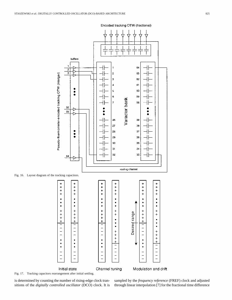
As illustrated in Fig. 16, the sixty-four integer tracking-bitvaractors of theLC tank have a physical layout of two longcolumns and the fractional tracking-bit varactors are arrangedseparately. However, the controlling circuitry is located only onone side. This creates an unbalanced structure in which routingto one varactor column is significantly shorter with easier ac-cess than to the other and, therefore, their transient response isdifferent. Moreover, the spatially separated devices are likely to
be more mismatched due to the process gradient. If, during thecourse of operation, the varactor selection transitions throughthe column boundary, it is likely to create larger switching per-turbations. It is proposed that before entering the finest trackingmode, a rearrangement of DCO varactors to be performed suchthat “lower quality” capacitors be filled in order to maximize thefrequency dynamic range of the most preferred capacitor sec-tion. In this architecture, this could be done upon switchoverfrom fast tracking to tracking.
It should be noted that, while in other designs, the trackingcapacitors could be arranged differently depending upon variouslayout issues, a certain set of capacitors will always be favoredbased on the proximity metric to the control logic.
Fig. 17 illustrates a method of improving the quality of theDFC conversion. In the initial state, half of the capacitors ineach column are turned on (as designated by a “”) and halfare turned off (as designated by a “”). During fast tracking, thecapacitors of the less desirable right-hand column are enabledor disabled in order to fine tune the oscillator to the selectedchannel, to the extent possible. If additional capacitors need tobe enabled or disabled, the capacitors from the left-hand columnmay be used, preferably those capacitors at the edges of thecolumn. After channel tuning, the capacitors in the left-handcolumn are used for modulation and drift control. In this way,the most desirable capacitors are used for maintaining lock andfor generating the signal once data is being transmitted.
VIII. E XAMPLE OF A DIGITAL PLL ARCHITECTURE
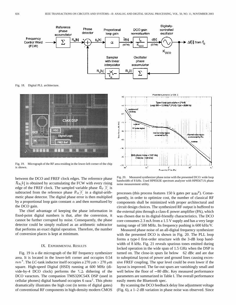
The presented DCO-based system architecture allows forthe frequency synthesizer to be implemented in a fully-digitalmanner and places little restrictions on the specific architectureof the PLL loop. For this reason, the phase detector mechanismdepicted in Fig. 4 was described in generic terms. Since thefocus of this paper is on the DCO and its surrounding circuitry,a brief description of a specific PLL structure used in our workis provided below as a means of further motivation.
The PLL architecture shown in Fig. 18 belongs to a classof PLL frequency synthesizers operating in the phase-domain,which was proposed in [15]. It is a type-I structure that operatesin a digital fixed-point phase domain. The variable phase
STASZEWSKIet al.: DIGITALLY CONTROLLED OSCILLATOR (DCO)-BASED ARCHITECTURE 825
Fig. 16. Layout diagram of the tracking capacitors.
Fig. 17. Tracking capacitors rearrangement after initial settling.
is determined by counting the number of rising-edge clock tran-sitions of thedigitally controlled oscillator(DCO) clock. It is
sampled by thefrequency reference(FREF) clock and adjustedthrough linear interpolation [7] for the fractional time difference
826 IEEE TRANSACTIONS ON CIRCUITS AND SYSTEMS—II: ANALOG AND DIGITAL SIGNAL PROCESSING, VOL. 50, NO. 11, NOVEMBER 2003
Fig. 18. Digital PLL architecture.
Fig. 19. Micrograph of the RF area residing in the lower-left corner of the chipis shown.
between the DCO and FREF clock edges. The reference phaseis obtained by accumulating the FCW with every rising
edge of the FREF clock. The sampled variable phase issubtracted from the reference phase in a digital-arith-metic phase detector. The digital phase error is then multipliedby a proportional loop gain constantand then normalized bythe DCO gain.
The chief advantage of keeping the phase information infixed-point digital numbers is that, after the conversion, itcannot be further corrupted by noise. Consequently, the phasedetector could be simply realized as an arithmetic subtractorthat performs an exact digital operation. Therefore, the numberof conversion places is kept at minimum.
IX. EXPERIMENTAL RESULTS
Fig. 19 is a die micrograph of the RF frequency synthesizerarea. It is located in the lower-left corner and occupies 0.54
. TheLC-tank inductor itself occupies a 270m 270 msquare. High-speed Digital (HSD) running at 600 MHz (di-vide-by-4 DCO clock) performs the dithering of theDCO varactors. The companion TMS320C54X DSP (used incellular phones) digital baseband occupies 6 . This photodramatically illustrates the high cost (in terms of digital gates)of conventional RF components in high-density modern CMOS
Fig. 20. Measured synthesizer phase noise with the presented DCO: wide loopbandwidth of 8 kHz. Used HP8563E spectrum analyzer with HP85671A phasenoise measurement utility.
processes (this process features 150 k gates per). Conse-quently, in order to optimize cost, the number of classical RFcomponents shall be minimized with proper architectural andcircuit design choices. The synthesized RF output is buffered tothe external pins through a class-E power amplifier (PA), whichwas chosen due to its digital-friendly characteristics. The DCOcore consumes 2.3 mA from a 1.5 V supply and has a very largetuning range of 500 MHz. Its frequency pushing is 600 kHz/V.
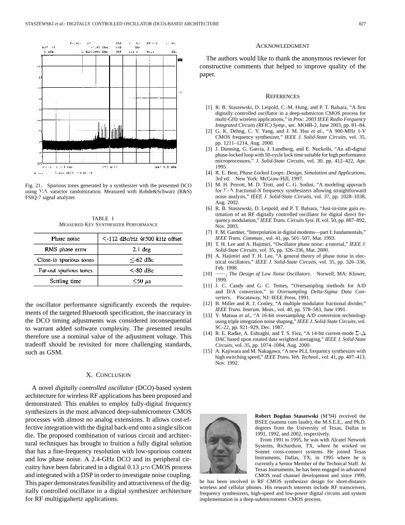
Measured phase noise of an all-digital frequency synthesizerwith the presented DCO is shown in Fig. 20. The PLL loopforms a type-I first-order structure with the 3-dB loop band-width of 8 kHz. Fig. 21 reveals spurious tones emitted duringlocked operation in the wide span of 1.5 GHz when the DSP isturned on. The close-in spurs lie below62 dBc and are dueto suboptimal layout of power and ground lines causing exces-sive FREF coupling. The spur level could be even lower if thelayout is improved. The far-out spurs are vanishingly small andwell below the floor of 80 dBc. Key measured performanceparameters are summarized in Table I. The overall performanceeasily meets the Bluetooth spec.
By scanning the DCO feedback delay line adjustment voltage(Fig. 6), a 1–2 dB variation in phase noise was observed. Since
STASZEWSKIet al.: DIGITALLY CONTROLLED OSCILLATOR (DCO)-BASED ARCHITECTURE 827
Fig. 21. Spurious tones generated by a synthesizer with the presented DCOusing�� varactor randomization. Measured with Rohde&Schwarz (R&S)FSIQ-7 signal analyzer.
TABLE IMEASUREDKEY SYNTHESIZER PERFORMANCE
the oscillator performance significantly exceeds the require-ments of the targeted Bluetooth specification, the inaccuracy inthe DCO timing adjustments was considered inconsequentialto warrant added software complexity. The presented resultstherefore use a nominal value of the adjustment voltage. Thistradeoff should be revisited for more challenging standards,such as GSM.
X. CONCLUSION
A novel digitally controlled oscillator(DCO)-based systemarchitecture for wireless RF applications has been proposed anddemonstrated. This enables to employ fully-digital frequencysynthesizers in the most advanced deep-submicrometer CMOSprocesses with almost no analog extensions. It allows cost-ef-fective integration with the digital back-end onto a single silicondie. The proposed combination of various circuit and architec-tural techniques has brought to fruition a fully digital solutionthat has a fine-frequency resolution with low-spurious contentand low phase noise. A 2.4-GHz DCO and its peripheral cir-cuitry have been fabricated in a digital 0.13 CMOS processand integrated with a DSP in order to investigate noise coupling.This paper demonstrates feasibility and attractiveness of the dig-itally controlled oscillator in a digital synthesizer architecturefor RF multigigahertz applications.
ACKNOWLEDGMENT
The authors would like to thank the anonymous reviewer forconstructive comments that helped to improve quality of thepaper.
REFERENCES
[1] R. B. Staszewski, D. Leipold, C.-M. Hung, and P. T. Balsara, “A firstdigitally controlled oscillator in a deep-submicron CMOS process formulti-GHz wireless applications,” inProc. 2003 IEEE Radio FrequencyIntegrated Circuits (RFIC) Symp., sec. MO4B-2, June 2003, pp. 81–84.
[2] G. K. Dehng, C. Y. Yang, and J. M. Hsuet al., “A 900-MHz 1-VCMOS frequency synthesizer,”IEEE J. Solid-State Circuits, vol. 35,pp. 1211–1214, Aug. 2000.
[3] J. Dunning, G. Garcia, J. Lundberg, and E. Nuckolls, “An all-digitalphase-locked loop with 50-cycle lock time suitable for high performancemicroprocessors,”J. Solid-State Circuits, vol. 30, pp. 412–422, Apr.1995.
[4] R. E. Best,Phase Locked Loops: Design, Simulation and Applications,3rd ed. New York: McGraw-Hill, 1997.
[5] M. H. Perrott, M. D. Trott, and C. G. Sodini, “A modeling approachfor �-� fractional-N frequency synthesizers allowing straightforwardnoise analysis,”IEEE J. Solid-State Circuits, vol. 37, pp. 1028–1038,Aug. 2002.
[6] R. B. Staszewski, D. Leipold, and P. T. Balsara, “Just-in-time gain es-timation of an RF digitally controlled oscillator for digital direct fre-quency modulation,”IEEE Trans. Circuits Syst. II, vol. 50, pp. 887–892,Nov. 2003.
[7] F. M. Gardner, “Interpolation in digital modems—part I: fundamentals,”IEEE Trans. Commun., vol. 41, pp. 501–507, Mar. 1993.
[8] T. H. Lee and A. Hajimiri, “Oscillator phase noise: a tutorial,”IEEE J.Solid-State Circuits, vol. 35, pp. 326–336, Mar. 2000.
[9] A. Hajimiri and T. H. Lee, “A general theory of phase noise in elec-trical oscillators,”IEEE J. Solid-State Circuits, vol. 35, pp. 326–336,Feb. 1998.
[10] , The Design of Low Noise Oscillators. Norwell, MA: Kluwer,1999.
[11] J. C. Candy and G. C. Temes, “Oversampling methods for A/Dand D/A conversion,” in Oversampling Delta-Sigma Data Con-verters. Piscataway, NJ: IEEE Press, 1991.
[12] B. Miller and R. J. Conley, “A multiple modulator fractional divider,”IEEE Trans. Instrum. Meas., vol. 40, pp. 578–583, June 1991.
[13] Y. Matsuaet al., “A 16-bit oversampling A/D conversion technologyusing triple integration noise shaping,”IEEE J. Solid-State Circuits, vol.SC-22, pp. 921–929, Dec. 1987.
[14] R. E. Radke, A. Eshraghi, and T. S. Fiez, “A 14-bit current-mode�-�DAC based upon rotated data weighted averaging,”IEEE J. Solid-StateCircuits, vol. 35, pp. 1074–1084, Aug. 2000.
[15] A. Kajiwara and M. Nakagawa, “A new PLL frequency synthesizer withhigh switching speed,”IEEE Trans. Veh. Technol., vol. 41, pp. 407–413,Nov. 1992.
Robert Bogdan Staszewski(M’94) received theBSEE (summa cum laude), the M.S.E.E., and Ph.D.degrees from the University of Texas, Dallas in1991, 1992, and 2002, respectively.
From 1991 to 1995, he was with Alcatel NetworkSystems, Richardson, TX, where he worked onSonnet cross-connect systems. He joined TexasInstruments, Dallas, TX, in 1995 where he iscurrently a Senior Member of the Technical Staff. AtTexas Instruments, he has been engaged in advancedCMOS read channel development and since 1999,
he has been involved in RF CMOS synthesizer design for short-distancewireless and cellular phones. His research interests include RF transceivers,frequency synthesizers, high-speed and low-power digital circuits and systemimplementation in a deep-submicrometer CMOS process.
828 IEEE TRANSACTIONS ON CIRCUITS AND SYSTEMS—II: ANALOG AND DIGITAL SIGNAL PROCESSING, VOL. 50, NO. 11, NOVEMBER 2003
Dirk Leipold received the Diploma and Ph.D.degrees in physics from the University of Konstanz,Germany, in 1991 and 1995, respectively.
From 1991 to 1995, he was with the Paul ScherrerInstitute, Zurich, Switzerland, where he workedon Smart pixel optoelectronics. In 1995, he joinedTexas Instruments, Germany, where he was involvedin RF process integration, device characterization,and modeling, and in the development of RF-CMOStechnologies on high-resistivity substrates. From1998 to 1999, he represented Texas Instruments
in the ETSI Hiperlan2 Committee, where he was Editor for the PHY layertechnical specification. In 1999, he moved to Texas Instruments, Dallas, wherehe is currently Manager of the Digital Radio Processor Architecture Group. Hisresearch interests include advanced RF architectures, nanometer scale CMOSprocess, and quantum electronics.
Khurram Muhammad received the B.Sc. degreefrom the University of Engineering and Technology,Lahore, Pakistan, in 1990, the M. Eng. SC. degreefrom the University of Melbourne, Parkville,Victoria, Australia, in 1993, and the Ph.D. degreefrom Purdue University, West Lafayette, IN in 1999.
From 1990 to 1991 and 1993 to 1994, he workedwith Carrier Telephone Industries, Islamabad,Pakistan, in Research and Development where hewas involved in the development of board leveldesigns for rural and urban telecommunication
projects. From 1994 to 1995, he was a Research Associate, Department ofElectronic Engineering, Ghulam Ishaq Khan Institute of Engineering Scienceand Technology. In 1995, he was with Hong Kong University of Science andTechnology, Kowloon, where he developed fast simulation techniques forDS/CDMA systems in multipath fading. Since 1999, he has been working atTexas Instruments Inc., Dallas.
Poras T. Balsara(S’83–M’85–SM’95) received theL.E.E. diploma in electronics from The Victoria Ju-bilee Technical Institute, Bombay, India in 1980, theB.E. degree from the University of Bombay, India, in1983, and the M.S. and Ph.D. degrees in computerscience from Pennsylvania State University, Univer-sity Park, in 1985 and 1989, respectively.
Currently, he is a Professor of Electrical Engi-neering with the Erik Jonsson School of Engineeringand Computer Science, The University of Texas atDallas, Richardson. His research interests include,
VLSI design, design of energy efficient digital circuits and systems, computerarithmetic, application-specific architecture design, and reconfigurable com-puting. He has published several journal and conference papers in these areas.