direct creation of microdomains with positive and negative ... · 2materials and surface science...
TRANSCRIPT

Direct creation of microdomains with positive and negative surfacepotential on hydroxyapatite coatingsT. Plecenik, S. A. M. Tofail, M. Gregor, M. Zahoran, M. Truchly et al. Citation: Appl. Phys. Lett. 98, 113701 (2011); doi: 10.1063/1.3567532 View online: http://dx.doi.org/10.1063/1.3567532 View Table of Contents: http://apl.aip.org/resource/1/APPLAB/v98/i11 Published by the American Institute of Physics. Related ArticlesRemarkable current-enhanced photoconductivity in oxygen-deficient La7/8Sr1/8MnO3−δ thin film Appl. Phys. Lett. 101, 042413 (2012) Epitaxial strain-induced changes in the cation distribution and resistivity of Fe-doped CoFe2O4 Appl. Phys. Lett. 101, 021907 (2012) Magnetotransport anisotropy in lattice-misfit-strained ultrathin La2/3Ca1/3MnO3 films epitaxially grown on (110)-oriented SrTiO3 and LaAlO3 substrates J. Appl. Phys. 112, 013907 (2012) Anisotropic electrical properties in bismuth layer structured dielectrics with natural super lattice structure Appl. Phys. Lett. 101, 012907 (2012) Resistive switching behavior of a thin amorphous rare-earth scandate: Effects of oxygen content Appl. Phys. Lett. 101, 012102 (2012) Additional information on Appl. Phys. Lett.Journal Homepage: http://apl.aip.org/ Journal Information: http://apl.aip.org/about/about_the_journal Top downloads: http://apl.aip.org/features/most_downloaded Information for Authors: http://apl.aip.org/authors
Downloaded 26 Jul 2012 to 130.209.6.40. Redistribution subject to AIP license or copyright; see http://apl.aip.org/about/rights_and_permissions

Direct creation of microdomains with positive and negative surfacepotential on hydroxyapatite coatings
T. Plecenik,1,a� S. A. M. Tofail,2 M. Gregor,1 M. Zahoran,1 M. Truchly,1 F. Laffir,2 T. Roch,1
P. Durina,1 M. Vargova,3 G. Plesch,3 P. Kus,1 and A. Plecenik1
1Department of Experimental Physics, Faculty of Mathematics, Physics and Informatics,Comenius University, 842 48 Bratislava, Slovakia2Materials and Surface Science Institute, University of Limerick, Limerick, Ireland3Department of Inorganic Chemistry, Faculty of Natural Sciences, Comenius University,842 15 Bratislava, Slovakia
�Received 5 November 2010; accepted 24 February 2011; published online 16 March 2011�
A method for the direct patterning of electrostatic potential at the surface of hydroxyapatite ispresented here. Microdomains of surface potential have been created on hydroxyapatite coatings bya 20 keV focused electron beam with minimal alterations of surface chemistry. The success of suchapproach has been confirmed by Kelvin probe force microscopy measurements, which show thatthis method is capable of creating micron sized positive and negative local electrostatic potential.The shape and potential difference of these domains were found to depend on the dose of totalinjected charge from the electron beam as well as the speed with which such charge is injected.© 2011 American Institute of Physics. �doi:10.1063/1.3567532�
Modifications of biomaterials surfaces in terms of theirwettability and surface potential �SP� play an important rolein biological and medical applications as these are consid-ered to be key factors that influence the adhesion and thegrowth of proteins, cells, and bacteria on implant surfaces.1,2
Various methods have been used to modify surface proper-ties of biomaterials in order to control its interactions withproteins and biological cells. These include inter alia theapplication of an external electric field2 �e.g., contact poling�,ion or electron beam,3–7 photon irradiation,8 low and highpressure plasma,8 and chemical, and electrochemical modifi-cations. Of particular interest is the method proposed byAronov et al.,4–7 where such surface modifications have beenobtained through a low-energy �100 eV� electron irradiationmethod. These authors have demonstrated an ability to adjustSP and wettability �and thus also protein and bacterial adhe-sion� of hydroxyapatite �HA� in a wide range of contactangles. These authors irradiated either the whole sample sur-face or large areas �500 �m diameter� of HA ceramic pelletsthrough a prepatterned Si-mask and reported the creation of anegative SP only.
Here, we report a convenient technique of direct micro-scopic patterning of SP, i.e., without the need of any mask. Inthis technique, microdomains of modified SP have been cre-ated on HA �Ca10�PO4�6�OH�2� coatings by focused 20 keVelectron beam, typically available as an electron microprobein a scanning electron microscope �SEM�. In contrast withthe earlier investigations,4–7 our work shows that by varyingthe dosage and speed of electron injection it is possible tocreate circular, doughnut shaped, and bimodal micrometer-sized patterns with positive and negative SP.
HA thin films have been deposited on Si substrates byspin-coating through a sol-gel synthesis route. For the sol-gelpreparation, phosphoric pentaoxide �P2 O5� and calcium ni-trate tetrahydrate �Ca�NO3�2 ·4H2 O� have been dissolved inpure ethanol to prepare a 0.5 mol/l and a 1.67 mol/l solu-
tions, respectively. The precursor sol is then obtained bymixing the two solutions in a proportion to obtain a Ca/Pmolar ratio of 1.67. The mixture is continuously stirred atroom temperature and subsequently heated to 70 °C for 1 h,resulting in a transparent sol-gel, which is spin coated on ap-type �100� Si at 4000 rpm for 50 s. The deposited film onSi is then aged at 100 °C temperature for 30 min and cal-cined in air at 700 °C for 1 h. The phase purity and thesurface concentration of the calcined film have been verifiedby x-ray diffraction �XRD: Philips X’Pert Pro� and x-rayphotoelectron spectroscopy �XPS: Kratos Axis 165�.
The thickness of the films has been determined in cross-section with a SEM TESCAN TS 5136 MM to be about 650nm. The film surface morphology has also been inspectedwith SEM. For the electron beam modification, a matrix of2�2 points has been irradiated by focused electron beamwith an absorbed beam current ranging from 1.4 to 14 nAand a beam diameter ranging from 120 nm for the lowestcurrent �1.4 nA� to 750 nm for the highest current �14 nA�used. The beam exposure time has also been varied from 1 to700 s/exposure point. In all cases, the electron energy is keptconstant at 20 keV at a vacuum of 10−4 Pa.
A scanning probe microscope �NT-MDT Solver P47PRO� in a semicontact atomic force microscopy �AFM� andKelvin probe force microscopy �KPFM� modes has beenused for the measurements of the surface topography and SPof the HA films, respectively. TiN-coated silicon AFMprobes have been used for KPFM measurements, which si-multaneously provided topographic images. The AFM sur-face topography images showed the nanocrystalline nature ofthe calcined film although some nanoscale porosity was alsovisible. This nanocrystalline morphology has further beenconfirmed by SEM and XRD.
Table I compares the surface chemistry of the untreatedand irradiated HA films. In the latter case, an array of 80�80 microdomains was directly created over an area of1 mm2. Each of these microdomains was created by expos-ing to a 20 keV focused electron beam with a 14 nA beama�Electronic mail: [email protected].
APPLIED PHYSICS LETTERS 98, 113701 �2011�
0003-6951/2011/98�11�/113701/3/$30.00 © 2011 American Institute of Physics98, 113701-1
Downloaded 26 Jul 2012 to 130.209.6.40. Redistribution subject to AIP license or copyright; see http://apl.aip.org/about/rights_and_permissions
current. The exposure time was varied for 1 and 7 s. Thechange in surface chemistry due to the electron irradiation isnegligible and is mainly confined within the adsorbed overlayer.
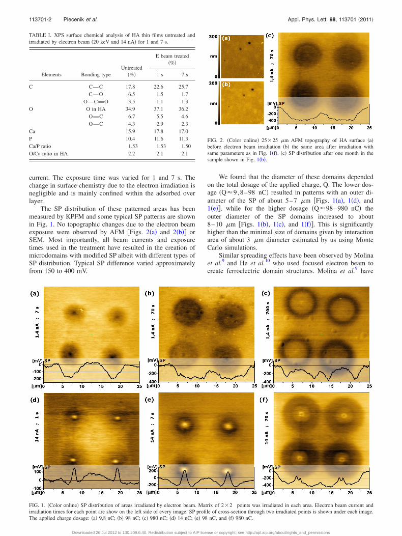
The SP distribution of these patterned areas has beenmeasured by KPFM and some typical SP patterns are shownin Fig. 1. No topographic changes due to the electron beamexposure were observed by AFM �Figs. 2�a� and 2�b�� orSEM. Most importantly, all beam currents and exposuretimes used in the treatment have resulted in the creation ofmicrodomains with modified SP albeit with different types ofSP distribution. Typical SP difference varied approximatelyfrom 150 to 400 mV.
We found that the diameter of these domains dependedon the total dosage of the applied charge, Q. The lower dos-age �Q�9,8–98 nC� resulted in patterns with an outer di-ameter of the SP of about 5–7 �m �Figs. 1�a�, 1�d�, and1�e��, while for the higher dosage �Q�98–980 nC� theouter diameter of the SP domains increased to about8–10 �m �Figs. 1�b�, 1�c�, and 1�f��. This is significantlyhigher than the minimal size of domains given by interactionarea of about 3 �m diameter estimated by us using MonteCarlo simulations.
Similar spreading effects have been observed by Molinaet al.9 and He et al.10 who used focused electron beam tocreate ferroelectric domain structures. Molina et al.9 have
TABLE I. XPS surface chemical analysis of HA thin films untreated andirradiated by electron beam �20 keV and 14 nA� for 1 and 7 s.
Elements Bonding typeUntreated
�%�
E beam treated�%�
1 s 7 s
C CuC 17.8 22.6 25.7CuO 6.5 1.5 1.7
OuCvO 3.5 1.1 1.3O O in HA 34.9 37.1 36.2
OvC 6.7 5.5 4.6OuC 4.3 2.9 2.3
Ca 15.9 17.8 17.0P 10.4 11.6 11.3Ca/P ratio 1.53 1.53 1.50O/Ca ratio in HA 2.2 2.1 2.1
FIG. 1. �Color online� SP distribution of areas irradiated by electron beam. Matrix of 2�2 points was irradiated in each area. Electron beam current andirradiation times for each point are show on the left side of every image. SP profile of cross-section through two irradiated points is shown under each image.The applied charge dosage: �a� 9,8 nC; �b� 98 nC; �c� 980 nC; �d� 14 nC; �e� 98 nC, and �f� 980 nC.
FIG. 2. �Color online� 25�25 �m AFM topography of HA surface �a�before electron beam irradiation �b� the same area after irradiation withsame parameters as in Fig. 1�f�. �c� SP distribution after one month in thesample shown in Fig. 1�b�.
113701-2 Plecenik et al. Appl. Phys. Lett. 98, 113701 �2011�
Downloaded 26 Jul 2012 to 130.209.6.40. Redistribution subject to AIP license or copyright; see http://apl.aip.org/about/rights_and_permissions

attributed such effect to a migration of charge carriers insidethe material caused by local electric fields induced by theirradiation. On the other hand, the electron beam can be sig-nificantly defocused when the sample surface is charged.This could be an additional factor responsible for broadeningof the domains at higher exposure times. There is also apossibility of the progressive spread of thermal damage al-though XPS results in Table I rules out any such effects.
Interestingly, the speed of charge injection, measured asthe absorbed beam current greatly influences the resultingshape and distribution of the SP. The lower absorbed currents�1.4 nA� and thus slower charge injection are capable ofcreating domains only with negative SP �Figs. 1�a�–1�c��with respect to the unexposed surroundings, the SP of whichis referenced as a zero potential. A similar amount of charge,when injected faster �14 nA absorbed beam current�, createsdomains with a bimodal distribution of positive �Figs. 1�d�and 1�e�� or less-negative �Fig. 1�f�� SP surrounded by anegative annulus of SP. Aronov et al.6 have also observednegative SP in HA but in areas exposed to low-energy �100eV� electron irradiation. They propose that the impactingelectrons generate electron-hole pairs, which are subse-quently localized �together with primary electrons� by trapsof different origin. As electrons have higher mobility, theymay occupy bulk traps, or in our case, further surface traps.Holes can be trapped only by surface traps within close vi-cinity of the irradiation region, which in our case is hundredsof nanometers in diameter. This may lead to the bimodal SPdistribution observed in Figs. 1�d� and 1�e�. Moreover, theemission of secondary electrons may leave positivelycharged holes at the surface11 and give rise to positive SPs asobserved in Figs. 1�d� and 1�e� when HA was irradiated withelectron beam with relatively higher charge injection. Theintensity of these positively charged areas increased initially�Fig. 1�e��. If the domains were exposed for sufficiently longtime, incoming electrons could neutralize these positivelycharged areas although leaving them still less negativelycharged than the areas where no such positive charge wascreated �Fig. 1�f��. Furthermore, local electric field-inducedpolarization,12 and creation of carbon/hydrocarbon surfacecontamination layer in SEM �Ref. 4� may influence the re-sulting SP distribution. While more fundamental study willbe necessary to distinguish the influence of a particular pro-cess in creating these domains, the creation of positivelycharged areas will be interesting to study specific binding ofnegatively charged proteins and cell membranes.
These domains are stable in air when kept at room tem-perature. After one month, there was no significant differencein the size, shape or SP when compared to the measurementsdone immediately after the treatment �Fig. 2�c��. Thus, weexpect that such domains can be stable for several monthswhen stored in air and will facilitate practical applications.Such long-term stability is in agreement with the observa-
tions by Aronov et al.,4–7 where wettability and SP modifi-cations of HA obtained by low-energy electron irradiationwere stable for at least one month without any chemical orstructural damage. Our study confirms these findings and ex-tends to interactions with higher energy electron beam �20keV�. It is known that structural alterations of HA can occurif exposed to 100–400 keV electron beam energy, e.g., asreported by Huaxia and Marquis13 during transmission elec-tron microscopy. XPS data presented in Table I establishesthat such damage is unlikely to take place for the beam en-ergy used in this study.
To conclude, microdomains �5–10 �m diameter� withmodified SPs were patterned on HA coatings by a focused 20keV electron beam from a SEM microscope. We have shownthat this method can conveniently create microdomains withboth positively and negatively modified SPs with respect tothe untreated area. The size of these domains depends mostlyon total electric charge injected, while the polarity and theshape depend on the speed of the charge injection �i.e., beamcurrent�. We have also shown that when stored in air, thesedomains are stable for at least one month.
This project has been funded with support from the Eu-ropean Commission �Grant No. EC NMP4-SL-2008-212533—BioElectricSurface�. This publication reflects theviews only of the authors, and the Commission cannot beheld responsible for any use which may be made of the in-formation contained therein. This work was also supportedby the Slovak Research and Development Agency under theContract No. DO7RP-007-09 and is also the result of theproject implementation: Grant No. 26240120012 supportedby the Research & Development Operational Programmefunded by the ERDF.
1Y. H. An and R. J. Friedman, J. Biomed. Mater. Res. 43, 338 �1998�.2R. Kato, S. Nakamura, K. Katayama, and K. Yamashita, J. Biomed. Mater.Res. A 74A, 652 �2005�.
3F. Z. Cui and Z. S. Luo, Surf. Coat. Technol. 112, 278 �1999�.4D. Aronov, R. Rosen, E. Z. Ron, and G. Rosenman, Surf. Coat. Technol.
202, 2093 �2008�.5D. Aronov, R. Rosen, E. Z. Ron, and G. Rosenman, Process Biochem.�Oxford, U.K.� 41, 2367 �2006�.
6D. Aronov, G. Rosenman, A. Karlov, and A. Shashkin, Appl. Phys. Lett.88, 163902 �2006�.
7D. Aronov, A. Karlov, and G. Rosenman, J. Eur. Ceram. Soc. 27, 4181�2007�.
8I. Pashkuleva, A. P. Marques, F. Vaz, and R. L. Reis, J. Mater. Sci. Mater.Med. 21, 21 �2010�.
9P. Molina, M. O. Ramírez, J. García-Sole, and L. E. Bausá, Opt. Mater.�Amsterdam, Neth.� 31, 1777 �2009�.
10J. He, S. H. Tang, Y. Q. Qin, P. Dong, H. Z. Zhang, C. H. Kang, W. X.Sun, and Z. X. Shen, J. Appl. Phys. 93, 9943 �2003�.
11R. Gerhard-Multhaupt, IEEE Trans. Electr. Insul. EI-22, 531 �1987�.12R. Danz, M. Pinnow, A. Büchtemann, and A. Wedel, IEEE Trans. Electr.
Insul. 5, 16 �1998�.13J. Huaxia and P. M. Marquis, J. Mater. Sci. Lett. 10, 132 �1991�.
113701-3 Plecenik et al. Appl. Phys. Lett. 98, 113701 �2011�
Downloaded 26 Jul 2012 to 130.209.6.40. Redistribution subject to AIP license or copyright; see http://apl.aip.org/about/rights_and_permissions