direct digital synthesizer (dds) - university of maine · direct digital synthesizer (dds) ... 12...
TRANSCRIPT

Direct Digital Synthesizer (DDS)
Ognjen NikolicECE547 VLSI Design/Layout
University of MaineOrono, Maine 04473
United States
May 12, 2005

Direct Digital Synthesizer (DDS)
Ognjen NikolicECE547 VLSI Design/Layout
University of MaineOrono, Maine 04473
United States
May 12, 2005

Abstract
The Direct Digital Synthesizer IC was designed to meet the requirements specified by the graduate
level course in electrical engineering (ECE 547 VLSI Design/Layout) at the University of Maine at
Orono. The Direct Digital Synthesizer (DDS) produces a sine wave by generating a time-varying signal
in digital form and then performing a digital-to-analog conversion. The desired frequency of the output
sine wave is specified by 12 digital inputs. The DDS consists of three major building blocks including
12 Bit Accumulator, 256 Byte ROM and 10 Bit Analog to Digital Converter. Utilizing the software
approach vs. a hardware approach to modify the frequency of a periodic waveform provides increased
development flexibility and decreased verification time. Because operations within the DDS are
primarily digital, the chip can offer fast switching between output frequencies, fine frequency
resolution, and operation over a broad spectrum of frequencies.
i

TABLE OF CONTENTS
Abstract ................................................................................................................................................ iTABLE OF CONTENT........................................................................................................................ iiiTABLE OF FIGURES.......................................................................................................................... iii
1 INTRODUCTION..............................................................................................................................1 1.1 Background................................................................................................................................ 1
2 PRODUCT DESCRIPTION.............................................................................................................. 2 2.1 Theory of DDS Operation.......................................................................................................... 2 2.2 Block Diagram Description........................................................................................................3 2.2.1 Phase Accumulator ............................................................................................................4 2.2.2 Sine Look-Up Table (ROM) ............................................................................................. 5 2.2.3 Digital to Analog Converter .............................................................................................. 5 2.2.4 Interfacing ......................................................................................................................... 6 2.3 Summary.................................................................................................................................... 7
3 SCHEMATICS...................................................................................................................................8 3.1 Accumulator............................................................................................................................... 8 3.2 ROM Pointer.............................................................................................................................. 11
4 LAYOUT........................................................................................................................................... 12
5 SIMULATION................................................................................................................................... 13
6 DISCUSSION.................................................................................................................................... 14
7 CONCLUSION.................................................................................................................................. 15
GLOSSARY OF TERMS..................................................................................................................... 16
RESOURCES........................................................................................................................................18
ADDITIONAL REFERENCES............................................................................................................ 18
APPENDIX A: SCHEMATICS
APPENDIX B: LAYOUT
APPENDIX C: SIMULATION
APPENDIX D: MATLAB PROGRAMMING
ii

TABLE OF FIGURES
Figure 1: Sine Magnitude and Phase Representation............................................................................ 1
Figure 2 : DDS Functional Block and Signal Flow Diagrams.............................................................. 4
Figure 3: DDS Output Waveform ........................................................................................................ 5
Figure 4: Four Bit Full Adder............................................................................................................... 6
Figure 5: 12 Bit Phase Accumulator..................................................................................................... 9
Figure 6: 4 Bit Latches.......................................................................................................................... 10
Figure 7: 8 Bit ROM Pointer.................................................................................................................11
Figure 8: 12 Bit Phase Accumulator & 8 Bit ROM Pointer.................................................................12
Figure 9: Complete DDS Layout..........................................................................................................12
Figure 10: DDS Test Bench.................................................................................................................. 13
Figure 11: DDS Transient Response..................................................................................................... 13
Figure 12: Basic Waveforms produced by rearranging existing DDS building blocks........................ 15
Table 1 DDS Characteristics................................................................................................................. 7
Table 2 Pin Description......................................................................................................................... 7
iii
1 INTRODUCTION
The ability of producing and controlling signals of various frequencies is an important requirement in
many electrical engineering projects. Many possibilities for frequency generation are open to a
designer, ranging from phase-locked-loop (PLL)-based techniques for very high-frequency synthesis,
to dynamic programming of digital-to-analog converter (DAC) outputs to generate arbitrary waveforms
at lower frequencies. But the DDS technique is rapidly gaining acceptance for solving frequency (or
waveform) generation requirements in both communications and industrial applications because single-
chip IC devices can generate programmable analog output waveforms simply and with high resolution
and accuracy.
My DDS device is programmed through a parallel peripheral-interface and only needs an externa clock
signal to generate a sine wave in addition to a 5V power supply. The benefits of their low power, low
cost, and single chip package, combined with their excellent performance and ability to digitally
program the output waveform, make DDS devices an extremely attractive solution. Using my DDS,
frequency and phase modulation could be easily implemented and clock rates up to 50 MHz are
supported. Frequency accuracy can be controlled up to one part of four thousand.
1.1 Background
All-purpose DSP devices are valuable for development and in systems that require the greatest
flexibility (reprogramming). There are two main advantages of DSP over analog techniques. The first is
precision, which brings with it a stability that is rarely achieved in precision analog circuitry. DSP uses
mathematics, while analog circuits use continuous transfer functions. Although the math functions are
usually truncated, they are well-defined and highly accurate, with unchanging response – until
1

reprogrammed, a further advantage of digital implementation of operating functions. The other
advantage is size and cost, which can be combined as a single factor, since they are related. One might
even expand the term “size” to include the amount of power consumption, which is much lower in
typical CMOS digital circuitry than in analog circuitry. Cost factors include lower component count,
less testing and adjustment and the ability to make changes in firmware instead of re-designing analog
circuitry.
2 PRODUCT DESCRIPTION
2.1 Theory of DDS Operation
A sine wave (Figure 1) is generally expressed as a(t) = sin(ωt) which is non-linear and not easy to
generate except through constructing it from pieces. However, the angular information is linear because
the phase angle rotates through a fixed angle for each unit of time. Then angular rate depends on the
frequency of the signal described as ω = 2πf
Figure 1: Sine Magnitude and Phase Representation
2

Knowing that the phase of a sine wave is linear and depending on a reference clock period, the phase
rotation for that period can be determined.
Equation 1:
Solving for ω
Equation 2:
where the the minimum amount of change is
Equation 3:
Solving for f and substituting the reference clock frequency for the reference period, specifies the
frequency of the output signal:
Equation 4:
Finally, for a 12 bit accumulator the output signal will have the frequency specified by Eq 5,
Equation 5:
where ΔPhase is the decimal equivalent of the hex tunning word and ƒclock is the clock freqency.
3

2.2 Block Diagram Description
DDS chip implements the Equation 5 with 3 major building blocks including accumulator, ROM and
D/A converter shown in Figure 2.
Figure 2 : DDS Functional Block and Signal Flow Diagrams
2.2.1 Phase Accumulator:
The phase component is created by a 12 bit phase accumulator. Continuous time signals have a phase
range from 0 to 2π. Outside this range of numbers, the sine wave repeats itself in a periodic manner.
The digital implementation is no different. The accumulator simply scales the range of phase numbers
into a multibit digital word. Therefore, 0 and 2π correspond to 0 and (2^12 - 1) . The phase
accumulator continually updates its 12 bit phase signal and eliminates any output discontinuity when
switching between frequencies.
4

2.2.2 Sine Look-Up Table (ROM)
To make the output useful, the signal must be converted from the phase information into amplitude and
ROM look up table is used for this purpose. The digital phase information is used to to address the
ROM and only 10 most significant accumulator bits are used. The remaining 2 bits provide added
frequency resolution and minimize the effects of quantization of the phase to amplitude conversion.
Considering that the ROM contains only 90 degrees of sign information in its 256 locations, any time
the sign angle is out of the first quadrant, an appropriate magnitude conversion needs to be made. To
meet the input requirements of the ROM block, a ROM pointer is implemented which points to the
memory location in ROM that corresponds to the appropriate magnitude for its corresponding phase
angle. After each clock cycle, the appropriate magnitude of the ROM output is assigned to create a
complete sine wave. In addition, the ROM block contains latches which ensure that any signal
transitions at the input of D/A converter appear at approximately the same time.
2.2.3 D/A Converter:
The D/A Converter consists of a 10 bit DAC composed of resistors and two buffers. The resistive
network is used for summing digital inputs at a point where one buffer provides a DC bias voltage to it
and the other translates this voltage level to the output and ensures negligible affects to internal
circuitry by a load. The DAC is capable of driving a wide range of loads at different speeds and it has
been tested with a 20pF capacitor load. The output swing ranges from 3 to 4 volts with the DC bias
voltage of 3.5 volts (Figure 3).
5

Figure 3: DDS output waveform
2.2.4 Interfacing
The phase accumulator register can be accessed via 10 pins on the chip (Table 2). Parallel data input
(or the phase accumulator increment) is accessed on the falling edge of the clock signal. Updating the
DDS chip output has a maximum delay of two clock cycles and data should be latched in a
synchronous fashion.
6

2.3 Summary
Single +5V Supply Parallel Loading 12-Bit Phase Accumulator 50MHz Maximum Clock SpeedOn-Chip 10-Bit DAC 40 Pin Dip PackageFrequency and Phase Modulation
The DDS chip is a numerically controlled oscillator employing a 12-bit phase accumulator, sine look-
up table and 10-bit D/A converter integrated on a single chip.
Clock rates up to 50 MHz are supported. Frequency accuracy can be controlled to one part in four
thousand. The Table 1 shows some additional DDS characteristics.
IC Technology 0.6 μm CMOS Max Clock Frequency 50 MHz @ 5V
Maximum Tuning Bandwidth 20 MHz Frequency Switching Time 20 nS
Transistor Count 5,100Power Dissipation 10 mW
Die Size 1.5 x 1.5 mm
Table 1: DDS Characteristics
Highlights: 1) Low Power 2) DSP/uP Interface 3) Completely Integrated
Pin # Function Type 6 Vout Output
7 - 19 Tuning Word (D0 – D11) Input20 Ground Input/Output31 Clock Input40 Vdd (+5V) Input/Output
All other NC -
Table 2: Pin Descriptions
7

3 SCHEMATICS
Please refer to Appendix A for the complete list of schematics.
3.1 Accumulator
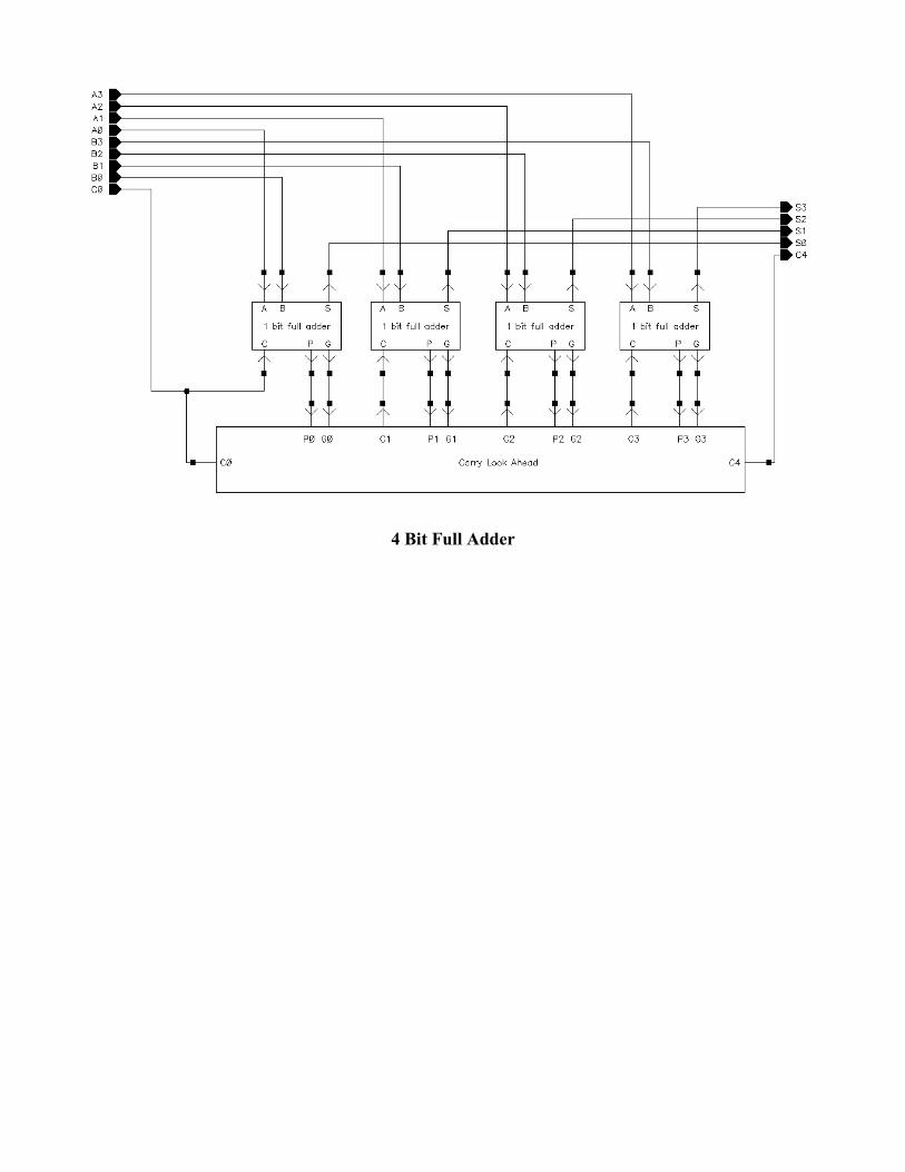
The 12 bit accumulator is composed of 3 4-Full Carry Lookahead Adders (Figure 4). For each bit in a
binary sequence to be added, the Carry Look Ahead Logic will determine whether that bit pair will
generate a carry or propagate a carry. When the actual addition is performed, there is no delay from
waiting for the ripple carry effect.
Figure 4: Four Bit Full Adder
For any circuit larger than 4 bits, the Carry Look Ahead circuitry becomes very complicated and causes
fan-in problems with some gates having more than 5 inputs. The implemented accumulator (Figure 5)
consists of 3 4-Bit Full Adders and latches. Latches are inserted to isolate the adder digital inputs from
the digital outputs when using the adder in the accumulator configuration.
8

Figure 5: 12 Bit Phase Accumulator
As the output frequency is increased, the number of samples per cycle decreases. Since sampling
theory dictates that at least two samples per cycle are required to reconstruct the output waveform, the
maximum fundamental output frequency of a DDS is fC /2. However, for practical applications, the
output frequency is limited to somewhat less than that, improving the quality of the reconstructed
waveform and permitting filtering on the output. When generating a constant frequency, the output of
the phase accumulator increases linearly, so the analog waveform it generates is inherently a ramp.
9

It is important to note that the latch changes its output on the falling edge of the clock cycle which is
not commonly implemented in digital electronics (Figure 6).
Figure 6: 4 Bit Latches
10

3.2 ROM Pointer
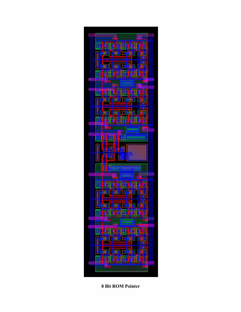
Figure 7: 8 Bit ROM Pointer
The output of the accumulator is fed into 8 Bit ROM pointer shown above (Figure 7) The purpose of
the ROM pointer is to point to the address of a ROM location that contains the correct magnitude of
sine wave.
11

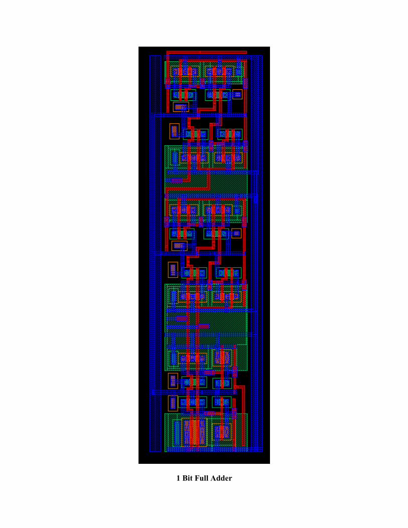
4 LAYOUT
The layout figures shown below display the 12 Bit Phase Accumulator & 8 Bit ROM Pointer (Figure
8) and the complete DDS Layout (Figure 9). Please refer to Appendix B for additional layout figures.
Figure 8: 12 Bit Phase Accumulator & 8 Bit ROM Pointer
Figure 9: Complete DDS Layout
12

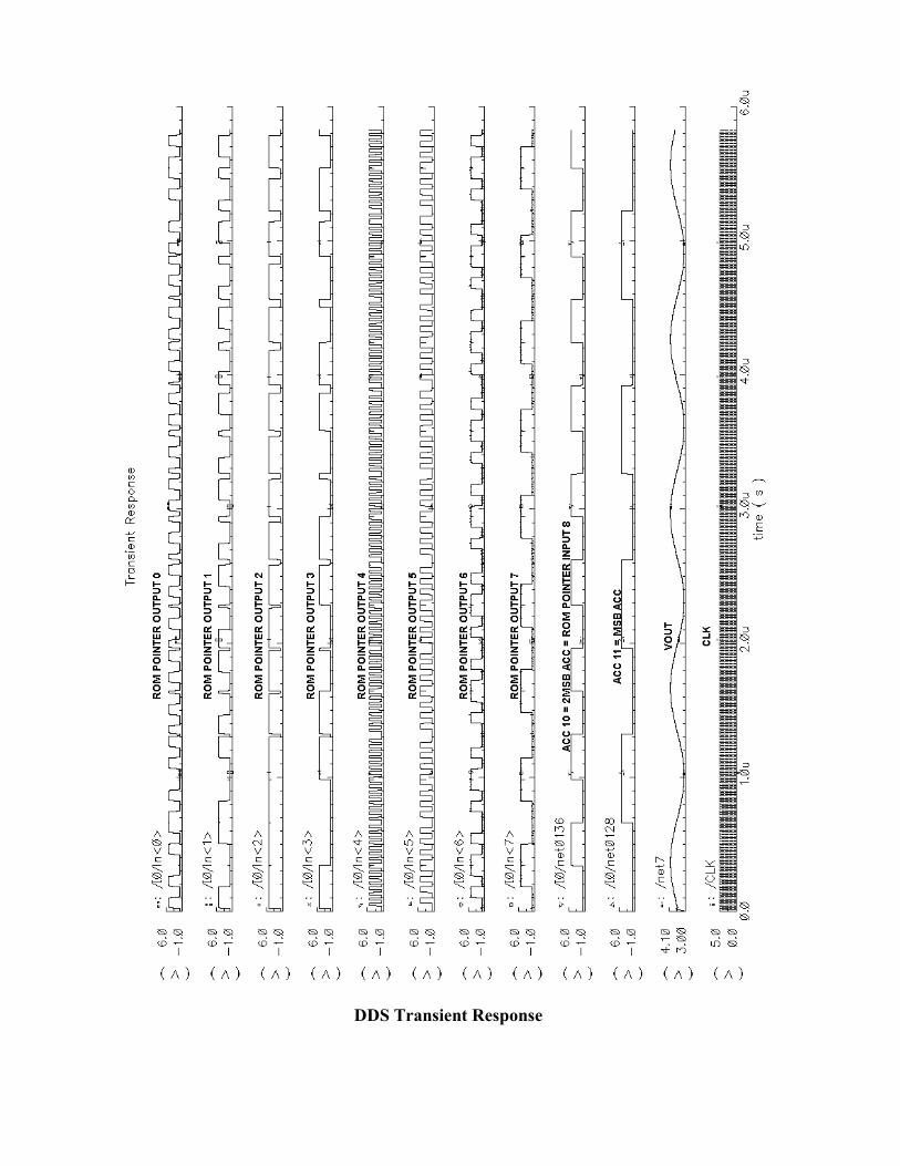
5 SIMULATION
The sample simulation below (Figure 10 & Figure 11) demonstrates the basic operation of DDS.
Please refer to Appendix C for additional simulation results.
Figure 10: DDS Test Bench
Figure 11: DDS Transient Response
13

6. DISCUSSION
Today’s cost-competitive, high-performance, functionally integrated DDS ICs are becoming common
in both communication systems and sensor applications. The advantages that make them attractive to
design engineers include:
• digitally controlled micro-hertz frequency-tuning and sub-degree phase-tuning capability,
• extremely fast hopping speed in tuning output frequency (or phase); phase-continuous frequency hops
with no overshoot/undershoot or analog-related loop settling-time anomalies,
• the digital architecture of DDS eliminates the need for the manual tuning and tweaking related to
component aging and temperature drift in analog synthesizer solutions, and
• the digital control interface of the DDS architecture facilitates an environment where systems can be
remotely controlled and optimized with high resolution under processor control.
14

7 CONCLUSION
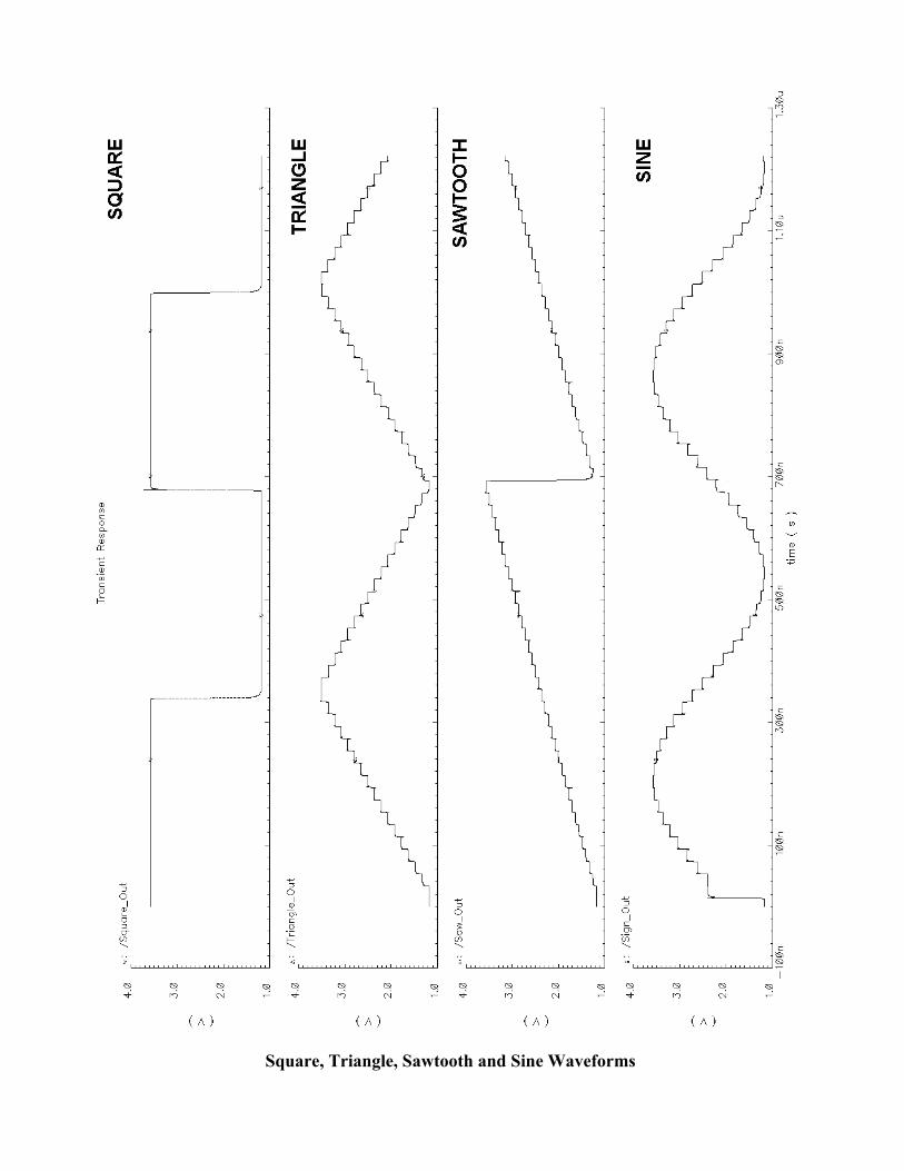
The ability to accurately produce and control waveforms of various frequencies and shapes has become
a key requirement common to a number of industries. Although I was not required to implement
additional waveforms (square, triange, sawtooth) (Figure 12), I was able to simulate them by using
existing DDS blocks. Unfortunately, the chip space and project time did not allow me to make this
additional feature available.
Figure 12: Basic Waveforms produced by rearranging existing DDS building blocks
Taking ECE 547 IC Design/Layout proved to be one of the most exciting learning experiences because
it combined areas covered by many previous undergraduate classes.
15

GLOSSARY OF TERMS:
Amplitude - The maximum absolute value reached by a voltage or current waveform.
Chip - A minute slice of a semiconducting material, such as silicon or germanium, doped and
otherwise processed to have specified electrical characteristics, especially before it is developed into an
electronic component or integrated circuit. Also called microchip.
Clock - A source of regularly occurring pulses used to measure the passage of time, as in a computer.
Digital to Analog Converter (DAC, D/A) - a device for converting a digital (usually binary) code to
an analog signal (current, voltage or charges). Digital-to-Analog Converters are the interface between
the abstract digital world and the analog real life.
Direct Digital Synthesizer (DDS) - Direct Digital Synthesizer (DDS) produces an analog waveform –
usually a sine wave – by generating a time-varying signal in digital form and then performing a digital-
to-analog conversion.
DSP - (Digital Signal Processor) A special-purpose CPU used for digital signal processing
applications. It provides ultra-fast instruction sequences, such as shift and add, and multiply and add,
which are commonly used in math-intensive signal processing.
Latch – an electronic circuit used to store information in asynchronous sequential logic systems.
Modulation - The variation of a property of an electromagnetic wave or signal, such as its amplitude,
frequency, or phase.
Oscillator – an electronic circuit that produces a repetitive electronic signal, often a sine wave or a
square wave.
Phase - The fraction of a complete cycle elapsed as measured from a specified reference point and
often expressed as an angle.
16

Phase Locked Loop - a closed-loop feedback control system that maintains a generated signal in a
fixed phase relationship to a reference signal.
ROM (Read-only memory) - a class of storage media used in computers and other electronic devices
Software Defined Radio – a radio communication system which uses software for the modulation and
demodulation of radio signals.
Synchronous - coordination of occurrences to operate in unison with respect to time.
Waveform – a shape and form of a signal.
17

RESOURCES
Analog Devices Specification Sheet: CMOS DDS Modulator (AD7008 - Rev B)
High Frequency Magazine (Oct. 2004): Low Noise Synthesizers. p. 34, p.44-45
Jouko Vankka1: Direct Digital Synthesizer with an On-Chip D/A Converter Application Note
ADDITIONAL REFERENCES
ROM by Anusha Ramanujam, http://www.eece.maine.edu/vlsi/2006/Ramanujam/
ROM by Cyrus Miller, http://www.eece.maine.edu/vlsi/2006/Miller/
DAC by Raghu Tumati, http://www.eece.maine.edu/vlsi/2006/Tumati/
18

APPENDIX A
SCHEMATICS

Carry 1 Bit Generator
Carry 2 Bit Generator
Carry 2 Bit Generator

Carry 4 Bit Generator

1 Bit Full Adder

4 Bit Full Adder

Carry Lookahead

4 Bit Latch

12 Bit Accumulator

8 Bit ROM Pointer

Complete IC

DDS Test Bench

APPENDIX A
SCHEMATICS

Carry 1 Bit Generator
Carry 2 Bit Generator
Carry 2 Bit Generator

Carry 4 Bit Generator

1 Bit Full Adder
4 Bit Full Adder

Carry Lookahead

4 Bit Latch

12 Bit Accumulator

8 Bit ROM Pointer

Complete IC

DDS Test Bench

APPENDIX B
LAYOUT

1 Bit Full Adder

4 Bit Latch

4 Bit Full Adder with Latches

12 Bit Accumulator

8 Bit ROM Pointer

Complete DDS Layout

APPENDIX C
SIMULATION
DDS Transient Response

Output Voltage Swing with Low Destortion

Output Voltage Swing with Noticeable Distortion

Crossover Distortion

DAC Voltage Stepping

Square, Triangle, Sawtooth and Sine Waveforms

APPENDIX D
MATLAB PROGRAMMING

% Function adder12b takes 2 12-bit words and adds them together. This simulation proves the % functionality of the 12 Bit Adder used in the accumulator configuration.
function [SUM] = adder12b(A , B)
A11 = A(1,1);A10 = A(1,2);A9 = A(1,3);A8 = A(1,4);A7 = A(1,5);A6 = A(1,6);A5 = A(1,7);A4 = A(1,8);A3 = A(1,9);A2 = A(1,10);A1 = A(1,11);A0 = A(1,12);B11 = B(1,1); B10 = B(1,2);B9 = B(1,3);B8 = B(1,4);B7 = B(1,5);B6 = B(1,6);B5 = B(1,7);B4 = B(1,8);B3 = B(1,9);B2 = B(1,10);B1 = B(1,11);B0 = B(1,12);
C0 = 0; % initial carry
G0 = and(A0 , B0);P0 = or(A0 , B0);G1 = and(A1 , B1);P1 = or(A1 , B1);G2 = and(A2 , B2);P2 = or(A2 , B2);G3 = and(A3 , B3);P3 = or(A3 , B3);
G4 = and(A4 , B4);P4 = or(A4 , B4);G5 = and(A5 , B5);P5 = or(A5 , B5);G6 = and(A6 , B6);P6 = or(A6 , B6);G7 = and(A7 , B7);P7 = or(A7 , B7);

G8 = and(A8 , B8);P8 = or(A8 , B8);G9 = and(A9 , B9);P9 = or(A9 , B9);G10 = and(A10 , B10);P10 = or(A10 , B10);G11 = and(A11 , B11);P11 = or(A11 , B11);
% Generate Carry Bits
C1 = or(G0 , and(P0 , C0));C2 = G1 | (P1 & G0) | (P1 & P0 & C0);C3 = G2 | (P2 & G1) | (P2 & P1 & G0) | (P2 & P1 & P0 & C0);C4 = G3 | (P3 & G2) | (P3 & P2 & G1) | (P3 & P2 & P1 & G0) | (P3 & P2 & P1 & P0 & C0);
C5 = or(G4 , and(P4 , C4));C6 = G5 | (P5 & G4) | (P5 & P4 & C4);C7 = G6 | (P6 & G5) | (P6 & P5 & G4) | (P6 & P5 & P4 & C4);C8 = G7 | (P7 & G6) | (P7 & P6 & G5) | (P7 & P6 & P5 & G4) | (P7 & P6 & P5 & P4 & C4);
C9 = or(G8 , and(P8 , C8));C10 = G9 | (P9 & G8) | (P9 & P8 & C8);C11 = G10 | (P10 & G9) | (P10 & P9 & G8) | (P10 & P9 & P8 & C8);C12 = G11 | (P11 & G10) | (P11 & P10 & G9) | (P11 & P10 & P9 & G8) | (P11 & P10 & P9 & P8 & C8);
% Generate Sum Bits
S0 = xor( xor(A0 , B0), C0);S1 = xor( xor(A1 , B1), C1);S2 = xor( xor(A2 , B2), C2);S3 = xor( xor(A3 , B3), C3);
S4 = xor( xor(A4 , B4), C4);S5 = xor( xor(A5 , B5), C5);S6 = xor( xor(A6 , B6), C6);S7 = xor( xor(A7 , B7), C7);
S8 = xor( xor(A8 , B8 ), C8 );S9 = xor( xor(A9 , B9), C9);S10 = xor( xor(A10 , B10), C10);S11 = xor( xor(A11 , B11), C11);
SUM = [S11 S10 S9 S8 S7 S6 S5 S4 S3 S2 S1 S0]CARRY = [C12 C11 C10 C9 C8 C7 C6 C5 C4 C3 C2 C1];
end

% Function flip takes a 12-bit word and performs 1 complement operation depending on the % 2MSB of the accumulator. This simulation proves the functionality of the 8 Bit ROM Pointer.% In the implemented DDS configuration, the last three significant bits are ignored, and one % complement also is not performed on the accumulator MSB and 2MSB bits. % 2MSB is indicated as A(1,2). The least significant bit is A(1,12).
function [B] = flip(A)
B = [ A(1,1) A(1,2) xor(A(1,3) , A(1,2)) xor(A(1,4) , A(1,2)) xor(A(1,5) , A(1,2)) xor(A(1,6) , A(1,2)) xor(A(1,7) , A(1,2)) xor(A(1,8) , A(1,2)) xor(A(1,9) , A(1,2)) xor(A(1,10) , A(1,2)) xor(A(1,11),A(1,2)) xor(A(1,12), A(1,2))]; end

APPENDIX B
LAYOUT
1 Bit Full Adder

4 Bit Latch

4 Bit Full Adder with Latches

12 Bit Accumulator
8 Bit ROM Pointer

Complete DDS Layout

APPENDIX C
SIMULATION

DDS Transient Response

Output Voltage Swing with Low Destortion

Output Voltage Swing with Noticeable Distortion

Crossover Distortion

DAC Voltage Stepping
Square, Triangle, Sawtooth and Sine Waveforms

APPENDIX D
MATLAB PROGRAMMING

% Function adder12b takes 2 12-bit words and adds them together. This simulation proves the % functionality of the 12 Bit Adder used in the accumulator configuration.
function [SUM] = adder12b(A , B)
A11 = A(1,1);A10 = A(1,2);A9 = A(1,3);A8 = A(1,4);A7 = A(1,5);A6 = A(1,6);A5 = A(1,7);A4 = A(1,8);A3 = A(1,9);A2 = A(1,10);A1 = A(1,11);A0 = A(1,12);B11 = B(1,1); B10 = B(1,2);B9 = B(1,3);B8 = B(1,4);B7 = B(1,5);B6 = B(1,6);B5 = B(1,7);B4 = B(1,8);B3 = B(1,9);B2 = B(1,10);B1 = B(1,11);B0 = B(1,12);
C0 = 0; % initial carry
G0 = and(A0 , B0);P0 = or(A0 , B0);G1 = and(A1 , B1);P1 = or(A1 , B1);G2 = and(A2 , B2);P2 = or(A2 , B2);G3 = and(A3 , B3);P3 = or(A3 , B3);
G4 = and(A4 , B4);P4 = or(A4 , B4);G5 = and(A5 , B5);P5 = or(A5 , B5);G6 = and(A6 , B6);P6 = or(A6 , B6);G7 = and(A7 , B7);P7 = or(A7 , B7);

G8 = and(A8 , B8);P8 = or(A8 , B8);G9 = and(A9 , B9);P9 = or(A9 , B9);G10 = and(A10 , B10);P10 = or(A10 , B10);G11 = and(A11 , B11);P11 = or(A11 , B11);
% Generate Carry Bits
C1 = or(G0 , and(P0 , C0));C2 = G1 | (P1 & G0) | (P1 & P0 & C0);C3 = G2 | (P2 & G1) | (P2 & P1 & G0) | (P2 & P1 & P0 & C0);C4 = G3 | (P3 & G2) | (P3 & P2 & G1) | (P3 & P2 & P1 & G0) | (P3 & P2 & P1 & P0 & C0);
C5 = or(G4 , and(P4 , C4));C6 = G5 | (P5 & G4) | (P5 & P4 & C4);C7 = G6 | (P6 & G5) | (P6 & P5 & G4) | (P6 & P5 & P4 & C4);C8 = G7 | (P7 & G6) | (P7 & P6 & G5) | (P7 & P6 & P5 & G4) | (P7 & P6 & P5 & P4 & C4);
C9 = or(G8 , and(P8 , C8));C10 = G9 | (P9 & G8) | (P9 & P8 & C8);C11 = G10 | (P10 & G9) | (P10 & P9 & G8) | (P10 & P9 & P8 & C8);C12 = G11 | (P11 & G10) | (P11 & P10 & G9) | (P11 & P10 & P9 & G8) | (P11 & P10 & P9 & P8 & C8);
% Generate Sum Bits
S0 = xor( xor(A0 , B0), C0);S1 = xor( xor(A1 , B1), C1);S2 = xor( xor(A2 , B2), C2);S3 = xor( xor(A3 , B3), C3);
S4 = xor( xor(A4 , B4), C4);S5 = xor( xor(A5 , B5), C5);S6 = xor( xor(A6 , B6), C6);S7 = xor( xor(A7 , B7), C7);
S8 = xor( xor(A8 , B8 ), C8 );S9 = xor( xor(A9 , B9), C9);S10 = xor( xor(A10 , B10), C10);S11 = xor( xor(A11 , B11), C11);
SUM = [S11 S10 S9 S8 S7 S6 S5 S4 S3 S2 S1 S0]CARRY = [C12 C11 C10 C9 C8 C7 C6 C5 C4 C3 C2 C1];
end

% Function flip takes a 12-bit word and performs 1 complement operation depending on the % 2MSB of the accumulator. This simulation proves the functionality of the 8 Bit ROM Pointer.% In the implemented DDS configuration, the last three significant bits are ignored, and one % complement also is not performed on the accumulator MSB and 2MSB bits. % 2MSB is indicated as A(1,2). The least significant bit is A(1,12).
function [B] = flip(A)
B = [ A(1,1) A(1,2) xor(A(1,3) , A(1,2)) xor(A(1,4) , A(1,2)) xor(A(1,5) , A(1,2)) xor(A(1,6) , A(1,2)) xor(A(1,7) , A(1,2)) xor(A(1,8) , A(1,2)) xor(A(1,9) , A(1,2)) xor(A(1,10) , A(1,2)) xor(A(1,11),A(1,2)) xor(A(1,12), A(1,2))]; end