direct imaging of the near field and dynamics of … for use title direct imaging of the near field...
TRANSCRIPT

Instructions for use
Title Direct imaging of the near field and dynamics of surface plasmon resonance on gold nanostructures usingphotoemission electron microscopy
Author(s) Sun, Quan; Ueno, Kosei; Yu, Han; Kubo, Atsushi; Matsuo, Yasutaka; Misawa, Hiroaki
Citation Light : science & applications, 2: e118-1-e118-8
Issue Date 2013-12
Doc URL http://hdl.handle.net/2115/54783
Rights(URL) http://creativecommons.org/licenses/by-nc-sa/3.0/
Type article
File Information lsa201374a.pdf
Hokkaido University Collection of Scholarly and Academic Papers : HUSCAP
ORIGINAL ARTICLE
Direct imaging of the near field and dynamics of surfaceplasmon resonance on gold nanostructures usingphotoemission electron microscopy
Quan Sun1,2, Kosei Ueno1,3, Han Yu1, Atsushi Kubo4, Yasutaka Matsuo1 and Hiroaki Misawa1
Localized surface plasmon resonance (LSPR) can be supported by metallic nanoparticles and engineered nanostructures. An
understanding of the spatially resolved near-field properties and dynamics of LSPR is important, but remains experimentally
challenging. We report experimental studies toward this aim using photoemission electron microscopy (PEEM) with high spatial
resolution of sub-10 nm. Various engineered gold nanostructure arrays (such as rods, nanodisk-like particles and dimers) are
investigated via PEEM using near-infrared (NIR) femtosecond laser pulses as the excitation source. When the LSPR wavelengths
overlap the spectrum of the femtosecond pulses, the LSPR is efficiently excited and promotes multiphoton photoemission, which is
correlated with the local intensity of the metallic nanoparticles in the near field. Thus, the local field distribution of the LSPR on
different Au nanostructures can be directly explored and discussed using the PEEM images. In addition, the dynamics of the LSPR is
studied by combining interferometric time-resolved pump-probe technique and PEEM. Detailed information on the oscillation and
dephasing of the LSPR field can be obtained. The results identify PEEM as a powerful tool for accessing the near-field mapping and
dynamic properties of plasmonic nanostructures.
Light: Science & Applications (2013) 2, e118; doi:10.1038/lsa.2013.74; published online 20 December 2013
Keywords: femtosecond laser; local field enhancement; near-field imaging; photoemission electron microscopy; surface plasmonresonance
INTRODUCTION
Because of the rapid development of nanofabrication techniques,
metallic nanostructures that can exhibit localized surface plasmon
resonance (LSPR) can be fabricated using several methods. The re-
sonance frequency and amplitude of LSPR on metallic nanostructures
are known to depend on the metal materials, shapes, and surrounding
media.1–4 In addition, the LSPR can confine optical fields in nanoscale
space, leading to the so-called local field enhancement effect. These
unique properties promote the application of LSPR in many fields,
such as surface-enhanced Raman scattering,5–8 sensing,1,9,10 plasmon-
assisted photochemical reactions4,11,12 and photocurrent genera-
tion.13–15 To further understand the LSPR mechanism and to optimize
the design of the plasmonic nanostructures for most applications, the
near-field properties of the LSPR fields (especially the near-field dis-
tribution of the plasmonic nanostructures) must be determined. To
date, investigations of the optical properties of LSPR have largely
relied on far-field spectroscopic techniques or numerical simulations.
Several experimental approaches have been utilized to visualize the
near field, including scanning photoionization microscopy,16,17 scan-
ning near-field optical microscopy,18–21 nonlinear luminescence or
fluorescent microscopy,22,23 nonlinear photopolymerization24,25 and
near-field ablation of a substrate.26–29 However, these approaches have
practical limitations; specifically, both scanning photoionization
microscopy and scanning near-field optical microscopy require a
scanning process to acquire a near-field image, and their spatial reso-
lution barely reaches the sub-50-nm level. Only a limited study has
demonstrated sub-10 nm resolution in imaging metal nanogaps using
a scattering-type scanning near-field optical microscopy.21 Nonlinear
fluorescence microscopy and photopolymerization require special
treatment of the investigated samples; the metallic nanostructures
must be coated with a layer of dye material or photopolymers. This
additional layer also alters the properties of the LSPR. The near-field
ablation technique imposes permanent damage onto the samples.
Therefore, directly imaging the near fields of plasmonic nano-
structures with high spatial resolution remains an experimental chal-
lenge. Understanding the dynamic properties of the LSPR is also
highly desired, but rarely realized experimentally.
The recent development of multiphoton photoemission electron
microscopy (MP-PEEM) has resulted in a novel approach to directly
visualize the near-field of LSPR supported on metallic nano-
structures.30–35 Photoemission electron microscopy records the elec-
trons emitted from a sample in response to the absorption of incident
photons. Conventional PEEM uses ultraviolet (UV) light or X-ray
radiation as the excitation source and has been demonstrated as a
1Research Institute for Electronic Science, Hokkaido University, Sapporo 001-0021, Japan; 2Creative Research Institution, Hokkaido University, Sapporo 001-0021, Japan;3PRESTO, Japan Science and Technology Agency, Kawaguchi 332-0012, Japan and 4Institute of Physics, University of Tsukuba, Tsukuba 305-8571, JapanCorrespondence: Professor H Misawa, Research Institute for Electronic Science, Hokkaido University, Sapporo 001-0021, JapanE-mail: [email protected]
Received 11 March 2013; revised 12 June 2013; accepted 16 August 2013
OPENLight: Science & Applications (2013) 2, e118; doi:10.1038/lsa.2013.74� 2013 CIOMP. All rights reserved 2047-7538/13
www.nature.com/lsa
powerful imaging and characterization tool in the fields of surface
physics/chemistry, material growth and magnetic materials.36,37 In
contrast to scanning electron microscopy, PEEM can directly image
surface areas emitting photoelectrons in real time without scanning.
MP-PEEM is based on the multiphoton photoemission from a species
excited by ultrashort (picosecond or femtosecond) laser pulses. The
probability of multiphoton excitation is typically low; however, LSPR-
assisted local field enhancement can promote the multiphoton excita-
tion of metallic nanostructures and render MP-PEEM suitable for
direct imaging of the near-field LSPR. The combination of MP-
PEEM with pump-probe techniques, namely, time-resolved MP-
PEEM (TR-MP-PEEM),32,38,39 was established to investigate the
dynamics of LSPR and the propagating surface plasmon polariton.
Two-photon PEEM investigations have typically been performed on
Ag nanostructures excited by near-ultraviolet femtosecond laser
pulses (,400 nm, double frequency of a Ti:sapphire laser).30–32 The
LSPR of the Au nanoparticles lies in visible region (,510 nm) and
near-infrared (NIR) region so that it cannot be excited by near-ultra-
violet light. For example, the LSPR wavelength of the Au nano-
structures studied in this paper is in the range of 700–900 nm,
which is far from the double frequency of Ti:sapphire laser pulses.
Therefore, the fundamental frequency of Ti:sapphire femtosecond
laser pulses should be more suitable for exciting such LSPR modes.
However, only few reports have described investigations of the LSPR
using MP-PEEM with femtosecond pulses from an 800-nm excitation
source,33–35 likely because of the difficulty in achieving higher non-
linear photoemission. Furthermore, no reports have yet described the
direct observation of the dynamics of LSPR on Au nanoparticles using
TR-MP-PEEM at this wavelength.
In this study, we established an MP-PEEM system using NIR ultra-
short femtosecond laser pulses as the excitation source. We used the
system to directly image the near field of LSPR on various Au nano-
particle arrays. The wide bandwidth (ranging from 650–1050 nm) of
the laser pulses allowed excitation of the LSPR over a wide spectral
region under resonance or near-resonance conditions. The near-field
mapping and the local field enhancement sites can be precisely
obtained because of the high spatial resolution of PEEM (,8 nm),
which enable us to visualize polarization distribution in a metal nanos-
tructure or an aggregate of nanostructures. It is worth mentioning that
in the most case of plasmon imaging by PEEM, the spatial resolution
has been limited to ,50 nm.30,32,33,35,38 The ultrashort pulse duration
(7 fs) makes this light source suitable for time-resolved studies. We
also combined MP-PEEM with an interferometric time-resolved
photoemission technique to establish a TR-MP-PEEM system to
investigate the dynamics of the LSPR. This paper is organized as fol-
lows. First, we report the near-field mapping of three different Au
nanoparticle arrays via MP-PEEM. For complicated structures in par-
ticular (using dimers as an example), the local field enhancement sites
can be directly visualized by simultaneous irradiation with NIR fem-
tosecond pulses and UV light. Second, we present dynamics studies of
the LSPR via TR-MP-PEEM. The oscillation and dephasing of the
LSPR fields in the NIR region on the Au nanoparticles were observed
using this time-resolved technique for the first time. In particular, we
demonstrated the ability of the TR-MP-PEEM technique to resolve
two different LSPR frequencies.
MATERIALS AND METHODS
To fabricate the gold nanoparticle arrays, we applied electron-beam
lithography followed by metal sputtering and lift-off techniques. The
fabrication procedure used in this study was similar to the process
described in our earlier reports.22,25 Patterns of Au nanostructures
were formed on Nb-doped TiO2 (110) substrates that were designed
using a high-resolution electron-beam lithography system (ELS-F125;
Elionix, Tokyo, Japan) operating at 125 kV. A conventional copolymer
resist (ZEP520A; Zeon Chemicals, Louisville, USA) diluted with a ZEP
thinner (1 : 1) was spin-coated onto the substrate at 1000 r.p.m. for 10 s
and 4000 r.p.m. for 90 s, and it was then prebaked on a hot plate for
2 min at 150 6C. The electron-beam lithography operated at an elec-
trical current of 3 nA. After development, a 2-nm-thick titanium layer
was first deposited via sputtering (MPS-4000; ULVAC, Tokyo, Japan)
as the adhesive layer, followed by a 40-nm-thick gold film. The lift-off
was performed by successively immersing the sample in anisole, acet-
one and ultrapure water in an ultrasonic bath. Four differently shaped
Au nanoparticle arrays were utilized in this study, namely, nanorods
(rectangular), nanodisk-like particles (round), dimers and nanoblocks
(square), and were arranged in two-dimensional arrays on the sub-
strates. Field-emission scanning electron microscopy (JSM-6700FT;
JEOL, Tokyo, Japan) and Fourier transform infrared (FTIR) spectro-
scopy (FT/IR-6000TM-M; JASCO, Tokyo, Japan) were used to char-
acterize the morphologies and far-field spectral properties of the Au
nanostructures, respectively.
The photoemission electron microscope used in this study was a
PEEM with an energy analyzer (Elmitec GmbH, Clausthal-Zellerfeld,
Germany) with a spatial resolution of over 8 nm. As an excitation
source, we used either a mercury lamp (unpolarized continuous wave
light with a cutoff energy of 4.9 eV) or a mode-locked Ti:sapphire
oscillator (Rainbow; Femtolasers, Vienna, Austria) that delivered a
7-fs laser pulse at a central wavelength of 800 nm with a .200-nm
bandwidth at a repetition rate of 77 MHz. The sample was irradiated at
an angle of 746. The femtosecond laser beam was focused down to a
spot of approximately 50 mm3200 mm on the sample using a lens
(focal length f5150 mm). Chirp mirror pairs and a wedge pair were
used to compensate for the dispersion to obtain the shortest pulse
duration inside the PEEM chamber. The polarization of the laser beam
was controlled by a l/2 waveplate, and a p-polarized beam was used in
this study. The interferometric time-resolved setup was based on a
Mach-Zehnder interferometer. Typically, time-resolved PEEM images
can be recorded by adjusting the delay time at a step corresponding to
a p/2 phase delay (for a carrier wavelength of 800 nm, is 0.67 fs).
RESULTS AND DISCUSSION
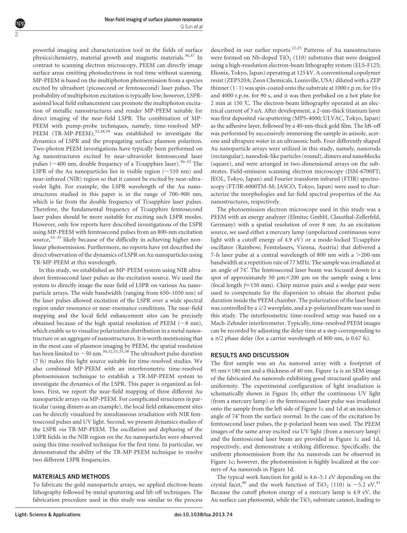
The first sample was an Au nanorod array with a footprint of
95 nm3180 nm and a thickness of 40 nm. Figure 1a is an SEM image
of the fabricated Au nanorods exhibiting good structural quality and
uniformity. The experimental configuration of light irradiation is
schematically shown in Figure 1b; either the continuous UV light
(from a mercury lamp) or the femtosecond laser pulse was irradiated
onto the sample from the left side of Figure 1c and 1d at an incidence
angle of 746 from the surface normal. In the case of the excitation by
femtosecond laser pulses, the p-polarized beam was used. The PEEM
images of the same array excited via UV light (from a mercury lamp)
and the femtosecond laser beam are provided in Figure 1c and 1d,
respectively, and demonstrate a striking difference. Specifically, the
uniform photoemission from the Au nanorods can be observed in
Figure 1c; however, the photoemission is highly localized at the cor-
ners of Au nanorods in Figure 1d.
The typical work function for gold is 4.6–5.1 eV depending on the
crystal facet,40 and the work function of TiO2 (110) is ,5.2 eV.41
Because the cutoff photon energy of a mercury lamp is 4.9 eV, the
Au surface can photoemit, while the TiO2 substrate cannot, leading to
Near-field imaging of surface plasmon resonance
Q Sun et al
2
Light: Science & Applications doi:10.1038/lsa.2013.74
the image contrast in Figure 1c that results from the difference in the
work function. For the femtosecond laser pulses, a one-photon energy
is insufficient to overcome the work function and emit electrons.
However, the Au nanorods can support two LSPR modes: one is a
longitudinal plasmon mode (L-mode) with the polarization parallel to
the long axes of the nanorods, and the other is transverse plasmon
mode (T-mode) with the polarization parallel to the short axes of the
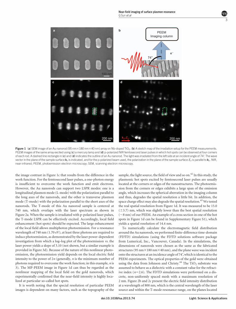
nanorods. The T-mode of this Au nanorod sample is centered at
740 nm, which overlaps with the laser spectrum as shown in
Figure 2a. When the sample is irradiated with p-polarized laser pulses,
the T-mode LSPR can be effectively excited. Accordingly, local field
enhancement (hot spots) should be expected. The large enhancement
of the local field allows multiphoton photoemission. For a resonance
wavelength of 740 nm (1.70 eV), at least three photons are required to
induce photoemission, as demonstrated by the laser power-dependent
investigation from which a log–log plot of the photoemission vs. the
laser power yields a slope of 3.10 (not shown, but a similar example is
provided in Figure 3d). Because of the nature of this nonlinear photo-
emission, the photoemission yield depends on the local electric field
intensity to the power of 2n (generally, n is the minimum number of
photons required to overcome the work function; in this example, n is
3). The MP-PEEM image in Figure 1d can thus be regarded as the
nonlinear mapping of the local field on the gold nanorods, which
experimentally confirmed that the near-field intensity is highly loca-
lized at particular so-called hot spots.
It is worth noting that the special resolution of particular PEEM
images is dependent on many factors, such as the topography of the
sample, the light source, the field of view and so on.42 In this study, the
plasmonic hot spots excited by femtosecond laser pulses are usually
located at the corners or edges of the nanostructures. The photoemis-
sion from the corners or edges exhibits a large span of the emission
angle, which increases the spherical aberration in the imaging column
and thus, degrades the spatial resolution a little bit. In addition, the
space charge effect may also degrade the spatial resolution.43 We tested
the real spatial resolution from Figure 1d. It was measured to be 15.0
(63.7) nm, which was slightly lower than the best spatial resolution
(,8 nm) of our PEEM. An example of a cross section in one of the hot
spots in Figure 1d can be found in Supplementary Figure S1), which
yields a spatial resolution of 14.4 nm.
To numerically calculate the electromagnetic field distribution
around the Au nanorods, we performed finite-difference time-domain
(FDTD) simulations (using the FDTD solutions software package
from Lumerical, Inc., Vancouver, Canada). In the simulations, the
dimensions of nanorods were chosen as the same as the fabricated
structures (95 nm3180 nm340 nm), and the plane wave was incident
onto the structures at an incidence angle of 746, which is identical to the
PEEM experiments. The optical properties of the gold were obtained
using the data from Johnson and Christy.44 The TiO2 substrate was
assumed to behave as a dielectric with a constant value for the refract-
ive index (n52.6). The FDTD simulations were performed on a dis-
crete, non-uniformly spaced mesh with a maximum resolution of
2 nm. Figure 2b and 2c present the electric field intensity distribution
at a wavelength of 800 nm, which is the central wavelength of the laser
source and within the T-mode resonance range, on the planes located
a
c
b PEEMImaging column
74°
200 nm
100 nm
200 nmk//,E//
e_
d
Figure 1 (a) SEM image of an Au nanorod (95 nm3180 nm340 nm) array on Nb-doped TiO2. (b) A sketch map of the irradiation setup for the PEEM measurements.
PEEM images of the same array excited using (c) a mercury lamp and (d) p-polarized NIR femtosecond laser pulses in which hot spots can be observed at four corners
of each rod. A dashed line rectangle in (c) and (d) indicates the outline of an Au nanorod. The light was irradiated from the left side at an incident angle of 746. The wave
vector in the plane of the sample surface k// is indicated, and for the p-polarized beam used, the polarization in the plane of the sample surface E// is parallel to k//. NIR,
near-infrared; PEEM, photoemission electron microscopy; SEM, scanning electron microscopy.
Near-field imaging of surface plasmon resonanceQ Sun et al
3
doi:10.1038/lsa.2013.74 Light: Science & Applications
at the top and bottom of the Au nanorods, respectively. For both
planes, the calculations of the field intensity distribution are in good
agreement with the experimental results obtained from the PEEM
measurements with the resonant femtosecond laser pulse excitation.
The peak enhancement on the bottom plane was much greater than
that on the top plane, as predicted by the simulations. However, val-
idating this result using the PEEM measurements is difficult because
the photoemissions from different vertical positions are difficult to
distinguish. For most nanorods, the hot spots at the right corners of the
rods are brighter than those at the left corners. This phenomenon was
also well reproduced by the simulations and is attributed to the retarda-
tion effect33 because the light was irradiated from the left side at a
grazing angle. So far, the highly spatially resolved near-field mapping
of the LSPR field on the Au nanorods was successfully obtained with
the PEEM measurements using femtosecond laser pulse irradiation
through nonlinear photoemission.
As previously mentioned, the wavelength and amplitude of the
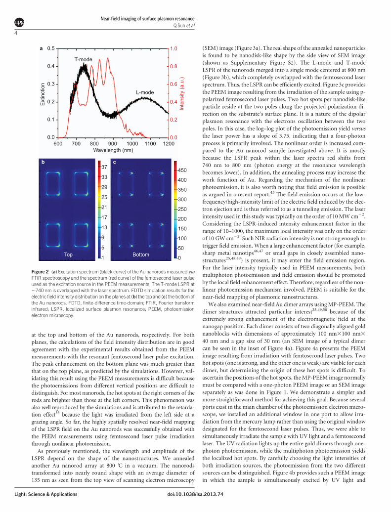
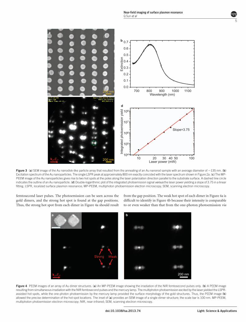
LSPR depend on the shape of the nanostructures. We annealed
another Au nanorod array at 800 6C in a vacuum. The nanorods
transformed into nearly round shape with an average diameter of
135 nm as seen from the top view of scanning electron microscopy
(SEM) image (Figure 3a). The real shape of the annealed nanoparticles
is found to be nanodisk-like shape by the side view of SEM image
(shown as Supplementary Figure S2). The L-mode and T-mode
LSPR of the nanorods merged into a single mode centered at 800 nm
(Figure 3b), which completely overlapped with the femtosecond laser
spectrum. Thus, the LSPR can be efficiently excited. Figure 3c provides
the PEEM image resulting from the irradiation of the sample using p-
polarized femtosecond laser pulses. Two hot spots per nanodisk-like
particle reside at the two poles along the projected polarization di-
rection on the substrate’s surface plane. It is a nature of the dipolar
plasmon resonance with the electrons oscillation between the two
poles. In this case, the log–log plot of the photoemission yield versus
the laser power has a slope of 3.75, indicating that a four-photon
process is primarily involved. The nonlinear order is increased com-
pared to the Au nanorod sample investigated above. It is mostly
because the LSPR peak within the laser spectra red shifts from
740 nm to 800 nm (photon energy at the resonance wavelength
becomes lower). In addition, the annealing process may increase the
work function of Au. Regarding the mechanism of the nonlinear
photoemission, it is also worth noting that field emission is possible
as argued in a recent report.45 The field emission occurs at the low-
frequency/high-intensity limit of the electric field induced by the elec-
tron ejection and is thus referred to as a tunneling emission. The laser
intensity used in this study was typically on the order of 10 MW cm22.
Considering the LSPR-induced intensity enhancement factor in the
range of 10–1000, the maximum local intensity was only on the order
of 10 GW cm22. Such NIR radiation intensity is not strong enough to
trigger field emission. When a large enhancement factor (for example,
sharp metal nanotips46,47 or small gaps in closely assembled nano-
structures25,48,49) is present, it may enter the field emission region.
For the laser intensity typically used in PEEM measurements, both
multiphoton photoemission and field emission should be promoted
by the local field enhancement effect. Therefore, regardless of the non-
linear photoemission mechanism involved, PEEM is suitable for the
near-field mapping of plasmonic nanostructures.
We also examined near-field Au dimer arrays using MP-PEEM. The
dimer structures attracted particular interest25,49,50 because of the
extremely strong enhancement of the electromagnetic field at the
nanogap position. Each dimer consists of two diagonally aligned gold
nanoblocks with dimensions of approximately 100 nm3100 nm3
40 nm and a gap size of 30 nm (an SEM image of a typical dimer
can be seen in the inset of Figure 4a). Figure 4a presents the PEEM
image resulting from irradiation with femtosecond laser pulses. Two
hot spots (one is strong, and the other one is weak) are visible for each
dimer, but determining the origin of these hot spots is difficult. To
ascertain the positions of the hot spots, the MP-PEEM image normally
must be compared with a one-photon PEEM image or an SEM image
separately as was done in Figure 1. We demonstrate a simpler and
more straightforward method for achieving this goal. Because several
ports exist in the main chamber of the photoemission electron micro-
scope, we installed an additional window in one port to allow irra-
diation from the mercury lamp rather than using the original window
designated for the femtosecond laser pulses. Thus, we were able to
simultaneously irradiate the sample with UV light and a femtosecond
laser. The UV radiation lights up the entire gold dimers through one-
photon photoemission, while the multiphoton photoemission yields
the localized hot spots. By carefully choosing the light intensities of
both irradiation sources, the photoemission from the two different
sources can be distinguished. Figure 4b provides such a PEEM image
in which the sample is simultaneously excited by UV light and
0.4
0.3
Ext
inct
ion
0.2
0.1
0.5
T-mode
L-mode
0.011001000900
Wavelength (nm)
Top Bottom
800700600 1200
400
350
300
250
200
150
100
50
450
0
33
29
25
21
17
13
9
5
37
1
0.8
0.6
Inte
nsity
(a.u
.)
0.4
0.2
1.0
0.0
b c
a
Figure 2 (a) Excitation spectrum (black curve) of the Au nanorods measured via
FTIR spectroscopy and the spectrum (red curve) of the femtosecond laser pulse
used as the excitation source in the PEEM measurements. The T-mode LSPR at
,740 nm is overlapped with the laser spectrum. FDTD simulation results for the
electric field intensity distribution on the planes at (b) the top and (c) the bottom of
the Au nanorods. FDTD, finite-difference time-domain; FTIR, Fourier transform
infrared; LSPR, localized surface plasmon resonance; PEEM, photoemission
electron microscopy.
Near-field imaging of surface plasmon resonance
Q Sun et al
4
Light: Science & Applications doi:10.1038/lsa.2013.74
femtosecond laser pulses. The photoemission can be seen across the
gold dimers, and the strong hot spot is found at the gap positions.
Thus, the strong hot spot from each dimer in Figure 4a should result
from the gap position. The weak hot spot of each dimer in Figure 4a is
difficult to identify in Figure 4b because their intensity is comparable
to or even weaker than that from the one-photon photoemission via
dc
a
b
0.6
0.5
0.4
0.3
0.2
0.1
0.0
0.7
Ext
inct
ion
11001000900Wavelength (nm)
Inte
grat
ed p
hoto
emis
sion
yie
ld
Laser power (mW)
Slope=3.75
5040302010 100
800700
107
106
105
108
104
k//,E//
200 nm
200 nm
Figure 3 (a) SEM image of the Au nanodisk-like particle array that resulted from the annealing of an Au nanorod sample with an average diameter of ,135 nm. (b)
Excitation spectrum of the Au nanoparticles. The single LSPR peak at approximately 800 nm exactly coincided with the laser spectrum shown in Figure 2a. (c) The MP-
PEEM image of the Au nanoparticles gives rise to two hot spots at the poles along the laser polarization direction parallel to the substrate surface. A dashed line circle
indicates the outline of an Au nanoparticle. (d) Double-logarithmic plot of the integrated photoemission signal versus the laser power yielding a slope of 3.75 in a linear
fitting. LSPR, localized surface plasmon resonance; MP-PEEM, multiphoton photoemission electron microscopy; SEM, scanning electron microscopy.
a b
k//,E//
Strong Weak
200 nm
Figure 4 PEEM images of an array of Au dimer structures. (a) An MP-PEEM image showing the irradiation of the NIR femtosecond pulses only. (b) A PEEM image
resulting from simultaneous irradiation with the NIR femtosecond pulses and the mercury lamp. The multiphoton photoemission excited by the laser yielded the LSPR-
assisted hot spots, while the one-photon photoemission by the mercury lamp provided the surface morphology of the gold structures. Thus, the PEEM image (b)
allowed the precise determination of the hot spot locations. The inset of (a) provides an SEM image of a single dimer structure; the scale bar is 100 nm. MP-PEEM,
multiphoton photoemission electron microscopy; NIR, near-infrared; SEM, scanning electron microscopy.
Near-field imaging of surface plasmon resonanceQ Sun et al
5
doi:10.1038/lsa.2013.74 Light: Science & Applications
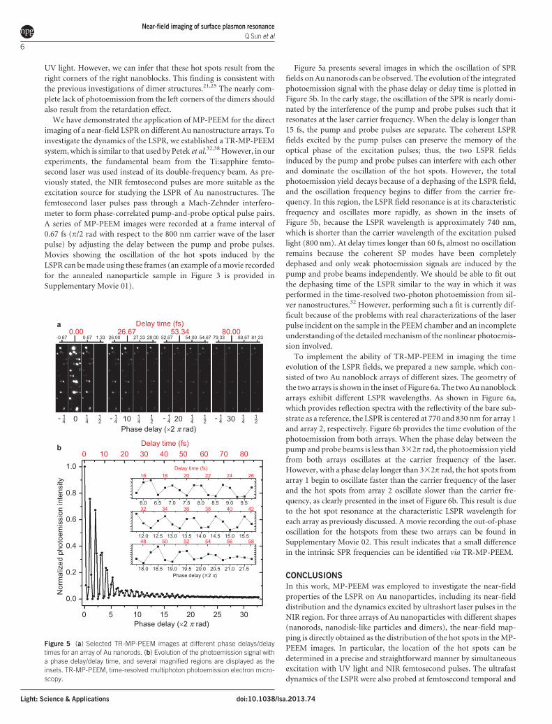
UV light. However, we can infer that these hot spots result from the
right corners of the right nanoblocks. This finding is consistent with
the previous investigations of dimer structures.21,25 The nearly com-
plete lack of photoemission from the left corners of the dimers should
also result from the retardation effect.
We have demonstrated the application of MP-PEEM for the direct
imaging of a near-field LSPR on different Au nanostructure arrays. To
investigate the dynamics of the LSPR, we established a TR-MP-PEEM
system, which is similar to that used by Petek et al.32,38 However, in our
experiments, the fundamental beam from the Ti:sapphire femto-
second laser was used instead of its double-frequency beam. As pre-
viously stated, the NIR femtosecond pulses are more suitable as the
excitation source for studying the LSPR of Au nanostructures. The
femtosecond laser pulses pass through a Mach-Zehnder interfero-
meter to form phase-correlated pump-and-probe optical pulse pairs.
A series of MP-PEEM images were recorded at a frame interval of
0.67 fs (p/2 rad with respect to the 800 nm carrier wave of the laser
pulse) by adjusting the delay between the pump and probe pulses.
Movies showing the oscillation of the hot spots induced by the
LSPR can be made using these frames (an example of a movie recorded
for the annealed nanoparticle sample in Figure 3 is provided in
Supplementary Movie 01).
Figure 5a presents several images in which the oscillation of SPR
fields on Au nanorods can be observed. The evolution of the integrated
photoemission signal with the phase delay or delay time is plotted in
Figure 5b. In the early stage, the oscillation of the SPR is nearly domi-
nated by the interference of the pump and probe pulses such that it
resonates at the laser carrier frequency. When the delay is longer than
15 fs, the pump and probe pulses are separate. The coherent LSPR
fields excited by the pump pulses can preserve the memory of the
optical phase of the excitation pulses; thus, the two LSPR fields
induced by the pump and probe pulses can interfere with each other
and dominate the oscillation of the hot spots. However, the total
photoemission yield decays because of a dephasing of the LSPR field,
and the oscillation frequency begins to differ from the carrier fre-
quency. In this region, the LSPR field resonance is at its characteristic
frequency and oscillates more rapidly, as shown in the insets of
Figure 5b, because the LSPR wavelength is approximately 740 nm,
which is shorter than the carrier wavelength of the excitation pulsed
light (800 nm). At delay times longer than 60 fs, almost no oscillation
remains because the coherent SP modes have been completely
dephased and only weak photoemission signals are induced by the
pump and probe beams independently. We should be able to fit out
the dephasing time of the LSPR similar to the way in which it was
performed in the time-resolved two-photon photoemission from sil-
ver nanostructures.32 However, performing such a fit is currently dif-
ficult because of the problems with real characterizations of the laser
pulse incident on the sample in the PEEM chamber and an incomplete
understanding of the detailed mechanism of the nonlinear photoemis-
sion involved.
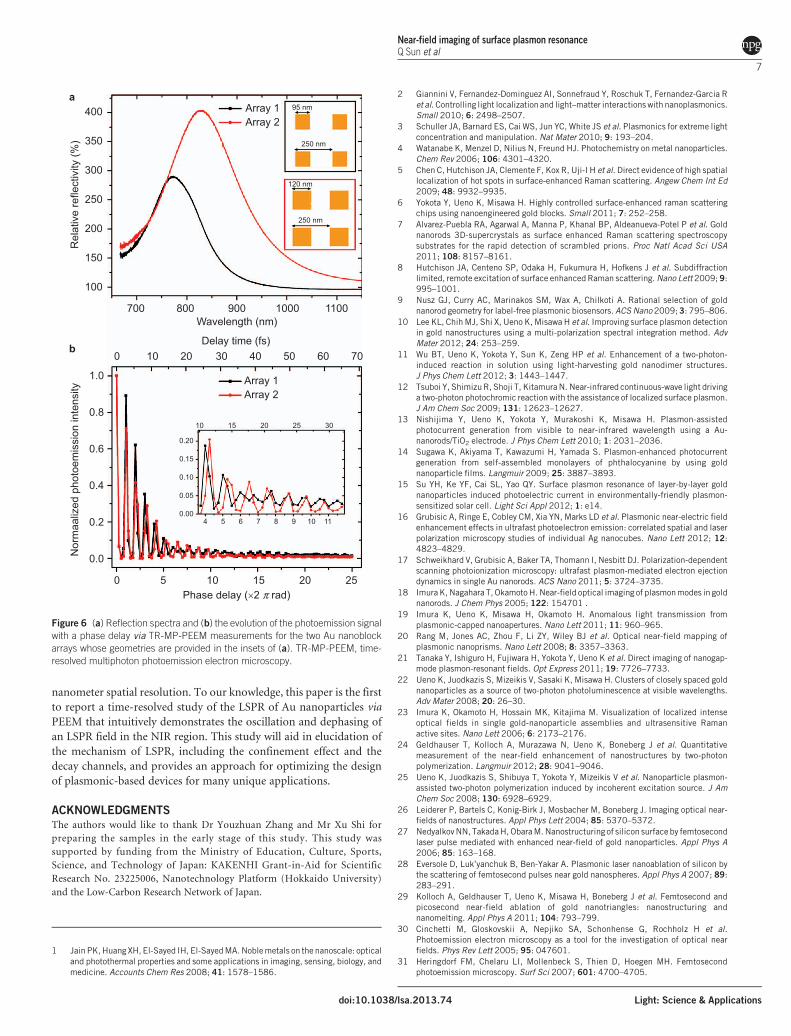
To implement the ability of TR-MP-PEEM in imaging the time
evolution of the LSPR fields, we prepared a new sample, which con-
sisted of two Au nanoblock arrays of different sizes. The geometry of
the two arrays is shown in the inset of Figure 6a. The two Au nanoblock
arrays exhibit different LSPR wavelengths. As shown in Figure 6a,
which provides reflection spectra with the reflectivity of the bare sub-
strate as a reference, the LSPR is centered at 770 and 830 nm for array 1
and array 2, respectively. Figure 6b provides the time evolution of the
photoemission from both arrays. When the phase delay between the
pump and probe beams is less than 332p rad, the photoemission yield
from both arrays oscillates at the carrier frequency of the laser.
However, with a phase delay longer than 332p rad, the hot spots from
array 1 begin to oscillate faster than the carrier frequency of the laser
and the hot spots from array 2 oscillate slower than the carrier fre-
quency, as clearly presented in the inset of Figure 6b. This result is due
to the hot spot resonance at the characteristic LSPR wavelength for
each array as previously discussed. A movie recording the out-of-phase
oscillation for the hotspots from these two arrays can be found in
Supplementary Movie 02. This result indicates that a small difference
in the intrinsic SPR frequencies can be identified via TR-MP-PEEM.
CONCLUSIONS
In this work, MP-PEEM was employed to investigate the near-field
properties of the LSPR on Au nanoparticles, including its near-field
distribution and the dynamics excited by ultrashort laser pulses in the
NIR region. For three arrays of Au nanoparticles with different shapes
(nanorods, nanodisk-like particles and dimers), the near-field map-
ping is directly obtained as the distribution of the hot spots in the MP-
PEEM images. In particular, the location of the hot spots can be
determined in a precise and straightforward manner by simultaneous
excitation with UV light and NIR femtosecond pulses. The ultrafast
dynamics of the LSPR were also probed at femtosecond temporal and
a
b
Delay time (fs)0.00
0 10Phase delay (×2 π rad)
Phase delay (×2 π rad)
Phase delay (×2 π)
Delay time (fs)
Delay time (fs)2422201816 26
4038363432 42
5654525048 58
20 30
-0.67
4- 1 4- 14 1 2 1 4- 14 1 2 1 4- 14 1 2 1 4 1 2 1
0.67 1.33 26.00 27.33 28.00 52.67 54.00 54.67 79.33 81.3380.6726.67 53.34 80.00
0.8
0.6
Nor
mal
ized
pho
toem
issi
on in
tens
ity
0.4
0.2
1.0
9.08.58.07.57.06.56.0 9.5
15.014.514.013.513.012.512.0 15.5
21.020.520.019.519.018.518.0 21.5
0.0
2520151050 30
60504020 30100 8070
Figure 5 (a) Selected TR-MP-PEEM images at different phase delays/delay
times for an array of Au nanorods. (b) Evolution of the photoemission signal with
a phase delay/delay time, and several magnified regions are displayed as the
insets. TR-MP-PEEM, time-resolved multiphoton photoemission electron micro-
scopy.
Near-field imaging of surface plasmon resonance
Q Sun et al
6
Light: Science & Applications doi:10.1038/lsa.2013.74
nanometer spatial resolution. To our knowledge, this paper is the first
to report a time-resolved study of the LSPR of Au nanoparticles via
PEEM that intuitively demonstrates the oscillation and dephasing of
an LSPR field in the NIR region. This study will aid in elucidation of
the mechanism of LSPR, including the confinement effect and the
decay channels, and provides an approach for optimizing the design
of plasmonic-based devices for many unique applications.
ACKNOWLEDGMENTS
The authors would like to thank Dr Youzhuan Zhang and Mr Xu Shi for
preparing the samples in the early stage of this study. This study was
supported by funding from the Ministry of Education, Culture, Sports,
Science, and Technology of Japan: KAKENHI Grant-in-Aid for Scientific
Research No. 23225006, Nanotechnology Platform (Hokkaido University)
and the Low-Carbon Research Network of Japan.
1 Jain PK, Huang XH, El-Sayed IH, El-Sayed MA. Noble metals on the nanoscale: opticaland photothermal properties and some applications in imaging, sensing, biology, andmedicine. Accounts Chem Res 2008; 41: 1578–1586.
2 Giannini V, Fernandez-Dominguez AI, Sonnefraud Y, Roschuk T, Fernandez-Garcia Ret al. Controlling light localization and light–matter interactions with nanoplasmonics.Small 2010; 6: 2498–2507.
3 Schuller JA, Barnard ES, Cai WS, Jun YC, White JS et al. Plasmonics for extreme lightconcentration and manipulation. Nat Mater 2010; 9: 193–204.
4 Watanabe K, Menzel D, Nilius N, Freund HJ. Photochemistry on metal nanoparticles.Chem Rev 2006; 106: 4301–4320.
5 Chen C, Hutchison JA, Clemente F, Kox R, Uji-I H et al. Direct evidence of high spatiallocalization of hot spots in surface-enhanced Raman scattering. Angew Chem Int Ed2009; 48: 9932–9935.
6 Yokota Y, Ueno K, Misawa H. Highly controlled surface-enhanced raman scatteringchips using nanoengineered gold blocks. Small 2011; 7: 252–258.
7 Alvarez-Puebla RA, Agarwal A, Manna P, Khanal BP, Aldeanueva-Potel P et al. Goldnanorods 3D-supercrystals as surface enhanced Raman scattering spectroscopysubstrates for the rapid detection of scrambled prions. Proc Natl Acad Sci USA2011; 108: 8157–8161.
8 Hutchison JA, Centeno SP, Odaka H, Fukumura H, Hofkens J et al. Subdiffractionlimited, remote excitation of surface enhanced Raman scattering. Nano Lett 2009; 9:995–1001.
9 Nusz GJ, Curry AC, Marinakos SM, Wax A, Chilkoti A. Rational selection of goldnanorod geometry for label-free plasmonic biosensors. ACS Nano 2009; 3: 795–806.
10 Lee KL, Chih MJ, Shi X, Ueno K, Misawa H et al. Improving surface plasmon detectionin gold nanostructures using a multi-polarization spectral integration method. AdvMater 2012; 24: 253–259.
11 Wu BT, Ueno K, Yokota Y, Sun K, Zeng HP et al. Enhancement of a two-photon-induced reaction in solution using light-harvesting gold nanodimer structures.J Phys Chem Lett 2012; 3: 1443–1447.
12 Tsuboi Y, Shimizu R, Shoji T, Kitamura N. Near-infrared continuous-wave light drivinga two-photon photochromic reaction with the assistance of localized surface plasmon.J Am Chem Soc 2009; 131: 12623–12627.
13 Nishijima Y, Ueno K, Yokota Y, Murakoshi K, Misawa H. Plasmon-assistedphotocurrent generation from visible to near-infrared wavelength using a Au-nanorods/TiO2 electrode. J Phys Chem Lett 2010; 1: 2031–2036.
14 Sugawa K, Akiyama T, Kawazumi H, Yamada S. Plasmon-enhanced photocurrentgeneration from self-assembled monolayers of phthalocyanine by using goldnanoparticle films. Langmuir 2009; 25: 3887–3893.
15 Su YH, Ke YF, Cai SL, Yao QY. Surface plasmon resonance of layer-by-layer goldnanoparticles induced photoelectric current in environmentally-friendly plasmon-sensitized solar cell. Light Sci Appl 2012; 1: e14.
16 Grubisic A, Ringe E, Cobley CM, Xia YN, Marks LD et al. Plasmonic near-electric fieldenhancement effects in ultrafast photoelectron emission: correlated spatial and laserpolarization microscopy studies of individual Ag nanocubes. Nano Lett 2012; 12:4823–4829.
17 Schweikhard V, Grubisic A, Baker TA, Thomann I, Nesbitt DJ. Polarization-dependentscanning photoionization microscopy: ultrafast plasmon-mediated electron ejectiondynamics in single Au nanorods. ACS Nano 2011; 5: 3724–3735.
18 Imura K, Nagahara T, Okamoto H. Near-field optical imaging of plasmon modes in goldnanorods. J Chem Phys 2005; 122: 154701 .
19 Imura K, Ueno K, Misawa H, Okamoto H. Anomalous light transmission fromplasmonic-capped nanoapertures. Nano Lett 2011; 11: 960–965.
20 Rang M, Jones AC, Zhou F, Li ZY, Wiley BJ et al. Optical near-field mapping ofplasmonic nanoprisms. Nano Lett 2008; 8: 3357–3363.
21 Tanaka Y, Ishiguro H, Fujiwara H, Yokota Y, Ueno K et al. Direct imaging of nanogap-mode plasmon-resonant fields. Opt Express 2011; 19: 7726–7733.
22 Ueno K, Juodkazis S, Mizeikis V, Sasaki K, Misawa H. Clusters of closely spaced goldnanoparticles as a source of two-photon photoluminescence at visible wavelengths.Adv Mater 2008; 20: 26–30.
23 Imura K, Okamoto H, Hossain MK, Kitajima M. Visualization of localized intenseoptical fields in single gold-nanoparticle assemblies and ultrasensitive Ramanactive sites. Nano Lett 2006; 6: 2173–2176.
24 Geldhauser T, Kolloch A, Murazawa N, Ueno K, Boneberg J et al. Quantitativemeasurement of the near-field enhancement of nanostructures by two-photonpolymerization. Langmuir 2012; 28: 9041–9046.
25 Ueno K, Juodkazis S, Shibuya T, Yokota Y, Mizeikis V et al. Nanoparticle plasmon-assisted two-photon polymerization induced by incoherent excitation source. J AmChem Soc 2008; 130: 6928–6929.
26 Leiderer P, Bartels C, Konig-Birk J, Mosbacher M, Boneberg J. Imaging optical near-fields of nanostructures. Appl Phys Lett 2004; 85: 5370–5372.
27 Nedyalkov NN, Takada H, Obara M. Nanostructuring of silicon surface by femtosecondlaser pulse mediated with enhanced near-field of gold nanoparticles. Appl Phys A2006; 85: 163–168.
28 Eversole D, Luk’yanchuk B, Ben-Yakar A. Plasmonic laser nanoablation of silicon bythe scattering of femtosecond pulses near gold nanospheres. Appl Phys A 2007; 89:283–291.
29 Kolloch A, Geldhauser T, Ueno K, Misawa H, Boneberg J et al. Femtosecond andpicosecond near-field ablation of gold nanotriangles: nanostructuring andnanomelting. Appl Phys A 2011; 104: 793–799.
30 Cinchetti M, Gloskovskii A, Nepjiko SA, Schonhense G, Rochholz H et al.Photoemission electron microscopy as a tool for the investigation of optical nearfields. Phys Rev Lett 2005; 95: 047601.
31 Heringdorf FM, Chelaru LI, Mollenbeck S, Thien D, Hoegen MH. Femtosecondphotoemission microscopy. Surf Sci 2007; 601: 4700–4705.
a
b
350
300
250
Rel
ativ
e re
flect
ivity
(%)
200
150
400 Array 1Array 2
Array 1Array 2
100
11001000900Wavelength (nm)
800700
0.8
0.6
Nor
maa
lized
pho
toem
issi
on in
tens
ity
0.4
0.2
1.0
0.0
605040Delay time (fs)
20 30100 70
Phase delay (×2 π rad)2520151050
25
95 nm
250 nm
120 nm
250 nm
201510
0.15
0.10
0.05
0.20
0.0010987654 11
30
Figure 6 (a) Reflection spectra and (b) the evolution of the photoemission signal
with a phase delay via TR-MP-PEEM measurements for the two Au nanoblock
arrays whose geometries are provided in the insets of (a). TR-MP-PEEM, time-
resolved multiphoton photoemission electron microscopy.
Near-field imaging of surface plasmon resonanceQ Sun et al
7
doi:10.1038/lsa.2013.74 Light: Science & Applications

32 Kubo A, Onda K, Petek H, Sun ZJ, Jung YS et al. Femtosecond imaging of surfaceplasmon dynamics in a nanostructured silver film. Nano Lett 2005; 5: 1123–1127.
33 Melchior P, Bayer D, Schneider C, Fischer A, Rohmer M et al. Optical near-fieldinterference in the excitation of a bowtie nanoantenna. Phys Rev B 2011; 83:235407.
34 Schertz F, Schmelzeisen M, Mohammadi R, Kreiter M, Elmers HJ et al. Near field of stronglycoupled plasmons: uncovering dark modes. Nano Lett 2012; 12: 1885–1890.
35 Aeschlimann M, Brixner T, Fischer A, Kramer C, Melchior P et al. Coherent two-dimensional nanoscopy. Science 2011; 333: 1723–1726.
36 Bauer E, Mundschau M, Swiech W, Telieps W. Surface studies by low-energy electron-microscopy (LEEM) and conventional UV photoemission electron-microscopy(PEEM). Ultramicroscopy 1989; 31: 49–57.
37 Vogel J, Kuch W, Bonfim M, Camarero J, Pennec Y et al. Time-resolved magneticdomain imaging by X-ray photoemission electron microscopy. Appl Phys Lett 2003;82: 2299–2301.
38 Kubo A, Pontius N, Petek H. Femtosecond microscopy of surface plasmon polaritonwave packet evolution at the silver/vacuum interface. Nano Lett 2007; 7: 470–475.
39 Zhang LX, Kubo A, Wang LM, Petek H, Seideman T. Imaging of surface plasmonpolariton fields excited at a nanometer-scale slit. Phys Rev B 2011; 84: 245442.
40 Michaelson HB. Work function of elements and its periodicity. J Appl Phys 1977; 48:4729–4733.
41 Schierbaum KD, Fischer S, Torquemada MC, deSegovia JL, Roman E et al. Theinteraction of Pt with TiO2(110) surfaces: a comparative XPS, UPS, ISS, and ESDstudy. Surf Sci 1996; 345: 261–273.
42 Schneider CM, Schonhense G. Investigating surface magnetism by means ofphotoexcitation electron emission microscopy. Rep Prog Phys 2002; 65: R1785–R1839.
43 Buckanie NM, Gohre J, Zhou P, von der Linde D, Horn-von Hoegen M et al. Spacecharge effects in photoemission electron microscopy using amplified femtosecondlaser pulses. J Phys Condens Matter 2009; 21: 314003.
44 Johnson PB, Christy RW. Optical constants of noble metals. Phys Rev B 1972; 6:4370–4379.
45 Schertz F, Schmelzeisen M, Kreiter M, Elmers HJ, Schonhense G. Field emission ofelectrons generated by the near field of strongly coupled plasmons. Phys Rev Lett2012; 108: 237602.
46 Bormann R, Gulde M, Weismann A, Yalunin SV, Ropers C. Tip-enhanced strong-field
photoemission. Phys Rev Lett 2010; 105: 147601.
47 Kruger M, Schenk M, Forster M, Hommelhoff P. Attosecond physics in photoemissionfrom a metal nanotip. J Phys B At Mol Opt 2012; 45: 074006.
48 Ward DR, Huser F, Pauly F, Cuevas JC, Natelson D. Optical rectification and fieldenhancement in a plasmonic nanogap. Nat Nanotechnol 2010; 5: 732–736.
49 Hao E, Schatz GC. Electromagnetic fields around silver nanoparticles and dimers. JChem Phys 2004; 120: 357–366.
50 Acimovic SS, Kreuzer MP, Gonzalez MU, Quidant R. Plasmon near-field coupling inmetal dimers as a step toward single-molecule sensing. ACS Nano 2009; 3: 1231–
1237.
This work is licensed under a Creative Commons Attribution-
NonCommercial-ShareAlike 3.0 Unported license. To view a copy of this
license, visit http://creativecommons.org/licenses/by-nc-sa/3.0
Supplementary Information for this article can be found on Light: Science & Applications’ website (http://www.nature.com/lsa/).
Near-field imaging of surface plasmon resonance
Q Sun et al
8
Light: Science & Applications doi:10.1038/lsa.2013.74