directed self-assembly materials development for 7 nm...
TRANSCRIPT

1
Directed Self-Assembly Materials Development
for 7 nm Node and Beyond
Masafumi Hori 1), Hiroyuki Komatsu 2), Tomohiro Oda 2),
Takehiko Naruoka 2), Tomoki Nagai 2), Motoyuki Shima 2)
1) JSR Micro N.V., 2) JSR Corporation
15/10/26 1st International Symposium on DSA @Leuven

1st International Symposium on DSA 22
Contents
26th Oct. 2015
Introduction: DSA and Challenges for N7 and beyond
JSR materials development
• PS attractive brush for CH application
• BCP for LS application: PS-b-PMMA and High-chi BCP
Summary

1st International Symposium on DSA 33
ITRS 2013: Technical Trend Targets
26th Oct. 2015
Year of Production 2013 2015 2017 2019 2021 2023
Logic Industry“Node Name” Label
16/14 10 7 5 3.5 2.5
Logic ½ Pitch (nm) 40 32 25 20 16 13
Flash ½ Pitch [2D] (nm) 18 15 13 11 9 8
DRAM ½ Pitch (nm) 28 24 20 17 14 12
FinFET Fin Half-pitch (nm) 30 24 19 15 12 9.5
Pattern miniaturization is continuing for the next decades.How to pattern the layout of 7nm node and beyond?
• ArFi extension• EUV• DSA

1st International Symposium on DSA 44
JSR: Materials Supplier for ArF, EUV and DSA
26th Oct. 2015
ArF
EUV
DSA
38nmhp LS
Dry/Immersion ArF resist Immersion Top-coat Multi-Layer (SOG/SOC) Process materials (Slimming, Shrink, etc)
13nmhp LS 18nmhp CH High resolution CAR
(13LS & 18CH @NXE3300) Novel metal resist Multi-Layer for EUV
15nm CH9.5nmhp LS Block co-polymer
(PS-b-PMMA & High-chi) Neutral Layer & Brush material Guide pattern material (Resist, SOC)

1st International Symposium on DSA 55
Challenges of DSA Application
26th Oct. 2015
Placement Error
PS Residue
Gronheid, et al., Proc. of SPIE, 9423_4(2015) Laachi, et al., Proc. of SPIE, 8680_39(2013)
Defect
Gronheid, et al., Proc. of SPIE, 9049_4(2014)
Contribution from materials should be required for solving various challenges of DSA application.

1st International Symposium on DSA 66
Contents
26th Oct. 2015
Introduction: DSA and Challenges for N7 and beyond
JSR materials development
• PS attractive brush for CH application
• BCP for LS application: PS-b-PMMA and High-chi BCP
Summary

Substrate
PMMA Neutral PS
Sid
ewal
l
PMMA
CD: BCP Pitch = 2 : 1
PS
CD: BCP Pitch = 1 : 1
=> Better placement
accuracy
1st International Symposium on DSA 77
Grapho-CH: What is a Ideal Guide Surface?
26th Oct. 2015
PS Residue PS ResidueNo Residue
No Residue PS ResiduePS Residue
PS PMMAEffect of Sidewall/Substrate attractively
Surface property control is key technique to solve PS residue issue.
Ideal surfaceGronheid, et al., Proc. of SPIE, 9423_4(2015)

1st International Symposium on DSA 88
Surface Control using PS Attractive Brush
26th Oct. 2015
Brush
No Brush Brush-1 Brush-2
---
End group type --- A B
CA*
(H2O)
Brush on SOC 40.8 89.4 88.5
Brush on Si 20.5 55.4 89.4
Base polymer End group
(X-linking unit)
PS Attractive Brush
Brush material is effective for controlling guide surface property.Effect of end group on BCP shrink property is evaluated.
*SOC & Si are etched w/ O2 gas
Guide pattern(O2 gas etched)
Surface modification by brush
~90o?
~78o?
~40o
~20o
Ideal
surface?
SOC
Si

1st International Symposium on DSA 99
Effect of Brush: BCP Shrink Performance
26th Oct. 2015
21.463.5
Guide pattern: imec SOC guide
BCP: 41nm hexagonal pitch26.051.3
End group of brush affects the surface property of guide pattern.Brush-2 shows most PS attractive property.
Patterning Courtesy of imec

1st International Symposium on DSA 1010
Effect of Brush: PS Residue
26th Oct. 2015
No Brush Brush-1 Brush-2
21.4nm 19.9nm
Residue=14.1nm Residue=16.5nm Residue=9.4nm
26.0nm
Patterning Courtesy of imec
BCP wet dev.
Backfilling & X-SEM
PS residue could be evaluated by backfilling hole after wet dev. Brush-2 shows less PS residue, but not zero residue.

1st International Symposium on DSA 1111
Discussion for Further PS Residue Improvement
26th Oct. 2015
Brush No Brush Brush-1 Brush-2 Ideal Surface
CA* (SOC) 40.8 89.4 88.5 ~90?
CA* (Si) 20.5 55.4 89.4 75~80?
PS Residue 14.1nm 16.5nm 9.4nm 0nm?
Estimated diagram
Sidewall: PMMASubstrate: PMMA
Sidewall: PSSubstrate: PMMA
Sidewall: PSSubstrate: PS
Sidewall: PSSubstrate: Neutral
PS PMMACA(H2O):
PS=90, PMMA=68*SOC & Si are etched w/ O2 gas
For further PS residue improvement, neutral substrate should be required.Optimization study of Brush-2 annealing condition is carried out.
PS Residue PS Residue PS Residue No Residue
1st International Symposium on DSA 1212
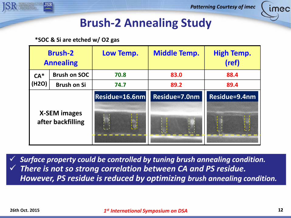
Brush-2 Annealing Study
26th Oct. 2015
Patterning Courtesy of imec
Brush-2Annealing
Low Temp. Middle Temp. High Temp.(ref)
CA*(H2O)
Brush on SOC 70.8 83.0 88.4
Brush on Si 74.7 89.2 89.4
X-SEM imagesafter backfilling
Residue=16.6nm Residue=9.4nm Residue=7.0nm
Surface property could be controlled by tuning brush annealing condition. There is not so strong correlation between CA and PS residue.
However, PS residue is reduced by optimizing brush annealing condition.
*SOC & Si are etched w/ O2 gas

1st International Symposium on DSA 1313
Contents
26th Oct. 2015
Introduction: DSA and Challenges for N7 and beyond
JSR materials development
• PS attractive brush for CH application
• BCP for LS application: PS-b-PMMA and High-chi BCP
Summary

1st International Symposium on DSA 1414
BCP for LS Application
26th Oct. 2015
YearLogic Node
Flash Pitch (HP)
L0=30.0nm
20232.5nm16(8)
20177nm
26(13)
201510nm30(15)
20195nm
22(11)
20213.5nm18(9)
PS-b-PMMA
Various research and application study
High-chi BCP
Well phase separationSub-20nm patterning
L0=24.2nm L0=20.9nm
L0=18.3nm L0=14.9nm
1st International Symposium on DSA 151526th Oct. 2015
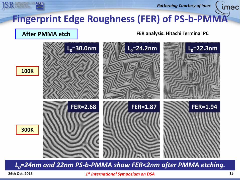
L0=22.3nmL0=24.2nmL0=30.0nm
FER=2.68 FER=1.87 FER=1.94
100K
300K
FER analysis: Hitachi Terminal PCAfter PMMA etch
L0=24nm and 22nm PS-b-PMMA show FER<2nm after PMMA etching.
Fingerprint Edge Roughness (FER) of PS-b-PMMA
Patterning Courtesy of imec

1st International Symposium on DSA 1616
JSR High-chi BCP
26th Oct. 2015
Organic OrganicWet removal unitc=0.09(vs PS)
<20nmP patterning Wet development ability
After Wet Dev.After Coat
Std.Wet Dev.
18.3nmP LS
Organic InorganicSi unit
c=0.12(vs PS) <20nmP patterning Higher etching selectivity
14.1nmP CH 14.9nmP LS 33.1nmP CH
100nm100nm100nm
For Sub-20nmP For >30nmPOrganic-Inorganic Type
Wet Removable Type

1st International Symposium on DSA 1717
Summary
26th Oct. 2015
• PS attractive brush for CH application
PS residue is reduced by processing PS attractive brush.
To achieve zero PS residue, PS attractive sidewall & neutral substrate should be required.
• BCP for LS application: PS-b-PMMA and High-chi BCP
L0=21nm lamellae PS-b-PMMA is synthesized.
Various type of high-chi BCP is continuously investigated.

1st International Symposium on DSA 1818
Acknowledgement
26th Oct. 2015
The authors gratefully thank to imec DSA team for various experimental
supports and useful discussion.
• Roel Gronheid
• Paulina Rincon Delgadillo
• Nadia Vandenbroeck
Thank you for your attention !!