discrete fourier transform v4 - xilinx · dft matlab mex function ... the xilinx® logicore™ ip...
TRANSCRIPT

Discrete Fourier Transform v4.0
LogiCORE IP Product Guide
Vivado Design Suite
PG106 November 18, 2015
Discrete Fourier Transform v4.0 www.xilinx.com 2PG106 November 18, 2015
Table of ContentsIP Facts
Chapter 1: OverviewFeature Summary. . . . . . . . . . . . . . . . . . . . . . . . . . . . . . . . . . . . . . . . . . . . . . . . . . . . . . . . . . . . . . . . . . 5Applications . . . . . . . . . . . . . . . . . . . . . . . . . . . . . . . . . . . . . . . . . . . . . . . . . . . . . . . . . . . . . . . . . . . . . . 5Licensing and Ordering Information . . . . . . . . . . . . . . . . . . . . . . . . . . . . . . . . . . . . . . . . . . . . . . . . . . . 5
Chapter 2: Product SpecificationPerformance. . . . . . . . . . . . . . . . . . . . . . . . . . . . . . . . . . . . . . . . . . . . . . . . . . . . . . . . . . . . . . . . . . . . . . 7Resource Utilization. . . . . . . . . . . . . . . . . . . . . . . . . . . . . . . . . . . . . . . . . . . . . . . . . . . . . . . . . . . . . . . . 8Port Descriptions . . . . . . . . . . . . . . . . . . . . . . . . . . . . . . . . . . . . . . . . . . . . . . . . . . . . . . . . . . . . . . . . . . 8
Chapter 3: Designing with the CoreClocking. . . . . . . . . . . . . . . . . . . . . . . . . . . . . . . . . . . . . . . . . . . . . . . . . . . . . . . . . . . . . . . . . . . . . . . . . . 9Resets . . . . . . . . . . . . . . . . . . . . . . . . . . . . . . . . . . . . . . . . . . . . . . . . . . . . . . . . . . . . . . . . . . . . . . . . . . . 9Protocol Description . . . . . . . . . . . . . . . . . . . . . . . . . . . . . . . . . . . . . . . . . . . . . . . . . . . . . . . . . . . . . . . 9Encoding of Size Parameter. . . . . . . . . . . . . . . . . . . . . . . . . . . . . . . . . . . . . . . . . . . . . . . . . . . . . . . . . 11
Chapter 4: Design Flow StepsCustomizing and Generating the Core . . . . . . . . . . . . . . . . . . . . . . . . . . . . . . . . . . . . . . . . . . . . . . . . 17Constraining the Core . . . . . . . . . . . . . . . . . . . . . . . . . . . . . . . . . . . . . . . . . . . . . . . . . . . . . . . . . . . . . 18Simulation . . . . . . . . . . . . . . . . . . . . . . . . . . . . . . . . . . . . . . . . . . . . . . . . . . . . . . . . . . . . . . . . . . . . . . 19Synthesis and Implementation . . . . . . . . . . . . . . . . . . . . . . . . . . . . . . . . . . . . . . . . . . . . . . . . . . . . . . 19
Chapter 5: C ModelFeatures . . . . . . . . . . . . . . . . . . . . . . . . . . . . . . . . . . . . . . . . . . . . . . . . . . . . . . . . . . . . . . . . . . . . . . . . 20Overview . . . . . . . . . . . . . . . . . . . . . . . . . . . . . . . . . . . . . . . . . . . . . . . . . . . . . . . . . . . . . . . . . . . . . . . 20Unpacking and Model Contents . . . . . . . . . . . . . . . . . . . . . . . . . . . . . . . . . . . . . . . . . . . . . . . . . . . . . 21Installation . . . . . . . . . . . . . . . . . . . . . . . . . . . . . . . . . . . . . . . . . . . . . . . . . . . . . . . . . . . . . . . . . . . . . . 21DFT C Model Interface . . . . . . . . . . . . . . . . . . . . . . . . . . . . . . . . . . . . . . . . . . . . . . . . . . . . . . . . . . . . . 21Compiling with the DFT C Model . . . . . . . . . . . . . . . . . . . . . . . . . . . . . . . . . . . . . . . . . . . . . . . . . . . . 24DFT MATLAB MEX Function. . . . . . . . . . . . . . . . . . . . . . . . . . . . . . . . . . . . . . . . . . . . . . . . . . . . . . . . . 25
Send Feedback

Discrete Fourier Transform v4.0 www.xilinx.com 3PG106 November 18, 2015
Appendix A: Migrating and UpgradingMigrating to the Vivado Design Suite. . . . . . . . . . . . . . . . . . . . . . . . . . . . . . . . . . . . . . . . . . . . . . . . . 26Upgrading in the Vivado Design Suite . . . . . . . . . . . . . . . . . . . . . . . . . . . . . . . . . . . . . . . . . . . . . . . . 26
Appendix B: DebuggingFinding Help on Xilinx.com . . . . . . . . . . . . . . . . . . . . . . . . . . . . . . . . . . . . . . . . . . . . . . . . . . . . . . . . . 27Debug Tools . . . . . . . . . . . . . . . . . . . . . . . . . . . . . . . . . . . . . . . . . . . . . . . . . . . . . . . . . . . . . . . . . . . . . 28Simulation Debug. . . . . . . . . . . . . . . . . . . . . . . . . . . . . . . . . . . . . . . . . . . . . . . . . . . . . . . . . . . . . . . . . 29
Appendix C: Additional Resources and Legal NoticesXilinx Resources . . . . . . . . . . . . . . . . . . . . . . . . . . . . . . . . . . . . . . . . . . . . . . . . . . . . . . . . . . . . . . . . . . 30References . . . . . . . . . . . . . . . . . . . . . . . . . . . . . . . . . . . . . . . . . . . . . . . . . . . . . . . . . . . . . . . . . . . . . . 30Revision History . . . . . . . . . . . . . . . . . . . . . . . . . . . . . . . . . . . . . . . . . . . . . . . . . . . . . . . . . . . . . . . . . . 31Please Read: Important Legal Notices . . . . . . . . . . . . . . . . . . . . . . . . . . . . . . . . . . . . . . . . . . . . . . . . 31
Send Feedback
Discrete Fourier Transform v4.0 www.xilinx.com 4PG106 November 18, 2015 Product Specification
IntroductionThe Xilinx® LogiCORE ™ IP Discrete Fourier Transform (DFT) core meets the requirements for 3GPP Long Term Evolution (LTE) [Ref 1] systems.
The point size of the transformation (N) can be specif ied on a frame-by-frame basis and can take the values N=2M*3P*5Q, where M, P, and Q can be set to a range of values (as in Table 3-1) that meet the LTE system requirements.
Features• Support for wide range of transform sizes,
including 1296 and 1536
• Less than 26 μs total latency when transforming 1200 points at 245.76 MHz (using any combination of sizes)
• Size can be changed for each transform
• Up to 18-bit twos complement input data width, up to 18-bit twos complement output data width with 4-bit block exponent
• Direct and inverse DFT supported on frame-by-frame basis
IP Facts
LogiCORE IP Facts Table
Core Specifics
Supported Device Family(1)
UltraScale+™ FamiliesUltraScale™ Architecture
Zynq®-7000 All Programmable SoC7 Series
Supported User Interfaces N/A
Resources Performance and Resource Utilization web page
Provided with CoreDesign Files Encrypted RTL
Example Design Not Provided
Test Bench Not Provided
Constraints File Not Provided
Simulation Model
VHDL BehavioralVHDL or Verilog Structural
C Model
Supported S/W Driver N/A
Tested Design Flows(2)
Design Entry Vivado® Design Suite
Simulation For supported simulators, see theXilinx Design Tools: Release Notes Guide.
Synthesis Vivado Synthesis
SupportProvided by Xilinx at the Xilinx Support web page
Notes: 1. For a complete listing of supported devices, see the Vivado IP
catalog. 2. For the supported versions of the tools, see the
Xilinx Design Tools: Release Notes Guide.
Send Feedback
Discrete Fourier Transform v4.0 www.xilinx.com 5PG106 November 18, 2015
Chapter 1
OverviewThe Discrete Fourier Transform IP core implements forward and inverse DFTs for a wide range of user-selectable point sizes. The point size and transform direction may be changed on a per-frame basis. The core supports input data widths of 8 to 18 bits, in twos complement format.
Feature SummaryThe Discrete Fourier Transform core supports a wide range of point sizes, including 1296 and 1536 for the 3GPP LTE standard. The point size and the transform direction may be changed on a frame-by-frame basis.
A bit-accurate C model is delivered with the core to support software simulation.
ApplicationsThe Discrete Fourier Transform core may be used to perform a forward or inverse Fourier transform on data frames which are not a power of two in size.
The supported point sizes cover the requirements of the 3GPP LTE standard for a DFT in the baseband uplink. The core may also be used for general DFT applications such as spectral analysis or convolution in the frequency domain.
Licensing and Ordering InformationThis Xilinx® LogiCORE™ IP module is provided at no additional cost with the Xilinx Vivado® Design Suite under the terms of the Xilinx End User License. Information about this and other Xilinx LogiCORE IP modules is available at the Xilinx Intellectual Property page. For information about pricing and availability of other Xilinx LogiCORE IP modules and tools, contact your local Xilinx sales representative.
Send Feedback

Discrete Fourier Transform v4.0 www.xilinx.com 6PG106 November 18, 2015
Chapter 2
Product SpecificationThe forward DFT output is related to the input by the following equation:
where and the input, , is a complex quantity in which and are twos complement f ixed-point numbers whose values are given by:
where is the t-th bit of .
The output is a complex block floating-point quantity whose value is given by:
where and are twos complement numbers as defined previously, and the block exponent, , is an unsigned integer with weighted binary representation:
where is the t-th bit of . The block exponent is constant for all elements of a particular DFT output frame.
The inverse DFT has the following relationship between input and output:
X k( ) x n( )e
j2πnk–N
---------------
n 0=
N 1–
= k 0 … N 1–, ,=
j 1–= x n( ) xr n( ) jxi n( )+ xr n( )xi n( )
x x17– xt217– t+
t 0=
16
+=
xt x
X k( )
Xr k( ) jXi k( )+( )2b
Xr k( ) Xi k( )b
b bt2t
t 0=
3
=
bt b
x n( ) X k( )e
j2πnkN
-------------
k 0=
N 1–
= n 0 … N 1–, ,=
Send Feedback
Discrete Fourier Transform v4.0 www.xilinx.com 7PG106 November 18, 2015
Chapter 2: Product Specification
Again, the input is represented as a complex twos complement f ixed-point value, and the output a complex block floating-point value, as defined for the forward transform.
Note that neither the forward nor inverse DFT provides scaling by 1/N.
Format of Input/Output DataFor all bit widths, the f ixed point is to the right of the MSB, that is, such that data 'x' takes the range -1.0 ≤ x <1.0. For best numerical performance twos complement input data, that is, less than 18-bits should be zero padded in the least significant bit positions.
Block exponent (BLK_EXP) is the power of 2 in the block floating point representation for the output data. Its range is from 0 to 15.
Performance
DFT ThroughputThe throughput of the design, measured in terms of the number of DFTs per cycle, is given by 1/CT where CT is the total number of cycles between frames of input data. The value of CT for each transform size is summarized in Table 3-1.
DFT Latency
Single Transform Latency
The minimum latency of the core is defined as the number of cycles from first input to last output. It is summarized in Table 3-1.
Multiple Transform Latency
The minimum latency for multiple transforms is obtained by adding the values of CT for each size, and CL for the last transform. The latency for V transforms of the same size is given by the following equation:
The time to process 1200 points, as summarized in Table 3-1 and Table 3-2, has been derived from the preceding equation and the clock period. Note that for point sizes larger than 600, V is given by 1200/N, where N is the point size. The choice of 1200 point as the size is driven by the fact that 1200 point array seems to be the most typical case in the LTE systems.
Total Latency V 1–( )CT CL+=
Send Feedback

Discrete Fourier Transform v4.0 www.xilinx.com 8PG106 November 18, 2015
Chapter 2: Product Specification
Resource UtilizationFor full details about performance and resource utilization, visit the Performance and Resource Utilization web page.
Port DescriptionsThe pin-out of the DFT is summarized in Table 2-1.
Table 2-1: Pinout
Name Width Direction Description
XN_RE N(1) INPUT Real Data Input: Provide in twos complement f ixed-point format. Provide in natural order.
XN_IM N(1) INPUT Imaginary Data Input: Provide in twos complement f ixed-point format. Provide in natural order.
FD_IN 1 INPUT First Data In: Set High to indicate start of data input frame. FD_IN is ignored when RFFD is Low.
RFFD 1 OUTPUT Ready For First Data: High when the core is ready for a new frame of data. Goes Low one cycle after a valid FD_IN.
SIZE 6 INPUT Size In: Size of transform to be performed. Sampled when FD_IN is High (that is, at start of data frame).
FWD_INV 1 INPUTTransform Direction: Set High to perform forward transform or Low for inverse transform. Sampled when FD_IN is High (that is, at start of data frame).
SCLR 1 INPUT
Synchronous Clear: Set High for a single cycle to reset the core. This must be performed after power-on. If the core is processing data at the time a reset is performed, then processing is halted immediately and any intermediate data is discarded. After reset the core is ready to accept new input frames.
CLK 1 INPUT Clock
CE 1 INPUT Clock Enable: Clock enable has lower precedence than SCLR
XK_RE N(1) OUTPUT Real Data Output: Provided in natural order and in f ixed-point format.
XK_IM N(1) OUTPUT Imaginary Data Output: Provided in natural order and in f ixed-point format.
BLK_EXP 4 OUTPUT Block exponent: Provided as unsigned integer.
FD_OUT 1 OUTPUT First Data Out: Set High by core to indicate that the core is ready to output data.
DATA_VALID 1 OUTPUT Data Valid: Set High by core to indicate that data output is valid.
Notes: 1. N is number of bits per single value, real or imaginary.
Send Feedback
Discrete Fourier Transform v4.0 www.xilinx.com 9PG106 November 18, 2015
Chapter 3
Designing with the CoreThis chapter includes guidelines and additional information to facilitate designing with the core.
ClockingThe core requires a single clock, CLK, and is active-High triggered. If selected, the active-High clock enable, CE, stalls all core processing when de-asserted.
ResetsThe DFT has a single active-High synchronous reset, SCLR. Asserting SCLR for a single cycle resets the core. SCLR overrides CE if both controls are present on the core.
Protocol DescriptionThe DFT design has a fully synchronous interface. Figure 3-1 shows the pinout of the design. See Table 2-1 for more details on ports.
Send Feedback
Discrete Fourier Transform v4.0 www.xilinx.com 10PG106 November 18, 2015
Chapter 3: Designing with the Core
The core indicates that it is ready to accept a new frame of data by setting RFFD High. When RFFD is High, data input may be started by setting FD_IN High for one or more cycles. Data is input via XN_RE and XN_IM. It should be provided over N cycles without interruption. Data input and output are complex and in natural order. FD_OUT signals when the core starts data output and DATA_VALID signals when data on XK_RE and XK_IM is valid.
Note that FD_IN is ignored while RFFD is Low, and so FD_IN can be kept High for multiple cycles. FD_IN is accepted on the f irst cycle that RFFD is High.
If FD_IN is set permanently High, then the core will start a new frame of data input as soon as the core is ready. This arrangement provides maximum transform throughput. Alternatively, RFFD may be connected directly to FD_IN to achieve the same behavior.
The f irst element of input data should be provided on the same cycle that the core starts to receive data, that is, the first cycle in which both FD_IN and RFFD are High.
Input and Output TimingFigure 3-2 provides a timing diagram for the DFT input and output. It shows a forward transform being followed by an inverse transform.
Data input and output is partially overlapped with processing to minimize the latency, CL, of the core. Initially, input data is copied into the intermediate buffer. Once 3N/4 elements have been written to the buffer, the DFT starts performing the f irst layer of radix-4 operations (denoted R4 in Figure 3-2). Subsequent input data is fed directly into the DFT as each radix-4 operation is performed.
Similarly, data output is overlapped with the last layer of radix-3 operations (denoted R3 in Figure 3-2), with the first N/3 samples coming directly from the radix-r unit. The remaining
X-Ref Target - Figure 3-1
Figure 3-1: Interface Diagram
Send Feedback
Discrete Fourier Transform v4.0 www.xilinx.com 11PG106 November 18, 2015
Chapter 3: Designing with the Core
outputs of the radix-r unit are temporarily stored in the intermediate buffer and output over the next 2N/3 cycles.
Encoding of Size ParameterThe transform size, N, should be selected via the SIZE input using the binary encoding presented in Table 3-1. For each transform size, the table also indicates the latency of the design, CL, and minimum cycles between input frames, CT. The latency is defined here as the number of cycles between the f irst element of input data and last element of output data.
Also shown in Table 3-1 is the total time to operate on 1200 points using N-point transforms. For example, when N=12 this is the time to perform 100 12-point transforms
Additional size 1536 can be selected only if the core synthesized with the “Support size 1536” parameter on. Then the core requires one extra block RAM to store the additional coeff icients and will run slightly slower.
X-Ref Target - Figure 3-2
Figure 3-2: Interface Timing Diagram
Table 3-1: Support for DFT Transform Size
Size(Binary) N M
(Radix-2)P
(Radix-3)Q
(Radix-5)Latency CL
CyclesPeriod CT
CyclesTime to Process 1200 Points,
s (at 245.76 MHz)
0 12 2 1 75 62 25.28
1 24 3 1 122 109 22.22
μ
Send Feedback

Discrete Fourier Transform v4.0 www.xilinx.com 12PG106 November 18, 2015
Chapter 3: Designing with the Core
2 36 2 2 152 139 18.90
3 48 4 1 176 163 16.63
4 60 2 1 1 227 214 17.46
5 72 3 2 271 258 17.55
6 96 5 1 325 312 15.92
7 108 2 3 373 360 16.32
8 120 3 1 1 418 405 16.53
9 144 4 2 457 444 15.10
10 180 2 2 1 592 579 15.76
11 192 6 1 565 552 14.09
12 216 3 3 732 719 16.30
13 240 4 1 1 736 723 14.76
14 288 5 2 918 905 15.39
15 300 2 1 2 955 942 15.38
16 324 2 4 1074 1061 16.04
17 360 3 2 1 1191 1178 16.03
18 384 7 1 1158 1145 14.61
19 432 4 3 1362 1349 15.30
20 480 5 1 1 1509 1496 15.27
21 540 2 3 1 1773 1760 15.96
22 576 6 2 1734 1721 14.64
23 600 3 1 2 1962 1949 15.91
24 648 3 4 2225 2212 16.72
25 720 4 2 1 2265 2252 15.32
26 768 8 1 2214 2201 14.04
27 864 5 3 2855 2842 16.11
28 900 2 2 2 2952 2939 15.99
29 960 6 1 1 2901 2888 14.74
30 972 2 5 3359 3346 16.86
31 1080 3 3 1 3716 3703 16.79
32 1152 7 2 3671 3658 15.55
33 1200 4 1 2 3792 3779 15.43
34 1296 4 4 0 4331 4318 17.63(1)
35 1536 9 1 0 4727 4714 19.24(1)
Notes: 1. These times are given for the full transform rather than for 1200 point size.
Table 3-1: Support for DFT Transform Size (Cont’d)
Size(Binary) N M
(Radix-2)P
(Radix-3)Q
(Radix-5)Latency CL
CyclesPeriod CT
CyclesTime to Process 1200 Points,
s (at 245.76 MHz)μ
Send Feedback
Discrete Fourier Transform v4.0 www.xilinx.com 13PG106 November 18, 2015
Chapter 3: Designing with the Core
DFT OperationThe N-point DFT is decomposed into relatively prime factors: 2M, 3P and 5Q, where the total transform size is given by N=2M*3P*5Q. This is shown diagrammatically in Figure 3-3.
Each prime factor is implemented by breaking it down into the appropriate number of common factors. These are implemented using radix-2, -3, -4 and -5 butterfly operations as shown in Figure 3-4. Note that the 2M prime factor has been implemented using a combination of radix-2 and radix-4 butterflies. The multiplications required between common factors are not shown, and are implemented within the butterfly, on its input.
The radix-2, -3, -4, and -5 operations are performed using a single pipelined, parallel radix-r unit. This is capable of performing two radix-2 operations per clock cycle, one radix-3 or radix-4 operation per cycle and one radix-5 operation per two clock cycles as shown in Figure 3-5.
X-Ref Target - Figure 3-3
Figure 3-3: Factorization of DFT
X-Ref Target - Figure 3-4
Figure 3-4: Full Factorization of DFT
X-Ref Target - Figure 3-5
Figure 3-5: Radix-r Unit
2M
N/2M
2M
5Q 3P
5Q
N/5Q N/3P
3P
Inputs Output
R4
R4
R2 R3 R3R5
N/4
R4 R5
N/2
R2 R3 R3R5R4 R5
N/3 N/5Inputs Output
M/2-layers P-layers Q-layers
R4 Stages included if required by transform size
Radix-rR4
R3
R2R2
R5cycle-1
cycle-2
RADIX
RADIX=3
RADIX=4
RADIX=2
RADIX=5
Send Feedback

Discrete Fourier Transform v4.0 www.xilinx.com 14PG106 November 18, 2015
Chapter 3: Designing with the Core
Radix-r Unit
Figure 3-6 and Figure 3-7 show the radix-3 and radix-5 butterfly operations used by the DFT. They include the twiddle factor multiplications on the input required to cascade factors to obtain a 2M*3P*5Q point DFT. The diagrams also show the internal word lengths adopted, and include the scaling and rounding blocks required to implement block-floating-point. Their function is explained in the next section.
The radix-5 butterfly is performed using two passes of the radix-r unit. The first pass performs the twiddle-factor multiplications and first two stages of adders. At this point, scaling and rounding are applied to reduce word length to that of the input, so that it may be fed back for the second pass. The worst-case word growth for the first half is equivalent to that of the whole butterfly, so no further scaling is applied in the second pass. The second pass performs the intermediate multiplies and the f inal two stages of addition. Quantization reduces the word length to that of the input, so that it may be stored in the intermediate memory, ready for the next stage.
X-Ref Target - Figure 3-6
Figure 3-6: Radix-3 Winograd Butterfly
j0.866 (0x1BB68)
TW 1 0.5
r s t
t r s
max
TW 2
2.20-bits
1.17-bits
x(0)
x(1)
x(2)
scale_calc
X(1)
X(2)
3.20-b its1.17-bits
t
t
t
4.20-bits 4.20-b its 1.17-b its
margin_in
exp_in exp_out
margin_out
X(0)r s
3.20-bits
4.20-bits
4.20-bits
1.17-bits
1.17-b its
2.34-bits
4.37-bits
t Truncation
r Round (to nearest) w ith saturation
4-bits (msbs)
2-bits
4-bits
1.17-bits
1.17-bits
1.17-bits
s Shif t right by 1-b it
3.20-bits2.34-bits 2.20-b its
4.20-bits 4.20-bits
4.20-bits
1.17-bits
4.20-b its Two’s complement fixed-point number with 20 fract ional
Key
4.23-bits
4.23-bits
4.23-bits
s
3.21-bits
s Shif t
0.5
Send Feedback

Discrete Fourier Transform v4.0 www.xilinx.com 15PG106 November 18, 2015
Chapter 3: Designing with the Core
Block Floating-Point Behavior
Word length growth within the transform is accommodated by block floating-point. This is achieved by scaling the output of the radix-r unit by a power of 2 to keep a data word length of 18-bits. To reduce implementation cost, the level of scaling is either 0, 1, 2 or 3-bit shift, allowing its implementation using a 4-1 multiplexer.
The level of scaling is calculated by establishing the maximum size of the layer input, and the maximum word growth possible through the layer.
This growth is bits per radix-r layer. The scaling occurs when a complex input with full-scale positive or negative real or imaginary parts, is rotated by 45 degrees. Rotations are required between layers as a result of the factorization of the DFT algorithm. The f irst layer requires no twiddle-factors, and so the word growth is exactly 2 bits and the associated scaling is 1/4, which is obtained by a 2-bit right-shift. The worst-case scaling applied for each radix is summarized in Table 3-2.
X-Ref Target - Figure 3-7
Figure 3-7: Radix-5 Winograd Butterfly
j0.951 (0x2E6F1)
-j0.362 (0x34601)
-j1.539 (0x6EC1D)
0.559 (0x11E37)
TW1 0.25
r s t
t
t
t
r s
r s
r s
max
TW2
TW3
TW4
2.20-bits
1.17-bits
x(0)
x(1)
x(2)
x(3)
x(4)
s
s
s
s
r
r
r
r
max
scale_calc
scale_calc
s r
X(0)
X(4)
X(2)
X(3)
X(1)
3.20-bits 4.20-bits
t
t
t
3.20-bits 4.20-bits
t
margin_in
exp_in exp_out
margin_out
r s
4-bits (msbs)
4-bits
2-bits
2.34-bits
s
2.17-bits
s
1.17-bits
t
4.20-bits
4.20-bits
4.20-bits
4.23-bits
Intermediate twiddle factors shown for forward transform
4.23-bits
4.23-bits
4.23-bits
4.23-bits
1.17-bits
1.17-bits
1.17-bits
1.17-bits
2.34-bits
2.34-bits
2.34-bits
2.20-bits
2.20-bits
2.20-bits
3.20-bits
3.20-bits
3.20-bits
4.20-bits
4.20-bits
4.23-bits
3.23-bits
3.23-bits
4.23-bits
4.23-bits
2.19-bits
2.34-bits
2.34-bits
2.34-bits
2.20-bits
2.20-bits
2.20-bits
2.20-bits2.34-bits
1.17-bits
1.17-bits
1.17-bits 1.17-bits
1.17-bits
1.17-bits
1.17-bits
3.20-bits
3.20-bits
3.20-bits
2.20-bits 1.17-bits
1.17-bits
1.17-bits
1.17-bits
1.17-bits
1.17-bits
1.17-bits
1.17-bits
1.17-bits
1.17-bits
1.17-bits
Table 3-2: Power-of-2 Scaling Required to Accommodate Worst-Case Growth
Radix-4 Layer Worst-Case Growth Power-2 Scaling
Radix-2 2.414 4
Radix-3 3.828 4
Radix-4 First layer 2.000 2
Radix-4 Other layer 5.243 8
Radix-5 6.657 8
log2 1 r 1–( ) 2+( ) 2
Send Feedback
Discrete Fourier Transform v4.0 www.xilinx.com 16PG106 November 18, 2015
Chapter 3: Designing with the Core
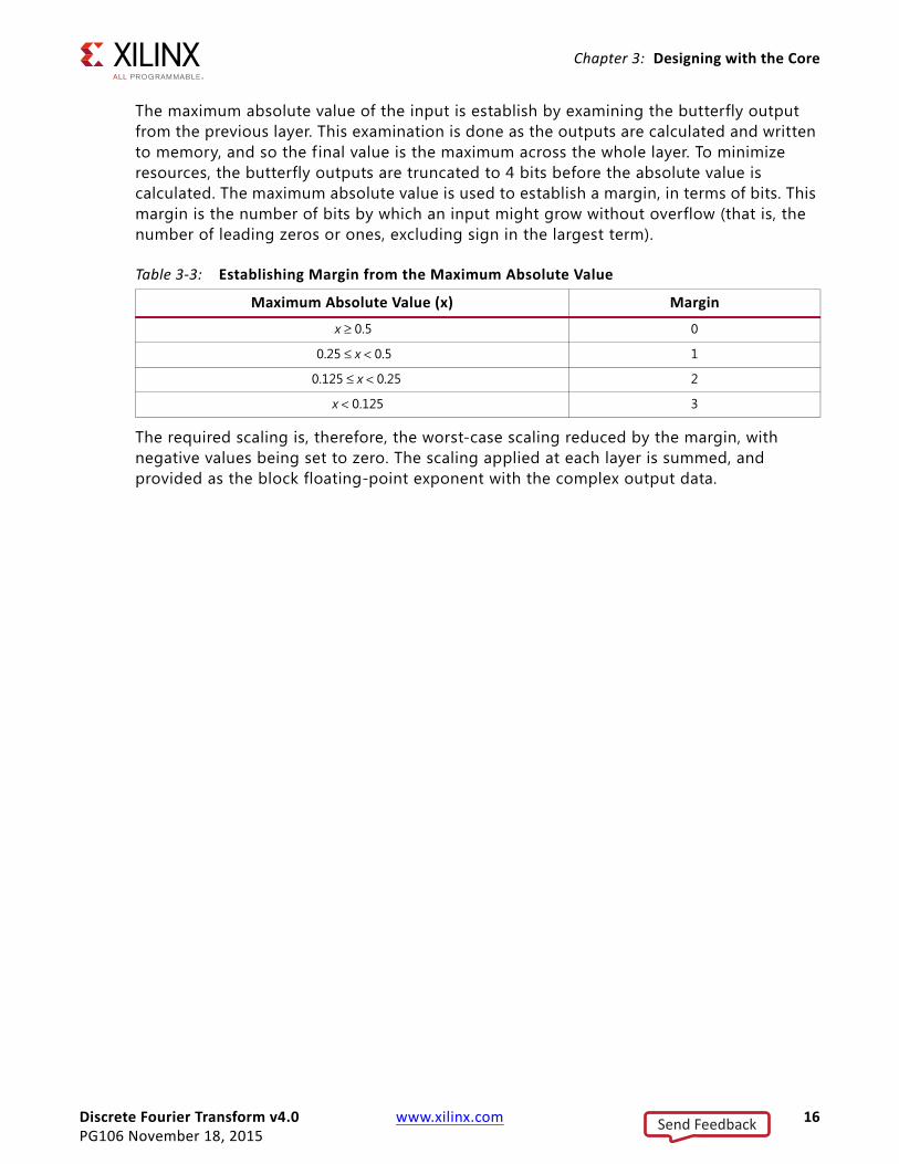
The maximum absolute value of the input is establish by examining the butterfly output from the previous layer. This examination is done as the outputs are calculated and written to memory, and so the final value is the maximum across the whole layer. To minimize resources, the butterfly outputs are truncated to 4 bits before the absolute value is calculated. The maximum absolute value is used to establish a margin, in terms of bits. This margin is the number of bits by which an input might grow without overflow (that is, the number of leading zeros or ones, excluding sign in the largest term).
The required scaling is, therefore, the worst-case scaling reduced by the margin, with negative values being set to zero. The scaling applied at each layer is summed, and provided as the block floating-point exponent with the complex output data.
Table 3-3: Establishing Margin from the Maximum Absolute Value
Maximum Absolute Value (x) Margin
0
1
2
3
x 0.5≥
0.25 x 0.5<≤
0.125 x 0.25<≤
x 0.125<
Send Feedback

Discrete Fourier Transform v4.0 www.xilinx.com 17PG106 November 18, 2015
Chapter 4
Design Flow StepsThis chapter describes customizing and generating the core, constraining the core, and the simulation, synthesis and implementation steps that are specific to this IP core. More detailed information about the standard Vivado® design flows and the IP integrator can be found in the following Vivado Design Suite user guides:
• Vivado Design Suite User Guide: Designing IP Subsystems using IP Integrator (UG994) [Ref 2]
• Vivado Design Suite User Guide: Designing with IP (UG896) [Ref 3]
• Vivado Design Suite User Guide: Getting Started (UG910) [Ref 4]
• Vivado Design Suite User Guide: Logic Simulation (UG900) [Ref 5]
Customizing and Generating the CoreThis section includes information about using Xilinx tools to customize and generate the core in the Vivado Design Suite.
If you are customizing and generating the core in the Vivado IP Integrator, see the Vivado Design Suite User Guide: Designing IP Subsystems using IP Integrator (UG994) [Ref 2] for detailed information. IP Integrator might auto-compute certain configuration values when validating or generating the design. To check whether the values do change, see the description of the parameter in this chapter. To view the parameter value you can run the validate_bd_design command in the Tcl console.
Vivado Integrated Design EnvironmentYou can customize the IP for use in your design by specifying values for the various parameters associated with the IP core using the following steps:
1. Select the IP from the IP catalog.
2. Double-click the selected IP or select the Customize IP command from the toolbar or right-click menu.
For details, see the Vivado Design Suite User Guide: Designing with IP (UG896) [Ref 3] and the Vivado Design Suite User Guide: Getting Started (UG910) [Ref 4].
Send Feedback

Discrete Fourier Transform v4.0 www.xilinx.com 18PG106 November 18, 2015
Chapter 4: Design Flow Steps
The DFT core GUI has a single page with f ields to set parameter values for the particular instantiation required. This section provides a description of each f ield.
Component Name: The name of the core component to be instantiated. the name must begin with a letter and be composed of the following characters: a to z, 0 to 9, and "_".
Precision Options: Selects the input and output data width required.
Optimization: Selects whether the core should be optimized for resources or performance.
Optional Pins:
• CE: Selects if the core has a clock enable control pin.
• SCLR: selects if the core has a synchronous reset control pin.
Enable 1536 point size support: Enables support for the 1536-point transform for 3GPP LTE systems. Selecting this option requires additional hardware resources.
User ParametersTable 4-1 shows the relationship between the GUI f ields in the Vivado IDE (described in Vivado Integrated Design Environment) and the User Parameters (which can be viewed in the Tcl console).
Output GenerationFor details, see the Vivado Design Suite User Guide: Designing with IP (UG896) [Ref 3].
Constraining the CoreThis section contains information about constraining the core in the Vivado Design Suite.
Required ConstraintsThis section is not applicable for this IP core.
Table 4-1: GUI Parameter to User Parameter Relationship
GUI Parameter User Parameter Default Value
Input/Output Data Width data_width 18
Optimization speed_optimization Area
CE clock_enable False
SCLR synchronous_clear True
Enable 1536 point size support support_size_1536 false
Send Feedback
Discrete Fourier Transform v4.0 www.xilinx.com 19PG106 November 18, 2015
Chapter 4: Design Flow Steps
Device, Package, and Speed Grade SelectionsThis section is not applicable for this IP core.
Clock FrequenciesThis section is not applicable for this IP core.
Clock ManagementThis section is not applicable for this IP core.
Clock PlacementThis section is not applicable for this IP core.
BankingThis section is not applicable for this IP core.
Transceiver PlacementThis section is not applicable for this IP core.
I/O Standard and PlacementThis section is not applicable for this IP core.
SimulationFor comprehensive information about Vivado simulation components, as well as information about using supported third party tools, see the Vivado Design Suite User Guide: Logic Simulation (UG900) [Ref 5].
Synthesis and ImplementationFor details about synthesis and implementation, see the Vivado Design Suite User Guide: Designing with IP (UG896) [Ref 3].
Send Feedback

Discrete Fourier Transform v4.0 www.xilinx.com 20PG106 November 18, 2015
Chapter 5
C ModelThe Xilinx® LogiCORE™ IP Discrete Fourier Transform (DFT) core has a bit accurate C model designed for system modeling. An example MATLAB ® MEX function for MATLAB integration is also available. The C model is produced when the core is generated in the Vivado® Design Suite.
Features• Bit accurate to DFT core
• Available for 32-bit and 64-bit Linux platforms
• Available for 32-bit and 64-bit Windows platforms
• Supports all features of the DFT that affect numerical results
• Designed for integration into a larger system model
• Example of C++ code provided showing how to use the function
• MATLAB MEX function with an example script for Windows
OverviewThe DFT bit accurate C model has an interface consisting of a set of C functions that reside in a dynamic link library (shared library). Full details of the interface are given in DFT C Model Interface and an example piece of C++ code showing how to call the model is provided.
The model is also available as a MATLAB MEX function for MATLAB integration. The model is bit accurate but not cycle-accurate, so it produces exactly the same output data as the core on a frame-by-frame basis. However, it does not model the core latency or its interface signals.
Send Feedback

Discrete Fourier Transform v4.0 www.xilinx.com 21PG106 November 18, 2015
Chapter 5: C Model
Unpacking and Model ContentsUnzipping the DFT C model ZIP f ile produces the files shown in Table 5-1 and Table 5-2.
InstallationOn Linux, ensure that the directory in which the file libIp_dft_v4_0_bitacc_cmodel.so is located is on your $LD_LIBRARY_PATH environment variable.
On Windows, ensure that the directory in which the file libIp_dft_v4_0_bitacc_cmodel.dll is located is either on your $PATH environment variable, or is the directory in which you run your executable that calls the DFT C model.
DFT C Model InterfaceNote: An example C++ file, run_bitacc_cmodel.c is included that demonstrates how to call the DFT C model. See this f ile for examples of using the interface described in this chapter.
The C model is used through three functions declared in the header f ile, dft_v4_0_bitacc_cmodel.h:
Table 5-1: C Model ZIP File Contents for Linux
File Descriptiondft_v4_0_bitacc_cmodel.h Header file which defines the model API
libIp_dft_v4_0_bitacc_cmodel.so Model shared object library
run_bitacc_cmodel.cpp Example code calling the C model
dft_v4_0_bitacc_mex.cpp MATLAB® MEX function source
make_dft_v4_0_mex.m MEX function compilation script
run_dft_v4_0_mex.m MATLAB example script to run the MEX function
Table 5-2: C Model ZIP File Contents for Windows
File Descriptiondft_v4_0_bitacc_cmodel.h Header file which defines the model API
libIp_dft_v4_0_bitacc_cmodel.dll Model dynamically linked library
libIp_dft_v4_0_bitacc_cmodel.lib Model object .lib file for compiling and linking
run_bitacc_cmodel.cpp Example code calling the C model
dft_v4_0_bitacc_mex.cpp MATLAB MEX function source
make_dft_v4_0_mex.m MEX function compilation script
run_dft_v4_0_mex.m MATLAB example script to run the MEX function
Send Feedback
Discrete Fourier Transform v4.0 www.xilinx.com 22PG106 November 18, 2015
Chapter 5: C Model
struct xilinx_ip_dft_v4_0_state* xilinx_ip_dft_v4_0_create_state(struct xilinx_ip_dft_v4_0_generics generics
);
int xilinx_ip_dft_v4_0_bitacc_simulate(struct xilinx_ip_dft_v4_0_state* state,struct xilinx_ip_dft_v4_0_inputs inputs,struct xilinx_ip_dft_v4_0_outputs* outputs
);
void xilinx_ip_dft_v4_0_destroy_state(struct xilinx_ip_dft_v4_0_state* state
);
1. To use the model, f irst create a state structure using the f irst function, xilinx_ip_dft_v4_0_create_state.
2. Then run the model using the second function, xilinx_ip_dft_v4_0_bitacc_simulate, passing the state structure, an inputs structure, and an outputs structure to the function.
3. Finally, free up memory allocated for the state structure using the third function, xilinx_ip_dft_v4_0_destroy_state. Each of these functions is described fully below.
Create a State StructureThe f irst function, xilinx_ip_dft_v4_0_create_state, creates a new state structure for the DFT C model, allocating memory to store the state as required, and returns a pointer to that state structure. The state structure contains all the information required to define the DFT being modelled. The function is called with a structure containing the core's generics. The generics are all of the parameters that define the bit accurate numerical performance of the core. In the current version, the user should set up only one f ield in xilinx_ip_dft_v4_0_generics: C_DATA_WIDTH. It specif ies the input/output and internal precision of the data in bits; the permitted range of C_DATA_WIDTH is 8 to 18 and its default value is 18. The xilinx_ip_dft_v4_0_create_state function fails with an error message and returns a NULL pointer if a generic is invalid.
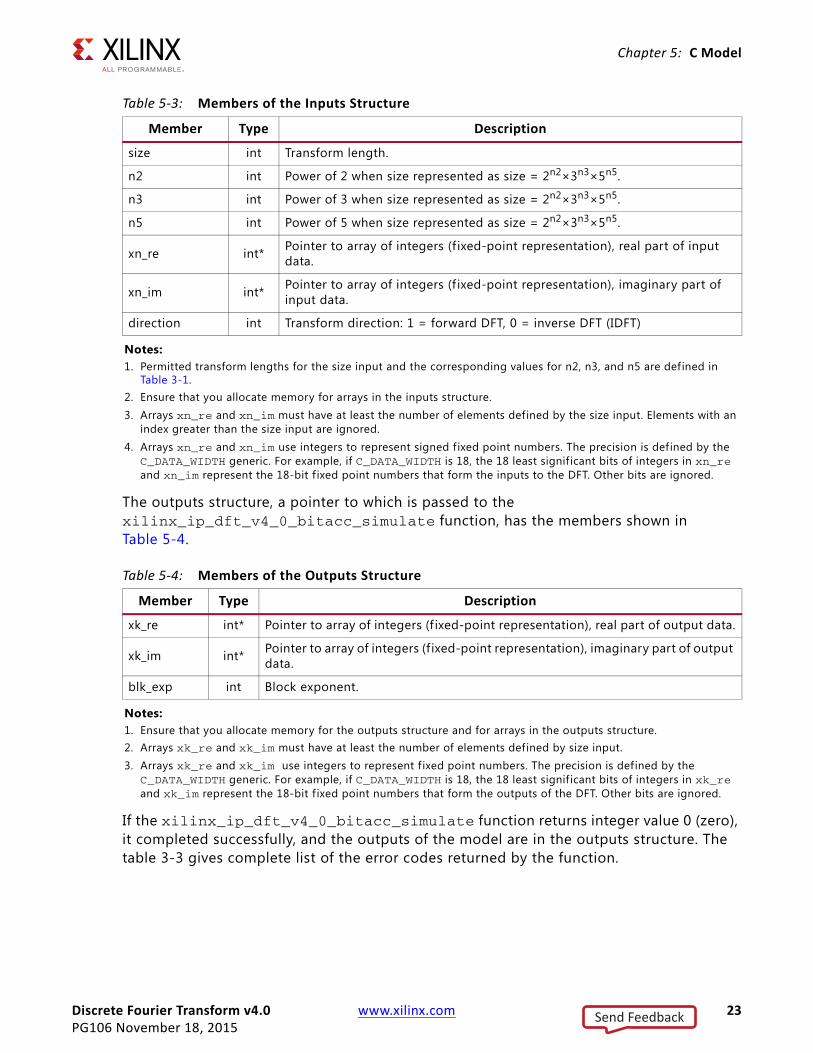
Simulate the DFT CoreAfter a state structure has been created, it can be used as many times as required to simulate the DFT core. A simulation is run using the second function, xilinx_ip_dft_v4_0_bitacc_simulate. Call this function with the pointer to the existing state structure and structures that hold the inputs and outputs of the C model. The inputs structure members are shown in Table 5-3.
Send Feedback
Discrete Fourier Transform v4.0 www.xilinx.com 23PG106 November 18, 2015
Chapter 5: C Model
.
The outputs structure, a pointer to which is passed to the xilinx_ip_dft_v4_0_bitacc_simulate function, has the members shown in Table 5-4.
If the xilinx_ip_dft_v4_0_bitacc_simulate function returns integer value 0 (zero), it completed successfully, and the outputs of the model are in the outputs structure. The table 3-3 gives complete list of the error codes returned by the function.
Table 5-3: Members of the Inputs Structure
Member Type Description
size int Transform length.
n2 int Power of 2 when size represented as size = 2n2×3n3×5n5.
n3 int Power of 3 when size represented as size = 2n2×3n3×5n5.
n5 int Power of 5 when size represented as size = 2n2×3n3×5n5.
xn_re int* Pointer to array of integers (f ixed-point representation), real part of input data.
xn_im int* Pointer to array of integers (f ixed-point representation), imaginary part of input data.
direction int Transform direction: 1 = forward DFT, 0 = inverse DFT (IDFT)
Notes: 1. Permitted transform lengths for the size input and the corresponding values for n2, n3, and n5 are defined in
Table 3-1.2. Ensure that you allocate memory for arrays in the inputs structure.3. Arrays xn_re and xn_im must have at least the number of elements defined by the size input. Elements with an
index greater than the size input are ignored.4. Arrays xn_re and xn_im use integers to represent signed f ixed point numbers. The precision is defined by the
C_DATA_WIDTH generic. For example, if C_DATA_WIDTH is 18, the 18 least signif icant bits of integers in xn_re and xn_im represent the 18-bit f ixed point numbers that form the inputs to the DFT. Other bits are ignored.
Table 5-4: Members of the Outputs Structure
Member Type Description
xk_re int* Pointer to array of integers (f ixed-point representation), real part of output data.
xk_im int* Pointer to array of integers (f ixed-point representation), imaginary part of output data.
blk_exp int Block exponent.
Notes: 1. Ensure that you allocate memory for the outputs structure and for arrays in the outputs structure.2. Arrays xk_re and xk_im must have at least the number of elements defined by size input.3. Arrays xk_re and xk_im use integers to represent f ixed point numbers. The precision is defined by the
C_DATA_WIDTH generic. For example, if C_DATA_WIDTH is 18, the 18 least signif icant bits of integers in xk_re and xk_im represent the 18-bit f ixed point numbers that form the outputs of the DFT. Other bits are ignored.
Send Feedback
Discrete Fourier Transform v4.0 www.xilinx.com 24PG106 November 18, 2015
Chapter 5: C Model
Destroy the State StructureFinally, the state structure must be destroyed to free up memory used to store the state, using the third function, xilinx_ip_dft_v4_0_destroy_state, called with the pointer to the existing state structure.
If the generics of the core need to be changed, destroy the existing state structure and create a new state structure using the new generics.
Compiling with the DFT C ModelPlace the header f ile, dft_v4_0_bitacc_cmodel.h, with your other header f iles. Compilation varies from platform to platform.
Linux (32-bit and 64-bit)Reference the shared library file used by the model, libIp_dft_v4_0_bitacc_cmodel.so.
Using GCC, linking is typically achieved by adding the following command line options: -L.-lIp_dft_v4_0_bitacc_cmodel
Note: This assumes that the shared object libraries are in the current directory. If this is not the case, the -L. option should be changed to specify the library search path to use.
On Linux, ensure that the directory in which the file, libIp_dft_v4_0_bitacc_cmodel.so is located is on your $LD_LIBRARY_PATH environment variable.
Here is an example GCC command line:
gcc -x c++ run_bitacc_cmodel.cpp -o run_bitacc_cmodel -L. -lIp_dft_v4_0_bitacc_cmodel
The specif ic syntax can differ depending on the user settings, and because the library was compiled with GNU C++ compiler v4.1.1, the compiler has to be compatible with it.
Table 5-5: Return Values of xilinx_ip_dft_v4_0_bitacc_simulate(...)
Return Value Error
0 No error
1 Undefined input data structure
2 Undefined state data structure
3 Undefined output data structure
4 Data width out of range
5 Point size out of range
Send Feedback
Discrete Fourier Transform v4.0 www.xilinx.com 25PG106 November 18, 2015
Chapter 5: C Model
Windows (32-bit and 64-bit)Under Windows you must include dft_v4_0_bitacc_cmodel.h at compile time, link against libIp_dft_v4_0_bitacc_cmodel.lib and run against the dynamic link library libIp_dft_v4_0_bitacc_cmodel.dll.
For example, for Microsoft Visual Studio, ensure that the:
• Include file, dft_v4_0_bitacc_cmodel.h, is specif ied in Project Properties, under Configuration Properties -> C/C++ -> Preprocessor -> General.
• Link library, libIp_dft_v4_0_bitacc_cmodel.lib, is specif ied under Configuration Properties -> Linker -> Input -> Additional Dependencies. Also, under Configuration Properties -> Linker -> General -> Additional Library Directories specify the location of libIp_dft_v4_0_bitacc_cmodel.lib.
• The location of the dynamic link library, libIp_dft_v4_0_bitacc_cmodel.dll, is on your path or in your working directory. If the latter, the working directory can be specified under Configuration Properties > Debugging > Working Directory.
DFT MATLAB MEX FunctionTo use DFT C model under MATLAB ®, a MEX file has to be generated. A MATLAB script to build the MEX wrapper is provided:
make_dft_v4_0_mex.m
This script compiles a C++ MEX function using dft_v4_0_mex.cpp into a MEX file that can be used for simulation. An example script is provided to call the MEX function:
run_dft_v4_0_mex.m
The function call from MATLAB for the model is:
[result_array,block_exponent]= ...dft_v4_0_bitacc_mex(input_array, n2, n3, n5, fwdinv, precision)
The last two parameters can be omitted and then the default values is used (0 for fwdinv and 18 bit for precision). The input and result arrays are complex double precision arrays and block_exponent is an integer.
Send Feedback
Discrete Fourier Transform v4.0 www.xilinx.com 26PG106 November 18, 2015
Appendix A
Migrating and UpgradingThis appendix contains information about migrating a design from the ISE® Design Suite to the Vivado® Design Suite, and for upgrading to a more recent version of the IP core. For customers upgrading in the Vivado Design Suite, important details (where applicable) about any port changes and other impact to user logic are included.
Migrating to the Vivado Design SuiteFor information about migrating to the Vivado Design Suite, see the ISE to Vivado Design Suite Migration Guide (UG911) [Ref 6].
The Vivado IP upgrade functionality can be used to upgrade an existing XCO/XCI f ile from v3.0 or v3.1 to Discrete Fourier Transform v4.0. There are no changes of functionality, port or configuration from v3.1 to v4.0.
Upgrading in the Vivado Design SuiteThis section provides information about any changes to the user logic or port designations that take place when you upgrade to a more current version of this IP core in the Vivado Design Suite.
Parameter Changes No change.
Port ChangesNo change.
Other ChangesNo change.
Send Feedback

Discrete Fourier Transform v4.0 www.xilinx.com 27PG106 November 18, 2015
Appendix B
DebuggingThis appendix includes details about resources available on the Xilinx Support website and debugging tools.
Finding Help on Xilinx.comTo help in the design and debug process when using the Discrete Fourier Transform, the Xilinx Support web page contains key resources such as product documentation, release notes, answer records, information about known issues, and links for obtaining further product support.
DocumentationThis product guide is the main document associated with the Discrete Fourier Transform. This guide, along with documentation related to all products that aid in the design process, can be found on the Xilinx Support web page or by using the Xilinx Documentation Navigator.
Download the Xilinx® Documentation Navigator from the Downloads page. For more information about this tool and the features available, open the online help after installation.
Answer RecordsAnswer Records include information about commonly encountered problems, helpful information on how to resolve these problems, and any known issues with a Xilinx product. Answer Records are created and maintained daily ensuring that users have access to the most accurate information available.
Answer Records for this core can be located by using the Search Support box on the main Xilinx support web page. To maximize your search results, use proper keywords such as
• Product name
• Tool message(s)
• Summary of the issue encountered
Send Feedback

Discrete Fourier Transform v4.0 www.xilinx.com 28PG106 November 18, 2015
Appendix B: Debugging
A filter search is available after results are returned to further target the results.
Master Answer Record for the Discrete Fourier Transform
AR: 54475
Technical SupportXilinx provides technical support in the Xilinx Support web page for this LogiCORE™ IP product when used as described in the product documentation. Xilinx cannot guarantee timing, functionality, or support if you do any of the following:
• Implement the solution in devices that are not defined in the documentation.
• Customize the solution beyond that allowed in the product documentation.
• Change any section of the design labeled DO NOT MODIFY.
To contact Xilinx Technical Support, navigate to the Xilinx Support web page.
Debug ToolsThere are tools available to address Discrete Fourier Transform design issues. It is important to know which tools are useful for debugging various situations.
Vivado Design Suite Debug FeatureThe Vivado® Design Suite debug feature inserts logic analyzer and virtual I/O cores directly into your design. The debug feature also allows you to set trigger conditions to capture application and integrated block port signals in hardware. Captured signals can then be analyzed. This feature in the Vivado IDE is used for logic debugging and validation of a design running in Xilinx devices.
The Vivado logic analyzer is used with the logic debug IP cores, including:
• ILA 2.0 (and later versions)
• VIO 2.0 (and later versions)
See the Vivado Design Suite User Guide: Programming and Debugging (UG908) [Ref 7].
C Model ReferenceSee Chapter 5, C Model in this guide for tips and instructions for using the provided C Model f iles to debug your design.
Send Feedback

Discrete Fourier Transform v4.0 www.xilinx.com 29PG106 November 18, 2015
Appendix B: Debugging
Simulation DebugThe simulation debug flow for Mentor Graphics Questa Simulator (QuestaSim) is illustrated in Figure B-1. A similar approach can be used with other simulators.
X-Ref Target - Figure B-1
Figure B-1: QuestaSim Debug Flow Chart
Send Feedback
Discrete Fourier Transform v4.0 www.xilinx.com 30PG106 November 18, 2015
Appendix C
Additional Resources and Legal Notices
Xilinx ResourcesFor support resources such as Answers, Documentation, Downloads, and Forums, see Xilinx Support.
ReferencesThese documents provide supplemental material useful with this product guide:
1. 3GPP TS 36.211 v8.0.0 (2007-2009) Physical channels and modulation. Evolved Universal Terrestrial Radio Access (E-UTRA); Technical Specification Group Radio Access Network; 3rd Generation Partnership Project.
2. Vivado® Design Suite User Guide: Designing IP Subsystems using IP Integrator (UG994)
3. Vivado Design Suite User Guide: Designing with IP (UG896)
4. Vivado Design Suite User Guide: Getting Started (UG910)
5. Vivado Design Suite User Guide - Logic Simulation (UG900)
6. ISE® to Vivado Design Suite Migration Guide (UG911)
7. Vivado Design Suite User Guide: Programming and Debugging (UG908)
Send Feedback

Discrete Fourier Transform v4.0 www.xilinx.com 31PG106 November 18, 2015
Appendix C: Additional Resources and Legal Notices
Revision HistoryThe following table shows the revision history for this document.
Please Read: Important Legal NoticesThe information disclosed to you hereunder (the "Materials") is provided solely for the selection and use of Xilinx products. To the maximum extent permitted by applicable law: (1) Materials are made available "AS IS" and with all faults, Xilinx hereby DISCLAIMS ALL WARRANTIES AND CONDITIONS, EXPRESS, IMPLIED, OR STATUTORY, INCLUDING BUT NOT LIMITED TO WARRANTIES OF MERCHANTABILITY, NON-INFRINGEMENT, OR FITNESS FOR ANY PARTICULAR PURPOSE; and (2) Xilinx shall not be liable (whether in contract or tort, including negligence, or under any other theory of liability) for any loss or damage of any kind or nature related to, arising under, or in connection with, the Materials (including your use of the Materials), including for any direct, indirect, special, incidental, or consequential loss or damage (including loss of data, profits, goodwill, or any type of loss or damage suffered as a result of any action brought by a third party) even if such damage or loss was reasonably foreseeable or Xilinx had been advised of the possibility of the same. Xilinx assumes no obligation to correct any errors contained in the Materials or to notify you of updates to the Materials or to product specifications. You may not reproduce, modify, distribute, or publicly display the Materials without prior written consent. Certain products are subject to the terms and conditions of Xilinx's limited warranty, please refer to Xilinx's Terms of Sale which can be viewed at http://www.xilinx.com/legal.htm#tos; IP cores may be subject to warranty and support terms contained in a license issued to you by Xilinx. Xilinx products are not designed or intended to be fail-safe or for use in any application requiring fail-safe performance; you assume sole risk and liability for use of Xilinx products in such critical applications, please refer to Xilinx's Terms of Sale which can be viewed at http://www.xilinx.com/legal.htm#tos.© Copyright 2013–2015 Xilinx, Inc. Xilinx, the Xilinx logo, Artix, ISE, Kintex, Spartan, Virtex, Vivado, Zynq, and other designated brands included herein are trademarks of Xilinx in the United States and other countries. All other trademarks are the property of their respective owners.
Date Version Revision
11/18/2015 4.0 UltraScale+ device support added.
04/02/2014 4.0 • Added link to resource utilization figures.• Added User Parameter table (Table 4-1).
12/18/2013 4.0 • Revision number advanced to 4.0 to align with core version number.• Added UltraScale™ architecture support.• Template updated.
03/20/2013 1.0 Initial release as a Product Guide; replaces DS615 and UG484. No other documentation changes.
Send Feedback